TPS3808Gxx-Q1 Low-Quiescent-Current Programmable · PDF fileportfolio, visit the Supervisor...
26
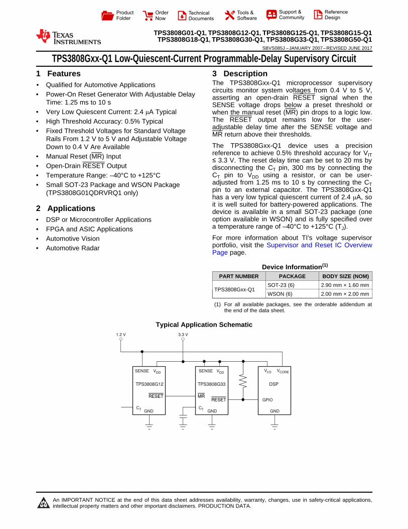
1.2 V 3.3 V TPS3808G12 TPS3808G33 DSP SENSE V DD V DD SENSE V I/O V CORE GPIO GND GND GND RESET MR C T C T RESET Product Folder Order Now Technical Documents Tools & Software Support & Community Reference Design An IMPORTANT NOTICE at the end of this data sheet addresses availability, warranty, changes, use in safety-critical applications, intellectual property matters and other important disclaimers. PRODUCTION DATA. TPS3808G01-Q1, TPS3808G12-Q1, TPS3808G125-Q1, TPS3808G15-Q1 TPS3808G18-Q1, TPS3808G30-Q1, TPS3808G33-Q1, TPS3808G50-Q1 SBVS085J – JANUARY 2007 – REVISED JUNE 2017 TPS3808Gxx-Q1 Low-Quiescent-Current Programmable-Delay Supervisory Circuit 1 1 Features 1• Qualified for Automotive Applications • Power-On Reset Generator With Adjustable Delay Time: 1.25 ms to 10 s • Very Low Quiescent Current: 2.4 μA Typical • High Threshold Accuracy: 0.5% Typical • Fixed Threshold Voltages for Standard Voltage Rails From 1.2 V to 5 V and Adjustable Voltage Down to 0.4 V Are Available • Manual Reset (MR) Input • Open-Drain RESET Output • Temperature Range: –40°C to +125°C • Small SOT-23 Package and WSON Package (TPS3808G01QDRVRQ1 only) 2 Applications • DSP or Microcontroller Applications • FPGA and ASIC Applications • Automotive Vision • Automotive Radar 3 Description The TPS3808Gxx-Q1 microprocessor supervisory circuits monitor system voltages from 0.4 V to 5 V, asserting an open-drain RESET signal when the SENSE voltage drops below a preset threshold or when the manual reset (MR) pin drops to a logic low. The RESET output remains low for the user- adjustable delay time after the SENSE voltage and MR return above their thresholds. The TPS3808Gxx-Q1 device uses a precision reference to achieve 0.5% threshold accuracy for V IT ≤ 3.3 V. The reset delay time can be set to 20 ms by disconnecting the C T pin, 300 ms by connecting the C T pin to V DD using a resistor, or can be user- adjusted from 1.25 ms to 10 s by connecting the C T pin to an external capacitor. The TPS3808Gxx-Q1 has a very low typical quiescent current of 2.4 μA, so it is well suited for battery-powered applications. The device is available in a small SOT-23 package (one option available in WSON) and is fully specified over a temperature range of –40°C to +125°C (T J ). For more information about TI's voltage supervisor portfolio, visit the Supervisor and Reset IC Overview Page page. Device Information (1) PART NUMBER PACKAGE BODY SIZE (NOM) TPS3808Gxx-Q1 SOT-23 (6) 2.90 mm × 1.60 mm WSON (6) 2.00 mm × 2.00 mm (1) For all available packages, see the orderable addendum at the end of the data sheet. Typical Application Schematic
Transcript of TPS3808Gxx-Q1 Low-Quiescent-Current Programmable · PDF fileportfolio, visit the Supervisor...
1.2 V 3.3 V
TPS3808G12 TPS3808G33 DSP
SENSE VDDVDD SENSE VI/O VCORE
GPIO
GNDGNDGND
RESET MR
CTCT
RESET
Product
Folder
Order
Now
Technical
Documents
Tools &
Software
Support &Community
ReferenceDesign
An IMPORTANT NOTICE at the end of this data sheet addresses availability, warranty, changes, use in safety-critical applications,intellectual property matters and other important disclaimers. PRODUCTION DATA.
TPS3808G01-Q1, TPS3808G12-Q1, TPS3808G125-Q1, TPS3808G15-Q1TPS3808G18-Q1, TPS3808G30-Q1, TPS3808G33-Q1, TPS3808G50-Q1
SBVS085J –JANUARY 2007–REVISED JUNE 2017
TPS3808Gxx-Q1 Low-Quiescent-Current Programmable-Delay Supervisory Circuit
1
1 Features1• Qualified for Automotive Applications• Power-On Reset Generator With Adjustable Delay
Time: 1.25 ms to 10 s• Very Low Quiescent Current: 2.4 μA Typical• High Threshold Accuracy: 0.5% Typical• Fixed Threshold Voltages for Standard Voltage
Rails From 1.2 V to 5 V and Adjustable VoltageDown to 0.4 V Are Available
• Manual Reset (MR) Input• Open-Drain RESET Output• Temperature Range: –40°C to +125°C• Small SOT-23 Package and WSON Package
(TPS3808G01QDRVRQ1 only)
2 Applications• DSP or Microcontroller Applications• FPGA and ASIC Applications• Automotive Vision• Automotive Radar
3 DescriptionThe TPS3808Gxx-Q1 microprocessor supervisorycircuits monitor system voltages from 0.4 V to 5 V,asserting an open-drain RESET signal when theSENSE voltage drops below a preset threshold orwhen the manual reset (MR) pin drops to a logic low.The RESET output remains low for the user-adjustable delay time after the SENSE voltage andMR return above their thresholds.
The TPS3808Gxx-Q1 device uses a precisionreference to achieve 0.5% threshold accuracy for VIT≤ 3.3 V. The reset delay time can be set to 20 ms bydisconnecting the CT pin, 300 ms by connecting theCT pin to VDD using a resistor, or can be user-adjusted from 1.25 ms to 10 s by connecting the CTpin to an external capacitor. The TPS3808Gxx-Q1has a very low typical quiescent current of 2.4 μA, soit is well suited for battery-powered applications. Thedevice is available in a small SOT-23 package (oneoption available in WSON) and is fully specified overa temperature range of –40°C to +125°C (TJ).
For more information about TI's voltage supervisorportfolio, visit the Supervisor and Reset IC OverviewPage page.
Device Information(1)
PART NUMBER PACKAGE BODY SIZE (NOM)
TPS3808Gxx-Q1SOT-23 (6) 2.90 mm × 1.60 mmWSON (6) 2.00 mm × 2.00 mm
(1) For all available packages, see the orderable addendum atthe end of the data sheet.
Typical Application Schematic
2
TPS3808G01-Q1, TPS3808G12-Q1, TPS3808G125-Q1, TPS3808G15-Q1TPS3808G18-Q1, TPS3808G30-Q1, TPS3808G33-Q1, TPS3808G50-Q1SBVS085J –JANUARY 2007–REVISED JUNE 2017 www.ti.com
Product Folder Links: TPS3808G01-Q1 TPS3808G12-Q1 TPS3808G125-Q1 TPS3808G15-Q1 TPS3808G18-Q1TPS3808G30-Q1 TPS3808G33-Q1 TPS3808G50-Q1
Submit Documentation Feedback Copyright © 2007–2017, Texas Instruments Incorporated
Table of Contents1 Features .................................................................. 12 Applications ........................................................... 13 Description ............................................................. 14 Revision History..................................................... 25 Device Comparison Table ..................................... 36 Pin Configuration and Functions ......................... 37 Specifications......................................................... 4
7.1 Absolute Maximum Ratings ...................................... 47.2 ESD Ratings.............................................................. 47.3 Recommended Operating Conditions....................... 47.4 Thermal Information .................................................. 57.5 Electrical Characteristics........................................... 57.6 Timing Requirements ................................................ 67.7 Typical Characteristics .............................................. 7
8 Detailed Description .............................................. 88.1 Overview ................................................................... 88.2 Functional Block Diagrams ....................................... 8
8.3 Feature Description................................................... 98.4 Device Functional Modes........................................ 11
9 Applications and Implementation ...................... 129.1 Application Information............................................ 129.2 Typical Application .................................................. 12
10 Power Supply Recommendations ..................... 1411 Layout................................................................... 14
11.1 Layout Guidelines ................................................. 1411.2 Layout Example .................................................... 14
12 Device and Documentation Support ................. 1512.1 Related Links ........................................................ 1512.2 Receiving Notification of Documentation Updates 1512.3 Community Resources.......................................... 1512.4 Trademarks ........................................................... 1512.5 Electrostatic Discharge Caution............................ 1512.6 Glossary ................................................................ 15
13 Mechanical, Packaging, and OrderableInformation ........................................................... 15
4 Revision HistoryNOTE: Page numbers for previous revisions may differ from page numbers in the current version.
Changes from Revision I (June 2015) to Revision J Page
• Added column for WSON pins .............................................................................................................................................. 3• Changed unit for last row of td row in Timing Requirements from "ms" to "s" and "TYP" to "NOM" in middle unit column... 6
Changes from Revision H (June 2012) to Revision I Page
• Added ESD Ratings table, Feature Description section, Device Functional Modes, Application and Implementationsection, Power Supply Recommendations section, Layout section, Device and Documentation Support section, andMechanical, Packaging, and Orderable Information section ................................................................................................. 1
Changes from Revision G (November, 2010) to Revision H Page
• Changed ISENSE from µA to nA................................................................................................................................................ 5
RESET
GND
MR
1
2
3
6
5
4 CT
SENSE
VDD
RESET
GND
MR
6
5
4
VDD
SENSE
CT
1
2
3
3
TPS3808G01-Q1, TPS3808G12-Q1, TPS3808G125-Q1, TPS3808G15-Q1TPS3808G18-Q1, TPS3808G30-Q1, TPS3808G33-Q1, TPS3808G50-Q1
www.ti.com SBVS085J –JANUARY 2007–REVISED JUNE 2017
Product Folder Links: TPS3808G01-Q1 TPS3808G12-Q1 TPS3808G125-Q1 TPS3808G15-Q1 TPS3808G18-Q1TPS3808G30-Q1 TPS3808G33-Q1 TPS3808G50-Q1
Submit Documentation FeedbackCopyright © 2007–2017, Texas Instruments Incorporated
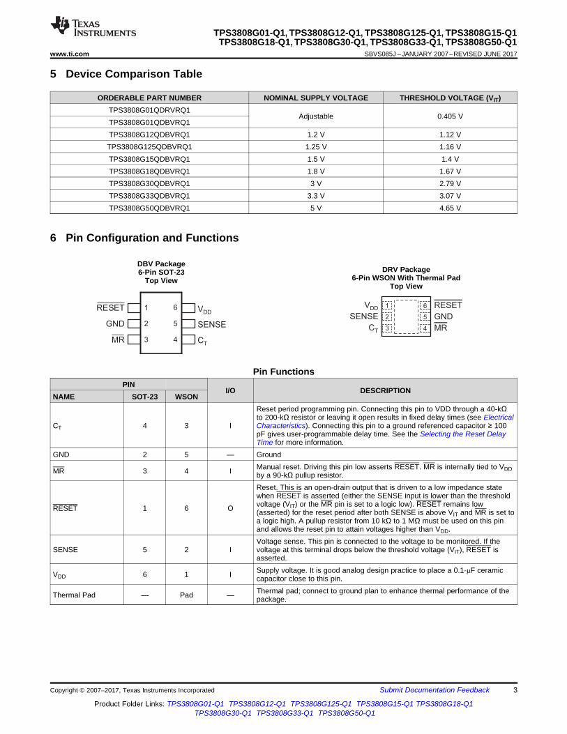
5 Device Comparison Table
ORDERABLE PART NUMBER NOMINAL SUPPLY VOLTAGE THRESHOLD VOLTAGE (VIT)TPS3808G01QDRVRQ1
Adjustable 0.405 VTPS3808G01QDBVRQ1TPS3808G12QDBVRQ1 1.2 V 1.12 VTPS3808G125QDBVRQ1 1.25 V 1.16 VTPS3808G15QDBVRQ1 1.5 V 1.4 VTPS3808G18QDBVRQ1 1.8 V 1.67 VTPS3808G30QDBVRQ1 3 V 2.79 VTPS3808G33QDBVRQ1 3.3 V 3.07 VTPS3808G50QDBVRQ1 5 V 4.65 V
6 Pin Configuration and Functions
DBV Package6-Pin SOT-23
Top ViewDRV Package
6-Pin WSON With Thermal PadTop View
Pin FunctionsPIN
I/O DESCRIPTIONNAME SOT-23 WSON
CT 4 3 I
Reset period programming pin. Connecting this pin to VDD through a 40-kΩto 200-kΩ resistor or leaving it open results in fixed delay times (see ElectricalCharacteristics). Connecting this pin to a ground referenced capacitor ≥ 100pF gives user-programmable delay time. See the Selecting the Reset DelayTime for more information.
GND 2 5 — Ground
MR 3 4 I Manual reset. Driving this pin low asserts RESET. MR is internally tied to VDDby a 90-kΩ pullup resistor.
RESET 1 6 O
Reset. This is an open-drain output that is driven to a low impedance statewhen RESET is asserted (either the SENSE input is lower than the thresholdvoltage (VIT) or the MR pin is set to a logic low). RESET remains low(asserted) for the reset period after both SENSE is above VIT and MR is set toa logic high. A pullup resistor from 10 kΩ to 1 MΩ must be used on this pinand allows the reset pin to attain voltages higher than VDD.
SENSE 5 2 IVoltage sense. This pin is connected to the voltage to be monitored. If thevoltage at this terminal drops below the threshold voltage (VIT), RESET isasserted.
VDD 6 1 I Supply voltage. It is good analog design practice to place a 0.1-μF ceramiccapacitor close to this pin.
Thermal Pad — Pad — Thermal pad; connect to ground plan to enhance thermal performance of thepackage.
4
TPS3808G01-Q1, TPS3808G12-Q1, TPS3808G125-Q1, TPS3808G15-Q1TPS3808G18-Q1, TPS3808G30-Q1, TPS3808G33-Q1, TPS3808G50-Q1SBVS085J –JANUARY 2007–REVISED JUNE 2017 www.ti.com
Product Folder Links: TPS3808G01-Q1 TPS3808G12-Q1 TPS3808G125-Q1 TPS3808G15-Q1 TPS3808G18-Q1TPS3808G30-Q1 TPS3808G33-Q1 TPS3808G50-Q1
Submit Documentation Feedback Copyright © 2007–2017, Texas Instruments Incorporated
(1) Stresses beyond those listed under Absolute Maximum Ratings may cause permanent damage to the device. These are stress ratingsonly, and functional operation of the device at these or any other conditions beyond those indicated under the Electric Characteristics isnot implied. Exposure to absolute-maximum-rated conditions for extended periods may affect device reliability.
(2) Due to the low dissipated power in this device, it is assumed that TJ = TA.
7 Specifications
7.1 Absolute Maximum Ratingsover operating junction temperature range (unless otherwise noted) (1)
MIN MAX UNITVDD Input voltage –0.3 7 VVCT CT voltage –0.3 (VDD + 0.3) VVMR,VRESET,VSENSE
MR, RESET, SENSE voltage –0.3 7 V
IRESET RESET pin current 5 mATJ Operating junction temperature (2) –40 150 °CTstg Storage temperature –65 150 °C
(1) AEC Q100-002 indicates HBM stressing is done in accordance with the ANSI/ESDA/JEDEC JS-001 specification.
7.2 ESD RatingsVALUE UNIT
TPS3808G125QDBVRQ1 IN SOT-23 PACKAGE
V(ESD)Electrostaticdischarge
Human body model (HBM), per AEC Q100-002 (1) ±2000VCharged device model (CDM), per AEC Q100-011 ±1000
Machine Model (MM) ±50TPS3808GXX-Q1 IN SOT-23 PACKAGE
V(ESD)Electrostaticdischarge
Human body model (HBM), per AEC Q100-002 (1) ±2000V
Charged device model (CDM), per AEC Q100-011 ±500TPS3808G01QDRVRQ1 IN SON PACKAGE
V(ESD)Electrostaticdischarge
Human body model (HBM), per AEC Q100-002 (1) ±2000VCharged device model (CDM), per AEC Q100-011 ±500
Machine Model (MM) ±50
7.3 Recommended Operating Conditionsover operating free-air temperature range (unless otherwise noted)
MIN NOM MAX UNITVDD input supply 1.8 6.5 VVSENSE SENSE pin voltage 0 VDD VMR Manual reset pin voltage 0 VDD V
5
TPS3808G01-Q1, TPS3808G12-Q1, TPS3808G125-Q1, TPS3808G15-Q1TPS3808G18-Q1, TPS3808G30-Q1, TPS3808G33-Q1, TPS3808G50-Q1
www.ti.com SBVS085J –JANUARY 2007–REVISED JUNE 2017
Product Folder Links: TPS3808G01-Q1 TPS3808G12-Q1 TPS3808G125-Q1 TPS3808G15-Q1 TPS3808G18-Q1TPS3808G30-Q1 TPS3808G33-Q1 TPS3808G50-Q1
Submit Documentation FeedbackCopyright © 2007–2017, Texas Instruments Incorporated
(1) For more information about traditional and new thermal metrics, see the Semiconductor and IC Package Thermal Metrics applicationreport.
7.4 Thermal Information
THERMAL METRIC (1)TPS3808Gxx-Q1
UNITDBV (SOT-23) DRV (WSON)6 PINS 6 PINS
RθJA Junction-to-ambient thermal resistance 180.9 178.1 °C/WRθJC(top) Junction-to-case (top) thermal resistance 117.8 95.6 °C/WRθJB Junction-to-board thermal resistance 27.8 135 °C/WψJT Junction-to-top characterization parameter 18.9 6.3 °C/WψJB Junction-to-board characterization parameter 27.3 136.6 °C/WRθJC(bot) Junction-to-case (bottom) thermal resistance N/A 7.3 °C/W
(1) Power-up reset voltage is the lowest supply voltage (VDD) at which RESET becomes active (trise(VDD) ≥ 15 μs/V).
7.5 Electrical Characteristics1.8 V ≤ VDD ≤ 6.5 V, RLRESET = 100 kΩ, CLRESET = 50 pF, over operating temperature range (TJ = –40°C to +125°C) (unlessotherwise noted), typical values at TJ = 25°C
PARAMETER TEST CONDITIONS MIN TYP MAX UNITVDD Input supply range 1.8 6.5 V
IDD Supply current (into VDD pin)
VDD = 3.3 V, RESET not asserted,MR, RESET, CT open 2.4 5
μAVDD = 6.5 V, RESET not asserted,MR, RESET, CT open 2.7 6
VOL Low-level output voltage1.3 V ≤ VDD < 1.8 V, IOL = 0.4 mA 0.3
V1.8 V ≤ VDD ≤ 6.5 V, IOL = 1 mA 0.4
Power-up reset voltage (1) VOL (max) = 0.2 V, I RESET = 15 μA 0.8 V
VITNegative-going inputthreshold accuracy
TPS3808G01-Q1 –2% ±1% 2%VIT ≤ 3.3 V –1.5% ±0.5% 1.5%3.3 V < VIT ≤ 5 V –2% ±1% 2%VIT ≤ 3.3 V
–40°C < TJ < 85°C–1.25% ±0.5% 1.25%
3.3 V < VIT ≤ 5 V –1.5% ±0.5% 1.5%
VHYS Hysteresis on VIT pinTPS3808G01-Q1 1.5 3
%VIT–40°C < TJ < 85°C 1 21 2.5
R MR MR internal pullup resistance VSENSE = VIT 70 90 kΩ
ISENSE Input current at SENSE pinTPS3808G01-Q1 –25 25 nAVSENSE = 6.5 V 1.7 μA
IOH RESET leakage current V RESET = 6.5 V, RESET not asserted 300 nA
CIN Input capacitance, any pinCT pin VIN = 0 V to VDD 5
pFOther pins VIN = 0 V to 6.5 V 5
VIL MR logic low input 0 0.3 VDD VVIH MR logic high input 0.7 VDD VDD V
Time
0.8V
0.0V
VIT + VHYS
VIT
0.7VDD
0.3VDD
MR
SENSE
RESET
VDD
tD tD tD
tD = Reset Delay
= Undefined State
6
TPS3808G01-Q1, TPS3808G12-Q1, TPS3808G125-Q1, TPS3808G15-Q1TPS3808G18-Q1, TPS3808G30-Q1, TPS3808G33-Q1, TPS3808G50-Q1SBVS085J –JANUARY 2007–REVISED JUNE 2017 www.ti.com
Product Folder Links: TPS3808G01-Q1 TPS3808G12-Q1 TPS3808G125-Q1 TPS3808G15-Q1 TPS3808G18-Q1TPS3808G30-Q1 TPS3808G33-Q1 TPS3808G50-Q1
Submit Documentation Feedback Copyright © 2007–2017, Texas Instruments Incorporated
7.6 Timing RequirementsMIN NOM MAX UNIT
tdRESET delaytime
CT = Open
See Figure 1
12 20 28msCT = VDD 180 300 420
CT = 100 pF 0.75 1.25 1.75CT = 180 nF 0.7 1.2 1.7 s
tpHL
Propagationdelay MR to RESET VIH = 0.7 VDD, VIL = 0.3 VDD 150 ns
High-level tolow-levelRESET delay
SENSE toRESET VIH = 1.05 VIT, VIL = 0.95 VIT 20 μs
twMaximumtransientduration
SENSE VIH = 1.05 VIT, VIL = 0.95 VIT 20μs
MR VIH = 0.7 VDD, VIL = 0.3 VDD 0.001
Figure 1. MR and SENSE Reset Timing Diagram

4.5
4.0
3.5
3.0
2.5
2.0
1.5
1.0
0.5
0
0 0.5 1.0 1.5 2.0 2.5 3.0 3.5 4.0
VO
LLow
−L
evelR
ES
ET
Voltage
(V)
VDD = 1.8V
RESET Current (mA)
0 0.5 1.0 1.5 2.0 2.5 3.0 3.5 4.0 4.5 5.0
0.8
0.7
0.6
0.5
0.4
0.3
0.2
0.1
0
VO
LLo
w−
Leve
lR
ES
ET
Vo
ltag
e(V
)
RESET Current (mA)
VDD = 3.3V
VDD = 6.5 V
10
8
6
4
2
0
10 30 50 70 90 110 130
Temperature (°C)
−50 −30 −10
−10
−8
−6
−4
−2
Norm
aliz
ed
RE
SE
TT
imeout
Period
(%
)
1.0
0.8
0.6
0.4
0.2
0
10 30 50 70 90 110 130
Temperature (°C)
−50 −30 −10
−1.0
−0.8
−0.6
−0.4
−0.2
Norm
aliz
ed V
IT(%
)
7
TPS3808G01-Q1, TPS3808G12-Q1, TPS3808G125-Q1, TPS3808G15-Q1TPS3808G18-Q1, TPS3808G30-Q1, TPS3808G33-Q1, TPS3808G50-Q1
www.ti.com SBVS085J –JANUARY 2007–REVISED JUNE 2017
Product Folder Links: TPS3808G01-Q1 TPS3808G12-Q1 TPS3808G125-Q1 TPS3808G15-Q1 TPS3808G18-Q1TPS3808G30-Q1 TPS3808G33-Q1 TPS3808G50-Q1
Submit Documentation FeedbackCopyright © 2007–2017, Texas Instruments Incorporated
7.7 Typical CharacteristicsAt TJ = 25°C, VDD = 3.3 V, RLRESET = 100 kΩ, and CLRESET = 50 pF (unless otherwise noted)
Figure 2. Normalized RESET Time-out Period vsTemperature (CT = Open, CT = VDD, CT = Any)
Figure 3. Normalized Sense Threshold Voltage (VIT) vsTemperature
Figure 4. Low-Level RESET Voltage vs RESET Current Figure 5. Low-Level RESET Voltage vs RESET Current
Reset
LogicTimer
+
−
90k
VDD
VDD
GND
0.4 VVREF
SENSE
MR
CT
RESET
R1
R2
R1 + R2 = 4 MW
Reset
LogicTimer
+
−
90k
VDD
VDD
GND
0.4 VVREF
SENSE
MR
CT
RESET
8
TPS3808G01-Q1, TPS3808G12-Q1, TPS3808G125-Q1, TPS3808G15-Q1TPS3808G18-Q1, TPS3808G30-Q1, TPS3808G33-Q1, TPS3808G50-Q1SBVS085J –JANUARY 2007–REVISED JUNE 2017 www.ti.com
Product Folder Links: TPS3808G01-Q1 TPS3808G12-Q1 TPS3808G125-Q1 TPS3808G15-Q1 TPS3808G18-Q1TPS3808G30-Q1 TPS3808G33-Q1 TPS3808G50-Q1
Submit Documentation Feedback Copyright © 2007–2017, Texas Instruments Incorporated
8 Detailed Description
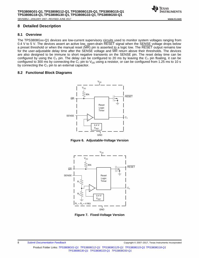
8.1 OverviewThe TPS3808Gxx-Q1 devices are low-current supervisory circuits used to monitor system voltages ranging from0.4 V to 5 V. The devices assert an active low, open-drain RESET signal when the SENSE voltage drops belowa preset threshold or when the manual reset (MR) pin is asserted to a logic low. The RESET output remains lowfor the user-adjustable delay time after the SENSE voltage and MR return above their thresholds. The devicesare also designed to be immune to short negative transients on the SENSE pin. The reset delay time can beconfigured by using the CT pin. The delay can be configured to 20 ms by leaving the CT pin floating, it can beconfigured to 300 ms by connecting the CT pin to VDD using a resistor, or can be configured from 1.25 ms to 10 sby connecting the CT pin to an external capacitor.
8.2 Functional Block Diagrams
Figure 6. Adjustable-Voltage Version
Figure 7. Fixed-Voltage Version
100
10
1
0 5 10 15 20 30 35 4525
Overdrive (%VIT)
5040
Tra
nsie
nt D
ura
tion
belo
w V
IT(m
s)
RESET OCCURS
ABOVE THE CURVE
VDD
VIT
Overdrive
Voltage
Transient
Duration
9
TPS3808G01-Q1, TPS3808G12-Q1, TPS3808G125-Q1, TPS3808G15-Q1TPS3808G18-Q1, TPS3808G30-Q1, TPS3808G33-Q1, TPS3808G50-Q1
www.ti.com SBVS085J –JANUARY 2007–REVISED JUNE 2017
Product Folder Links: TPS3808G01-Q1 TPS3808G12-Q1 TPS3808G125-Q1 TPS3808G15-Q1 TPS3808G18-Q1TPS3808G30-Q1 TPS3808G33-Q1 TPS3808G50-Q1
Submit Documentation FeedbackCopyright © 2007–2017, Texas Instruments Incorporated
8.3 Feature Description
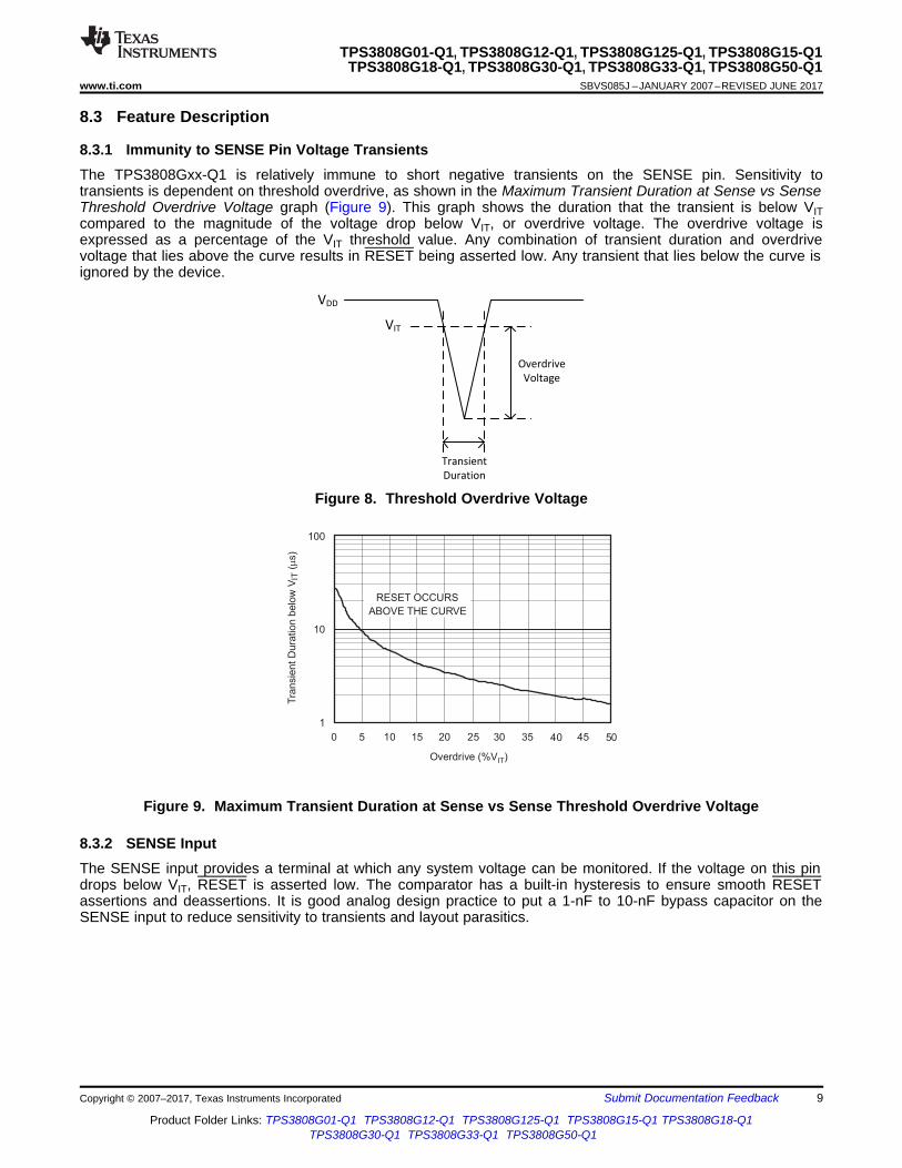
8.3.1 Immunity to SENSE Pin Voltage TransientsThe TPS3808Gxx-Q1 is relatively immune to short negative transients on the SENSE pin. Sensitivity totransients is dependent on threshold overdrive, as shown in the Maximum Transient Duration at Sense vs SenseThreshold Overdrive Voltage graph (Figure 9). This graph shows the duration that the transient is below VITcompared to the magnitude of the voltage drop below VIT, or overdrive voltage. The overdrive voltage isexpressed as a percentage of the VIT threshold value. Any combination of transient duration and overdrivevoltage that lies above the curve results in RESET being asserted low. Any transient that lies below the curve isignored by the device.
Figure 8. Threshold Overdrive Voltage
Figure 9. Maximum Transient Duration at Sense vs Sense Threshold Overdrive Voltage
8.3.2 SENSE InputThe SENSE input provides a terminal at which any system voltage can be monitored. If the voltage on this pindrops below VIT, RESET is asserted low. The comparator has a built-in hysteresis to ensure smooth RESETassertions and deassertions. It is good analog design practice to put a 1-nF to 10-nF bypass capacitor on theSENSE input to reduce sensitivity to transients and layout parasitics.

3.3V
TPS3808xxx
VDD
SENSE
CT
90kW
G ND
1.2V 3.3V
TPS3808G12 TPS3808G33 DSP
SENSE VDD
VDD
SENSE VI/O
VCORE
GPIO
GNDGNDGND
RESET MR
CT
CT
RESET
VIN
TPS3808G01
VDD
SENSE
GND
RESET
R1
R21nF
VIT′= (1 + )0.405R1
R2
VOUT
10
TPS3808G01-Q1, TPS3808G12-Q1, TPS3808G125-Q1, TPS3808G15-Q1TPS3808G18-Q1, TPS3808G30-Q1, TPS3808G33-Q1, TPS3808G50-Q1SBVS085J –JANUARY 2007–REVISED JUNE 2017 www.ti.com
Product Folder Links: TPS3808G01-Q1 TPS3808G12-Q1 TPS3808G125-Q1 TPS3808G15-Q1 TPS3808G18-Q1TPS3808G30-Q1 TPS3808G33-Q1 TPS3808G50-Q1
Submit Documentation Feedback Copyright © 2007–2017, Texas Instruments Incorporated
Feature Description (continued)The TPS3808G01-Q1 can be used to monitor any voltage rail down to 0.405 V using the circuit shown inFigure 10.
Figure 10. Using the TPS3808G01-Q1 to Monitor a User-Defined Threshold Voltage
8.3.3 Manual Reset (MR) InputThe manual reset (MR) input allows a processor or other logic circuits to initiate a reset. A logic low (0.3 VDD) onMR causes RESET to assert low. After MR returns to a logic high and SENSE is above its reset threshold,RESET is deasserted high after the user-defined reset delay expires. MR is internally tied to VDD using a 90-kΩresistor, so this pin can be left unconnected if MR is not used.
See Figure 11 for how MR can be used to monitor multiple system voltages. If the logic signal driving MR doesnot go fully to VDD, there will be some additional current draw into VDD as a result of the internal pullup resistor onMR. To minimize current draw, a logic-level FET can be used as shown in Figure 12.
Figure 11. Using MR to Monitor Multiple System Voltages
Figure 12. Using an External MOSFET to Minimize IDD When MR Signal Does Not Go to VDD
3T DC (nF) t (s) 0.5 10 (s) 175-é ù= - ´ ´
ë û
Delay (s) = CT (nF) + 0.5 x 10⁻³ (s)20ms Delay300ms Delay
(c)(b)(a)175
3.3V
TPS3808G33
VDD
SENSE
CT RESET
3.3V
TPS3808G33
VDD
SENSE
CT
CT
RESET
3.3V
TPS3808G33
VDDSENSE
CT
50kW
RESET
11
TPS3808G01-Q1, TPS3808G12-Q1, TPS3808G125-Q1, TPS3808G15-Q1TPS3808G18-Q1, TPS3808G30-Q1, TPS3808G33-Q1, TPS3808G50-Q1
www.ti.com SBVS085J –JANUARY 2007–REVISED JUNE 2017
Product Folder Links: TPS3808G01-Q1 TPS3808G12-Q1 TPS3808G125-Q1 TPS3808G15-Q1 TPS3808G18-Q1TPS3808G30-Q1 TPS3808G33-Q1 TPS3808G50-Q1
Submit Documentation FeedbackCopyright © 2007–2017, Texas Instruments Incorporated
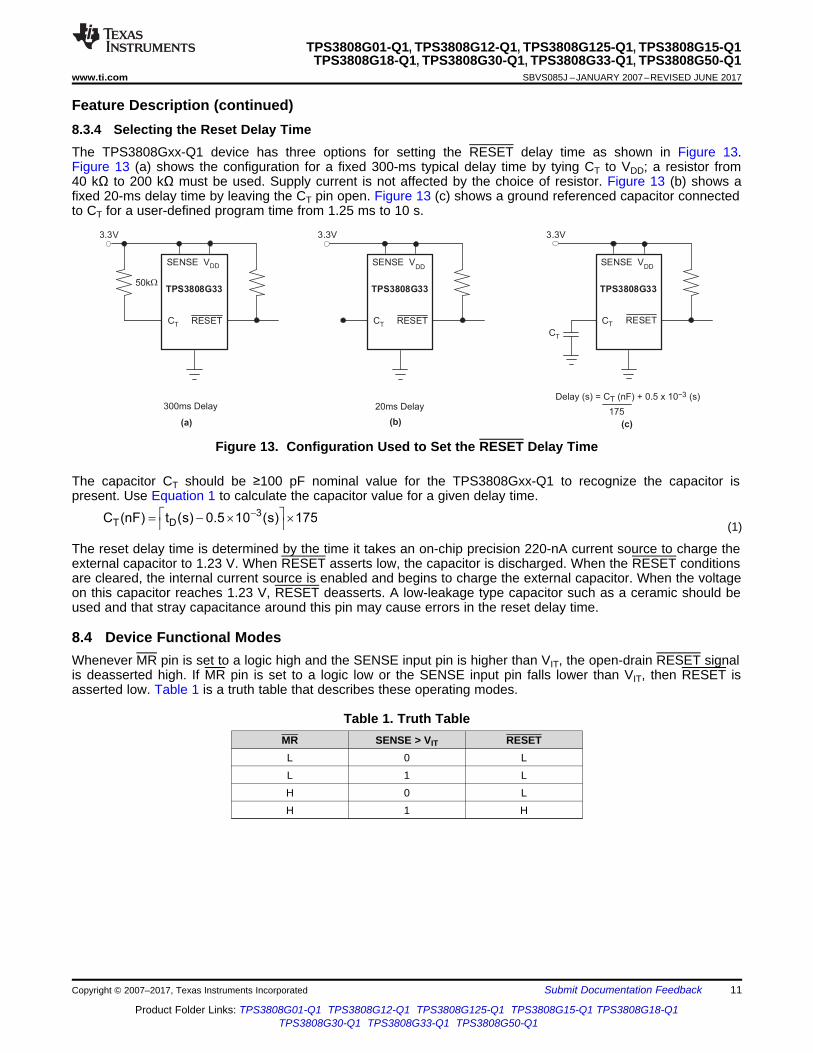
Feature Description (continued)8.3.4 Selecting the Reset Delay TimeThe TPS3808Gxx-Q1 device has three options for setting the RESET delay time as shown in Figure 13.Figure 13 (a) shows the configuration for a fixed 300-ms typical delay time by tying CT to VDD; a resistor from40 kΩ to 200 kΩ must be used. Supply current is not affected by the choice of resistor. Figure 13 (b) shows afixed 20-ms delay time by leaving the CT pin open. Figure 13 (c) shows a ground referenced capacitor connectedto CT for a user-defined program time from 1.25 ms to 10 s.
Figure 13. Configuration Used to Set the RESET Delay Time
The capacitor CT should be ≥100 pF nominal value for the TPS3808Gxx-Q1 to recognize the capacitor ispresent. Use Equation 1 to calculate the capacitor value for a given delay time.
(1)
The reset delay time is determined by the time it takes an on-chip precision 220-nA current source to charge theexternal capacitor to 1.23 V. When RESET asserts low, the capacitor is discharged. When the RESET conditionsare cleared, the internal current source is enabled and begins to charge the external capacitor. When the voltageon this capacitor reaches 1.23 V, RESET deasserts. A low-leakage type capacitor such as a ceramic should beused and that stray capacitance around this pin may cause errors in the reset delay time.
8.4 Device Functional ModesWhenever MR pin is set to a logic high and the SENSE input pin is higher than VIT, the open-drain RESET signalis deasserted high. If MR pin is set to a logic low or the SENSE input pin falls lower than VIT, then RESET isasserted low. Table 1 is a truth table that describes these operating modes.
Table 1. Truth TableMR SENSE > VIT RESETL 0 LL 1 LH 0 LH 1 H
VDD
TPS3808G01-Q1
SENSE
CT
___
MR
_____
RESET
GND
Processor
VDD
RESET
3.3V
50 lQ
GNDCT
R1
R21 nF
VDD
TPS3808G33-Q1
SENSE
CT
___
MR
_____
RESET
GND
Processor
VDD
RESET
3.3V
50 lQ
GNDCT
12
TPS3808G01-Q1, TPS3808G12-Q1, TPS3808G125-Q1, TPS3808G15-Q1TPS3808G18-Q1, TPS3808G30-Q1, TPS3808G33-Q1, TPS3808G50-Q1SBVS085J –JANUARY 2007–REVISED JUNE 2017 www.ti.com
Product Folder Links: TPS3808G01-Q1 TPS3808G12-Q1 TPS3808G125-Q1 TPS3808G15-Q1 TPS3808G18-Q1TPS3808G30-Q1 TPS3808G33-Q1 TPS3808G50-Q1
Submit Documentation Feedback Copyright © 2007–2017, Texas Instruments Incorporated
9 Applications and Implementation
NOTEInformation in the following applications sections is not part of the TI componentspecification, and TI does not warrant its accuracy or completeness. TI’s customers areresponsible for determining suitability of components for their purposes. Customers shouldvalidate and test their design implementation to confirm system functionality.
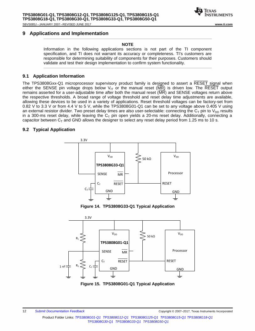
9.1 Application InformationThe TPS3808Gxx-Q1 microprocessor supervisory product family is designed to assert a RESET signal wheneither the SENSE pin voltage drops below VIT or the manual reset (MR) is driven low. The RESET outputremains asserted for a user-adjustable time after both the manual reset (MR) and SENSE voltages return abovethe respective thresholds. A broad range of voltage threshold and reset delay time adjustments are available,allowing these devices to be used in a variety of applications. Reset threshold voltages can be factory-set from0.82 V to 3.3 V or from 4.4 V to 5 V, while the TPS3808G01-Q1 can be set to any voltage above 0.405 V usingan external resistor divider. Two preset delay times are also user-selectable: connecting the CT pin to VDD resultsin a 300-ms reset delay, while leaving the CT pin open yields a 20-ms reset delay. Additionally, connecting acapacitor between CT and GND allows the designer to select any reset delay period from 1.25 ms to 10 s.
9.2 Typical Application
Figure 14. TPS3808G33-Q1 Typical Application
Figure 15. TPS3808G01-Q1 Typical Application
0 1 2 3 4 5 6 7
4.0
3.5
3.0
2.5
2.0
1.5
1.0
0.5
0
−40ºC
25ºC
85ºC
125ºC
I DD
(A
)m
VDD (V)
100
10
1
0.1
0.01
0.0010.0001 0.001 0.01 0.1
CT (mF)
101
−40°C, 25°C, 125°C
RE
SE
TT
imeout
(sec)
13
TPS3808G01-Q1, TPS3808G12-Q1, TPS3808G125-Q1, TPS3808G15-Q1TPS3808G18-Q1, TPS3808G30-Q1, TPS3808G33-Q1, TPS3808G50-Q1
www.ti.com SBVS085J –JANUARY 2007–REVISED JUNE 2017
Product Folder Links: TPS3808G01-Q1 TPS3808G12-Q1 TPS3808G125-Q1 TPS3808G15-Q1 TPS3808G18-Q1TPS3808G30-Q1 TPS3808G33-Q1 TPS3808G50-Q1
Submit Documentation FeedbackCopyright © 2007–2017, Texas Instruments Incorporated
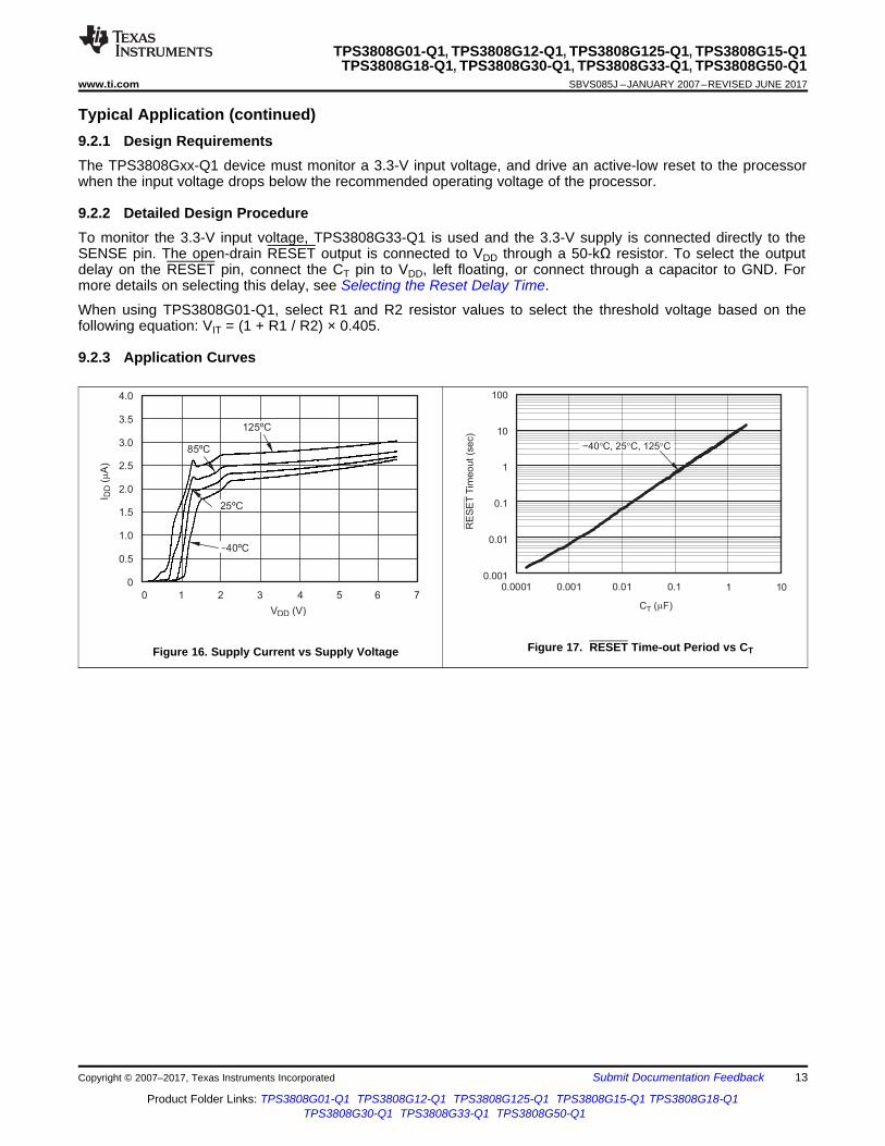
Typical Application (continued)9.2.1 Design RequirementsThe TPS3808Gxx-Q1 device must monitor a 3.3-V input voltage, and drive an active-low reset to the processorwhen the input voltage drops below the recommended operating voltage of the processor.
9.2.2 Detailed Design ProcedureTo monitor the 3.3-V input voltage, TPS3808G33-Q1 is used and the 3.3-V supply is connected directly to theSENSE pin. The open-drain RESET output is connected to VDD through a 50-kΩ resistor. To select the outputdelay on the RESET pin, connect the CT pin to VDD, left floating, or connect through a capacitor to GND. Formore details on selecting this delay, see Selecting the Reset Delay Time.
When using TPS3808G01-Q1, select R1 and R2 resistor values to select the threshold voltage based on thefollowing equation: VIT = (1 + R1 / R2) × 0.405.
9.2.3 Application Curves
Figure 16. Supply Current vs Supply Voltage Figure 17. RESET Time-out Period vs CT
2
3
5
4
CT
CVDDReset Output
Manual Reset
Signal
Input Supply
1 6
14
TPS3808G01-Q1, TPS3808G12-Q1, TPS3808G125-Q1, TPS3808G15-Q1TPS3808G18-Q1, TPS3808G30-Q1, TPS3808G33-Q1, TPS3808G50-Q1SBVS085J –JANUARY 2007–REVISED JUNE 2017 www.ti.com
Product Folder Links: TPS3808G01-Q1 TPS3808G12-Q1 TPS3808G125-Q1 TPS3808G15-Q1 TPS3808G18-Q1TPS3808G30-Q1 TPS3808G33-Q1 TPS3808G50-Q1
Submit Documentation Feedback Copyright © 2007–2017, Texas Instruments Incorporated
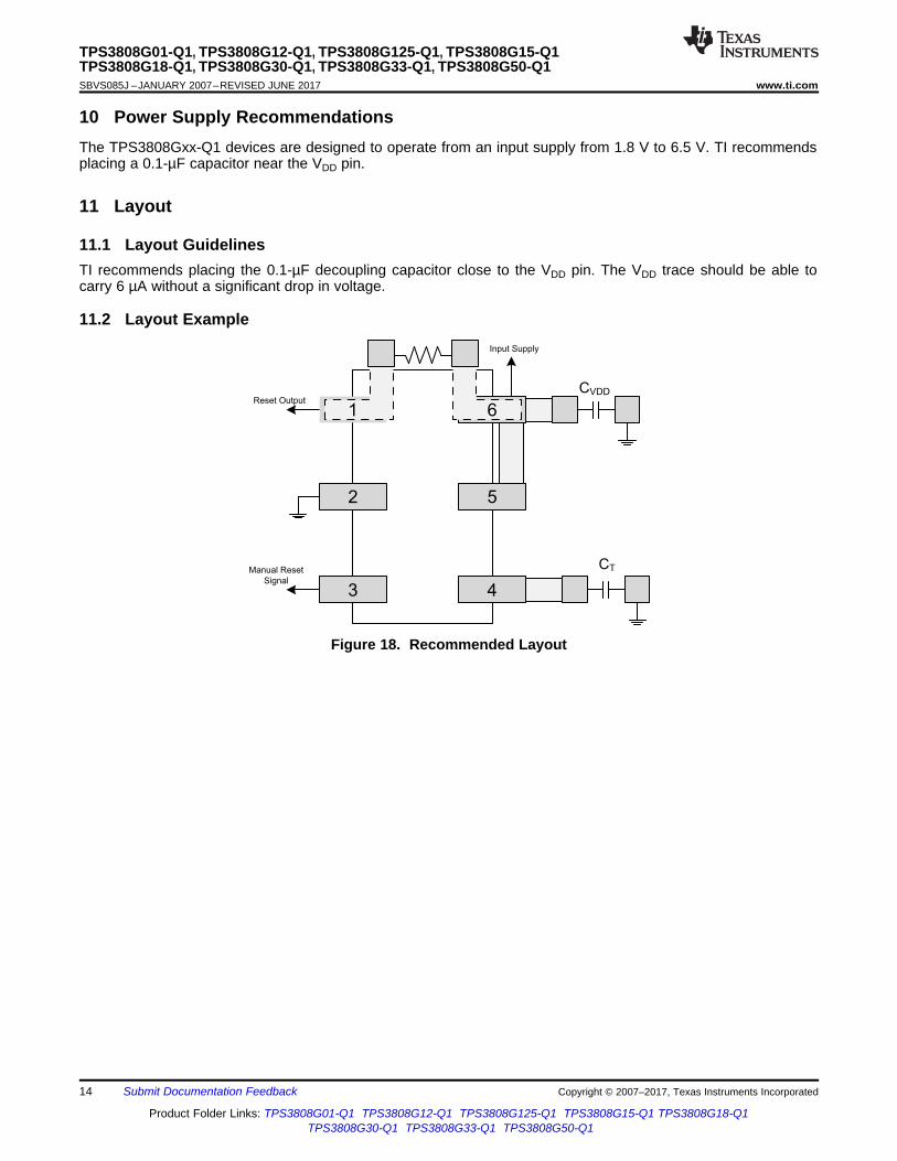
10 Power Supply RecommendationsThe TPS3808Gxx-Q1 devices are designed to operate from an input supply from 1.8 V to 6.5 V. TI recommendsplacing a 0.1-µF capacitor near the VDD pin.
11 Layout
11.1 Layout GuidelinesTI recommends placing the 0.1-µF decoupling capacitor close to the VDD pin. The VDD trace should be able tocarry 6 µA without a significant drop in voltage.
11.2 Layout Example
Figure 18. Recommended Layout
15
TPS3808G01-Q1, TPS3808G12-Q1, TPS3808G125-Q1, TPS3808G15-Q1TPS3808G18-Q1, TPS3808G30-Q1, TPS3808G33-Q1, TPS3808G50-Q1
www.ti.com SBVS085J –JANUARY 2007–REVISED JUNE 2017
Product Folder Links: TPS3808G01-Q1 TPS3808G12-Q1 TPS3808G125-Q1 TPS3808G15-Q1 TPS3808G18-Q1TPS3808G30-Q1 TPS3808G33-Q1 TPS3808G50-Q1
Submit Documentation FeedbackCopyright © 2007–2017, Texas Instruments Incorporated
12 Device and Documentation Support
12.1 Related LinksThe table below lists quick access links. Categories include technical documents, support and communityresources, tools and software, and quick access to sample or buy.
Table 2. Related Links
PARTS PRODUCT FOLDER SAMPLE & BUY TECHNICALDOCUMENTS
TOOLS &SOFTWARE
SUPPORT &COMMUNITY
TPS3808G01-Q1 Click here Click here Click here Click here Click hereTPS3808G12-Q1 Click here Click here Click here Click here Click hereTPS3808G125-Q1 Click here Click here Click here Click here Click hereTPS3808G15-Q1 Click here Click here Click here Click here Click hereTPS3808G18-Q1 Click here Click here Click here Click here Click hereTPS3808G30-Q1 Click here Click here Click here Click here Click hereTPS3808G33-Q1 Click here Click here Click here Click here Click hereTPS3808G50-Q1 Click here Click here Click here Click here Click here
12.2 Receiving Notification of Documentation UpdatesTo receive notification of documentation updates, navigate to the device product folder on ti.com. In the upperright corner, click on Alert me to register and receive a weekly digest of any product information that haschanged. For change details, review the revision history included in any revised document.
12.3 Community ResourcesThe following links connect to TI community resources. Linked contents are provided "AS IS" by the respectivecontributors. They do not constitute TI specifications and do not necessarily reflect TI's views; see TI's Terms ofUse.
TI E2E™ Online Community TI's Engineer-to-Engineer (E2E) Community. Created to foster collaborationamong engineers. At e2e.ti.com, you can ask questions, share knowledge, explore ideas and helpsolve problems with fellow engineers.
Design Support TI's Design Support Quickly find helpful E2E forums along with design support tools andcontact information for technical support.
12.4 TrademarksE2E is a trademark of Texas Instruments.All other trademarks are the property of their respective owners.
12.5 Electrostatic Discharge CautionThese devices have limited built-in ESD protection. The leads should be shorted together or the device placed in conductive foamduring storage or handling to prevent electrostatic damage to the MOS gates.
12.6 GlossarySLYZ022 — TI Glossary.
This glossary lists and explains terms, acronyms, and definitions.
13 Mechanical, Packaging, and Orderable InformationThe following pages include mechanical, packaging, and orderable information. This information is the mostcurrent data available for the designated devices. This data is subject to change without notice and revision ofthis document. For browser-based versions of this data sheet, refer to the left-hand navigation.
PACKAGE OPTION ADDENDUM
www.ti.com 12-Jun-2017
Addendum-Page 1
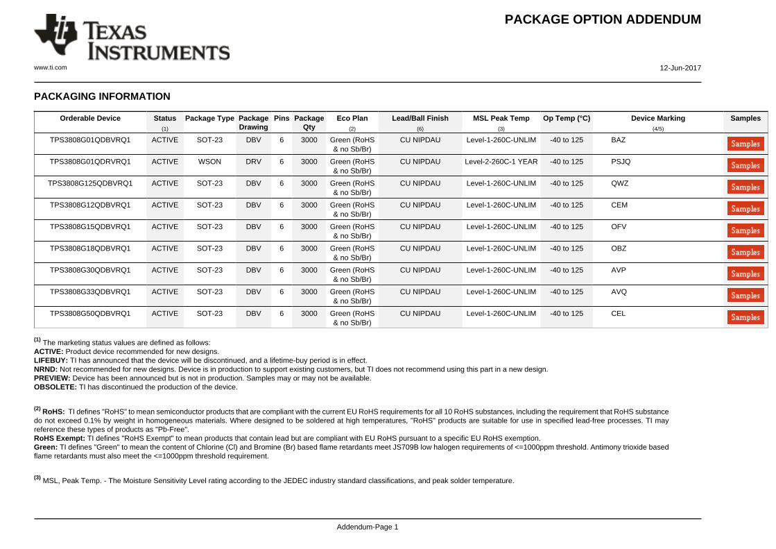
PACKAGING INFORMATION
Orderable Device Status(1)
Package Type PackageDrawing
Pins PackageQty
Eco Plan(2)
Lead/Ball Finish(6)
MSL Peak Temp(3)
Op Temp (°C) Device Marking(4/5)
Samples
TPS3808G01QDBVRQ1 ACTIVE SOT-23 DBV 6 3000 Green (RoHS& no Sb/Br)
CU NIPDAU Level-1-260C-UNLIM -40 to 125 BAZ
TPS3808G01QDRVRQ1 ACTIVE WSON DRV 6 3000 Green (RoHS& no Sb/Br)
CU NIPDAU Level-2-260C-1 YEAR -40 to 125 PSJQ
TPS3808G125QDBVRQ1 ACTIVE SOT-23 DBV 6 3000 Green (RoHS& no Sb/Br)
CU NIPDAU Level-1-260C-UNLIM -40 to 125 QWZ
TPS3808G12QDBVRQ1 ACTIVE SOT-23 DBV 6 3000 Green (RoHS& no Sb/Br)
CU NIPDAU Level-1-260C-UNLIM -40 to 125 CEM
TPS3808G15QDBVRQ1 ACTIVE SOT-23 DBV 6 3000 Green (RoHS& no Sb/Br)
CU NIPDAU Level-1-260C-UNLIM -40 to 125 OFV
TPS3808G18QDBVRQ1 ACTIVE SOT-23 DBV 6 3000 Green (RoHS& no Sb/Br)
CU NIPDAU Level-1-260C-UNLIM -40 to 125 OBZ
TPS3808G30QDBVRQ1 ACTIVE SOT-23 DBV 6 3000 Green (RoHS& no Sb/Br)
CU NIPDAU Level-1-260C-UNLIM -40 to 125 AVP
TPS3808G33QDBVRQ1 ACTIVE SOT-23 DBV 6 3000 Green (RoHS& no Sb/Br)
CU NIPDAU Level-1-260C-UNLIM -40 to 125 AVQ
TPS3808G50QDBVRQ1 ACTIVE SOT-23 DBV 6 3000 Green (RoHS& no Sb/Br)
CU NIPDAU Level-1-260C-UNLIM -40 to 125 CEL
(1) The marketing status values are defined as follows:ACTIVE: Product device recommended for new designs.LIFEBUY: TI has announced that the device will be discontinued, and a lifetime-buy period is in effect.NRND: Not recommended for new designs. Device is in production to support existing customers, but TI does not recommend using this part in a new design.PREVIEW: Device has been announced but is not in production. Samples may or may not be available.OBSOLETE: TI has discontinued the production of the device.
(2) RoHS: TI defines "RoHS" to mean semiconductor products that are compliant with the current EU RoHS requirements for all 10 RoHS substances, including the requirement that RoHS substancedo not exceed 0.1% by weight in homogeneous materials. Where designed to be soldered at high temperatures, "RoHS" products are suitable for use in specified lead-free processes. TI mayreference these types of products as "Pb-Free".RoHS Exempt: TI defines "RoHS Exempt" to mean products that contain lead but are compliant with EU RoHS pursuant to a specific EU RoHS exemption.Green: TI defines "Green" to mean the content of Chlorine (Cl) and Bromine (Br) based flame retardants meet JS709B low halogen requirements of <=1000ppm threshold. Antimony trioxide basedflame retardants must also meet the <=1000ppm threshold requirement.
(3) MSL, Peak Temp. - The Moisture Sensitivity Level rating according to the JEDEC industry standard classifications, and peak solder temperature.
PACKAGE OPTION ADDENDUM
www.ti.com 12-Jun-2017
Addendum-Page 2
(4) There may be additional marking, which relates to the logo, the lot trace code information, or the environmental category on the device.
(5) Multiple Device Markings will be inside parentheses. Only one Device Marking contained in parentheses and separated by a "~" will appear on a device. If a line is indented then it is a continuationof the previous line and the two combined represent the entire Device Marking for that device.
(6) Lead/Ball Finish - Orderable Devices may have multiple material finish options. Finish options are separated by a vertical ruled line. Lead/Ball Finish values may wrap to two lines if the finishvalue exceeds the maximum column width.
Important Information and Disclaimer:The information provided on this page represents TI's knowledge and belief as of the date that it is provided. TI bases its knowledge and belief on informationprovided by third parties, and makes no representation or warranty as to the accuracy of such information. Efforts are underway to better integrate information from third parties. TI has taken andcontinues to take reasonable steps to provide representative and accurate information but may not have conducted destructive testing or chemical analysis on incoming materials and chemicals.TI and TI suppliers consider certain information to be proprietary, and thus CAS numbers and other limited information may not be available for release.
In no event shall TI's liability arising out of such information exceed the total purchase price of the TI part(s) at issue in this document sold by TI to Customer on an annual basis.
OTHER QUALIFIED VERSIONS OF TPS3808-Q1 :
• Catalog: TPS3808
• Enhanced Product: TPS3808-EP
NOTE: Qualified Version Definitions:
• Catalog - TI's standard catalog product
• Enhanced Product - Supports Defense, Aerospace and Medical Applications
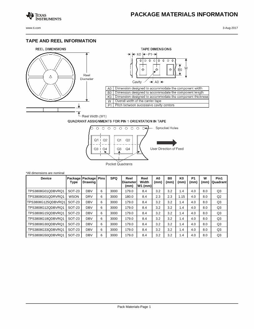
TAPE AND REEL INFORMATION
*All dimensions are nominal
Device PackageType
PackageDrawing
Pins SPQ ReelDiameter
(mm)
ReelWidth
W1 (mm)
A0(mm)
B0(mm)
K0(mm)
P1(mm)
W(mm)
Pin1Quadrant
TPS3808G01QDBVRQ1 SOT-23 DBV 6 3000 179.0 8.4 3.2 3.2 1.4 4.0 8.0 Q3
TPS3808G01QDRVRQ1 WSON DRV 6 3000 180.0 8.4 2.3 2.3 1.15 4.0 8.0 Q2
TPS3808G125QDBVRQ1 SOT-23 DBV 6 3000 179.0 8.4 3.2 3.2 1.4 4.0 8.0 Q3
TPS3808G12QDBVRQ1 SOT-23 DBV 6 3000 179.0 8.4 3.2 3.2 1.4 4.0 8.0 Q3
TPS3808G15QDBVRQ1 SOT-23 DBV 6 3000 179.0 8.4 3.2 3.2 1.4 4.0 8.0 Q3
TPS3808G18QDBVRQ1 SOT-23 DBV 6 3000 179.0 8.4 3.2 3.2 1.4 4.0 8.0 Q3
TPS3808G30QDBVRQ1 SOT-23 DBV 6 3000 179.0 8.4 3.2 3.2 1.4 4.0 8.0 Q3
TPS3808G33QDBVRQ1 SOT-23 DBV 6 3000 179.0 8.4 3.2 3.2 1.4 4.0 8.0 Q3
TPS3808G50QDBVRQ1 SOT-23 DBV 6 3000 179.0 8.4 3.2 3.2 1.4 4.0 8.0 Q3
PACKAGE MATERIALS INFORMATION
www.ti.com 3-Aug-2017
Pack Materials-Page 1
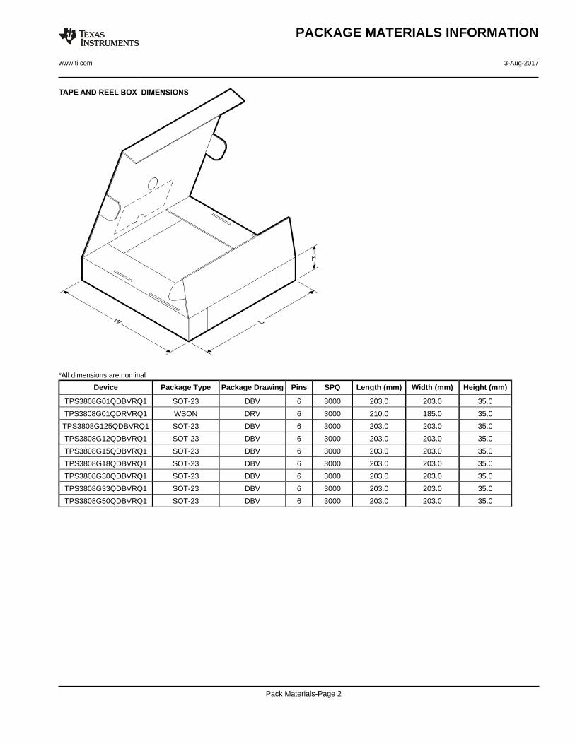
*All dimensions are nominal
Device Package Type Package Drawing Pins SPQ Length (mm) Width (mm) Height (mm)
TPS3808G01QDBVRQ1 SOT-23 DBV 6 3000 203.0 203.0 35.0
TPS3808G01QDRVRQ1 WSON DRV 6 3000 210.0 185.0 35.0
TPS3808G125QDBVRQ1 SOT-23 DBV 6 3000 203.0 203.0 35.0
TPS3808G12QDBVRQ1 SOT-23 DBV 6 3000 203.0 203.0 35.0
TPS3808G15QDBVRQ1 SOT-23 DBV 6 3000 203.0 203.0 35.0
TPS3808G18QDBVRQ1 SOT-23 DBV 6 3000 203.0 203.0 35.0
TPS3808G30QDBVRQ1 SOT-23 DBV 6 3000 203.0 203.0 35.0
TPS3808G33QDBVRQ1 SOT-23 DBV 6 3000 203.0 203.0 35.0
TPS3808G50QDBVRQ1 SOT-23 DBV 6 3000 203.0 203.0 35.0
PACKAGE MATERIALS INFORMATION
www.ti.com 3-Aug-2017
Pack Materials-Page 2
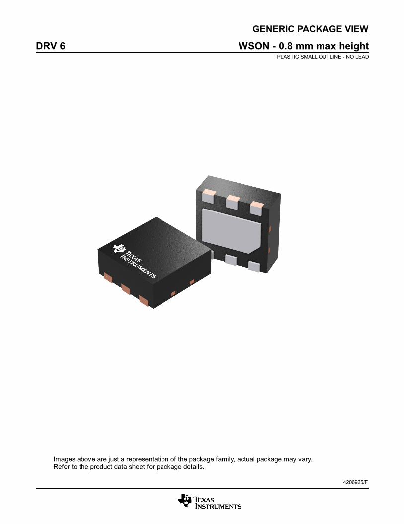
GENERIC PACKAGE VIEW
Images above are just a representation of the package family, actual package may vary.Refer to the product data sheet for package details.
DRV 6 WSON - 0.8 mm max heightPLASTIC SMALL OUTLINE - NO LEAD
4206925/F
www.ti.com
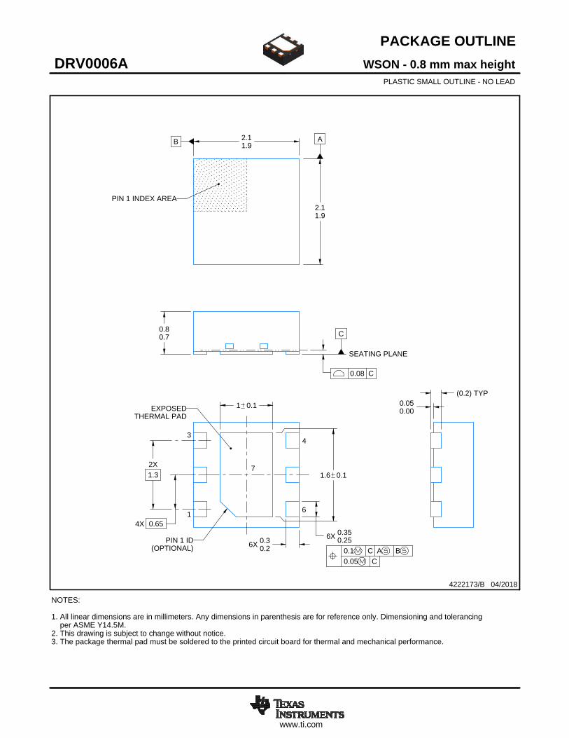
PACKAGE OUTLINE
C
6X 0.350.25
1.6 0.1
6X 0.30.2
2X1.3
1 0.1
4X 0.65
0.80.7
0.050.00
B 2.11.9
A
2.11.9
(0.2) TYP
WSON - 0.8 mm max heightDRV0006APLASTIC SMALL OUTLINE - NO LEAD
4222173/B 04/2018
PIN 1 INDEX AREA
SEATING PLANE
0.08 C
1
34
6
(OPTIONAL)PIN 1 ID
0.1 C A B0.05 C
THERMAL PADEXPOSED
7
NOTES: 1. All linear dimensions are in millimeters. Any dimensions in parenthesis are for reference only. Dimensioning and tolerancing per ASME Y14.5M. 2. This drawing is subject to change without notice. 3. The package thermal pad must be soldered to the printed circuit board for thermal and mechanical performance.
SCALE 5.500
www.ti.com
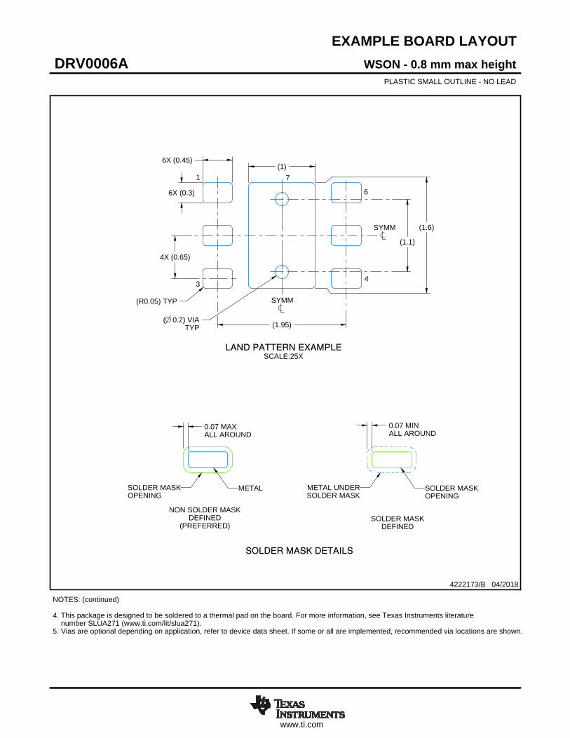
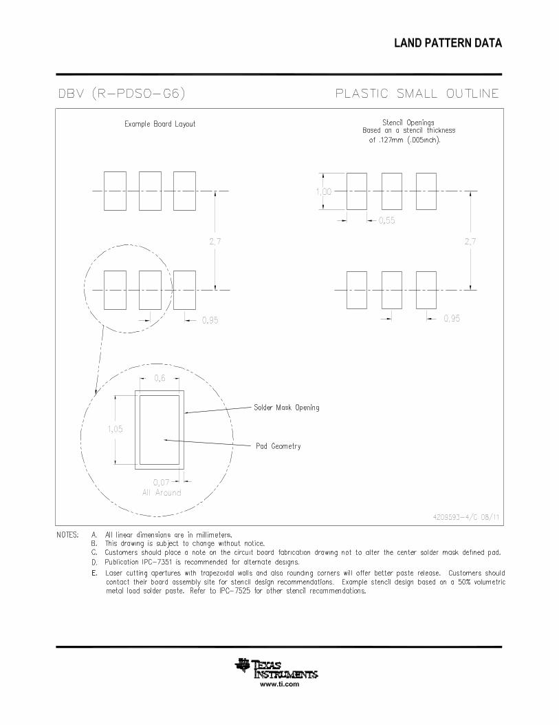
EXAMPLE BOARD LAYOUT
0.07 MINALL AROUND
0.07 MAXALL AROUND
(1)
4X (0.65)
(1.95)
6X (0.3)
6X (0.45)
(1.6)
(R0.05) TYP
( 0.2) VIATYP
(1.1)
WSON - 0.8 mm max heightDRV0006APLASTIC SMALL OUTLINE - NO LEAD
4222173/B 04/2018
SYMM
1
34
6
SYMM
LAND PATTERN EXAMPLESCALE:25X
7
NOTES: (continued) 4. This package is designed to be soldered to a thermal pad on the board. For more information, see Texas Instruments literature number SLUA271 (www.ti.com/lit/slua271).5. Vias are optional depending on application, refer to device data sheet. If some or all are implemented, recommended via locations are shown.
SOLDER MASKOPENINGSOLDER MASK
METAL UNDER
SOLDER MASKDEFINED
METALSOLDER MASKOPENING
SOLDER MASK DETAILS
NON SOLDER MASKDEFINED
(PREFERRED)
www.ti.com
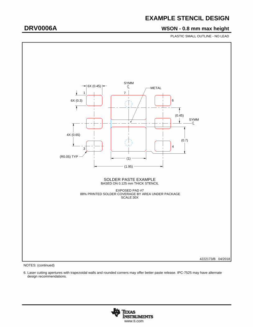
EXAMPLE STENCIL DESIGN
6X (0.3)
6X (0.45)
4X (0.65)
(0.7)
(1)
(1.95)
(R0.05) TYP
(0.45)
WSON - 0.8 mm max heightDRV0006APLASTIC SMALL OUTLINE - NO LEAD
4222173/B 04/2018
NOTES: (continued) 6. Laser cutting apertures with trapezoidal walls and rounded corners may offer better paste release. IPC-7525 may have alternate design recommendations.
SOLDER PASTE EXAMPLEBASED ON 0.125 mm THICK STENCIL
EXPOSED PAD #7
88% PRINTED SOLDER COVERAGE BY AREA UNDER PACKAGESCALE:30X
SYMM
1
3 4
6
SYMM
METAL7
IMPORTANT NOTICE
Texas Instruments Incorporated (TI) reserves the right to make corrections, enhancements, improvements and other changes to itssemiconductor products and services per JESD46, latest issue, and to discontinue any product or service per JESD48, latest issue. Buyersshould obtain the latest relevant information before placing orders and should verify that such information is current and complete.TI’s published terms of sale for semiconductor products (http://www.ti.com/sc/docs/stdterms.htm) apply to the sale of packaged integratedcircuit products that TI has qualified and released to market. Additional terms may apply to the use or sale of other types of TI products andservices.Reproduction of significant portions of TI information in TI data sheets is permissible only if reproduction is without alteration and isaccompanied by all associated warranties, conditions, limitations, and notices. TI is not responsible or liable for such reproduceddocumentation. Information of third parties may be subject to additional restrictions. Resale of TI products or services with statementsdifferent from or beyond the parameters stated by TI for that product or service voids all express and any implied warranties for theassociated TI product or service and is an unfair and deceptive business practice. TI is not responsible or liable for any such statements.Buyers and others who are developing systems that incorporate TI products (collectively, “Designers”) understand and agree that Designersremain responsible for using their independent analysis, evaluation and judgment in designing their applications and that Designers havefull and exclusive responsibility to assure the safety of Designers' applications and compliance of their applications (and of all TI productsused in or for Designers’ applications) with all applicable regulations, laws and other applicable requirements. Designer represents that, withrespect to their applications, Designer has all the necessary expertise to create and implement safeguards that (1) anticipate dangerousconsequences of failures, (2) monitor failures and their consequences, and (3) lessen the likelihood of failures that might cause harm andtake appropriate actions. Designer agrees that prior to using or distributing any applications that include TI products, Designer willthoroughly test such applications and the functionality of such TI products as used in such applications.TI’s provision of technical, application or other design advice, quality characterization, reliability data or other services or information,including, but not limited to, reference designs and materials relating to evaluation modules, (collectively, “TI Resources”) are intended toassist designers who are developing applications that incorporate TI products; by downloading, accessing or using TI Resources in anyway, Designer (individually or, if Designer is acting on behalf of a company, Designer’s company) agrees to use any particular TI Resourcesolely for this purpose and subject to the terms of this Notice.TI’s provision of TI Resources does not expand or otherwise alter TI’s applicable published warranties or warranty disclaimers for TIproducts, and no additional obligations or liabilities arise from TI providing such TI Resources. TI reserves the right to make corrections,enhancements, improvements and other changes to its TI Resources. TI has not conducted any testing other than that specificallydescribed in the published documentation for a particular TI Resource.Designer is authorized to use, copy and modify any individual TI Resource only in connection with the development of applications thatinclude the TI product(s) identified in such TI Resource. NO OTHER LICENSE, EXPRESS OR IMPLIED, BY ESTOPPEL OR OTHERWISETO ANY OTHER TI INTELLECTUAL PROPERTY RIGHT, AND NO LICENSE TO ANY TECHNOLOGY OR INTELLECTUAL PROPERTYRIGHT OF TI OR ANY THIRD PARTY IS GRANTED HEREIN, including but not limited to any patent right, copyright, mask work right, orother intellectual property right relating to any combination, machine, or process in which TI products or services are used. Informationregarding or referencing third-party products or services does not constitute a license to use such products or services, or a warranty orendorsement thereof. Use of TI Resources may require a license from a third party under the patents or other intellectual property of thethird party, or a license from TI under the patents or other intellectual property of TI.TI RESOURCES ARE PROVIDED “AS IS” AND WITH ALL FAULTS. TI DISCLAIMS ALL OTHER WARRANTIES ORREPRESENTATIONS, EXPRESS OR IMPLIED, REGARDING RESOURCES OR USE THEREOF, INCLUDING BUT NOT LIMITED TOACCURACY OR COMPLETENESS, TITLE, ANY EPIDEMIC FAILURE WARRANTY AND ANY IMPLIED WARRANTIES OFMERCHANTABILITY, FITNESS FOR A PARTICULAR PURPOSE, AND NON-INFRINGEMENT OF ANY THIRD PARTY INTELLECTUALPROPERTY RIGHTS. TI SHALL NOT BE LIABLE FOR AND SHALL NOT DEFEND OR INDEMNIFY DESIGNER AGAINST ANY CLAIM,INCLUDING BUT NOT LIMITED TO ANY INFRINGEMENT CLAIM THAT RELATES TO OR IS BASED ON ANY COMBINATION OFPRODUCTS EVEN IF DESCRIBED IN TI RESOURCES OR OTHERWISE. IN NO EVENT SHALL TI BE LIABLE FOR ANY ACTUAL,DIRECT, SPECIAL, COLLATERAL, INDIRECT, PUNITIVE, INCIDENTAL, CONSEQUENTIAL OR EXEMPLARY DAMAGES INCONNECTION WITH OR ARISING OUT OF TI RESOURCES OR USE THEREOF, AND REGARDLESS OF WHETHER TI HAS BEENADVISED OF THE POSSIBILITY OF SUCH DAMAGES.Unless TI has explicitly designated an individual product as meeting the requirements of a particular industry standard (e.g., ISO/TS 16949and ISO 26262), TI is not responsible for any failure to meet such industry standard requirements.Where TI specifically promotes products as facilitating functional safety or as compliant with industry functional safety standards, suchproducts are intended to help enable customers to design and create their own applications that meet applicable functional safety standardsand requirements. Using products in an application does not by itself establish any safety features in the application. Designers mustensure compliance with safety-related requirements and standards applicable to their applications. Designer may not use any TI products inlife-critical medical equipment unless authorized officers of the parties have executed a special contract specifically governing such use.Life-critical medical equipment is medical equipment where failure of such equipment would cause serious bodily injury or death (e.g., lifesupport, pacemakers, defibrillators, heart pumps, neurostimulators, and implantables). Such equipment includes, without limitation, allmedical devices identified by the U.S. Food and Drug Administration as Class III devices and equivalent classifications outside the U.S.TI may expressly designate certain products as completing a particular qualification (e.g., Q100, Military Grade, or Enhanced Product).Designers agree that it has the necessary expertise to select the product with the appropriate qualification designation for their applicationsand that proper product selection is at Designers’ own risk. Designers are solely responsible for compliance with all legal and regulatoryrequirements in connection with such selection.Designer will fully indemnify TI and its representatives against any damages, costs, losses, and/or liabilities arising out of Designer’s non-compliance with the terms and provisions of this Notice.
Mailing Address: Texas Instruments, Post Office Box 655303, Dallas, Texas 75265Copyright © 2018, Texas Instruments Incorporated