TPA3200D1 Audio Power Amplifier Evaluation Module Sheets/Texas Instruments PDFs... · TPA3200D1...
13
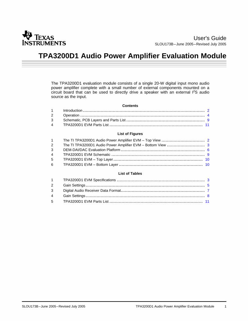
User's Guide SLOU173B – June 2005 – Revised July 2005 TPA3200D1 Audio Power Amplifier Evaluation Module The TPA3200D1 evaluation module consists of a single 20-W digital input mono audio power amplifier complete with a small number of external components mounted on a circuit board that can be used to directly drive a speaker with an external I 2 S audio source as the input. Contents 1 Introduction .......................................................................................... 2 2 Operation ............................................................................................ 4 3 Schematic, PCB Layers and Parts List .......................................................... 9 4 TPA3200D1 EVM Parts List ..................................................................... 11 List of Figures 1 The TI TPA3200D1 Audio Power Amplifier EVM – Top View ................................ 2 2 The TI TPA3200D1 Audio Power Amplifier EVM – Bottom View ............................ 3 3 DEM-DAI/DAC Evaluation Platform .............................................................. 6 4 TPA3200D1 EVM Schematic ..................................................................... 9 5 TPA3200D1 EVM – Top Layer .................................................................. 10 6 TPA3200D1 EVM – Bottom Layer .............................................................. 10 List of Tables 1 TPA3200D1 EVM Specifications ................................................................. 3 2 Gain Settings ........................................................................................ 5 3 Digital Audio Receiver Data Format.............................................................. 7 4 Gain Settings ........................................................................................ 8 5 TPA3200D1 EVM Parts List ..................................................................... 11 SLOU173B – June 2005 – Revised July 2005 TPA3200D1 Audio Power Amplifier Evaluation Module 1
Transcript of TPA3200D1 Audio Power Amplifier Evaluation Module Sheets/Texas Instruments PDFs... · TPA3200D1...
User's GuideSLOU173B–June 2005–Revised July 2005
TPA3200D1 Audio Power Amplifier Evaluation Module
The TPA3200D1 evaluation module consists of a single 20-W digital input mono audiopower amplifier complete with a small number of external components mounted on acircuit board that can be used to directly drive a speaker with an external I2S audiosource as the input.
Contents1 Introduction .......................................................................................... 22 Operation ............................................................................................ 43 Schematic, PCB Layers and Parts List .......................................................... 94 TPA3200D1 EVM Parts List ..................................................................... 11
List of Figures
1 The TI TPA3200D1 Audio Power Amplifier EVM – Top View ................................ 22 The TI TPA3200D1 Audio Power Amplifier EVM – Bottom View ............................ 33 DEM-DAI/DAC Evaluation Platform .............................................................. 64 TPA3200D1 EVM Schematic ..................................................................... 95 TPA3200D1 EVM – Top Layer .................................................................. 106 TPA3200D1 EVM – Bottom Layer .............................................................. 10
List of Tables
1 TPA3200D1 EVM Specifications ................................................................. 32 Gain Settings ........................................................................................ 53 Digital Audio Receiver Data Format.............................................................. 74 Gain Settings ........................................................................................ 8
5 TPA3200D1 EVM Parts List ..................................................................... 11
SLOU173B–June 2005–Revised July 2005 TPA3200D1 Audio Power Amplifier Evaluation Module 1
www.ti.com
1 Introduction
Introduction
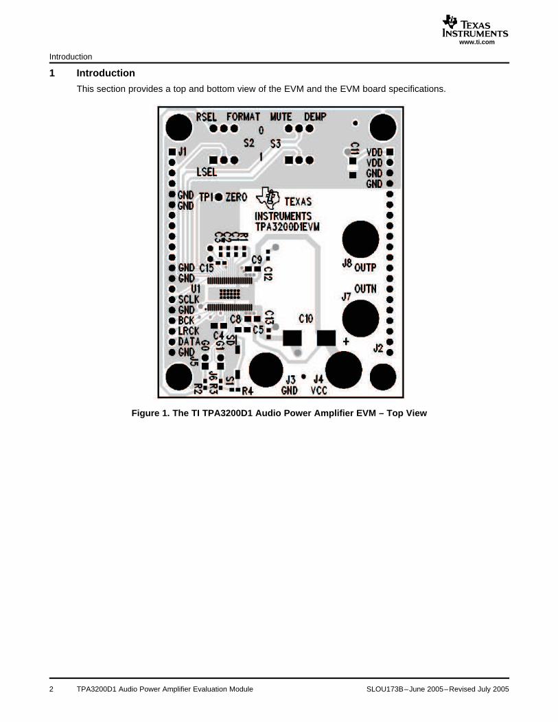
This section provides a top and bottom view of the EVM and the EVM board specifications.
Figure 1. The TI TPA3200D1 Audio Power Amplifier EVM – Top View
TPA3200D1 Audio Power Amplifier Evaluation Module2 SLOU173B–June 2005–Revised July 2005
www.ti.com
Introduction
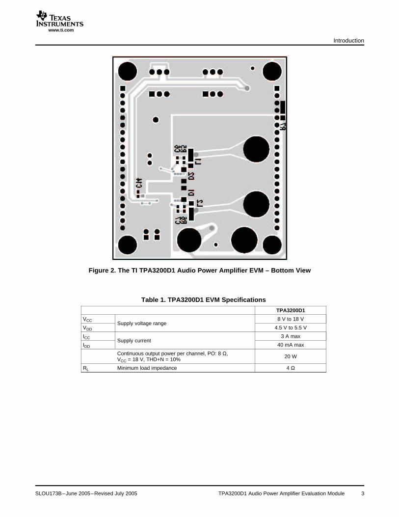
Figure 2. The TI TPA3200D1 Audio Power Amplifier EVM – Bottom View
Table 1. TPA3200D1 EVM Specifications
TPA3200D1
VCC 8 V to 18 VSupply voltage range
VDD 4.5 V to 5.5 V
ICC 3 A maxSupply current
IDD 40 mA max
Continuous output power per channel, PO: 8 Ω, 20 WVCC = 18 V, THD+N = 10%
RL Minimum load impedance 4 Ω
SLOU173B–June 2005–Revised July 2005 TPA3200D1 Audio Power Amplifier Evaluation Module 3
www.ti.com
2 Operation
2.1 Quick Start List for Stand-Alone Operation
Operation
To use the TPA3200D1EVM stand-alone or when connecting it into existing circuits or equipment, followthese steps. Connections to the EVM module can be made by inserting stripped wire into the platedthrough holes on the J1, J2 headers and using banana plugs for the other connectors on the PCB.
2.1.1 Power Supply (Step 1)1. Ensure that all external power sources are set to OFF.2. Connect an additional external regulated power supply set to 5 V to the module VDD and GND pins on
the top side of the J2 header.
Note:
This supply should be turned ON before the VCC supply is turned ON.
3. Connect an external regulated power supply adjusted from 8 V–18 V to the module VCC (J4) and GND(J3) banana jacks taking care to observe marked polarity.
2.1.2 Evaluation Module Preparations (Step 2)
Inputs and Outputs1. Ensure that all connections are made to the I2S inputs (SCLK, BCK, LRCK, DATA, and GND) on the
J1 header.2. Connect a speaker across OUTP (J8) and OUTN (J7)3. Install both gain jumpers GAIN0 (J5) and GAIN1 (J6). This sets the gain of the amplifier to the lowest
level, 12 dB.
Control Inputs1. SHUTDOWN: This terminal is active low. A low on the device terminal (< 0.8 V) shuts down the
amplifier; a high (> 2 V) on the device terminal places the amplifier in the active state. Holding downswitch S1 places the amplifier in the SHUTDOWN state. Releasing S1 returns the amplifier to theactive state.
2. MUTE: This terminal is active high. A high on this terminal immediately terminates audio playbackthrough the speakers. However, the outputs are still active (they are switching). The outputs are notdisabled like the SHUTDOWN case. S3 on the EVM controls the state of the MUTE terminal. Switchingthe left side of S3 to 1 turns Mute on. Switching S3 to the 0 position turns Mute off.
3. FORMAT: This terminal selects between two possible digital data input formats. S2 on the EVMcontrols the data format. Switching the right side of S2 to 0 selects the 16-24 bit, I2S format. Switchingthe right side of S2 to 1 selects the 16-bit right-justified format.
4. LSEL/RSEL: A typical digital input data stream consists of 2 channels of data. However, this amplifieris a mono, bridged-tied amplifier. Therefore, it is necessary to select which channel of data is sent tothe mono output. This terminal is used to select between the 2 channels, typically left/right data.Switching the left side of S2 to the RSEL position selects right-channel data. Switching the left side ofS2 to the LSEL position selects left-channel data.
5. DEMP: This terminal is used to enable/disable the internal 44.1-kHz de-emphasis filter. S3 on the EVMcontrols the functionality of this terminal. Switching the right side of S3 to the 0 position disables the44.1-kHz de-emphasis. Switching the right side of S3 to the 1 position enables the 44.1-kHzde-emphasis.
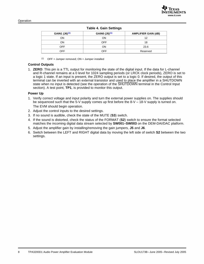
6. GAIN0/GAIN1: Together, these terminals control the back-end gain of the amplifier. Jumpers J5 andJ6 control these terminals. The position of these jumpers and resulting gain is shown in Table 2.
4 TPA3200D1 Audio Power Amplifier Evaluation Module SLOU173B–June 2005–Revised July 2005
www.ti.com
Operation
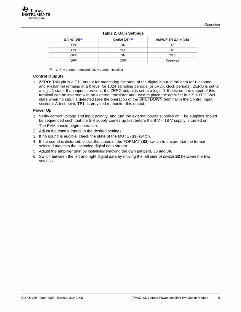
Table 2. Gain Settings
GAIN1 (J6) (1) GAIN0 (J5) (1) AMPLIFIER GAIN (dB)
ON ON 12
ON OFF 18
OFF ON 23.6
OFF OFF Reserved
(1) OFF = Jumper removed; ON = Jumper installed
Control Outputs1. ZERO: This pin is a TTL output for monitoring the state of the digital input. If the data for L-channel
and R-channel remains at a 0 level for 1024 sampling periods (or LRCK clock periods), ZERO is set toa logic 1 state. If an input is present, the ZERO output is set to a logic 0. If desired, the output of thisterminal can be inverted with an external transistor and used to place the amplifier in a SHUTDOWNstate when no input is detected (see the operation of the SHUTDOWN terminal in the Control Inputsection). A test point, TP1, is provided to monitor this output.
Power Up1. Verify correct voltage and input polarity, and turn the external power supplies on. The supplies should
be sequenced such that the 5-V supply comes up first before the 8-V – 18-V supply is turned on.The EVM should begin operation.
2. Adjust the control inputs to the desired settings.3. If no sound is audible, check the state of the MUTE (S3) switch.4. If the sound is distorted, check the status of the FORMAT (S2) switch to ensure that the format
selected matches the incoming digital data stream.5. Adjust the amplifier gain by installing/removing the gain jumpers, J5 and J6.6. Switch between the left and right digital data by moving the left side of switch S2 between the two
settings.
SLOU173B–June 2005–Revised July 2005 TPA3200D1 Audio Power Amplifier Evaluation Module 5
www.ti.com
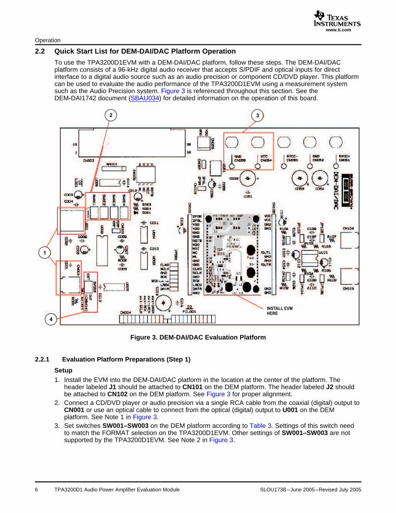
2.2 Quick Start List for DEM-DAI/DAC Platform Operation
INSTALL EVM
HERE
3
1
4
2
Operation
To use the TPA3200D1EVM with a DEM-DAI/DAC platform, follow these steps. The DEM-DAI/DACplatform consists of a 96-kHz digital audio receiver that accepts S/PDIF and optical inputs for directinterface to a digital audio source such as an audio precision or component CD/DVD player. This platformcan be used to evaluate the audio performance of the TPA3200D1EVM using a measurement systemsuch as the Audio Precision system. Figure 3 is referenced throughout this section. See theDEM-DAI1742 document (SBAU034) for detailed information on the operation of this board.
Figure 3. DEM-DAI/DAC Evaluation Platform
2.2.1 Evaluation Platform Preparations (Step 1)
Setup1. Install the EVM into the DEM-DAI/DAC platform in the location at the center of the platform. The
header labeled J1 should be attached to CN101 on the DEM platform. The header labeled J2 shouldbe attached to CN102 on the DEM platform. See Figure 3 for proper alignment.
2. Connect a CD/DVD player or audio precision via a single RCA cable from the coaxial (digital) output toCN001 or use an optical cable to connect from the optical (digital) output to U001 on the DEMplatform. See Note 1 in Figure 3.
3. Set switches SW001–SW003 on the DEM platform according to Table 3. Settings of this switch needto match the FORMAT selection on the TPA3200D1EVM. Other settings of SW001–SW003 are notsupported by the TPA3200D1EVM. See Note 2 in Figure 3.
6 TPA3200D1 Audio Power Amplifier Evaluation Module SLOU173B–June 2005–Revised July 2005
www.ti.com
Operation
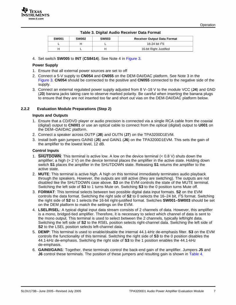
Table 3. Digital Audio Receiver Data Format
SW001 SW002 SW003 Receiver Output Data Format
L H L 16-24 bit I2S
H L H 16-bit Right Justified
4. Set switch SW005 to INT (CS8414). See Note 4 in Figure 3.
Power Supply1. Ensure that all external power sources are set to off2. Connect a 5-V supply to CN054 and CN055 on the DEM-DAI/DAC platform. See Note 3 in the
Figure 3. CN054 should be connected to the positive and CN055 connected to the negative side of thesupply.
3. Connect an external regulated power supply adjusted from 8 V–18 V to the module VCC (J4) and GND(J3) banana jacks taking care to observe marked polarity. Be careful when inserting the banana plugsto ensure that they are not inserted too far and short out vias on the DEM-DAI/DAC platform below.
2.2.2 Evaluation Module Preparations (Step 2)
Inputs and Outputs1. Ensure that a CD/DVD player or audio precision is connected via a single RCA cable from the coaxial
(digital) output to CN001 or use an optical cable to connect from the optical (digital) output to U001 onthe DEM–DAI/DAC platform.
2. Connect a speaker across OUTP (J8) and OUTN (J7) on the TPA3200D1EVM.3. Install both gain jumpers GAIN0 (J5) and GAIN1 (J6) on the TPA3200D1EVM. This sets the gain of
the amplifier to the lowest level, 12 dB.
Control Inputs1. SHUTDOWN: This terminal is active low. A low on the device terminal (< 0.8 V) shuts down the
amplifier; a high (> 2 V) on the device terminal places the amplifier in the active state. Holding downswitch S1 places the amplifier in the SHUTDOWN state. Releasing S1 returns the amplifier to theactive state.
2. MUTE: This terminal is active high. A high on this terminal immediately terminates audio playbackthrough the speakers. However, the outputs are still active (they are switching). The outputs are notdisabled like the SHUTDOWN case above. S3 on the EVM controls the state of the MUTE terminal.Switching the left side of S3 to 1 turns Mute on. Switching S3 to the 0 position turns Mute off.
3. FORMAT: This terminal selects between two possible digital data input formats. S2 on the EVMcontrols the data format. Switching the right side of S2 to 0 selects the 16–24 bit, I2S format. Switchingthe right side of S2 to 1 selects the 16-bit right-justified format. Switches SW001–SW003 should be seton the DEM platform to match the settings on the EVM.
4. LSEL/RSEL: A typical digital input data stream consists of 2 channels of data. However, this amplifieris a mono, bridged-tied amplifier. Therefore, it is necessary to select which channel of data is sent tothe mono output. This terminal is used to select between the 2 channels, typically left/right data.Switching the left side of S2 to the RSEL position selects right-channel data. Switching the left side ofS2 to the LSEL position selects left-channel data.
5. DEMP: This terminal is used to enable/disable the internal 44.1-kHz de-emphasis filter. S3 on the EVMcontrols the functionality of this terminal. Switching the right side of S3 to the 0 position disables the44.1-kHz de-emphasis. Switching the right side of S3 to the 1 position enables the 44.1-kHzde-emphasis.
6. GAIN0/GAIN1: Together, these terminals control the back-end gain of the amplifier. Jumpers J5 andJ6 control these terminals. The position of these jumpers and resulting gain is shown in Table 4.
SLOU173B–June 2005–Revised July 2005 TPA3200D1 Audio Power Amplifier Evaluation Module 7
www.ti.com
Operation
Table 4. Gain Settings
GAIN1 (J6) (1) GAIN0 (J5) (1) AMPLIFIER GAIN (dB)
ON ON 12
ON OFF 18
OFF ON 23.6
OFF OFF Reserved
(1) OFF = Jumper removed; ON = Jumper installed
Control Outputs1. ZERO: This pin is a TTL output for monitoring the state of the digital input. If the data for L-channel
and R-channel remains at a 0 level for 1024 sampling periods (or LRCK clock periods), ZERO is set toa logic 1 state. If an input is present, the ZERO output is set to a logic 0. If desired, the output of thisterminal can be inverted with an external transistor and used to place the amplifier in a SHUTDOWNstate when no input is detected (see the operation of the SHUTDOWN terminal in the Control Inputsection). A test point, TP1, is provided to monitor this output.
Power Up1. Verify correct voltage and input polarity and turn the external power supplies on. The supplies should
be sequenced such that the 5-V supply comes up first before the 8-V – 18-V supply is turned on.The EVM should begin operation.
2. Adjust the control inputs to the desired settings.3. If no sound is audible, check the state of the MUTE (S3) switch.4. If the sound is distorted, check the status of the FORMAT (S2) switch to ensure the format selected
matches the incoming digital data stream selected by SW001–SW003 on the DEM-DAI/DAC platform.5. Adjust the amplifier gain by installing/removing the gain jumpers, J5 and J6.6. Switch between the LEFT and RIGHT digital data by moving the left side of switch S2 between the two
settings.
TPA3200D1 Audio Power Amplifier Evaluation Module8 SLOU173B–June 2005–Revised July 2005
www.ti.com
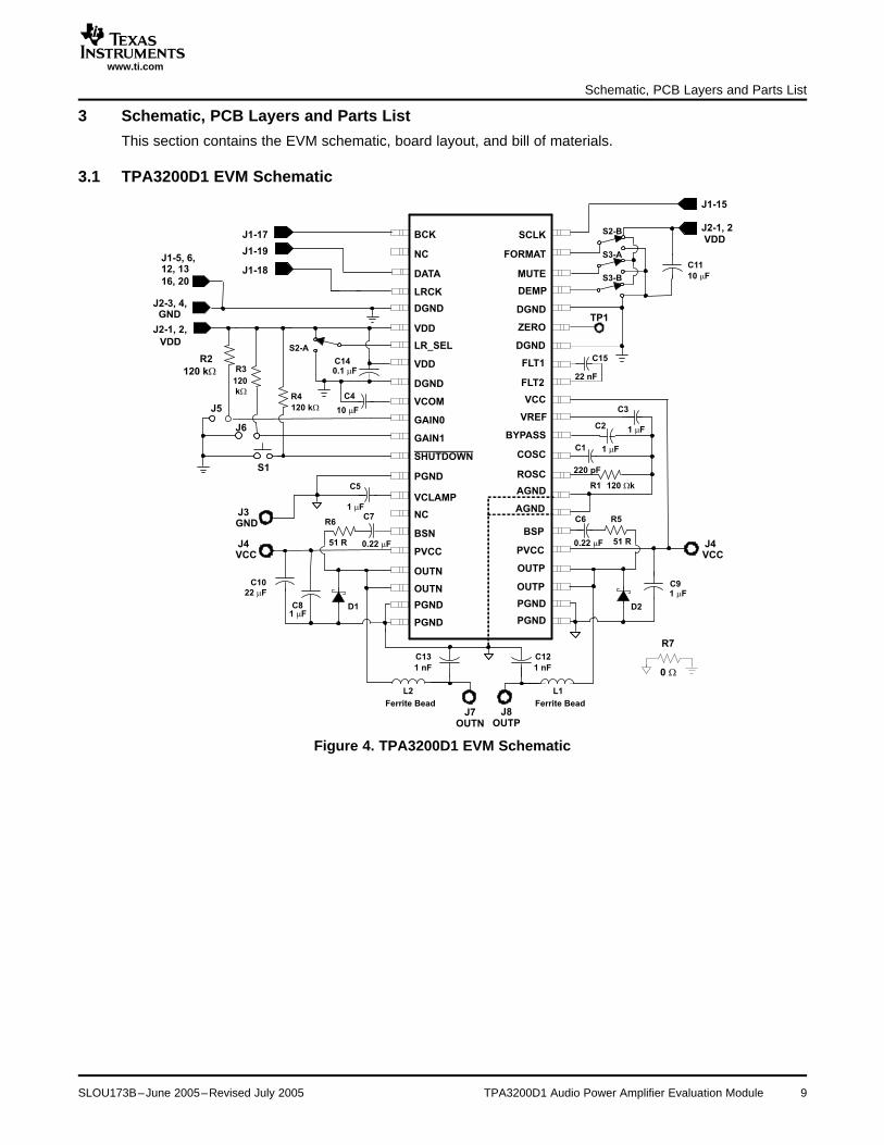
3 Schematic, PCB Layers and Parts List
3.1 TPA3200D1 EVM Schematic
LRCK
DGND
BCK
GAIN0
VCOM
DATA
FORMAT
SCLK
GAIN1
LR_SEL
VDD
NC
DGND
VDD
SHUTDOWN
PGND
PGND
VCLAMP
BSN
OUTN
OUTN
PGND
PVCC
NC
COSC
PGND
PGND
AGND
BSP
OUTP
OUTP
ROSC
PVCC
AGND
MUTE
DGND
DEMP
DGND
FLT1
ZERO
FLT2
VCC
VREF
BYPASS
0.1 Fm
10 Fm
220 pF
R2
J1-17
J1-19
J1-18
J1-5, 6,
J2-3, 4,
12, 13
16, 20
GND
J2-1, 2,
VDD
J3
J7OUTN
J8OUTP
GND
J4VCC
S2-A
120 kW120
kW
R3
R4
120 kWJ5
J6
S1
C14
C4
1 Fm
1 Fm
1 Fm
C5
C7
0.22 Fm 0.22 Fm
22 Fm
R6
51 R
C10
C8
C13
D1 D2
1 nF
C12
1 nF
L2 L1
Ferrite Bead Ferrite Bead
R7
0 W
C9
J4VCC
R5
51 R
C6
R1 120 kW
C1
C3
1 Fm
1 Fm
C15
22 nF
TP1
C11
10 Fm
J1-15
J2-1, 2
VDDS2-B
S3-A
S3-B
C2
Schematic, PCB Layers and Parts List
This section contains the EVM schematic, board layout, and bill of materials.
Figure 4. TPA3200D1 EVM Schematic
SLOU173B–June 2005–Revised July 2005 TPA3200D1 Audio Power Amplifier Evaluation Module 9
www.ti.com
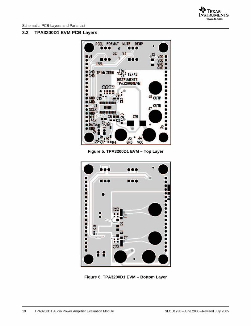
3.2 TPA3200D1 EVM PCB Layers
Schematic, PCB Layers and Parts List
Figure 5. TPA3200D1 EVM – Top Layer
Figure 6. TPA3200D1 EVM – Bottom Layer
TPA3200D1 Audio Power Amplifier Evaluation Module10 SLOU173B–June 2005–Revised July 2005
www.ti.com
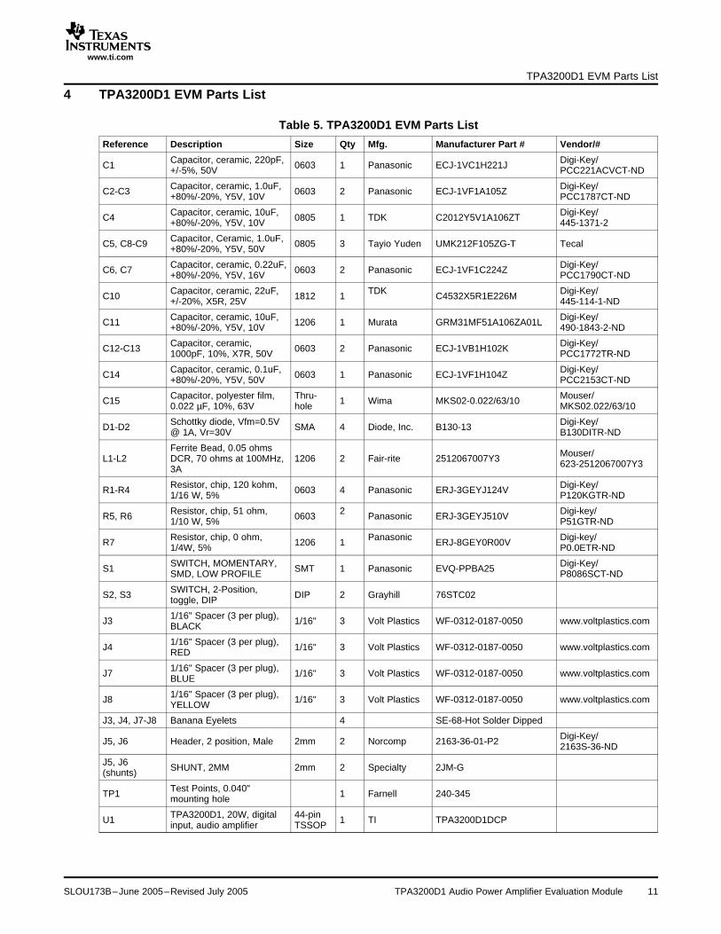
4 TPA3200D1 EVM Parts ListTPA3200D1 EVM Parts List
Table 5. TPA3200D1 EVM Parts List
Reference Description Size Qty Mfg. Manufacturer Part # Vendor/#
Capacitor, ceramic, 220pF, Digi-Key/C1 0603 1 Panasonic ECJ-1VC1H221J+/-5%, 50V PCC221ACVCT-ND
Capacitor, ceramic, 1.0uF, Digi-Key/C2-C3 0603 2 Panasonic ECJ-1VF1A105Z+80%/-20%, Y5V, 10V PCC1787CT-ND
Capacitor, ceramic, 10uF, Digi-Key/C4 0805 1 TDK C2012Y5V1A106ZT+80%/-20%, Y5V, 10V 445-1371-2
Capacitor, Ceramic, 1.0uF,C5, C8-C9 0805 3 Tayio Yuden UMK212F105ZG-T Tecal+80%/-20%, Y5V, 50V
Capacitor, ceramic, 0.22uF, Digi-Key/C6, C7 0603 2 Panasonic ECJ-1VF1C224Z+80%/-20%, Y5V, 16V PCC1790CT-ND
Capacitor, ceramic, 22uF, TDK Digi-Key/C10 1812 1 C4532X5R1E226M+/-20%, X5R, 25V 445-114-1-ND
Capacitor, ceramic, 10uF, Digi-Key/C11 1206 1 Murata GRM31MF51A106ZA01L+80%/-20%, Y5V, 10V 490-1843-2-ND
Capacitor, ceramic, Digi-Key/C12-C13 0603 2 Panasonic ECJ-1VB1H102K1000pF, 10%, X7R, 50V PCC1772TR-ND
Capacitor, ceramic, 0.1uF, Digi-Key/C14 0603 1 Panasonic ECJ-1VF1H104Z+80%/-20%, Y5V, 50V PCC2153CT-ND
Capacitor, polyester film, Thru- Mouser/C15 1 Wima MKS02-0.022/63/100.022 µF, 10%, 63V hole MKS02.022/63/10
Schottky diode, Vfm=0.5V Digi-Key/D1-D2 SMA 4 Diode, Inc. B130-13@ 1A, Vr=30V B130DITR-ND
Ferrite Bead, 0.05 ohms Mouser/L1-L2 DCR, 70 ohms at 100MHz, 1206 2 Fair-rite 2512067007Y3 623-2512067007Y33A
Resistor, chip, 120 kohm, Digi-Key/R1-R4 0603 4 Panasonic ERJ-3GEYJ124V1/16 W, 5% P120KGTR-ND
Resistor, chip, 51 ohm, 2 Digi-key/R5, R6 0603 Panasonic ERJ-3GEYJ510V1/10 W, 5% P51GTR-ND
Resistor, chip, 0 ohm, Panasonic Digi-key/R7 1206 1 ERJ-8GEY0R00V1/4W, 5% P0.0ETR-ND
SWITCH, MOMENTARY, Digi-Key/S1 SMT 1 Panasonic EVQ-PPBA25SMD, LOW PROFILE P8086SCT-ND
SWITCH, 2-Position,S2, S3 DIP 2 Grayhill 76STC02toggle, DIP
1/16" Spacer (3 per plug),J3 1/16" 3 Volt Plastics WF-0312-0187-0050 www.voltplastics.comBLACK
1/16" Spacer (3 per plug),J4 1/16" 3 Volt Plastics WF-0312-0187-0050 www.voltplastics.comRED
1/16" Spacer (3 per plug),J7 1/16" 3 Volt Plastics WF-0312-0187-0050 www.voltplastics.comBLUE
1/16" Spacer (3 per plug),J8 1/16" 3 Volt Plastics WF-0312-0187-0050 www.voltplastics.comYELLOW
J3, J4, J7-J8 Banana Eyelets 4 SE-68-Hot Solder Dipped
Digi-Key/J5, J6 Header, 2 position, Male 2mm 2 Norcomp 2163-36-01-P2 2163S-36-ND
J5, J6 SHUNT, 2MM 2mm 2 Specialty 2JM-G(shunts)
Test Points, 0.040"TP1 1 Farnell 240-345mounting hole
TPA3200D1, 20W, digital 44-pinU1 1 TI TPA3200D1DCPinput, audio amplifier TSSOP
SLOU173B–June 2005–Revised July 2005 TPA3200D1 Audio Power Amplifier Evaluation Module 11
EVM IMPORTANT NOTICE
Texas Instruments (TI) provides the enclosed product(s) under the following conditions:
This evaluation kit being sold by TI is intended for use for ENGINEERING DEVELOPMENT OR EVALUATION PURPOSES ONLYand is not considered by TI to be fit for commercial use. As such, the goods being provided may not be complete in terms ofrequired design-, marketing-, and/or manufacturing-related protective considerations, including product safety measures typicallyfound in the end product incorporating the goods. As a prototype, this product does not fall within the scope of the European Uniondirective on electromagnetic compatibility and therefore may not meet the technical requirements of the directive.
Should this evaluation kit not meet the specifications indicated in the EVM User's Guide, the kit may be returned within 30 daysfrom the date of delivery for a full refund. THE FOREGOING WARRANTY IS THE EXCLUSIVE WARRANTY MADE BY SELLERTO BUYER AND IS IN LIEU OF ALL OTHER WARRANTIES, EXPRESSED, IMPLIED, OR STATUTORY, INCLUDING ANYWARRANTY OF MERCHANTABILITY OR FITNESS FOR ANY PARTICULAR PURPOSE.
The user assumes all responsibility and liability for proper and safe handling of the goods. Further, the user indemnifies TI from allclaims arising from the handling or use of the goods. Please be aware that the products received may not be regulatory compliantor agency certified (FCC, UL, CE, etc.). Due to the open construction of the product, it is the user's responsibility to take any and allappropriate precautions with regard to electrostatic discharge.
EXCEPT TO THE EXTENT OF THE INDEMNITY SET FORTH ABOVE, NEITHER PARTY SHALL BE Liable to the other FORANY INDIRECT, SPECIAL, INCIDENTAL, OR CONSEQUENTIAL DAMAGES.
TI currently deals with a variety of customers for products, and therefore our arrangement with the user is not exclusive.
TI assumes no liability for applications assistance, customer product design, software performance, or infringement ofpatents or services described herein.
Please read the EVM User's Guide and, specifically, the EVM Warnings and Restrictions notice in the EVM User's Guide prior tohandling the product. This notice contains important safety information about temperatures and voltages. For further safetyconcerns, please contact the TI application engineer.
Persons handling the product must have electronics training and observe good laboratory practice standards.
No license is granted under any patent right or other intellectual property right of TI covering or relating to any machine, process, orcombination in which such TI products or services might be or are used.
EVM WARNINGS AND RESTRICTIONS
It is important to operate this EVM within the input voltage range of 8 V to 18 V for VCC and 4.5 V to 5.5 V for VDD and the outputvoltage range of 8 V to 18 V.
Exceeding the specified input range may cause unexpected operation and/or irreversible damage to the EVM. If there arequestions concerning the input range, please contact a TI field representative prior to connecting the input power.
Applying loads outside of the specified output range may result in unintended operation and/or possible permanent damage to theEVM. Please consult the EVM User's Guide prior to connecting any load to the EVM output. If there is uncertainty as to the loadspecification, please contact a TI field representative.
During normal operation, some circuit components may have case temperatures greater than 85°C. The EVM is designed tooperate properly with certain components above 85°C as long as the input and output ranges are maintained. These componentsinclude but are not limited to linear regulators, switching transistors, pass transistors, and current sense resistors. These types ofdevices can be identified using the EVM schematic located in the EVM User's Guide. When placing measurement probes nearthese devices during operation, please be aware that these devices may be very warm to the touch.
Mailing Address: Texas Instruments, Post Office Box 655303, Dallas, Texas 75265Copyright © 2005, Texas Instruments Incorporated
IMPORTANT NOTICE
Texas Instruments Incorporated and its subsidiaries (TI) reserve the right to make corrections, modifications, enhancements,improvements, and other changes to its products and services at any time and to discontinue any product or service without notice.Customers should obtain the latest relevant information before placing orders and should verify that such information is current andcomplete. All products are sold subject to TI’s terms and conditions of sale supplied at the time of order acknowledgment.
TI warrants performance of its hardware products to the specifications applicable at the time of sale in accordance with TI’sstandard warranty. Testing and other quality control techniques are used to the extent TI deems necessary to support thiswarranty. Except where mandated by government requirements, testing of all parameters of each product is not necessarilyperformed.
TI assumes no liability for applications assistance or customer product design. Customers are responsible for their products andapplications using TI components. To minimize the risks associated with customer products and applications, customers shouldprovide adequate design and operating safeguards.
TI does not warrant or represent that any license, either express or implied, is granted under any TI patent right, copyright, maskwork right, or other TI intellectual property right relating to any combination, machine, or process in which TI products or servicesare used. Information published by TI regarding third-party products or services does not constitute a license from TI to use suchproducts or services or a warranty or endorsement thereof. Use of such information may require a license from a third party underthe patents or other intellectual property of the third party, or a license from TI under the patents or other intellectual property of TI.
Reproduction of information in TI data books or data sheets is permissible only if reproduction is without alteration and isaccompanied by all associated warranties, conditions, limitations, and notices. Reproduction of this information with alteration is anunfair and deceptive business practice. TI is not responsible or liable for such altered documentation.
Resale of TI products or services with statements different from or beyond the parameters stated by TI for that product or servicevoids all express and any implied warranties for the associated TI product or service and is an unfair and deceptive businesspractice. TI is not responsible or liable for any such statements.
TI products are not authorized for use in safety-critical applications (such as life support) where a failure of the TI product wouldreasonably be expected to cause severe personal injury or death, unless officers of the parties have executed an agreementspecifically governing such use. Buyers represent that they have all necessary expertise in the safety and regulatory ramificationsof their applications, and acknowledge and agree that they are solely responsible for all legal, regulatory and safety-relatedrequirements concerning their products and any use of TI products in such safety-critical applications, notwithstanding anyapplications-related information or support that may be provided by TI. Further, Buyers must fully indemnify TI and itsrepresentatives against any damages arising out of the use of TI products in such safety-critical applications.
TI products are neither designed nor intended for use in military/aerospace applications or environments unless the TI products arespecifically designated by TI as military-grade or "enhanced plastic." Only products designated by TI as military-grade meet militaryspecifications. Buyers acknowledge and agree that any such use of TI products which TI has not designated as military-grade issolely at the Buyer's risk, and that they are solely responsible for compliance with all legal and regulatory requirements inconnection with such use.
TI products are neither designed nor intended for use in automotive applications or environments unless the specific TI productsare designated by TI as compliant with ISO/TS 16949 requirements. Buyers acknowledge and agree that, if they use anynon-designated products in automotive applications, TI will not be responsible for any failure to meet such requirements.
Following are URLs where you can obtain information on other Texas Instruments products and application solutions:
Products Applications
Amplifiers amplifier.ti.com Audio www.ti.com/audio
Data Converters dataconverter.ti.com Automotive www.ti.com/automotive
DSP dsp.ti.com Broadband www.ti.com/broadband
Interface interface.ti.com Digital Control www.ti.com/digitalcontrol
Logic logic.ti.com Military www.ti.com/military
Power Mgmt power.ti.com Optical Networking www.ti.com/opticalnetwork
Microcontrollers microcontroller.ti.com Security www.ti.com/security
RFID www.ti-rfid.com Telephony www.ti.com/telephony
Low Power www.ti.com/lpw Video & Imaging www.ti.com/videoWireless
Wireless www.ti.com/wireless
Mailing Address: Texas Instruments, Post Office Box 655303, Dallas, Texas 75265Copyright © 2007, Texas Instruments Incorporated