TPA3118D2EVM Evaluation Module - Farnell element14 · The following is a step-by-stepguide to...
17
User's Guide SLOU342 – March 2012 TPA3118D2EVM Evaluation Module This User’s Guide describes the operation of the evaluation module for the TPA3118D2. The manual also provides measurement data and design information including the schematic, the Bill of Materials (BOM), and a printed circuit board (PCB) layout. Contents 1 Overview ..................................................................................................................... 2 2 Operation ..................................................................................................................... 2 2.1 Electrostatic Discharge Warning ................................................................................. 2 2.2 Unpacking the EVM ................................................................................................ 2 2.3 Power Supply Setup ............................................................................................... 3 2.4 Evaluation Module Preparations ................................................................................. 4 2.5 Inputs and Outputs ................................................................................................. 4 2.6 Control Inputs ....................................................................................................... 4 2.7 Power Up ............................................................................................................ 4 3 Design Documentation ..................................................................................................... 5 3.1 TPA3118D2EVM Schematic ...................................................................................... 5 3.2 TPA3118D2EVM PCB Layers .................................................................................... 6 3.3 TPA3118D2EVM Bill of Materials ................................................................................ 8 List of Figures 1 TPA3118D2EVM Photo .................................................................................................... 3 2 TPA3118D2EVM Schematic............................................................................................... 5 3 TPA3118D2EVM Top Side Layout ....................................................................................... 6 4 TPA3118D2EVM Bottom Side Layout ................................................................................... 6 5 TPA3118D2EVM Top X-ray View......................................................................................... 7 List of Tables 1 TPA3118D2EVM Specification ............................................................................................ 2 2 TPA3118D2EVM Bill of Materials ......................................................................................... 8 1 SLOU342 – March 2012 TPA3118D2EVM Evaluation Module Submit Documentation Feedback Copyright © 2012, Texas Instruments Incorporated
Transcript of TPA3118D2EVM Evaluation Module - Farnell element14 · The following is a step-by-stepguide to...

User's GuideSLOU342–March 2012
TPA3118D2EVM Evaluation Module
This User’s Guide describes the operation of the evaluation module for the TPA3118D2. The manual alsoprovides measurement data and design information including the schematic, the Bill of Materials (BOM),and a printed circuit board (PCB) layout.
Contents1 Overview ..................................................................................................................... 22 Operation ..................................................................................................................... 2
2.1 Electrostatic Discharge Warning ................................................................................. 22.2 Unpacking the EVM ................................................................................................ 22.3 Power Supply Setup ............................................................................................... 32.4 Evaluation Module Preparations ................................................................................. 42.5 Inputs and Outputs ................................................................................................. 42.6 Control Inputs ....................................................................................................... 42.7 Power Up ............................................................................................................ 4
3 Design Documentation ..................................................................................................... 53.1 TPA3118D2EVM Schematic ...................................................................................... 53.2 TPA3118D2EVM PCB Layers .................................................................................... 63.3 TPA3118D2EVM Bill of Materials ................................................................................ 8
List of Figures
1 TPA3118D2EVM Photo .................................................................................................... 3
2 TPA3118D2EVM Schematic............................................................................................... 5
3 TPA3118D2EVM Top Side Layout ....................................................................................... 6
4 TPA3118D2EVM Bottom Side Layout ................................................................................... 6
5 TPA3118D2EVM Top X-ray View......................................................................................... 7
List of Tables
1 TPA3118D2EVM Specification............................................................................................ 2
2 TPA3118D2EVM Bill of Materials......................................................................................... 8
1SLOU342–March 2012 TPA3118D2EVM Evaluation ModuleSubmit Documentation Feedback
Copyright © 2012, Texas Instruments Incorporated

Overview www.ti.com
1 Overview
The TPA3118D2 evaluation module (EVM) demonstrates the TPA3118D2 integrated circuit from TexasInstruments (TI).
The TPA3118D2 is a 30 W per channel, efficient stereo digital amplifier power stage for driving 2 bridge-tied speakers or a single parallel bridge-tied load (PBTL). The TPA3118D2 can drive a speaker with animpedance as low as 3.2 Ω (8 Ω typical).
The TPA3118D2 is available in a 32-pin TSSOP.
Table 1. TPA3118D2EVM Specification
Key Parameters
Power Supply Voltage 4.5 V to 26 V
Number of Channels 2 bridge-tied load (BTL)Stereo
Load Impedance 3.2 Ω to 8 ΩOutput Power BTL 30 W per channel
2 Operation
This section describes the EVM board's power supply and system interfaces. Information includeshandling and unpacking, absolute operating conditions and a description of the factory default switch andjumper configuration.
The following is a step-by-step guide to configure the EVM for evaluation.
2.1 Electrostatic Discharge Warning
Many of the components on the EVM are susceptible to damage by electrostatic discharge (ESD).Customers are advised to observe proper ESD handling precautions when unpacking and handling theEVM, including the use of a grounded wrist strap at an approved ESD workstation.
CAUTION
Failure to observe ESD handling procedures may result in damage to EVMcomponents.
2.2 Unpacking the EVM
Ensure the following item is included in the EVM package:
• 1 piece - TPA3118D2EVM board using one TPA3118D2
If this item is missing, please contact the Texas Instruments Product Information Center nearest you toinquire about a replacement.
2 TPA3118D2EVM Evaluation Module SLOU342–March 2012Submit Documentation Feedback
Copyright © 2012, Texas Instruments Incorporated

www.ti.com Operation
Figure 1. TPA3118D2EVM Photo
2.3 Power Supply Setup
A single power supply is required to power the EVM. Since most of the pins are PVCC compliant, thePVCC supply is used to power the analog supply (AVCC) and can pull up the logic pins for shutdown (SD)control, and fault detection (FAULT). GVDD is an internally generated supply for the output FETs and isalso used to power the PLIMIT voltage divider circuit on the EVM. PLIMIT is GVDD compliant, but notPVCC compliant. PLIMIT can also be powered by an external supply connected to the PLIMIT pin.
Description Voltage Range Current Requirement Minimum Wire Size
PVCC 4.5 V to 26 V 8 A 24 AWG
CAUTION
Applying voltages above the limitations listed in table above may causepermanent damage to your hardware.
3SLOU342–March 2012 TPA3118D2EVM Evaluation ModuleSubmit Documentation Feedback
Copyright © 2012, Texas Instruments Incorporated

Operation www.ti.com
2.4 Evaluation Module Preparations1. Set the external power source to OFF.
2. Connect the external regulated power supply, adjusted from 4.5 V to 26 V, to the module PVCC andGND banana jacks. Observe the marked polarity.
2.5 Inputs and Outputs1. For a BTL Configuration, connect a load across the outputs (LEFT+ and LEFT–) and (RIGHT+ and
RIGHT–). For PBTL configuration, connect a single load from one of the left speaker jacks to one ofthe right speaker jacks, depending on how the filters are loaded.
2. Connect the audio inputs, either differential or single-ended, to the LIN and RIN RCA phono plugs forBTL operation. For PBTL operation, apply a single input, differential or single-ended, to the RIN RCAphono plug and tie INPL and INNL directly to GND (without capacitors).
2.6 Control Inputs1. Ensure the mode jumpers, AM0, AM1, AM2, R5 and R6 are set correctly, depending on the desired
operating state. If PBTL operation is desired, connect JP5 and JP6 to GND.
2.7 Power Up1. Verify the correct voltage and input polarity are set and turn the external power supplies ON. The EVM
should begin operation.
2. Adjust the audio source for the correct volume.
4 TPA3118D2EVM Evaluation Module SLOU342–March 2012Submit Documentation Feedback
Copyright © 2012, Texas Instruments Incorporated
OUTPR
AM2
AM1
AM0
RIN+
RIN-
LIN-
PLIMIT
GAIN/SLV
GVDD
RIGHT-
RIGHT+
LEFT+
LEFT-
LIN+
OUTNL
OUTPL
OUTNR
GND
GND
GND
GND
GND
GND
GND
GND
GND
GND
GND
GND
GND
GND
GND
C7
FC220ufd/35V
+C8
0603 X7R0.1ufd/50V
C9
0603 COG1000pfd/50V
C19
0603 X7R0.1ufd/50V
C20
0603 COG1000pfd/50V
C10
0603 X5R0.22ufd/25V
C11
0603 COG330pfd/50V
C12
0603 X5R0.22ufd/25V
C13
0603 COG330pfd/50V
C14
0603 X5R0.22ufd/25V
C15
0603 COG330pfd/50V
C16
0603 X5R0.22ufd/25V
C17
0603 COG330pfd/50V
GND
R8
0603100K/5%
R9
0603100K/5%
R10
0603100K/5%
GND
MUTE R7
0603100K/5%GND
GND
C18
FC220ufd/35V
+
GND
C21
1206 X7R0.68ufd/50V
C22
1206 X7R0.68ufd/50V
C23
1206 X7R0.68ufd/50V
C24
1206 X7R0.68ufd/50V
Black
AM1
JP1
JP2
SDOrange
GND
GND
PVCCRed
GNDBlack
AM0
AM2
R4
3303W
100K
GND
R3
060320.0K
C6
0603 X7R1.0ufd/16V
GND
C5
0603 X7R1.0ufd/16V
GND
PLIMITOrange
JP3
FAULTOrange
JP4
R5
0805 1/8W100.0K
20.0K0805 1/8W
R6
GND
PVCC
PVCC
PVCC
PVCC
PVCC
RIN 3
2
RCA (Red)
1
Shie
ld
1.0ufd/16V0603 X7R
C1
1.0ufd/16V0603 X7R
C2
1.0ufd/16V0603 X7R
C3
1.0ufd/16V0603 X7R
C4
RIGHT+Red
OrangeR+
RIGHT-Black
R-Orange
OrangeL+
L-Orange
JP5
JP6
GND
GND
GND
GND
BlackGND
GND GNDBlack
GND GNDBlack
BlackGND
GNDBlack
HTSSOP32-DAP
U1TPA3118D2DAP
PowerPad
100K/5%0603
R1PVCC
JP7100K/5%
0603
R2PVCC
S1GND
GND
TPA3118D2DAP
U1
HTSSOP32-DAP
9
32
31
30
29
27
26
22
24
23
21
20
19
18
3
8
16
15
14
13
12
11
10
7
6
5
4
2
1
17
28
25
RCA (Black)
2
3LIN1
Shie
ld
Black
LEFT-
Red
LEFT+
C30
0603 COG47pfd/50V
47K/5%0603
R20
GND
M3x25
M3M3
M3x25 M3x25 M3x25
M3 M3 M3M3 M3 M3
GND GND GND GND
GND
C28
0805 X7R0.01ufd/100V
R18
06033.3/5%
GND
0.01ufd/100V0805 X7R
C27
3.3/5%0603
R17
GND
C26
0805 X7R0.01ufd/100V
R16
06033.3/5%
GND
0.01ufd/100V0805 X7R
C25
3.3/5%0603
R15
GND
10uH/5.8AD128C
L21 2
10uH/5.8AD128C
L41 2
10uH/5.8AD128C
L31 2
10uH/5.8AD128C
21
L1
SYNCOrange
R12
0805 1/4W10
R13
0805 1/4W10
R14
0805 1/4W10
R11
0805 1/4W10
(PBTL+)
(PBTL-)
STUFFOPTION
HARDWARE
STANDOFFS WASHERS SCREWS
GND
TRIPLE FOOTPRINT PADSD128C - 10uHDG6045C - 2.2uHFB1812
ANALOGOUTPUTS
POWERSUPPLY
ANALOGINPUTS
IN = PBTLOUT = BTL
JUMPERFORPBTLMODE
JUMPERFORPBTLMODE
AMAVOIDANCE
www.ti.com Design Documentation
3 Design Documentation
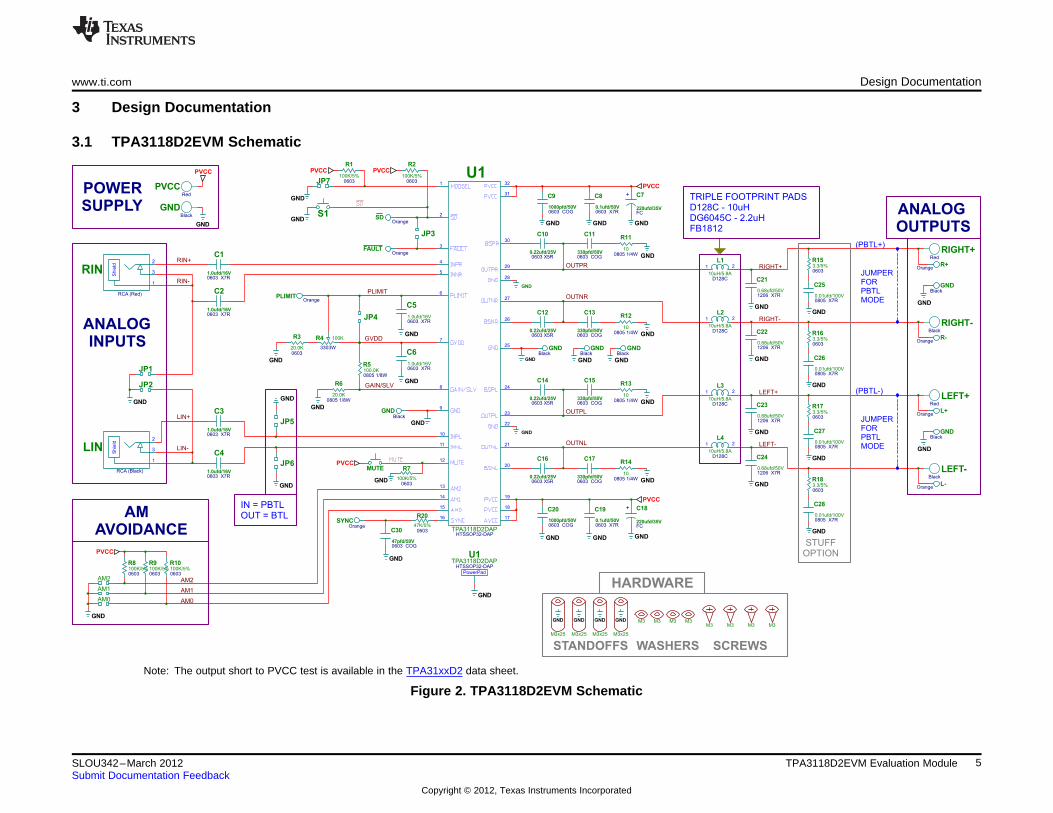
3.1 TPA3118D2EVM Schematic
Note: The output short to PVCC test is available in the TPA31xxD2 data sheet.
Figure 2. TPA3118D2EVM Schematic
5SLOU342–March 2012 TPA3118D2EVM Evaluation ModuleSubmit Documentation Feedback
Copyright © 2012, Texas Instruments Incorporated

Design Documentation www.ti.com
3.2 TPA3118D2EVM PCB Layers
Figure 3. TPA3118D2EVM Top Side Layout
Figure 4. TPA3118D2EVM Bottom Side Layout
6 TPA3118D2EVM Evaluation Module SLOU342–March 2012Submit Documentation Feedback
Copyright © 2012, Texas Instruments Incorporated

www.ti.com Design Documentation
Figure 5. TPA3118D2EVM Top X-ray View
7SLOU342–March 2012 TPA3118D2EVM Evaluation ModuleSubmit Documentation Feedback
Copyright © 2012, Texas Instruments Incorporated

Design Documentation www.ti.com
3.3 TPA3118D2EVM Bill of Materials
Table 2. TPA3118D2EVM Bill of Materials
Qty Ref Designators Description Manufacturer Part No. Manufacturer
1 U1 2 × 30 W CLASS D STEREO AMP HTSSOP32-DAP, RoHS TPA3118D2DAP TEXASINSTRUMENTS
1 C30 CAP SMD0603 CERM 47 pF, 50 V, 5%, COG, RoHS GRM1885C1H470JA01D MURATA
4 C11, C13, C15, C17 CAP SMD0603 CERM 330 pF, 50 V, 5%, COG, RoHS GRM1885C1H331JA01D MURATA
2 C9, C20 CAP SMD0603 CERM 1000 pF, 50 V, 5%, COG, RoHS C1608C0G1H102J TDK CORP.
4 C25, C26, C27, C28 CAP SMD0805 CERM 0.01 µF, 100 V, 10%, X7R, RoHS GRM21BR72A103KA01L MURATA
2 C8, C19 CAP SMD0603 CERM 0.1 µF, 50 V, 10%, X7R, RoHS GRM188R71H104KA93D MURATA
4 C10, C12, C14, C16 CAP SMD0603 CERM 0.22 µF, 25 V, 10%, X5R, RoHS 06033D224KAT2A AVX
4 C21, C22, C23, C24 CAP SMD1206 CERM 0.68 µF, 50 V, 10%, X7R, RoHS C1206C684K5RACTU KEMET
6 C1, C2, C3, C4, C5, CAP SMD0603 CERM 1.0 µF, 16 V, 10%, X7R, RoHS C1608X7R1C105K TDKC6
2 C7, C18 CAP THRU ALUM-ELECT FC SERIES 220 µF, 35 V, 20%, EEU-FC1V221L PANASONIC8 × 3.5 × 15 mm, RoHS
1 R20 RESISTOR SMD0603, 0 Ω, 1/10W, RoHS RMCF0603ZT0R00 STACKPOLEELECTRONICS
4 R15, R16, R17, R18 RESISTOR SMD0603, 3.3 Ω, 5%, 1/10W, RoHS ERJ-3GEYJ3R3V PANASONIC
4 R11, R12, R13, R14 RESISTOR SMD0805, 10 Ω, 1%, 1/4W, RoHS ESR10EZPJ100 ROHM
1 R3 RESISTOR SMD0603, THICK FILM, 1.00 kΩ, 1%, 1/10W, RoHS RC0603FR-071KL YAGEO
1 R21 RESISTOR SMD0603, 10.0 kΩ, 1%, THICK FILM, 1/10W, RoHS ERJ-3EKF1002V PANASONIC
1 R6 RESISTOR SMD0805, 20.0 kΩ, 1%, 1/8W, RoHS MCR10EZHF2002 ROHM
6 R1, R2, R7, R8, R9, RESISTOR SMD0603, 100 kΩ, 5%, 1/10W, RoHS RMCF0603JT100K STACKPOLER10 ELECTRONICS
1 R5 RESISTOR SMD0805, 100.0 kΩ, 1%, 1/8W, RoHS MCR10EZHF1003 ROHM
1 R4 POT SMD CERMET, 100 kΩ, 25%, SINGLE TURN TOP ADJ, 3303W-3-104E BOURNSRoHS
4 L1, L2, L3, L4 INDUCTOR, 10 µH, 5.8 A, TYPE D128C, RoHS 931BS-100M TOKO, INC.
10 AM0, AM1, AM2, JP1, HEADER THRU MALE 2 PIN 100LS, GOLD, RoHS PBC02SAAN SULLINSJP2, JP3, JP4, JP5,JP6, JP7
1 LIN JACK, RCA 3-PIN PCB-RA, BLACK, RoHS PJRAN1X1U01X SWITCHCRAFT
1 RIN JACK, RCA 3-PIN PCB-RA, RED, RoHS PJRAN1X1U013 SWITCHCRAFT
1 MASTER PC TESTPOINT, RED, RoHS 5000 KEYSTONEELECTRONICS
6 GND × 6 PC TESTPOINT, BLACK, RoHS 5001 KEYSTONEELECTRONICS
7 L+, L-, R+, R-, SD, PC TESTPOINT, ORANGE, RoHS 5003 KEYSTONEFAULT, PLIMIT ELECTRONICS
1 SLAVE PC TESTPOINT, YELLOW, RoHS 5004 KEYSTONEELECTRONICS
2 S1, MUTE SWITCH, MOM, 160 gf, SMT, 4 × 3 mm, RoHS TL1015AF160QG E-SWITCH
3 PVCC, LEFT+, BINDING POST, RED, 15 A, ECONO, RoHS 7006 KEYSTONERIGHT+ ELECTRONICS
3 GND, LEFT-, RIGHT- BINDING POST, BLACK, 15 A, ECONO, RoHS 7007 KEYSTONEELECTRONICS
7 AM0, AM1, AM2, JP1, SHUNT, BLACK AU FLASH 0.100LS SPC02SYAN SULLINSJP2, JP3, JP4, JP7
4 NA STANDOFF M3, 25 mm × 4.5 mm DIA HEX, 94868A178 MCMASTER-CARRSTAINLESS STEEL F-F, RoHS
4 NA WASHER SPLIT-LOCK M3, 6.2-mm OD, 0.7-mm THICK, 92148A150 MCMASTER-CARRSTAINLESS STEEL, RoHS
4 NA SCREW M3 × 8 PHILIPS PANHEAD STAINLESS STEEL, RoHS 92000A118 MCMASTER-CARR
8 TPA3118D2EVM Evaluation Module SLOU342–March 2012Submit Documentation Feedback
Copyright © 2012, Texas Instruments Incorporated

EVALUATION BOARD/KIT/MODULE (EVM) ADDITIONAL TERMS
Texas Instruments (TI) provides the enclosed Evaluation Board/Kit/Module (EVM) under the following conditions:
The user assumes all responsibility and liability for proper and safe handling of the goods. Further, the user indemnifies TI from all claimsarising from the handling or use of the goods.
Should this evaluation board/kit not meet the specifications indicated in the User’s Guide, the board/kit may be returned within 30 days fromthe date of delivery for a full refund. THE FOREGOING LIMITED WARRANTY IS THE EXCLUSIVE WARRANTY MADE BY SELLER TOBUYER AND IS IN LIEU OF ALL OTHER WARRANTIES, EXPRESSED, IMPLIED, OR STATUTORY, INCLUDING ANY WARRANTY OFMERCHANTABILITY OR FITNESS FOR ANY PARTICULAR PURPOSE. EXCEPT TO THE EXTENT OF THE INDEMNITY SET FORTHABOVE, NEITHER PARTY SHALL BE LIABLE TO THE OTHER FOR ANY INDIRECT, SPECIAL, INCIDENTAL, OR CONSEQUENTIALDAMAGES.
Please read the User's Guide and, specifically, the Warnings and Restrictions notice in the User's Guide prior to handling the product. Thisnotice contains important safety information about temperatures and voltages. For additional information on TI's environmental and/or safetyprograms, please visit www.ti.com/esh or contact TI.
No license is granted under any patent right or other intellectual property right of TI covering or relating to any machine, process, orcombination in which such TI products or services might be or are used. TI currently deals with a variety of customers for products, andtherefore our arrangement with the user is not exclusive. TI assumes no liability for applications assistance, customer product design,software performance, or infringement of patents or services described herein.
REGULATORY COMPLIANCE INFORMATION
As noted in the EVM User’s Guide and/or EVM itself, this EVM and/or accompanying hardware may or may not be subject to the FederalCommunications Commission (FCC) and Industry Canada (IC) rules.
For EVMs not subject to the above rules, this evaluation board/kit/module is intended for use for ENGINEERING DEVELOPMENT,DEMONSTRATION OR EVALUATION PURPOSES ONLY and is not considered by TI to be a finished end product fit for general consumeruse. It generates, uses, and can radiate radio frequency energy and has not been tested for compliance with the limits of computingdevices pursuant to part 15 of FCC or ICES-003 rules, which are designed to provide reasonable protection against radio frequencyinterference. Operation of the equipment may cause interference with radio communications, in which case the user at his own expense willbe required to take whatever measures may be required to correct this interference.
General Statement for EVMs including a radio
User Power/Frequency Use Obligations: This radio is intended for development/professional use only in legally allocated frequency andpower limits. Any use of radio frequencies and/or power availability of this EVM and its development application(s) must comply with locallaws governing radio spectrum allocation and power limits for this evaluation module. It is the user’s sole responsibility to only operate thisradio in legally acceptable frequency space and within legally mandated power limitations. Any exceptions to this are strictly prohibited andunauthorized by Texas Instruments unless user has obtained appropriate experimental/development licenses from local regulatoryauthorities, which is responsibility of user including its acceptable authorization.
For EVMs annotated as FCC – FEDERAL COMMUNICATIONS COMMISSION Part 15 Compliant
Caution
This device complies with part 15 of the FCC Rules. Operation is subject to the following two conditions: (1) This device may not causeharmful interference, and (2) this device must accept any interference received, including interference that may cause undesired operation.
Changes or modifications not expressly approved by the party responsible for compliance could void the user's authority to operate theequipment.
FCC Interference Statement for Class A EVM devices
This equipment has been tested and found to comply with the limits for a Class A digital device, pursuant to part 15 of the FCC Rules.These limits are designed to provide reasonable protection against harmful interference when the equipment is operated in a commercialenvironment. This equipment generates, uses, and can radiate radio frequency energy and, if not installed and used in accordance with theinstruction manual, may cause harmful interference to radio communications. Operation of this equipment in a residential area is likely tocause harmful interference in which case the user will be required to correct the interference at his own expense.

FCC Interference Statement for Class B EVM devices
This equipment has been tested and found to comply with the limits for a Class B digital device, pursuant to part 15 of the FCC Rules.These limits are designed to provide reasonable protection against harmful interference in a residential installation. This equipmentgenerates, uses and can radiate radio frequency energy and, if not installed and used in accordance with the instructions, may causeharmful interference to radio communications. However, there is no guarantee that interference will not occur in a particular installation. Ifthis equipment does cause harmful interference to radio or television reception, which can be determined by turning the equipment off andon, the user is encouraged to try to correct the interference by one or more of the following measures:
• Reorient or relocate the receiving antenna.• Increase the separation between the equipment and receiver.• Connect the equipment into an outlet on a circuit different from that to which the receiver is connected.• Consult the dealer or an experienced radio/TV technician for help.
For EVMs annotated as IC – INDUSTRY CANADA Compliant
This Class A or B digital apparatus complies with Canadian ICES-003.
Changes or modifications not expressly approved by the party responsible for compliance could void the user’s authority to operate theequipment.
Concerning EVMs including radio transmitters
This device complies with Industry Canada licence-exempt RSS standard(s). Operation is subject to the following two conditions: (1) thisdevice may not cause interference, and (2) this device must accept any interference, including interference that may cause undesiredoperation of the device.
Concerning EVMs including detachable antennas
Under Industry Canada regulations, this radio transmitter may only operate using an antenna of a type and maximum (or lesser) gainapproved for the transmitter by Industry Canada. To reduce potential radio interference to other users, the antenna type and its gain shouldbe so chosen that the equivalent isotropically radiated power (e.i.r.p.) is not more than that necessary for successful communication.
This radio transmitter has been approved by Industry Canada to operate with the antenna types listed in the user guide with the maximumpermissible gain and required antenna impedance for each antenna type indicated. Antenna types not included in this list, having a gaingreater than the maximum gain indicated for that type, are strictly prohibited for use with this device.
Cet appareil numérique de la classe A ou B est conforme à la norme NMB-003 du Canada.
Les changements ou les modifications pas expressément approuvés par la partie responsable de la conformité ont pu vider l’autorité del'utilisateur pour actionner l'équipement.
Concernant les EVMs avec appareils radio
Le présent appareil est conforme aux CNR d'Industrie Canada applicables aux appareils radio exempts de licence. L'exploitation estautorisée aux deux conditions suivantes : (1) l'appareil ne doit pas produire de brouillage, et (2) l'utilisateur de l'appareil doit accepter toutbrouillage radioélectrique subi, même si le brouillage est susceptible d'en compromettre le fonctionnement.
Concernant les EVMs avec antennes détachables
Conformément à la réglementation d'Industrie Canada, le présent émetteur radio peut fonctionner avec une antenne d'un type et d'un gainmaximal (ou inférieur) approuvé pour l'émetteur par Industrie Canada. Dans le but de réduire les risques de brouillage radioélectrique àl'intention des autres utilisateurs, il faut choisir le type d'antenne et son gain de sorte que la puissance isotrope rayonnée équivalente(p.i.r.e.) ne dépasse pas l'intensité nécessaire à l'établissement d'une communication satisfaisante.
Le présent émetteur radio a été approuvé par Industrie Canada pour fonctionner avec les types d'antenne énumérés dans le manueld’usage et ayant un gain admissible maximal et l'impédance requise pour chaque type d'antenne. Les types d'antenne non inclus danscette liste, ou dont le gain est supérieur au gain maximal indiqué, sont strictement interdits pour l'exploitation de l'émetteur.
SPACER
SPACER
SPACER
SPACER
SPACER
SPACER
SPACER
SPACER
【【Important Notice for Users of this Product in Japan】】This development kit is NOT certified as Confirming to Technical Regulations of Radio Law of Japan
If you use this product in Japan, you are required by Radio Law of Japan to follow the instructions below with respect to this product:
1. Use this product in a shielded room or any other test facility as defined in the notification #173 issued by Ministry of Internal Affairs andCommunications on March 28, 2006, based on Sub-section 1.1 of Article 6 of the Ministry’s Rule for Enforcement of Radio Law ofJapan,
2. Use this product only after you obtained the license of Test Radio Station as provided in Radio Law of Japan with respect to thisproduct, or
3. Use of this product only after you obtained the Technical Regulations Conformity Certification as provided in Radio Law of Japan withrespect to this product. Also, please do not transfer this product, unless you give the same notice above to the transferee. Please notethat if you could not follow the instructions above, you will be subject to penalties of Radio Law of Japan.
Texas Instruments Japan Limited(address) 24-1, Nishi-Shinjuku 6 chome, Shinjuku-ku, Tokyo, Japan
http://www.tij.co.jp
【ご使用にあたっての注】
本開発キットは技術基準適合証明を受けておりません。
本製品のご使用に際しては、電波法遵守のため、以下のいずれかの措置を取っていただく必要がありますのでご注意ください。1. 電波法施行規則第6条第1項第1号に基づく平成18年3月28日総務省告示第173号で定められた電波暗室等の試験設備でご使用いただく。2. 実験局の免許を取得後ご使用いただく。3. 技術基準適合証明を取得後ご使用いただく。
なお、本製品は、上記の「ご使用にあたっての注意」を譲渡先、移転先に通知しない限り、譲渡、移転できないものとします。
上記を遵守頂けない場合は、電波法の罰則が適用される可能性があることをご留意ください。
日本テキサス・インスツルメンツ株式会社東京都新宿区西新宿6丁目24番1号西新宿三井ビルhttp://www.tij.co.jp
SPACER
SPACER
SPACER
SPACER
SPACER
SPACER
SPACER
SPACER
SPACER
SPACER
SPACER
SPACER
SPACER
SPACER
SPACER
SPACER

EVALUATION BOARD/KIT/MODULE (EVM)WARNINGS, RESTRICTIONS AND DISCLAIMERS
For Feasibility Evaluation Only, in Laboratory/Development Environments. Unless otherwise indicated, this EVM is not a finishedelectrical equipment and not intended for consumer use. It is intended solely for use for preliminary feasibility evaluation inlaboratory/development environments by technically qualified electronics experts who are familiar with the dangers and application risksassociated with handling electrical mechanical components, systems and subsystems. It should not be used as all or part of a finished endproduct.
Your Sole Responsibility and Risk. You acknowledge, represent and agree that:
1. You have unique knowledge concerning Federal, State and local regulatory requirements (including but not limited to Food and DrugAdministration regulations, if applicable) which relate to your products and which relate to your use (and/or that of your employees,affiliates, contractors or designees) of the EVM for evaluation, testing and other purposes.
2. You have full and exclusive responsibility to assure the safety and compliance of your products with all such laws and other applicableregulatory requirements, and also to assure the safety of any activities to be conducted by you and/or your employees, affiliates,contractors or designees, using the EVM. Further, you are responsible to assure that any interfaces (electronic and/or mechanical)between the EVM and any human body are designed with suitable isolation and means to safely limit accessible leakage currents tominimize the risk of electrical shock hazard.
3. You will employ reasonable safeguards to ensure that your use of the EVM will not result in any property damage, injury or death, evenif the EVM should fail to perform as described or expected.
4. You will take care of proper disposal and recycling of the EVM’s electronic components and packing materials.
Certain Instructions. It is important to operate this EVM within TI’s recommended specifications and environmental considerations per theuser guidelines. Exceeding the specified EVM ratings (including but not limited to input and output voltage, current, power, andenvironmental ranges) may cause property damage, personal injury or death. If there are questions concerning these ratings please contacta TI field representative prior to connecting interface electronics including input power and intended loads. Any loads applied outside of thespecified output range may result in unintended and/or inaccurate operation and/or possible permanent damage to the EVM and/orinterface electronics. Please consult the EVM User's Guide prior to connecting any load to the EVM output. If there is uncertainty as to theload specification, please contact a TI field representative. During normal operation, some circuit components may have case temperaturesgreater than 60°C as long as the input and output are maintained at a normal ambient operating temperature. These components includebut are not limited to linear regulators, switching transistors, pass transistors, and current sense resistors which can be identified using theEVM schematic located in the EVM User's Guide. When placing measurement probes near these devices during normal operation, pleasebe aware that these devices may be very warm to the touch. As with all electronic evaluation tools, only qualified personnel knowledgeablein electronic measurement and diagnostics normally found in development environments should use these EVMs.
Agreement to Defend, Indemnify and Hold Harmless. You agree to defend, indemnify and hold TI, its licensors and their representativesharmless from and against any and all claims, damages, losses, expenses, costs and liabilities (collectively, "Claims") arising out of or inconnection with any use of the EVM that is not in accordance with the terms of the agreement. This obligation shall apply whether Claimsarise under law of tort or contract or any other legal theory, and even if the EVM fails to perform as described or expected.
Safety-Critical or Life-Critical Applications. If you intend to evaluate the components for possible use in safety critical applications (suchas life support) where a failure of the TI product would reasonably be expected to cause severe personal injury or death, such as deviceswhich are classified as FDA Class III or similar classification, then you must specifically notify TI of such intent and enter into a separateAssurance and Indemnity Agreement.
Mailing Address: Texas Instruments, Post Office Box 655303, Dallas, Texas 75265Copyright © 2012, Texas Instruments Incorporated

EVALUATION BOARD/KIT/MODULE (EVM) ADDITIONAL TERMSTexas Instruments (TI) provides the enclosed Evaluation Board/Kit/Module (EVM) under the following conditions:
The user assumes all responsibility and liability for proper and safe handling of the goods. Further, the user indemnifies TI from all claimsarising from the handling or use of the goods.
Should this evaluation board/kit not meet the specifications indicated in the User’s Guide, the board/kit may be returned within 30 days fromthe date of delivery for a full refund. THE FOREGOING LIMITED WARRANTY IS THE EXCLUSIVE WARRANTY MADE BY SELLER TOBUYER AND IS IN LIEU OF ALL OTHER WARRANTIES, EXPRESSED, IMPLIED, OR STATUTORY, INCLUDING ANY WARRANTY OFMERCHANTABILITY OR FITNESS FOR ANY PARTICULAR PURPOSE. EXCEPT TO THE EXTENT OF THE INDEMNITY SET FORTHABOVE, NEITHER PARTY SHALL BE LIABLE TO THE OTHER FOR ANY INDIRECT, SPECIAL, INCIDENTAL, OR CONSEQUENTIALDAMAGES.
Please read the User's Guide and, specifically, the Warnings and Restrictions notice in the User's Guide prior to handling the product. Thisnotice contains important safety information about temperatures and voltages. For additional information on TI's environmental and/or safetyprograms, please visit www.ti.com/esh or contact TI.
No license is granted under any patent right or other intellectual property right of TI covering or relating to any machine, process, orcombination in which such TI products or services might be or are used. TI currently deals with a variety of customers for products, andtherefore our arrangement with the user is not exclusive. TI assumes no liability for applications assistance, customer product design,software performance, or infringement of patents or services described herein.
REGULATORY COMPLIANCE INFORMATIONAs noted in the EVM User’s Guide and/or EVM itself, this EVM and/or accompanying hardware may or may not be subject to the FederalCommunications Commission (FCC) and Industry Canada (IC) rules.
For EVMs not subject to the above rules, this evaluation board/kit/module is intended for use for ENGINEERING DEVELOPMENT,DEMONSTRATION OR EVALUATION PURPOSES ONLY and is not considered by TI to be a finished end product fit for general consumeruse. It generates, uses, and can radiate radio frequency energy and has not been tested for compliance with the limits of computingdevices pursuant to part 15 of FCC or ICES-003 rules, which are designed to provide reasonable protection against radio frequencyinterference. Operation of the equipment may cause interference with radio communications, in which case the user at his own expense willbe required to take whatever measures may be required to correct this interference.
General Statement for EVMs including a radioUser Power/Frequency Use Obligations: This radio is intended for development/professional use only in legally allocated frequency andpower limits. Any use of radio frequencies and/or power availability of this EVM and its development application(s) must comply with locallaws governing radio spectrum allocation and power limits for this evaluation module. It is the user’s sole responsibility to only operate thisradio in legally acceptable frequency space and within legally mandated power limitations. Any exceptions to this are strictly prohibited andunauthorized by Texas Instruments unless user has obtained appropriate experimental/development licenses from local regulatoryauthorities, which is responsibility of user including its acceptable authorization.
For EVMs annotated as FCC – FEDERAL COMMUNICATIONS COMMISSION Part 15 Compliant
CautionThis device complies with part 15 of the FCC Rules. Operation is subject to the following two conditions: (1) This device may not causeharmful interference, and (2) this device must accept any interference received, including interference that may cause undesired operation.
Changes or modifications not expressly approved by the party responsible for compliance could void the user's authority to operate theequipment.
FCC Interference Statement for Class A EVM devicesThis equipment has been tested and found to comply with the limits for a Class A digital device, pursuant to part 15 of the FCC Rules.These limits are designed to provide reasonable protection against harmful interference when the equipment is operated in a commercialenvironment. This equipment generates, uses, and can radiate radio frequency energy and, if not installed and used in accordance with theinstruction manual, may cause harmful interference to radio communications. Operation of this equipment in a residential area is likely tocause harmful interference in which case the user will be required to correct the interference at his own expense.

FCC Interference Statement for Class B EVM devicesThis equipment has been tested and found to comply with the limits for a Class B digital device, pursuant to part 15 of the FCC Rules.These limits are designed to provide reasonable protection against harmful interference in a residential installation. This equipmentgenerates, uses and can radiate radio frequency energy and, if not installed and used in accordance with the instructions, may causeharmful interference to radio communications. However, there is no guarantee that interference will not occur in a particular installation. Ifthis equipment does cause harmful interference to radio or television reception, which can be determined by turning the equipment off andon, the user is encouraged to try to correct the interference by one or more of the following measures:
• Reorient or relocate the receiving antenna.• Increase the separation between the equipment and receiver.• Connect the equipment into an outlet on a circuit different from that to which the receiver is connected.• Consult the dealer or an experienced radio/TV technician for help.
For EVMs annotated as IC – INDUSTRY CANADA Compliant
This Class A or B digital apparatus complies with Canadian ICES-003.
Changes or modifications not expressly approved by the party responsible for compliance could void the user’s authority to operate theequipment.
Concerning EVMs including radio transmitters
This device complies with Industry Canada licence-exempt RSS standard(s). Operation is subject to the following two conditions: (1) thisdevice may not cause interference, and (2) this device must accept any interference, including interference that may cause undesiredoperation of the device.
Concerning EVMs including detachable antennasUnder Industry Canada regulations, this radio transmitter may only operate using an antenna of a type and maximum (or lesser) gainapproved for the transmitter by Industry Canada. To reduce potential radio interference to other users, the antenna type and its gain shouldbe so chosen that the equivalent isotropically radiated power (e.i.r.p.) is not more than that necessary for successful communication.
This radio transmitter has been approved by Industry Canada to operate with the antenna types listed in the user guide with the maximumpermissible gain and required antenna impedance for each antenna type indicated. Antenna types not included in this list, having a gaingreater than the maximum gain indicated for that type, are strictly prohibited for use with this device.
Cet appareil numérique de la classe A ou B est conforme à la norme NMB-003 du Canada.
Les changements ou les modifications pas expressément approuvés par la partie responsable de la conformité ont pu vider l’autorité del'utilisateur pour actionner l'équipement.
Concernant les EVMs avec appareils radio
Le présent appareil est conforme aux CNR d'Industrie Canada applicables aux appareils radio exempts de licence. L'exploitation estautorisée aux deux conditions suivantes : (1) l'appareil ne doit pas produire de brouillage, et (2) l'utilisateur de l'appareil doit accepter toutbrouillage radioélectrique subi, même si le brouillage est susceptible d'en compromettre le fonctionnement.
Concernant les EVMs avec antennes détachables
Conformément à la réglementation d'Industrie Canada, le présent émetteur radio peut fonctionner avec une antenne d'un type et d'un gainmaximal (ou inférieur) approuvé pour l'émetteur par Industrie Canada. Dans le but de réduire les risques de brouillage radioélectrique àl'intention des autres utilisateurs, il faut choisir le type d'antenne et son gain de sorte que la puissance isotrope rayonnée équivalente(p.i.r.e.) ne dépasse pas l'intensité nécessaire à l'établissement d'une communication satisfaisante.
Le présent émetteur radio a été approuvé par Industrie Canada pour fonctionner avec les types d'antenne énumérés dans le manueld’usage et ayant un gain admissible maximal et l'impédance requise pour chaque type d'antenne. Les types d'antenne non inclus danscette liste, ou dont le gain est supérieur au gain maximal indiqué, sont strictement interdits pour l'exploitation de l'émetteur.
SPACER
SPACER
SPACER
SPACER
SPACER
SPACER
SPACER
SPACER

【【Important Notice for Users of this Product in Japan】】This development kit is NOT certified as Confirming to Technical Regulations of Radio Law of Japan
If you use this product in Japan, you are required by Radio Law of Japan to follow the instructions below with respect to this product:
1. Use this product in a shielded room or any other test facility as defined in the notification #173 issued by Ministry of Internal Affairs andCommunications on March 28, 2006, based on Sub-section 1.1 of Article 6 of the Ministry’s Rule for Enforcement of Radio Law ofJapan,
2. Use this product only after you obtained the license of Test Radio Station as provided in Radio Law of Japan with respect to thisproduct, or
3. Use of this product only after you obtained the Technical Regulations Conformity Certification as provided in Radio Law of Japan withrespect to this product. Also, please do not transfer this product, unless you give the same notice above to the transferee. Please notethat if you could not follow the instructions above, you will be subject to penalties of Radio Law of Japan.
Texas Instruments Japan Limited(address) 24-1, Nishi-Shinjuku 6 chome, Shinjuku-ku, Tokyo, Japan
http://www.tij.co.jp
【ご使用にあたっての注】
本開発キットは技術基準適合証明を受けておりません。
本製品のご使用に際しては、電波法遵守のため、以下のいずれかの措置を取っていただく必要がありますのでご注意ください。1. 電波法施行規則第6条第1項第1号に基づく平成18年3月28日総務省告示第173号で定められた電波暗室等の試験設備でご使用いただく。2. 実験局の免許を取得後ご使用いただく。3. 技術基準適合証明を取得後ご使用いただく。
なお、本製品は、上記の「ご使用にあたっての注意」を譲渡先、移転先に通知しない限り、譲渡、移転できないものとします。
上記を遵守頂けない場合は、電波法の罰則が適用される可能性があることをご留意ください。
日本テキサス・インスツルメンツ株式会社東京都新宿区西新宿6丁目24番1号西新宿三井ビルhttp://www.tij.co.jp
SPACER
SPACER
SPACER
SPACER
SPACER
SPACER
SPACER
SPACER
SPACER
SPACER
SPACER
SPACER
SPACER
SPACER
SPACER
SPACER

EVALUATION BOARD/KIT/MODULE (EVM)WARNINGS, RESTRICTIONS AND DISCLAIMERS
For Feasibility Evaluation Only, in Laboratory/Development Environments. Unless otherwise indicated, this EVM is not a finishedelectrical equipment and not intended for consumer use. It is intended solely for use for preliminary feasibility evaluation inlaboratory/development environments by technically qualified electronics experts who are familiar with the dangers and application risksassociated with handling electrical mechanical components, systems and subsystems. It should not be used as all or part of a finished endproduct.
Your Sole Responsibility and Risk. You acknowledge, represent and agree that:
1. You have unique knowledge concerning Federal, State and local regulatory requirements (including but not limited to Food and DrugAdministration regulations, if applicable) which relate to your products and which relate to your use (and/or that of your employees,affiliates, contractors or designees) of the EVM for evaluation, testing and other purposes.
2. You have full and exclusive responsibility to assure the safety and compliance of your products with all such laws and other applicableregulatory requirements, and also to assure the safety of any activities to be conducted by you and/or your employees, affiliates,contractors or designees, using the EVM. Further, you are responsible to assure that any interfaces (electronic and/or mechanical)between the EVM and any human body are designed with suitable isolation and means to safely limit accessible leakage currents tominimize the risk of electrical shock hazard.
3. You will employ reasonable safeguards to ensure that your use of the EVM will not result in any property damage, injury or death, evenif the EVM should fail to perform as described or expected.
4. You will take care of proper disposal and recycling of the EVM’s electronic components and packing materials.
Certain Instructions. It is important to operate this EVM within TI’s recommended specifications and environmental considerations per theuser guidelines. Exceeding the specified EVM ratings (including but not limited to input and output voltage, current, power, andenvironmental ranges) may cause property damage, personal injury or death. If there are questions concerning these ratings please contacta TI field representative prior to connecting interface electronics including input power and intended loads. Any loads applied outside of thespecified output range may result in unintended and/or inaccurate operation and/or possible permanent damage to the EVM and/orinterface electronics. Please consult the EVM User's Guide prior to connecting any load to the EVM output. If there is uncertainty as to theload specification, please contact a TI field representative. During normal operation, some circuit components may have case temperaturesgreater than 60°C as long as the input and output are maintained at a normal ambient operating temperature. These components includebut are not limited to linear regulators, switching transistors, pass transistors, and current sense resistors which can be identified using theEVM schematic located in the EVM User's Guide. When placing measurement probes near these devices during normal operation, pleasebe aware that these devices may be very warm to the touch. As with all electronic evaluation tools, only qualified personnel knowledgeablein electronic measurement and diagnostics normally found in development environments should use these EVMs.
Agreement to Defend, Indemnify and Hold Harmless. You agree to defend, indemnify and hold TI, its licensors and their representativesharmless from and against any and all claims, damages, losses, expenses, costs and liabilities (collectively, "Claims") arising out of or inconnection with any use of the EVM that is not in accordance with the terms of the agreement. This obligation shall apply whether Claimsarise under law of tort or contract or any other legal theory, and even if the EVM fails to perform as described or expected.
Safety-Critical or Life-Critical Applications. If you intend to evaluate the components for possible use in safety critical applications (suchas life support) where a failure of the TI product would reasonably be expected to cause severe personal injury or death, such as deviceswhich are classified as FDA Class III or similar classification, then you must specifically notify TI of such intent and enter into a separateAssurance and Indemnity Agreement.
Mailing Address: Texas Instruments, Post Office Box 655303, Dallas, Texas 75265Copyright © 2012, Texas Instruments Incorporated

IMPORTANT NOTICE
Texas Instruments Incorporated and its subsidiaries (TI) reserve the right to make corrections, enhancements, improvements and otherchanges to its semiconductor products and services per JESD46, latest issue, and to discontinue any product or service per JESD48, latestissue. Buyers should obtain the latest relevant information before placing orders and should verify that such information is current andcomplete. All semiconductor products (also referred to herein as “components”) are sold subject to TI’s terms and conditions of salesupplied at the time of order acknowledgment.
TI warrants performance of its components to the specifications applicable at the time of sale, in accordance with the warranty in TI’s termsand conditions of sale of semiconductor products. Testing and other quality control techniques are used to the extent TI deems necessaryto support this warranty. Except where mandated by applicable law, testing of all parameters of each component is not necessarilyperformed.
TI assumes no liability for applications assistance or the design of Buyers’ products. Buyers are responsible for their products andapplications using TI components. To minimize the risks associated with Buyers’ products and applications, Buyers should provideadequate design and operating safeguards.
TI does not warrant or represent that any license, either express or implied, is granted under any patent right, copyright, mask work right, orother intellectual property right relating to any combination, machine, or process in which TI components or services are used. Informationpublished by TI regarding third-party products or services does not constitute a license to use such products or services or a warranty orendorsement thereof. Use of such information may require a license from a third party under the patents or other intellectual property of thethird party, or a license from TI under the patents or other intellectual property of TI.
Reproduction of significant portions of TI information in TI data books or data sheets is permissible only if reproduction is without alterationand is accompanied by all associated warranties, conditions, limitations, and notices. TI is not responsible or liable for such altereddocumentation. Information of third parties may be subject to additional restrictions.
Resale of TI components or services with statements different from or beyond the parameters stated by TI for that component or servicevoids all express and any implied warranties for the associated TI component or service and is an unfair and deceptive business practice.TI is not responsible or liable for any such statements.
Buyer acknowledges and agrees that it is solely responsible for compliance with all legal, regulatory and safety-related requirementsconcerning its products, and any use of TI components in its applications, notwithstanding any applications-related information or supportthat may be provided by TI. Buyer represents and agrees that it has all the necessary expertise to create and implement safeguards whichanticipate dangerous consequences of failures, monitor failures and their consequences, lessen the likelihood of failures that might causeharm and take appropriate remedial actions. Buyer will fully indemnify TI and its representatives against any damages arising out of the useof any TI components in safety-critical applications.
In some cases, TI components may be promoted specifically to facilitate safety-related applications. With such components, TI’s goal is tohelp enable customers to design and create their own end-product solutions that meet applicable functional safety standards andrequirements. Nonetheless, such components are subject to these terms.
No TI components are authorized for use in FDA Class III (or similar life-critical medical equipment) unless authorized officers of the partieshave executed a special agreement specifically governing such use.
Only those TI components which TI has specifically designated as military grade or “enhanced plastic” are designed and intended for use inmilitary/aerospace applications or environments. Buyer acknowledges and agrees that any military or aerospace use of TI componentswhich have not been so designated is solely at the Buyer's risk, and that Buyer is solely responsible for compliance with all legal andregulatory requirements in connection with such use.
TI has specifically designated certain components which meet ISO/TS16949 requirements, mainly for automotive use. Components whichhave not been so designated are neither designed nor intended for automotive use; and TI will not be responsible for any failure of suchcomponents to meet such requirements.
Products Applications
Audio www.ti.com/audio Automotive and Transportation www.ti.com/automotive
Amplifiers amplifier.ti.com Communications and Telecom www.ti.com/communications
Data Converters dataconverter.ti.com Computers and Peripherals www.ti.com/computers
DLP® Products www.dlp.com Consumer Electronics www.ti.com/consumer-apps
DSP dsp.ti.com Energy and Lighting www.ti.com/energy
Clocks and Timers www.ti.com/clocks Industrial www.ti.com/industrial
Interface interface.ti.com Medical www.ti.com/medical
Logic logic.ti.com Security www.ti.com/security
Power Mgmt power.ti.com Space, Avionics and Defense www.ti.com/space-avionics-defense
Microcontrollers microcontroller.ti.com Video and Imaging www.ti.com/video
RFID www.ti-rfid.com
OMAP Applications Processors www.ti.com/omap TI E2E Community e2e.ti.com
Wireless Connectivity www.ti.com/wirelessconnectivity
Mailing Address: Texas Instruments, Post Office Box 655303, Dallas, Texas 75265Copyright © 2012, Texas Instruments Incorporated