TP2808 - ECA
23
TP2808 8051 MICROCONTROLLER WITH 128K FLASH AND ISP Data Sheet-Version 0.92 Page 1 of 23 http://www.topro.com.tw June 2004 General Description The Topro TP2808 is an 8-bit microcontroller, which has an in-system programmable FLASH EPROM for firmware updating and fully compatible instruction set with the standard 8051. It contains a 128K-byte FLASH EPROM, 1K bytes of on-chip RAM, four 8-bit bi-directional and bit-addressable I/O ports, an additional 4-bit port P4, three 16-bit timer/counters, a serial port, 7-channel PWM and 4-channel 6-bit ADC, and is available in 44-pin PLCC, 44-pin QFP, 40-pin DIP package forms. Applications LCD TV LCD Monitor Flat Panel Display Features Fully static design of 8-bit CMOS microcontroller up to 40 MH Z 128K-byte FLASH EPROM Low standby current at full supply voltage 1K bytes of on-chip RAM (including 768 bytes of AUX-RAM, software selectable) Four 8-bit bi-directional ports One 4-bit multipurpose programmable port Three 16-bit timer/counters One full duplex serial port 7-channel PWM DAC 4-channel 6-bit ADC Built-in power management for low stand-by consumption Code protection Compliant with VESA DDC1/DDC2B/DDC2Bi Package Forms: 44-pin PLCC, 44-pin QFP, 40-pin DIP Ordering Information TP2808 Block Diagram Voltage Voltage L: 3.3V H: 5V Package Type P: DIP C: PLCC Q: PQFP Package Type
Transcript of TP2808 - ECA

TP28088051 MICROCONTROLLER WITH 128K FLASH AND ISP
Data Sheet-Version 0.92 Page 1 of 23 http://www.topro.com.tw June 2004
General Description
The Topro TP2808 is an 8-bit microcontroller, which has an in-system programmable FLASH EPROM for firmware updating and fully compatible instruction set with the standard 8051. It contains a 128K-byte FLASH EPROM, 1K bytes of on-chip RAM, four 8-bit bi-directional and bit-addressable I/O ports, an additional 4-bit port P4, three 16-bit timer/counters, a serial port, 7-channel PWM and 4-channel 6-bit ADC, and is available in 44-pin PLCC, 44-pin QFP, 40-pin DIP package forms.
Applications
LCD TV LCD Monitor Flat Panel Display
Features
Fully static design of 8-bit CMOS microcontroller up to 40 MHZ
128K-byte FLASH EPROM Low standby current at full supply voltage 1K bytes of on-chip RAM (including 768 bytes of
AUX-RAM, software selectable) Four 8-bit bi-directional ports One 4-bit multipurpose programmable port Three 16-bit timer/counters One full duplex serial port 7-channel PWM DAC 4-channel 6-bit ADC Built-in power management for low stand-by
consumption Code protection Compliant with VESA DDC1/DDC2B/DDC2Bi Package Forms: 44-pin PLCC, 44-pin QFP,
40-pin DIP Ordering Information
TP2808
Block Diagram
Voltage
Voltage L: 3.3V H: 5V
Package Type P: DIP C: PLCC Q: PQFP
Package Type

TP28088051 MICROCONTROLLER WITH 128K FLASH AND ISP
Data Sheet-Version 0.92 Page 2 of 23 http://www.topro.com.tw June 2004
Pin Configurations 44-pin PLCC
44-pin PQFP
40-pin DIP
1
2
3
4
5
6
7
8
9
10
11
33
32
31
30
29
28
27
26
25
24
23
12 13 14 15 16 17 18 19 20 21 22
44 43 42 41 40 39 38 37 36 35 34
WR,
P3.6
RD,P
3.7
XTAL
2XT
AL1
VSS
P4.0
,AD
0P2
.0,H
YNSC
P2.1
,VSY
NC
P2.2
,SCL
P2.3
,SD
AP2
.4
P0.4
P0.5
P0.6
P0.7
EA
P4.1,AD1
ALE
PSEN
P2.7
P2.6
P2.5
P1.5
P1.6/PWM2.1
P1.7/PWM2.0
RST
RXD,P3.0
INT2,P4.3,AD3
TXD,P3.1
INT0,P3.2
INT1,P3.3
T0,P3.4
T1,P3.5
P1.4
,PW
M4
P1.3
,PW
M3
P1.2
,PW
M2
P1.1
,PM
W1
P1.0
,PW
M0
P4.2
,INT,
AD
3VD
DP0
.0P0
.1P0
.2P0
.3

TP28088051 MICROCONTROLLER WITH 128K FLASH AND ISP
Data Sheet-Version 0.92 Page 3 of 23 http://www.topro.com.tw June 2004
Pin Descriptions
Symbol Type Description
EA I
EXTERIAL ACCESS ENABLE This pin forces the processor to execute the external ROM. The ROM address and data
will not be presented on the bus if the EA pin is high and the program counter is within the 64KB area.
PSEN O H
PROGRAM STORE ENABLE
PSEN enables the external ROM data in the Port 0 address/data bus. When internal
ROM access is performed, no PSEN strobe signal outputs originate from this pin.
ALE O H
ADDRESSLATCH ENABLE ALE is used to enable the address latch that separates the address from the data on Port 0. ALE runs at 1/6th of the oscillator frequency. An ALE pulse is omitted during external data memory accesses.
RST I L RESET A high on this pin for two machine cycles while the oscillator is running resets the device.
XTAL1 I CRYSTAL 1: This is the crystal oscillator input pin and may be driven by an external clock. XTAL2 O CRYSTAL 2: This is the crystal oscillator output pin and is the inversion of XTAL1.
VSS I GROUND: ground potential VDD I POWER SUPPLY: Supply voltage for operation
P0.0 - P0.7 I/O D PORT 0: Function is the same as that of standard 8051. P1.0/PWM0 I/O General purpose I/O (8051 standard) / PWMDAC0 output (CMOS) P1.1/PWM1 I/O General purpose I/O (8051 standard) / PWMDAC1 output (CMOS) P1.2/PWM2 I/O General purpose I/O (8051 standard) / PWMDAC2 output (CMOS) P1.3/PWM3 I/O General purpose I/O (8051 standard) / PWMDAC3 output (CMOS) P1.4/PWM4 I/O General purpose I/O (8051 standard) / PWMDAC4 output (CMOS)
P1.5 I/O General purpose I/O (8051 standard) P.1.6/PWM2.1 I/O General purpose I/O (8051 standard) / PWM2.1DAC output (CMOS) P1.7/PWM2.0 I/O General purpose I/O (8051 standard) / PWM2.0DAC output (CMOS)
P2.0 - P2.7 I/O
PORT 2: Port 2 is a bi-directional I/O port with internal pull-ups. This port also provides the upper address bits for accesses to external memory.
P2.0 is also used for HSYNC input. P2.1 is also used for VSYNC input. P2.2 is also used for SCL P2.3 is also used for SDA
P3.0 - P3.7 I/O PORT 3: Function is the same as that of the standard 8051. P3.5 is used to select the bank of 128K flash ROM
P4.0/AD0 I/O General purpose I/O (8051 standard) / ADC input P4.1/AD1 I/O General purpose I/O (8051 standard) / ADC input
P4.2/INT2/AD2 I/O General purpose I/O (8051 standard) / external interrupt input / ADC input P4.3/INT3/AD3 I/O General purpose I/O (8051 standard) / external interrupt input / ADC input

TP28088051 MICROCONTROLLER WITH 128K FLASH AND ISP
Data Sheet-Version 0.92 Page 4 of 23 http://www.topro.com.tw June 2004
Functional Description The TP2808 architecture consists of a core controller surrounded by various registers, four general-purpose I/O ports, 1K bytes of RAM, three timer/counters, and a serial port. The processor supports 111 different opcodes and references both with a 64K program address space and a 64K data storage space.
RAM
The internal data RAM in the TP2808 is 1032 bytes and is divided into two banks: 256 bytes of scratchpad RAM and 768 bytes of AUX-RAM, both addressed by different ways.
1. RAM 0H-7HF It can be addressed directly and indirectly as the same as in 8051. Address pointers are R0 and R1 of the selected register bank.
2. RAM 80H-FFH It can only be addressed indirectly as the same as in 8051. Address pointers are R0 and R1 of the selected registers bank.
3. AUX-RAM 0H-302H It is addressed indirectly as the same way to access external data memory with the MOVX instruction. Address pointers are R0 of the selected register bank and DPTR register. An access to external data memory locations higher than FFH will be performed with the MOVX instruction in the same way as in the 8051. The AUX-RAM is disabled after a reset. Setting the bit 4 in CHPCON register will enable the access to on-chip AUX-RAM. When executing from internal program memory, an access to AUX-RAM will not affect the ports P0, P2, WR and RD .
Timers 0,1 and 2
Timers 0, 1, and 2 each consist of two 8-bit data registers. These are called TL0 and TH0 for Timer 0, TL1 and TH1 for Timer 1, and TL2 and TH2 for Timer 2. The TCON and TMOD registers provide control functions for Timers 0, 1. The T2CON register provides control functions for Timer 2. RCAP2H and RCAP2L are used as reload/capture registers for Timer 2.
The operations of Timer 0 and Timer 1 are the same as in the W78C51. Timer 2 is a 16-bit timer/counter that is configured and controlled by the T2CON register. Like Timers 0 and 1, Timer 2 can operate either as an external event counter or as an internal timer, depending on the setting of bit C/T2 in T2CON. Timer 2 has three operating modes: Capture, Auto-reload, and Baud Rate Generator. The clock speed at Capture or Auto-reload mode is the same as that of Timers 0 and 1.
2INT / 3INT Two additional external interrupts, 2INT and
3INT , whose functions are similar to those of external interrupt 0 and 1 in the XICON (External Interrupt Control) register. The XICON register is bit-addressable but is not a standard register in the standard 8051. Its address is at 0C0H. To set/clear bits in the XICON register, one can use the “SETB ( 3INT ) bit” instruction. For example, “SETB 0C2H” sets the EX2 bit of XICON.
XICON-External Interrupt Control (C0H)
PX3 EX3 IE3 IT3 PX2 EX2 IE2 IT2
PX3: External interrupt 3 priority high if set. EX3: External interrupt 3 enable if set. IE3: If IT3 = 1, IE3 is set/cleared automatically by
hardware when interrupt is detected/serviced. IT3: External interrupt 3 is falling-edge/low-level
triggered when this bit is set/cleared by software.
PX2: External interrupt 2 priority high if set. EX2: External interrupt 2 enable if set. IE2: If IT2 = 1, IE2 is set/cleared automatically by
hardware when interrupt is detected/serviced. IT2: External interrupt 2 is falling-edge/low-level
triggered when this bit is set/cleared by software.
TP28088051 MICROCONTROLLER WITH 128K FLASH AND ISP
Data Sheet-Version 0.92 Page 5 of 23 http://www.topro.com.tw June 2004
9-source Interrupt Information
Interrupt Source Vector Address
Polling Sequence Within Priority Level
Enable RequiredSettings
Interrupt Type Edge/Level
External Interrupt 0 03H 0 (highest) IE.0 TCON.0 Timer/Counter 0 0BH 1 IE.1 - External Interrupt 1 13H 2 IE.2 TCON.2 Timer/Counter 1 1BH 3 IE.3 - External Interrupt 2 23H 4 IE.4 - Timer/Counter 2 2BH 5 IE.5 - External Interrupt 3 33H 6 XICON.2 XICON.0 Timer/Counter 3 3BH 7 XICON.6 XICON.3 DDC2 43h 8 (Lowest) See DDC IP
Pad Function Control Please refer to the part of Pin Configurations for the each function. Reg. Name Addr. Bit7 Bit6 Bit5 Bit4 Bit3 Bit2 Bit1 Bit0 PADOPT 0f50h(w) - - - - AD3E AD2E AD1E AD0E PADOPT 0f51h(w) PWMf PWMd - PWM4 PWM3 PWM2 PWM1 PWM0
PADOPT (w): control registers in a pad mode, all-standing for “0” in chip Reset.
AD3E = 1 -> Pin “P4.3/AD3” for AD3 = 0 -> Pin “P4.3/AD3” for P4.3 AD2E = 1 -> Pin “P4.2/AD2” for AD2 = 0 -> Pin “P4.2/AD2” for P4.2 AD1E = 1 -> Pin “P4.1/AD1” for AD1 = 0 -> Pin “P4.1/AD1” for P4.1 AD0E = 1 -> Pin “P4.0/AD0” for AD0 = 0 -> Pin “P4.0/AD0” for P4.0 PWMf = 1 -> Selection of 94KHz PWM frequency = 0 -> Selection of 47KHz PWM frequency PWMd = 1 -> PWM pulse width for 253-step
resolution = 0 -> PWM pulse width for 256-step
resolution PWM4 = 1 -> Pin “P1.4/PWM4” for PWM4 = 0 -> Pin “P1.4/PWM4” for P1.4 PWM3 = 1 -> Pin “P1.3/PWM3” for PWM3 = 0 -> Pin “P1.3/PWM3” for P1.3 PWM2 = 1 -> Pin “P1.2/PWM2” for PWM2 = 0 -> Pin “P1.2/PWM2” for P1.2 PWM1 = 1 -> Pin “P1.1/PWM1” for PWM1 = 0 -> Pin “P1.1/PWM1” for P1.1 PWM0 = 1 -> Pin “P1.0/PWM0” for PWM0 = 0 -> Pin “P1.0/PWM0” for P1.0
PWM DAC I Each 8-bit PWMDA register in XFR controls each output pulse width of PWM DAC converter. PWMf selects the frequency of PWM clocks as 47KHz or 94KHz (for X’tal frequency = 12MHz), and PWMd selects the total duty cycle step of these DAC outputs as 253 or 256. In case of PWMd = 1, writing FDH/FEH/FFH to DAC register masks output stably high and writing 00H to DAC register makes the output stably low. Reg. Name Addr. Bit7 Bit6 Bit5 Bit4 Bit3 Bit2 Bit1 Bit0
PWMDA 0f20H(r/w) Pulse width of PWM DAC 0 PWMDA 0f21H(r/w) Pulse width of PWM DAC 1 PWMDA 0f22H(r/w) Pulse width of PWM DAC 2 PWMDA 0f23H(r/w) Pulse width of PWM DAC 3 PWMDA 0f24H(r/w) Pulse width of PWM DAC 4
PWMDA (r/w): The above-mentioned output pulse width control is used for DAC0-4. All of PWM DAC converters, after powered on, center on value 80h.
PWM DAC II The TP2808 also provides another 2-channel PWM DAC for low frequency. The frequency of PWM internal clock can be programmed by software from Fosc/1024 to Fosc/131072. Reg. Name Addr. Bit7 Bit6 Bit5 Bit4 Bit3 Bit2 Bit1 Bit0PWM2EN 0f5fH(r/w) - - - - - - EN2 EN1PWMCTL 0f5eH(r/w) Frequency selection of PWM DAC PWM2DA 0f2fH(r/w) Pulse width of PWM2.1 DAC PWM2DA 0f2eH(r/w) Pulse width of PWM2.0 DAC

TP28088051 MICROCONTROLLER WITH 128K FLASH AND ISP
Data Sheet-Version 0.92 Page 6 of 23 http://www.topro.com.tw June 2004
PWM2EN (r/w): PWM 2 output enable control register.
EN2 = 1 Pin “P1.6/PWM2.1” for PWM2.1 = 0 Pin “P1.6/PWM2.1” for P1.6 EN1 = 1 Pin “P1.7/PWM2.0” for PWM2.0 = 0 Pin “P1.7/PWM2.0” for P1.7
PWMCTL (r/w): Frequency Adjust Control Register
PWM2 frequency is Fosc/(512*PWMCTL). PWM2DA (r/w): The above-mentioned output pulse
width control is used for PWM2DAC0-1.
All of PWM DAC converters, after powered on, center on value 80h.
AD Converter The TP2808 is installed with four 6-bit A/D converters in VDD ranges. Software can choose a current converting channel by setting the SAD3/SAD2/SAD1/SAD0 bits. The refresh rate of the ADC may be gained by OSC freq./1536. The voltage on the input pins is compared with the voltage on the internal VDD x N/64, where N = 0 -63, by the ADC. The ADC output value is N when pin voltage is higher than VDD x N/64 and lower than VDD x (N+1)/64. Reg. Name Addr. Bit7 Bit6 Bit5 Bit4 Bit3 Bit2 Bit1 Bit0
ADC 0F10H(r) - - ADC converting result ADC 0F10(w) EADC - - - SAD3 SAD2 SAD1 SAD0
ADC (w): ADC control ENADC = 1 to enable the ADC SAD3 = 1 to select the ADC3 pin input SAD2 = 1 to select the ADC2 pin input
SAD1 = 1 to select the ADC1 pin input SAD0 = 1 to select the ADC0 pin input
ADC (r): ADC converting result
Chip ID Read the SFR address 8EH. The Chip ID is 08H.
Watchdog Timer The Watchdog timer is a free-running timer, which can be programmed by the user to serve as a system monitor, a time-base generator or an event timer. It is basically a set of divider that divides the system clock. The divider output is selectable and determines the time-out interval. When the time-out system monitor, this is important for real-time control applications. In case of power glitches or electro-magnetic interference, the processor may begin to execute errant code. If this is left unchecked, the entire system may crash. The watchdog time-out selection will result in different time-out values depending on the clock speed. The watchdog timer will be disabled on reset. In general, software should restart the watchdog timer to put it into a known state. The control bits that support the watchdog timer are discussed below.
Watchdog Timer Control Register (8FH) Bit7 Bit6 Bit5 Bit4 Bit3 Bit2 Bit1 Bit0
ENW CLRW 0 - - PS2 PS1 PS0ENW: Enable watchdog if set. CLRW: Clear watchdog timer and pre-scaler if set.
This flag will be cleared automatically. BIT5: Must be “0”.
PS2, PS1, PS0: Watchdog pre-scaler timer select. Pre-scaler is selected when set PS2~0 as follows:
PS2 PS1 PS0 Pre-scaler Select0 0 0 2 0 1 0 4 0 0 1 8 0 1 1 16 1 0 0 32 1 0 1 64 1 1 0 128 1 1 1 256
Clock The TP2808 is to be used with either a crystal oscillator or an external clock. Internally, the clock is divided by two before it is used by default. This makes the TP2808 relatively insensitive to duty cycle variations in the clock.
Crystal Oscillator The TP2808 incorporates a built-in crystal oscillator. To make the oscillator work, a crystal must be connected across pins XTAL1 and XTAL2. In addition, a load capacitor must be connected from each pin to ground, and a resistor must also be connected from XTAL1 to XTAL2 to provide a DC bias when the crystal frequency is above 24 MHZ.
External Clock An external clock should be connected to pin XTAL1

TP28088051 MICROCONTROLLER WITH 128K FLASH AND ISP
Data Sheet-Version 0.92 Page 7 of 23 http://www.topro.com.tw June 2004
and pin XTAL2 should be left unconnected. The XTAL1 input is a CMOS-type input as required by the crystal oscillator. As a result, the external clock signal should have an input one level of greater than 3.5V.
Power Management
Idle Mode The idle mode can be entered by setting the IDL bit in the PCON register. In this mode, the internal clock to the processor is stopped, and the peripherals and the interrupt logic continue to be blocked. The processor will exit idle mode when either an interrupt or a reset occurs.
Power-down Mode When the PD bit in the PCON register is set, the processor enters the power-down mode. In this mode, all of the clocks are stopped, including the oscillator. Exit from power-down mode is reached by a hardware reset or external interrupts INT0 to INT3 when enabled and set to level triggered.
Reduce EMI Emission The TP2808 allows the user to diminish the gain of on-chip oscillator amplifier by using programmer to clear the B3 bit of CHPCON register. Once B3 is set to 0, a half of gain will be decreased. Care must be taken if user attempts to diminish the gain of oscillator amplifier. Reducing a half of gain may affect the
external crystal operating improperly at high frequency above 24 MH Z. The value of R and C1, C2 may need some adjustment while running at lower gain.
Reduce EMI Emission (Disable ALE Output) The TP2808 allows users to reduce the EMI emission by setting the ALEdis bit in the CHPCON register. This function will disable the clock signal in Fosc/6Hz output to the ALE pin.
Reset The external RESET signal is sampled at S5P2. To take effect, it must be held high for at least two machine cycles while the oscillator is running. An internal trigger circuit in the reset line is used to deglitch the reset line when the TP2808 is used with an external RC network. The reset logic also has a special glitch removal circuit that ignores glitches on the reset line. During the reset, the ports are initialized to FFH, the stack pointer to 07H, PCON (with the exception of bit 4) to 00H, and all of the other SFR registers except SBUF to 00H. SBUF is not reset.
HVSYNC Wake-up Detector There is a HSYNC and VSYNC signal detector in TP2808. It can detect HSYNC and VSYNC is present or not to wake up other IC in the system. The expressions of the registers are listed below:
Reg. name Addr. Bit7 Bit6 Bit5 Bit4 Bit3 Bit2 Bit1 Bit0
HCNTH F41h(r) HF15 HF14 HF13 HF12 HF11 HF10 HF9 HF8HCNTL F42h(r) HF7 HF6 HF5 HF4 HF3 HF2 HF1 HF0VCNTH F43h(r) VF15 VF14 VF13 VF12 VF11 VF10 VF9 VF8VCNTL F44h(r) VF7 VF6 VF5 VF4 VF3 VF2 VF1 VF0
VCCNTH F45h(r) VCF15 VCF14 VCF13 VCF12 VCF11 VCF10 VCF9 VCF8VCCNTL F46h(r) VCF7 VCF6 VCF5 VCF4 VCF3 VCF2 VCF1 VCF0
HCNTL(r): HF15 – HF8: high byte of H-Freq counter
HCNTL(r): HF7 – HF0: low byte of H-Freq counter
VCNTH(r): VF15 – VF8: high byte of V-Freq counter from
VSYNC input VCNTL(r):
VF7 – VF0: low byte of V-Freq counter from VSYNC input
VCCNTH(r): VCF15 – VCF8: high byte of V-Freq counter
extracted from HSYNC
VCCNTL(r): VCF7 – VCF0: low byte of V-Freq counter
extracted from HSYNC NOTES:
1. HCNT = Freq (OSC)/Freq (HSYNC), it will be updated
when the frequency of HSYNC continues to change for
8 pulses and at the rising edge of HSYNC.
2. VCNT = Freq (OSC)/Freq (VSYNC)/64, it will be
updated when the frequency of VSYNC is changed at
rising edge of VSYNC.
3. VCCNT = freq (OSC)/Freq (VSYNC extracted from
HSYNC)/64, it will be updated when composite HSYNC
is occurred.

TP28088051 MICROCONTROLLER WITH 128K FLASH AND ISP
Data Sheet-Version 0.92 Page 8 of 23 http://www.topro.com.tw June 2004
DDC & I2C Interface
The TP2808 switches to DDC2x mode when it detects a high to low transition on the SCL pin. In this mode, the Slave1 of I2C block automatically transmits/receives data to/from the I2C master. The transmitted/received data is taken-from/saved-to the AUXRAM. In simple words, TP2808 can behave as 24C01 EEPROMs. The only thing S/W needs to do is to write the EDID data to AUXRAM.
The TP2808 returns to DDC1 mode if SCL is kept high for 128 VSYNC clock period. However, it locks in DDC2B mode if a valid I2C address has been detected on SCL/SDA buses.
The TP2808 has 6 slave addresses and they are described as below:
1. Slave1 Its device address is fixed (A0H/A1H). In this mode, TP2808 will work as 24C01 EEPROM, and its word address can be accessed from 00H to 7FH. The data will be read/written to/from AUXRAM from address 0200H to 027FH. It is designed for DDC2/DDC2B mode and the device address can be selected as 5-bit to 7-bit mode by S/W.
2. Slave2 Its device address is fixed (6EH/6FH). In the write mode of Slave2, the data will be written into AUXRAM from addresses 0280H to 0302H. It will issue an interrupt when stop bit is received. In the read mode of Slave2, the interrupt will be issued when device address is match and slow down SCL until “Busy” flag is cleared. When data is transmitted, the interrupt will be issued when TXBUF is loaded into slave transmission buffer to indicate the buffer is empty. It is designed for DDC2Bi mode.
3. Slave3 Its device address is fixed (60H). In this mode, the TP2808 is always active at write mode. The only one byte is stored at DATA1 register and issues an interrupt when stop bit is received.
4. Slave4 Its device address is flexible and defined by ADDR4 register. In this mode, TP2808 works as 24C01 EEPROM, and writes/reads data to/from AUXRAM. The interrupt will not be issued in this mode.
5. Slave5 Its device address is flexible and defined by ADDR5 register. In this mode, the TP2808 will receives/transmits two bytes to/from DATA1 and DATA2 register. In the write mode, the interrupt will be issued when stop bit is received. The interrupt will not be issued in the read mode.
6. Slave6 Its device address is flexible and defined by ADDR6 register. In this mode, the TP2808 works as a simple I2C slave device. In the write mode, it will issue an interrupt when slave receives one byte data or stop bit. In the read mode, it will issue an interrupt when device address is matched or TX buffer is empty. The TX buffer will be loaded into slave transmission buffer at the beginning of slave transmission and then causes a TX buffer empty.
When the slave is too busy to response the master’s requirement, there are two ways to slow down SCL. If the value of the DELLE1 register is not zero, SCL will be always pulled down a while when SCL is turned low. The period of pulling down SCL is defined as the description of DELLE1. If the value of the DELLE2 register is not zero, SCL will be pulled down a while when “Busy” flag is 1. The delay condition will be canceled only to write a 0 to “Busy” flag. When the delay conditions of DELLE1 and DELLE2 are both matched, it will delay the longest time.
TP28088051 MICROCONTROLLER WITH 128K FLASH AND ISP
Data Sheet-Version 0.92 Page 9 of 23 http://www.topro.com.tw June 2004
Reg. name Addr. Bit7 Bit6 Bit5 Bit4 Bit3 Bit2 Bit1 Bit0 I2CCTL1 0f01H(w) - - ENI6 ENI5 - ENI3 ENI2 ENI1 I2CCTL2 0f02H(w) IP ENI2C - - - EN3 EN2 EN1 INTFLG1 0f03H(r/w) - WI1 RI2 WI2 - WI3 - - INTFLG2 0f04H(r/w) - WI5 RI6 WI6 - - STR STP
STUS 0f05H(r/w) - - - - - - - Busy ADDR4 0f06H(w) Slave4 address EN4 ADDR5 0f07H(w) Slave5 address EN5 ADDR6 0f08H(w) Slave6 address EN6 DATA1 0f09H(r/w) RX Data of the first byte/TX buffer DATA2 0f0aH(r/w) RX/TX Data of the second byte for Slave5 SADDR 0f0bH(r) Start address of word address
SWDLEN 0f0cH(r) Byte counter of the I2C received data DDCFLG 0f0dH(r/w) DDC1 - - - - - As1 As0 DELLE1 0f0eH(w) Period of pulling down SCL (always) DELLE2 0f0fH(w) Period of pulling down SCL (busy)
I2CCTL1 (w): I2C control register
ENI1: Slave1 interrupt enable bit. 1 is enabled. ENI2: Slave2 interrupt enable bit. 1 is enabled. ENI3: Slave3 interrupt enable bit. 1 is enabled. ENI5: Slave5 interrupt enable bit. 1 is enabled. ENI6: Slave6 interrupt enable bit. 1 is enabled.
I2CCTL2 (w): I2C control register IP: I2C interrupt priority bit, 1 means high priority. ENI2C: enable I2C slave mode, if this bit is “0”, all
slave functions are disable. EN1: Slave1 enable control. 1 is enabled. EN2: Slave2 enable control. 1 is enabled. EN3: Slave3 enable control. 1 is enabled.
INTFLG1(r/w): interrupt flag register, all are cleared by software.
WI1: 1 is indicated Slave1 write mode interrupt occurred. The interrupt will be issued when Slave1 receives the stop bit. This bit will be cleared by writing a “0” to it. Writing a “1 “ to it means no action.
RI2: 1 is indicated Slave2 write mode interrupt occurred. The interrupt will issue when Slave2 transmitting data buffer is empty or word address matched. This bit will be cleared by writing a “0” to it. Writing a “1 “ to it means no action.
WI2: 1 is indicated Slave2 read mode interrupt occurred. The interrupt will issue when Slave2 receives the stop bit. This bit will be cleared by writing a “0” to it. Writing a “1 “ to it means no action.
WI3: 1 is indicated Slave3 write mode interrupt occurred. The interrupt will be issued when Slave3 receives the stop bit. This
bit will be cleared by writing a “0” to it. Writing a “1 “ to it means no action.
INTFLG2(r/w): interrupt flag register, all are cleared by software.
WI5: 1 is indicated Slave5 write mode interrupt occurred. The interrupt will be issued when Slave5 receives the stop bit. This bit will be cleared by writing a “0” to it. Writing a “1 “ to it means no action.
RI6: 1 is indicated Slave6 read mode interrupt occurred. The interrupt will be issued when Slave6 matches device address in the read mode or TXBUF is empty. This bit will be cleared by writing a “0” to it. Writing a “1 “ to it means no action.
WI6: 1 is indicated Slave6 write mode interrupt occurred. The interrupt will be issued when Slave6 receives one byte data or the stop bit. This bit will be cleared by writing a “0” to it. Writing a “1 “ to it means no action.
STR: interrupt is induced by re-start and address match.
STP: interrupt is induced by stop. STUS (r/w): It will be set when the interrupt is issued.
They are cleared only by SW. Busy: MCU is busy to deal with Slave interrupt.
ADDR4 (w): Address and enable bit of Slave4 Bit7-1: Address of Slave4 to response. It is the
address of I2C deleting the R/W bit. EN4: Slave4 enable control. 1 is enabled.
ADDR5 (w): Address and enable bit of Slave5 Bit7-1: Address of Slave5 to response. It is the
address of I2C deleting the R/W bit.

TP28088051 MICROCONTROLLER WITH 128K FLASH AND ISP
Data Sheet-Version 0.92 Page 10 of 23 http://www.topro.com.tw June 2004
EN5: Slave5 enable control. 1 is enabled. ADDR6 (w): Address and enable bit of Slave6
Bit7-1: Address of Slave6 to response. It is the address of I2C deleting the R/W bit.
EN5: Slave5 enable control. 1 is enabled. DATA1(r/w):
This register stores the first byte data received from Slave3, Slave5 or slave6, and it is the transmitting buffer of Slave5 and Slave6. When I2C transmission of slave6 occurs, the buffer is load into I2C and issues a TX buffer empty interrupt.
DATA2(r/w): The second byte data is received/transmitted for Slave5. The interrupt is issued when stop bit is received.
SADDR(r): It is the word address when Slave1, Slave2 or Slave4 is active (as 24C01 EPPROM mode).
SWDLEN(r): The total of bytes is written into AUXRAM when Slave1, Slave2 or Slave4 is active.
DDCFLG(r/w): DDC1: set 1 to enable DDC1 mode.
As1, As0: As1 = 0, As0 = 0: 7-bit address mode for Slave1 As1 = 0, As0 = 1: 6-bit address mode for Slave1 As1 = 1, As0 = 0: 5-bit address mode for Slave1
DELCTL1 (w): Determine the period of pulling down SCL for each SCL low. The time is calculated by the following equation: 1/Fosc * [300 * (DELCTL-1) + 1]. If its value is 00H, it will cause no any pulling down action on SCL.
DELCTL2 (w): Determine the period of pulling down SCL when all busy flags are not cleared. The time is calculated by the following equation: 1/Fosc * [300 * (DELCTL-1) + 1]. If its value is 00H, it will cause no any pulling down action on SCL.
Address Mapping Word address AUXRAM address
Slave1 00H-7FH 0200H-027FH Slave2 - 0280H-0302H Slave4 00-FFH 0200H-02FFH
Operation Mode of I2C Slave Address Interrupt Function
Slave1 A0H/A1H With As 24C01, R/W (DDC2, BBC2B)
Slave2 6EH/6FH With Write data to AUXRAM from 0280H TX from TX buffer (DDC2Bi)
Slave3 60H With Store 1 byte data into register Slave4 Programmable Without As 24C01, R/W Slave5 Programmable With Store/transmit 2 bytes data into register Slave6 Programmable With Simple I2C slave function

TP28088051 MICROCONTROLLER WITH 128K FLASH AND ISP
Data Sheet-Version 0.92 Page 11 of 23 http://www.topro.com.tw June 2004
TP2808 Special Function Registers (SFRs) and Reset Values F8 FF
F0 +B 00000000 F7
E8 ISP_CTRL 00000000
ISP_ADDR00000000 EF
E0 +ACC 00000000 E7
D8 +P4 xxxx1111 DF
D0 +PSW 00000000 D7
C8 +T2CON 00000000 RCAP2L
00000000 RCAP2H00000000
TL2 00000000
TH2 00000000 CF
C0 XICON 0xx00000 C7
B8 +IP 00000000 CHPCON
00000000 BF
B0 +P3 00000000 B7
A8 +1E 00000000 AF
A0 +P2 11111111 A7
98 +SCON 00000000
SBUF xxxxxxxx 9F
90 +P1 11111111 97
88 +TCON 00000000
TMOD 00000000
TL0 00000000
TL1 00000000
TH0 00000000
TH1 00000000
ID 00001000
WDTC 00000000 8F
80 +P0 11111111
SP 00000111
DPL 00000000
DPH 00000000 PCON
00110000 87
In-system Programming Control Register (CHPCON)
CHPCON (BFH) Bit Name Function
7 SWRESET (F04KMODE)
When this bit is set to 1, and FPROGEN are set to 1, it will enforce microcontroller to reset to initial condition just like power on rest.
6 - Reserved 5 - Reserved
4 ENAUXRAM 1: Enable on-chip AUX-RAM, PWM and AD. 0: Disable the on-chip AUX-RAM, PWM and AD.
3 Oscillator Control
TP2808 allows the user to diminish the gain of on-chip oscillator amplifier by using programmer to set the bit B3 of CHPCON register. Once B3 is set to 0, a half of gain will be decreased. Care must be taken if the user attempts to diminish the gain of oscillator amplifier, for reducing a half of gain may improperly affect the external crystal operation at high frequency above 24 MHZ. The value of R and C1, C2 may need some adjustment while running at lower gain.
2 DISALE 1: Disable ALE output 0: ALE normal output
The default value of the register is 0. 1 0 Must set to 0.
0 FPROGEN
FLASH EPROM Programming Enable = 1: enable.
The microcontroller enters the in-system programming mode after entering the idle mode and wake-up from interrupt. During in-system programming mode, the operation of erase, program and read are achieved when device enters idle mode.
= 0 0:disable. The on-chip flash memory is read-only. In-system programmability is disabled.

TP28088051 MICROCONTROLLER WITH 128K FLASH AND ISP
Data Sheet-Version 0.92 Page 12 of 23 http://www.topro.com.tw June 2004
ISP Mode (Boot from LDROM) P4.3 P2.7 P2.6 MODE
X L L ISP L X X ISP
The Reset Timing For Entering ISP Mode
10ms30ms
RST
P2.6
P2.7 Hi-Z
Hi-Z
Security During the on-chip FLASH EPROM programming mode, the FLASH EPROM can be programmed and verified repeatedly. Until the code inside the FLASH EPROM is confirmed OK, the code can be protected. The protection of FLASH EPROM and those operations on it are described below.
The TP2808 has several Special Setting Registers, including the Security Register, which cannot be programmed from high to low. They can only be reset through erases-all operation.
B7 X B1 X
B1 : Lock bit, logic 0 : activeB5~B7 : Set ISP Address 128KB Flash
EROM ProgramMemory
Security Bits
Security Register
00000h
1FFFFh
B7 B6 B5 B4 B3 B2 B1 B0
XXB5B6
B7 B6 B5 Address0 0 0 1E000~1FFFF0 0 1 1E400~1FFFF0 1 0 1E800~1FFFF0 1 1 1EC00~1FFFF1 0 0 1F000~1FFFF1 0 1 1F400~1FFFF1 1 0 1F800~1FFFF1 1 1 1FC00~1FFFF
X:Reserved Special Setting Registers
Lock Bit This bit is used to protect the customer’s program code in the TP2808. It may be set after the programmer finishes the

TP28088051 MICROCONTROLLER WITH 128K FLASH AND ISP
Data Sheet-Version 0.92 Page 13 of 23 http://www.topro.com.tw June 2004
programming and verifies the sequence. Once this bit is set to logic 0, both the Flash EROM data and Setting Registers cannot be accessed again.
Absolute Maximum Ratings (VDD – VSS = 5V ±10% for TP2808H, VDD – VSS = 3.3V ±10% for TP2808L)
Parameter Symbol Ratings UnitDC Power Supply VDD - VSS -0.3 ~ +6.0 V Input Voltage VIN VSS -0.3 ~ VDD +0.3 V Operation Temperature TA 0 ~ 70 °C Storage Temperature TSTG -55 ~ +150 °C
NOTE: Exposure to conditions beyond those listed under Absolute
Maximum Ratings may adversely affect the life and reliability of the
device.
DC Electrical Characteristics (VDD – VSS = 5V ±10% for TP2808H, VDD – VSS = 3.3V ±10% for TP2808L, TA = 25℃, Fosc =
12MHZ, unless otherwise specified) Limit Symbol Parameter Min Max Unit Test Conditions
VDD Operating Voltage 0.9 VDD 1.1 VDD V RST=1,P0= VDD
IDD Operating Current - 20/8 mA No load VDD= 5V/3.3V
IIDLE ldle Current - 6/3 mA ldle mode VDD= 5V/3.3V
IPWDN Power Down Current - 100 μA Power-down mode VDD= 5V/3.3V
IIN1 Input Current P1, P2, P3, P4 -50 +10 μA VIN= 0V or VDD
IIN2 Input Current RST -10 +300 μA 0<VIN<VDD
VIL1 Input Low Voltage P0, P1, P3, P4, EA 0 0.2VDD -0.2 V VDD
VIL2 Input Low Voltage RST 0 0.2VDD -0.2 V VDD VIL3 Input Low Voltage XTAL1﹝*4﹞ 0 0.2VDD -0.3 V VDD
VIH1 Output Low Voltage P1, P2, P3, P4, EA 3.5/2.6 VDD+0.2 V VDD= 5V/3.3V
VIH2 Input High Voltage RST 3.5/2.6 VDD+0.2 V VDD= 5V/3.3V VIH3 Input High Voltage XTAL1﹝*4﹞ 3.5/2.6 VDD+0.2 V VDD= 5V/3.3V
VOL1 Output Low Voltage P1, P2, P3, P4 - 0.45 V VDD= 5V/3.3V
IOL=+2mA
VOL2 Output Low Voltage P0, ALE, PSEN﹝*3﹞ - 0.45 V VDD= 5V/3.3V
IOL =+4mA
ISK1 Sink current P1, P3, P4 - 8/6 mA VDD= 5V/3.3V
Vin =-0.45 V
ISK2 Sink current P0, P2, ALE, PSEN - 8/6 mA VDD= 5V/3.3V
Vin=0.45V
VOH1 Output Low Voltage P1, P2, P3, P4 2.4/2.0 - V VDD= 5V/3.3V
VOH2 Output High Voltage Po, ALE, PSEN﹝*3﹞ 2.4/2.0 - V VDD= 5V/3.3V
ISr1 Source current P0, P2, P3, P4 -120/-80 -200/-120 μA VDD=5V/3.3V
Vin=2.4V NOTES:
*1. RST pin is an Schmitt trigger input.
*2. Pins of P1, P2, P3, P4 can source a transition current when they are being externally driven 1 to 0. The transition current reaches
its maximum value when VIN approximates to 2V.
*3. P0, ALE and /PSEN are tested in the external access mode.
*4. XTAL1 is a CMOS input.

TP28088051 MICROCONTROLLER WITH 128K FLASH AND ISP
Data Sheet-Version 0.92 Page 14 of 23 http://www.topro.com.tw June 2004
AC Electrical Characteristics
The AC specifications are a function of the particular process used to manufacture the part, the ratings of the I/O buffers, the capacitive load, and the internal routing capacitance. Most of the specifications can be expressed in terms of multiple input clock periods (TCP), and actual parts will usually experience less than a ±20 nS variation. The numbers below represent the performance expected from a 0.6 micron CMOS process when using 2 and 4 mA output buffers.
Clock Input Waveform
TCH TCL
FOP. TCP
XTAL1
Limit Parameter Symbol Min Max Unit Notes
Operating Speed FOP 0 40 MHz 1 Clock Period TCP 25 - nS 2 Clock High TCH 10 - nS 3 Clock Low TCL 10 - nS 3
NOTES: 1. The clock may be stopped indefinitely in either state.
2. The TCP specification is used as a reference in other specifications.
3. There are no duty cycle requirements on the XTAL 1 input.
Program Fetch Cycle Limit Parameter Symbol Min Typ Max Unit Notes
Address Valid to ALE Low TAAS 1 TCP -△ - - nS 4 Address Hold from ALE Low TAAH 1 TCP -△ - - nS 1, 4 ALE Low PSEN Low TAPL 1 TCP-△ - - nS 4 PSEN Low to Data Valid TPDA - - 2 TCP nS 2 Data Hold after PSEN High TPDH 0 - 1 TCP nS 3 Data Float after PSEN High TPDZ 0 - 1 TCP nS - ALE Pulse Width TALW 2 TCP -△ 2 TC - nS 4 PSEN Pulse Width TPSW 3 TCP -△ 3 TCP - nS 4
NOTES: 1. P0.0-P0.7 remains stable throughout entire memory cycle.
2. Memory access time is 3 TCP.
3. Data have been latched internally prior to PSEN going high.
4. 〝△〞(due to buffer driving delay and wire loading)is 20 nS.
Data Read Cycle Limit Parameter Symbol Min Typ Max Unit Notes
ALE Low to RD Low TDAR 3 TCP -△ - -3 TCP +△ nS 1, 2 RD Low to Data Valid TDDA - - 4 TCP nS 1 Data Hold from RD High TDDH 0 - 2 TCP nS - Data Float from RD High TDDZ 0 - 2 TCP nS - RD Pulse Width TDRD 6 TCP -△ 6 TCP - nS 2
NOTES: 1. Data memory access time is 8 TCP.
2. 〝△〞(due to buffer driving delay and wire loading)is 20 nS.

TP28088051 MICROCONTROLLER WITH 128K FLASH AND ISP
Data Sheet-Version 0.92 Page 15 of 23 http://www.topro.com.tw June 2004
Data Write Cycle Limit Parameter Symbol Min Typ Max Unit
ALE Low WR Low TDAW 3 TCP -△ - 3 TCP nSData Valid to WR Low TDAD 1 TCP -△ - - nSData Hold from WR High TDWD 1 TCP -△ - - nSWR Pulse Width TDWR 6 TCP -△ 6 TCP - nS
NOTE: 〝△〞(due to buffer driving delay and wire loading)is 20 nS.
Port Access Cycle Limit Parameter Symbol Min Typ Max Unit
Port Input Setup to ALE Low TPDS 1 TCP - - nSPort Input Hold from ALE Low TPDH 0 - - nSPort Output to ALE TPDA 1 TCP - - nS
NOTE: Ports are read during S5P2, and output data becomes available at the
end of S6P2. The timing data are referenced to ALE, since it provides a
convenient reference.
Timing Waveforms of AC Electrical Characteristics
Program Fetch Cycle
S1 S2 S3 S4 S5 S6 S1 S2 S3 S4 S5 S6
TALW
TAPL
TAAS
TAAHTPDA
TPDH TPDZ
Code A0-A7 DATA A0-A7 Code A0-A7 DATA A0-A7
PORT 0
PORT 2
PSEN
ALE
XTAL1
TP28088051 MICROCONTROLLER WITH 128K FLASH AND ISP
Data Sheet-Version 0.92 Page 16 of 23 http://www.topro.com.tw June 2004
Data Read Cycle
S4 S5 S6 S1 S2 S3 S4 S5 S6 S1 S2 S3XTAL1
A8-A15
A0-A7 DATA
PORT 0
PORT 2
PSEN
ALE
RD
TDAR TDDA TDDH ,TDDZ
TDRD
Data Write Cycle
S4 S5 S6 S1 S2 S3 S4 S5 S6 S1 S2 S3XTAL1
A8-A15
A0-A7
DATA OUTPORT 0
PORT 2
PSEN
ALE
WR
TDAD
TDWRTDAW
TDWD

TP28088051 MICROCONTROLLER WITH 128K FLASH AND ISP
Data Sheet-Version 0.92 Page 17 of 23 http://www.topro.com.tw June 2004
Port Access Cycle
S5 S6 S1
XTAL1
ALE
PORT
INPUTSAMPLE
DATA OUT
TPDHTPDS TPDA

TP28088051 MICROCONTROLLER WITH 128K FLASH AND ISP
Data Sheet-Version 0.92 Page 18 of 23 http://www.topro.com.tw June 2004
Application Diagrams
Typical Application Circuits
Expanded External Program Memory and Crystal
XTAL1
EA
XTAL2
RST
INT0INT1T0T1
P1.0P1.1P1.2P1.3P1.4P1.5P1.6P1.7
P0.0P0.1P0.2P0.3P0.4P0.5P0.6P0.7
P2.0P2.1P2.2P2.3P2.4P2.5P2.6P2.7
RDWR
PSENALETXDRXD
43 AD042 AD141 AD240 AD339 AD438 AD537 AD636 AD7
AD0 3AD1 4AD2 7AD3 8AD4 13AD5 14AD6 17AD7 18
24 A825 A926 A1027 A1128 A1229 A1330 A1431 A15
191832331311
23456789
171615
10
14
D0D1D2D3D4D5D6D7
OCG
Q0Q1Q2Q3Q4Q5Q6Q7
2 A05 A1
9 A312 A415 A516 A619 A7
6 A2
A0 10A1 9A2 8A3 7A4 6A5 5A6 4A7 3A8 25A9 24A10 21A11 23A12 2A13 26A14 27A15 1
A0A1A2A3A4A5A6A7A8A9A10A11A12A13A14A15
Q0Q1Q2Q3Q4Q5Q6Q7
11 AD012 AD113 AD215 AD316 AD417 AD518 AD619 AD7
CEOE
2764
74LS373
VDDVDD
R
C2C1
10u
8.2K
CRYSTAL
GND 2022
GND 111
20
21
35
Figure A
The following table shows the reference values for the crystal applications:
Crystal C1 C2 R 6MHz 47P 47P -
16MHz 30P 30P - 24MHz 15P 15P - 32MHz 10P 10P 6.8K 40MHz 5P 5P 4.7K
NOTES:
1. Please refer to Figure A for C1, C2 and R components.
2. Crystal layout must get close to XTAL1 and XTAL2 pins
on user’s application board.

TP28088051 MICROCONTROLLER WITH 128K FLASH AND ISP
Data Sheet-Version 0.92 Page 19 of 23 http://www.topro.com.tw June 2004
Expanded External Data Memory and Oscillator
XTAL1
EA
XTAL2
RST
INT0INT1T0T1
P1.0P1.1P1.2P1.3P1.4P1.5P1.6P1.7
P0.0P0.1P0.2P0.3P0.4P0.5P0.6P0.7
P2.0P2.1P2.2P2.3P2.4P2.5P2.6P2.7
RDWR
PSENALETXDRXD
43 AD042 AD141 AD240 AD339 AD438 AD537 AD636 AD7
AD0 3AD1 4AD2 7AD3 8AD4 13AD5 14AD6 17AD7 18
24 A825 A926 A1027 A1128 A1229 A1330 A1431 A15
191832331311
23456789
171615
10
14
D0D1D2D3D4D5D6D7
OCG
Q0Q1Q2Q3Q4Q5Q6Q7
2 A05 A1
9 A312 A415 A516 A619 A7
6 A2
A0 10A1 9A2 8A3 7A4 6A5 5A6 4A7 3A8 25A9 24A10 21A11 23A12 2A13 26A14 1
A0A1A2A3A4A5A6A7A8A9A10A11A12A13A14
Q0Q1Q2Q3Q4Q5Q6Q7
11 AD012 AD113 AD215 AD316 AD417 AD518 AD619 AD7
CEOE
2764
74LS373
VDDVDD
10u
8.2K
GND 2022
GND 111
WR
20
21OSCILLATOR
35

TP28088051 MICROCONTROLLER WITH 128K FLASH AND ISP
Data Sheet-Version 0.92 Page 20 of 23 http://www.topro.com.tw June 2004
Package Information
40-pin DIP
Unit: Inch
NOTES:
1. Dimension D Max. includes mold flash or tie bar burrs.
2. Dimension E1 does not include interlead flash.
3. Dimensions D and E1 include mold mismatch and are determined
at the mold parting line.
4. Dimension B1 does not include dam bar protrusion/intrusion.
5. JEDEC Outline: MS-011 AC
Dimension in Inch Symbol
Min. Nom. Max.
A — — 0.220
A1 0.015 — —
A2 0.150 0.155 0.160
B — 0.018 —
B1 — 0.050 —
D 2.055 2.060 2.070
E 0.600 BSC
E1 0.540 0.545 0.550
e1 — 0.100 —
L 0.115 0.130 0.150
a 0 7 15
eA 0.630 0.650 0.670
TP28088051 MICROCONTROLLER WITH 128K FLASH AND ISP
Data Sheet-Version 0.92 Page 21 of 23 http://www.topro.com.tw June 2004
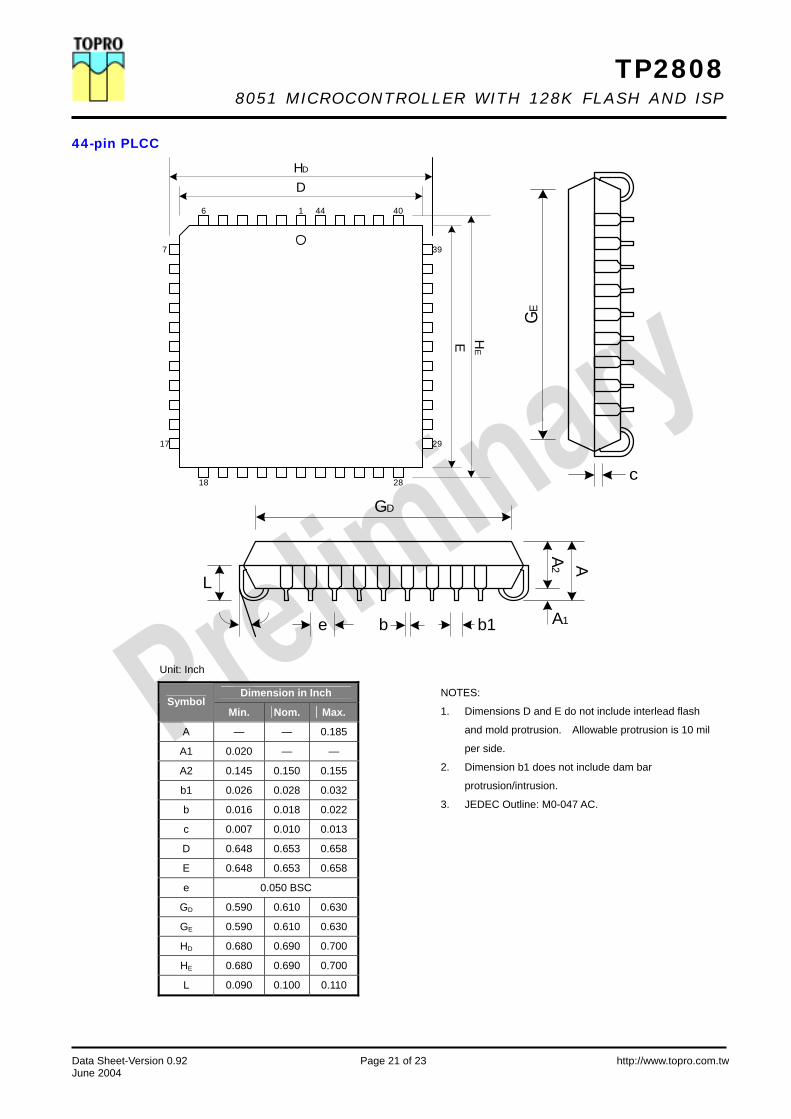
44-pin PLCC
DHD
E HE
6 1 44 40
7
17
18 28
29
39
GE
c
A2 A
GD
A1b1beΘ
L
Unit: Inch
NOTES:
1. Dimensions D and E do not include interlead flash
and mold protrusion. Allowable protrusion is 10 mil
per side.
2. Dimension b1 does not include dam bar
protrusion/intrusion.
3. JEDEC Outline: M0-047 AC.
Dimension in Inch Symbol
Min. Nom. Max.
A — — 0.185
A1 0.020 — —
A2 0.145 0.150 0.155
b1 0.026 0.028 0.032
b 0.016 0.018 0.022
c 0.007 0.010 0.013
D 0.648 0.653 0.658
E 0.648 0.653 0.658
e 0.050 BSC
GD 0.590 0.610 0.630
GE 0.590 0.610 0.630
HD 0.680 0.690 0.700
HE 0.680 0.690 0.700
L 0.090 0.100 0.110

TP28088051 MICROCONTROLLER WITH 128K FLASH AND ISP
Data Sheet-Version 0.92 Page 22 of 23 http://www.topro.com.tw June 2004
44-pin PQFP
Unit: Millimeter
NOTES:
1. Dimensions D and E do not include interlead flash.
2. Dimension b does not include dam bar protrusion/intrusion.
3. JEDEC Outline: MO-108 AA-1.
Dimension in mm Symbol
Min. Nom. Max.
A — — 2.7
A1 0.25 — 0.5
A2 1.9 2.0 2.2
b 0.3 TYP.
c 0.10 0.15 0.20
D 9.9 10.00 10.1
E 9.9 10.00 10.1
e 0.80 TYP.
HD 13 13.2 13.4
HE 13 13.2 13.4
L 0.73 0.88 0.93
L1 — 1.6 —
y 0.10
θ° 0° — 7°

TP28088051 MICROCONTROLLER WITH 128K FLASH AND ISP
Data Sheet-Version 0.92 Page 23 of 23 http://www.topro.com.tw June 2004
◎Headquarters 5 F, No. 10, Prosperity Road 1, Science-Based Industrial Park, Hsinchu, Taiwan 300, R.O.C. Tel.: 886-3-563-2515 Fax: 886-3-564-1728 ◎Taipei Office 2 F, No. 26, Lane 583, Ruiguang Rd., Neihu, Taipei, Taiwan 114, R.O.C. Tel.: 886-2-2627-6222 Fax: 886-2-2657-0256 ◎Shenzhen Office Room 802, Tower A, World Trade Plaza, Fuhong Rd., Futian, Shenzhen, China Tel.: 86-755-8367-9985 Fax: 86-755-8367-9518