Towards Large-Capacity and Cost-Effective Main Memories
147
THESIS FOR THE DEGREE OF DOCTOR OF PHILOSOPHY Towards Large-Capacity and Cost-Effective Main Memories DMITRY KNYAGININ Division of Computer Engineering Department of Computer Science and Engineering CHALMERS UNIVERSITY OF TECHNOLOGY Gothenburg, Sweden 2017
Transcript of Towards Large-Capacity and Cost-Effective Main Memories

THESIS FOR THE DEGREE OF DOCTOR OF PHILOSOPHY
Towards Large-Capacity andCost-Effective Main Memories
DMITRY KNYAGININ
Division of Computer EngineeringDepartment of Computer Science and Engineering
CHALMERS UNIVERSITY OF TECHNOLOGY
Gothenburg, Sweden 2017

Towards Large-Capacity and Cost-Effective Main MemoriesDmitry KnyagininISBN 978-91-7597-563-4
Copyright c© 2017 Dmitry Knyaginin
Series number: 4244in the series Doktorsavhandlingar vid Chalmers tekniska högskolaNy serie (ISSN 0346-718X)
Technical report 142DComputer Architecture Research GroupDivision of Computer Engineering
Department of Computer Science and EngineeringChalmers University of TechnologySE-412 96 Gothenburg, SwedenPhone: +46 (0)31-772 10 00
Author e-mail:[email protected]
Printed by Chalmers ReproserviceGothenburg, Sweden 2017
Towards Large-Capacity and Cost-Effective Main MemoriesDmitry KnyagininDivision of Computer Engineering, Chalmers University of Technology
ABSTRACTLarge, multi-terabyte main memories per processor socket are instrumental to address
the continuously growing performance demands of domains like high-performancecomputing, databases, and big data. It is an important objective to design large-capacitymain memories in a way that maximizes their cost-effectiveness and at the same timeminimizes performance losses caused by cost-effective tradeoffs. This thesis addresses anumber of issues towards this objective.
First, parallel memory protocols, that are key to large main memories, have a limitednumber of pins. This implies that to address future capacities, the protocols wouldhave to multiplex the pins to transfer wider addresses in a greater number of cycles,hurting performance. This thesis contributes with the concept of adaptive row addressing,comprising three techniques, as a general approach to minimize the performance lossesof such cost-effective parallel memory protocols, and, in fact, make them as efficient asan idealized protocol with many enough pins to transfer each address in one cycle.
Second, emerging Storage-Class Memory (SCM) technologies can potentially revolu-tionize main memory design by enabling large-capacity and cost-effective hybrid mainmemories, that combine DRAM and SCM. However, they add multiple dimensions tothe design space of main memories. Detailed exploration of such design spaces solely bymeans of simulation or prototyping is inefficient. This thesis contributes with Crystal, ananalytic method for partitioning hybrid-memory area between DRAM and SCM at designtime, and Rock, a framework for pruning design spaces of hybrid memories. Crystal andRock help system architects to quickly and correctly identify the most promising designpoints for subsequent detailed evaluation.
Third, in hybrid main memories, DRAM is the limited resource, and co-runningprograms compete for it. Fair and at the same time high-performance management ofsuch memories is an important and open issue. To avoid long operating-system overheads,this management has to be performed by hardware. This thesis contributes with ProFess:a Probabilistic hybrid main memory management Framework for high performance andfairness. ProFess includes two hardware-based mechanisms that cooperate to significantlyimprove fairness, performance, and energy-efficiency compared to the state-of-the-art.
Keywords: Large-Capacity Local Memory; Parallel Memory Protocols; Hybrid MainMemory; Design-Space Exploration; Hardware-Based Hybrid Memory Management;Cost-Effectiveness; Fairness; Performance; Energy Efficiency

ii
Preface
Parts of the contributions presented in this thesis have previously been published in thefollowing manuscripts:
• Dmitry Knyaginin, Georgi N. Gaydadjiev, and Per Stenström, “Crystal:A design-time resource partitioning method for hybrid main memory,” inProceedings of the 43rd International Conference on Parallel Processing,Minneapolis, MN, USA, Sept. 2014, pp. 90–100.
• Dmitry Knyaginin, Vassilis Papaefstathiou, and Per Stenström, “Adaptiverow addressing for cost-efficient parallel memory protocols in large-capacitymemories,” in Proceedings of the 2nd International Symposium on MemorySystems, Washington, DC, USA, Oct. 2016, pp. 121–132.
The following manuscripts contain parts of the contributions presented in this thesis andhave been submitted to international conferences:
• Dmitry Knyaginin and Per Stenström, “Rock: A framework for pruning thedesign space of hybrid main memory systems,” Under review since Mar. 2017.
• Dmitry Knyaginin, Vassilis Papaefstathiou, and Per Stenström, “ProFess:A probabilistic hybrid main memory management framework for high perfor-mance and fairness,” Under review since Apr. 2017.
The following manuscript has previously been accepted to a workshop, though is notincluded in this thesis:
• Dmitry Knyaginin, Sally A. McKee, and Georgi N. Gaydadjiev, “A hybridmain memory systems taxonomy,” in Memory Architecture and OrganizationWorkshop, co-located with Embedded Systems Week, Tampere, Finland, Oct.2012, pp. 1–6.
iii

iv PREFACE

Acknowledgments
First of all, I would like to thank my advisor, Per Stenström, for his continuous support,critical feedback, and guidance throughout the years. It has been a privilege learningComputer Architecture research from Per.
A big thank you to Vassilis Papaefstathiou for insightful discussions and successfulcollaboration. His input has been extremely helpful to me.
Jan Jonsson has played a key role in my follow-up meetings throughout the years; I amgrateful to Jan for that. On a non-work note, I thank Jan for his reminders that there existsfilm photography, a hobby that I have put aside for way too long.
I am thankful to Lars Svensson for great discussions and support. His help has been veryimportant to me, especially in the early days of my PhD.
I thank Rolf Snedsböl for managing my teaching duties. Thanks to Rolf, I have had agreat pleasure working in multiple courses together with Jan Jonsson, Roger Johansson,Risat Mahmud Pathan, Fatemeh Ayatolahi, Lars Bengtsson, Lennart Hansson, MadhavanManivannan, Ahsen Ejaz, Beshr Al Nahas, Per Larsson-Edefors, Alen Bardizbanyan, andI ask forgiveness if I forgot to mention someone.
A thank you to Sally McKee and Georgi Gaydadjiev for their input and successfulcollaboration, and to Magnus Själander for his help in the beginning of my PhD.
For help with various mathematical aspects of this thesis, I thank Devdatt Dubhashi,Christos Dimitrakakis, Fredrik Johansson, and Vinay Jethava.
I thank Miquel Pericàs for timely discussions about the last project.
To Jacob Lidman, Bhavishya Goel, and Prajith Ramakrishnan Geethakumari – a Big thankyou for supporting the ttitania cluster. I have used ttitania to run most of my experiments.
Many thanks to all the colleagues with whom I have shared the office rooms over theyears, and who have contributed to the nice, productive atmosphere. Special thanks to
v

vi ACKNOWLEDGMENTS
Alen Bardizbanyan for great humor and to Nadja Holtryd for helping me to improve mySwedish and for her comments about a draft of this thesis.
To everybody at the Department of Computer Science and Engineering – many thanksfor the great environment. Special thanks to Eva Axelsson, Marianne Pleen-Schreiber,Agneta Nilsson, Anna-Lena Karlsson, Malin Nilsson, Tiina Rankanen, Elisabeth KegelAndreasson, Monica Månhammar, Peter Helander, Johan Hansén, Rune Ljungbjörn, KoenLindström Claessen, Gerardo Schneider, Arne Linde, and Johan Karlsson. Cordial thanksto the Computer Graphics group—Markus Billeter, Viktor Kämpe, Dan Dolonius, SverkerRasmuson, Erik Sintorn, and Ulf Assarsson—for all the fun discussions. To Anurag Negi,Alen Bardizbanyan, Vinay Jethava, Madhavan Manivannan, Jacob Sznajdman, VilhelmVerendel, and Katarina Steffenburg – my gratitude for their great friendship.
Finally, I would like to thank my parents, Victoria and Vladimir, and my brother, Oleg,for their unconditional love. I dedicate this thesis to them.
This thesis is based upon work supported by grants from the Swedish Research Council(Vetenskapsrådet) under the Chalmers Adaptable Multicore Processing Project (CHAMPP),from the European Union under the FP7 project EUROSERVER (No: 610456), and fromthe European Research Council (ERC) under the MECCA project (contract 340328).
Dmitry KnyagininGothenburg, April 2017
Contents
Abstract i
Preface iii
Acknowledgments v
Acronyms xv
1 Introduction 11.1 Problem Statements . . . . . . . . . . . . . . . . . . . . . . . . . . . . 31.2 Contributions . . . . . . . . . . . . . . . . . . . . . . . . . . . . . . . 41.3 Thesis Organization . . . . . . . . . . . . . . . . . . . . . . . . . . . . 5
2 Cost-Effective Addressing in Large-Capacity Main Memories 72.1 Background and Motivation . . . . . . . . . . . . . . . . . . . . . . . . 9
2.1.1 DDR4 DRAM Memory System . . . . . . . . . . . . . . . . . 92.1.2 Multi-Cycle Addressing . . . . . . . . . . . . . . . . . . . . . 122.1.3 DDR4-Based Two-Cycle Row Addressing . . . . . . . . . . . . 12
2.2 Adaptive Row Addressing . . . . . . . . . . . . . . . . . . . . . . . . 132.2.1 Row-Address Caching . . . . . . . . . . . . . . . . . . . . . . 132.2.2 Row-Address Prefetching . . . . . . . . . . . . . . . . . . . . 182.2.3 Adaptive Row-Access Scheduling . . . . . . . . . . . . . . . . 21
2.3 Experimental Setup . . . . . . . . . . . . . . . . . . . . . . . . . . . . 242.4 Experimental Results . . . . . . . . . . . . . . . . . . . . . . . . . . . 27
2.4.1 Main Evaluation . . . . . . . . . . . . . . . . . . . . . . . . . 272.4.2 Sensitivity Analysis . . . . . . . . . . . . . . . . . . . . . . . . 31
2.5 Related Work . . . . . . . . . . . . . . . . . . . . . . . . . . . . . . . 332.6 Summary . . . . . . . . . . . . . . . . . . . . . . . . . . . . . . . . . 35
vii

viii CONTENTS
3 Partitioning of Hybrid Memory Area 373.1 Background . . . . . . . . . . . . . . . . . . . . . . . . . . . . . . . . 39
3.1.1 Memory Technologies . . . . . . . . . . . . . . . . . . . . . . 393.1.2 Benefits of Hybrid Main Memory . . . . . . . . . . . . . . . . 403.1.3 Allocation of Main Memory Capacity . . . . . . . . . . . . . . 40
3.2 Crystal . . . . . . . . . . . . . . . . . . . . . . . . . . . . . . . . . . . 413.2.1 Complexity of Equal-Area Partitioning . . . . . . . . . . . . . 413.2.2 Assumptions . . . . . . . . . . . . . . . . . . . . . . . . . . . 413.2.3 Models and Method . . . . . . . . . . . . . . . . . . . . . . . 44
3.3 Experimental Methodology . . . . . . . . . . . . . . . . . . . . . . . . 473.4 Experimental Results . . . . . . . . . . . . . . . . . . . . . . . . . . . 51
3.4.1 Applicability of Crystal . . . . . . . . . . . . . . . . . . . . . . 523.4.2 Validation of Partitionings Produced by Crystal . . . . . . . . . 56
3.5 Related Work . . . . . . . . . . . . . . . . . . . . . . . . . . . . . . . 603.6 Summary . . . . . . . . . . . . . . . . . . . . . . . . . . . . . . . . . 61
4 Pruning of Hybrid Memory Design Space 634.1 Hybrid Memory Design Dimensions . . . . . . . . . . . . . . . . . . . 654.2 Rock . . . . . . . . . . . . . . . . . . . . . . . . . . . . . . . . . . . . 66
4.2.1 Workload Representation . . . . . . . . . . . . . . . . . . . . . 674.2.2 Resource Allocation . . . . . . . . . . . . . . . . . . . . . . . 674.2.3 Data Placement . . . . . . . . . . . . . . . . . . . . . . . . . . 684.2.4 Final Calculations . . . . . . . . . . . . . . . . . . . . . . . . 69
4.3 Experimental Methodology . . . . . . . . . . . . . . . . . . . . . . . . 704.4 Experimental Results . . . . . . . . . . . . . . . . . . . . . . . . . . . 73
4.4.1 Work1 Design-Space Pruning . . . . . . . . . . . . . . . . . . 734.4.2 Work2 Design-Space Pruning . . . . . . . . . . . . . . . . . . 77
4.5 Related Work . . . . . . . . . . . . . . . . . . . . . . . . . . . . . . . 814.6 Summary . . . . . . . . . . . . . . . . . . . . . . . . . . . . . . . . . 82
5 Hardware-Based Management of Hybrid Memory 835.1 Background and Motivation . . . . . . . . . . . . . . . . . . . . . . . . 85
5.1.1 Memory Technologies . . . . . . . . . . . . . . . . . . . . . . 855.1.2 Large-Capacity, Flat, Migrating Memory Managed by Hardware 855.1.3 Baseline Organization . . . . . . . . . . . . . . . . . . . . . . 865.1.4 The Fairness Problem . . . . . . . . . . . . . . . . . . . . . . . 885.1.5 The Performance Problem . . . . . . . . . . . . . . . . . . . . 88
5.2 ProFess . . . . . . . . . . . . . . . . . . . . . . . . . . . . . . . . . . 90

CONTENTS ix
5.2.1 Slowdown Estimation Mechanism . . . . . . . . . . . . . . . . 905.2.2 Migration Decision Mechanism . . . . . . . . . . . . . . . . . 955.2.3 Integration of SEM and MDM . . . . . . . . . . . . . . . . . . 99
5.3 Experimental Setup . . . . . . . . . . . . . . . . . . . . . . . . . . . . 1005.3.1 System Configuration . . . . . . . . . . . . . . . . . . . . . . . 1005.3.2 Workloads . . . . . . . . . . . . . . . . . . . . . . . . . . . . 1035.3.3 Figures of Merit . . . . . . . . . . . . . . . . . . . . . . . . . 104
5.4 Experimental Results . . . . . . . . . . . . . . . . . . . . . . . . . . . 1045.4.1 Single-Program Performance of MDM . . . . . . . . . . . . . . 1045.4.2 Sensitivity Analysis of MDM . . . . . . . . . . . . . . . . . . 1065.4.3 Multi-Program Evaluation of MDM . . . . . . . . . . . . . . . 1075.4.4 Multi-Program Evaluation of ProFess . . . . . . . . . . . . . . 109
5.5 Related Work . . . . . . . . . . . . . . . . . . . . . . . . . . . . . . . 1115.6 Summary . . . . . . . . . . . . . . . . . . . . . . . . . . . . . . . . . 112
6 Conclusion 1136.1 Thesis Contributions . . . . . . . . . . . . . . . . . . . . . . . . . . . 1146.2 Future Work . . . . . . . . . . . . . . . . . . . . . . . . . . . . . . . . 116
Bibliography 118

x CONTENTS

List of Figures
2.1 Simplified organization of one DDR4 die . . . . . . . . . . . . . . . . 92.2 RDIMM with 16 memory devices and 64-bit data bus . . . . . . . . . 112.3 Read latency increase due to two-cycle row addressing . . . . . . . . . 132.4 System-level performance loss due to two-cycle row addressing . . . . 132.5 Address mappings . . . . . . . . . . . . . . . . . . . . . . . . . . . . 142.6 Address-caching schemes R-1, F-31, D-31, and W-31 . . . . . . . . . 152.7 Implementation sketch of address-caching scheme W-31 . . . . . . . . 172.8 Example address-cache miss curves . . . . . . . . . . . . . . . . . . . 192.9 Negative impact of row-address caching on request service order . . . 212.10 Minimum delays experienced by older read request when younger read
request gets serviced first . . . . . . . . . . . . . . . . . . . . . . . . 232.11 Positive impact of row-address caching on request service order . . . . 232.12 Cooperation of adaptive row-access priority policy and row-address
prefetching for best efficiency of FRFCFS and R-1 . . . . . . . . . . . 272.13 Performance of FRFCFS-A . . . . . . . . . . . . . . . . . . . . . . . 292.14 Performance of FRFCFS-AP . . . . . . . . . . . . . . . . . . . . . . 292.15 FRFCFS-A and 31-entry caches vs. FRFCFS-AP and 15-entry caches . 302.16 Page coloring applied to FRFCFS-A(P) and W-31 . . . . . . . . . . . 312.17 Random virtual-to-physical address mapping applied to FRFCFS-A(P)
and W-31 . . . . . . . . . . . . . . . . . . . . . . . . . . . . . . . . . 332.18 11-bit MSPs applied to FRFCFS-A(P) and W-31 . . . . . . . . . . . . 33
3.1 Logical memory hierarchy organizations . . . . . . . . . . . . . . . . 423.2 System modeled . . . . . . . . . . . . . . . . . . . . . . . . . . . . . 423.3 Miss curves of selected programs . . . . . . . . . . . . . . . . . . . . 483.4 Results for hybrids with HDD and mcf/soplex workloads . . . . . . . . 523.5 Results for hybrids with HDD and lbm/sjeng workloads . . . . . . . . 543.6 Results for hybrids III-L and III-H and lbm/sjeng workloads . . . . . . 54
xi

xii LIST OF FIGURES
3.7 Results for hybrids with HDD and CG/sjeng workloads . . . . . . . . 553.8 Color coding for parameter values and their combinations . . . . . . . 583.9 Sensitivity results for hybrid II-L and W4 from lbm/sjeng program set . 583.10 Sensitivity results for hybrid I-L and W4 from lbm/sjeng program set . 593.11 Sensitivity results for hybrid III-L and W4 from lbm/sjeng program set 59
4.1 Proposed system of design dimensions . . . . . . . . . . . . . . . . . 654.2 System with flat hybrid main memory . . . . . . . . . . . . . . . . . . 664.3 Design space of Work1 with UA DRA policy and Set1 in 3D view . . . 744.4 Design space of Work1 with UA DRA policy in two-dimensional view 754.5 Design subspace of Work2 with UA DRA policy and Set1 in 3D view . 784.6 Design subspace of Work2 with LU DRA policy and Set1 in 3D view . 784.7 Design subspace of Work2 with HU DRA policy and Set1 in 3D view . 784.8 Design subspace of Work2 with two DIMMs in total . . . . . . . . . . 794.9 Design subspace of Work2 with three DIMMs in total . . . . . . . . . 794.10 Design subspace of Work2 with four DIMMs in total . . . . . . . . . . 79
5.1 Baseline flat migrating organization of large-capacity hybrid memory . 875.2 Individual program slowdowns under PoM management . . . . . . . . 885.3 Interleaved division into regions . . . . . . . . . . . . . . . . . . . . . 915.4 ST entry and STC organization . . . . . . . . . . . . . . . . . . . . . 965.5 Single-program performance of MDM normalized to PoM . . . . . . . 1055.6 Single-program M1 accesses of MDM normalized to PoM . . . . . . . 1055.7 Single-program STC hit rates under MDM . . . . . . . . . . . . . . . 1055.8 Performance sensitivity to STC size . . . . . . . . . . . . . . . . . . . 1075.9 Sensitivity of STC hit rates to STC size . . . . . . . . . . . . . . . . . 1075.10 Maximum slowdown of MDM normalized to PoM . . . . . . . . . . . 1085.11 Performance of MDM normalized to PoM . . . . . . . . . . . . . . . 1085.12 Energy efficiency of MDM normalized to PoM . . . . . . . . . . . . . 1085.13 Maximum slowdown of ProFess normalized to PoM . . . . . . . . . . 1095.14 Performance of ProFess normalized to PoM . . . . . . . . . . . . . . 1095.15 Energy efficiency of ProFess normalized to PoM . . . . . . . . . . . . 1095.16 Individual program slowdowns under PoM, MDM, and ProFess . . . . 110

List of Tables
2.1 Cases when younger A2 gets issued ahead of older row-access command 222.2 System configuration for evaluation of adaptive row addressing . . . . 252.3 DRAM device parameters for evaluation of adaptive row addressing . . 252.4 Memory scheduling championship programs . . . . . . . . . . . . . . 26
3.1 Program profile format . . . . . . . . . . . . . . . . . . . . . . . . . . 433.2 Parameters and variables in (3.1) to (3.8) . . . . . . . . . . . . . . . . 453.3 Selected single-threaded programs for evaluation of Crystal . . . . . . 473.4 System configuration for evaluation of Crystal . . . . . . . . . . . . . 483.5 Default parameter values for evaluation of Crystal . . . . . . . . . . . 493.6 Characteristics of DRAM revisions F and G . . . . . . . . . . . . . . 493.7 Selected memory-technology characteristics for evaluation of Crystal . 503.8 Hybrids and respective baselines for evaluation of Crystal . . . . . . . 51
4.1 DRA policies . . . . . . . . . . . . . . . . . . . . . . . . . . . . . . . 674.2 Parameters and variables in (4.1) . . . . . . . . . . . . . . . . . . . . 694.3 Selected workloads for evaluation of Rock . . . . . . . . . . . . . . . 714.4 System configuration for evaluation of Rock . . . . . . . . . . . . . . 714.5 Memory-technology access latencies for evaluation of Rock . . . . . . 724.6 Sets of assumed parameter values for sensitivity analysis . . . . . . . . 72
5.1 Flat migrating organizations . . . . . . . . . . . . . . . . . . . . . . . 865.2 Migration algorithms . . . . . . . . . . . . . . . . . . . . . . . . . . 895.3 Per-core SEM counters . . . . . . . . . . . . . . . . . . . . . . . . . 925.4 Experimental estimates of sampling accuracy . . . . . . . . . . . . . . 945.5 Quantized access-counter values . . . . . . . . . . . . . . . . . . . . 975.6 Per-core MDM counters . . . . . . . . . . . . . . . . . . . . . . . . . 975.7 Migration decisions guided by SEM . . . . . . . . . . . . . . . . . . . 99
xiii

xiv LIST OF TABLES
5.8 System configuration for evaluation of ProFess . . . . . . . . . . . . . 1015.9 Individual programs for evaluation of ProFess . . . . . . . . . . . . . 1035.10 Multiprogrammed workloads for evaluation of ProFess . . . . . . . . . 103
Acronyms
3D Three-Dimensional
ACM Address-Cache Miss rate
ACT Activate
APP Adaptive row-access Priority Policy
BLISS Blacklisting memory Scheduler
CA Command/Address
CL Column Latency
CPU Central Processing Unit
CWL Column Write Latency
DDR Double Data Rate
DIMM Dual In-line Memory Module
DRA Design-time Resource Allocation
DRAM Dynamic Random Access Memory
DSE Design-Space Exploration
FRFCFS First-Ready, First-Come-First-Serve
HBM High Bandwidth Memory
HDD Hard Disk Drive
HMC Hybrid Memory Cube
HU High-Utility
IPC Instructions Per Cycle
LLC Last-Level Cache
LPDDR Low Power Double Data Rate
xv

xvi ACRONYMS
LRDIMM Load Reduced Dual In-line Memory Module
LRU Least Recently Used
LSP Least-Significant Portion
LU Low-Utility
MC Memory Controller
MCA Multi-Cycle Addressing
MDM Migration Decision Mechanism
MEA Majority Element Algorithm
MPKI Misses Per Kilo Instruction
MRS Mode Register Set
MSC Memory Scheduling Championship
MSP Most-Significant Portion
NVM Non-Volatile Memory
OS Operating System
PCM Phase-Change Memory
PRE Precharge
QAC Quantized Access-Counter
RD Column Read
RDIMM Registered Dual In-line Memory Module
RDP Run-time Data Placement
ROB Re-Order Buffer
RRAM Resistive Random Access Memory
SATA Serial Advanced Technology Attachment
SB Swap Buffer
SCA Single-Cycle Addressing
SCM Storage-Class Memory
SDR Single Data Rate
SEM Slowdown Estimation Mechanism
SSD Solid-State Disk

xvii
ST Swap-group Table
STC Swap-group Table Cache
UA Utility-Agnostic
UDIMM Unbuffered Dual In-line Memory Module
USIMM Utah Simulated Memory Module
WR Column Write

xviii ACRONYMS

1Introduction
The supply of cost-effective memory devices to computer manufacturers has been oneof the main business drivers for the semiconductor industry since its birth in the 70s [1].Large, multi-terabyte main memories per processor socket address demands of domainslike high-performance computing, databases, and big data. In addition, such memoriesrepresent an attractive solution to significantly reduce costs and energy expenditure inmultinode systems by reducing the total number of nodes (scale-in) and at the same timeincreasing the capacity of each node’s memory (scale-up) [2]. Thus, the design of largeand cost-effective local (per socket) main memories is an important objective, and thethesis at hand tackles a number of issues towards it.
Dynamic Random Access Memory (DRAM) had been addressing continuouslygrowing main memory demands by scaling to higher areal densities at about 4x / 3years [3]. However, in the last decade DRAM scaling has slowed to 2x / 3 years [3], fuelinginterest in memory technologies that promise to scale better due to smaller cell size and/orThree-Dimensional (3D) cell stacking [4]. This has brought NAND Flash—the densestcommercial memory technology, conventionally used for high-performance storage—closer to the processor [5–7], generated a massive body of work about Phase-ChangeMemory (PCM) [8] and Resistive Random Access Memory (RRAM) [9–13], and has lead
1

2 CHAPTER 1. INTRODUCTION
to the introduction of 3D Xpoint [14]. A new term, Storage-Class Memory (SCM), hasbeen introduced to collectively refer to technologies that fit in the density, latency, and cost-per-byte gaps between DRAM and magnetic disk. In order to enjoy the best characteristicsof both DRAM and SCM while hiding their drawbacks, the two technologies can becombined into hybrid main memory. As a result, such main memories can be morecost-effective than DRAM-only memories [5, 15, 16]. Orthogonal to die-density scaling,3D die stacking further increases device densities. For instance, the fourth generation ofparallel Double Data Rate (DDR) memory protocols, named DDR4 [17], has standardized3D die stacking for DRAM and supports up to 512-GB memory modules. 3D die stackingemployed in both DRAM and SCM devices is important for maximizing hybrid mainmemory capacity. Thus, this thesis considers 3D-stacked DRAM devices and 3D-stackedSCM devices as basic building blocks of large-capacity memories.
Large local memories are organized as multiple parallel channels populated withlarge-capacity modules. This organization is remaining key to large capacities, despitethat each conventional channel offers relatively modest bandwidth. For instance, IntelXeon E7-8893 v4 supports up to 3TB of DRAM on four channels with a maximumbandwidth of 25.6GB/s per channel [18, 19]. Emerging protocols like High BandwidthMemory (HBM) [20] and Hybrid Memory Cube (HMC) [21] offer significantly higherbandwidths per channel. However, HBM is designed for tight integration with the hostprocessor via a common interposer, that implies relatively small maximum capacity. Atthe same time, HMC is a point-to-point protocol, and to build large-capacity memoryindividual cubes have to be arranged into a “far memory” network [21], where each hopincurs a significant latency overhead [22], making HMC unattractive for large-capacityapplications. Thus, this thesis considers the conventional parallel memory protocols.
Hybrid main memories replace some of DRAM with SCM. For instance, IntelPurley [23] will have six channels, each accommodating one DRAM and one 3D Xpointmodule instead of two DRAM modules. In terms of topology hybrid memory can beorganized as flat, where DRAM and SCM are directly accessible by the processor [24–29],or as hierarchical, where SCM is accessible only via DRAM [15, 16, 30]. The flatorganization is more flexible than the hierarchical one by allowing the processor tobypass DRAM for accesses to data blocks that, due to specific access patterns, are morebeneficial to be accessed from SCM. Regardless of topology, in terms of policy forpromoting data from SCM to DRAM, hybrid memories can be organized as migrating,where data are moved upon promotion [16, 24, 26–30], or as replicating, where data arecopied [15, 25]. When DRAM capacity is large (e.g., one DRAM module per channel likein Intel Purley [23]), it is beneficial to employ the migrating organization, such that thecapacities of both DRAM and SCM contribute to the total capacity visible to the OperatingSystem (OS). This makes flat, migrating hybrid memories particularly attractive.

1.1. PROBLEM STATEMENTS 3
1.1 Problem StatementsThe thesis at hand tackles the multifaceted question of building large-capacity mainmemory per processor socket such that performance losses due to cost-effective tradeoffsare minimized. The thesis identifies three problems. First, parallel memory protocolslike DDR4 [17], which are key to large main memories, have a limited number of pinsthat have to be used economically for addressing future capacities. Splitting wide rowaddresses into multiple parts causes additional address-transfer cycles, that increase theaverage access latency and consequently hurt performance, particularly in large DRAM-only memories. Thus, this thesis tackles the question of how to address large capacitiesusing the available address pins economically with minimum performance losses.
Second, the large design space of main memories combining DRAM and SCMimplies that design-space exploration via detailed simulation is slow, making it possiblethat the most promising design points are not timely identified, and so reducing theefficiency of system design. In general, the design space includes such parameters asDRAM and SCM densities, areas (e.g., the number of devices), access latencies, and theway DRAM and SCM are organized into hybrid memory, to name a few. Since it is highlyinefficient to compare each design point using detailed simulation, it is important to prunethe design-space using high-level models and thereby quickly identify the most promisingdesign points for subsequent detailed evaluation. Thus, this thesis addresses the questionof how to explore design tradeoffs quickly and correctly via design-space pruning.
Third, in large hybrid memories, naive DRAM allocation among co-running programscan significantly hurt system performance and fairness. In such memories, DRAM is alimited resource and co-running programs compete for it. If a program fails to obtainenough DRAM for its needs, it might experience an excessive slowdown. Thus, forfair execution, it is important to monitor the impact of DRAM allocation on individualprogram slowdowns and to dynamically adjust DRAM allocation such that the maximumslowdown among the programs is minimized. At the same time, for high performance, itis important to dynamically identify data blocks that are beneficial to be accessed fromDRAM and to timely migrate them there. Such migration decisions should be driven byindividual cost-benefit analysis for each pair of blocks in SCM and DRAM, as opposedto a heuristic that can produce naive decisions hurting performance. Thus, the thesis athand tackles the problem of large hybrid memory management such that high fairness isachieved at the same time as high performance.

4 CHAPTER 1. INTRODUCTION
1.2 ContributionsThis thesis addresses the above problems by making the following contributions. First, forcost-effective parallel memory protocols in large-capacity memories, the thesis contributesadaptive row addressing [31] as a general approach to close the performance and energy-efficiency gaps between protocols using multi-cycle row addressing and an idealisticprotocol using single-cycle row addressing. Adaptive row addressing is presented inChapter 2 and combines three techniques:
• row-address caching to reduce the number of address-transfer cycles by exploitingrow-address locality [32, 33], where the thesis proposes 2-way row-address cacheswith a custom organization for high encoding efficiency;
• to alleviate the penalty of address-cache misses the thesis proposes row-addressprefetching; and
• to make the memory-request scheduler aware of variable address-transfer latenciesand thus to eliminate a negative impact of row-address caching on the request-serviceorder, the thesis proposes an adaptive row-access priority policy.
Second, to facilitate complete and accurate design-space exploration for hybrid mainmemories by timely identifying the most promising design points for subsequent detailedevaluation, this thesis contributes two analytic methods, presented in Chapters 3 and 4:
• Crystal [34], a design-time resource partitioning method for quick memory-system areapartitioning between DRAM and SCM through exhaustive search for given workloadsand partitioning goals (e.g., minimize execution time, energy, and cost); and
• Rock, a framework that helps system architects to infer important trends for design-space pruning by mutually considering hybrid-memory design dimensions like the totalmemory-system area, memory-system area partitioning between DRAM and SCM,allocation of the DRAM and SCM capacities among co-running programs, and dataplacement within the allocated capacities.
Lastly, to address the fairness and performance issues in hardware-managed, flat, migrat-ing hybrid memories the thesis contributes ProFess, a Probabilistic hybrid main memorymanagement Framework for high performance and fairness, presented in Chapter 5.ProFess combines two mechanisms:
• a Slowdown Estimation Mechanism (SEM) to dynamically monitor individual programslowdowns in multiprogrammed workloads based on a new approach to proxy perfor-mance via the number of served memory requests and migrations in proposed private(dedicated, one per core) and shared regions of the hybrid memory; and

1.3. THESIS ORGANIZATION 5
• a conceptually new, probabilistic Migration Decision Mechanism (MDM) to predictthe number of accesses to each data block and thereby enable individual cost-benefitanalysis for each pair of blocks in SCM and DRAM for driving migration decisions.
Within ProFess, MDM decides which blocks to move to DRAM for high system perfor-mance, and SEM guides it towards high fairness.
1.3 Thesis OrganizationThe rest of the thesis is organized as follows. The next four chapters describe onecontribution each from motivation to proposal to evaluation: Chapter 2 presents theconcept of adaptive row addressing and the three techniques under its umbrella; Chapters 3and 4 respectively present Crystal and Rock; and Chapter 5 presents ProFess and itstwo key mechanisms, SEM and MDM. Finally, Chapter 6 discusses future work andconcludes the thesis.

6 CHAPTER 1. INTRODUCTION

2Cost-Effective Addressing in
Large-Capacity Main Memories
Parallel DDR protocols with multi-drop buses have been de facto standard main memoryprotocols for about 15 years, and DDR4 [35] is the latest in the line. Although emergingpoint-to-point protocols like Hybrid Memory Cube (HMC) [21] offer significantly higherpeak bandwidths, they fall short in terms of latency in large-capacity memories. Forinstance, HMC devices have to be connected into a “far memory” network to increasecapacity, and each hop adds latency1. Parallel protocols with multi-drop buses donot have this issue; thus they will remain key to large-capacity and still low-latencymain memories [37].
Future memory capacity growth implies wider addresses. However, the address buscurrently implemented in DDR4 has reached the limit of the feasible number of pins forhigh-speed (high-data-rate) parallel protocols: it is the widest bus of the protocol, and
1Based on the state-of-the-art Xilinx SERDES [36], optimistic latency estimates for a 16-lane linkwith 15Gbps lanes are 15-20ns per hop, one way. Assuming 40-50ns internal DRAM latencies, suchlink latencies are inline with the read latencies of a single HMC measured by Gokhale et al. [22].
7

8 CHAPTER 2. COST-EFFECTIVE ADDRESSING
increasing its width would present a connectivity challenge leading to signal integrityissues, routing congestion, pad-limited designs, and increased manufacturing expense [38].The burden of additional address pins would propagate through memory modules andchannels down to the processor, requiring system-level changes. That is, widening theaddress bus would render parallel memory protocols slow and cost-ineffective.
So to meet large-capacity demands, parallel protocols should multiplex the avail-able pins and transfer each address in multiple bus cycles2, implementing Multi-CycleAddressing (MCA). An idealistic protocol labeled DDRid would have the same speed butenough pins to transfer each address in a single bus cycle, implementing Single-CycleAddressing (SCA). Compared to DDRid, MCA protocols can have significantly lowerperformance and energy efficiency, and so it is important to improve them.
This chapter contributes adaptive row addressing as a general approach to close theperformance and energy-efficiency gaps between MCA and idealistic SCA protocols. Itdoes so by combining three techniques. A first technique is row-address caching thatexploits row-address locality [32, 33] to reduce the number of cycles per address transferby caching the most-significant row-address bits. I propose 2-way row-address cacheswith a custom organization for high efficiency. To alleviate the performance penalty ofaddress-cache misses, I propose a second technique: row-address prefetching that is ef-fective yet simple to integrate with state-of-the-art memory schedulers. Further, a detailedanalysis of memory-request scheduling reveals that row-address caching can negativelyimpact the request service order. This holds for state-of-the-art schedulers that reorder rowaccesses using the conventional first-ready policy [39, 40] (for instance, First-Ready, First-Come-First-Serve (FRFCFS) [39, 40] or the Blacklisting memory Scheduler (BLISS) [41],among many others). To eliminate the negative impact, I propose a third technique: anadaptive row-access priority policy that can simply replace the first-ready policy.
I study the effectiveness of the above techniques using a high-speed, cost-effectiveMCA protocol based on DDR4 in large-capacity, low-latency main memories. Theread latency gap between the MCA protocol and DDRid is 7.5% on average and up to12.5%; the system-level performance and energy efficiency gaps are 5.5% on averageand up to 6.5%. My evaluation shows that: i) the proposed 2-way row-address cachesperform nearly as well as fully-associative ones; ii) the benefit of row-address prefetchingexceeds the benefit of doubling the address-cache size; and iii) the adaptive row-accesspriority policy cooperates with row-address prefetching to achieve the best performance.Combined, the three techniques of adaptive row addressing robustly close the gap betweenthe MCA protocol and DDRid.
2Unless stated otherwise, the word “cycle” denotes an address-bus cycle throughout this chapter.

2.1. BACKGROUND AND MOTIVATION 9
Figure 2.1: Simplified organization of one DDR4 die
The rest of this chapter is organized as follows. Section 2.1 presents the backgroundand motivation, Section 2.2 adaptive row addressing, and Section 2.3 describes theexperimental setup. Section 2.4 presents the results, Section 2.5 discusses related work,and Section 2.6 summarizes the chapter.
2.1 Background and Motivation
According to insights by JEDEC member companies, future systems will employ a point-to-point protocol for high bandwidth and a parallel protocol with multi-drop buses forlarge capacity and low latency [37]. Next, Section 2.1.1 provides relevant backgroundinformation on large-capacity memories and DDR4, the latest parallel memory protocol.Section 2.1.2 motivates MCA, and Section 2.1.3 motivates adaptive row addressing.
2.1.1 DDR4 DRAM Memory System
Device Organization A DDR4 device is organized as up to eight 3D-stacked memorydies connected by through-silicon vias. The dies share the Command/Address (CA) busand the data bus. A die contains four bank groups each comprising four banks, as shownin Figure 2.1 [42]. Each bank is organized as a memory array with up to 256K rows and1K columns [35].

10 CHAPTER 2. COST-EFFECTIVE ADDRESSING
Device Operation The precharge command (PRE) prepares the target bank for anactivation and incurs a delay labeled tRP . The activate command (ACT) opens a rowin a bank, i.e., senses the target row into the bank’s row buffer (also known as senseamplifiers). ACT incurs a delay labeled tRCD . Next, the target column is accessed inthe row buffer by column read (RD) or write (WR) commands with respective delaysCL and CWL. The row buffer is accessed in bursts of eight data-bus half-cycles, and soeach column access occupies the data bus for four cycles. Activations are destructive,thus the content of the row buffer has to be restored to the memory array. The restorestarts automatically in the background and its latency is tRAS . Hence, the minimumdelay between consecutive ACTs to the same bank is tRC = tRAS + tRP . The delaybetween consecutive ACTs to different banks in the same bank group is labeled tRRD_L,and that to different banks in different groups is labeled tRRD_S . Because of bankgrouping, tRRD_L > tRRD_S . Likewise, there are two delays between consecutivecolumn accesses: tCCD_L and tCCD_S , where tCCD_L > tCCD_S [35].
Device Address Pins A typical DDR4 device used in large-capacity memories has78 pins in total, half of which are power and ground and four are data pins [42]. Most ofthe remaining pins belong to the CA bus.
The address pins of the CA bus include three Chip-ID pins for addressing the 3D-stacked dies, two bank-group and two bank-address pins for addressing the banks,and 18 pins labeled A[17:0] for row addressing during ACT. Pins A[9:0] aremultiplexed for column addressing within the open row during the column accesscommands (RD or WR).
The row address is significantly wider than the column address (18 vs. 10 bits),and in large-capacity memories this width gap has been growing. That is, the row-address width dictates the CA-bus width. As a result, some of the CA-bus pins areunder-utilized: a detailed analysis reveals that pins A[17] and A[13] are functionallyused only during ACT3.
Channel Organization A parallel memory channel is organized as one or morememory modules that share the CA bus and the data bus. A module is organized asa number of memory devices that share the CA bus, but each device connects to aprivate slice of the data bus. For instance, the Registered Dual In-line Memory Module(RDIMM) [43] in Figure 2.2 [44] holds 16 memory devices each with four data pins
3Pins A[17] and A[13] are used during ACT and Mode Register Set (MRS), but during MRSthey must be set to zero [35] and thus they are not functionally used (i.e., they can be internallyhardwired to zero).

2.1. BACKGROUND AND MOTIVATION 11
Figure 2.2: RDIMM with 16 memory devices (D15-D0) and 64-bit data bus (DQ)
forming a 64-bit data bus (I exclude memory devices and respective additional data-buspins used for error detection and correction, since it is outside the scope of the chapter).
Channel Operation Each die of a memory device operates in lockstep with therespective dies across the other devices of the module forming a rank. For instance, the16 devices in Figure 2.2 with eight dies per 3D stack form eight ranks. The numberof consecutive ACTs to the same rank is limited to four per sliding window tFAW .Consecutive column accesses to different ranks incur a switching delay labeled tRTRS .
Electrical Constraints Unlike the DDR data bus, the CA bus is Single Data Rate(SDR) due to a high electrical load in large-capacity memories, as follows. Each memorydevice appears as a single electrical load regardless of the number of dies per 3D stack,since the bottom die isolates the loads of the other dies. Thus an Unbuffered Dual In-lineMemory Module (UDIMM) [45] with 16 devices appears as 16 loads on the CA busand as one load on each 4-bit slice of the 64-bit data bus. Populating the channel witha second UDIMM doubles the respective numbers of loads. A heavily loaded CA buscan lead to low data rates, since: 1) the maximum operating clock rate (frequency) forreliable transmission on a bus decreases as the number of loads on the bus grows, and2) the clock signal is shared between the CA bus and the data bus. Thus in large-capacity,high-performance memories UDIMMs have been superseded by RDIMMs, that registerthe CA bus as shown in Figure 2.2. An RDIMM appears as a single load on the channel’sCA bus (the pre-register CA bus). However, the number of loads on the RDIMM’s CAbus (the post-register CA bus) is still large, totaling half the number of memory devicesper module. Load Reduced DIMMs (LRDIMMs) register both the CA bus and the databus [46]. Though, they do not reduce the number of loads on the post-register CA bus [47].

12 CHAPTER 2. COST-EFFECTIVE ADDRESSING
Thus, even if RDIMMs or LRDIMMs are employed, the CA bus has a large number ofloads and has to be SDR in order to guarantee the peak data rates.
2.1.2 Multi-Cycle Addressing (MCA)Future memory capacities are expected to grow. For instance, the International TechnologyRoadmap for Semiconductors predicts 3D stacks taller than eight dies [48]. In addition,memory die densities continuously increase [49].
Capacity growth implies wider addresses. However, widening the address bus beyondthat of DDR4 would cause multiple issues manifesting themselves in lower speedsand higher costs [38]. Besides, widening the bus for row addressing would increasethe number of already under-utilized pins. Thus to stay high-speed and cost-effective,parallel memory protocols have to address larger capacities by using the available pinseconomically. In addition, the CA bus has to be SDR in order to comply with the stringentelectrical constraints, required to guarantee the peak data rates (making the CA bus DDRwould reduce its maximum frequency and hence it would slow the data bus). This suggestMCA, where pins are multiplexed to transfer each address in multiple CA-bus cycles.
2.1.3 DDR4-Based Two-Cycle Row AddressingTo avoid costly disruptions of the well-established DDR4 ecosystem, I consider an MCAprotocol that is based on DDR4 and has the same pin count and speed. To support futurelarge capacities while using the available pins economically, I reassign the under-utilizedA[17] and A[13] from row address to Chip ID thus enabling up to 32 dies per 3D stack.Row addresses are transferred over the remaining 16 pins (A[16:14], A[12:0]) intwo cycles4.
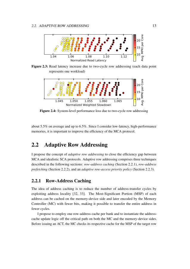
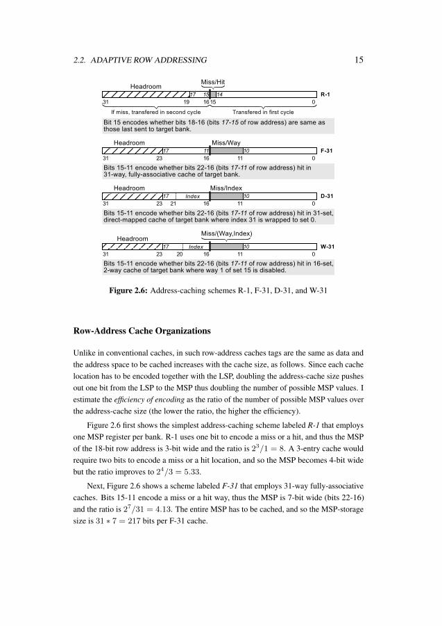
Although some address-transfer cycles can be overlapped with bank-busy cycles, theopportunity to do so is limited. Additional address-transfer cycles interfere with othercommands on the CA bus, causing the MCA protocol to perform significantly worse thanDDRid (the idealistic protocol with enough pins for SCA). Figure 2.3 shows that two-cycle row addressing in 100 multi-program workloads (the experimental setup is describedin Section 2.3) increases the read latency by about 7.5% on average and up to 12.5%.Figure 2.4 shows that two-cycle row addressing reduces the system-level performance by
4An alternative optimization could reassign three pins—A[17], A[13], A[11]—from rowaddress to Chip ID and, e.g., bank address (should the number of banks increase in the future).This optimization affects only MRS and ACT [35]. The MRS opcodes would have to be sent intwo cycles over pins A[12], A[10:0]. However, MRS is used only during initialization. Duringnormal operation, pins A[16:14], A[12], A[10:0] would transfer row addresses in two cycles.I evaluate an equivalent of this optimization as part of sensitivity analysis in Section 2.4.2.
2.2. ADAPTIVE ROW ADDRESSING 13
1.04 1.06 1.08 1.10 1.12Normalized Read Latency
10
15
20
Avg. M
PK
I per
Core
Figure 2.3: Read latency increase due to two-cycle row addressing (each data pointrepresents one workload)
1.045 1.050 1.055 1.060 1.065Normalized Weighted Slowdown
10
15
20
Avg. M
PK
I per
Core
Figure 2.4: System-level performance loss due to two-cycle row addressing
about 5.5% on average and up to 6.5%. Since I consider low-latency, high-performancememories, it is important to improve the efficiency of the MCA protocol.
2.2 Adaptive Row AddressingI propose the concept of adaptive row addressing to close the efficiency gap betweenMCA and idealistic SCA protocols. Adaptive row addressing comprises three techniquesdescribed in the following sections: row-address caching (Section 2.2.1), row-addressprefetching (Section 2.2.2), and an adaptive row-access priority policy (Section 2.2.3).
2.2.1 Row-Address CachingThe idea of address caching is to reduce the number of address-transfer cycles byexploiting address locality [32, 33]. The Most-Significant Portion (MSP) of eachaddress can be cached on the memory-device side and later encoded by the MemoryController (MC) with fewer bits, making it possible to transfer the entire address infewer cycles.
I propose to employ one row-address cache per bank and to instantiate the address-cache update logic off the critical path on both the MC and the memory-device sides.Before issuing an ACT, the MC checks its respective cache for the MSP of the target row

14 CHAPTER 2. COST-EFFECTIVE ADDRESSING
Figure 2.5: Address mappings
address. Upon a hit, it encodes the hit location and sends it to the target bank along withthe Least-Significant Portion (LSP) of the row address, in one cycle. Upon a miss: 1) theMC encodes the miss and sends it with the LSP in one cycle, followed by the MSP in thesecond cycle; and 2) the MC updates its respective cache, and the memory dies of thetarget rank mirror the update in their own respective caches.
Row-address caches are most effective if consecutive memory accesses have thesame MSPs. If MSPs are different, row-address caches can still be effective if the reusedistances [50] of the MSPs are short. In the following sections I discuss row-addresslocality, row-address cache organizations, and their implementation details.
Row-Address Locality
Row-address locality depends on a number of factors: 1) program row-access patterns,2) virtual-to-physical address mapping, 3) physical-to-DRAM address mapping, and4) interference among co-running programs. Figure 2.5 illustrates the virtual-to-physicaland physical-to-DRAM address mappings in a system with a 48-bit virtual address space,8-KB virtual pages (and 8-KB physical frames), four channels, 32 ranks per channel,and 64-B cache blocks5. Figure 2.5 shows a physical-to-DRAM address mapping that isconsidered baseline for the open-page row-buffer management policy [51]. Figure 2.5also shows how the row field (the 18-bit row address) is split into two portions by the 16row-address pins, with bits 41-40 being the MSP.
Virtual-to-physical address mapping is a major factor affecting row-address localitywith two extremes: 1) the OS maps virtual pages to sequential physical frames yieldinghigh locality, and 2) the OS maps pages to random frames yielding low locality. In realsystems, an intermediate amount of row-address locality can be expected.
5The block field (bits 14-8) is 7-bit wide to address each 64-B cache block per aggregate 8-KBrow buffer of 16 banks operating in lockstep, where each bank has a 512-B row buffer.
2.2. ADAPTIVE ROW ADDRESSING 15
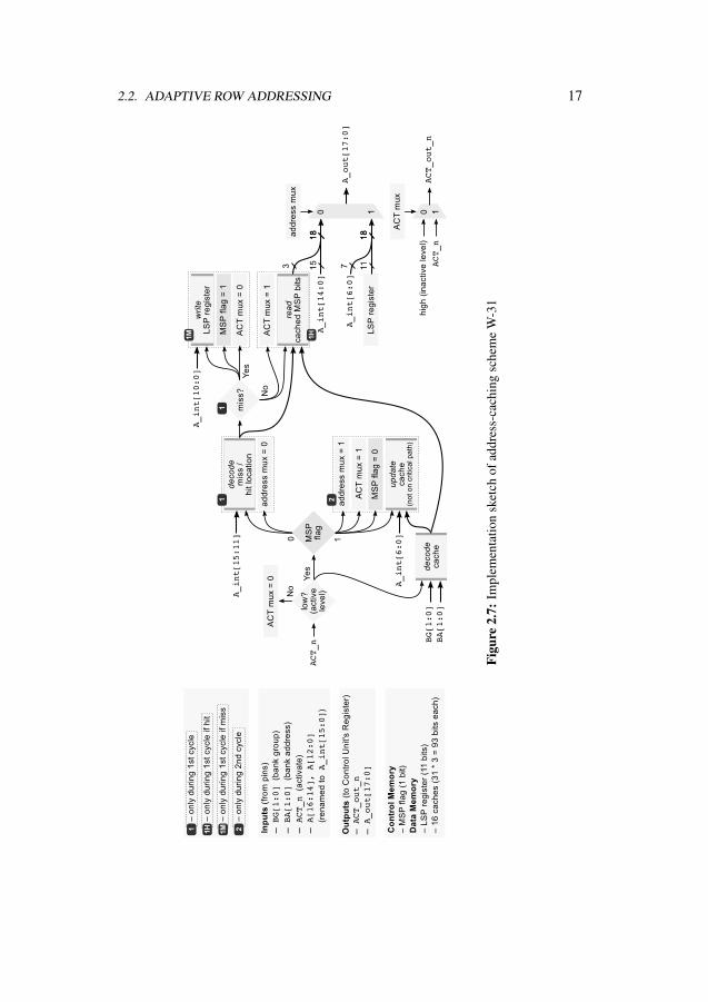
Figure 2.6: Address-caching schemes R-1, F-31, D-31, and W-31
Row-Address Cache Organizations
Unlike in conventional caches, in such row-address caches tags are the same as data andthe address space to be cached increases with the cache size, as follows. Since each cachelocation has to be encoded together with the LSP, doubling the address-cache size pushesout one bit from the LSP to the MSP thus doubling the number of possible MSP values. Iestimate the efficiency of encoding as the ratio of the number of possible MSP values overthe address-cache size (the lower the ratio, the higher the efficiency).
Figure 2.6 first shows the simplest address-caching scheme labeled R-1 that employsone MSP register per bank. R-1 uses one bit to encode a miss or a hit, and thus the MSPof the 18-bit row address is 3-bit wide and the ratio is 23/1 = 8. A 3-entry cache wouldrequire two bits to encode a miss or a hit location, and so the MSP becomes 4-bit widebut the ratio improves to 24/3 = 5.33.
Next, Figure 2.6 shows a scheme labeled F-31 that employs 31-way fully-associativecaches. Bits 15-11 encode a miss or a hit way, thus the MSP is 7-bit wide (bits 22-16)and the ratio is 27/31 = 4.13. The entire MSP has to be cached, and so the MSP-storagesize is 31 ∗ 7 = 217 bits per F-31 cache.

16 CHAPTER 2. COST-EFFECTIVE ADDRESSING
The third scheme in Figure 2.6 is labeled D-31 and employs 31-set direct-mappedcaches. Upon a miss, the caches are indexed by bits 20-16, and since the number of setsis not a power of two, index 31 is wrapped to set 0. Since MSPs with different bits 20-16(index 31 and index 0) can map to set 0, the entire MSP has to be cached. Thus, theMSP-storage size of D-31 is the same as that of F-31. Making the number of sets a powerof two simplifies indexing but reduces the efficiency of encoding: like F-31, D-31 hasthe ratio of 27/31 = 4.13, but a scheme with 32-set direct-mapped caches would have amuch worse ratio of 28/32 = 8.
The last scheme in Figure 2.6 is labeled W-31 and employs 31-entry, 2-way set-associative caches. The number of sets is 16 which simplifies indexing, and to achieve thesame encoding efficiency as D-31 and F-31, I propose to disable the second way of thelast set and use the all-ones combination to encode a miss. Thus upon a hit, bit 15 encodesthe hit way and bits 14-11 the hit set, and in set 15 only the first way can be addressed.Upon a miss, bits 15-11 are set to one. W-31 requires a smaller MSP storage than F-31and D-31, since MSPs with different bits 19-16 map to unique sets. That is, bits 19-16come directly from the hit-set index (bits 14-11) and only three bits of the MSP (bits22-20) have to be cached, reducing the MSP-storage size to 31 ∗ 3 = 93 bits per W-31cache. Thus the advantages of the proposed W-31 are simplicity, high encoding efficiency,small MSP storage, and a conflict-miss rate likely between those of F-31 and D-31.
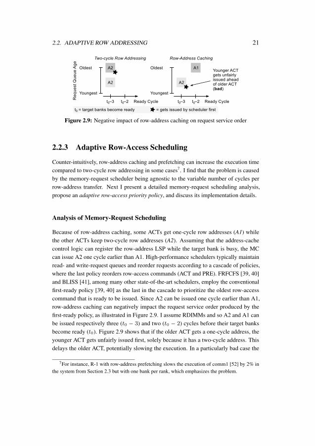
Implementation Details
On the device side, I instantiate row-address caches right before the Control Unit’sCommand/Address Register (recall Figure 2.1). Figure 2.7 shows an implementationsketch of W-31. For brevity, I rename pins A[16:14], A[12:0] to A_int[15:0].
Upon an address-cache miss, the row address is a concatenation of seven bits sent bythe MC in the second address-transfer cycle (A_int[6:0]) and 11 LSP bits registeredat the first address-transfer cycle (block 1M in Figure 2.7). Upon an address-cache hit,the row address is a concatenation of three cached MSP bits (block 1H in Figure 2.7) and15 bits sent by the MC (A_int[14:0]).
The circuit operates transparently to the Control Unit (no changes to the Control Unitare needed). The row-address caches are tiny, and so decoding the hit location and readingout the MSP can be performed very fast, without a performance penalty on the SDR CAbus. The MSP-storage overhead is trivial and is dwarfed by the area of the banks.
2.2. ADAPTIVE ROW ADDRESSING 17
Figu
re2.
7:Im
plem
enta
tion
sket
chof
addr
ess-
cach
ing
sche
me
W-3
1

18 CHAPTER 2. COST-EFFECTIVE ADDRESSING
2.2.2 Row-Address Prefetching
The tiny size of row-address caches suggests that they might have high miss rates. In thefollowing sections I discuss the miss rates, propose row-address prefetching to reducethem, and describe its implementation.
Address-Cache Miss Rates
I collect Least Recently Used (LRU) stack-distance histograms using Mattson’s algo-rithm [50] at the granularity of one cache block (64B) for single-program workloads andthe system from Section 2.3 but with just one bank per rank. I consider MSP widths from3 to 9 bits that yield, respectively, 1 to 7 bits to encode a miss or a hit location. Thus, thelargest possible address-cache sizes are 1 to 127 entries.
To illustrate the miss rates, Figure 2.8 shows the miss curves of comm2 from theMemory Scheduling Championship (MSC) suite [52] for one of the banks (the misscurves for the other banks are very similar). The markers indicate the miss rates of thelargest possible row-address caches for the respective MSP widths, i.e., the best missrates. For instance, Figure 2.8a shows that when the virtual-to-physical mapping issequential (the first extreme, yielding high locality) all of the MSP values can be cached,except when the MSP is 3-bit wide: then the best miss rate is 20%. Figure 2.8b showsthat when the MSC frame numbers [52] are used, the best miss rate is about 50% forthe 3-bit MSP (1-entry row-address cache) and about 5% for the 7-bit MSP (31-entryrow-address cache). Figure 2.8c shows that when frames are allocated randomly (thesecond extreme, yielding low locality) the best miss rates increase dramatically. TheMSC frame numbers [52] exhibit an intermediate amount of row-address locality that canbe expected in real systems.
When the program is executed in a multi-program workload, the miss rates are likelyto increase due to interference. Next I describe row-address prefetching, a technique toalleviate the penalty of address-cache misses.
Row-Address Prefetch Strategy
I propose row-address prefetching and implement it in the memory-request scheduler. Idefine a row-address prefetch as a command that transfers a request’s row-address MSPto the row-address cache of its target bank.
Schedulers maintain request queues, where the oldest request is the one that gotenqueued first. The next command for each request depends on the status of its targetbank and can be ACT, PRE, RD or WR. Memory timing constraints define whether a

2.2. ADAPTIVE ROW ADDRESSING 19
20 21 22 23 24 25 26 27
Row-Address Cache Size (Entries)
0
20
40
60
80
100
Mis
s R
ate
(%
)MSPwidth(bits)
3
4
5
6
7
8
9
(a) Sequential address mapping
20 21 22 23 24 25 26 27
Row-Address Cache Size (Entries)
0
20
40
60
80
100
Mis
s R
ate
(%
)
MSPwidth(bits)
3
4
5
6
7
8
9
(b) MSC frame numbers [52]
20 21 22 23 24 25 26 27
Row-Address Cache Size (Entries)
0
20
40
60
80
100
Mis
s R
ate
(%
)
MSPwidth(bits)
3
4
5
6
7
8
9
(c) Random address mapping
Figure 2.8: Address-cache miss curves of comm2 [52]. Markers show best miss rates forrespective MSP widths

20 CHAPTER 2. COST-EFFECTIVE ADDRESSING
command can be issued at a specific CA-bus cycle. A row-address prefetch can be issuedat an idle cycle, i.e., if no other command can be issued at that cycle6.
I propose the following prefetch strategy. The scheduler tracks banks that are eligiblefor prefetch, and initially all banks are flagged as eligible. A bank is flagged as ineligibleif the oldest request to that bank has a one-cycle row address and its next command isACT or PRE. A prefetch is permitted for a request if: 1) its target bank is flagged aseligible and 2) the request has a two-cycle row address and its next command is ACTor PRE. All permitted prefetches are prioritized first by command (requests whose nextcommand is ACT get the high priority) and then by age (the oldest request gets the highpriority). At an idle CA-bus cycle, the prefetch with the highest priority is issued. Thisway I prefetch for as many requests as possible and avoid prefetch interference per bank,i.e., address-cache interference of later prefetches with earlier ones. This strategy isan efficient tradeoff between the simplest strategy that prefetches for the oldest request(regardless of the target bank) and the finest-grain strategy that tracks address-cache setseligible for prefetch (and so avoids prefetch interference per set).
Implementation Details
The protocol has to have a reserved command available. For instance, DDR4 has onereserved command [35] and MSPs up to 13 bits can be sent over pins A[12:0]. Theprefetch command is executed only by the address-cache control logic. An extensionof the sketch in Figure 2.7 is straightforward: upon a prefetch command, update therow-address cache using A_int[6:0]. The storage overhead is one bit per bank to flagbanks eligible for prefetch.
The proposed row-address prefetching is easy to integrate with state-of-the-artschedulers. For instance, BLISS [41] temporarily blacklists programs that recently issuedfour consecutive column accesses and prioritizes non-blacklisted programs. This simplyadds one priority level to the proposed prefetch strategy: all permitted prefetches are firstprioritized by program (requests of non-blacklisted programs get the high priority), thenby command, and lastly by age.
6Idle cycles are expected since the CA bus is never utilized more than the data bus. Each requestoccupies the data bus for four cycles. Upon a row-buffer miss (PRE + ACT + RD/WR), a requestwith a two-cycle row address occupies the CA bus for four cycles. However, a request with aone-cycle row address occupies the CA bus for three cycles. Upon a row-buffer hit (RD/WR), eachrequest occupies the CA bus for only one cycle. Hence, there is at least one idle CA-bus cycle perrequest with a one-cycle row address.
2.2. ADAPTIVE ROW ADDRESSING 21
Figure 2.9: Negative impact of row-address caching on request service order
2.2.3 Adaptive Row-Access Scheduling
Counter-intuitively, row-address caching and prefetching can increase the execution timecompared to two-cycle row addressing in some cases7. I find that the problem is causedby the memory-request scheduler being agnostic to the variable number of cycles perrow-address transfer. Next I present a detailed memory-request scheduling analysis,propose an adaptive row-access priority policy, and discuss its implementation details.
Analysis of Memory-Request Scheduling
Because of row-address caching, some ACTs get one-cycle row addresses (A1) whilethe other ACTs keep two-cycle row addresses (A2). Assuming that the address-cachecontrol logic can register the row-address LSP while the target bank is busy, the MCcan issue A2 one cycle earlier than A1. High-performance schedulers typically maintainread- and write-request queues and reorder requests according to a cascade of policies,where the last policy reorders row-access commands (ACT and PRE). FRFCFS [39, 40]and BLISS [41], among many other state-of-the-art schedulers, employ the conventionalfirst-ready policy [39, 40] as the last in the cascade to prioritize the oldest row-accesscommand that is ready to be issued. Since A2 can be issued one cycle earlier than A1,row-address caching can negatively impact the request service order produced by thefirst-ready policy, as illustrated in Figure 2.9. I assume RDIMMs and so A2 and A1 canbe issued respectively three (t0 − 3) and two (t0 − 2) cycles before their target banksbecome ready (t0). Figure 2.9 shows that if the older ACT gets a one-cycle address, theyounger ACT gets unfairly issued first, solely because it has a two-cycle address. Thisdelays the older ACT, potentially slowing the execution. In a particularly bad case the
7For instance, R-1 with row-address prefetching slows the execution of comm1 [52] by 2% inthe system from Section 2.3 but with one bank per rank, which emphasizes the problem.
22 CHAPTER 2. COST-EFFECTIVE ADDRESSING
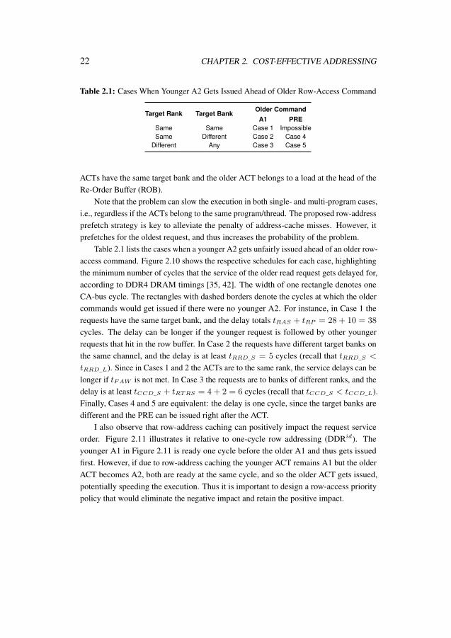
Table 2.1: Cases When Younger A2 Gets Issued Ahead of Older Row-Access Command
Target Rank Target BankOlder Command
A1 PRESame Same Case 1 ImpossibleSame Different Case 2 Case 4
Different Any Case 3 Case 5
ACTs have the same target bank and the older ACT belongs to a load at the head of theRe-Order Buffer (ROB).
Note that the problem can slow the execution in both single- and multi-program cases,i.e., regardless if the ACTs belong to the same program/thread. The proposed row-addressprefetch strategy is key to alleviate the penalty of address-cache misses. However, itprefetches for the oldest request, and thus increases the probability of the problem.
Table 2.1 lists the cases when a younger A2 gets unfairly issued ahead of an older row-access command. Figure 2.10 shows the respective schedules for each case, highlightingthe minimum number of cycles that the service of the older read request gets delayed for,according to DDR4 DRAM timings [35, 42]. The width of one rectangle denotes oneCA-bus cycle. The rectangles with dashed borders denote the cycles at which the oldercommands would get issued if there were no younger A2. For instance, in Case 1 therequests have the same target bank, and the delay totals tRAS + tRP = 28 + 10 = 38
cycles. The delay can be longer if the younger request is followed by other youngerrequests that hit in the row buffer. In Case 2 the requests have different target banks onthe same channel, and the delay is at least tRRD_S = 5 cycles (recall that tRRD_S <
tRRD_L). Since in Cases 1 and 2 the ACTs are to the same rank, the service delays can belonger if tFAW is not met. In Case 3 the requests are to banks of different ranks, and thedelay is at least tCCD_S + tRTRS = 4 + 2 = 6 cycles (recall that tCCD_S < tCCD_L).Finally, Cases 4 and 5 are equivalent: the delay is one cycle, since the target banks aredifferent and the PRE can be issued right after the ACT.
I also observe that row-address caching can positively impact the request serviceorder. Figure 2.11 illustrates it relative to one-cycle row addressing (DDRid). Theyounger A1 in Figure 2.11 is ready one cycle before the older A1 and thus gets issuedfirst. However, if due to row-address caching the younger ACT remains A1 but the olderACT becomes A2, both are ready at the same cycle, and so the older ACT gets issued,potentially speeding the execution. Thus it is important to design a row-access prioritypolicy that would eliminate the negative impact and retain the positive impact.

2.2. ADAPTIVE ROW ADDRESSING 23
Figure 2.10: Minimum delays experienced by older read request when younger readrequest gets serviced first
Figure 2.11: Positive impact of row-address caching on request service order

24 CHAPTER 2. COST-EFFECTIVE ADDRESSING
Adaptive Row-Access Priority Policy
I propose an Adaptive row-access Priority Policy (APP) as follows. Since the servicedelays in Cases 1 to 3 are significant, I propose to postpone the younger A2 (that is, tonot issue it at the current cycle) if there is an older A1 that will be ready at the next cycle.However, in Cases 4 and 5 there is a tradeoff. If I issue the A2, the service delay of thePRE is just one cycle. If I postpone the A2, its service delay would be two cycles. Thus, Ipropose to not postpone a younger A2 if there is an older PRE that will be ready at thenext cycle.
To summarize, APP prioritizes an older A1 ready at the next cycle over a youngerA2 ready at the current cycle, regardless whether the ACTs have the same target bank.I find that this single change to the first-ready policy eliminates the negative impact ofrow-address caching.
The address-cache miss rate can be reduced by prioritizing a younger A1 over anolder A2 ready at the same cycle. However, this would eliminate the positive impact ofrow-address caching (Figure 2.11) and could slow the execution. Thus, there is no benefitto reduce the address-cache miss rate via scheduling beyond what APP already does.
Note that in the simplest case the MC could ignore the opportunity to issue A2 onecycle earlier than A1. This would avoid the negative impact of row-address caching at thecost of missing the opportunity to overlap the second address-transfer cycle of A2 with abank-busy cycle. That is, it would diminish the benefit of adaptive row addressing. Onthe contrary, APP helps to exploit its full potential.
Implementation Details
The proposed APP can be used in state-of-the-art schedulers by simply replacing thefirst-ready policy. For instance, BLISS [41] prioritizes requests first by program (non-blacklisted programs get the high priority), then by column access, and finally by rowaccess, using the first-ready policy for both column and row accesses. The implementationof APP in BLISS is straightforward: 1) prioritize an older A1 of a non-blacklisted programready at the next cycle over a younger A2 ready at the current cycle, regardless if itsprogram is blacklisted or not; and 2) prioritize an older A1 of a blacklisted program readyat the next cycle over a younger A2 of a blacklisted program ready at the current cycle.
2.3 Experimental SetupI evaluate adaptive row addressing using a detailed memory system simulator USIMM [53],employed in recent memory-system research [54–57]. I extend USIMM with: 1) the
2.3. EXPERIMENTAL SETUP 25
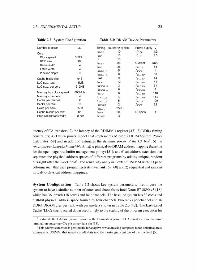
Table 2.2: System Configuration
Number of cores 32
Core:Clock speed 3.2GHzROB size 160Retire width 4Fetch width 4Pipeline depth 10
Cache block size 64BLLC size, total 16MBLLC size, per core 512KB
Memory bus clock speed 800MHzMemory channels 4Ranks per channel 2Banks per rank 16Rows per bank 256KCache blocks per row 128Physical address width 38 bits
Table 2.3: DRAM Device Parameters
Timing (800MHz cycles) Power supply (V)tRCD 10 VDD 1.2tRP 10 VPP 2.5CL 10tRAS 28 Current (mA)tRC 38 IDD0 58tRRD_S 5 IPP0 4tRRD_L 6 IDD2P 30CWL 9 IDD2N 44tWR 12 IDD3P 44tWTR_S 2 IDD3N 61tWTR_L 6 IPPSB 3tRTP 6 IDD4R 140tCCD_S 4 IDD4W 144tCCD_L 5 IDD5 190tRTRS 2 IPP5 22tREFI 6240tRFC 208 DQ pins 4tFAW 16
latency of CA transfers; 2) the latency of the RDIMM’s register [43]; 3) DDR4 timingconstraints; 4) DDR4 power model that implements Micron’s DDR4 System PowerCalculator [58] and in addition estimates the dynamic power of the CA bus8; 5) therow:rank:bank:block:channel:block_offset physical-to-DRAM address mapping (baselinefor the open-page row-buffer management policy) [51]; and 6) an address extension thatseparates the physical address spaces of different programs by adding unique, randombits right after the block field9. For sensitivity analysis I extend USIMM with: 1) pagecoloring such that each program gets its own bank [59, 60] and 2) sequential and randomvirtual-to-physical address mappings.
System Configuration Table 2.2 shows key system parameters. I configure thesystem to have a similar number of cores and channels as Intel Xeon E7-8890 v3 [18],which has 36 threads (18 cores) and four channels. The baseline system has 32 cores anda 38-bit physical address space formed by four channels, two ranks per channel and 16DDR4 DRAM dies per rank with parameters shown in Table 2.3 [42]. The Last-LevelCache (LLC) size is scaled down accordingly to the scaling of the program execution for
8I estimate the CA-bus dynamic power as the termination power of CA transfers. I use the sametermination power per CA pin as per data pin [58].
9This address extension is pessimistic for adaptive row addressing compared to the default addressextension of USIMM, that inserts core-ID bits into the most-significant bits of the row field [53].

26 CHAPTER 2. COST-EFFECTIVE ADDRESSING
Table 2.4: MSC Programs [52]
PARSEC MPKI BioBench MPKI Intel Commercial MPKIblack (blackscholes) 3.2 mummer 20.4 comm1 6.9face (facesim) 6.2 tigr 27.4 comm2 8.5ferret 6.7 comm3 3.5fluid (fluidanimate) 3.0 SPEC CPU2006 comm4 2.4freq (freqmine) 3.0 leslie (leslie3d) 6.4 comm5 1.6stream (streamcluster) 3.7 libq (libquantum) 14.0swapt (swaptions) 3.5
simulation [52]. The system uses 8-KB OS pages, the default USIMM virtual-to-physicaladdress mapping (the MSC frame numbers [52]), and the pessimistic address extensiondescribed above. The MC employs one read-request queue and one write-request queueper channel, FRFCFS for each queue, and the default USIMM policy for write-request-queue draining. The write-request queue size, high and low watermarks are 96, 60 and20, respectively.
Workloads Table 2.4 shows the single-threaded programs from the MSC suite [52],where MPKI denotes the number of read Misses in the LLC Per Kilo Instruction. Usingthe programs I generate 100 unique, random, 32-program workloads with a uniformdistribution of the average MPKI per core from 5 to 25.
Scaling Method The program address spaces are limited to 32 bits [52, 53]. Thusa 32-program workload would exercise only 32 + 5 = 37 address bits. Since thebaseline system has a 38-bit physical address space, the most-significant bit of all rowaddresses would be fixed (e.g., zero). To make the evaluation pessimistic for adaptiverow addressing, I inflate the workload address space using the following method: I insert∆ = wPA − wWA zero bits into the least-significant bits of the row field, where wPA isthe physical address space width and wWA is the workload address space width. Thus, Iinsert one zero bit to scale the 37-bit workload address space up to 38 bits. Note that forrandom virtual-to-physical address mapping such scaling is not needed.
System-Level Metrics I assess weighted speedup [61], execution energy, and fair-ness [61]. Weighted speedup is given by
∑i
(IPCMP
i /IPCSPi)
for all programs i inthe workload, where IPCMP
i denotes the Instructions Per Cycle (IPC) of program i
when it is executed in the workload, and IPCSPi when it is executed alone. Since Iconsider performance loss compared to DDRid, I express it as normalized weightedslowdown, i.e., as the weighted speedup of DDRid over that of two-cycle or adaptive row

2.4. EXPERIMENTAL RESULTS 27
R-1 R-1 R-1 R-1
0
20
40
60
80
100
Tw
o-C
ycl
e R
ow
Addr.
(%
)
(a) ACM
A2R-1 R-1 R-1 R-1
0.99
1.00
1.01
1.02
1.03
1.04
1.05
1.06
1.07
Norm
. M
ax S
low
dow
n(b) Fairness
Figure 2.12: Cooperation of APP and row-address prefetching for best efficiency ofFRFCFS and R-1
addressing. Execution energy is estimated by the USIMM system energy model with myextensions described above. Fairness is estimated as the maximum slowdown across theprograms in the workload, given by maxi
(IPCSPi /IPCMP
i
).
Non-System-Level Metrics I consider the read-request latency and Address-CacheMiss rate (ACM), estimated as the percentage of two-cycle row addresses among all rowaddresses transferred. Each metric is averaged across the channels.
2.4 Experimental ResultsI evaluate two-cycle row addressing (A2) and adaptive row addressing with variousaddress-caching schemes and schedulers built on FRFCFS and BLISS (APP adds suffix -Aand row-address prefetching adds suffix -P). Performance, energy, and fairness resultsare normalized to those of DDRid. Next, Section 2.4.1 presents the main evaluation andSection 2.4.2 the sensitivity analysis.
2.4.1 Main Evaluation
Benefit of APP
Figure 2.12 presents the ACM and fairness of A2 and R-1 employing the four possibleversions of FRFCFS: baseline, FRFCFS-A (with APP), FRFCFS-P (with row-addressprefetching), and FRFCFS-AP (with both APP and prefetching). The box plots [62]summarize the results for each configuration across 100 workloads from Section 2.3.
28 CHAPTER 2. COST-EFFECTIVE ADDRESSING
Figure 2.12a shows that FRFCFS-A slightly reduces the ACM spread comparedto FRFCFS. This is because APP prioritizes some of the one-cycle row addresses.FRFCFS-P further reduces the ACM spread and mean. However, the lowest ACM isachieved by FRFCFS-AP, that combines APP and row-address prefetching.
Figure 2.12b shows that the ACM improvements correlate well with fairness gains.FRFCFS-P reduces the ACM but increases the probability of the negative impact ofrow-address caching on the request service order. APP eliminates the negative impact,and so FRFCFS-AP achieves the best fairness for R-1. Recall also that APP eliminatesthe negative impact in both single- and multi-program workloads. Thus, APP is a keytechnique to exploit the full potential of adaptive row addressing via cooperation withrow-address prefetching. For brevity, I further present results only with APP.
Performance of FRFCFS-A
FRFCFS-A employs APP but not row-address prefetching. Figure 2.13 presents nor-malized weighted slowdown of A2, R-1, and various schemes with row-address cachesof three to 63 entries: direct-mapped (D-3 to D-63), 2-way (W-3 to W-63), and fully-associative (F-3 to F-63). The W-* and F-* caches are LRU-managed. Figure 2.13shows that the performance gap between A2 and DDRid (the 1.00 guide line) is about5.5% on average and up to 6.5%. The gap is significant because: i) the opportunityto overlap address-transfer cycles with bank-busy cycles is limited, and ii) additionaladdress-transfer cycles interfere with other commands on the CA bus.
Figure 2.13 shows that FRFCFS-A significantly improves performance: the row-address caches with 15 or more entries perform within 1% of DDRid. Counter-intuitively,for some workloads the MCA protocol performs even better than DDRid (see the pointsbelow the 1.00 guide line). I find that FRFCFS-A significantly reduces the number oftwo-cycle row addresses and the positive impact of the remaining two-cycle addresses onthe request service order outweighs the overhead of the extra address-transfer cycles.
Next, Figure 2.13 shows that the W-* row-address caches perform almost as well asthe respective F-* caches. For instance, both W-31 and F-31 achieve performance within0.5% of DDRid. Hence, there is no clear benefit from associativity above two.
Performance of FRFCFS-AP
FRFCFS-AP employs both APP and row-address prefetching. Figure 2.14 shows that thelatter further improves performance. For instance, R-1 in Figure 2.14 outperforms D-3in Figure 2.13. Likewise, D-15, W-15, and F-15 in Figure 2.14 respectively outperformD-63, W-31, and F-31 in Figure 2.13. Thus, FRFCFS-AP outperforms FRFCFS-A withtwo or more times larger row-address caches. In other words, the benefit of row-address

2.4. EXPERIMENTAL RESULTS 29
A2R-1 D-3 D-7
D-15D-3
1D-6
3W
-3W
-7W
-15W
-31W
-63
F-3
F-7
F-15
F-31
F-63
0.99
1.00
1.01
1.02
1.03
1.04
1.05
1.06
1.07
Norm
. W
eig
hte
d S
low
dow
n
Figure 2.13: FRFCFS-A – Performance
R-1 D-3 D-7D-1
5D-3
1D-6
3W
-3W
-7W
-15W
-31W
-63
F-3
F-7
F-15
F-31
F-63
0.99
1.00
1.01
1.02
1.03
Norm
.W
eig
hte
dSlo
wdow
n
Figure 2.14: FRFCFS-AP – Performance
prefetching exceeds the benefit of doubling the address-cache size. I consider 31-entryrow-address caches as a reasonable design point. Although smaller caches also performwell, they lack robustness, as I discuss in Section 2.4.2.
Detailed Results for FRFCFS-A(P)
I find that the read-request latency of A2 is longer than that of DDRid by 7.5% on averageand up to 12.5% (Figure 2.3). FRFCFS-A and FRFCFS-AP improve the read-requestlatency in much the same way as they improve the system performance in Figures 2.13and 2.14. For brevity, I omit the read-latency plots.
Figure 2.15 presents detailed results for A2 and D-31, W-31, F-31 using FRFCFS-Avs. D-15, W-15, F-15 using FRFCFS-AP. Figure 2.15a shows that row-address prefetch-ing significantly reduces the ACM spread: the 15-entry row-address caches usingFRFCFS-AP achieve a two times smaller ACM spread compared to the respective 31-entry caches using FRFCFS-A. Figures 2.15b, 2.15c and 2.15d show that thanks to thesmaller ACM spread, the 15-entry caches outperform the respective 31-entry caches interms of system-level performance, execution energy, and fairness. This emphasizes thebenefit of row-address prefetching.

30 CHAPTER 2. COST-EFFECTIVE ADDRESSING
D-31W
-31
F-31
D-15W
-15
F-15
0
5
10
15
20
25
Tw
o-C
ycl
e R
ow
Addr.
(%
)
(a) ACM
A2D-3
1W
-31
F-31
D-15W
-15
F-15
0.98
1.00
1.02
1.04
1.06
Norm
. W
eig
hte
d S
low
dow
n
(b) Performance
A2D-3
1W
-31
F-31
D-15W
-15
F-15
0.98
1.00
1.02
1.04
1.06
Norm
. Execu
tion E
nerg
y
(c) Energy
A2D-3
1W
-31
F-31
D-15W
-15
F-15
0.98
1.00
1.02
1.04
1.06
Norm
. M
ax S
low
dow
n
(d) Fairness
Figure 2.15: FRFCFS-A and 31-entry caches vs. FRFCFS-AP and 15-entry caches
Figure 2.15c shows that F-31, W-15, and F-15 have lower system-level executionenergies than DDRid for half of the workloads (the medians rest on the 1.00 guide line).The energy-efficiency gain over DDRid is due to: 1) the narrower CA bus and 2) thepositive impact of row-address caching on the request service order.
The fairness results in Figure 2.15d are similar to the results in Figures 2.15band 2.15c, though the spread is larger. Still, FRFCFS-AP closes the fairness gap betweenA2 and DDRid from 5% on average to less than 1%.
Results for BLISS-A and BLISS-AP
I find that the normalized results for BLISS-A(P) are very similar to the respective resultsfor FRFCFS-A(P), and so I omit them for brevity. Despite that BLISS truncates longsequences of row-buffer hits (to improve fairness) [41] and thus can cause more ACTs,

2.4. EXPERIMENTAL RESULTS 31
W-3
1W
-31
0
2
4
6
8
10
Tw
o-C
ycl
e R
ow
Addr.
(%
)
(a) ACM
A2W
-31W
-31
0.96
0.98
1.00
1.02
1.04
1.06
1.08
1.10
Norm
. W
eig
hte
d S
low
dow
n
(b) Performance
A2W
-31W
-31
0.96
0.98
1.00
1.02
1.04
1.06
1.08
1.10
Norm
. Execu
tion E
nerg
y
(c) Energy
A2W
-31W
-31
0.96
0.98
1.00
1.02
1.04
1.06
1.08
1.10
Norm
. M
ax S
low
dow
n
(d) Fairness
Figure 2.16: Page coloring applied to FRFCFS-A(P) and W-31
adaptive row addressing is still effective. Although BLISS is more fair than FRFCFS, itis vulnerable to the negative impact of row-address caching in single- and multi-programworkloads. Thus, BLISS needs APP to eliminate the negative impact.
2.4.2 Sensitivity Analysis
OS Page Size
The most significant bits of the page offset field of the virtual address map to the blockfield of the DRAM address (Figure 2.5). Thus a larger OS page size could potentiallyreduce row-buffer miss rates. To separate the physical address spaces of the programs inthe workload, I generate unique, random bits per page (Section 2.3). A larger OS pagesize means fewer pages and thus it could reduce the ACM as well. However, I observethat the results for 8-KB pages are very similar to those for 4-, 16-, and 32-KB pages.Thus, the OS page size is not a major factor in this evaluation.
Page Coloring
The OS can implement page coloring such that each core (program) gets its ownbank [59, 60]. Such page coloring separates the physical address spaces of the programsby adding core-ID bits right after the block field of the DRAM address. This reducesbank-level interference among co-running programs, improving the efficiency of adaptiverow addressing.
Figure 2.16 shows that under page coloring adaptive row addressing is very effectiveeven without row-address prefetching: the ACM in Figure 2.16a is less than 2%, and the

32 CHAPTER 2. COST-EFFECTIVE ADDRESSING
performance, energy, and fairness of FRFCFS-A are very similar to those of FRFCFS-AP.Figure 2.16d shows that A2 attains better fairness than DDRid for some workloads (thebottom whisker crosses the 1.00 guide line). Though, the spread is large and for someworkloads fairness is lower by almost 10%. On the contrary, adaptive row addressingsignificantly reduces the spread and attains nearly the same fairness as DDRid for all ofthe workloads except a few outliers.
Random Virtual-to-Physical Address Mapping
The default USIMM virtual-to-physical address mapping, employed so far, exhibits anintermediate amount of row-address locality expected in real systems. Figure 2.17 showsthat random virtual-to-physical address mapping degrades the efficiency of adaptive rowaddressing across the metrics. Such randomization destroys locality, increasing bothrow-buffer miss rates and the ACM. Thus it can be considered the worst case for adaptiverow addressing.
However, Figure 2.17a shows that row-address prefetching manages to reduce theACM of W-31 from about 50% on average down to less than 20% on average. Thanks tothat W-31 with FRFCFS-AP reduces the gap between A2 and DDRid to 1.5% on average,as Figures 2.17b to 2.17d show. I omit the results for row-address caches smaller thanW-31 since they are less robust and perform poorly under random virtual-to-physicaladdress mapping.
Wider MSPs
The encoding efficiency of a row-address cache of a fixed size decreases as the MSPwidth increases. Thus, wider MSPs make it more challenging for adaptive row addressingto close the gap between A2 and DDRid. I assume that MSPs can be wider due to one ormore of the following reasons: i) the continuous growth of memory die densities [49]can imply more rows per bank, requiring wider row addresses; ii) techniques like rankmultiplication [63, 64] use row-address bits for addressing additional ranks; iii) shouldthe rows become smaller in the future, wider row addresses will be required to address thesame bank capacity; and iv) the alternative optimization from Section 2.1.3, that reassignsthree row-address pins, would push one more bit out to the MSP. To stress adaptive rowaddressing, I assume a 16 times larger capacity and therefore 4-bit wider MSPs. I employthe scaling method from Section 2.3 to appropriately scale the 37-bit workload addressspace up to the 42-bit physical address space.
Figure 2.18 shows the results for W-31 using FRFCFS-A(P). The MSP is 11 bits,and the encoding efficiency of W-31 is 16 times worse than that of W-31 in Figure 2.6.Figure 2.18a shows that the ACM of W-31 without row-address prefetching is high, about

2.5. RELATED WORK 33
W-3
1W
-31
0
20
40
60
80
100
Tw
o-C
ycl
e R
ow
Addr.
(%
)
(a) ACM
A2W
-31W
-31
0.99
1.00
1.01
1.02
1.03
1.04
1.05
1.06
1.07
Norm
. W
eig
hte
d S
low
dow
n
(b) Performance
A2W
-31W
-31
0.99
1.00
1.01
1.02
1.03
1.04
1.05
1.06
1.07
Norm
. Execu
tion E
nerg
y
(c) Energy
A2W
-31W
-31
0.99
1.00
1.01
1.02
1.03
1.04
1.05
1.06
1.07
Norm
. M
ax S
low
dow
n
(d) Fairness
Figure 2.17: Random virtual-to-physical mapping applied to FRFCFS-A(P) and W-31
W-3
1W
-31
0
20
40
60
80
100
Tw
o-C
ycl
e R
ow
Addr.
(%
)
(a) ACM
A2W
-31W
-31
0.99
1.00
1.01
1.02
1.03
1.04
1.05
1.06
1.07
Norm
. W
eig
hte
d S
low
dow
n
(b) Performance
A2W
-31W
-31
0.99
1.00
1.01
1.02
1.03
1.04
1.05
1.06
1.07
Norm
. Execu
tion E
nerg
y
(c) Energy
A2W
-31W
-31
0.99
1.00
1.01
1.02
1.03
1.04
1.05
1.06
1.07
Norm
. M
ax S
low
dow
n
(d) Fairness
Figure 2.18: 11-bit MSPs applied to FRFCFS-A(P) and W-31
40% on average. However, W-31 with row-address prefetching achieves an average ACMof only 10%. This brings adaptive row addressing within 1% of DDRid in terms of theaverage values of the system-level metrics (Figures 2.18b to 2.18d). Smaller row-addresscaches are less robust than W-31 and perform poorly under wide MSPs.
2.5 Related WorkMulti-Part and Multi-Cycle Addressing The third generation of Low PowerDouble Data Rate (LPDDR) memory protocols, LPDDR3 [65], has a 10-pin CA busand transfers each row address in two parts in one cycle (the CA bus is DDR), whichis practical in small memories, where the number of devices (loads) on the CA bus is

34 CHAPTER 2. COST-EFFECTIVE ADDRESSING
small. Currently LPDDR3 is being replaced by LPDDR4 [66], that has a 6-pin CAbus and transfers each row address in four parts in four cycles (the CA bus is SDR tosupport higher speeds). The protocols are optimized for relatively small memories. On thecontrary, this chapter considers future parallel protocols for large memories and proposesadaptive row addressing to boost their efficiency.
Large-Capacity Memory Modules LRDIMMs can offer larger module capacitiesthan RDIMMs operating at the same speed. LRDIMMs implement rank multiplication,that uses row-address bits to address additional ranks [63, 64]. Thus, rank multiplicationassumes that some of the row-address bits are unused, i.e., that the memory-devicecapacity is smaller than the maximum capacity defined by the respective standard. Mainmemories that employ future LRDIMMs designed for MCA protocols would benefit fromthe proposed adaptive row addressing.
Address Caching The idea of address compression for off-chip transmission [32, 33]has been generalized to reduce total off-chip traffic [67], and multiple later works apply itto on-chip transmission. Unlike prior work, this chapter: 1) removes the address-cacheupdate logic from the critical path of the MC, i.e., it mirrors the update logic on thememory-device side, so that the MC does not need to send explicit address-cache updatecommands upon a miss; 2) proposes address-caching schemes with (2n−1)-entry, 2-waycaches where one way of one set is disabled for high encoding efficiency; and 3) studiesrow-address caching for large-capacity off-chip memories in contemporary multicoresystems with state-of-the-art memory-request schedulers.
Prefetching Although prefetching is well-studied in other contexts, to the best of myknowledge this is the first proposal of row-address prefetching for off-chip memories.
Memory Scheduling There exists a massive body of work about memory-requestscheduling, and the first-ready policy [39, 40] is commonly used to reorder row accesses.However, prior work assumes a fixed number of cycles per row-address transfer. Onthe contrary, this chapter tackles a variable number of cycles per row-address transferand proposes an adaptive row-access priority policy. The proposed policy eliminates thenegative impact of row-address caching in both single- and multi-program workloads andretains its positive impact.

2.6. SUMMARY 35
2.6 SummaryCost-effective yet high-speed parallel memory protocols with multi-cycle addressing arekey to large-capacity and still low-latency main memories. This chapter proposes theconcept of adaptive row addressing as a general approach to close the efficiency gapbetween such protocols and an idealistic protocol of the same speed but with enoughpins for single-cycle addressing. Adaptive row addressing comprises three techniques:1) row-address caching, 2) row-address prefetching, and 3) an adaptive row-access prioritypolicy. This chapter shows that adaptive row addressing robustly closes the said efficiencygap by boosting system-level performance, energy efficiency, and fairness of protocolswith multi-cycle addressing up to the level of the idealistic protocol and in some casesslightly above it.
Thus, this chapter has tackled the question of how to address large capacities usingthe available address pins economically with minimum performance losses. This bringsus to the next design issue on the path to high cost-effectiveness of large-capacity mainmemories tackled by this thesis: replacing some of DRAM with SCM has the promiseto further improve cost-effectiveness but creates a vast design space of hybrid mainmemories to explore. Detailed evaluation of each design point is inefficient, which leadsto the second problem stated by this thesis: how to explore design tradeoffs of hybridmain memories quickly and correctly via design-space pruning. The next chapter presentsCrystal, a method to specifically address the question of finding the best memory areapartitioning between DRAM and SCM given a fixed main memory area, i.e., to partitiona fixed number of memory modules between DRAM and SCM. Then, Chapter 4 presentsRock, a generalized framework for hybrid main memory design-space pruning.

36 CHAPTER 2. COST-EFFECTIVE ADDRESSING
3Partitioning of Hybrid Memory Area
Non-Volatile Memory (NVM) technologies1 introduce a new dimension to the systemdesign space. They typically fit in the access latency, dynamic energy, and bit densitygaps between the conventional main memory technology, DRAM, and backing storetechnologies, collectively called disk here. NVM like PCM [8] and NAND Flash canbe less expensive per bit and at the same time denser than DRAM. Thus, the potentialbenefits of combining DRAM with such technologies into hybrid main memory instead ofbuilding DRAM-only memory are: 1) a lower cost for memory of the same capacity; and2) a larger capacity for memory of the same area2. A larger capacity can help reduce thenumber of disk accesses and consequently reduce system-level execution time and energy.
Finding the best amounts of DRAM and NVM is an important design-time resourcepartitioning problem. Its best solution depends on many factors, including the workload,
1This chapter uses the terms NVM and SCM interchangeably.2This chapter expresses main memory area in the number of devices, assuming that one DRAM
device and one NVM device have equal areas (as motivated in Section 3.2.2). For instance, if thebaseline system has two channels, two Dual In-line Memory Modules (DIMMs) per channel and 16DRAM devices per DIMM, its total area is 64 devices. An equal-area hybrid system would have 64devices, too, some of which would be DRAM and some NVM.
37
38 CHAPTER 3. HYBRID MEMORY AREA PARTITIONING
properties of memory technologies and disk, and characteristics of non-main-memorysubsystems, such as the Central Processing Unit (CPU). Speedups and energy savingscompared to a DRAM-only baseline can vary widely. Thus, main memory area partition-ing3 is a fundamental problem for hybrid systems with a multi-dimensional design space.
Hybrid memory area partitioning has been studied via simulation [15, 30, 68]and prototyping [69]. Simulation typically has a large implementation overhead andconsumes significant computational resources (hours for high-performance multicoresystems with contemporary workloads). Prototyping [69] has a substantial implementationoverhead, too, and restricts exploration to the host configuration (e.g., the total mainmemory capacity). Thus, these approaches alone complicate extensive design spacesearch and impede finding the best partitioning. I frame partitioning as an optimizationproblem where the minimum of a target metric is sought, the trend of that metric isof more interest than its absolute values, and the precision of detailed simulation orprototyping is unnecessary.
I propose a design-time resource partitioning method, Crystal, that employs first-order, system-level models for execution time and energy. The models are analytic andthus require no lengthy simulations. They describe the basic behavior of the memoryhierarchy and represent execution details indirectly by assumed parameters. Each programin a multi-program workload is represented by a profile that is created once and reusedthroughout design-space exploration. The models yield target metric estimates accurateenough for optimization. Crystal thus enables quick evaluation of all partitioning optionsand finds the global optimum among potentially multiple local minima. I validate theresults of Crystal via sensitivity analysis, showing that the first-order nature of the modelsdoes not restrict the applicability of Crystal.
In this chapter I make the following contributions and observations. First, I proposeCrystal, a design-time resource partitioning method for hybrid main memory. It helpssystem architects to quickly identify the most promising design points for detailedevaluation via simulation or prototyping. For instance, Crystal shows how for a practicalpartitioning goal and specific workloads, hybrid configurations employing an NVM withthe speed and energy consumption of NAND Flash can offer above 7x higher performanceand energy efficiency than equal-area hybrid configurations employing a much faster andmore energy-efficient NVM technology like PCM.
Second, I observe that simple models and coarse parameter estimates are sufficient fordesign-time partitioning. For a given workload and NVM technology, the best partitioningis robust to variations of system component characteristics. This makes Crystal applicableearly in the design process, when accurate numbers might be not yet available.
3This chapter uses the terms “area partitioning” and “resource partitioning” interchangeably.

3.1. BACKGROUND 39
Third, I observe that for the current state of technologies, execution time can be usedfor partitioning even if the actual target metric is execution energy: Both metrics followthe same trend, and minimizing execution time minimizes execution energy. This furtherspeeds partitioning, since the model for execution time is simpler than that for energy.
The rest of the chapter is organized as follows. Section 3.1 provides the necessarybackground information and Section 3.2 presents Crystal. Section 3.3 describes work-loads, memory technologies, and hybrid systems used for the demonstration of Crystal,selected results of which are presented in Section 3.4. Finally, Section 3.5 discussesrelated work and Section 3.6 summarizes the chapter.
3.1 Background
3.1.1 Memory Technologies
Conventional high-performance memory systems below the LLC comprise DRAM mainmemory traditionally backed by magnetic Hard Disk Drives (HDDs). The random accesslatency and dynamic energy gaps between DRAM and HDD are about five orders ofmagnitude. Bridging or reducing these gaps remains a major design challenge.
DRAM is a volatile technology since the cell state degrades over time, requiring fordata integrity periodic refresh [51] of all rows. DRAM stores one bit per cell. NVMtechnologies like PCM [8] and NAND Flash achieve higher bit densities by scaling betterthan DRAM and/or by storing multiple bits per cell, enabled by their respective devicephysics. NAND Flash further increases its bit density by organizing cells into strings.
NVM array reads and writes are typically slower and expend more energy than thoseof DRAM. NVM cells require no refresh, but writes damage them more than DRAM cells.Write endurance (the maximum number of writes per cell) is about 1016 for DRAM, 108
for PCM, and 103-105 for NAND Flash. This chapter disregards that NAND Flash hasa lower write endurance than PCM, because NVM with similar bit densities and accesscharacteristics but a much higher write endurance (e.g., RRAM [9]) may gain maturity inthe future.
NVM technologies have enabled fast disks such as Solid-State Disk (SSD) built fromNAND Flash. The random access latencies and dynamic energies of SSD are about twoorders of magnitude lower than those of HDD. Note that this chapter does not consider3D Xpoint [14] as a distinct memory technology since for hybrid main memory it canbe roughly approximated by PCM, and for disk NAND Flash is likely to remain thepreferred technology [70].

40 CHAPTER 3. HYBRID MEMORY AREA PARTITIONING
3.1.2 Benefits of Hybrid Main Memory
NAND Flash is about 10x less expensive per bit than DRAM, and PCM might become soin the future. Both NAND Flash and PCM are denser than DRAM. Thus, the benefits ofcombining DRAM with such technologies into hybrid main memory are: 1) a lower costthan DRAM-only memory of the same capacity; or 2) a larger capacity than DRAM-onlymemory of the same area.
The best amounts of DRAM and NVM depend on many factors, one of which is theworkload. Data accessed by the workload during a given execution interval constitutethat interval’s working set. A workload is labeled in-memory if it does not access diskin the steady state (after system warmup), i.e., if its working set fits entirely into mainmemory. Otherwise, the workload is labeled not-in-memory. In terms of performance andenergy efficiency, increasing main memory capacity benefits not-in-memory workloadsas long as there are data with reuse distance (LRU stack distance [50]) greater than orequal to the baseline capacity and less than the increased capacity. Given more memory,such workloads access disk less, which reduces system-level execution time and energy.Thus, such workloads can benefit from hybrid main memory that offers a larger capacitythan equal-area DRAM-only memory.
3.1.3 Allocation of Main Memory Capacity
A workload may comprise multiple concurrently executing programs. Main memorycapacity can be distributed among the programs using different policies, e.g., accordingto their utility of it. Like Qureshi and Patt [71], I define the utility of memory capacityquantitatively: For instance, programs A and B have been allocated 1MB each, and thereis another 1MB slice to allocate. Program A has 10M misses at capacity 1MB and 1Mmisses at capacity 2MB, and program B has 10M and 9M misses at these capacities,respectively. The difference in the number of misses between the two capacities isgreater for program A, thus it has a higher utility of the 1MB slice and would win itaccording to a High-Utility (HU) policy. Program B would win the slice according to aLow-Utility (LU) policy.
I distribute main memory capacity at design time and label the procedure Design-timeResource Allocation (DRA). There are multiple ways of implementing DRA. For agiven multi-program workload and a DRA policy, the final capacity distribution dependson the initial allocation (i.e., how much memory each program gets by default) andthe granularity of DRA (i.e., the slice size ∆c awarded to a program at each iteration ofDRA). DRA allocates the capacities of DRAM and NVM defined by design-time resourcepartitioning, which is the topic of this chapter and is addressed in the next section.
3.2. CRYSTAL 41
3.2 CrystalThe design space of hybrid main memory systems is multi-dimensional and vast. Proto-typing or simulating each design point in detail is inefficient, thereby impeding findingthe best hybrid memory partitioning early in the design process.
This chapter proposes Crystal, a method that frames design-time hybrid memorypartitioning as an optimization problem and employs first-order, analytic models toquickly estimate system-level execution time and energy. To find a minimum of a targetmetric, the trend of that metric is more important than its absolute values, making higherprecision of detailed evaluation unnecessary. The target-metric trends can be validatedvia sensitivity analysis, where model parameter variation covers the inaccuracy of thefirst-order models. This way, if a target-metric minimum is insensitive to model parametervariation, then the best partitioning is insensitive to the inaccuracy of the first-ordermodels. The rest of this section details Crystal.
3.2.1 Complexity of Equal-Area Partitioning
A target metric might have several minima as a function of DRAM and NVM partitioncapacities when the total memory area is fixed. For instance, consider the execution timeof a workload whose miss curve decreases from 0 to 1GB, stays flat up to 2GB forminga plateau, and then decreases again. Increasing capacity from 1GB to 2GB increasesexecution time, since DRAM is replaced with a slower NVM but the number of diskaccesses does not change. There is one local minimum at 1GB and one more above 2GB.A miss curve might have multiple flat plateaus, each creating a local minimum. All of theminima must be identified in order to find the global optimum.
3.2.2 Assumptions
For ease of demonstration, this chapter makes several assumptions about the systemsmodeled. Figure 3.1 shows logical memory organizations. First, unlike conventionalmain memory of Figure 3.1a, hybrid main memory consists of two partitions, M1 and M2,organized hierarchically (M2 is only accessible via M1), as in Figure 3.1b4. To maximizethe capacity, the memory is migrating (data are moved upon promotion).
4To simplify the models, this chapter considers only hierarchical hybrid memories. As hasbeen mentioned in the beginning of this thesis, flat hybrid memories can be more attractive dueto higher flexibility. However, the hierarchical organization is pessimistic for hybrid memory,allowing design-time resource partitioning to provision for the worst case. I consider flat hybridmemories in Chapter 4.

42 CHAPTER 3. HYBRID MEMORY AREA PARTITIONING
(a) System with baseline (one-level) main memory
(b) System with hierarchical (two-level) main memory
Figure 3.1: Logical memory hierarchy organizations
Disk
I/O controllerMemory controller
CPU
Cache hierarchy
Cache
. . .
Main memory
DIMM
DIMM
. . .
Device 0
. . .
Rank 0 (front side)
. . .Device 9 Device 15
Rank 1 (back side)
Device 8
Row bufferI/O
Bank 1
Device 1
. . .
Device 7
. . .
Bank 0
Bank 7
Program 0Miss(C), fWr, Tcpu
Program 1
Program 7
DIMM
DIMM
Workload
Design-timeresource
allocation policy
Core 0 . . .Core 1 Core 7
. . .
Figure 3.2: System modeled
3.2. CRYSTAL 43
Table 3.1: Program Profile Format
Miss(C) The miss curve below the LLC (the number of main me-mory capacity misses as a function of its capacity C)
fWr The fraction of writes below the LLC
TCPU The time spent on computation and all cache accesses
Figure 3.2 details the systems. The number of cores, memory channels, and theDIMM organization can be different. Note that the arrows connecting the DIMMsin Figure 3.2 represent parallel memory channels and do not imply a specific logicalorganization of the main memory.
Programs are represented by profiles that comprise program characteristics shown inTable 3.1. The profiles are recorded in the steady state (after system warmup). The misscurve, Miss(C), represents the reuse distances of the program’s data assuming that mainmemory is fully-associative5 and employs the LRU replacement policy.
The workload is multi-programmed comprising one single-threaded program percore, where the OS can be one of the programs. The program with the longest TCPU islabeled pα. The programs start at the same time and run concurrently, so the workload’sTCPU is set to that of pα. Program data are managed at the granularity of an OS page.A program can be not-in-memory w.r.t. the capacity slice statically allocated to it afterDRA. If a requested page of such a program is not in main memory, it is paged in fromdisk. In the hybrid system, data are paged in to M2, and if the requested page is not inM1 but is in M2, it is migrated (moved) to M1. Each insertion (a page-in from disk or amigration from M2 to M1) causes a respective eviction (a page-out to disk or a migrationfrom M1 to M2), since the miss curve represents steady-state behavior. Only dirty pagesof not-in-memory programs are paged out to disk.
For simplicity of device capacity comparison, I assume that DRAM and NVM deviceshave the same area in µm2. The higher bit density of an NVM device is representedby a greater number of rows compared to a DRAM device. In addition, I assume equalperipheral circuits, thus the static power (excluding refresh, which belongs to maintenancepower) is the same for DRAM and NVM devices. Since the devices have equal areas,equal-area main memories have the same number of devices, regardless of type.
Lastly, I introduce several assumed model parameters to indirectly represent imple-mentation-dependent details: 1) Row-buffer hit rate to loosely represent details that reduce
5Although the OS can page-in from disk into a free main-memory frame without restrictions,possible address mappings between M1 and M2 can be restricted [26–28]. Models accounting forsuch restrictions could be considered in the future work.

44 CHAPTER 3. HYBRID MEMORY AREA PARTITIONING
the average main-memory access latency and dynamic energy (e.g., access reorderingand bank- and channel-level parallelism); 2) Buffer disk writes to model an ideal writebuffer in the I/O controller by overlapping each program’s disk-write time with its TCPUand main-memory access time; 3) Write-coalesce rate to model write coalescing in mainmemory, such that only a fraction of all writes to M1 propagate to disk; 4) Disk-cachehit rate to model prefetching to the disk cache (that affects solely disk reads since onlythey are likely to hit in the cache [51]); and 5) Overlap TCPU and Tmem to overlap theworkload’s TCPU with main-memory and disk access times of all the workload’s programsexcept pα. This overlap intents to represent an idealized case with a significantly shorterexecution time.
3.2.3 Models and MethodThe execution time and dynamic energy of a single-threaded program in the system ofFigure 3.1b are respectively given by
Thyb = TCPU +NM1· ((1− fWr)· tM1Rd + fWr· tM1Wr)
+NM2· (tM2→M1 + tM1→M2) (3.1)
+ND· (tD→M2 + (1− wcr)· fWr· tM2→D)
and
Ehybdyn
= NM1· ((1− fWr)· eM1Rd + fWr· eM1Wr)
+NM2· (eM2→M1 + eM1→M2) (3.2)
+ND· (eD→M2 + (1− wcr)· fWr· eM2→D),
where the parameters and variables are described in Table 3.2. For each program inthe workload, the number of accesses to M1 (NM1) is obtained from the program’smiss curve at capacity 0. The latencies and dynamic energies per M1 read and writeare calculated simplistically according to the assumed Row-buffer hit rate (rbhr). Forinstance, tM1Rd = rbhr· tM1RdH + (1− rbhr)· tM1RdM , where tM1RdH and tM1RdM
are the latencies of serving one read hitting and missing in the row buffer, respectively.By varying the row-buffer hit rate I vary the actual latencies and dynamic energies perM1 access. The latencies and dynamic energies per disk read are calculated accordingto the assumed Disk-cache hit rate in a similar way, and I omit separate equations forbrevity. Partition M2 is accessed only at a page granularity, thus its row-buffer hit rate isconstant, and a separate parameter is unnecessary.
All the access, migration, and paging latencies and dynamic energies include thoseof data transfers. For instance, the latency of a page migration from M1 to M2 (tM1→M2)
3.2. CRYSTAL 45
Table 3.2: Parameters and Variables in (3.1) to (3.8)
Miss(C), fWr, and TCPU are from program profile
A{M1,M2} Areas of M1 and M2, respectively
c{M1,M2} Capacities of M1 and M2, respectively, allocated to program
N{M1,M2,D} Numbers of accesses to M1, M2, and disk (D), respectively, given byNM1 = Miss(0), NM2 = Miss(cM1), and ND = Miss(cM1 + cM2)
{t, e}M1 acc Latency and dynamic energy, respectively, per M1 access (acc), where access canbe read (Rd) or write (Wr), and size of access is one cache line
{t, e}X→Y Latency and dynamic energy, respectively, of reading one OS page from memory partX, transferring, and writing it to memory part Y
tD {Rd,Wr} Latencies of reading (Rd) and writing (Wr), respectively, one OS page from/to disk
wcr Assumed Write-coalesce rate
Pnon-mem
System power excluding main memory and disk
P{M1,M2,D}stat
Static power of M1, M2, and disk (D), respectively. For M1 and M2, it depends ontheir areas and technologies
P{M1,M2}maint
Maintenance power of M1 and M2, respectively. Depends on areas and technologiesof M1 and M2
n Number of programs in the multi-program workload
includes the latencies of reading and transferring the page from M1 to the MC and thelatencies of transferring and writing it from the MC to M2. The latency of a page-infrom disk to M2 (tD→M2) includes the latency of transferring one page from disk tothe I/O controller and then from the MC to M2. Equations (3.1) and (3.2) represent thebasic behavior of the memory hierarchy. Respective equations for the baseline system ofFigure 3.1a are derived by simply excluding M2, and I omit them for brevity.
In order to estimate system-level execution time and energy, I first distribute theM1 and M2 capacities among the workload’s programs (using a DRA policy of choice)and then apply (3.3) to (3.8). Table 3.2 describes the parameters and variables in theequations. For each program, I calculate execution time, buffering disk writes if therespective parameter is enabled:
T ′ =
{T if Buffer disk writes = No,
TBDW otherwise, where(3.3)
TBDW =
TDRdtotal
+ TDWrtotal
if TDWrtotal
≥ T − TDRdtotal
− TDWrtotal
,
T − TDWrtotal
otherwise,

46 CHAPTER 3. HYBRID MEMORY AREA PARTITIONING
where TDRdtotal
= ND· tDRd, TDWrtotal
= ND· (1− wcr)· fWr· tDWr, and T is given by (3.1)
for the hybrid system and by the respective equation for the baseline system. Next, I sumthe execution times of the programs overlapping their TCPU to obtain the execution timeof the entire workload:
Tsys = max0≤i<n
TCPUi +∑
0≤i<n
T ′i − TCPUi , (3.4)
where T ′ is defined by (3.3). Next, the workload’s TCPU and Tmem are overlapped if therespective parameter is enabled:
T ′sys =
{Tsys if Overlap TCPU and Tmem = No,
TsysOCM
otherwise, where(3.5)
TsysOCM
=
T′α if TCPUα ≥
∑0≤i<n, i6=α
T ′i − TCPUi ,
Tsys − TCPUα otherwise,
where α is such that TCPUα = max0≤i<n
TCPUi , T′ is defined by (3.3), and Tsys by (3.4). Then,
I calculate system-level static and maintenance energies respectively by
Esysstat
= T ′sys·(Pnon-mem
+ PM1stat
(AM1) + PM2stat
(AM2) + PDstat
)(3.6)
and
Esysmaint
= T ′sys·(PM1maint
(AM1) + PM2maint
(AM2)), (3.7)
where T ′sys is given by (3.5). The maintenance power of M1 or M2 can be, e.g., therefresh power of DRAM, or nothing in case of NVM. The area of M2 (AM2) is zero inthe baseline system. Finally, system-level execution energy is calculated by
Esystotal
= Esysstat
+ Esysmaint
+∑
0≤i<n
Edyni , (3.8)
where Esysstat
is given by (3.6), Esysmaint
by (3.7), and Edyni denotes the dynamic energy of
each program in the workload given by (3.2) for the hybrid system and by the respectiveequation for the baseline system.
Crystal uses the models for estimating the execution time and energy of all equal-areahybrid configurations at a given partitioning granularity (the area by which DRAMcan be replaced with NVM). Then Crystal identifies the configuration that matches thepartitioning goal best. Besides minimizing execution time or energy, the goal can includeadditional criteria such as system cost and lifetime. The search time complexity is linearas a function of the number of possible hybrid configurations.
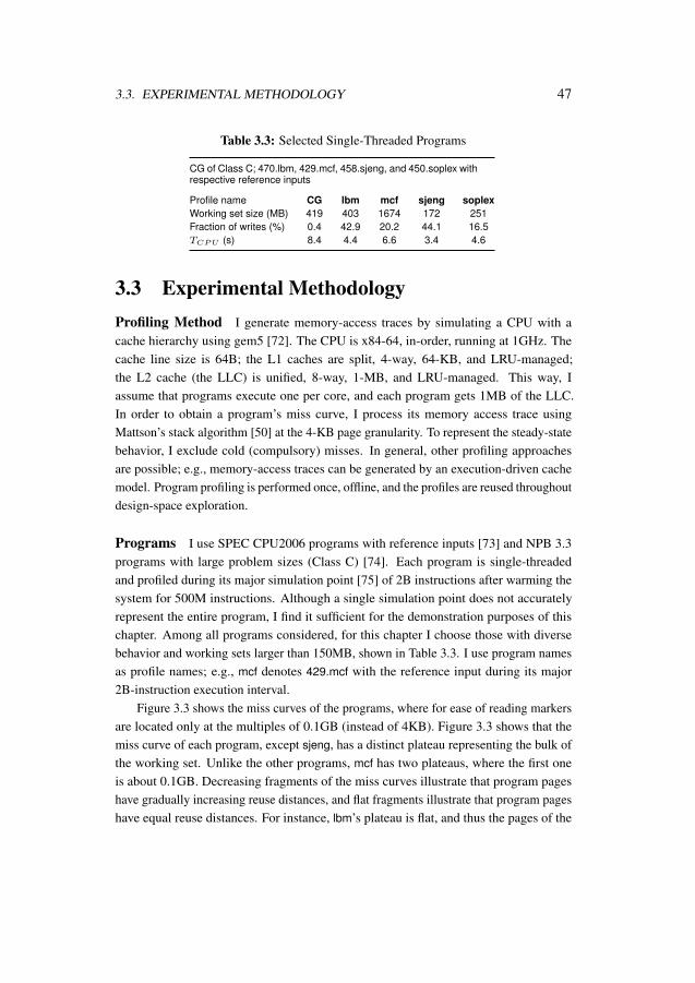
3.3. EXPERIMENTAL METHODOLOGY 47
Table 3.3: Selected Single-Threaded Programs
CG of Class C; 470.lbm, 429.mcf, 458.sjeng, and 450.soplex withrespective reference inputs
Profile name CG lbm mcf sjeng soplexWorking set size (MB) 419 403 1674 172 251Fraction of writes (%) 0.4 42.9 20.2 44.1 16.5TCPU (s) 8.4 4.4 6.6 3.4 4.6
3.3 Experimental MethodologyProfiling Method I generate memory-access traces by simulating a CPU with acache hierarchy using gem5 [72]. The CPU is x84-64, in-order, running at 1GHz. Thecache line size is 64B; the L1 caches are split, 4-way, 64-KB, and LRU-managed;the L2 cache (the LLC) is unified, 8-way, 1-MB, and LRU-managed. This way, Iassume that programs execute one per core, and each program gets 1MB of the LLC.In order to obtain a program’s miss curve, I process its memory access trace usingMattson’s stack algorithm [50] at the 4-KB page granularity. To represent the steady-statebehavior, I exclude cold (compulsory) misses. In general, other profiling approachesare possible; e.g., memory-access traces can be generated by an execution-driven cachemodel. Program profiling is performed once, offline, and the profiles are reused throughoutdesign-space exploration.
Programs I use SPEC CPU2006 programs with reference inputs [73] and NPB 3.3programs with large problem sizes (Class C) [74]. Each program is single-threadedand profiled during its major simulation point [75] of 2B instructions after warming thesystem for 500M instructions. Although a single simulation point does not accuratelyrepresent the entire program, I find it sufficient for the demonstration purposes of thischapter. Among all programs considered, for this chapter I choose those with diversebehavior and working sets larger than 150MB, shown in Table 3.3. I use program namesas profile names; e.g., mcf denotes 429.mcf with the reference input during its major2B-instruction execution interval.
Figure 3.3 shows the miss curves of the programs, where for ease of reading markersare located only at the multiples of 0.1GB (instead of 4KB). Figure 3.3 shows that themiss curve of each program, except sjeng, has a distinct plateau representing the bulk ofthe working set. Unlike the other programs, mcf has two plateaus, where the first oneis about 0.1GB. Decreasing fragments of the miss curves illustrate that program pageshave gradually increasing reuse distances, and flat fragments illustrate that program pageshave equal reuse distances. For instance, lbm’s plateau is flat, and thus the pages of the
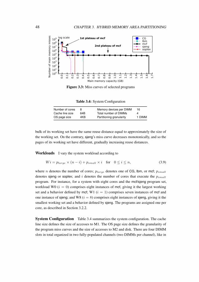
48 CHAPTER 3. HYBRID MEMORY AREA PARTITIONING
Figure 3.3: Miss curves of selected programs
Table 3.4: System Configuration
Number of cores 8 Memory devices per DIMM 16Cache line size 64B Total number of DIMMs 4OS page size 4KB Partitioning granularity 1 DIMM
bulk of its working set have the same reuse distance equal to approximately the size ofthe working set. On the contrary, sjeng’s miss curve decreases monotonically, and so thepages of its working set have different, gradually increasing reuse distances.
Workloads I vary the system workload according to
Wi = plarge × (n− i) + psmall × i for 0 ≤ i ≤ n, (3.9)
where n denotes the number of cores; plarge denotes one of CG, lbm, or mcf; psmalldenotes sjeng or soplex; and i denotes the number of cores that execute the psmallprogram. For instance, for a system with eight cores and the mcf/sjeng program set,workload W0 (i = 0) comprises eight instances of mcf, giving it the largest workingset and a behavior defined by mcf; W1 (i = 1) comprises seven instances of mcf andone instance of sjeng; and W8 (i = 8) comprises eight instances of sjeng, giving it thesmallest working set and a behavior defined by sjeng. The programs are assigned one percore, as described in Section 3.2.2.
System Configuration Table 3.4 summarizes the system configuration. The cacheline size defines the size of accesses to M1. The OS page size defines the granularity ofthe program miss curves and the size of accesses to M2 and disk. There are four DIMMslots in total organized in two fully-populated channels (two DIMMs per channel), like in

3.3. EXPERIMENTAL METHODOLOGY 49
Table 3.5: Default Parameter Values
DRAM revision G [76] Disk-cache hit rate 0%Non-memory power 50W Write-coalesce rate 0%Row-buffer hit rate 0% Overlap TCPU and Tmem NoBuffer disk writes No
Table 3.6: Characteristics of DRAM Revisions F and G
Numbers per rank of eight devicesAccess latencies exclude MC latencyRB = Row Buffer Revision F Revision G
RB miss RB hit RB miss RB hit
Latency (ns)64-B Read 35.00 18.75
Same as revision F64-B Write 61.25 18.75
Dynamic energy (nJ)64-B Read 40.49 11.24 20.77 6.1464-B Write 43.65 14.41 24.23 9.61
Power (mW)Static 840 540Refresh 32 21
Figure 3.2. Each DIMM has two ranks and eight memory devices per rank (for simplicity,no extra memory device for error detection and correction), and the organization is thesame for DRAM and NVM. I employ 128-MB DRAM devices [76], and so the capacityof a DRAM DIMM is 2GB, yielding 8GB of DRAM-only main memory capacity. Tomake some workloads not-in-memory w.r.t. the DRAM-only capacity, I scale it down fourtimes (to 2GB) by scaling the datasheet DRAM device capacity down to 32MB. I assumethat DRAM and NVM can be on the same channel and for demonstration purposes choosethe partitioning granularity of one DIMM6. Table 3.5 shows the default model parameters,where non-memory power is the system power excluding main memory and disk, andDRAM revision is explained below.
Memory Technologies DRAM and NVM DIMMs implement the 12.8GB/s DDR3interface. I derive the timing, power, and energy models for DRAM and NAND Flashfrom Micron’s datasheets [76, 77] and Power Calculator [78, 79]. I use the originaldatasheet numbers despite scaling the device capacities. I model both the latency andpower overheads of DRAM refresh and the erase-before-write overhead of NAND Flash.
The default DRAM revision is G [76], and for sensitivity analysis in Section 3.4.2I also model revision F [76], that has the same timing characteristics as revision G but atleast 1.5x worse electrical ones. Table 3.6 summarizes my estimates of selected numbers
6In real-world systems the partitioning granularity would be larger, e.g., one DIMM per channel.
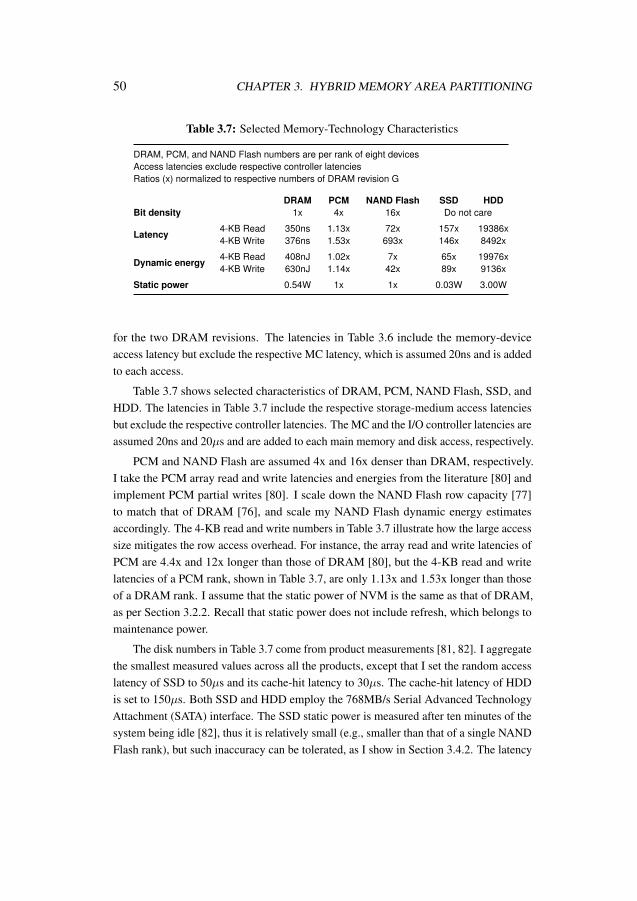
50 CHAPTER 3. HYBRID MEMORY AREA PARTITIONING
Table 3.7: Selected Memory-Technology Characteristics
DRAM, PCM, and NAND Flash numbers are per rank of eight devicesAccess latencies exclude respective controller latenciesRatios (x) normalized to respective numbers of DRAM revision G
DRAM PCM NAND Flash SSD HDDBit density 1x 4x 16x Do not care
Latency4-KB Read 350ns 1.13x 72x 157x 19386x4-KB Write 376ns 1.53x 693x 146x 8492x
Dynamic energy4-KB Read 408nJ 1.02x 7x 65x 19976x4-KB Write 630nJ 1.14x 42x 89x 9136x
Static power 0.54W 1x 1x 0.03W 3.00W
for the two DRAM revisions. The latencies in Table 3.6 include the memory-deviceaccess latency but exclude the respective MC latency, which is assumed 20ns and is addedto each access.
Table 3.7 shows selected characteristics of DRAM, PCM, NAND Flash, SSD, andHDD. The latencies in Table 3.7 include the respective storage-medium access latenciesbut exclude the respective controller latencies. The MC and the I/O controller latencies areassumed 20ns and 20µs and are added to each main memory and disk access, respectively.
PCM and NAND Flash are assumed 4x and 16x denser than DRAM, respectively.I take the PCM array read and write latencies and energies from the literature [80] andimplement PCM partial writes [80]. I scale down the NAND Flash row capacity [77]to match that of DRAM [76], and scale my NAND Flash dynamic energy estimatesaccordingly. The 4-KB read and write numbers in Table 3.7 illustrate how the large accesssize mitigates the row access overhead. For instance, the array read and write latencies ofPCM are 4.4x and 12x longer than those of DRAM [80], but the 4-KB read and writelatencies of a PCM rank, shown in Table 3.7, are only 1.13x and 1.53x longer than thoseof a DRAM rank. I assume that the static power of NVM is the same as that of DRAM,as per Section 3.2.2. Recall that static power does not include refresh, which belongs tomaintenance power.
The disk numbers in Table 3.7 come from product measurements [81, 82]. I aggregatethe smallest measured values across all the products, except that I set the random accesslatency of SSD to 50µs and its cache-hit latency to 30µs. The cache-hit latency of HDDis set to 150µs. Both SSD and HDD employ the 768MB/s Serial Advanced TechnologyAttachment (SATA) interface. The SSD static power is measured after ten minutes of thesystem being idle [82], thus it is relatively small (e.g., smaller than that of a single NANDFlash rank), but such inaccuracy can be tolerated, as I show in Section 3.4.2. The latency

3.4. EXPERIMENTAL RESULTS 51
Table 3.8: Hybrids and Respective Baselines
M1 M2 Disk DRA policya) DRAM b) PCM d) SSD f) LU
c) NAND Flash e) HDD g) HU
Label Hybrid Baseline Label Hybrid BaselineI-L a-b-e-f a-e-f III-L a-b-d-f a-d-f
I-H a-b-e-g a-e-g III-H a-b-d-g a-d-g
II-L a-c-e-f a-e-f IV-L a-c-d-f a-d-f
II-H a-c-e-g a-e-g IV-H a-c-d-g a-d-g
and dynamic energy of a 4-KB read from the disk cache respectively are 100x and 41xfor SSD, and 443x and 457x for HDD (normalized to those of a 4-KB read from a rankof DRAM revision G devices).
DRA Policies This chapter considers the LU and HU DRA policies. Both policiesstart with the initial allocation of 32MB of DRAM to each program. The remainingcapacity is distributed iteratively at a ∆c granularity of 1MB. The process stops if: 1) theentire memory capacity has been distributed among the programs, or 2) all programshave become in-memory w.r.t. the capacity allocated to them. At each iteration, onlynot-in-memory programs participate in allocation, and the LU and HU policies awardone ∆c to each program that has the lowest and the highest utility of it, respectively. Iftwo or more programs have the same utility of ∆c, each of them gets one ∆c, as long asthere is unallocated capacity. The policies first distribute the capacity of M1 and then thatof M2. Note that the DRA policies can be employed in DRAM-only systems, too.
Hybrid Organizations For comprehensive demonstration I consider eight hybridsystems, or hybrids for short, shown in Table 3.8. The baselines for the hybrids areDRAM-only systems with respective disk types and DRA policies.
3.4 Experimental Results
This section demonstrates Crystal by applying it to the hybrids from Table 3.8 and theworkloads from six program sets (mcf/sjeng, mcf/soplex, lbm/sjeng, lbm/soplex, CG/sjeng,and CG/soplex). Section 3.4.1 first shows the applicability of Crystal by presentingselected experimental results sufficient to illustrate key observations. Then, Section 3.4.2presents the validation of the partitioning results produced by Crystal.

52 CHAPTER 3. HYBRID MEMORY AREA PARTITIONING
Figure 3.4: Results for hybrids with HDD and mcf/soplex workloads
3.4.1 Applicability of Crystal
I set the goal to partition main memory area between DRAM and NVM such that system-level execution time and energy are within 20% of their respective global minima andthe area of the NVM partition is minimized. Due to the first-order nature of the models Iregard speedups and energy savings below 1.5-2x as noise and dismiss them. Minimizingthe area of the NVM partition keeps system cost and lifetime closest to those of thebaseline, as motivated below. Replacing a DRAM DIMM with an NVM DIMM doesnot reduce main memory cost, since for one NVM DIMM to cost less than one DRAMDIMM, NVM must cost less per bit for at least as many times as it is denser than DRAM(which does not hold even for NAND Flash, which is 16x denser but only 10x lessexpensive per bit than DRAM). Since NVM such as PCM and NAND Flash sufferfrom lower write endurance than DRAM, the less NVM is employed, the better it is forsystem lifetime.
Figures 3.4 to 3.7 show selected partitioning results and the respective speedups andenergy savings. Figures 3.4 to 3.7 have the same format, where the horizontal axis showsworkloads W0-W8 composed from different program sets according to (3.9). The bottomvertical axis shows the best partitioning (i.e., partitioning that meets the above goal) as theratio of the NVM area over the total main memory area. The normalized NVM area rangesfrom 0 to 75%, since main memory comprises four DIMMs in total, where one DIMM isalways DRAM to implement a hybrid with two partitions. That is, the partitioning optionsare one to three NVM DIMMs plus the DRAM-only baseline. The best partitioning foundfor execution time as the target metric is shown by bars, and that for execution energy is
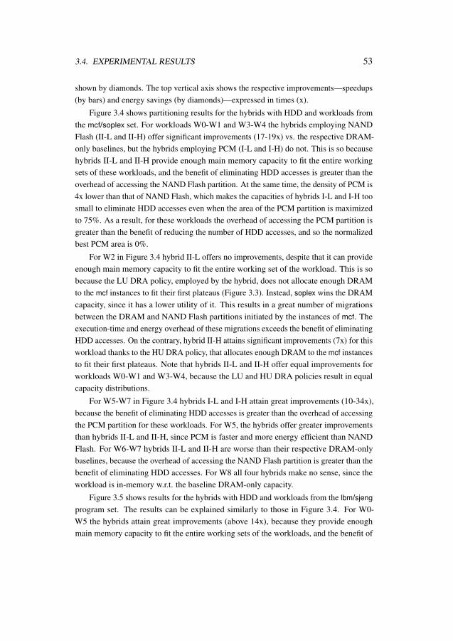
3.4. EXPERIMENTAL RESULTS 53
shown by diamonds. The top vertical axis shows the respective improvements—speedups(by bars) and energy savings (by diamonds)—expressed in times (x).
Figure 3.4 shows partitioning results for the hybrids with HDD and workloads fromthe mcf/soplex set. For workloads W0-W1 and W3-W4 the hybrids employing NANDFlash (II-L and II-H) offer significant improvements (17-19x) vs. the respective DRAM-only baselines, but the hybrids employing PCM (I-L and I-H) do not. This is so becausehybrids II-L and II-H provide enough main memory capacity to fit the entire workingsets of these workloads, and the benefit of eliminating HDD accesses is greater than theoverhead of accessing the NAND Flash partition. At the same time, the density of PCM is4x lower than that of NAND Flash, which makes the capacities of hybrids I-L and I-H toosmall to eliminate HDD accesses even when the area of the PCM partition is maximizedto 75%. As a result, for these workloads the overhead of accessing the PCM partition isgreater than the benefit of reducing the number of HDD accesses, and so the normalizedbest PCM area is 0%.
For W2 in Figure 3.4 hybrid II-L offers no improvements, despite that it can provideenough main memory capacity to fit the entire working set of the workload. This is sobecause the LU DRA policy, employed by the hybrid, does not allocate enough DRAMto the mcf instances to fit their first plateaus (Figure 3.3). Instead, soplex wins the DRAMcapacity, since it has a lower utility of it. This results in a great number of migrationsbetween the DRAM and NAND Flash partitions initiated by the instances of mcf. Theexecution-time and energy overhead of these migrations exceeds the benefit of eliminatingHDD accesses. On the contrary, hybrid II-H attains significant improvements (7x) for thisworkload thanks to the HU DRA policy, that allocates enough DRAM to the mcf instancesto fit their first plateaus. Note that hybrids II-L and II-H offer equal improvements forworkloads W0-W1 and W3-W4, because the LU and HU DRA policies result in equalcapacity distributions.
For W5-W7 in Figure 3.4 hybrids I-L and I-H attain great improvements (10-34x),because the benefit of eliminating HDD accesses is greater than the overhead of accessingthe PCM partition for these workloads. For W5, the hybrids offer greater improvementsthan hybrids II-L and II-H, since PCM is faster and more energy efficient than NANDFlash. For W6-W7 hybrids II-L and II-H are worse than their respective DRAM-onlybaselines, because the overhead of accessing the NAND Flash partition is greater than thebenefit of eliminating HDD accesses. For W8 all four hybrids make no sense, since theworkload is in-memory w.r.t. the baseline DRAM-only capacity.
Figure 3.5 shows results for the hybrids with HDD and workloads from the lbm/sjeng
program set. The results can be explained similarly to those in Figure 3.4. For W0-W5 the hybrids attain great improvements (above 14x), because they provide enoughmain memory capacity to fit the entire working sets of the workloads, and the benefit of

54 CHAPTER 3. HYBRID MEMORY AREA PARTITIONING
Figure 3.5: Results for hybrids with HDD and lbm/sjeng workloads
Figure 3.6: Results for hybrids III-L and III-H and lbm/sjeng workloads
eliminating HDD accesses is greater than the overhead of accessing the NVM partition.Hybrids I-L and I-H offer greater improvements for these workloads than hybrids II-Land II-H, since PCM is faster and more energy efficient than NAND Flash. For W6-W8all four hybrids are worse than their respective baselines, since these workloads arein-memory w.r.t. the baseline DRAM-only capacity.
As for the systems with SSD backing store, I find that for the workloads containingmcf, hybrids with PCM (III-L and III-H) provide either no benefit or not enough benefit forthe partitioning goal set in the beginning of this section. At the same time, hybrids IV-Land IV-H are never better than their respective baselines for all workloads considered,because the access latencies and dynamic energies of NAND Flash are too close to those

3.4. EXPERIMENTAL RESULTS 55
Figure 3.7: Results for hybrids with HDD and CG/sjeng workloads
of SSD, and the overhead of accessing the NAND Flash partition is greater than thebenefit of eliminating SSD accesses.
Figure 3.6 shows results for the hybrids with PCM, SSD, and workloads from thelbm/sjeng program set. The results resemble those for hybrids I-L and I-H in Figure 3.5:The improvements are significant for W0-W5 (4-8x) but smaller than those offered byhybrids I-L and I-H in Figure 3.5, since the access latency and dynamic energy gapsbetween DRAM and SSD are smaller than those between DRAM and HDD.
The results for workloads containing CG and respective workloads containing lbm
are similar, because CG and lbm have similar miss curves (recall Figure 3.3). For instance,compare Figure 3.7 and Figure 3.5: The best partitionings are the same, although CG
affects the improvements by having a much smaller fraction of writes and almost doubleTCPU compared to those of lbm (Table 3.3).
Intuitively, hybrid memory offers speedups and energy savings compared to equal-area DRAM-only memory if the benefit of reducing the number of disk accesses is greaterthan the overhead of migrations between the hybrid partitions. However, for specificworkloads speedups and energy savings can be relatively small (e.g., below 1.5x) andcan depend on DRA (e.g., the case of W2 in Figure 3.4). Crystal comes in handy in suchsituations and quickly identifies promising design points. For instance, Crystal showshow the density of NAND Flash enables hybrids that offer significant improvements forW0-W1 and W3-W4 in Figure 3.4, while the density of PCM is not high enough to offerany improvements for these workloads. The shorter access latencies and higher energyefficiency of PCM compared to NAND Flash bear no advantage is such cases.
56 CHAPTER 3. HYBRID MEMORY AREA PARTITIONING
Finally, I observe that for all the memory technologies, hybrids, and workloadsconsidered in this chapter, hybrid configurations that satisfy the partitioning goal minimizeexecution time at the same time as they minimizing execution energy, and speedups aresimilar to energy savings for each given hybrid and workload. In other words, executiontime and energy follow the same trend for the technologies. This is so because the NVMaccess latencies and dynamic energies are worse than those of DRAM but better thanthose of disk. Ultimately, partitioning can be done for execution time even if the actualtarget metric is energy, and this further simplifies the use of Crystal. In the next section Ivalidate the best partitionings identified by Crystal.
3.4.2 Validation of Partitionings Produced by Crystal
I validate the best partitionings produced by Crystal via sensitivity analysis, showingthat they are insensitive to the implementation-dependent details represented indirectly,as described in Section 3.2.2. I vary the model parameters in broad ranges coveringa large space of execution scenarios. Figure 3.8 shows the parameter values and theircombinations, 96 in total. In order to limit the number of combinations, Write-coalescerate is set to Row-buffer hit rate, assuming that writes that hit in the row buffer of M1 areguaranteed to not propagate to disk.
Each of the eight hybrids in Table 3.8 is partitioned for W0-W8 from each of the sixprogram sets (mcf/sjeng, mcf/soplex, lbm/sjeng, lbm/soplex, CG/sjeng, and CG/soplex)and each of the 96 parameter combinations. The results show that the best partitioning foreach given hybrid and workload is stable for all 96 combinations and the correspondingspeedups and energy savings vary understandably, as discussed below by the example ofthree selected hybrid/workload pairs.
Figures 3.9 to 3.11 show results for W4 from the lbm/sjeng set and hybrids II-L,I-L, and III-L, respectively. Figures 3.9 to 3.11 have the same format, as follows. Thehorizontal axis shows the parameter combinations from Figure 3.8. The vertical axis of thebottom graph shows the respective best partitionings as the NVM area normalized to thetotal main memory area. The vertical bars (of alternating shades for ease of reading) andthe diamonds show the best partitionings found for execution time and energy as the targetmetric, respectively. The vertical axis of the top graph shows the respective improvements:speedups (by vertical bars) and energy savings (by diamonds). The horizontal bars ofcolors from Figure 3.8 spanning across multiple parameter combinations annotate theparameter combinations of interest.
The improvements in Figures 3.9 to 3.11 are rather insensitive to the variation ofDRAM electrical characteristics represented by DRAM revisions F and G (Table 3.6).In addition, the results are rather insensitive to non-memory power, that I vary from
3.4. EXPERIMENTAL RESULTS 57
one-half to double the default value of 50W and observe insignificant changes in energysavings. This is why the inaccuracy of the SSD static power estimate in Section 3.3 istolerable. The robustness of the best partitioning (25% NVM in Figures 3.9 to 3.11)to such parameter value variations indicates that Crystal can be applied early in thedesign process, when accurate estimates of system component characteristics may not yetbe available.
The improvements offered by hybrid II-L in Figure 3.9 are most sensitive to row-buffer hit rate and disk-cache hit rate (see the parameter combinations below the lightblue and pink horizontal bars, respectively). The improvements vary as follows. Disk isnot accessed in the hybrid (the workload is in-memory w.r.t. its capacity), so disk-writebuffering and disk-cache hits do not affect its execution time and energy. Migrationsbetween the DRAM and NAND Flash partitions dwarf TCPU and DRAM accesses, thusthe execution time and energy are insensitive to the overlap of TCPU and Tmem and toDRAM row-buffer hits. At the same time, in the baseline system, disk accesses dwarfTCPU and DRAM accesses, so its execution time and energy are insensitive to the overlapof TCPU and Tmem, DRAM row-buffer hits, and disk-write buffering. However, the 99%row-buffer hit rate yields the 99% write-coalesce rate, that reduces the number of diskwrites and thus reduces the baseline execution time and energy. Likewise, disk-cachehits reduce the metrics. Thus, the high row-buffer and disk-cache hit rates result in lowerimprovements: They reduce the execution time and energy of the baseline system but donot affect those of hybrid II-L.
The improvements attainable by hybrid I-L in Figure 3.10 are sensitive to row-bufferand disk-cache hit rates, too, plus to the overlap of TCPU and Tmem (see the parametercombinations below the yellow bars). The sensitivity of the baseline execution timeand energy is the same as above, since hybrids II-L and I-L share the same baseline.Like in hybrid II-L, disk is not accessed in hybrid I-L, and so disk-write buffering anddisk-cache hits do not affect its execution time and energy. But unlike hybrid II-L, hybridI-L employs PCM, that is much faster and more energy efficient than NAND Flash. Asa result, migrations between the DRAM and PCM partitions do not dwarf TCPU andDRAM accesses, and so both the overlap of TCPU and Tmem and DRAM row-bufferhits reduce the execution time and energy of hybrid I-L. Thus, the overlap of TCPU andTmem results in higher improvements: It reduces the execution time and energy of thehybrid, but does not affect those of the baseline system. The 99% row-buffer hit rateincreases improvements, too: It reduces the execution time and energy of the hybridrelatively more compared to how the corresponding 99% write-coalesce rate reducesthose of the baseline.
The improvements offered by hybrid III-L in Figure 3.11 are sensitive to the sameparameters as described above for hybrid I-L, plus to disk-write buffering (see the

58 CHAPTER 3. HYBRID MEMORY AREA PARTITIONING
Figu
re3.
8:C
olor
codi
ngfo
rpar
amet
erva
lues
and
thei
rcom
bina
tions
Figu
re3.
9:Se
nsiti
vity
resu
ltsfo
rhyb
rid
II-L
and
W4
from
lbm
/sje
ngpr
ogra
mse
t

3.4. EXPERIMENTAL RESULTS 59
Figu
re3.
10:S
ensi
tivity
resu
ltsfo
rhyb
rid
I-L
and
W4
from
lbm
/sje
ngpr
ogra
mse
t
Figu
re3.
11:S
ensi
tivity
resu
ltsfo
rhyb
rid
III-
Lan
dW
4fr
omlb
m/s
jeng
prog
ram
set
60 CHAPTER 3. HYBRID MEMORY AREA PARTITIONING
parameter combinations below the red bars). Unlike the baseline for hybrid I-L, thebaseline for hybrid III-L employs SSD, which is much faster and more energy efficientthan HDD. As a result, SSD accesses do not dwarf TCPU and DRAM accesses, anddisk-write buffering reduces the execution time and energy of the baseline. On thecontrary, the parameter does not affect those of hybrid III-L, because the workload is in-memory w.r.t. its capacity and disk is not accessed. Thus, disk-write buffering decreasesimprovements. However, the 99% row-buffer hit rate diminishes the effect of buffering,since the corresponding 99% write-coalesce rate significantly reduces the number of diskwrites in the baseline.
The sensitivity analysis shows that the assumed model parameters do not affect thebest partitioning even if varied in broad ranges (though, they do affect speedups andenergy savings within understandable margins). Intuitively, each disk access and eachmigration between the DRAM and NVM partitions dwarf many execution details at higherlevels in the system. The best NVM areas for each hybrid and workload are stable amongall 96 parameter combinations. I find that this holds both at the partitioning granularity ofone DIMM and at a hypothetical, two times finer granularity. Thus, the first-order natureof the models employed by Crystal does not restrict its applicability.
3.5 Related Work
The problem of hybrid main memory design has both design- and run-time aspects. Run-time memory management dynamically distributes available memory capacity among co-running programs and performs dynamic data placement. Here I address the underlying,fundamental problem: design-time main memory area partitioning.
Qureshi et al. [15] replace all DRAM devices with PCM and add a DRAM cache tocreate a hierarchical hybrid system. The DRAM cache constitutes an area overhead. Mainmemory is backed by HDD with a NAND Flash cache. Using a detailed simulator, theauthors model candidate configurations for workloads that are not-in-memory w.r.t. theirDRAM-only baseline. Crystal can be modified to partition such hybrid memory organiza-tions and applied for evaluating more configurations with less computational effort.
Ekman and Stenstrom [30, 68] reduce main memory cost by replacing part of its fastDRAM with a less expensive, slower technology, and organizing hierarchical, migratingsystems. They study in-memory workloads with a detailed simulator identifying thecapacity of fast DRAM required for maintaining execution times similar to those ofthe baseline system. Such partitioning can be done with Crystal by setting the goalto: “for a fixed main memory capacity, minimize DRAM within a given degradation ofexecution time”.
3.6. SUMMARY 61
Ye et al. [69] consider in-memory workloads and NVM with a broad range ofaccess characteristics. Like Ekman and Stenstrom [30, 68], they set a goal to find ahybrid configuration with acceptable performance degradation while partitioning capacity(i.e., when the total capacity is fixed). They prototype hybrid memory on a real, DRAM-only machine via virtualization. The total capacity is limited to that of the host machine,and Crystal avoids this constraint.
Jacob et al. [83] propose an analytic, first-order model for finding the number andcapacities of levels in an n-level, replicating memory hierarchy for a given cost. UnlikeCrystal, the authors assume equal bit densities of memory technologies, treat all accessesas reads, and roughly approximate program miss curves abstracting away plateaus, thatare crucial for partitioning (recall the example in Section 3.2.1).
Yavits et al. [84] partition cache hierarchies of 3D chip multi-processors. Theypropose an analytic model for finding the optimal number and areas of cache levelsfor given area and power budgets. Unlike Crystal, the authors do not consider memorytechnologies with different bit densities and specialize their model to on-chip caches.
Choi et al. [85] partition hybrid memories that are flat (both the DRAM and NVMpartitions can be accessed directly). They propose a model for finding the optimalplacement of in-memory program data that minimizes execution energy, time, theirproduct, or the number of writes to the NVM partition, and evaluate hybrid configurationsof the same total capacity. The model neither includes disk nor considers main memoryarea. It employs integer linear programming and thus implies a limit on the working-setsize for which the optimal data placement can be practically found. On the contrary,Crystal is holistic (models the entire system and is thus applicable for both in-memoryand not-in-memory workloads) and practical (considers memory area and is applicablefor workloads with realistic working-set sizes).
3.6 Summary
The right balance between DRAM and NVM is fundamental for hybrid main memorydesign, but detailed simulation or prototyping alone impede comprehensive design-spacesearch required for finding it. I propose Crystal, an analytic approach to the design-timeresource partitioning of hierarchical hybrid systems. Crystal is holistic and enables earlypartitioning, thus facilitating exhaustive design-space exploration. It employs system-level models providing first-order estimates of execution time and energy. The bestpartitionings identified by Crystal are validated via sensitivity analysis, showing that theyare robust to the imprecision of the models.

62 CHAPTER 3. HYBRID MEMORY AREA PARTITIONING
Crystal quickly identifies the best amount and type of NVM given a partitioning goaland a workload, highlighting the most promising design points for subsequent detailedevaluation. For instance, Crystal shows how higher system-level performance and energyefficiency can be achieved by employing an NVM with the speed and energy consumptionof NAND Flash instead of a faster and more energy efficient NVM like PCM.
However, Crystal explores only a subset of the design space. In the next chapter, Ipresent a generalized framework named Rock. Unlike Crystal, Rock mutually considerstotal main memory area, its partitioning, capacity allocation among programs, and dataplacement within allocated capacities, among other design dimensions. This way, Rockallows system architects to obtain insights about the entire design space to prune it.

4Pruning of Hybrid Memory
Design Space
The problem sizes of contemporary workloads continuously grow and thereby drive thedemand for larger and still fast main memory. System architects can address this demandby: 1) installing more memory modules and/or 2) using modules of larger capacities.SCM technologies like PCM promise significantly higher densities than DRAM and lowercosts per bit. Thus, combining DRAM and SCM modules allows system architects tobuild hybrid main memories that are more cost-effective than DRAM-only memories [8].
Memory system performance in case of DRAM-only memory depends on manyfactors like: 1) the workload, 2) the total number of memory-module slots, 3) the type ofDRAM modules, 4) DRAM capacity allocation among co-running programs, and 5) disktype, to name a few. In case of hybrid main memory, new factors are added, e.g.: 6) thenumber and type of SCM modules, 7) SCM capacity allocation, and 8) data placementwithin the DRAM and SCM capacities allocated per program. Thus, the design space ofhybrid main memory systems is multi-dimensional.
63

64 CHAPTER 4. HYBRID MEMORY DESIGN-SPACE PRUNING
The design point with the highest performance can be found via Design-SpaceExploration (DSE). Complete and accurate DSE where each design point is evaluatedonly via prototyping [69, 86–90] and/or simulation [15, 24, 25, 30, 68, 91, 92] isproblematic due to high implementation and/or computation efforts, respectively. Analyticmodeling [34, 85] is much quicker than simulation, but is less accurate due to its first-order nature. Thus, it is most appropriate for inferring trends and validating them viasensitivity analysis. Crystal [34], presented in the previous chapter, employs analyticmodels to partition a fixed number of memory-module slots between DRAM and SCM.However, it explores only a subspace of the design space considered in this chapter, since:1) it does not compare memory systems comprising different total numbers of memorymodules, and 2) it employs a single policy for data placement, thus disregarding it as adesign dimension.
This chapter proposes Rock, a generalized framework for pruning the design spaceof hybrid main memory systems. A novelty of Rock is that it recognizes and mutuallyconsiders such important design dimensions as: 1) total memory-system area, 2) memory-system area partitioning between DRAM and SCM, 3) allocation of the DRAM and SCMcapacities among co-running programs, and 4) data placement within the allocated ca-pacities. Design-space trends inferred during first-order DSE are validated via sensitivityanalysis; trends that pass validation are used for design-space pruning.
The first contribution of this chapter is that it systematizes hybrid memory designdimensions by distinguishing area partitioning, resource allocation, and data placement.The second contribution is a framework that helps system architects to quickly inferimportant design-space trends by mutually considering the above dimensions, among theconventional ones. For instance, Rock makes it easy to reveal insensitivity to a specificdesign dimension in the context of the other dimensions, significantly simplifying thedesign space. This chapter demonstrates the power of Rock by applying it to two carefullyselected example workloads and a scaled memory system with up to six DRAM and/orPCM modules backed by NAND Flash SSD. Using Rock I reduce the number of designpoints to just a few.
The rest of the chapter is organized as follows. Section 4.1 explains hybrid memorydesign dimensions, Section 4.2 presents Rock, Section 4.3 the experimental methodology,and Section 4.4 results. Finally, Section 4.5 discusses related work and Section 4.6summarizes the chapter.

4.1. HYBRID MEMORY DESIGN DIMENSIONS 65
Figure 4.1: Proposed system of design dimensions
4.1 Hybrid Memory Design Dimensions
The design space of hybrid memory systems is multi-dimensional. Among the otherdimensions like the type of DRAM and SCM, I propose to recognize: 1) resourcepartitioning, i.e., the decision of how much memory of each type to use; 2) resourceallocation, i.e., the distribution of DRAM and SCM capacities among co-runningprograms; and 3) data placement, i.e., the decision of where within the allocated capacitiesto store each program’s data.
In this chapter, I assume that resource partitioning is performed at design-time, andthus it poses the question of how many DRAM and SCM modules to install, given thatthe total number of modules is fixed. I do not consider run-time resource partitioningenabled by the dynamic reconfiguration of SCM cells [93]. Resource allocation and dataplacement can be performed both at design- and run-time. I propose to systematize thedesign dimensions as shown in Figure 4.1, where the arrows show possible dependencies.For instance, design-time resource partitioning defines the capacities for either design- orrun-time resource allocation. The proposed systematization facilitates directing DSE.
Resource allocation controls how much of the total DRAM and SCM capacities isavailable to each program. If a program is allocated enough capacity to hold its entireworking set, it becomes in-memory and does not access disk in the steady state, whichis a key to high performance. In general, resource allocation that results in the highestperformance is an NP-complete problem even in conventional, one-level memories suchas shared caches [71] or DRAM-only main memories [94]. One way to implementresource allocation is to drive allocation decisions by utility, where a program’s utility ofa specific capacity slice is defined as the number of main memory capacity misses thatcan be eliminated by allocating the slice to the program.

66 CHAPTER 4. HYBRID MEMORY DESIGN-SPACE PRUNING
Figure 4.2: System with flat hybrid main memory
In general, data placement that results in the highest performance is an NP-completeproblem, too [24, 25, 85, 91, 92, 95]. Data placement can be imposed by the organizationof hybrid memory partitions. For brevity, like in the previous chapter, I label the DRAMpartition M1 and the SCM partition M2. The hierarchical organization of M1 and M2,like in Figure 3.1b of the previous chapter, imposes a basic data placement policy, whereM2 can only be accessed via M1. Alternatively, the partitions can be organized as flathybrid memory, shown in Figure 4.2, where the CPU can directly access both M1 andM2, allowing flexibility for sophisticated data placement policies.
Another possible dimension is the policy for promoting data (from M2 to M1):migrating hybrid memories move data upon promotion, while replicating memories copy.Since this thesis strives to maximize main-memory capacity, I consider migrating hybridmemories throughout.
As already mentioned, the design point with the highest performance can be foundusing DSE. However, complete and accurate DSE solely via prototyping and/or simulationis problematic due to high costs, restrictions and/or inefficiencies. The next sectionpresents Rock, a framework for pruning hybrid memory design spaces and therebyfacilitating complete and accurate DSE.
4.2 RockRock employs analytic models to quickly prune design spaces of hybrid main memorysystems. Analytic models have limited accuracy but make it possible to quickly infertrends specific to a design space by comparing relative performance of its design points.Rock normalizes the performance of each design point to that of the reference one: thedesign point with the highest performance, i.e., the DRAM-only system with capacitylarge enough for the workload to be in-memory. Normalization removes effects commonto the design points, equivalently making such common effects unnecessary to model.The inferred trends are then validated using systematic sensitivity analysis. For instance,two sets of parameters can be used per design point to represent corner-case scenarios: ascenario with low performance and a scenario with high performance. Other executionscenarios would yield performance falling in between the two corner cases. If a trend

4.2. ROCK 67
Table 4.1: DRA Policies
LU Low-Utility First allocates capacity to programs with low utility of itHU High-Utility First allocates capacity to programs with high utility of itUA Utility-Agnostic Allocates capacity regardless of utility
holds in both cases, I conclude that it is insensitive to the inaccuracies of analytic modelingand thus it can be used for design-space pruning.
For instance, in a simplified example, I can vary the average access-latency gapbetween DRAM and PCM by assuming a low row-buffer hit rate in one corner case and ahigh row-buffer hit rate in the other corner case. Then, if I observe in both corner cases atrend that, e.g., replacing DRAM with PCM improves performance (due to reducing thenumber of disk accesses), I can conclude that the trend is insensitive to the variation ofrow-buffer hit rate. Therefore, I can use this trend to prune the design space.
A novelty of Rock is that it mutually considers resource partitioning, resourceallocation, and data placement, among the other design dimensions. In this chapterRock extends Crystal [34] by integrating its method for workload representation (offlineprofiling) and the baseline first-order performance model. In addition, Rock integratesapproximations for different implementations of resource allocation and data placement.The rest of this section details Rock.
4.2.1 Workload Representation
Rock adopts Crystal’s [34] workload representation method, where each program isapproximated by a profile (Table 3.1) comprising: 1) the miss curve showing the numberof main-memory misses vs. capacity, and 2) the fraction of writes equal to the numberof main-memory write requests over the total number of main-memory requests. Iexclude from the profile the time spent on computation and cache accesses in order toemphasize the difference between main memory configurations. Such profiling is a one-time, offline effort (a profile is created once and reused throughout design-space pruning).I consider multiprogrammed workloads comprising one single-threaded program per core.A workload is represented by a set of respective program profiles.
4.2.2 Resource Allocation
I purpose to compare memory systems employing different DRA policies to reveal thesensitivity (or lack thereof) of the memory-system performance to resource allocation.I perform resource allocation at design-time (statically) using three distinct policies

68 CHAPTER 4. HYBRID MEMORY DESIGN-SPACE PRUNING
shown in Table 4.1: the LU and HU policies introduced in the previous chapter and aUtility-Agnostic (UA) policy, that awards capacity to programs regardless of their utilityof it. To further investigate the sensitivity of the memory-system performance to resourceallocation, other polices can be integrated into the framework of Rock.
4.2.3 Data PlacementFor simplicity of demonstration, I manage program data at the OS page granularity forboth paging to/from disk and migrations between M1 and M2 (though other granularitiescan be considered). First-order performance estimates for the conventional system(Figure 3.1a) and the hierarchical hybrid system (Figure 3.1b) can be obtained using themodel that captures the basic memory-system behavior, presented in Section 3.2.3 of theprevious chapter. Like in the previous chapter, main memory is assumed fully-associativeand implements the LRU replacement policy1.
Like in the previous chapter, I consider the following steady-state behavior. If arequested page is not present in memory, it is paged-in from disk to main memory of theconventional system or to M2 of the hierarchical hybrid system. Each page-in causes apage-out, but only dirty pages are written back to disk. If a requested page is not presentin M1 but is present in M2, it is moved from M2 to M1 (since the memory is migrating).Each migration from M2 to M1 causes a migration from M1 to M2. This behavior imposesa Run-time Data Placement (RDP) policy labeled basic. The total memory-access time ofa single-threaded program running in a hybrid system that employs this RDP policy canthus be estimated by (3.1). In order to emphasize the difference among main memoryconfigurations, I exclude from (3.1) the time spent on computation and all cache accesses(TCPU ) to obtain the following model:
T = NM1· ((1− fWr)· tM1Rd + fWr· tM1Wr)
+NM2· (tM2→M1 + tM1→M2) (4.1)
+ND· (tD→M2 + (1− wcr)· fWr· tM2→D),
where the parameters and variables are described in Table 4.2 and computed the sameway as in Section 3.2.3.
The equation for the total memory-access time of a single-threaded program in thesystem with one-level main memory (Figure 3.1a) can be obtained from (4.1) by excludingM2, and I omit it for brevity. I consider design points where the entire main memory can
1An important nuance of migrating hybrid memories where address mappings between M1 andM2 are restricted [26–28] is that resource allocation can be controlled by data placement. Integratingmodels for such systems into Rock can be a future-work direction.

4.2. ROCK 69
Table 4.2: Parameters and Variables in (4.1)
NM1, NM2, ND The numbers of accesses to M1, M2, and disk, respectively
fWr The program’s fraction of writes
tM1Rd, tM1Wr Respective latencies of reading and writing one cache line from/to M1
tM2→M1, tM1→M2 Respective latencies of one page migration from M2 to M1 and from M1 to M2
wcr An assumed write-coalesce rate, i.e., the fraction of all writes to main memorythat do not propagate to disk
tD→M2, tM2→D Respective latencies of one page-in from disk to M2 and one page-out fromM2 to disk
be either DRAM or SCM, too, and so in the context of one-level main memory M1 candenote either DRAM or SCM. For simplicity of modeling, I assume that DRAM andSCM modules have the same organization.
Like in Crystal, the assumed model parameters can indirectly represent system-behavior nuances as follows: 1) Row-buffer hit rate (rbhr) allows us to vary the latencyper M1 access and loosely represents execution details like access reordering and differentforms of parallelism (e.g., bank-level). Since in the hierarchical hybrid system M2 isaccessed only at the page granularity, a separate model parameter is unnecessary; 2) Write-coalesce rate (wcr) allows us to vary the number of page writebacks to disk and representswrites coalescing with other writes within a page before it is paged-out; and 3) Disk-cachehit rate (dchr) allows us to vary the latency per disk read and represents prefetching tothe disk cache that typically benefits only reads [51].
Next, to model the flat hybrid system of Figure 4.2, I propose to augment (4.1) withtwo hypothetical RDP policies. The first one is labeled “80%” and eliminates 80% ofmigrations between M1 and M2, i.e., N ′M2 = 0.2·NM2, where NM2 corresponds to thebasic RDP policy. The second RDP policy is labeled ideal and eliminates all migrations,i.e., it represents the system of Figure 3.1a where main memory is built from DRAM buthas the aggregate capacity of M1 and M2. The two policies are simple yet effective forobtaining important insights, as I will demonstrate in Section 4.4. Other RDP policiescan be integrated into the framework of Rock.
4.2.4 Final Calculations
The total memory-access times of all programs are summed to obtain the total memory-access time of the workload. Next, I add the periodic maintenance overhead of DRAM(refresh), except for SCM-only systems. I assume that refresh overlaps for all DRAM
70 CHAPTER 4. HYBRID MEMORY DESIGN-SPACE PRUNING
modules, and therefore calculate its overhead as the total memory-access time multipliedby the refresh latency and divided by the refresh period.
Finally, I estimate memory system performance by its throughput, given by the totalnumber of main-memory requests multiplied by the request size (i.e., cache line size) anddivided by the total memory-access time (i.e., main-memory plus disk access time). As Iexplain in the first paragraph of this section, for the estimates for each design point to beuseful they have to be normalized to the reference design point (the DRAM-only systemin which the workload is in-memory).
Note that in addition to the performance model, an analytic energy model like (3.2)and (3.6) to (3.8), employed by Crystal, can be straightforwardly integrated into theframework of Rock for pruning design spaces where the target metric is energy. Aninteresting question is to test whether the observation that for the current state of memorytechnologies energy follows the same trends as performance [34] holds for the largerdesign spaces considered by Rock.
4.3 Experimental MethodologyThe purpose of the evaluation of Rock in this chapter is to demonstrate its power in termsof quick and accurate design-space pruning to select the most promising design points fordetailed evaluation via prototyping and/or simulation.
Programs and Workloads Rock uses the same programs and the profiling methodas Crystal (Section 3.3). I carefully choose two distinct example workloads labeled Work1and Work2 (Table 4.3). Work1 comprises multiple instances of the same program (sjeng),and so it is insensitive (in terms of performance) to different implementations of resourceallocation. In other words, the UA, LU, and HU DRA polices (Table 4.1) produce equalmemory-capacity allocations for Work1. In addition, unlike the other programs, sjeng
has a miss curve without plateaus, i.e., its miss curve decreases gradually (Figure 3.3).Thus, sjeng benefits from more capacity as long as it is not-in-memory. Work2 comprisesdifferent programs (CG, lbm, mcf, and soplex), and so its performance can be sensitiveto different resource-allocation policies (due to different M1-capacity allocations perprogram). That is, Work2 creates a larger design space than Work1. In addition, the misscurves of its programs have plateaus and cliffs (steep drops). For instance, Figure 3.3shows that mcf’s total number of misses is ∼2· 108, that drops down to ∼107 at 0.05GBand down to ∼105 at 0.1GB. The next section illustrates the importance of such plateausand cliffs for hybrid memory system performance. The aggregate working set size ofWork1 is 16×172 = 2752MB and that of Work2 is 419+403+1674+251 = 2747MB.

4.3. EXPERIMENTAL METHODOLOGY 71
Table 4.3: Selected Workloads
Work1 16 instances of sjengWork2 One each of CG, lbm, mcf, soplex
Table 4.4: System Configuration
Number of cores 16 (Work1), 4 (Work2)Cache line size 64BOS page size 4KBMax number of DIMMs 6Partitioning granularity 1 DIMM
Resource Allocation I consider the UA, LU, and HU DRA policies (Table 4.1). Theinitial allocation is 32MB for each program, and ∆c is 1MB.
System Configuration I execute Work1 in a 16-core system and Work2 in a 4-coresystem (one program per core). Main memory is organized as channels populated withDIMMs. For demonstration purposes I scale down the memory size and choose oneDIMM as the unit by which the memory size can be changed2. I assume that DRAM andSCM can share the same channel and that the partitioning granularity, i.e., the unit bywhich DRAM can be replaced with SCM, is one DIMM.
The maximum number of DIMMs is chosen such that the workloads are in-memoryw.r.t. the DRAM-only capacity. Each DIMM has two ranks and eight memory devicesper rank (for simplicity, no extra memory device for error detection and correction), andthe organization is the same for DRAM and SCM. I employ 1-Gb DRAM devices [76]and scale down their capacity four times, resulting in 512-MB DRAM DIMMs. Thus, tomatch the working set sizes of Work1 and Work2, I need six DRAM DIMMs (3072MBin total). The DRAM-only system of six DIMMs is therefore the reference design point,whose performance should ideally be matched by hybrid systems with fewer modules.Table 4.4 summarizes the system configuration.
Memory Technologies I consider systems employing DRAM, PCM, and NANDFlash SSD (though in general Rock is applicable to other technologies, too). PCM isassumed four times denser than DRAM [15]. DRAM and PCM DIMMs implement the12.8GB/s DDR3 interface, and I model the access latencies of DRAM and PCM according
2In real-world, large systems the unit would be one DIMM per channel or one rank of memorydevices per channel.

72 CHAPTER 4. HYBRID MEMORY DESIGN-SPACE PRUNING
Table 4.5: Memory-Technology Access Latencies
Access latencies exclude respective controller latenciesRatios (x) are normalized to respective DRAM latencies
64-B Read 64-B Write 4-KB Read 4-KB WriteDRAM 35ns 61.25ns 350ns 376nsPCM 2.26x 4.23x 1.13x 1.53xSSD Not used Not used 157x 146x
Table 4.6: Sets of Assumed Parameter Values for Sensitivity Analysis
Set1 Set2Row-buffer hit rate (%) 0 99Write-coalesce rate (%) 0 99Disk-cache hit rate (%) 0 50
to a datasheet [76] and the literature [80]. SSD employs the 768MB/s SATA interfaceand has a random access latency of 50µs. Table 4.5 summarizes “raw” DRAM, PCM,and SSD access latencies, that include the respective storage-medium access latencies butexclude the respective controller latencies.
The latency of a 64-B access hitting in the row buffer of DRAM or PCM is 18.75ns.The latency of a 4-KB read hitting in the SSD cache is 30µs. The MC and the I/Ocontroller latencies are assumed 20ns and 20µs, respectively, and are added to eachmain-memory and disk access. The latency and period of DRAM refresh are 110ns and7.8125µs, respectively [76].
Sensitivity-Analysis Parameters I perform sensitivity analysis by varying theassumed model parameters (Section 4.2.3) in broad ranges, shown in Table 4.6. Foreach design point, Set1 represents a corner case where the total memory-access time isthe longest, and Set2 represents that where the total memory-access time is significantlyshorter. Other execution scenarios would result in total memory-access times falling inbetween the two corner cases. Thus, if a design-space trend holds in both corner cases,I conclude that it is insensitive to the inaccuracies of first-order modeling. Note thatreal-world cases might require more than two sets for comprehensive sensitivity analysisto narrow down the ranges of parameter values for which the trends of interest hold.
4.4. EXPERIMENTAL RESULTS 73
4.4 Experimental Results
This section demonstrates that Rock can prune design spaces effectively. Sections 4.4.1and 4.4.2 present results for the design spaces created by Work1 and Work2, respectively.
4.4.1 Work1 Design-Space Pruning
I consider only the UA DRA policy for Work1, since the workload is insensitive todifferent resource-allocation policies, as explained in Section 4.3. Figure 4.3 shows a3D view of the design space for parameter values Set1 (Table 4.6) and has the followingformat. The X axis shows the total number of DIMMs, ranging from one to six. The Yaxis shows the number of PCM DIMMs (out of the total number of DIMMs), ranging fromzero to six. I use the (X,Y ) notation throughout this section to denote different memoryconfigurations. For instance, (2, 0) denotes DRAM-only memory of two DIMMs, (2, 1)
denotes hybrid memory of one DRAM and one PCM DIMMs, (2, 2) denotes PCM-onlymemory of two DIMMs, and {(x, y) | x ∈ [2, 3] ∧ y ∈ [1, x− 1]} denotes hybrid memoriesof two and three DIMMs ((2, 1), (3, 1), and (3, 2)). The Z axis shows the memory-systemthroughput normalized to that of the (6, 0) system (the reference). The surface shows thenormalized throughput of the systems employing the basic RDP policy. The ribs of thesurface are projected onto the XZ plane as contour plots. For instance, the normalizedthroughput of the {(x, x) | x ∈ [2, 6]} systems is about 0.38. The error bars with circles andthe error bars with dashes show the normalized throughput of the systems employing the“80%” RDP policy and the ideal RDP policy, respectively. For instance, the throughput ofthe (6, 5) system is about 0.3 if it employs the “80%” RDP policy and 1.0 if it employsthe ideal RDP policy.
Figure 4.4a shows the same design space but in a two-dimensional view (for theease of quantitative analysis) and has the following format. The horizontal axis showsthe total number of DIMMs. Each group of bars shows configurations of the same totalnumber of DIMMs, where the left-most and the right-most bars correspond to the DRAM-only and the PCM-only configurations, respectively. The vertical axis shows throughputnormalized to the (6, 0) system. Figure 4.4b has the same format as Figure 4.4a andshows results for parameter values Set2 (Table 4.6), used for sensitivity analysis. Next,I discuss how I infer trends by analyzing the resource-partitioning results first and thenthe data-placement results (recall the dependency between resource partitioning and dataplacement in Figure 4.1).

74 CHAPTER 4. HYBRID MEMORY DESIGN-SPACE PRUNING
Figure 4.3: Design space of Work1 with UA DRA policy and Set1 in 3D view
Resource Partitioning
Figures 4.3 and 4.4a show that the throughput of the {(x, 0) | x ∈ [1, 5]} systems isvery low, under 10% of the reference throughput (the (6, 0) system). Thus, I inferthat the performance of the {(x, 0) | x ∈ [1, 5]} systems is disk-bound. This trend holds inFigure 4.4b, too, and so it is insensitive to the errors of analytic modeling and thus canbe used for design-space pruning. That is, I can dismiss the {(x, 0) | x ∈ [1, 5]} systems,since they offer low performance due to disk accesses.
Intuitively, I can improve performance by replacing some DRAM with PCM andthus provisioning more capacity. I first analyze the resource-partitioning results forhybrid systems {(x, y) | x ∈ [2, 6] ∧ y ∈ [1, x− 1]} and then those for PCM-only systems{(x, x) | x ∈ [1, 6]}. In order to focus on resource partitioning, I first consider only thesystems employing the basic RDP policy.
Figures 4.3 and 4.4a show that the {(x, 1) | x ∈ [2, 5]} systems outperform the re-spective {(x, 0) | x ∈ [2, 5]} systems. For instance, the normalized throughput of the(4, 1) system is about 0.3, but that of the (4, 0) system is under 0.025. Thus, in the{(x, 1) | x ∈ [2, 5]} systems the benefit of a larger capacity exceeds the overhead ofmigrations between M1 and M2. Therefore, I infer that performance can be improvedby replacing one DIMM of the {(x, 0) | x ∈ [2, 5]} systems with PCM. This holds inFigure 4.4b, too, and so the trend can be used for pruning.

4.4. EXPERIMENTAL RESULTS 75
(a) Set1
1 2 3 4 5 6Total number of DIMMs
0.0
0.2
0.4
0.6
0.8
1.0
Norm
. th
roughput
(b) Set2 (sensitivity analysis)
Figure 4.4: Design space of Work1 with UA DRA policy in two-dimensional view
Next, Figures 4.3 and 4.4a show that the {(x, 1) | x ∈ [3, 6]} systems outperform the{(x, y) | x ∈ [3, 6] ∧ y ∈ [2, x− 1]} systems, where each system employs the basic RDPpolicy. For instance, the normalized throughput of the (3, 1) system is about 0.19, but thatof the (3, 2) system is less than 0.1. Intuitively, replacing more DRAM with PCM doesnot add useful capacity for Work1, but it increases the overhead of migrations betweenM1 and M2. Thus, I infer that employing two or more (but not all) PCM DIMMs reducesperformance, compared to that of the respective systems with just one PCM DIMM. Thistrend holds in Figure 4.4b, too, and thus I can use it for design-space pruning.
Finally, Figures 4.3 and 4.4a show that PCM-only systems {(x, x) | x ∈ [1, 5]} outper-form the respective DRAM-only systems {(x, 0) | x ∈ [1, 5]}. Although the performance

76 CHAPTER 4. HYBRID MEMORY DESIGN-SPACE PRUNING
of the (1, 1) system is still disk-bound, the {(x, x) | x ∈ [2, 5]} systems attain a normalizedthroughput of about 0.38. On the contrary, even the (5, 0) system attains that of less than0.1. This means that in the PCM-only systems the benefit of a larger capacity exceedsthe penalty of accessing PCM directly. Thus, I infer that replacing all DIMMs of the{(x, 0) | x ∈ [2, 5]} systems with PCM can be an attractive option. This trend holds inFigure 4.4b, too. Moreover, thanks to the very high assumed row buffer hit rate in Set2,the {(x, x) | x ∈ [2, 6]} systems in Figure 4.4b are competitive with the (6, 0) system.Though, the PCM write-endurance issue must be alleviated before PCM-only systemscan be deployed [8]. Otherwise, the write traffic of Work1 (44.1% of all memory requests,according to Table 3.3) might wear out PCM faster than the desired system lifetime.Future SCM technologies with higher write endurance might become a feasible DRAMreplacement option, and Rock can help to identify such opportunities.
Data Placement
The ideal RDP policy is used to identify hybrid memory configurations that are disk-bound: in such systems, the ideal RDP policy cannot match the throughput of the (6, 0)
system. For instance, Figures 4.3 and 4.4a show that the normalized throughput of the(2, 1) system is less than 0.1 even if it employs the ideal RDP policy. Figure 4.4b supportsthis observation, and thus the (2, 1) system can be safely discarded.
Figures 4.3 and 4.4a show that the “80%” RDP policy significantly improves theperformance of the {(x, y) | x ∈ [3, 6] ∧ y ∈ [1, x− 1]} systems compared to the basicRDP policy. However, in the systems with just one DRAM DIMM ({(x, y) | x ∈[3, 6] ∧ y = x− 1}) the number of migrations between M1 and M2 is still large, boundingperformance to about 0.3. This means that sophisticated RDP policies, approximated bythe “80%” policy, have a high potential, but in systems with a large number of migrationsthey have to eliminate much more than 80% of migrations to be competitive with thereference (6, 0) system. This trend holds in Figure 4.4b, too.
Summary
The purpose of Rock is to help us infer and validate trends for pruning away unpromisingdesign points. The analysis above leaves us with hybrid systems of three to five DIMMsin total, of which one is PCM (the {(x, 1) | x ∈ [3, 5]} systems), employing a sophisticatedRDP policy. This way, I prune the design space in Figure 4.3 down to three design points(the above three hybrid systems) plus one (the (6, 0) reference system).
Note that the maximum total number of DIMMs is a restriction external to Rock inthis evaluation. When the total capacity is large enough to make the workload in-memory,systems with the ideal RDP policy are equivalent to the (6, 0) system and thus could be

4.4. EXPERIMENTAL RESULTS 77
excluded from the design space even without Rock, by just estimating the workload’saggregate working-set size. In addition, as long as the limited write endurance of PCMremains an issue, the PCM-only systems could be safely excluded for this workload.
4.4.2 Work2 Design-Space PruningSince Work2 might be sensitive to different implementations of resource allocation, Iconsider the UA, LU, and HU DRA policies (Table 4.1). Figures 4.5, 4.6, and 4.7 showthree-dimensional views of the respective design subspaces for parameter values Set1(Table 4.6). Figures 4.5, 4.6 and 4.7 have the same format as Figure 4.3 and show thatWork2 is very distinct from Work1. One striking difference is that there are hybridsystems in Figures 4.5 and 4.6 (i.e., (4, 1), (5, 1), (5, 2), and {(6, y) | y ∈ [1, 3]}) that attainnearly the same throughput as the reference (6, 0) system, regardless of the RDP policy.I explain the reason and implications of this when discussing the sensitivity to dataplacement later in this section.
For brevity, to discuss only new insights (compared to those I have discussed forWork1), I restrict my further analysis to the subspace formed by systems of two tofour DIMMs. Figures 4.8, 4.9, and 4.10 show the results for the {(2, y) | y ∈ [0, 2]},{(3, y) | y ∈ [0, 3]}, and {(4, y) | y ∈ [0, 4]} systems, respectively. The format of the left(Set1) and right (Set2) parts of the figures is the same as that of Figure 4.4a, exceptthat the horizontal axis now shows the DRA policy. To highlight new insights, I buildthe following discussion around performance sensitivity to resource allocation and dataplacement. In this chapter I consider design points with high sensitivity undesirable, andthus set a goal to prune them away.
Sensitivity to Resource Allocation
Figures 4.8a, 4.9a, and 4.10a show that the choice of DRA policy can significantly affectthe performance of the DRAM-only systems ((2, 0), (3, 0), and (4, 0), respectively). Forinstance, in Figure 4.8a the normalized throughput of the (2, 0) system is about 0.25 if itemploys the UA or HU DRA policies, and less than 0.025 if it employs the LU policy.Thus, I infer that the DRAM-only systems are rather sensitive to DRA. This trend holdsin Figures 4.8b, 4.9b, and 4.10b, too, which validates it, and so the trend can be used fordesign-space pruning. Note that in Figures 4.9a and 4.10a the HU DRA policy resultsin a lower performance of the DRAM-only systems than the UA and LU polices. Thisis a known issue [71] caused by the fact that the policy allocates one slice ∆c at a time,without lookahead, and thus does not allocate capacity to programs with flat or nearly flatplateaus on the miss curve even when the plateaus are followed by cliffs, as long as thereare programs with a higher utility of the capacity.
78 CHAPTER 4. HYBRID MEMORY DESIGN-SPACE PRUNING
Figure 4.5: Design subspace of Work2 with UA DRA policy and Set1 in 3D view
Figure 4.6: Design subspace of Work2 with LU DRA policy and Set1 in 3D view
Figure 4.7: Design subspace of Work2 with HU DRA policy and Set1 in 3D view

4.4. EXPERIMENTAL RESULTS 79
UA LU HUDRA policy
0.0
0.2
0.4
0.6
0.8
1.0
Norm
. th
roughput
(a) Set1
UA LU HUDRA policy
0.0
0.2
0.4
0.6
0.8
1.0
Norm
. th
roughput
(b) Set2 (sensitivity analysis)
Figure 4.8: Design subspace of Work2 with two DIMMs in total
UA LU HUDRA policy
0.0
0.2
0.4
0.6
0.8
1.0
Norm
. th
roughput
(a) Set1
UA LU HUDRA policy
0.0
0.2
0.4
0.6
0.8
1.0
Norm
. th
roughput
(b) Set2 (sensitivity analysis)
Figure 4.9: Design subspace of Work2 with three DIMMs in total
UA LU HUDRA policy
0.0
0.2
0.4
0.6
0.8
1.0
Norm
. th
roughput
(a) Set1
UA LU HUDRA policy
0.0
0.2
0.4
0.6
0.8
1.0
Norm
. th
roughput
(b) Set2 (sensitivity analysis)
Figure 4.10: Design subspace of Work2 with four DIMMs in total

80 CHAPTER 4. HYBRID MEMORY DESIGN-SPACE PRUNING
The sensitivity to DRA can be reduced by increasing main memory capacity, i.e., byreplacing some DRAM in the (2, 0), (3, 0), and (4, 0) systems with PCM. In addition, inthe context of hybrid systems the sensitivity to DRA can be further reduced by employinga sophisticated RDP policy (approximated by my “80%” RDP implementation). Forinstance, although the (2, 1) system in Figure 4.8a is still rather sensitive to DRA (thecapacity is not large enough, and the normalized throughput with the HU DRA policy isjust above 0.4 even with the ideal RDP policy), the (3, 1) and (3, 2) systems in Figure 4.9aand the {(4, y) | y ∈ [1, 3]} systems in Figure 4.10a are significantly less sensitive to DRAif they employ the “80%” RDP policy. Moreover, these systems are competitive with thereference (6, 0) system. This way, by replacing some DRAM with PCM and employing asophisticated RDP policy in the systems of three and four DIMMs, I increase performanceand at the same time reduce the sensitivity to DRA. This trend holds in Figures 4.8b,4.9b, and 4.10b, too, and thus it can be used for design-space pruning.
Surprisingly, in Figure 4.10a the normalized throughput of the (4, 1) system withthe basic RDP policy is very close to 1.0 regardless whether it employs the UA or theLU DRA policy, and is above 0.9 when it employs the HU DRA policy. Thus, the (4, 1)
system is almost insensitive to DRA, even if it employs the basic RDP policy. Thisobservation holds in Figure 4.10b, too.
Sensitivity to Data Placement
As I just observed in Figure 4.10a, the performance of the (4, 1) system employing theUA or LU DRA policies is insensitive to the choice of RDP policy. That is, even the basicRDP policy is competitive with the ideal one. This is so because both the UA and LUDRA policies can fit the first plateau of mcf and the entire working sets of CG, lbm, andsoplex (Figure 3.3) into M1. Accesses to M2 are only due to the second plateau of mcf,and their number is dwarfed by the total number of accesses to M1 (recall the remarkin Section 4.3 about the miss-curve cliffs). As a result, the time of all accesses to M2is dwarfed by the time of all accesses to M1. The insensitivity of the (4, 1) systems tothe choice of RDP policy holds in Figure 4.10b, too, and so I can use this observationfor design-space pruning. The same explanation applies to the insensitivity to RDP ofthe (5, 1), (5, 2), and {(6, y) | y ∈ [1, 3]} systems in Figures 4.5 and 4.6. It is important toidentify such insensitivities and to use basic policies instead of sophisticated ones, becauseit helps to dramatically simplify the system without significant performance losses.
Summary
The above analysis leaves us with the {(x, y) | x ∈ [3, 5] ∧ y ∈ [1, x− 1]} systems employ-ing a sophisticated RDP policy, since they can be competitive with the (6, 0) system.

4.5. RELATED WORK 81
In particular, the (4, 1), (5, 1), and (5, 2) systems are very promising, because theirperformance is likely to be least sensitive to the implementation of both resource allocationand data placement. In addition, even basic policies, respectively approximated by theUA DRA policy and the basic RDP policy, could suffice. The (4, 1) system is the mostpromising one, since it achieves the above performance with the least number of DIMMs.This way, Rock successfully prunes the design space of Work2 down to two design points:the (4, 1) system and the (6, 0) system as the reference.
4.5 Related Work
Hybrid main memory systems are actively studied, but most of the prior work eitherperforms detailed investigation via prototyping [69, 86–90] and simulation [15, 24, 25,30, 68, 91, 92, 95] or employs analytic models to consider only subspaces of the largerdesign space analyzed in this chapter. In addition, the previously proposed models havelimitations, as follows.
Crystal [34] focuses on resource partitioning and disregards data placement as adesign dimension. It does not consider SCM-only systems and, furthermore, partitionsonly a fixed total number of memory modules. It normalizes performance and energyestimates to those of a DRAM-only baseline of the same number of memory modules (the“equal-area” system), regardless whether a workload is in-memory w.r.t. this baseline. Asa result, Crystal [34] does not provide insights about performance and energy efficiencylosses due to a smaller total number of memory modules (memory-system area). Rockis a generalization that explores a larger design space by mutually considering differentmemory-system areas, resource partitioning, resource allocation, and data placement,among the other dimensions. An important result is that Rock allows system architects toeasily reveal insensitivity to one design dimension in the context of the other dimensions,and thus to significantly simplify the design space.
Choi et al. [85] focus on design-time resource partitioning and propose a model forthe optimal static data placement, which is an NP-complete problem. The model can beconsidered in the framework of Rock.
Other analytic models, including those for memory systems built using conventionalmemory technologies, either focus on resource partitioning for cache hierarchies [84, 96]or have limitations like using approximate program miss curves that disregard informationabout plateaus and cliffs [83, 96]. Section 4.4.2 illustrates that detailed miss-curveinformation is very important for hybrid memory design. In addition, these modelsdo not consider different implementations of resource allocation and data placement.Bolotin et al. [97] focus on the question whether to organize on-chip DRAM and off-chip

82 CHAPTER 4. HYBRID MEMORY DESIGN-SPACE PRUNING
DRAM as hierarchical or flat memory but disregard miss curves completely. Thus, amajor limitation of their model is that it cannot be used for resource partitioning.
4.6 SummaryHybrid main memory is a promising way of addressing the demand for larger and still fastmain memory driven by contemporary workloads. In general, the design spaces of hybridmemory systems are multi-dimensional and vast. Thus it is inefficient to prototype and/orsimulate each design point in order to find the best-performing one. This chapter proposesRock, a framework for quick and accurate pruning of such design spaces, that findsthe most promising design points for subsequent detailed prototyping and/or simulation.The novelty of Rock is that it mutually considers total memory-system area, resourcepartitioning, resource allocation, and data placement, thus being a starting point forcomplete and accurate DSE. This chapter demonstrates the power of Rock by pruningtwo carefully chosen example design spaces down to just a few design points.
Thus, Chapter 3 and this chapter have tackled the question of how to explorehybrid-memory design tradeoffs quickly and correctly by pruning the respective designspaces. This brings us to the next design issue towards large-capacity and cost-effectivemain memories: run-time management—run-time resource allocation and run-time dataplacement (recall Figure 4.1)—of the DRAM and SCM partitions that maximizes bothperformance and fairness. DRAM is a limited resource in hybrid memories, and co-running programs compete for it. Run-time management that maximizes performanceignoring individual program slowdowns inevitably hurts fairness. In addition, run-timemanagement that employs heuristics for deciding which blocks to migrate to DRAM isprone to making naive migration decisions that can hurt performance. This leads us tothe third and final problem stated by this thesis: how to manage hybrid main memorysuch that high fairness is attained at the same time as high performance. The next chapterpresents ProFess, a Probabilistic hybrid main memory management Framework for highperformance and fairness.
5Hardware-Based Management of
Hybrid Memory
SCM technologies like 3D Xpoint [14] promise higher bit densities and lower costs per bitthan DRAM. They enable large-capacity, cost-effective hybrid main memories with twopartitions, M1 and M2, where M1 (DRAM) is faster but has less capacity than M2 (SCM).A lucrative way to build hybrid main memory is to use the flat topology and to placeSCM close to the processor, next to DRAM on the memory channels. For instance, eachDDR4 [35] channel in Intel Purley [23] accommodates one DRAM module and one 3DXpoint module. Large DRAM module capacities—currently up to 128GB [43, 98]—andhigh costs motivate migrating hybrid main memories. Large numbers of entries fortranslating original addresses to actual addresses in M1 and M2 motivate organizationsthat store the address-translation entries in M1 [26–29].
Management of flat, migrating hybrid memories has two major challenges. First, dataare moved between M1 and M2 in blocks of a chosen granularity, and when a block ispromoted, another block has to be demoted. It is important to perform only promotionsthat clearly benefit performance, such that the benefit of a promotion exceeds its overhead
83

84 CHAPTER 5. HYBRID MEMORY HARDWARE-BASED MANAGEMENT
and the penalty of the respective demotion. This implies that, ideally, to maximizeperformance each migration decision should be based on an individual cost-benefitanalysis for each pair of blocks.
Second, relative to M2, M1 is a limited shared resource, and co-running programscompete for it. If a program fails to occupy a share of M1 large enough for its needs, itwill experience an excessive slowdown. Thus, for fair execution it is important to allocateM1 such that individual slowdowns of the co-running programs are minimized1. A majorchallenge of fair management is to dynamically estimate each program’s performance asif it was running alone while it actually runs together with the other programs.
Existing schemes [26–29] have two major limitations. First, they suffer from fairnessissues due to ignoring individual program slowdowns: these schemes offer no provisionto assess the slowdowns and to maintain fairness. Second, the schemes suffer fromperformance issues due to ignoring individual cost-benefit analysis [26–29] and dueto using global thresholds on the number of served accesses2 to a block in M2 beforepromoting it [26–28]. Global thresholds degrade cost-benefit analysis to a one-size-fits-allheuristic, which compromises performance.
This chapter proposes ProFess: a Probabilistic hybrid main memory managementFramework for high performance and fairness. Its first key component is a SlowdownEstimation Mechanism (SEM) that monitors individual program slowdowns to enable highfairness. The second key component is a probabilistic Migration Decision Mechanism(MDM) that performs individual cost-benefit analysis for each pair of blocks to achievehigh performance.
A novelty of the proposed SEM is that: 1) a small fraction of hybrid memoryis dedicated for exclusive use per core—thereby removing competition for M1—formonitoring each core’s stand-alone behavior (the numbers of served accesses andmigrations), and 2) the rest of hybrid memory is used for monitoring the behavior undercompetition for M1. Next, I propose two factors that proxy slowdown by the observedbehaviors and thus indicate which program suffers the most from the competition. Anovelty of the proposed MDM is that it statistically predicts an expected number ofaccesses to each data block, thereby enabling individual cost-benefit analysis and avoidingglobal thresholds. To achieve high fairness, ProFess guides MDM using estimates of theslowdown factors produced by SEM. The proposed mechanisms are practical and requirelittle hardware.
This chapter addresses the major limitations of the existing schemes [26–29] bymaking the following contributions. First, it proposes a new approach to dynamicestimation of individual program slowdowns, based on monitoring program behavior
1Unfairness is defined by the maximum slowdown, like in MISE [99], among many other works.2Unless stated otherwise, the word “access” is a synonym to “memory request” in this chapter.

5.1. BACKGROUND AND MOTIVATION 85
in the proposed dedicated and shared regions of hybrid memory. Second, it proposes aconceptually new, probabilistic approach to making migration decisions, based on statisticpredictions of the numbers of accesses to each block. Lastly, the chapter combines thetwo contributions into a framework. I show that for the multiprogrammed workloadsevaluated, ProFess improves fairness by 15% on average and up to 29% compared to thebest-performing state-of-the-art [27]. At the same time, ProFess outperforms it by 12%on average and up to 29%3.
The rest of the chapter is organized as follows. Section 5.1 provides backgroundinformation and motivational data, Section 5.2 describes ProFess, Section 5.3 presents theexperimental setup, and Section 5.4 the results. Lastly, Section 5.5 discusses the relatedwork, and Section 5.6 summarizes the chapter.
5.1 Background and Motivation5.1.1 Memory TechnologiesSCM technologies such as PCM [8] and 3D Xpoint [14] scale better than DRAM,promising higher bit densities and lower costs per bit. However, they are multiple timesslower than DRAM, and thus cannot replace it completely without significant performancelosses in high-performance computing systems. On the other hand, combining DRAMand SCM enables large-capacity, cost-effective main memories that still have highperformance4 [15]. This chapter considers an SCM technology similar to expected3D Xpoint by being eight times denser but one order of magnitude slower than DRAM.
5.1.2 Large-Capacity, Flat, Migrating Memory Managed byHardware
This chapter considers hybrid main memory with one DRAM module and one 3D Xpointmodule per channel, like in Intel Purley [23]. Each module comprises a large number ofmemory devices [43, 98], where each device can be 3D stacked [35], resulting in largemodule capacities. This chapter assumes that M1 and M2 modules have the same numberof memory devices, and so, according to the assumed SCM density, M2 modules are eighttimes denser than M1 modules. Since the capacity of M1 can be hundreds of gigabytesand represents a significant fraction of the total capacity, I organize this hybrid memoryas flat and migrating.
3It is possible to improve multiprogram performance and fairness at the same time, since theformer is measured as system throughput (weighted speedup [61]).
4Even NAND Flash, although two orders of magnitude slower than DRAM for random reads,can be successfully employed for main memory extension [5, 7, 16].

86 CHAPTER 5. HYBRID MEMORY HARDWARE-BASED MANAGEMENT
Table 5.1: Flat Migrating Organizations
M1:M2 Capacity Ratio M1-M2 Addr. Mapping Block Size Swap Type
CAMEO [26] 1:3 Direct-mapped 64B FastPoM [27] Configurable (1:4, 1:8) Direct-mapped 2KB FastSILC-FM [28] Configurable (1:4) Set-associative 64B-2KB SlowMemPod [29] Configurable (1:8) Fully-associative 2KB Fast
Capacity ratio in parentheses = ratio used for main evaluation in respective work.Swap type is according to definition in PoM [27].
Similarly to flat, migrating memories where M1 is large on-chip DRAM [26–29],this hybrid memory has to be managed by hardware, transparently to the OS (to main-tain responsiveness and to avoid high OS overheads that diminish the benefit of datapromotions). Each request arriving at the MC requires an address translation from itsoriginal physical address (originally allocated by the OS) to the actual one (changed aftera migration), and the MC manages the respective address-translation entries.
Because of large system capacity, the size of such translation entries totals dozens ofmegabytes, and so they have to be stored in M1 [26–29]. To minimize the size of eachtranslation entry and to simplify their own addressing in M1, possible M1-M2 addressmappings can be restricted such that only specific addresses in M2 can map to a givenaddress in M1 [26, 27]. This way, only a few bits of the original address have to betranslated, and the remaining bits, common to the possible actual addresses, are used touniquely address the respective translation entry in M1.
5.1.3 Baseline Organization
Table 5.1 summarizes the existing flat migrating organizations. CAMEO [26] is optimizedfor memories where M1 is 1/4-th of the total capacity, one of three fixed physical addressesin M2 can map to a single fixed physical address in M1 (forming swap groups of fourblocks), data are migrated at a 64-B block granularity, and the type of swaps (promotionsthat result in demotions) is fast (more than two blocks can be remapped within a swapgroup). Unlike CAMEO, PoM [27] can be configured to support M1:M2 capacity ratiosother than just 1:3, which makes it practical in my study, where M1 is 1/9-th of thetotal capacity. SILC-FM [28] relaxes the M1-M2 address mapping, implementing set-associativity where an M2 block from one swap group can be swapped with an M1 blockin another swap group. In addition, SILC-FM enables sub-block interleaving [28], makingthe swap-block size variable at 64-B granularity. However, this relaxation comes at acost of swaps being slow (the original mapping in a swap group has to be restored before

5.1. BACKGROUND AND MOTIVATION 87
Figure 5.1: Baseline flat migrating organization of large-capacity hybrid memory (figurenot to scale)
each swap). MemPod [29] further relaxes the M1-M2 address mapping by making itfully-associative, at the cost of a dramatic increase of the storage overhead of addresstranslations. For instance, in hybrid memory with 128-GB M1, 1-TB M2, and 2-KBswap blocks, MemPod would need 30 bits per block, which is a 7.5x increase comparedto PoM [27], that would need only dlog29e = 4 bits per block (to address one of ninelocations in a swap group).
In this chapter, I choose the PoM organization [27] as a baseline. I prefer it to theSILC-FM [28] and MemPod [29] organizations, because I want to focus on the quality ofmigration decisions, motivated as follows. For each pair of blocks considered for a swap,a migration algorithm has to decide which block to award M1. By excluding the M1-M2address-mapping associativity of SILC-FM and MemPod, I restrict the number of suchpairs, and thus emphasize the effect of each migration decision. Fundamentally, M1-M2address-mapping relaxations are orthogonal to migration algorithms. In addition, by usinga single organization for comparing different algorithms, I make the comparison fair.
Figure 5.1 shows a baseline system where each channel has one M1 module and oneM2 module (only one channel is shown, though the system has multiple such channels).Data are migrated at a 2-KB granularity [27]. To support migrations, the MC employstwo 2-KB Swap Buffers, SB1 and SB2. All memory locations are organized into swapgroups of eight fixed physical locations in M2 and one fixed physical location in M1 [27],requiring only four bits of each original address to be translated. Address-translationsare stored in M1 in a Swap-group Table (ST). Recently accessed ST entries are storedon-chip in a Swap-group Table Cache (STC).

88 CHAPTER 5. HYBRID MEMORY HARDWARE-BASED MANAGEMENT
mcfsoplex
lbm
GemsFDTD
libquantum
libquantum
bwaves
zeusmp
milc
libquantum
omnetpp
leslie3d
1.01.52.02.53.03.54.0
Slo
wdow
n (
tim
es)
w09 w16 w19
(higher is worse; max slowdown is the tallestbar in each workload)
Figure 5.2: Individual program slowdowns under PoM management
5.1.4 The Fairness ProblemCompared to M2, M1 is a limited resource, and co-running programs compete for it. Aprogram that fails to get enough M1 for its needs may experience an excessive slowdown,given by
sdn = IPCSP / IPCMP , (5.1)
where IPCSP is the program’s IPC when it runs alone (uncontended IPC) and IPCMP
is that when it runs within the workload (IPC under contention). For fair execution it isimportant to swap data such that the maximum slowdown across the co-running programsis minimized.
However, the existing schemes [26–29] strive to maximize system performancedisregarding the performance of individual programs in the workload. This inevitablyleads to excessive slowdowns for some programs. Figure 5.2 shows such slowdownsin three four-program workloads under the PoM management [27] (the experimentalsetup is described in Section 5.3). For instance, in workload w09 the slowdown ofsoplex is 3.7, but that of lbm and GemsFDTD is just about 2.2. Likewise, zeusmp inworkload w16 and leslie3d in w19 experience excessive slowdowns. The other existingschemes [26, 28, 29] disregard individual program slowdowns, too, and so they sufferfrom the same fairness problem.
5.1.5 The Performance ProblemFor high performance it is important that the benefit of each promotion exceeds theoverhead of the swap. This implies that a cost-benefit analysis has to be performedindividually for each pair of data blocks considered for a swap.
However, the existing migration algorithms [26–29], summarized in Table 5.2, do notperform individual cost-benefit analysis, which compromises performance. In addition, a

5.1. BACKGROUND AND MOTIVATION 89
Table 5.2: Migration Algorithms
Cost-Benefit Analysis Migration ConditionCAMEO [26] No Global threshold of 1 access
PoM [27] Yes, global Global adaptive threshold (1, 6, 18, or 48 accesses) orprohibit migrations
SILC-FM [28] No Global threshold of 1 access; locked in M1 if agingaccess counter > 50 accesses
MemPod [29] No Majority Element Algorithm (MEA) [100], up to 64 migra-tions every 50µs
lack of cost-benefit analysis makes migration algorithms less adaptive. For instance, inSection 5.4.1, I experimentally find that the recently published MemPod algorithm [29],based on the Majority Element Algorithm (MEA) [100], underperforms compared tothe PoM algorithm [27] when employed in the system considered in this chapter. Bothalgorithms are originally proposed for hybrid memories where M1 is large on-chip DRAMand M2 is off-chip DRAM. However, this chapter considers a system that employsdifferent technologies (M1 is off-chip DRAM and M2 is off-chip SCM), and PoM adaptsto them better than MemPod, thanks to its global cost-benefit analysis, that takes intoaccount memory-technology characteristics.
The problem with global thresholds is that they simplify cost-benefit analysis to aone-size-fits-all heuristic. For instance, the CAMEO algorithm [26] is optimized for 64-Bblocks and promotes them after a first access, i.e., it employs a global threshold of 1, thuspresuming that all swaps are justified after one access. Consider a pattern where bothblocks are accessed repeatedly, one after another. CAMEO would swap blocks after eachaccess, although a higher performance would be achieved without any swaps.
The PoM algorithm [27] is more adaptive, since it chooses one of four globalthresholds (Table 5.2) based on their respective global benefit, estimated on a per-epochbasis. If none of the thresholds yields a positive benefit estimate, swaps get globallyprohibited for the next epoch. Though, the major limitation of PoM is conceptuallythe same as that of CAMEO: it degrades individual cost-benefit analysis to a global,one-size-fits-all heuristic. Consider a global threshold of 48, a block in M1 that is notaccessed, and a block in M2 that is accessed 49 times. PoM would promote the latterblock after 48 accesses. Clearly, higher performance would be achieved by promotingthat block after the first access.
The SILC-FM algorithm [28] uses global thresholds, does not perform cost-benefitanalysis, and thus suffers from the same performance problem. Although the MemPodalgorithm [29] does not use global thresholds, it suffers from a lack of cost-benefitanalysis, as I discuss above.
90 CHAPTER 5. HYBRID MEMORY HARDWARE-BASED MANAGEMENT
5.2 ProFess
This section presents ProFess: a Probabilistic hybrid main memory management Frame-work for high performance and fairness, comprising: 1) a Slowdown Estimation Mecha-nism (SEM), to monitor individual program slowdowns, and 2) a probabilistic MigrationDecision Mechanism (MDM), to address the performance problem of Section 5.1.5.Within ProFess, SEM guides MDM towards high fairness, thereby addressing the fairnessproblem of Section 5.1.4. Next, Section 5.2.1 presents the intuition and a practicalimplementation of SEM, Section 5.2.2 presents those of MDM, and Section 5.2.3 presentsthe integration of SEM and MDM within ProFess.
5.2.1 Slowdown Estimation Mechanism
Fair management throughout the execution of a multiprogrammed workload requiresdynamic estimation of each program’s slowdown, given by (5.1) in Section 5.1.4. Thedynamic estimation of the stand-alone performance (IPCSP in (5.1)) of each co-runningprogram—i.e., the dynamic estimation of each program’s performance as if it was runningalone when it actually runs together with the other programs in the workload—is a majorchallenge and an open issue in hybrid memories.
To this end, I propose SEM, a Slowdown Estimation Mechanism based on thefollowing key insight. The swap groups can be further grouped into regions such that:i) one region per core is private (only data of that core can be mapped to the region),and ii) the rest of the regions are shared among the cores. Then, assuming one programper core, each program’s behavior—the number of served requests and swaps—in itsprivate region is unaffected by the competition for M1 with the other programs. Thus, thisbehavior can be assumed uncontended, and therefore be used to indirectly represent, orproxy, the program’s stand-alone performance. Likewise, the program’s behavior in theshared regions, where the programs compete for M1, can be used to proxy the program’sperformance under contention. The ratio of the two proxies, like in (5.1), can then proxythe program’s slowdown caused by the competition for M1 with the other programs (notto be confused with the actual slowdown estimated by (5.1)).
Since I propose to define a program’s behavior by: 1) the number of served requestsand 2) the number of swaps, I propose to proxy the program’s slowdown by two separateSlowdown Factors, SFA and SFB , where SFA indicates the competition for M1 in termsof served requests, and SFB indicates that in terms of swaps. Although the slowdownfactors cannot precisely estimate the actual slowdown, they can act as indicators of howmuch the program suffers from competition for M1. Thus, the relative values of theslowdown factors of two programs can then indicate which of the two programs suffers

5.2. PROFESS 91
Figure 5.3: Interleaved division into regions
the most from the competition for M1. Consequently, this indicator can be used to guidemigration decisions, such that the program that suffers the most obtains more M1. Therest of this section details SEM.
Private and Shared Regions
I propose to divide hybrid main memory into regions along the swap groups in aninterleaved fashion, as shown in Figure 5.3 for 128 regions (from left to right: Region 0,1, . . . , 127, 0, 1, . . . ). I use 4-KB OS pages and 2-KB swap blocks, thus each page mapsto two consecutive swap groups, and the two swap groups must map to the same region.For instance, in Figure 5.3 swap groups S0, S1, S256, S257, and so on map to Region 0,and swap groups S2, S3, S258, S259 and so on map to Region 1. The purpose of suchinterleaving is to reduce the non-uniformity of access distribution across the regions.
Next, I propose to dedicate one region per core to form private regions. The totalnumber of regions should be large compared to the number of cores, so that the fractionof private regions is small. The OS has to keep track of free M1 and M2 physical pageframes in the private and shared regions and to allocate frames of the private regions totheir respective cores only. The OS should try to allocate frames in M1 first. Note thatswaps are still transparent to the OS.
The Slowdown Proxy
I propose to use each program’s behavior in the respective private region to proxy itsstand-alone performance and its behavior in the shared regions to proxy its performanceunder contention. The following discussion is per core, and so I do not show the core ID.
To monitor a program’s behavior, I propose SEM counters described in Table 5.3. Us-ing the counters, I propose to periodically compute two Slowdown Factors, SFA and SFB ,

92 CHAPTER 5. HYBRID MEMORY HARDWARE-BASED MANAGEMENT
Table 5.3: Per-Core SEM Counters
num_Req_M1_P Requests served from M1 of the private region
num_Req_Total_P Requests served from M1 and M2 of the private region
num_Req_M1_S Requests served from M1 of the shared regions
num_Req_Total_S Requests served from M1 and M2 of the shared regions
num_Swap_Self Swaps where both blocks belong to the program
num_Swap_Total Swaps where at least one block belongs to the program,regardless which program triggers the swap
respectively given by
SFA =
(num_Req_M1_Pnum_Req_Total_P
)/(num_Req_M1_Snum_Req_Total_S
)(5.2)
and
SFB = 1
/(num_Swap_Selfnum_Swap_Total
). (5.3)
SFA proxies slowdown by comparing the fraction of requests served from M1 ofthe private region (uncontended behavior; in the numerator), and that of the sharedregions (behavior under contention; in the denominator). The intuition is that due to thecompetition for M1, the fraction of requests served from M1 of the shared regions woulddecrease, compared to that in the private region, increasing the value of SFA and thusproxying a greater slowdown.
SFB indicates contention in terms of swaps in the shared regions, based on theintuition that the smaller the fraction of swaps where both blocks belong to the program,the higher the contention. In the private region, the fraction is always 1 (hence thenumerator in (5.3)), and I do not count swaps there.
Note the similarity of each of (5.2) and (5.3) to (5.1), where the numerator representsthe uncontended performance and the denominator represents the performance undercontention. However, SFA and SFB cannot precisely estimate the actual slowdownof (5.1). I design them to proxy, each in its own way, the slowdown caused by thecompetition for M1 among co-running programs. In general, slowdown can be caused bydifferent factors, but this chapter specifically tackles the competition for M1, since it isthe major performance factor in hybrid memories (due to the large speed gap between M1and M2). Thus, the limitation of the proposed SFA and SFB is that they would not beinformative for programs whose actual slowdowns are primarily caused by other factorsthan the competition for M1. However, since this chapter addresses hybrid main memorymanagement, such cases are outside of its scope.

5.2. PROFESS 93
Instead of estimating actual slowdowns, I propose to use SFA and SFB as indicatorsof which program suffers from the competition for M1 more than the other co-runningprograms. For that program, the competition can be reduced by allocating more M1 toit, at the cost of the other programs, by forcing respective swaps. In Section 5.2.3, Iidentify three cases that depend on the relative values of SFA and SFB of two programsparticipating in a swap, and propose a strategy to force migration decisions that wouldreduce the competition for M1 for the program that suffers the most from it.
I propose to monitor slowdowns periodically, independently for each core, by resettingthe SEM counters (Table 5.3) at the beginning of a sampling period and computing thetwo slowdown factors at the end of the period. Since the private regions are very small,the counters of requests served from the private region are a source of noise in (5.2).(Since I do not count swaps in the private regions, I exclude swaps from this discussion.)For reliable estimates, sampling error should be small, requiring an appropriate choice ofa sampling-period duration, denoted by Msamp and measured in served requests. Ideally,Msamp should be such that when a program runs alone, the mean SFA estimate acrossall sampling periods during execution is 1 with zero variance. The next section explainshow to appropriately choose Msamp.
Sampling Accuracy
Let us consider a simplified analytic model. Let N denote the number of regions andM the total number of memory accesses. For independent accesses, the probability ofeach access going to a region is 1/N for all regions. The distribution of the number ofaccesses per region after M accesses is Multinomial (the problem is identical to rollingan N -sided die M times), and the standard deviation is given by
σ =
√M · 1
N
(1− 1
N
)=
√M(N − 1)
N. (5.4)
For instance, for N = 128 regions and M = 217 accesses, the standard deviation isabout 32 accesses per region, i.e., about 32/(M/N) = 32/1024 ≈ 3%. ReducingM to 213 would yield a much larger standard deviation of 8 accesses per region, i.e.,8/(M/N) = 8/64 = 12.5%. Note that this model assumes uniform access distributionacross the regions and is thus idealized, yielding the lowest possible standard deviation perMsamp. In a real system, the standard deviation would be greater due to non-uniformityof the access distribution.
Table 5.4 shows experimental estimates of sampling accuracy across all samplingperiods throughout execution for Msamp of 64K, 128K, and 256K served requests forselected single-threaded programs running alone. The setup is described in Section 5.3.

94 CHAPTER 5. HYBRID MEMORY HARDWARE-BASED MANAGEMENT
Table 5.4: Experimental Estimates of Sampling Accuracy
Mean σnum_req (%) σraw_SFA(%) σavg_SFA
(%)
64K 128K 256K 64K 128K 256K 64K 128K 256Kbwaves 36 26 18 3 2 1 0.5 0.3 0.2GemsFDTD 32 25 19 20 15 10 4.7 3.6 2.4lbm 36 29 26 4 3 2 1.4 1.0 0.7mcf 29 25 22 6 4 3 2.3 2.0 1.6milc 27 20 15 21 13 10 5.1 3.3 2.7omnetpp 15 12 10 6 5 4 2.1 1.6 1.4soplex 35 26 19 4 1 1 0.8 0.7 0.5
The programs from Section 5.3 not shown in Table 5.4 provide no additional insights.Columns 1-3 show the mean of σnum_req , which is the standard deviation of the numberof requests per region during Msamp. For instance, increasing Msamp from 64K to256K accesses reduces the mean from 36% to 18% for bwaves and from 15% to 10%for omnetpp. Columns 4-6 and 7-9 show the standard deviation of raw (σraw_SFA ) andaveraged (σavg_SFA ) SFA estimates, respectively. The raw estimates use the countervalues in (5.2) as-is, while the averaged estimates use the counter values after simpleexponential smoothing5 with a constant of 0.125. The means of the raw and averagedSFA estimates are about 1, and I do not show them for brevity. Table 5.4 shows that suchaveraging significantly reduces the standard deviation. For instance, GemsFDTD at 64Khas σraw_SFA of 20% and σavg_SFA of just 4.7%; milc at 128K has σraw_SFA of 13%and σavg_SFA of just 3.3%.
In general, non-uniformity of access distribution depends on the access pattern andallocation of physical page frames. I propose to choose Msamp that gives small standarddeviation according to (5.4) and to apply simple exponential smoothing to the SEMcounters (Table 5.3). To avoid zeros, I increment by one each counter before adding it tothe respective average.
Next, Section 5.2.2 presents the proposed probabilistic migration decision mecha-nism, that maximizes performance regardless of individual program slowdowns. Then,Section 5.2.3 explains how to use the estimated SFA and SFB for forcing migrationdecisions, such that the program that suffers the most from the competition for M1obtains more M1.
5avg_val = (1− α) ∗ avg_val_prev + α ∗ val, where avg_val is the new average value, αis the smoothing constant, avg_val_prev is the previous average value, and val is the new value tobe averaged.

5.2. PROFESS 95
5.2.2 Migration Decision Mechanism
I propose a new approach to hybrid memory management: a probabilistic MigrationDecision Mechanism (MDM). The proposed MDM makes migration decisions basedon individual cost-benefit analysis for each pair of blocks in M1 and M2 considered fora swap. The cost is the overhead of the swap, estimated using the number of memoryrequests required to swap the blocks and the characteristics of M1 and M2. The benefitis estimated by statistically predicting the number of remaining accesses to the blockin M2 and that to the block in M1, and then subtracting the latter from the former. Aswap is performed only if the benefit is greater than the cost. To enable predictions,MDM keeps an accurate access counter per block and accumulates statistics about thenumbers of accesses. Then, the predicted number of remaining accesses to a block is aprobabilistically computed expected number of accesses to the block minus its currentaccess count. To make this approach practical, MDM maintains accurate access countersonly for actively accessed blocks. The following discussion presents two insights, onwhich MDM is based.
The first and key insight is that it is possible to statistically predict expected numbersof accesses to each block of each program separately. Blocks of each program canbe distinguished by an attribute with a small number of values, such that statistics arecollected per program per attribute value. Then, expected numbers of accesses can bepredicted per program per attribute value.
The second insight is that the Swap-group Table Cache (STC in Figure 5.1) canfunction as a temporal filter to identify periods when blocks are actively accessed: whilea block’s ST entry is resident in the STC, the block is likely6 being accessed. Then, ablock’s temporal access pattern can be represented by the numbers of accesses to theblock counted during its ST-entry residency in the STC.
Combining the two insights, I propose to define a block attribute as a quantizednumber of accesses to the block counted during the last residency of its ST entry in theSTC. Based on a block’s attribute value, it is possible to predict an expected number ofaccesses to the block next time its ST entry gets cached in the STC.
In addition, by using the STC as a temporal filter, it is possible to limit the numberof ST entries for which accurate state—such as one access counter per block—has tobe maintained. Specifically, the number of such ST entries can be limited only to STentries resident in the STC. This way, it is possible to keep accurate state inexpensively,which alleviates the stringent restrictions on the ST size, posed by the requirement tostore it in M1.
6There is uncertainty since the ST entry might be resident in the STC because of accesses toother blocks in the same swap group.

96 CHAPTER 5. HYBRID MEMORY HARDWARE-BASED MANAGEMENT
Figure 5.4: ST entry and STC organization (not to scale)
Thus, the conceptual difference of MDM from the existing schemes [26–29] is that itmakes migration decisions based on predicted numbers of remaining accesses to eachblock. This way, in the proposed MDM, the probability of a promotion that clearlybenefits performance is the highest at a first access to a block in M2. In other words,the probability is the highest when the block’s number of already served accesses isthe smallest and, respectively, the number of remaining accesses is the greatest. Suchtimely and accurate promotions are less likely under the existing schemes, since theyeither consider promotions beneficial based on solely the number of already servedaccesses [27, 29] or promote all blocks after the first access [26, 28], regardless of thebenefit, suffering from the performance problem of Section 5.1.5. As a result, comparedto the existing schemes [26–29], the benefit of migrations performed by MDM is likelyto be greater, improving overall performance. The rest of this section details MDM.
ST Entry and STC Organization
I propose to use one access counter per block (swap-group location) for ST entries residentin the STC. A swap group comprises nine physical locations, and its ST entry containsaddress-translation bits for each of them, as illustrated in Figure 5.4. The access countersbelong to the STC and get reset to 0 at ST-entry insertion into the STC. The ST entryitself does not store the counter values, but rather their quantized values, that get updatedat ST-entry eviction from the STC. Table 5.5 shows the Quantized Access-Counter (QAC)
5.2. PROFESS 97
Table 5.5: Quantized Access-Counter (QAC) Values
Value Meaning Value Meaning0 Previously unseen block (default) 2 8-31 accesses1 1-7 accesses 3 32 or more accesses
Table 5.6: Per-Core MDM Counters
accum_cnt(qE) Accumulator for access counts of blocks with qEnum_q_sumI(qE) Counter of all transitions to qE (regardless qI )num_q(qI , qE) Counter of blocks with qI transitioned to qEnum_q_sumE(qI) Counter of all transitions from qI (regardless qE )
values and the respective ranges used for quantization. ST entries are initialized with thedefault QAC value of 0. If a block’s access count is 0 at ST-entry eviction, the MC doesnot update the block’s QAC value.
Prediction of Expected Number of Accesses
Each block in a swap group is identified by its program ID (core ID) and QAC value. Thefollowing discussion is per core, and so I do not show the core ID.
Let us denote by qI the QAC value at insertion of the swap group’s ST entry intothe STC, by qE that at eviction, by num_qI the number of qI values, and by num_qEthe number of valid qE values. According to Table 5.5, num_qI = 4. Since QACvalues are updated only for blocks with non-zero access counts, qE = 0 is invalid. Thus,num_qE = num_qI − 1 = 3.
Next, let us denote by avg_cnt(qE) an average access count per qE , by P (qE | qI)the probability of qI transitioning to qE , and a set of MDM counters as shown inTable 5.6. Then, for a block with qI I propose to estimate an expected number ofaccesses exp_cnt(qI) by
exp_cnt(qI) =
num_qE∑qE=1
avg_cnt(qE)·P (qE | qI), (5.5)
where
avg_cnt(qE) =accum_cnt(qE)
num_q_sumI(qE), (5.6)
and
P (qE | qI) =num_q(qI , qE) + 1
num_q_sumE(qI) + num_qE. (5.7)

98 CHAPTER 5. HYBRID MEMORY HARDWARE-BASED MANAGEMENT
Table 5.6 describes the counters in (5.6) and (5.7). In (5.7), the constants of 1 in thenumerator and num_qE = 3 in the denominator implement Laplace smoothing.
The MC updates the MDM counters at each ST-entry eviction for each blockwith a non-zero access count. However, the MC updates avg_cnt(qE) and P (qE | qI)periodically, in phases, where an observation phase (no updates) is followed by anestimation phase (updates at equal intervals). Section 5.3 discusses the periodicity ofphases and updates. Note that the updates are not on the critical path.
Per core the MC needs num_qE ∗ 2 = 6 counters to compute avg_cnt(qE) andnum_qI∗num_qE+num_qI = 4∗3+4 = 16 counters to compute P (qE | qI), totaling22 counters. Updates of avg_cnt(qE) and P (qE | qI) trigger updates of exp_cnt(qI),and the MC registers each value between updates. Thus, per core the MC needs num_qE+
num_qI ∗ num_qE + num_qI = 3 + 4 ∗ 3 + 4 = 19 registers.
Migration Decisions
Upon an access to a block the MC increments its access counter in the STC. If the blockis in M1, no migration is needed. If the block is in M2, the MC assesses the benefit ofpromoting the block by performing a cost-benefit analysis (not on the critical path), asfollows. First, the MC estimates the number of remaining accesses to the block by
rem_cntM2 = exp_cnt(qI)− curr_cnt, (5.8)
where exp_cnt(qI) is an expected number of accesses to the block precomputed accord-ing to (5.5) given the block’s qI (the QAC value at insertion of its ST entry into the STC),and curr_cnt is the block’s current access-counter value. Then, the top-level condition is
rem_cntM2 ≥ min_benefit,
where min_benefit is the least number of remaining accesses that justifies a promotion(min_benefit depends on memory-technology characteristics; Section 5.3.1 discusseshow to compute it). If the condition is false, there is no benefit to promote the block.Otherwise, the MC schedules a promotion if: a) M1 is vacant (not an expected case); orb) M1 is occupied, but has not been accessed (the respective access counter is 0), andsome other block in M2 of the swap group has been accessed (which hints the MC thatthe block in M1 is not going to be accessed soon); or c) M1 is occupied, the respectiveaccess counter is not zero, and c.i) rem_cntM1 ≤ 0; or c.ii) rem_cntM1 > 0 and
rem_cntM2 − rem_cntM1 ≥ min_benefit,
where rem_cntM1 is the number of remaining accesses to the block in M1 (predictedusing (5.8) just like for the block in M2). If the condition is false, the swap has no benefit.

5.2. PROFESS 99
Table 5.7: Migration Decisions Guided by SEM
Block in M1 belongs to core cM1, block in M2 belongs to core cM2
Case 1 SFA(cM1) < SFA(cM2) and SFB(cM1) < SFB(cM2)
Decision: Consider M1 vacant and use MDM
Case 2 SFA(cM1) > SFA(cM2) and SFB(cM1) > SFB(cM2)
Decision: Do not swap
Case 3 SFA(cM1) < SFA(cM2) and SFB(cM1) > SFB(cM2) andSFA(cM1)·SFB(cM1) > SFA(cM2)·SFB(cM2)
Decision: Do not swap
Default (all other cases): use MDM
Since MDM makes migration decisions based on a number of remaining accessesto each block, the probability of a promotion that clearly benefits performance is thehighest at a first access to a block in M2 (an access that increments the block’s accesscounter from 0 to 1), i.e., when the number of remaining accesses to the block is thegreatest. Thus, the key net difference of MDM from the existing schemes [26–29] is thatit predicts remaining accesses and thereby enables individual cost-benefit analysis foreach pair of blocks.
5.2.3 Integration of SEM and MDM
MDM strives to maximize system performance ignoring slowdowns of individual pro-grams, which may lead to low fairness. Within ProFess, I propose to steer MDM towardshigh fairness by using SEM as follows.
Upon an access to a block in M2, the core ID of the accessing program is known; letus denote it cM2. Let us denote cM1 the core ID of the program whose block is residentin the M1 location of the same swap group (the MC permanently stores cM1 in the STentry and updates it upon migration).
If cM1 equals cM2, the MC just uses MDM (Section 5.2.2) to decide whether toswap the blocks. Otherwise, I propose to guide decisions according to Table 5.7, whereSFA(cM1) and SFA(cM2) are precomputed by (5.2) for cM1 and cM2, respectively, andSFB(cM1) and SFB(cM2) are precomputed by (5.3).
Case 1 in Table 5.7 indicates that cM2 suffers from competition for M1 more thancM1 (both slowdown factors support that). I propose an aggressive help strategy thatforces swaps as if the core that needs help was running alone. Thus, in Case 1 the

100 CHAPTER 5. HYBRID MEMORY HARDWARE-BASED MANAGEMENT
MC ignores the remaining accesses to the block of cM1 and uses MDM as if M1 isvacant (Section 5.2.2).
Case 2 in Table 5.7 represents the opposite case, where cM1 suffers from thecompetition for M1 more than cM2. Thus, according to my aggressive help strategy, theMC protects the block of cM1 from being swapped out by the block of cM2.
Case 3 in Table 5.7 is special: its first condition indicates that cM2 suffers fromthe competition for M1 more than cM1 according to SFA, while its second conditionindicates the opposite according to SFB . I find that to attain high fairness in such cases,it is important to avoid disproportionately large SFB(cM1) by protecting the block ofcM1 from being swapped out, as long as the product of SFA and SFB indicates that cM1
suffers from the competition for M1 more than cM2. In other words, the third conditionof Case 3 can be rewritten as SFB(cM1)/SFB(cM2) > SFA(cM2)/SFA(cM1),requiring that SFB(cM1) must be greater than SFB(cM2) to a greater degree thanSFA(cM2) is greater than SFA(cM1).
To exclude cases where the slowdown factors being compared are too similar, Ipropose to use a small threshold in each condition in Table 5.7. For instance, the firstcondition of Case 1 becomes SFA(cM1)· 1.03 < SFA(cM2), using a threshold of 3%(1/32, to simplify hardware). Since the third condition of Case 3 compares products ofslowdown factors, I propose to use a twice larger threshold there (i.e., 1/16 ≈ 6%). Ifnone of the three cases in Table 5.7 is true, the MC just uses MDM as per Section 5.2.2.Recall that migration decisions are not on the critical path.
5.3 Experimental Setup
5.3.1 System Configuration
I use a Pin-based [101] cycle-accurate x86 simulator [102] with a detailed main memorysimulator [103], which I modify to support hybrid memory. Table 5.8 summarizes thesystem configuration. For multi-program evaluation, I simulate a quad-core systemwith two memory channels, each of which has one M1 rank and one M2 rank. Forsimulation, I scale the total capacity of M1 down to 256MB, and the capacity of M2 is8 ∗ 256MB = 2GB, equivalent to eight times more rows per bank. For single-programevaluation I simulate a single-core system with one memory channel, and I respectivelyscale down the capacities of the L3 cache, the STC, M1, and M2 (the total main-memorycapacity in the single-core system is 64MB M1 and 8 ∗ 64MB = 512MB M2). I changethe number of sets when I change a cache size, and use CACTI [104] to obtain thecache latencies.

5.3. EXPERIMENTAL SETUP 101
Table 5.8: System Configuration
Num. cores 4Core frequency 3.2GHzCore width 4ROB size 256Cache line size 64BSplit L1 cache 32-KB, 4-way, 2-cyclePrivate L2 cache 256-KB, 8-way, 8-cycleShared L3 cache 8-MB, 16-way, 20-cycle
OS page size 4KBSwap block size 2KBST entry size 8BSTC 64-KB, 8-way, 2-cycle
Num. memory channels 2Channel frequency 0.8GHz (1.6GHz DDR)Channel width 64bM1 / M2 ranks per channel 1 / 1Banks per rank 16Rows per M1 / M2 bank 1K / 8KColumns per device 1KDevice width 4bM1 / M2 row-buffer size 8KB / 8KBtRCD_M1 / tRCD_M2 13.75ns / 137.50nstWR_M1 / tWR_M2 15ns / 275nsCL, tRP 13.75ns
The row-to-column delay of M2, tRCD_M2, is ten times that of M1. SCMs typicallyhave highly asymmetric latencies [8, 105], thus I assume a write-recovery latencytWR_M2 = 2 ∗ tRCD_M2. The other timings of M1 and M2 are assumed identical,except that I appropriately adjust tRAS and tRC of M2 and that M2 has no refresh.
The MC employs the open-page policy and FRFCFS-Cap [106], limiting the numberof consecutive row-buffer hits to four. I modify the scheduler to not cap row-buffer hitsduring swaps. Note that I accurately model swaps by issuing the read and write requestsrequired to migrate data and by blocking the respective channel during a swap.
I implement random virtual-to-physical OS page mapping, where the OS maps pagesfirst to M1 and then to M2 (after M1 is full). For ProFess I implement the OS support todistinguish private and shared regions.
I use 8-B ST entries, which implies that an ST-entry writeback to M1 would requirea data mask, that is not supported in contemporary x4 memory devices [42] used inlarge-capacity modules. Thus, I implement a read-modify-write at the burst granularityfor ST writebacks.

102 CHAPTER 5. HYBRID MEMORY HARDWARE-BASED MANAGEMENT
Each read request to the ST in M1 returns a burst of eight ST entries. Like the authorsof PoM [27], I prefetch from each burst an ST entry corresponding to the second halfof the OS page. For instance, upon a miss in the STC caused by an access to SwapGroup 0, a read burst from M1 returns ST entries for Swap Groups 0 to 7. Due to spatiallocality within the OS page, the second half of the page will likely be accessed, too.Thus, I prefetch the ST entry for Swap Group 1 together with the requested ST entry forSwap Group 0.
PoM
I configure PoM using its default parameter values: 32 regions of which four evaluateglobal thresholds of 1, 6, 18, and 48 accesses every 10K L3 misses [27]. However, due tothe characteristics of M1 and M2, for best performance I count each write request as eightaccesses, and adjust the value of PoM’s parameter K using the following method [27].
One migration first reads a 2-KB block from M1 into swap buffer SB1 (Figure 5.1)and a 2-KB block from M2 into swap buffer SB2. Then it writes the blocks to M2 and M1,respectively. The read latencies (tRP + tRCD +CL+ 32 ∗ 4 ∗ 1.25ns) partially overlap(tRCD_M2 overlaps with tRCD_M1, CL, and the majority of the 32 read bursts from M1).The write latency to M1 overlaps with tWR_M2 (32∗4∗1.25ns+ tWR_M1 < tWR_M2),given that the 32 write bursts to M2 are issued before those to M1. Hence, a total analyticswap latency is 796.25ns. I observe that the actual swap latency during my experimentsis about 820ns on average, which is within 3% of this analytic estimate. The difference in64-B read latencies of M2 and M1 is 123.75ns, which gives K = d796.25/123.75e = 7.Like the authors of PoM, I choose a slightly larger value, giving us K = 8. Duringexecution the above latencies vary, but I observe that static K = 8 works well.
MemPod
I find that in this system MemPod performs best using the default 50-µs MEA inter-vals [29], counting each write request as one access, and using 128 MEA counters insteadof the default 64.
ProFess
Each ProFess ST entry stores 4 ∗ 9 = 36 address-translation bits, 2 ∗ 9 = 18 QAC bits,and two program ID bits to keep track of the program whose block resides in the M1location of the swap group, totaling 7B. I reserve another byte for future use (e.g., to storea wider program ID). The min_benefit value (Section 5.2.2) has the same meaning asPoM’s parameter K, and I use the adjusted min_benefit = K = 8. Like for PoM, Icount each write request as eight accesses.

5.3. EXPERIMENTAL SETUP 103
Table 5.9: Individual Programs [73]
MPKI Footprint (MB) MPKI Footprint (MB)bwaves 11 265 mcf 60 525GemsFDTD 16 499 milc 18 547lbm 32 402 omnetpp 19 138leslie3d 15 76 soplex 29 241libquantum 30 32 zeusmp 5 112
Table 5.10: Multiprogrammed Workloads
w01 mcf - libquantum - leslie3d - lbmw02 soplex - GemsFDTD - omnetpp - zeusmpw03 milc - bwaves - lbm - lbmw04 libquantum - bwaves - leslie3d - omnetppw05 mcf - bwaves - zeusmp - GemsFDTDw06 soplex - libquantum - lbm - omnetppw07 milc - GemsFDTD - bwaves - leslie3dw08 soplex - leslie3d - lbm - zeusmpw09 mcf - soplex - lbm - GemsFDTDw10 libquantum - leslie3d - omnetpp - zeusmpw11 soplex - bwaves - lbm - libquantumw12 milc - GemsFDTD - soplex - lbmw13 mcf - soplex - bwaves - zeusmpw14 GemsFDTD - soplex - omnetpp - libquantumw15 leslie3d - omnetpp - lbm - zeusmpw16 libquantum - libquantum - bwaves - zeusmpw17 mcf - mcf - omnetpp - leslie3dw18 mcf - milc - milc - GemsFDTDw19 milc - libquantum - omnetpp - leslie3d
SEM employs 128 regions (such that four private regions are just 4/128 ≈ 3% of thetotal capacity) and a sampling-period duration (Msamp) of 128K served requests (acrossthe regions, per core). MDM uses 6-bit saturating STC access counters (Figure 5.4). TheMDM observation and estimation phases are measured in updates of the MDM counters(Table 5.6), and the duration of each phase is 1K updates per core. The counters arereset at the beginning of each observation phase. During each estimation phase, theMC recomputes exp_cnt(qI) using (5.5) every 100 updates per core. I choose suchperiodicity to obtain timely and reliable statistics.
5.3.2 WorkloadsI use SPEC CPU2006 programs [73] (Table 5.9) to compose diverse multiprogrammedworkloads (Table 5.10). The programs have various access patterns; for instance, mcf,

104 CHAPTER 5. HYBRID MEMORY HARDWARE-BASED MANAGEMENT
omnetpp, and libquantum use irregular pointer-based data structures, and soplex has mixedregular and irregular accesses [107]. I use 500M-instruction simulation points [75] withthe reference input per program. Table 5.9 shows the respective L3 MPKI and footprints.
In each workload, I repeat programs that complete faster than the slowest one,ensuring competition for M1 throughout execution. The total simulated execution timedepends on the workload, ranging for the baseline from about 3B cycles (w15) to about9B cycles (w09) and averaging about 6.5B cycles across all workloads. Long simulationswith multiple repetitions produce diverse overlaps of execution phases.
5.3.3 Figures of Merit
I estimate weighted speedup, fairness [61], and memory-system energy efficiency. Weigh-ted speedup is given by
∑i
(sdn−1
i
), where sdn is given by (5.1) for each program i in
the workload, and fairness is given by maxi (sdni). Memory-system energy efficiency isestimated by the number of served requests per second per watt, using power reported bythe simulator [103]. Energy efficiency is more appropriate than execution energy, becausethe same workload might complete different amounts of work under different schemes(due to repeating programs that complete faster than the slowest one).
5.4 Experimental ResultsThis section first presents performance results for the proposed MDM in single-programexperiments (Section 5.4.1), followed by a sensitivity analysis (Section 5.4.2). Sec-tions 5.4.3 and 5.4.4, respectively, present results for MDM and ProFess (MDM + SEM)in multi-program experiments.
5.4.1 Single-Program Performance of MDM
Figure 5.5 shows the performance of MDM normalized to that of PoM for the programsfrom Table 5.9 in the single-core system. The results across the programs are summarizedby a box plot [62], where the box shows the first and third quartiles, the whiskers show thedata range, the individual “+” markers denote outliers, the red line denotes the median,and the red dot denotes the geometric mean.
I use the PoM migration algorithm as the baseline, since I find that the recentlypublished MemPod migration algorithm [29] underperforms by 6% on average comparedto PoM in this system, outperforming it only for lbm (by 25%) and zeusmp (by 4%) forthe best MemPod configuration I could find. As I discuss in Section 5.1.5, PoM adapts
5.4. EXPERIMENTAL RESULTS 105
bwaves
GemsFDTD lbmleslie
3dmcfmilc
omnetppsoplex
zeusmp
0.80.91.01.11.21.31.41.5
Norm
aliz
ed IPC
Figure 5.5: Single-program performance of MDM normalized to PoM
bwaves
GemsFDTD lbmleslie
3dmcfmilc
omnetppsoplex
zeusmp
0.80.91.01.11.21.31.41.5
Norm
. M
1 a
cc. (lower does not mean worse)
Figure 5.6: Single-program M1 accesses of MDM normalized to PoM
bwaves
GemsFDTD lbmleslie
3dmcfmilc
omnetppsoplex
zeusmp
0.5
0.6
0.7
0.8
0.9
1.0
STC
Hit
Rate
Figure 5.7: Single-program STC hit rates under MDM
better than MemPod to the characteristics of M1 and M2. For brevity, I do not discussMemPod further.
Figure 5.5 shows that MDM outperforms PoM by 14% on average and up to 38%(lbm). I omit showing libquantum since its footprint is just 32MB (Table 5.9) and fitsentirely in M1, resulting in identical performance of MDM and PoM. However, I find thatin an appropriately scaled system—with 4-MB M1 and 32-MB M2—MDM outperformsPoM for libquantum by 30%. The significant performance improvements confirm thatMDM makes better migration decisions than PoM thanks to its individual cost-benefitanalysis based on predicted numbers of accesses. In addition, I find that MDM reducesthe average read-request latency by 18%.
Figure 5.6 shows the fractions of accesses served from M1 by MDM normalized tothose served by PoM. Higher fractions in Figure 5.6 correspond to higher performance in

106 CHAPTER 5. HYBRID MEMORY HARDWARE-BASED MANAGEMENT
Figure 5.5 for all programs except mcf and omnetpp. To explain this, let us consider theprograms’ STC hit rates under MDM (Figure 5.7).
Figure 5.7 shows that mcf has an STC hit rate of about 85%, which confirms that it hasirregular accesses. Swaps of such blocks would hurt performance. I find that MDM iden-tifies such blocks better than PoM and performs fewer swaps. This explains why MDMserves fewer accesses from M1 in Figure 5.6 but improves performance in Figure 5.5.
Next, Figure 5.7 shows that omnetpp has an STC hit rate of just 70%, reflecting itsvery irregular accesses. However, Figure 5.6 shows that MDM serves slightly more (byabout 2.5%) accesses from M1. I find that the low STC hit rate reduces the accuracy ofthe MDM statistics, that misleads MDM, and it performs more swaps than PoM, whichis unnecessary for omnetpp. This explains the insignificantly lower (by about 1.5%)performance of MDM for omnetpp in Figure 5.5.
Overall, performance improvements depend on multiple factors such as the amountof access irregularity, the ratio of a program’s footprint to the total M1 capacity, and theamount of noise in the MDM statistics. The next section presents a sensitivity analysis ofMDM to selected factors.
5.4.2 Sensitivity Analysis of MDM
Sensitivity to STC Size
MDM relies on the STC as a temporal filter for collecting statistics about data blocks.Premature ST-entry evictions from the STC due to conflicts or a lack of evictions dueto no conflicts both add noise to the statistics, potentially hurting the accuracy of cost-benefit analysis. For instance, premature evictions would reduce avg_cnt(qE) and theprobabilities of qI transitioning to qE > qI , ultimately reducing expected numbers ofaccesses exp_cnt(qI) (Section 5.2.2). A lack of evictions would reduce the number ofMDM counters’ updates (Table 5.6), may lead to relatively large negative numbers ofestimated remaining accesses, and thus mislead MDM.
Figure 5.8 shows IPCs of MDM with 16-KB and 64-KB STCs normalized to the32-KB STC (the default STC size in the single-core system). Figure 5.8 shows that theprograms are generally insensitive to STC size with a few exceptions.
First, Figure 5.8 shows that mcf loses about 8% IPC when the STC is reduced to16KB. Figure 5.9 shows the respective STC hit rates, where mcf suffers the greatestdrop: from 85% down to 75%. The low STC hit rate increases the number of prematureST-entry evictions, adding noise to the MDM statistics and thus making it more difficultfor MDM to make promotions that benefit performance. Similarly to mcf, omnetpp inFigure 5.8 loses some performance when the STC size is reduced. Like mcf, omnetpp

5.4. EXPERIMENTAL RESULTS 107
0.80.91.01.11.2
Norm
. IP
C
bwaves
GemsFDTD lb
m
leslie
3d
libquantum
mcf
milc
omnetpp
soplex
zeusm
p
16KB 32KB 64KB
Figure 5.8: Performance sensitivity to STC size (normalized to 32KB)
0.50.60.70.80.91.0
STC
Hit
Rate
bwaves
GemsFDTD lb
m
leslie
3d
libquantum
mcf
milc
omnetpp
soplex
zeusm
p
16KB 32KB 64KB
Figure 5.9: Sensitivity of STC hit rates to STC size
suffers a significant (about 8%) STC hit-rate drop in Figure 5.9, which adds noise to itsMDM statistics. However, with the reasonably sized STC of 32KB, MDM performs well.
Next, Figure 5.8 shows that a larger STC does not necessarily improve performance.For instance, omnetpp and soplex lose about 2% IPC when the STC size is increasedto 64KB. The larger STC increases the STC hit rates in Figure 5.9, which reduces thenumber of ST-entry evictions, misleading MDM for omnetpp and soplex. For instance, Ifind that by forcing MDM counters’ updates every 10M processor cycles after an ST-entryinsertion into the 64-KB STC, I would increase the IPC of omnetpp by 1% and that ofsoplex by 3%. However, with the default STC size of 32KB, MDM performs well.
Sensitivity to M2 Write LatencyDoubling tWR_M2 increases the performance improvement of MDM compared to PoM,making it 18% on average and up to 61% (lbm). I find that MDM significantly reduces thefraction of writes to M2 in programs where this fraction is above 1%, or it significantlyreduces the fraction of swaps (among the total number of served requests). For thesame reason, halving tWR_M2 (making it equal tRCD_M2) reduces the performanceimprovement of MDM compared to PoM, making it 12% on average and up to 27% (lbm).For brevity, I do not show these plots.
5.4.3 Multi-Program Evaluation of MDMFigure 5.10 shows the maximum slowdown of MDM normalized to that of PoM for themultiprogrammed workloads (Table 5.10) in the scaled system with 256MB M1 and

108 CHAPTER 5. HYBRID MEMORY HARDWARE-BASED MANAGEMENT
w01w02
w03w04
w05w06
w07w08
w09w10
w11w12
w13w14
w15w16
w17w18
w190.60.70.80.91.01.11.21.31.4
Norm
. M
ax
Slo
wdow
n
(lower is better)
Figure 5.10: Maximum slowdown of MDM normalized to PoM
w01w02
w03w04
w05w06
w07w08
w09w10
w11w12
w13w14
w15w16
w17w18
w190.60.70.80.91.01.11.21.31.4
Norm
. W
eig
hte
dSpeedup
(higher is better)
Figure 5.11: Performance of MDM normalized to PoM
w01w02
w03w04
w05w06
w07w08
w09w10
w11w12
w13w14
w15w16
w17w18
w190.60.70.80.91.01.11.21.31.4
Norm
. M
em
ory
Energ
y E
ffic
iency (higher is better)
Figure 5.12: Energy efficiency of MDM normalized to PoM
2GB M2. Figure 5.10 shows that MDM reduces the maximum slowdown—improvesfairness—by 6% on average and up to 19% (workload w12). This is solely becauseMDM speeds the programs in each workload. Figure 5.11 shows the respective systemperformance, where MDM outperforms PoM by 7% on average and up to 16% (w12). Inaddition, I find that MDM reduces the average read-request latency by 15%.
Since performance is estimated as weighted speedup, it is possible to improve bothperformance and fairness. For instance, for w19 MDM improves fairness by 11%(Figure 5.10), at the same time improving performance by 12% (Figure 5.11). However,for workloads w04, w05, w10, w15, and w18 MDM is less fair than PoM. This is notunexpected since MDM ignores individual program slowdowns, just like PoM does.
Figure 5.12 shows that MDM improves memory-system energy efficiency comparedto PoM by 7% on average and up to 26% (w18). The energy efficiency for w04 is lower

5.4. EXPERIMENTAL RESULTS 109
w01w02
w03w04
w05w06
w07w08
w09w10
w11w12
w13w14
w15w16
w17w18
w190.60.70.80.91.01.11.21.31.4
Norm
. M
ax
Slo
wdow
n
(lower is better)
Figure 5.13: Maximum slowdown of ProFess normalized to PoM
w01w02
w03w04
w05w06
w07w08
w09w10
w11w12
w13w14
w15w16
w17w18
w190.60.70.80.91.01.11.21.31.4
Norm
. W
eig
hte
dSpeedup
(higher is better)
Figure 5.14: Performance of ProFess normalized to PoM
w01w02
w03w04
w05w06
w07w08
w09w10
w11w12
w13w14
w15w16
w17w18
w190.60.70.80.91.01.11.21.31.4
Norm
. M
em
ory
Energ
y E
ffic
iency (higher is better)
Figure 5.15: Energy efficiency of ProFess normalized to PoM
by 6%, which reflects its lower fairness in Figure 5.10 and no performance improvementin Figure 5.11. But for workloads like w03 a significant energy-efficiency improvementcorresponds to significant fairness and performance improvements.
Overall, MDM improves performance but still suffers from fairness issues forsome workloads. The next section presents how ProFess addresses them by integratingMDM and SEM.
5.4.4 Multi-Program Evaluation of ProFess
Figures 5.13, 5.14, and 5.15 show respectively fairness, performance, and energy effi-ciency of ProFess normalized to PoM. Figure 5.13 shows that ProFess improves fairnesscompared to PoM by 15% on average and up to 29% (w12), eliminating the fairness

110 CHAPTER 5. HYBRID MEMORY HARDWARE-BASED MANAGEMENT
mcfsoplex
lbm
GemsFDTD
libquantum
libquantum
bwaves
zeusmp
milc
libquantum
omnetpp
leslie3d
1.01.52.02.53.03.54.0
Slo
wdow
n (
tim
es)
w09 w16 w19
PoM MDM ProFess
Figure 5.16: Individual program slowdowns under PoM, MDM, and ProFess
issues of MDM in Figure 5.10. Interestingly, for w17 ProFess does not find an opportunityto improve fairness (the max slowdown is exactly the same as that of PoM). At the sametime, Figure 5.14 shows that ProFess outperforms PoM by 12% on average and up to29% (w19), and Figure 5.15 shows that it improves memory-system energy efficiency by11% on average and up to 30% (w19).
In addition, I find that ProFess reduces the average read-request latency by 9%,which is less than the average system-level performance improvement of 12%. Thisis so because ProFess significantly slows some cores (according to Section 5.2.3) toimprove system fairness, and the increased read-request latencies of those cores increasethe average latency.
Another interesting observation is that ProFess reduces the fraction of swaps (amongthe total number of served requests) by 24% on average and up to 54% (w19). Theproposed aggressive help policy (Section 5.2.3) protects blocks that satisfy respectiveconditions (Table 5.7) from being swapped out from M1, thereby significantly reducingthe number of swaps.
Next, I observe that there is no single relationship between fairness, performance, andenergy efficiency. For instance, for w04 ProFess improves all three metrics, but for w11the 20% fairness improvement in Figure 5.13 and the 11% performance improvement inFigure 5.14 correspond to a 3% lower energy efficiency in Figure 5.15.
Figure 5.16 shows slowdowns for the same workloads as in Figure 5.2 for each of theschemes. Unlike Figures 5.10 and 5.13, that show only the max slowdown per workload,Figure 5.16 presents individual program slowdowns, where the max slowdown is thetallest bar in each workload.
Figure 5.16 shows that MDM can reduce the max slowdown solely by speedingprograms (e.g., soplex in w09). ProFess further improves fairness by aggressively helpingprograms with high slowdowns by penalizing programs with lower slowdowns (e.g., inw09 ProFess slows lbm and GemsFDTD to speed mcf and soplex). Workload w16 is

5.5. RELATED WORK 111
special, since ProFess finds no opportunity to improve fairness beyond that of MDM,achieved solely by maximizing system performance.
Overall, I observe that a lower max slowdown can correspond to higher performance,since in a workload there is no equivalence between one program’s performance increaseand another program’s performance decrease. For instance, in w19 in Figure 5.16 ProFessincreases the slowdown of milc by only about 2% compared to MDM, but at the sametime reduces the slowdown of omnetpp by 22%.
5.5 Related WorkShared Resource Management The tandem of a utility/fairness monitor guidingshared-resource management towards high performance/fairness has been extensivelystudied in the contexts of shared SRAM caches [71, 108–110] and conventional mainmemories [94]. In this chapter I study a flat, migrating hybrid memory organization,where the shared resource of interest—M1—is not a cache, and for practical reasonsthe address-translation entries (along with respective per-block metadata required forfair management) are stored in M1. Therefore, this chapter tackles the problem offair and high-performance management of a different memory organization, underdifferent assumptions than the prior work, which makes the techniques of the priorwork not applicable.
Slowdown Monitoring Subramanian et al. [99, 111] use request service rates toproxy individual program slowdowns in multiprogrammed workloads. The authorspropose to use the memory-request scheduler to prioritize a program for short periods oftime to remove the memory-channel contention and thereby measure the program’s stand-alone request service rate, which is then compared to the service rate under contention(when none of the programs is prioritized). Unlike prior work, this chapter addressesfairness in hybrid memories and proposes to: 1) divide memory into private and sharedregions and 2) proxy slowdown by two factors, computed using a) the fractions of requestsserved from M1 of the private and shared regions and b) the fraction of swaps where bothblocks belong to the same program (among all swaps that move the program’s data) in theshared regions. By comparing the slowdown factors of two programs, I can identify theprogram that suffers the most from the competition for M1. The proposed SEM can beintegrated with other migration algorithms instead of MDM. To the best of my knowledge,this is the first proposal of slowdown monitoring in hybrid memories.
Migration Algorithms Swap decisions have been conventionally based on thenumber of already served accesses, simplifying individual cost-benefit analysis to a

112 CHAPTER 5. HYBRID MEMORY HARDWARE-BASED MANAGEMENT
heuristic [24, 26–29]. For instance, RaPP [24] uses a version of the Multi-Queuealgorithm [112] that ranks blocks by frequency and recency of accesses. When a blockwith the highest rank reaches a global threshold of 32 accesses, RaPP promotes the block.Section 5.1.5 discusses the use of global thresholds by the CAMEO [26], PoM [27], andSILC-FM [28] algorithms. The MemPod algorithm [29], based on the majority elementalgorithm [100], tracks frequency and recency of accesses, does not use global thresholds,but suffers from a lack of cost-benefit analysis.
Unlike the prior work, I propose a conceptually new approach, where migrationdecisions are based on statistically predicted numbers of remaining accesses to eachblock. This eliminates global thresholds, enables individual cost-benefit analysis for eachpair of blocks, and makes the probability of promotions that clearly benefit performancethe highest at a first access to a block in M2, i.e., when the number of remaining accessesto the block is the greatest. The proposed MDM can be employed in flat, migrating hybridmemories with different M1-M2 address mappings. To the best of my knowledge, this isthe first proposal of such probabilistic hybrid memory management.
5.6 SummaryFlat, migrating hybrid memory organizations provide a cost-effective solution for large-capacity main memories. Fair and at the same time high-performance management ofsuch memories is an important challenge. This chapter presents ProFess, a probabilisticframework for hybrid memory management comprising: 1) a slowdown estimation mech-anism, that dynamically monitors individual program slowdowns in multiprogrammedworkloads via two proposed slowdown-proxy factors and 2) a probabilistic migrationdecision mechanism, that statistically predicts the number of expected accesses to eachblock and performs individual cost-benefit analysis for each pair of blocks considered fora swap. This chapter shows that ProFess improves system fairness by 15% on average andup to 29% compared to the state-of-the-art, while outperforming it by 12% on averageand up to 29%.

6Conclusion
The demand for larger local (per-socket) main memories continuously grows, driven bydomains like high-performance computing, databases, and big data. Emerging SCMtechnologies revolutionize main-memory design by enabling hybrid main memories, thatpromise to, ideally, deliver the speed of DRAM combined with the density and cost-per-bitof SCM. The thesis at hand identifies three problems on the way to future main memories,both DRAM-only and hybrid, that are large-capacity, cost-effective, and practical.
First, despite that parallel memory protocols are key to realizing large off-chip mem-ories, the maximum capacity addressable by such protocols is limited by: i) the numberof existing address pins, and ii) the state-of-the-art addressing technique, that transfersan entire row address in one part. Transferring wider row addresses in multiple partswould hurt performance. This poses a problem of using the existing pins economically toaddress larger capacities of future memories in a cost-effective way and with minimumperformance losses.
Second, SCM technologies introduce a number of tradeoffs into the main-memorydesign space, increasing its number of dimensions and size. System architects face newquestions like: i) how to partition the main memory area between DRAM and SCM,ii) how to allocate the memory capacity among different programs, and iii) how to place
113

114 CHAPTER 6. CONCLUSION
data of different programs within the allocated capacities. Detailed exploration of suchdesign spaces solely via simulation or prototyping is inefficient, making it possible thatthe best design points are identified late. This poses a problem of exploring designtradeoffs quickly and correctly, such that the most promising design points are timelyidentified for subsequent detailed evaluation.
Third, in hybrid main memories, DRAM—compared to SCM—is the limited resource.Naive DRAM allocation among co-running programs in multiprogrammed workloadsleads to unfairness and low system-level performance. If DRAM allocation ignoresindividual program slowdowns, a program might fail to obtain enough DRAM for itsneeds, and, as a result, would experience an excessive slowdown, reducing the systemfairness. Likewise, DRAM allocation that ignores individual cost-benefit analysis, foreach pair of data blocks competing for DRAM, would hurt the system performance.Involving the OS into hybrid memory management would introduce long overheads,reducing the benefits of hybrid memory. This poses a problem of hybrid main memorymanagement that is fair, high-performance, and at the same time practical in how itmonitors individual program slowdowns and implements individual cost-benefit analysis.
6.1 Thesis Contributions
To tackle the first problem stated in this thesis, Chapter 2 contributes adaptive rowaddressing as a general approach to close the performance and energy-efficiency gapsbetween parallel memory protocols that transfer row addresses in multiple CA-bus cyclesand an idealistic protocol that has many enough pins to transfer row addresses in oneCA-bus cycle. Adaptive row addressing combines three techniques, where the first one isrow-address caching, that exploits row-address locality by caching the most-significantrow-address bits, to reduce the number of cycles per row-address transfer. I propose2-way row-address caches with a custom organization, and show that they perform nearlyas well as fully-associative row-address caches.
The second technique is the proposed row-address prefetching, that alleviates theperformance penalty of address-cache misses. Row-address prefetching is simple tointegrate with state-of-the-art memory schedulers, and I show that its benefit exceeds thebenefit of doubling the address-cache size.
The third technique is the proposed adaptive row-access priority policy, that eliminatesthe negative effect of row-address caching on the request-service order produced by theconventional first-ready policy [39, 40]. The adaptive row-access priority policy cansimply replace the first-ready policy in the state-of-the-art memory-request schedulers, andI show that it cooperates with row-address prefetching to achieve the best performance.

6.1. THESIS CONTRIBUTIONS 115
Using the idealistic protocol and a high-speed, cost-effective protocol that is basedon DDR4 [35] but transfers each row address in two CA-bus cycles, Chapter 2 showsthat in large-capacity, low-latency main memories, the combined three techniques ofadaptive row addressing robustly close the performance, energy-efficiency, and fairnessgaps between the protocols.
To address the second problem stated in this thesis, Chapter 3 contributes Crystal,an analytic method for design-time resource partitioning of hybrid main memories.Crystal helps system architects to quickly identify the most promising combinations ofSCM technologies and hybrid memory area partitionings between DRAM and SCM forsubsequent detailed evaluation.
Chapter 3 shows how, for a practical partitioning goal and specific workloads,Crystal reveals that hybrid configurations employing an SCM with the speed and energyconsumption of NAND Flash can offer more than 7x higher performance and energyefficiency than equal-area hybrid configurations employing a much faster and moreenergy-efficient SCM technology like PCM.
Next, Chapter 3 makes an observation that simple models and coarse parameterestimates are sufficient for design-time hybrid memory area partitioning. For a givenworkload and SCM technology, the best partitioning is robust to variations of systemcomponent characteristics, which makes Crystal applicable early in the design process,when accurate numbers are not yet available.
Finally, Chapter 3 shows that for the current state of DRAM, SCM, and disktechnologies, execution time can be used for hybrid memory area partitioning, evenif the actual target metric is execution energy. This is so because both metrics follow thesame trend, and minimizing execution time minimizes execution energy. This furtherspeeds partitioning, since the model for execution time is simpler than that for energy.
To further address the problem of quick and correct exploration of hybrid-memorydesign tradeoffs, Chapter 4 contributes Rock, a generalized framework for pruning thedesign space of hybrid main memory systems. Rock is the first framework to recognizeand mutually consider such important design dimensions as: 1) the total hybrid-memoryarea, 2) area partitioning between DRAM and SCM, 3) allocation of the DRAM andSCM capacities among co-running programs, and 4) data placement within the allocatedcapacities. To facilitate design-space pruning, Chapter 4 systematizes the hybrid-memorydesign dimensions.
Rock helps system architects to quickly infer important design-space trends, that canbe used for design-space pruning. For instance, Rock makes it easy to reveal insensitivityto a specific design dimension in the context of the other dimensions, significantlysimplifying the design space. Chapter 4 demonstrates Rock by applying it to two design

116 CHAPTER 6. CONCLUSION
spaces, formed by carefully selected example workloads and a scaled memory system,which Rock prunes down to just a few design points.
To address the third problem stated in this thesis, Chapter 5 contributes ProFess, aprobabilistic framework for fair and high-performance hybrid memory management. Thefirst key component of ProFess is the proposed hardware-based slowdown estimationmechanism, that implements a new approach to dynamic estimation of individual programslowdowns, based on monitoring program behavior—the numbers of served requests andswaps—in the proposed private and shared regions of hybrid memory.
The second key component of ProFess is the proposed hardware-based probabilisticmigration decision mechanism, that implements a conceptually new approach to makingmigration decisions, based on statistic predictions of the numbers of accesses to eachblock, and performs individual cost-benefit analysis for each pair of blocks consideredfor a swap. ProFess combines the two proposed mechanisms into a framework, where theslowdown estimation mechanism steers the migration decision mechanism towards highfairness, according to the proposed help strategy.
Chapter 5 shows that, for the multiprogrammed workloads evaluated, ProFessimproves fairness by 15% on average and up to 29% compared to the best-performingstate-of-the-art [27]. At the same time, ProFess outperforms it by 12% on average andup to 29%. In addition, ProFess improves memory-system energy efficiency by 11% onaverage and up to 30%.
6.2 Future Work
The research presented in this thesis can be continued in several directions. First, tofurther increase the cost-effectiveness of parallel memory protocols in large-capacitymemories, the number of address pins could be reduced (inspired by LPDDR4 [66],that employs a CA bus with only six pins). This would imply more than two cycles perrow-address transfer and possibly more than one cycle per column-address transfer. Theadditional cycles on the CA bus would hurt performance of latency-sensitive programsand require longer data bursts to keep the theoretical peak data-bus utilization high, whichis important for bandwidth-sensitive programs. The ideas of the proposed adaptive rowaddressing can be further investigated in the context of such parallel memory protocols.
Second, Crystal and Rock can be extended with models of hybrid main memorieswhere address translations are stored in the DRAM partition, just like in the hybridmemory organizations considered in Chapter 5. In addition, restricted address mappingsbetween the DRAM and SCM partitions can be accounted for. In general, Crystal andRock can be extended to consider new design-space dimensions, created, for instance,

6.2. FUTURE WORK 117
by dividing main memory into three partitions, each employing a different memorytechnology (for instance, DRAM, 3D Xpoint, and an even denser and less expensivetechnology like 3D NAND Flash).
Lastly, ProFess opens a promising direction in hybrid memory management, showingthat practical hardware mechanisms like the proposed SEM and MDM can significantlyimprove system fairness, performance, and energy efficiency. The ideas of SEM can befurther investigated by designing more accurate slowdown-proxy factors and respectivelyadjusting the proposed help strategy. The concept of probabilistic migration decisions,proposed in MDM, can be further investigated by identifying ways to improve theaccuracy of statistics and the accuracy of individual cost-benefit analysis. In addition, animportant future-work direction is to further investigate the tradeoff between the amountof state tracked per data block and the net benefit of the migration algorithm. Overall,further investigation of the ideas of Profess can lead to large-capacity, cost-effective mainmemories that have higher fairness, performance, and energy efficiency.

118 CHAPTER 6. CONCLUSION

Bibliography
[1] Int. Technology Roadmap for Semiconductors, “Executive Summary,” http://www.itrs2.net/2013-itrs.html, 2013.
[2] D. Zivanovic, M. Radulovic, G. Llort, D. Zaragoza, J. Strassburg, P. M. Carpenter,P. Radojkovic, and E. Ayguadé, “Large-memory nodes for energy efficient high-performance computing,” in Proc. Int. Symp. on Memory Systems, Oct. 2016, pp.3–9.
[3] J. H. Yoon, H. C. Hunter, and G. A. Tressler, “Flash & DRAM Si scaling challenges,emerging non-volatile memory technology enablement – implications to enterprisestorage and server compute systems,” Flash Memory Summit, Aug. 2013.
[4] Int. Technology Roadmap for Semiconductors, “Emerging research devices,”http://www.itrs2.net/2013-itrs.html, 2013.
[5] ScaleMP, Inc., “vSMP Foundation Flash Expansion,” www.scalemp.com/
products/flx, Accessed: Dec. 2016.
[6] A. Kudryavtsev, “SSD as a system memory? Yes, with ScaleMP’s tech-nology,” https://storagebuilders.intel.com/blog/ssd-as-a-system-memory-yes-with-scalemps-technology-2, Feb. 2016,Accessed: Dec. 2016.
[7] Diablo Technologies Inc., “Memory1,” www.diablo-technologies.com/memory1, Accessed: Nov. 2016.
[8] M. K. Qureshi, S. Gurumurthi, and B. Rajendran, Phase Change Memory: FromDevices to Systems, vol. 6 of Synthesis Lectures on Computer Architecture, Nov.2011.
[9] T.-Y. Liu, T. H. Yan, R. Scheuerlein, Y. Chen, J. Lee, G. Balakrishnan, G. Yee,H. Zhang, A. Yap, J. Ouyang, T. Sasaki, S. Addepalli, A. Al-Shamma, C.-Y. Chen,M. Gupta, G. Hilton, S. Joshi, A. Kathuria, V. Lai, D. Masiwal, M. Matsumoto,A. Nigam, A. Pai, J. Pakhale, C. H. Siau, X. Wu, R. Yin, L. Peng, J. Y. Kang,
119

120 BIBLIOGRAPHY
S. Huynh, H. Wang, N. Nagel, Y. Tanaka, M. Higashitani, T. Minvielle, C. Gorla,T. Tsukamoto, T. Yamaguchi, M. Okajima, T. Okamura, S. Takase, T. Hara,H. Inoue, L. Fasoli, M. Mofidi, R. Shrivastava, and K. Quader, “A 130.7mm2 2-layer 32Gb ReRAM memory device in 24nm technology,” in Proc. Int. Solid-StateCircuits Conf., Feb. 2013, pp. 210–211.
[10] R. Fackenthal, M. Kitagawa, W. Otsuka, K. Prall, D. Mills, K. Tsutsui, J. Javanifard,K. Tedrow, T. Tsushima, Y. Shibahara, and G. Hush, “A 16Gb ReRAM with200MB/s write and 1GB/s read in 27nm technology,” in Proc. Int. Solid-StateCircuits Conf., Feb 2014, pp. 338–339.
[11] S. H. Jo, T. Kumar, S. Narayanan, W. D. Lu, and H. Nazarian, “3D-stackablecrossbar resistive memory based on Field Assisted Superlinear Threshold (FAST)selector,” in Proc. Int. Electron Devices Meeting, Dec 2014, pp. 6.7.1–6.7.4.
[12] A. Calderoni, S. Sills, C. Cardon, E. Faraoni, and N. Ramaswamy, “EngineeringReRAM for high-density applications,” Microelectron. Eng., vol. 147, no. C, pp.145–150, Nov. 2015.
[13] Crossbar, Inc., “3D ReRAM,” www.crossbar-inc.com/products/3d-reram, Accessed: Jan. 2017.
[14] D. Eggleston, “3D XP: What the hell?!!,” in Proc. Flash Memory Summmit, Aug.2015.
[15] M. K. Qureshi, V. Srinivasan, and J. A. Rivers, “Scalable high performance mainmemory system using phase-change memory technology,” in Proc. Int. Symp. onComputer Architecture, June 2009, pp. 24–33.
[16] A. Badam and V. Pai, “SSDAlloc: Hybrid SSD/RAM memory management madeeasy,” in Proc. Symp. on Networked Systems Design and Implementation, Mar.2011, pp. 1–14.
[17] JEDEC Solid State Technology Association, “DDR4 SDRAM JEDEC standard,”www.jedec.org, Nov. 2013.
[18] Intel Corp., “Intel R© Xeon R© processor E7 v4 family,” http://ark.intel.com, Accessed: Dec. 2016.
[19] Intel Corp., “Intel R© Xeon R© processor E7-8800/4800 v4 product families,” ProductBrief, http://www.intel.com, Accessed: Dec. 2016.
[20] JEDEC, “High Bandwidth Memory (HBM) DRAM,” www.jedec.org, Nov.2015.
[21] Hybrid Memory Cube Consortium, “Hybrid memory cube specification 2.1,”www.hybridmemorycube.org, Oct. 2015.

BIBLIOGRAPHY 121
[22] M. Gokhale, S. Lloyd, and C. Macaraeg, “Hybrid memory cube performancecharacterization on data-centric workloads,” in Proc. Workshop on IrregularApplications: Architectures and Algorithms, Nov. 2015, pp. 1–8.
[23] The Next Platform, “Intel lets slip Broadwell, Skylake Xeon chip specs,” www.nextplatform.com, Accessed: Dec. 2016.
[24] L. Ramos, E. Gorbatov, and R. Bianchini, “Page placement in hybrid memorysystems,” in Proc. Int. Conf. on Supercomputing, May 2011, pp. 85–95.
[25] H. Yoon, J. Meza, R. Ausavarungnirun, R. Harding, and O. Mutlu, “Row bufferlocality aware caching policies for hybrid memories,” in Proc. Int. Conf. onComputer Design, Sept. 2012, pp. 337–344.
[26] C. Chou, A. Jaleel, and M. K. Qureshi, “CAMEO: A two-level memoryorganization with capacity of main memory and flexibility of hardware-managedcache,” in Proc. Int. Symp. on Microarchitecture, Dec. 2014, pp. 1–12.
[27] J. Sim, A. R. Alameldeen, Z. Chishti, C. Wilkerson, and H. Kim, “Transparenthardware management of stacked DRAM as part of memory,” in Proc. Int. Symp.on Microarchitecture, Dec. 2014, pp. 13–24.
[28] J. H. Ryoo, M. R. Meswani, A. Prodromou, and L. K. John, “SILC-FM:Subblocked interleaved cache-like flat memory organization,” in Proc. Int. Symp.on High Performance Computer Architecture, Feb. 2017, pp. 349–360.
[29] A. Prodromou, M. Meswani, N. Jayasena, G. Loh, and D. M. Tullsen, “MemPod:A clustered architecture for efficient and scalable migration in flat address spacemulti-level memories,” in Proc. Int. Symp. on High Performance ComputerArchitecture, Feb. 2017, pp. 433–444.
[30] M. Ekman and P. Stenstrom, “A cost-effective main memory organization forfuture servers,” in Proc. Int. Parallel and Distributed Process. Symp., Apr. 2005,pp. 1–10.
[31] D. Knyaginin, V. Papaefstathiou, and P. Stenstrom, “Adaptive row addressing forcost-efficient parallel memory protocols in large-capacity memories,” in Proc. Int.Symp. on Memory Systems, Oct. 2016, pp. 121–132.
[32] A. Park and M. Farrens, “Address compression through base register caching,” inProc. Int. Symp. on Microarchitecture, Nov. 1990, pp. 193–199.
[33] M. Farrens and A. Park, “Dynamic base register caching: A technique for reducingaddress bus width,” in Proc. Int. Symp. on Computer Architecture, May 1991, pp.128–137.

122 BIBLIOGRAPHY
[34] D. Knyaginin, G. N. Gaydadjiev, and P. Stenstrom, “Crystal: A design-timeresource partitioning method for hybrid main memory,” in Proc. Int. Conf. onParallel Processing, Sept. 2014, pp. 90–100.
[35] “DDR4 SDRAM JEDEC standard,” www.jedec.org, Sept. 2012.
[36] Xilinx, Inc., “UG576 ultrascale architecture GTH transceivers,” User Guide,www.xilinx.com, Nov. 2015.
[37] T. Schmitz, “The rise of serial memory and the future of DDR,” White Paper,www.xilinx.com, 2014.
[38] G. Allan, “The past, present and future of DDR4 memory interfaces,” SynopsysInsight Newsletter, www.synopsys.com, 2012.
[39] W. Zuravleff and T. Robinson, “Controller for a synchronous DRAM thatmaximizes throughput by allowing memory requests and commands to be issuedout of order,” Patent 5630096, May 1997.
[40] S. Rixner, W. Dally, U. Kapasi, P. Mattson, and J. Owens, “Memory accessscheduling,” in Proc. Int. Symp. on Computer Architecture, June 2000, pp. 128–138.
[41] L. Subramanian, D. Lee, V. Seshadri, H. Rastogi, and O. Mutlu, “The blacklistingmemory scheduler: Achieving high performance and fairness at low cost,” in Proc.Int. Conf. on Computer Design, Oct. 2014, pp. 8–15.
[42] Micron Technology, Inc., “Micron R© 4Gb: x4, x8, x16 DDR4 SDRAM features,”Datasheet, www.micron.com, 2014.
[43] JEDEC, “DDR4 SDRAM registered DIMM design specification,” www.jedec.org, Aug. 2015.
[44] JEDEC, “DDR4 SDRAM registered DIMM design specification, Annex F – RawCard F,” www.jedec.org, Aug. 2015.
[45] JEDEC, “DDR4 SDRAM UDIMM design specification,” www.jedec.org,Aug. 2014.
[46] JEDEC, “DDR4 SDRAM load reduced DIMM design specification,” www.
jedec.org, Sept. 2014.
[47] JEDEC, “DDR4 SDRAM load reduced DIMM design specification, Annex B –Raw Card B,” www.jedec.org, Sept. 2014.
[48] Int. Technology Roadmap for Semiconductors, “Assembly and Packaging,” Tables,http://www.itrs2.net/2012-itrs.html, 2012.

BIBLIOGRAPHY 123
[49] Int. Technology Roadmap for Semiconductors, “Process Integration, Devices, andStructures,” http://www.itrs2.net/2013-itrs.html, 2013.
[50] R. L. Mattson, J. Gecsei, D. R. Slutz, and I. L. Traiger, “Evaluation techniques forstorage hierarchies,” IBM Syst. J., vol. 9, no. 2, pp. 78–117, June 1970.
[51] B. Jacob, S. Ng, and D. Wang, Memory Systems: Cache, DRAM, Disk, 2007.
[52] “Memory scheduling championship 2012,” www.cs.utah.edu/~rajeev/jwac12.
[53] N. Chatterjee, R. Balasubramonian, M. Shevgoor, S. Pugsley, A. Udipi, A. Shafiee,K. Sudan, M. Awasthi, and Z. Chishti, “USIMM: the Utah SImulated MemoryModule,” University of Utah, Tech. Rep. UUCS-12-002, Feb. 2012.
[54] P. J. Nair, C.-C. Chou, and M. K. Qureshi, “Refresh pausing in DRAM memorysystems,” ACM Trans. on Architecture and Code Optimization, vol. 11, no. 1, pp.10:1–10:26, Feb. 2014.
[55] V. K. Tavva, R. Kasha, and M. Mutyam, “EFGR: An enhanced fine granularityrefresh feature for high-performance DDR4 DRAM devices,” ACM Trans. onArchitecture and Code Optimization, vol. 11, no. 3, pp. 31:1–31:26, Oct. 2014.
[56] B. Akin, F. Franchetti, and J. C. Hoe, “Data reorganization in memory using3D-stacked DRAM,” in Proc. Int. Symp. on Computer Architecture, June 2015, pp.131–143.
[57] J. Choi, W. Shin, J. Jang, J. Suh, Y. Kwon, Y. Moon, and L.-S. Kim, “Multipleclone row DRAM: A low latency and area optimized DRAM,” in Proc. Int. Symp.on Computer Architecture, June 2015, pp. 223–234.
[58] Micron Technology, Inc., “DDR4 system power calculator,” Oct. 2014.
[59] W. Mi, X. Feng, J. Xue, and Y. Jia, “Software-hardware cooperative DRAM bankpartitioning for chip multiprocessors,” in Proc. Int. Conf. on Network and ParallelComputing, Sept. 2010, pp. 329–343.
[60] L. Liu, Z. Cui, M. Xing, Y. Bao, M. Chen, and C. Wu, “A software memorypartition approach for eliminating bank-level interference in multicore systems,”in Proc. Int. Conf. on Parallel Architectures and Compilation Techniques, Sept.2012, pp. 367–376.
[61] S. Eyerman and L. Eeckhout, “System-level performance metrics for multiprogramworkloads,” MICRO, vol. 28, no. 3, pp. 42–53, May 2008.
[62] J. W. Tukey, Exploratory Data Analysis, 1977.
[63] Inphi Corp., “Introducing LRDIMM – a new class of memory modules,” WhitePaper, www.inphi.com, 2011.

124 BIBLIOGRAPHY
[64] Integrated Device Technology, Inc., “DDR4 LRDIMMs for both memory capacityand speed,” White Paper, www.idt.com, 2014.
[65] “Low Power Double Data Rate 3 (LPDDR3) JEDEC standard,” www.jedec.org, Aug. 2015.
[66] “Low Power Double Data Rate 4 (LPDDR4) JEDEC standard,” www.jedec.org, Nov. 2015.
[67] D. Citron and L. Rudolph, “Creating a wider bus using caching techniques,” inProc. Int. Symp. on High Performance Computer Architecture, Jan. 1995, pp.90–99.
[68] M. Ekman and P. Stenstrom, “A case for multi-level main memory,” in Workshopon Memory Performance Issues, June 2004, pp. 1–8.
[69] D. Ye, A. Pavuluri, C. Waldspurger, B. Tsang, B. Rychlik, and S. Woo,“Prototyping a hybrid main memory using a virtual machine monitor,” in Proc. Int.Conf. on Computer Design, Oct. 2008, pp. 272–279.
[70] J. Handy, “Why 3D XPoint SSDs will be slow,” www.thessdguy.com,Accessed: Mar. 2017.
[71] M. K. Qureshi and Y. N. Patt, “Utility-based cache partitioning: A low-overhead,high-performance, runtime mechanism to partition shared caches,” in Proc. Int.Symp. on Microarchitecture, Dec. 2006, pp. 423–432.
[72] N. Binkert, B. Beckmann, G. Black, S. K. Reinhardt, A. Saidi, A. Basu, J. Hestness,D. R. Hower, T. Krishna, S. Sardashti, R. Sen, K. Sewell, M. Shoaib, N. Vaish,M. Hill, and D. Wood, “The gem5 simulator,” SIGARCH Comput. ArchitectureNews, vol. 39, no. 2, pp. 1–7, Aug. 2011.
[73] SPEC, “SPEC CPU2006,” www.spec.org/cpu2006.
[74] NASA, “NAS Parallel Benchmarks,” www.nas.nasa.gov/
publications/npb.html.
[75] G. Hamerly, E. Perelman, J. Lau, and B. Calder, “SimPoint 3.0: Faster and moreflexible program analysis,” J. of Instruction-Level Parallelism, vol. 7, pp. 1–28,Sept. 2005.
[76] Micron Technology, Inc., “Micron R© 1Gb: x4, x8, x16 DDR3 SDRAM features,”Datasheet, www.micron.com, 2006.
[77] Micron Technology, Inc., “Micron R© 16Gb, 32Gb, 64Gb, 128Gb asyn-chronous/synchronous NAND features,” Datasheet, www.micron.com, 2009.
[78] Micron Technology, Inc., “DDR3 SDRAM system-power calculator,” www.
micron.com, Sept. 2010.
BIBLIOGRAPHY 125
[79] Micron Technology, Inc., “Calculating memory system power for DDR3,” Tech.Note, www.micron.com, 2007.
[80] B. Lee, E. Ipek, O. Mutlu, and D. Burger, “Architecting phase change memory asa scalable DRAM alternative,” in Proc. Int. Symp. on Comput. Architecture, June2009, pp. 2–13.
[81] Tom’s Hardware, “HDD Charts 2013,” http://www.tomshardware.com/charts/hdd-charts-2013/benchmarks,134.html, Accessed: Nov.2013.
[82] Tom’s Hardware, “SSD Charts 2013,” http://www.tomshardware.com/charts/ssd-charts-2013/benchmarks,129.html, Accessed: Nov.2013.
[83] B. Jacob, P. Chen, S. Silverman, and T. Mudge, “An analytical model for designingmemory hierarchies,” Comput., IEEE Trans. on, vol. 45, no. 10, pp. 1180–1194,Oct. 1996.
[84] L. Yavits, A. Morad, and R. Ginosar, “3D cache hierarchy optimization,” in Proc.Int. 3D Syst. Integration Conf., Oct. 2013, pp. 1–5.
[85] J.-H. Choi, S.-M. Kim, C. Kim, K.-W. Park, and K. H. Park, “OPAMP: Evaluationframework for optimal page allocation of hybrid main memory architecture,” inProc. Int. Conf. on Parallel and Distributed Syst., Dec. 2012, pp. 620–627.
[86] A. Bivens, P. Dube, M. Franceschini, J. Karidis, L. Lastras, and M. Tsao,“Architectural design for next generation heterogeneous memory systems,” inProc. Int. Memory Workshop, May 2010, pp. 1–4.
[87] P. Dube, M. Tsao, D. Poff, L. Zhang, and A. Bivens, “Program behaviorcharacterization in large memory systems,” in Proc. Int. Symp. on PerformanceAnalysis of Syst. Software, Mar. 2010, pp. 113–114.
[88] A. M. Caulfield, A. De, J. Coburn, T. I. Mollow, R. K. Gupta, and S. Swanson,“Moneta: A high-performance storage array architecture for next-generation, non-volatile memories,” in Proc. Int. Symp. on Microarchitecture, Dec. 2010, pp.385–395.
[89] A. M. Caulfield, J. Coburn, T. Mollov, A. De, A. Akel, J. He, A. Jagatheesan,R. K. Gupta, A. Snavely, and S. Swanson, “Understanding the impact of emergingnon-volatile memories on high-performance, IO-intensive computing,” in Proc.Int. Conf. for High Performance Computing, Networking, Storage and Analysis,Nov. 2010, pp. 1–11.

126 BIBLIOGRAPHY
[90] B. V. Essen, R. Pearce, S. Ames, and M. Gokhale, “On the role of NVRAM indata-intensive architectures: An evaluation,” in Proc. Int. Parallel and DistributedProcessing Symp., May 2012, pp. 703–714.
[91] A. Saulsbury, S.-J. Huang, and F. Dahlgren, “Efficient management of memoryhierarchies in embedded DRAM systems,” in Proc. Int. Conf. on Supercomputing,June 1999, pp. 464–473.
[92] M. Pavlovic, N. Puzovic, and A. Ramirez, “Data placement in HPC architectureswith heterogeneous off-chip memory,” in Int. Conf. on Comput. Design, Oct. 2013,pp. 193–200.
[93] M. K. Qureshi, M. M. Franceschini, L. A. Lastras-Montaño, and J. P. Karidis,“Morphable memory system: A robust architecture for exploiting multi-level phasechange memories,” in Proc. Int. Symp. on Comput. Architecture, June 2010, pp.153–162.
[94] P. Zhou, V. Pandey, J. Sundaresan, A. Raghuraman, Y. Zhou, and S. Kumar,“Dynamic tracking of page miss ratio curve for memory management,” in Proc.Int. Conf. on Architectural Support for Programming Languages and OperatingSyst., Oct. 2004, pp. 177–188.
[95] X. Dong, Y. Xie, N. Muralimanohar, and N. Jouppi, “Simple but effectiveheterogeneous main memory with on-chip memory controller support,” in Proc.Int. Conf. for High Performance Computing, Networking, Storage and Analysis,Nov. 2010, pp. 1–11.
[96] G. Sun, C. J. Hughes, C. Kim, J. Zhao, C. Xu, Y. Xie, and Y.-K. Chen, “Moguls:A model to explore the memory hierarchy for bandwidth improvements,” in Proc.Int. Symp. on Comput. Architecture, June 2011, pp. 377–388.
[97] E. Bolotin, D. Nellans, O. Villa, M. O’Connor, A. Ramirez, and S. W. Keckler,“Designing efficient heterogeneous memory architectures,” IEEE Micro, vol. 35,no. 4, pp. 60–68, July 2015.
[98] JEDEC, “DDR4 SDRAM load reduced DIMM design specification,” www.
jedec.org, Aug. 2015.
[99] L. Subramanian, V. Seshadri, Y. Kim, B. Jaiyen, and O. Mutlu, “MISE: Providingperformance predictability and improving fairness in shared main memory systems,”in Proc. Int. Symp. on High Performance Computer Architecture, Feb 2013, pp.639–650.
[100] R. M. Karp, S. Shenker, and C. H. Papadimitriou, “A simple algorithm for findingfrequent elements in streams and bags,” ACM Trans. Database Syst., vol. 28, no.1, pp. 51–55, Mar. 2003.

BIBLIOGRAPHY 127
[101] Intel Corp., “Pin – a dynamic binary instrumentation tool,” Pin 2.12 User Guide.software.intel.com, Apr. 2013.
[102] H. Kim, J. Lee, N. B. Lakshminarayana, J. Sim, J. Lim, T. Pho, H. Kim, andR. Hadidi, “MacSim: A CPU-GPU heterogeneous simulation framework,” UserGuide. Georgia Institute of Technology, Sept. 2015.
[103] P. Rosenfeld, E. Cooper-Balis, and B. Jacob, “DRAMSim2: A cycle accuratememory system simulator,” IEEE Computer Architecture Letters, vol. 10, no. 1,pp. 16–19, Jan. 2011.
[104] HP Labs, “CACTI: An integrated cache and memory access time, cycletime, area, leakage, and dynamic power model,” http://www.hpl.hp.com/research/cacti, Accessed: Apr. 2017.
[105] X. Dong, C. Xu, Y. Xie, and N. P. Jouppi, “NVSim: A circuit-level performance,energy, and area model for emerging nonvolatile memory,” IEEE Trans. onComputer-Aided Design of Integrated Circuits and Systems, vol. 31, no. 7, pp.994–1007, July 2012.
[106] O. Mutlu and T. Moscibroda, “Stall-time fair memory access scheduling forchip multiprocessors,” in Proc. Int. Symp. on Microarchitecture, Dec. 2007, pp.146–160.
[107] A. Jain and C. Lin, “Linearizing irregular memory accesses for improved correlatedprefetching,” in Proc. Int. Symp. on Microarchitecture, Dec. 2013, pp. 247–259.
[108] D. Sanchez and C. Kozyrakis, “Vantage: Scalable and efficient fine-grain cachepartitioning,” in Proc. Int. Symp. on Computer Architecture, June 2011, pp. 57–68.
[109] R. Manikantan, K. Rajan, and R. Govindarajan, “Probabilistic shared cachemanagement (PriSM),” in Proc. Int. Symp. on Computer Architecture, June 2012,pp. 428–439.
[110] H. Kasture and D. Sanchez, “Ubik: Efficient cache sharing with strict QoSfor latency-critical workloads,” in Proc. Int. Conf. on Architectural Support forProgramming Languages and Operating Systems, Mar. 2014, pp. 729–742.
[111] L. Subramanian, V. Seshadri, A. Ghosh, S. Khan, and O. Mutlu, “The applicationslowdown model: Quantifying and controlling the impact of inter-applicationinterference at shared caches and main memory,” in Proc. Int. Symp. onMicroarchitecture, Dec. 2015, pp. 62–75.
[112] Y. Zhou, J. Philbin, and K. Li, “The multi-queue replacement algorithm for secondlevel buffer caches,” in Proc. USENIX Annual Technical Conf., June 2001, pp.91–104.