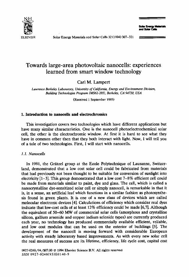
Towards large-area photovoltaic nanocells: experiences ... · Towards large-area photovoltaic...
15
ELSEVIER Solar Energy Materials and Solar Cells 32 (1994) 307-321 ~ r ~ w k ma ~¢,olk Towards large-area photovoltaic nanocells: experiences learned from smart window technology Carl M. Lampert Lawrence Berkeley Laboratory, Universityof California, Energy and Environment Division, Building TechnologiesProgram (MS62-203), Berkeley, CA 94720, USA (Received 1 September 1993) 1. Introduction to nanocells and electrochromics This investigation covers two technologies which have different applications but have many similar characteristics. One is the nanocell photoelectrochemical solar cell, the other is the electrochromic window. At first it is hard to see what they have in common other then that they both interact with light. Now, I will tell you of a tale of two technologies. First, I will start with nanocells. 1.1. Nanocells In 1991, the Gr~itzel group at the Ecole Polytechnique of Lausanne, Switzer- land, demonstrated that a low cost solar cell could be fabricated from materials that had previously not been thought to be suitable for conversion of sunlight into electricity [1-3]. This group demonstrated that a low cost 7-8% efficient cell could be made from materials similar to paint, dye and glass. The cell, which is called a nanocrystalline dye-sensitized solar cell or simply nanocell, is remarkable in that it is, in a sense, an artificial leaf which functions in a similar fashion as photosynthe- sis found in green plants. It is one of a new class of devices which are called molecular electronic devices [4]. Calculations of efficiency which consider real dyes indicate that low-cost cells of at least 12% efficiency could be made [6,7]. Although the equivalent of 50-60 MW of commercial solar ceils (amorphous and crystalline silicon, gallium arsenide and copper indium selenide types) are currently produced each year, no technology has produced commercially available efficient, reliable, and low cost modules that can be used on the exterior of buildings [5]. The development of the nanocell is moving forward with considerable European activity with steady laboratory based improvements. As with every new solar cell the real measures of success are its lifetime, efficiency, life cycle cost, capital cost 0927-0248/94/$07.00 © 1994 Elsevier Science B.V. All rights reserved SSDI 0927-0248(93)E0140-9
Transcript of Towards large-area photovoltaic nanocells: experiences ... · Towards large-area photovoltaic...
ELSEVIER Solar Energy Materials and Solar Cells 32 (1994) 307-321
~ r ~ w k ma ~ ¢ , o l k
Towards large-area photovoltaic nanocells: experiences learned from smart window technology
Carl M. Lamper t
Lawrence Berkeley Laboratory, University of California, Energy and Environment Division, Building Technologies Program (MS62-203), Berkeley, CA 94720, USA
(Received 1 September 1993)
1. Introduction to nanocells and electrochromics
This investigation covers two technologies which have different applications but have many similar characteristics. One is the nanocell photoelectrochemical solar cell, the other is the electrochromic window. At first it is hard to see what they have in common other then that they both interact with light. Now, I will tell you of a tale of two technologies. First, I will start with nanocells.
1.1. Nanocells
In 1991, the Gr~itzel group at the Ecole Polytechnique of Lausanne, Switzer- land, demonstrated that a low cost solar cell could be fabricated from materials that had previously not been thought to be suitable for conversion of sunlight into electricity [1-3]. This group demonstrated that a low cost 7-8% efficient cell could be made from materials similar to paint, dye and glass. The cell, which is called a nanocrystalline dye-sensitized solar cell or simply nanocell, is remarkable in that it is, in a sense, an artificial leaf which functions in a similar fashion as photosynthe- sis found in green plants. It is one of a new class of devices which are called molecular electronic devices [4]. Calculations of efficiency which consider real dyes indicate that low-cost cells of at least 12% efficiency could be made [6,7]. Although the equivalent of 50-60 MW of commercial solar ceils (amorphous and crystalline silicon, gallium arsenide and copper indium selenide types) are currently produced each year, no technology has produced commercially available efficient, reliable, and low cost modules that can be used on the exterior of buildings [5]. The development of the nanocell is moving forward with considerable European activity with steady laboratory based improvements. As with every new solar cell the real measures of success are its lifetime, efficiency, life cycle cost, capital cost
0927-0248/94/$07.00 © 1994 Elsevier Science B.V. All rights reserved SSDI 0 9 2 7 - 0 2 4 8 ( 9 3 ) E 0 1 4 0 - 9
308 C.M. Lampert / Solar Energy Materials and Solar Cells 32 (1994) 307-321
to build a production plant, and its actual cost to manufacture. The estimated cost of the nanocell is $100-150/m 2 or lower. Currently, the lifetime of nanocell is not known, but they have performed well under laboratory testing.
1.2. Electrochromics
Now, in a parallel field of development electrochromics are being developed for both small and large are applications [8]. Many small size (under 0.25 m 2) products are being introduced in the marketplace. Electrochromics are an important part of a larger category of switchable materials known as chromogenics [9]. The funda- mental property of an electrochromic material is that it exhibits a large change in optical properties upon a change in either electric field. This optical change results in a transformation from a highly transmitting state to a partly reflecting or absorbing state, either totally or partly over the visible and solar spectrum.
The practical use of electrochromics has been known since about 1970. During the middle of the 1970's, many small digital information displays were developed, but the technology could not compete with the advance of liquid crystals for displays. Renewed interest in the area of electrochromics started again in the mid-1980's for large area applications such as for automotive nurrors and windows for cars and buildings. This area of development has been growing ever since that time. Electrochromic optical switching devices known as "smart windows" can be used for a variety of applications. One of the most promising applications is for the regulation of incident solar energy and glare in buildings, vehicles, aircraft, spacecraft and ships. The world-wide production of flat glass is about 1 billion m 2 per year. In the US alone, glass production is about 470 million m 2 per year (1988), with about 25% for buildings and 11% for automobiles, so the potential for glass based glazings technology is very large. An example in how quickly new glazing products can penetrate the market, in just a few years, low emissivity or low coatings (some of these are transparent conductors) for windows have gained about 25% of the US residential glazing market. Low-e coatings are used to reduce the radiative portion of heat transfer from glass surfaces. Electrochromic products already in the marketplace are automobile mirrors which can automatically regu- late glare according to light levels. Prototypes are being tested for automobile sun-roofs and visors. Future applications include automobile side and rear win- dows, architectural glazing and aircraft windows. Chromogenic devices can also be used for large-area information displays in applications where high switching speed is not required, such as for airport display boards. Also electrochromic eyeglasses are being introduced as products by Nikon (Tokyo, Japan) in Japan and being developed by Eyeonics (Portland, OR) and PPG (Pittsburg, PA) Companies.
The function of an electrochromic device, used in a glazing, is to control the flow of light or solar energy, according to an energy management scheme or the desire of the user. This technology can regulate lighting and heating levels for energy load reduction [10-11]. Substantial savings in lighting and cooling energy consumption and installed equipment costs can be realized. From a privacy viewpoint, this technology may have a significant advantage over existing blinds
C.M. Lampert / Solar Energy Materials and Solar Cells 32 (1994) 307-321 309
and drapes. In the last few years there has been significant growing interest in this technology and it is expected to be used in products into the next century.
One of the most significant issues is the cost of these devices and the trade-offs between cost and benefit, and cost and lifetime. The electrochromic window cost has been estimated to range from 100-1000 US$/m 2. Some companies have set cost goals of 100-250 US$/m 2. These cost goals are about the same as for nanocells.
2. Device construction
Now we will discuss the construction of both nanocell and electrochromic devices and begin to show their similarities.
2.1. Nanocells
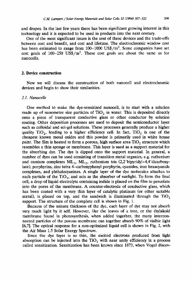
One method t0 make the dye-sensitized nanocell, is to start with a solution made up of nanometre size particles of TiO 2 in water. This is deposited directly onto a piece of transparent conductive glass or other conductor by solution coating. Other deposition processes are used to deposit the semiconductor layer such as colloidal and sol-gel solutions. These processes generally produce a higher quality TiO2, leading to a higher efficiency cell. In fact, TiO 2 is one of the cheapest known metal oxides and this powder is primarily used in white house paint. The film is heated to form a porous, high surface area TiO2 structure which resembles a thin sponge or membrane. This layer is used as a support material for the absorbing dye. The dye is dipped onto the support material. In general, a number of dyes can be used consisting of transition metal organics, e.g. ruthenium and osmium complexes ML3, ML2, ruthenium tris (2,2'bipyridyl-4,4'dicarboxy- late), porphyrins, zinc tetra 4-carboxyphenyl porphyrin, cyanides, iron hexacyanide complexes, and phthalocyanines. A single layer of the dye molecules attaches to each particle of the TiO2, and acts as the absorber of sunlight. To form the final cell, a drop of liquid electrolyte containing iodide is placed on the film to percolate into the pores of the membrane. A counter-electrode of conductive glass, which has been coated with a very thin layer of catalytic platinum (or other suitable metal), is placed on top, and the sandwich is illuminated through the TiO 2 support. The structure of the complete cell is shown in Fig. 1.
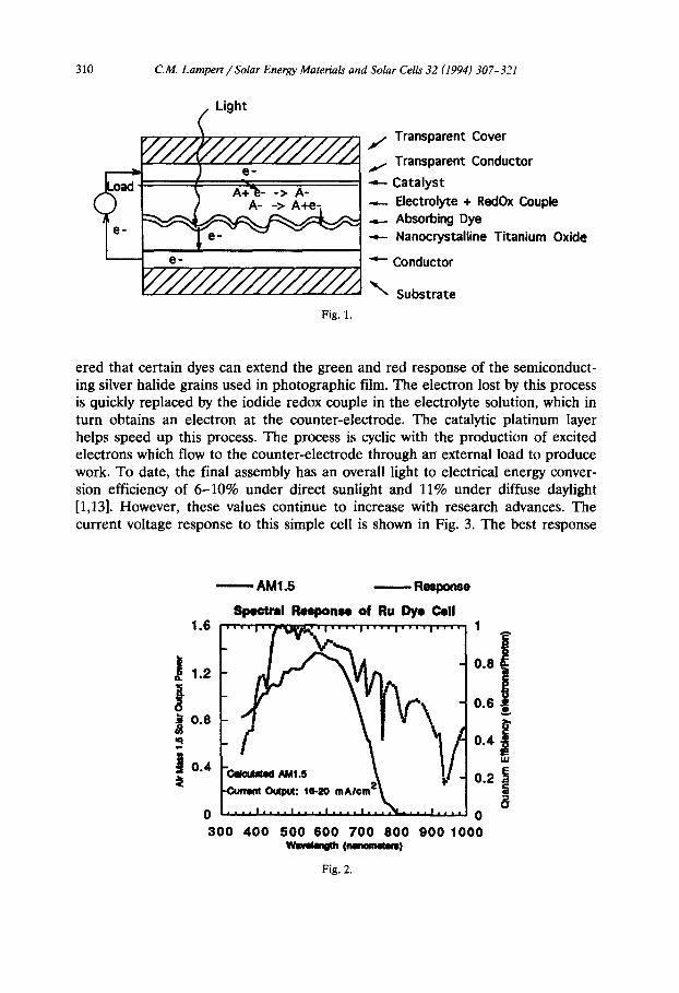
Because of the minute thickness of the dye, each layer of dye may not absorb very much light by it self. However, like the leaves of a tree, or the thylakoid membrane found in photosynthesis, when added together, the many intercon- nected particles of the porous membrane can together absorb 90% of visible light [6,7]. The optical response for a non-optimized liquid cell is shown in Fig. 2, with the Air Mass 1.5 Solar Energy Spectrum.
Since the dye layer is so thin, the excited electrons produced from light absorption can be injected into the TiO 2 with near unity efficiency in a process called sensitization. Sensitization has been known since 1873, when Vogel discov-
310 C.M. Lampert / Solar Energy Materials and Solar Cells 32 (1994) 307-321
Light
e-
~f. Transparent Cover
~ . Transparent Conductor
4 - Catalyst Electrolyte + RedOx Couple Absorbing Dye
~-- Nanocrystalline Titanium Oxide
~-- Conductor
~ - Substrate
Fig. 1.
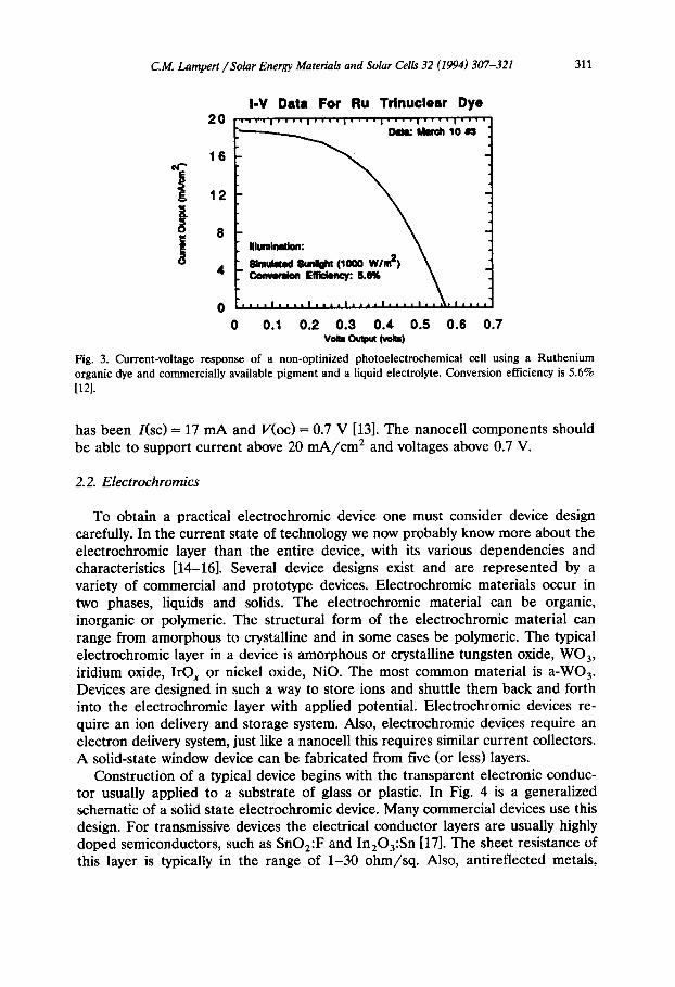
ered that certain dyes can extend the green and red response of the semiconduct- ing silver halide grains used in photographic film. The electron lost by this process is quickly replaced by the iodide redox couple in the electrolyte solution, which in turn obtains an electron at the counter-electrode. The catalytic platinum layer helps speed up this process. The process is cyclic with the production of excited electrons which flow to the counter-electrode through an external load to produce work. To date, the final assembly has an overall light to electrical energy conver- sion efficiency of 6-10% under direct sunlight and 11% under diffuse daylight [1,13]. However, these values continue to increase with research advances. The current voltage response to this simple cell is shown in Fig. 3. The best response
AM1.5 Response
Spectral Response of Ru Dye Cell 1.6 1
i i'i i.. i a
a 0 0 300 400 500 600 700 800 900 1000
Wwek.~h (Mnmcws)
Fig. 2.
C.M. Lampert / Solar Energy Materials and Solar Cells 32 (1994) 307-321 311
I - V D a t a F o r R u T r l n u c i e a r D y e
2 0 . . . . , . . . . , . . . . , . . . . i . . . . , . . . . , . . . .
16
8
L \
0 I I I I ' I ' ' ' ' I ~ ~ 1 ~ ' 1 ~ ' I ' ' ~ I ' ~ a J
0 0 . 1 0 . 2 0 . 3 0 . 4 0 . 5 0 . 6 0 . 7 v ~ Outpm (voh)
Fig. 3. Current-voltage response of a non-optinized photoelectrochemical cell using a Ruthenium organic dye and commercially available pigment and a liquid electrolyte. Conversion efficiency is 5.6% [12].
has been /(sc) = 17 mA and V(oc) = 0.7 V [13]. The nanoceU components should be able to support current above 20 m A / c m 2 and voltages above 0.7 V.
2.2. Electrochromics
To obtain a practical electrochromic device one must consider device design carefully. In the current state of technology we now probably know more about the electrochromic layer than the entire device, with its various dependencies and characteristics [14-16]. Several device designs exist and are represented by a variety of commercial and prototype devices. Electrochromic materials occur in two phases, liquids and solids. The electrochromic material can be organic, inorganic or polymeric. The structural form of the electrochromic material can range from amorphous to crystalline and in some cases be polymeric. The typical electrochromic layer in a device is amorphous or crystalline tungsten oxide, WO 3, iridium oxide, IrO x or nickel oxide, NiO. The most common material is a-WO 3. Devices are designed in such a way to store ions and shuttle them back and forth into the electrochromic layer with applied potential. Electrochromic devices re- quire an ion delivery and storage system. Also, electrochromic devices require an electron delivery system, just like a nanocell this requires similar current collectors. A solid-state window device can be fabricated from five (or less) layers.
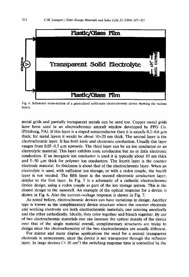
Construction of a typical device begins with the transparent electronic conduc- tor usually applied to a substrate of glass or plastic. In Fig. 4 is a generalized schematic of a solid state electrochromic device. Many commercial devices use this design. For transmissive devices the electrical conductor layers are usually highly doped semiconductors, such as SnO2:F and InEOa:Sn [17]. The sheet resistance of this layer is typically in the range of 1-30 ohm/sq . Also, antireflected metals,
312 C.M. Lampert // Solar Energy Materials and Solar Cells 32 (1994) 307-321
Fig. 4. Schematic cross-section of a generalized solid-state electrochromic device showing the various layers.
metal grids and partially transparent metals can be used too. Copper metal grids have been used in an electrochromic aircraft window developed by PPG Co. (Pittsburg, PA). If this layer is a doped semiconductor then it is usually 0.2-0.6 Ixm thick; for metal layers it would be about 10-20 nm thick. The second layer is the electrochromic layer. It has both ionic and electronic conduction. Usually this layer ranges from 0.05-0.3 ~m upwards. The third layer can be an ion conductor or an electrolytic material. This layer exhibits ionic conduction but no or little electronic conduction. If an inorganic ion conductor is used it is typically about 10 nm thick and 5-50 ~zm thick for polymer ion conductors. The fourth layer is the counter electrode material. Its thickness is about that of the electrochromic layer. When an electrolyte is used, with sufficient ion storage, or with a redox couple, the fourth layer is not needed. The fifth layer is the second electronic conduction layer, similar to the first layer. In Fig. 5 is a schematic of a cathodic electrochromic device design, using a redox couple as part of the ion storage system. This is the closest design to the nanocell. An example of the optical response for a device is shown in Fig. 6. Also the current-voltage response is shown in Fig. 7.
As noted before, electrochromic devices can have variations in design. Another type is known as the complimentary device structure where the counter electrode and working electrode are both electrochromic materials, one coloring anodically and the other cathodically. Ideally, they color together and bleach together. By use of two electrochromic materials one can increase the optical density of the device over that of the single material overall, complimentary structures are tricky to design since the electrochemistry of the two electrochromics are usually different.
For mirror and many display applications the need for a second transparent electrode is unnecessary, since the device is not transparent through the reflector layer. In large devices (> 30 cm 2) the switching response time is controlled by the

C.M. Lampert / Solar Energy Materials and Solar Cells 32 (1994) 307-321 313
v oc V / / / / / / / / / / / / / / / , ' A
A- -> A+e- A+ e- -> A-
i Colors A+ 1 Bleach L ~ c e l 4 e
- '+
; Fig. 5.
~,/ Transparent Cover
~ . Transparent Conductor
-4- Electrolyte + RedOx Couple
-~- Cathodic Electrochromic
"'-'Transparent Conductor
~ " Transparent Substrate
conductivity of the transparent conductors. In large devices it is critical that the voltage drop across the conductors is not too great or only part of the device will switch.
Example electrochromic device structures are given in Table 1. In this list of examples, several complimentary devices are noted. In the Nissan window, ca- thodic a-WO 3 and anodic Prussian Blue (Fe4(Fe(CN))6) 3 are coupled together
100
Q ¢J i,- M
t -
l - -
E 0 z
8 0 -
6 0 -
4 0
20
0 2 0 0
Tungsten Oxide/a-PEOILKX1)SRPE
S~Jched, 1 .0V
- - - C o l o r e d . - 1 . z V
I I I " - 1 - - - - ' - t - - - - - ~ I 4 0 0 6 0 0 8 0 0 1 0 0 0
w~eten~ (m)
Fig. 6.
314 C.M. Lampert / Solar Energy Materials and Solar Cells 32 (1994) 307-321
0.1
EO.O5
0 _
~ . 0 5 --
J/ I I
- I .0 0
Potential (V)
-0.1 I -Z.O 1.0 2.0
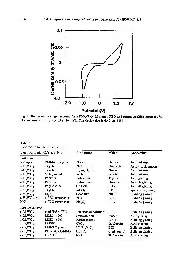
Fig. 7. The current-voltage response for a I T O / W O 'Lithium a-PEO and organodisulfide complex/flu electrochromic device, cycled at 20 mVis. The device size is 4×3 cm. [18].
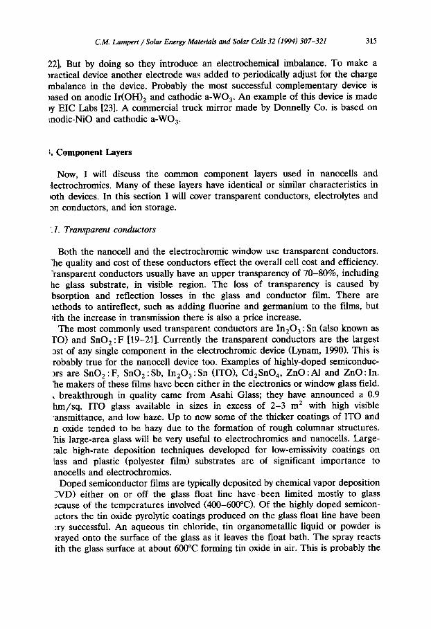
Table 1 Electrochromic device structures
Electrochromic IC/electrolyte Ion storage Maker Application
Proton Systems Viologen PMMA + organic None Gentex Auto mirrors a-HxWO 3 Ta205 NiO Donnelly Auto/ t ruck mirrors a-HxWO 3 TazO 5 IrxSnrO z : F Nikon Auto mirrors a-HxWO 3 SiO z /meta l WO 3 Schott Auto mirrors a-HxWO 3 Polymer Polyaniline Toyota Auto glazing a-HxWO 3 Polymer Polyaniline Dornier Aircraft glazing a-HxWO 3 Poly-AMPS Cu Grid PPG Aircraft glazing a-H~WO 3 Ta205 a-IrO 2 EIC Spacecraft glazing a-HxWO 3 MgF 2 Gold film NREL Building glazing a-H xWO3 : Mo a-PEO copolymer NiO LBL Building glazing NiO a-PEO copolymer Nb205 LBL Building glazing
Lithium systems a-LixWO 3 modified a-PEO Ion storage polymer LBL Building glazing a-Li,,WO 3 LiCIO4 + PC Prussian blue Nissan Auto glazing a-LixWO 3 LiClO 4 + PC Redox couple Asahi Building glazing a-LixWO 3 Li-PEO CeO x St. Gobain Auto glazing a-LixWO 3 Li-B-SiO glass IC/LixV205 EIC Building glazing a-LixWO3 PPG-LiC1Oa-MMA LiyV205 Chalmers U. Building glazing a-LixWO 3 Li-PEO NiO St. Gobain Auto glazing
C.M. Lampert / Solar Energy Materials and Solar Cells 32 (1994) 307-321 315
22]. But by doing so they introduce an electrochemical imbalance. To make a ~ractical device another electrode was added to periodically adjust for the charge mbalance in the device. Probably the most successful complementary device is ,ased on anodic Ir(OH) 2 and cathodic a-WO3. An example of this device is made ~y EIC Labs [23]. A commercial truck mirror made by Donnelly Co. is based on modic-NiO and cathodic a-WO 3.
;. Component Layers
Now, I will discuss the common component layers used in nanocells and :lectrochromics. Many of these layers have identical or similar characteristics in ,oth devices. In this section I will cover transparent conductors, electrolytes and an conductors, and ion storage.
'.1. Transparent conductors
Both the nanocell and the electrochromic window use transparent conductors. "he quality and cost of these conductors effect the overall cell cost and efficiency. "ransparent conductors usually have an upper transparency of 70-80%, including he glass substrate, in visible region. The loss of transparency is caused by bsorption and reflection losses in the glass and conductor film. There are aethods to antireflect, such as adding fluorine and germanium to the films, but 6th the increase in transmission there is also a price increase.
The most commonly used transparent conductors are In20 3 : Sn (also known as I'O) and SnO2:F [19-21]. Currently the transparent conductors are the largest ost of any single component in the electrochromic device (Lynam, 1990). This is robably true for the nanocell device too. Examples of highly-doped semiconduc- )rs are SnO 2 : F, SnO2 : Sb, In20 3 : Sn (ITO), Cd2SnO4, ZnO : ml and ZnO : In. 'he makers of these films have been either in the electronics or window glass field. • breakthrough in quality came from Asahi Glass; they have announced a 0.9 hm/sq. ITO glass available in sizes in excess of 2-3 m z with high visible • ansmittance, and low haze. Up to now some of the thicker coatings of ITO and n oxide tended to be hazy due to the formation of rough columnar structures. 'his large-area glass will be very useful to electrochromics and nanocells. Large- :ale high-rate deposition techniques developed for low-emissivity coatings on lass and plastic (polyester film) substrates are of significant importance to anocells and electrochromics.
Doped semiconductor films are typically deposited by chemical vapor deposition 2VD) either on or off the glass float line have been limited mostly to glass ~cause of the temperatures involved (400-600°C). Of the highly doped semicon- actors the tin oxide pyrolytic coatings produced on the glass float line have been • .ry successful. An aqueous tin chloride, tin organometallic liquid or powder is ~rayed onto the surface of the glass as it leaves the float bath. The spray reacts ith the glass surface at about 600°C forming tin oxide in air. This is probably the

316 C.M. Lampert / Solar Energy Materials and Solar Cells 32 (1994) 307-321
most efficient coating process for glass coating. Problems of iridescence have hampered the use of this glass compared to the multilayer coated glass with much more controllable optical and lower emissivity. Recently, these coatings have been improved by Pilkington (K-Glass) and LOF glass by the use of a two layer coating to reduce iridescence of thicker tin oxide coatings. This allows coated glass with even lower sheet resistance (8-10 ohms/sq.) then before to be produced with excellent optical properties. CVD conveyor furnaces have been used for electronic film production for many years. The thermal, mechanical and chemical stability of the substrate are significant in determination of the proper deposition technique and conditions. With CVD, secondary and competing reactions must be sup- pressed by control of reaction kinetics and knowledge of the system thermodynam- ics. Also, thermal durability and property stability of substrate and film is signifi- cant for long-life designs. There is considerable commercialization in both multi- layer and semiconductor low emissivity coatings in Europe, North America, Japan and Russia.
Also, doped semiconductors can be deposited by PVD, but at lower deposition rates. A new conductive coating of ZnOxFy has been produced for a CVD float line process [24]. Furthermore, gradient index transparent conductors are yet to be developed. It is possible that some of the surface texturing studies performed on transparent semiconductors for photovoltaics may be useful for low-e applications coatings. Obtaining a reproducible high-quality commercial coating on plastic is considerably more difficult than making research grade films. Commercially ITO coated polyester is available at 20-30 ohms/sq. Example manufactures are South- wall (Palo Alto, CA) and Courtaulds (UK). Present techniques need to be improved to deposit coatings at low temperatures to get very low sheet resistances (10 ohm/sq.), high mobility and high transmission on polymeric substrates.
Mesh low-emissivity coatings are made from metals or highly doped transparent semiconductors, metals. The mesh pattern allows higher transmission than contin- uous coatings. The mesh pattern is etched in the surface using photolithography. The theory of mesh low-e films has been developed. Also, several fabrications of experimental films have been made [25-28]. One design involves chemical etching of the surface of a ITO film to form a regular grid pattern [29]. The etched grid consists of square openings of d = 2.5 I~m. For this grid, T s increased from 0.8 to 0.9 while reflectance decreased from 0.91 to 0.83. Metal grids can be used to make transparent low-e coatings too. The best modeled results for metallic grids were obtained for aluminum and magnesium where the line width would have to he about 0.1 ~m to give T s = 0.90 and R = 0.90 [27].
Other materials of interest are doped ZnO and polymer conductors, this cost will decrease. Zinc oxide is interesting as a transparent conductor used in a polymer containing system, since it absorbs much of the UV from the sun.
3. 2. Ion conductors and electrolytes
In different configurations of electrochromic devices, a solid ion conductor or a solid electrolytes are used. In the nanocells only liquid electrolytes have been used
C.M. Lampert / Solar Energy Materials and Solar Cells 32 (1994) 307-321
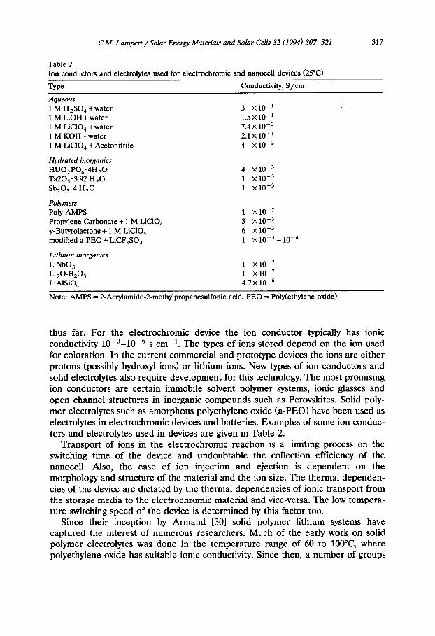
Table 2 Ion conductors and electrolytes used for electrochromic and nanocell devices (25°C)
317
Type Conductivity, S / c m
Aqueous 1 M H 2 S O 4 + w a t e r 3 ×10 -1 1 M LiOH + water 1.5 x 10- t 1 M LiCIO 4 +water 7.4x 10 -2 1 M KOH +water 2.1 × 10 -1 1 M LiCIO 4 +Acetonitrile 4 x 10 -2
Hydrated inorganics HUO2PO4.4H20 4 × i 0 -3 Ta205-3.92 H 2 0 1 x l 0 -3 Sb205.4 H 2 0 1 ×10 -3
Polymers Poly-AMPS 1 x 10 -2 Propylene Carbonate + 1 M LiC104 3 x 10 -3 y-Butyrolactone+ 1 M LiC104 6 × 10 -3 modified a-PEO+LiCF3SO 3 1 x 10 -3 - 10 -4
Lithium inorganics LiNbO 3 1 x 10 -7 Li20-B20 3 1 x 10 -7 LiAISiO 4 4.7 x 10⁻⁶
Note: AMPS = 2-Acrylamido-2-methylpropanesulfonic acid, PEO = Poly(ethylene oxide).
thus far. For the electrochromic device the ion conductor typically has ionic conductivity 10-3-10 -6 s cm -1. The types of ions stored depend on the ion used for coloration. In the current commercial and prototype devices the ions are either protons (possibly hydroxyl ions) or lithium ions. New types of ion conductors and solid electrolytes also require development for this technology. The most promising ion conductors are certain immobile solvent polymer systems, ionic glasses and open channel structures in inorganic compounds such as Perovskites. Solid poly- mer electrolytes such as amorphous polyethylene oxide (a-PEO) have been used as electrolytes in electrochromic devices and batteries. Examples of some ion conduc- tors and electrolytes used in devices are given in Table 2.
Transport of ions in the electrochromic reaction is a limiting process on the switching time of the device and undoubtable the collection efficiency of the nanocell. Also, the ease of ion injection and ejection is dependent on the morphology and structure of the material and the ion size. The thermal dependen- cies of the device are dictated by the thermal dependencies of ionic transport from the storage media to the electrochromic material and vice-versa. The low tempera- ture switching speed of the device is determined by this factor too.
Since their inception by Armand [30] solid polymer lithium systems have captured the interest of numerous researchers. Much of the early work on solid polymer electrolytes was done in the temperature range of 60 to 100°C, where polyethylene oxide has suitable ionic conductivity. Since then, a number of groups
318 C.M. Lampert / Solar Energy Materials and Solar Cells 32 (1994) 307-321
have reported solid polymer electrolytes with acceptable conductivity and ambient temperature [31], significantly broadening the scope of applications for solid polymer electrolytes.
3.3. Ion storage components and redox couples
Ion storage are one of the hardest areas of development for electrochromics. Ion storage media for electrochromics may be non-electrochromic materials or may also have electrochromic characteristics. As long as they are complimentary to the active electrochromic materials. It is important that the ion storage material has ion storage characteristics (charge capacity) that active electrochromic material matches. Finding well balanced and low potential redox system is very difficult. Iodides have been used in some polymer prototype devices. Polyaniline as a complimentary ion storage layer has been used by Dornier (Germany), Toyota, Nissan and General Glass in Japan have used Prussian Blue for the same purpose. In nanocells the majority of the cells have been made with iodine/ iodide and bromide redox couples. Unfortunately, both of these ions migrate throughout the device.
The approach in our laboratory for electrochromic devices has included the use of solid polymer electrolytes in combination with polyorganodisulfides or polythiols [18,32,33]. These materials are termed solid redox polymer electrodes (SRPE's) to reflect the dynamic process of polymerization depolymerization that occurs as these electrodes are oxidized and reduced. Considerable success has come from the use of SRPE's in lithium polymer batteries.
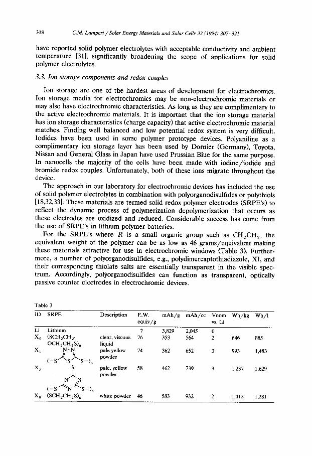
For the SRPE's where R is a small organic group such as CH2CH2, the equivalent weight of the polymer can be as low as 46 grams/equivalent making these materials attractive for use in electrochromic windows (Table 3). Further- more, a number of polyorganodisulfides, e.g., polydimercaptothiadiazole, XI, and their corresponding thiolate salts are essentially transparent in the visible spec- trum. Accordingly, polyorganodisulfides can function as transparent, optically passive counter electrodes in electrochromic devices.
Table 3
ID SRPE Description E . W . mAh/g mAh/cc Vnom Wh/kg Wh/l equiv/g vs. Li
Li Lithium 7 3,829 2,045 0 X 0 (SCH2CH 2- clear, viscous 76 353 564 2 646 885
OCH 2CH z S)n liquid X I N-N pale yellow 74 362 652 3 993 1,483
(_ S...~S.~..S_) n powder
X 5 S pale, yellow 58 462 739 3 1,237 1,629
( -S / '~N@~S- )n powder
X 8 ( S C H 2 C H 2 S ) n white powder 46 583 932 2 1,012 1,281
C.M. Lampert / Solar Energy Materials and Solar Cells 32 (1994) 307-321 319
In a typical device, metal oxide insertion (or intercalation) electrodes are chosen such that coloration of the electrochromic electrode occurs upon application of a sufficient voltage bias across the cell. An example is, one of the electrodes colors upon oxidation while the other electrode is usually passive upon reduction; similarly upon application of a sufficient reverse bias, complementary bleaching of the two electrodes occurs. However, upon prolonged cycling, parasitic reactions may reduce the capacity of one electrode, even if the electrodes were matched initially. The device then become unbalanced and is unable to bleach fully. One way to avoid this problem is to use an optically passive ion storage electrode that undergoes redox without an associated color change. Since the majority of the known electrochromic electrodes reversibly insert (or intercalate) cations, a suit- able redox electrode would possess electroactive anions such as the organothio- lates. The pertinent half-reaction for coloring and bleaching WO 3 can be repre- sented as,
WO3(bleached ) + n e - + n L i + ~ LinWO3(colored ) ,
and for the SRPE,
nLi2(SRS ) ~, (SRS)n + 2nLi++ 2ne-(passive),
giving a cell reaction for the electrochromic device as
WO3(bleached ) + nLi2(SRS ) ,a, (SRS)~ + Li2~WO3(colored).
In the case of an optically passive SRPE, the capacity need not be matched to the electrochromic electrode, but rather would be formulated with excess capacity. The role of polymer redox materials for nanocells is not certain but it m a y b e worth experimentation.
4. Conclusions
The Electrochromic and the Nanocell have a lot in common. They both have an electrolyte system which for the electrochromic can contain a variety of redox or ion storage layers. Generally, the nanocell uses a I or Br redox couple. They are both dependent on transparent conductors on glass or plastic. They require the lowest possible conductivity 1-10 ohm/sq, and require 1-2 layers for each device. The current and voltage requirement are different for the two devices. T h e voltage, current 0.6 V, 15-20 mA/sq.cm is the peak output for the nanocell and 1-3 V, 0.1-0.2 mA/sq.cm is the maximum input for an electrochromic window. The current requirement on the electrolyte for the nano cell are 100 times that of the electrochromic. This may present a problem in the replacement of liquid electrolytes with lower conducting solid state ones. The transparent conductors are a significant cost in both devices. They require efficient, low potential redox systems. Their performance depends on the microstructure of the active material. It appears that the nanocell is more dependent on microstructure, although both devices require an open microstructure for fast transport of ions or electrons. They

320 C.M. Lampert / Solar Energy Materials and Solar Cells 32 (1994) 307-321
share similar durability and cost goals. They both have cost goals of about $USlO0-150/sq m or less in pence. Both cells need to have 10-30 year lifetime. Development of industrial scale production techniques to fabricate entire cells is key to cost.
5. Acknowledgements
The author wishes to thank Prof. M. Gr[itzel (EPFL, Lausanne, Switzerland) and A. Zichichi, The World Lab. and the Goverment of Italy for the opportunity to give this lecture at the Ettore Majorana Centre for Scientific Culture. The author also wishes to thank G. Smestad (PSI, Switzerland) for supplying data on nanocells.
This work was performed at the Lawrence Berkeley Laboratory, under the Energy and Environment Division. The work was funded in part by the Assistant Secretary for Conservation and Renewable Energy, Office of Building Technolo- gies, Building Systems and Materials Division of the U.S. Department of Energy under contract No. DE-AC03-76SF00098.
6. References
[1] B. O'Regan, M. Gr~itzei, Nature 353 (1991) 737-739. [2] T. Beardsley, Scientific American, Jan. (1992) 138. [3] M. Gr~itzel, The World and I, The Washington Times Corp., Washington, Feb. (1993) 228-235. [4] D. Bradley, Science 259 (1993) 890-892. [5] K. Zweibel, Harnessing Solar Power: The Photovoltaics Challenge (Plenum Press, NY, 1990). [6] G. Smestad and H. Ries, Sol. Energy Mater. Sol. Cells 25 (1992) 51-71. [7] A. De Vos, Endoreversible Thermodynamics of Solar Energy Conversion (Oxford University Press,
Oxford, 1992). [8] C.M. Lampert and C.G. Granqvist (Eds.), Large-area Chromogenics: Materials and devices for
transmittance control (Optical Engineering Press-SPIE, Bellingham, WA, 1990). [9] C.M. Lampert, Electrochromic materials and devices for energy efficient windows, Sol. Energy
Mater. 11 (1984) 1. [10] S. Selkowitz and C.M. Lampert, in: C.M. Lampert and C.G. Granqvist (Eds.), Large-area
Chromogenics: Materials and Devices for Transmittance Control (Optical Engineering Press SPIE, Bellingham, WA, 1990) p. 504.
[11] S. Reilly, D. Arasteh and S. Seikowitz, Thermal and optical analysis of switchable window glazings, Sol. Energy Mater. 22 (1991) 1.
[12] G. Smestad, PSI Switzerland, private communication. [13] M.K. Nazeeruddin, A. Kay, I. Rodicio, R. Humphry-Baker, E. Miller, P. Liska, N Vlachopouios
and M. Gr~itzel, J. Am. Chem. Soc. 115 (1993) 6382-6390. [14] W.C. Dautremont-Smith, Transition metal oxide electrochromic materials and displays: A review,
Displays 4-3 (1982) 67. [15] A. Donnadieu, Electrochromic materials, Mat. Sci. Eng. B3 (1989) 185-195. [16] C.M. Lampert , Electrochromic materials and devices for energy efficient windows, Sol. Energy
Mater. 11 (1984) 1. [17] J.L. Vossen, Transparent conducting films, in: G. Hass, M. Francombe and R. Hoffman (Eds.),
Physics of Thin Films (Academic Press, NY, 1977).

C.M. Lampert / Solar Energy Materials and Solar Cells 32 (1994) 307-321 321
[18] C.M. Lampert, S.J. Visco, M.M. Doeff, Y. Ma, Y. He and J.C., Giron characteristics of laminated electrochromic devices using polyorganodisulfide electrodes, Proc. SPIE 2017 (1993) in press.
[19] G. Haacke, Transparent conducting oxides, Ann. Rev. Mat. Sci. 7 (1977) 73. [20] C.M. Lampert, Heat-mirror coatings for energy conserving windows, Sol. Energy Mater. 6 (1981) 1. [21] C.M. Lampert, Materials chemistry and optical properties of transparent conductive thin films for
solar energy utilization, Ind. Eng. Chem. Prod. R and D 21 (1982) 61. [22] T. Kase et al., Performance of tungsten oxide/Prussian blue device. [23] S.F. Cogan and R.D. Rauh, The a-WO 3/a-IrO 2 Electrochromic System, in: C.M. Lampert and
C.G. Granqvist (Eds.), Large-Area Chromogenics: Materials and Devices for Transmittance Control (Optical Engineering Press, SPIE, Bellingham, WA, 1990).
[24] R. Gordon, Zinc oxyfluoride transparent conductor, US Patent 4, 990, 286, Feb. 5 (1991). [25] R.C. McPhedron and D. Maystre, On the theory and solar application of inductive grids, Appl.
Phys. 14 (1977) 1. [26] D. Maystre and M.J. Nevieve, Opt. 9 (1979) 301. [27] D. Pramanik, A.J. Sievers and R.H. Silsbee, Sol. Energy Mater. 2 (1979) 81. [28] A.J. Sievers, in: L.E. Murr (Ed.), Solar Materials Science (Academic Press, NY, 1980) p. 255. [29] J.C.C. Fan, F.J. Bachner and G.H. Foley, Appl. Phys. Lett. 31 (1977) 773. [30] M.B. Armand, J.M. Chabagno and M.J. Duclot, Fast ion transport, in: P. Vashista, J.N. Mundy
and G.K. Shenoy (Ed.), Solids (Elsevier, Amsterdam, 1979) p. 131. [31] C. Booth, C.V. Nicholas and D.J. Wilson, in: J.R. MacCallun and C.A. Vincent (Eds.), Polymer
Electrolyte Reviews (Elsevier, Amsterdam, 1989) p. 229. [32] C.M. Lampert and S.J. Visco, Electrochromic optical switching device, US 5, 142, 406, 1992. [33] C.M. Lampert, M.C. Doeff, S.J. Visco and Y.P. Ma, Patent Pending, 1993.