Towards an Inductively Coupled Power/Data Link …Towards an Inductively Coupled Power/Data Link for...
4
Towards an Inductively Coupled Power/Data Link for Bondpad-less Silicon Chips Song Luan * , Amir Eftekhar *† , Olive H. Murphy *† and Timothy G. Constandinou *† * Department of Electrical and Electronic Engineering, Imperial College London, SW7 2BT, UK † Centre for Bio-Inspired Technology, Institute of Biomedical Engineering, Imperial College London, SW7 2AZ, UK Email: {song.luan09, a.eftekhar, o.murphy, t.constandinou}@imperial.ac.uk Abstract— This paper explores the concept of developing a bondpad-less fully-integrated inductive link for power/data trans- fer between a CMOS Integrated Circuit (IC) and a PCB. A key feature of the implemented system is that it requires no off- chip components. The proposed chip uses a standard 0.35 μm process and occupies an area of 2.5 mm×2.5 mm and an on-chip inductor occupies an area of 1.5 mm×1.5 mm. At 900 MHz, 9 mW was designed to be provided to the chip (up to 22.5 mW with a total efficiency of 5 %). Binary Phase Shift Keying (BPSK) and Load shift keying (LSK) are used for the the PCB-to-chip and chip-to-PCB link respectively for half-duplex communication. An Injection-Locked-Oscillator-based BPSK demodulator is imple- mented on-chip to save power. The maximum data rate for the PCB-to-chip link is 10 Mb/s. The estimated area of the circuitry is only 2 mm 2 which is 32 % of the total chip area. I. I NTRODUCTION Commercially-available ICs, such as the Central Processing Units (CPU), typically connect power and data galvanically through package pins. This standard method (i.e. bondwire connection) places an overhead on silicon area (for bondpads, ESD protection structures, etc) and poses potential reliability issues in certain applications. For example, in chemical sens- ing, the surface is typically exposed to the electrolyte, which must be isolated from the bondwires to prevent system failure. In a bondpad-less silicon chip, the power and data can be transferred through a wireless connection, therefore improving reliability for such applications. Traditionally, wireless power/data transfer has been used in biotelemetry and RFID systems; however, due to the require- ment of off-chip discrete components (e.g. inductors), these solutions are not fully-integrated [1], [2]; however, wireless inter-chip communication systems are fully integrated and can be categorised into three groups: optical, capacitive, and induc- tive. Of these, inductive coupling is preferrarble since optical technique require light emitters or modulators which cannot be realised in standard CMOS, and capacitive techniques require electrostatic coupling to the top surface which would limit application (e.g. for imager chips or chemical sensing). Using a wireless inter-chip connection allows post- fabrication reconfigurability of System-in-Package (SiP) sys- tems [3]. It has been shown that bandwidths as high as 1Tb/s can be achieved through an inductive link [4], which is orders of magnitude higher than 40Gb/s for traditional high speed interconnections [5]. Also, ICs can be tested on-wafer by providing a power/data link using inductive coupling [6]. All Data Carrier Bandgap Voltage Reference Voltage Regulator On-chip Power supply Demodulator Data Recovery Demodulator Data Base-band Processing Chip PCB Communication Module Power Supply Module Power Amplifier distance ≈ 400μm, coupling coefficient ≈ 0~0.3 Fig. 1. System architecture highlighting the power supply and communication modules these same advantages apply to a bondpad-less system. To the best of our knowledge, the first chip demonstrating the feasibility of inductive coupling for power and data transfer with on-chip inductors was reported in 1989 [7]. Here, the chip was tested with ferrite yokes and the size of inductor was relatively large, and no tests were carried out between the PCB and chip. After that, inductive coupling techniques have been applied to inter-chip interconnection for SiP systems to fill the increasing gap between the system bandwidth and the I/O throughput [8]. Although successful experiments have been reported on wireless power transfer within SiP systems [3], results on power transfer between the PCB and chip showed limited power efficiency due to the mismatch between the PCB and CMOS processes [6]. Since this, no further work has been found to investigate the feasibility of inductive coupling to wirelessly connect a chip to a PCB. In this paper, an inductively coupled PCB/IC link with a fully-integrated, dedicated transceiver system is presented. The paper is organised as follows: Section II, describes the full system; Section III details the implementation of the inductive link and on-chip circuits; Section IV presents the simulated results and finally, Section V presents the conclusion. II. SYSTEM OVERVIEW The block diagram of the proposed system is shown in Fig. 1. On the PCB, the carrier wave is generated, modulated and power amplified for transmission via the inductive link. This signal is then received on-chip through the parallel LC tank that resonates at this carrier frequency. The signal is then full-wave rectified and regulated to provide 9 mW power to the on-chip components with a steady output voltage of 3V. At a carrier frequency of 900 MHz, BPSK and LSK are used
Transcript of Towards an Inductively Coupled Power/Data Link …Towards an Inductively Coupled Power/Data Link for...

Towards an Inductively Coupled Power/Data Linkfor Bondpad-less Silicon Chips
Song Luan∗, Amir Eftekhar∗†, Olive H. Murphy∗† and Timothy G. Constandinou∗†∗Department of Electrical and Electronic Engineering, Imperial College London, SW7 2BT, UK
†Centre for Bio-Inspired Technology, Institute of Biomedical Engineering, Imperial College London, SW7 2AZ, UKEmail: song.luan09, a.eftekhar, o.murphy, [email protected]
Abstract— This paper explores the concept of developing abondpad-less fully-integrated inductive link for power/data trans-fer between a CMOS Integrated Circuit (IC) and a PCB. A keyfeature of the implemented system is that it requires no off-chip components. The proposed chip uses a standard 0.35µmprocess and occupies an area of 2.5 mm×2.5 mm and an on-chipinductor occupies an area of 1.5 mm×1.5 mm. At 900 MHz, 9 mWwas designed to be provided to the chip (up to 22.5 mW with atotal efficiency of 5 %). Binary Phase Shift Keying (BPSK) andLoad shift keying (LSK) are used for the the PCB-to-chip andchip-to-PCB link respectively for half-duplex communication. AnInjection-Locked-Oscillator-based BPSK demodulator is imple-mented on-chip to save power. The maximum data rate for thePCB-to-chip link is 10 Mb/s. The estimated area of the circuitryis only 2 mm 2 which is 32 % of the total chip area.
I. INTRODUCTION
Commercially-available ICs, such as the Central ProcessingUnits (CPU), typically connect power and data galvanicallythrough package pins. This standard method (i.e. bondwireconnection) places an overhead on silicon area (for bondpads,ESD protection structures, etc) and poses potential reliabilityissues in certain applications. For example, in chemical sens-ing, the surface is typically exposed to the electrolyte, whichmust be isolated from the bondwires to prevent system failure.In a bondpad-less silicon chip, the power and data can betransferred through a wireless connection, therefore improvingreliability for such applications.
Traditionally, wireless power/data transfer has been used inbiotelemetry and RFID systems; however, due to the require-ment of off-chip discrete components (e.g. inductors), thesesolutions are not fully-integrated [1], [2]; however, wirelessinter-chip communication systems are fully integrated and canbe categorised into three groups: optical, capacitive, and induc-tive. Of these, inductive coupling is preferrarble since opticaltechnique require light emitters or modulators which cannot berealised in standard CMOS, and capacitive techniques requireelectrostatic coupling to the top surface which would limitapplication (e.g. for imager chips or chemical sensing).
Using a wireless inter-chip connection allows post-fabrication reconfigurability of System-in-Package (SiP) sys-tems [3]. It has been shown that bandwidths as high as 1Tb/scan be achieved through an inductive link [4], which is ordersof magnitude higher than 40Gb/s for traditional high speedinterconnections [5]. Also, ICs can be tested on-wafer byproviding a power/data link using inductive coupling [6]. All
Data
Carrier
Bandgap
Voltage
Reference
Voltage
Regulator
On-chip
Power
supply
DemodulatorData
Recovery
DemodulatorDataBase-band
Processing
ChipPCB
Communication Module
Power Supply Module
Power Amplifier
distance ≈ 400µm, coupling coefficient ≈ 0~0.3
Fig. 1. System architecture highlighting the power supply and communicationmodules
these same advantages apply to a bondpad-less system.To the best of our knowledge, the first chip demonstrating
the feasibility of inductive coupling for power and data transferwith on-chip inductors was reported in 1989 [7]. Here, thechip was tested with ferrite yokes and the size of inductor wasrelatively large, and no tests were carried out between the PCBand chip. After that, inductive coupling techniques have beenapplied to inter-chip interconnection for SiP systems to fillthe increasing gap between the system bandwidth and the I/Othroughput [8]. Although successful experiments have beenreported on wireless power transfer within SiP systems [3],results on power transfer between the PCB and chip showedlimited power efficiency due to the mismatch between the PCBand CMOS processes [6]. Since this, no further work has beenfound to investigate the feasibility of inductive coupling towirelessly connect a chip to a PCB.
In this paper, an inductively coupled PCB/IC link with afully-integrated, dedicated transceiver system is presented. Thepaper is organised as follows: Section II, describes the fullsystem; Section III details the implementation of the inductivelink and on-chip circuits; Section IV presents the simulatedresults and finally, Section V presents the conclusion.
II. SYSTEM OVERVIEW
The block diagram of the proposed system is shown inFig. 1. On the PCB, the carrier wave is generated, modulatedand power amplified for transmission via the inductive link.This signal is then received on-chip through the parallel LCtank that resonates at this carrier frequency. The signal is thenfull-wave rectified and regulated to provide 9 mW power tothe on-chip components with a steady output voltage of 3 V.At a carrier frequency of 900 MHz, BPSK and LSK are used
On-chip Inductor
On-PCB Inductor
Separation around 400 µm
1.5 mm
ChipTop PCB for alignment assistance
Bottom PCB forpower/data transfer
100 µm gap
(a) (b)2.5 mm
Fig. 2. System concept showing the positions of (a) the PCB and Chip, and(b) the inductor pair
for the PCB-to-chip1 and chip-to-PCB links respectively forhalf-duplex communication.
III. IMPLEMENTATION
A. Inductive Link
Although a higher carrier frequency is preferable in orderto achieve higher communication bandwidth and lower on-chip supply ripple, the maximum frequency is limited bythe parasitic inductances/capacitances and power dissipationof the circuits working at higher frequency. As a trade offbetween data-rate, frequency limitations, and the ISM bandsavailable in the UK, 900 MHz(866-906 MHz) is chosen for thiswork [9]. This also provides the opportunity for longer-rangewireless applications in the future.
The chip occupies an area of 2.5 mm× 2.5 mm with a singleon-chip square inductor implemented using metal 4. The chipis mounted to the PCB substrate using die attach epoxy,therefore defining the communication distance to be 400µm(for a die thickness of 300µm and 100µm for the epoxy-filledspace). The planar inductor on the PCB substrate is designedto be the same size as the on-chip inductor. To ensure theinductor pair is aligned to better than 100µm, a second PCBwith a 2.7 mm× 2.7 mm cut-out is centred to the PCB-inductor(Fig. 2).
To evaluate the inductive link, Microwave Office R© was usedto simulate the inductor pair together with Cadence IC DesignFramework. The inductor simulation results were confirmed bycomparison to the foundry-supplied process documentation.
As the impedance of the PCB series resonant circuit be-comes low when in resonance (for 1 mm diameter, 1 Ω is foundthrough simulation), a large current (∼ 1 A) is expected. With atrack thickness of 70µm, the minimum external track width is200µm according to manufacturer guidelines, which providesa good margin for a 1 A current [10].
Since the on-chip inductor does not use thick metal (dueto process limitations), a track width of 35µm is used toincrease the quality factor. Although wider tracks are possiblewith metal slotting, their effect on inductor performance isunknown and adds unnecessary complexity in modelling. Byusing the minimum metal-to-metal spacing, the inner diameteris maximised to enhance the coupling.
The inductor pair is simulated, starting from 1 mm× 1 mm2
to 2.5 mm× 2.5 mm2 with intervals of 0.5 mm× 0.5 mm2. Witheach increase, the number of turns of the on-chip inductorincreases by 0.25 each time. The best inductor is then chosen
1This will be referred as down-link and chip-to-PCB as up-link in future.
RF +-
P1
P2
N1
N2
200/0.5
200/0.5
0.5/0.5
0.5/0.5
Fig. 3. MOSFET-based full-wave rectifier
P1 P2 P3 P4 P5 P6 P7
P8 P9P10
T1 T2 N1 N2
N3
N4N5
N6
R1 R2
R3 R4C1 C2
C3 C4
10/1 10/1
102k 102k
10k
30/3 30/3
3/3 3/3
1k 5p12/1
20/15/1 10/1
1/1010/1
2/1
10/1
10/1
10/1
1p10p 10pArea: 1 Area: 8
Bandgap Core Operational Amplifier PSR Boost Startup Circuit
Output
Fig. 4. Circuit schematic of the bandgap voltage reference
based on link efficiency, area, and voltage gain (which needsto be sufficiently high to provide voltage for rectification(Section IV-A)).
B. Power Supply Module
The power supply consists of 3 components: the full-waverectifier, bandgap voltage reference (BGR) and low dropout(LDO) linear voltage regulator.
1) Rectifier: The MOSFET-based full-wave rectifier usedis shown in Fig. 3. P1 and P2 serve as switches while N1 andN2 serve as diodes to block the reverse current. The dropoutvoltage, Vdrop, is defined as the difference between the peakvoltages of the rectifier input and output. This is given by:
Vdrop = |Vthn|+
√2Id
µpCox(W/L)P1,P2(1)
where Vthn is the NMOS threshold voltage which (0.5V)and µpCox is a process parameter for PMOS. Id is the DCload current at the output. By increasing the aspect ratio ofP1 and P2, Vdrop is only limited by Vthn.
2) Bandgap Voltage Reference: A BGR circuit is used toprovide a temperature and supply independent output voltagefor the regulator. The power supply rejection (PSR) of theBGR needs to be kept below at least -20dB up to 900MHz. C1
and C2 in Fig. 4 is used to increase the PSR at high frequencieswhile a PSR boost cell [11] is used to increase the PSR at lowto medium frequencies and feed the supply ripple directly tothe gate of P1 and P2 to ensure a constant Vgs.
3) Regulator: The full schematic of the regulator is shownin Fig. 5. The power PMOS has a large aspect ratio inorder to provide the low dropout characteristic. For the samereason described in the BGR circuit, the PSR boost cell isused here (performance shown in section IV-B). The LDO iscompensated by R1, C1 and C2.
C. Communication Module
1) BPSK demodulator: A BPSK signal uses two phases ofthe carrier to represent the bit ’0’ and ’1’. Usually, the twophases are in anti-phase to maximise the phase noise margin.

4uA1p
10p50k
ReferenceVoltage
300k
200k
100p
1/1
1/1
400/14/1 4/1 4/1
4/1
1/1 1/1
4/1 4/1
P1
P2 P3
N1 N2
N3 N4
P4 P5
P6 P7
C3R1 R2
R3
C1
C2
Output:RegulatedDC Supply
PSR BoostOperational Amlifier
ResistiveFeedback
PowerPMOS
Fig. 5. Circuit schematic of the LDO voltage regulator
BasebandCircuit
ASKBPSK DataSH-ILO1
SH-ILO2Splitter Combiner
900 MHz 450 MHz
Fig. 6. Injection-locked-oscillator-based BPSK demodulator top level
Since conventional demodulators need to use power-hungrycircuitry to recover the carrier, a demodulator using a second-harmonic-injection-locked-oscillator (SH-ILO)-based demod-ulator is used to save power [12], [13] (Fig. 6). The SH-ILO1has a free running frequency at 446MHz while SH-ILO2 hasa free running frequency at 454MHz. The incoming 900MHzBPSK signal is first split into two branches and is then injectedinto the corresponding SH-ILO which is locked to the injectedsignal with output frequency of 450 MHz. Assuming the outputof the two SH-ILOs are in phase at first, when there is a 180
phase change of the BPSK signal, SH-ILO1 will have a +90
phase shift and SH-ILO2 will have a -90 phase shift after re-lock. This causes the two outputs to be out of phase, which canbe combined to generate an Amplitude Shift Keying (ASK)signal for further processing. The power splitter and combinerneed to provide sufficient isolation between the two branches.
The SH-ILOs are implemented using voltage controlled dif-ferential ring oscillators with self-replica-biasing [14] (Fig. 7).By increasing the biasing current and reducing the width of theMOSFET, the splitter in [12] and voltage combiner in [15] aremodified to work up to 900MHz. Since high bandwidth (up to450 MHz) analogue differential to single-ended conversion ishard to implement (in 0.35µm technology), a circuit basedon standard logic gates is proposed to achieve this. Thedifferential outputs are first shaped by the inverters (preservingtheir relative phase relation) and then a XOR gate performsthe differential to single-ended conversion generating the ASKsignal. A simple 1st order low pass RC filter (with cut off at16MHz) is used to detect the envelope of the ASK signal. Thepower consumption of the demodulator is 3 mW.
2) LSK modulator: Although the system is half-duplex,LSK is used for the up-link as it can allow full-duplex com-munication and saves power. The LSK modulator comprises
Vdd
Vctrl
Vbias
OPAMPReplica-biasing Differential Ring Oscillator Buffer
-+
-+
-+
-+
-+
-+
+
-
Injection
Delay Stage Vin+ Vin-
Vout- Vout+
Vctrl
Vbias
10k 10k 10k 10k
1p5/1
1/1 1/1 1/1 1/1
1/1 1/1
Fig. 7. Implementation of the SH-ILO (delay stage shown on the right)
TABLE ISIMULATION RESULTS OF THE CHOSEN INDUCTOR AND THE LINK
On-chip inductor On-PCB inductorNumber of turns 2 1
Inductance & Q @ 900 MHz 16.45 nH, 2.587 1.505 nH, 2.777Self resonance frequency 2.5 GHz >3 GHz
Total area 1.5× 1.5 mm2
Coupling coefficient 0.231Link efficiency 16%
Voltage gain@1 kΩ Load 6
(a) (b)
0
20
40
60
80
100 0
20
40
60
80
100
0.2
0.21
0.22
0.23
0.24
0.25
Chosen One
Cou
plin
g C
oeff
icie
nt
Offset along X-axis (um) Offset along Y-axis (um)
Fig. 8. (a) Simulation results for various inductor sizes. Each size containsseveral inductors with different number of turns. (b) Coupling coefficientvaries with offset on the X and Y axis.
a single MOSFET switch which can change the impedanceof the on-chip LC tank by shunting the rectifiers outputcurrent. This will also cause a change in the voltage of thePCB-inductor due to the inductive link. The drawback isthat the large supply ripple introduced on the on-chip powersupply may effect the operation of the BPSK demodulator.The required modulation index on the PCB-inductor voltagedepends on the link speed. The faster the link, the higher thisindex should be.
IV. SIMULATION RESULTS
A. Inductive Link
Fig. 8 (a) shows a comparison of the simulated inductorsas mentioned in section III-A. The performance of the cho-sen inductor is summarised in Table I. An electromagneticsimulation has also been done to investigate the effect ofalignment offset (Fig. 8 (b)). It is worth noticing that withan offset of ±100µm, the coupling coefficient remains above0.2, therefore ensuring the coupling strength.
B. Power Supply Module
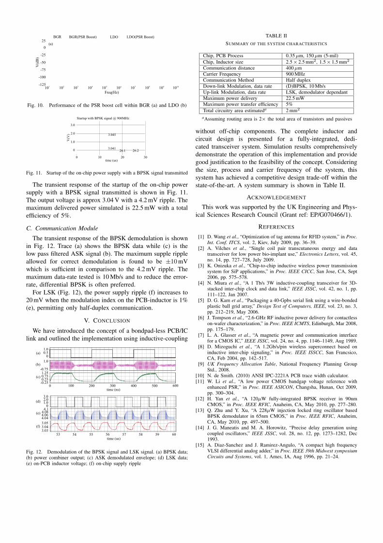
For the rectifier, with (W/L)P1,P2 = 400, Vdrop=1.1 V wasobserved (Fig. 9). The PSR boost cell shows about 30 dBimprovement for the BGR and LDO (Fig. 10).
Input to the rectifierOutput from the rectifier
Vdrop
10.0
5.0
0
-5.0
-10.00 1 2 3 4 5
V(V
)
8
6
4
2
01.10 1.20 1.30 1.40
time (ns)
Fig. 9. Simulation results of the rectifier
BGR BGR(PSR Boost) LDO LDO(PSR Boost)
(a)
V(d
B)
Freq(Hz)
1 2 3 4 5 6 7 8 9 1010 10 10 10 10 10 10 10 10 10-125
-100
-75
-50
-25
0
25
Fig. 10. Performance of the PSR boost cell within BGR (a) and LDO (b)
Startup with BPSK signal @ 900MHz
V(V
)
0
1.0
2.0
3.0
0time (us)
10 20 30
3.045
3.04126.1 26.2
Fig. 11. Startup of the on-chip power supply with a BPSK signal transmitted
The transient response of the startup of the on-chip powersupply with a BPSK signal transmitted is shown in Fig. 11.The output voltage is approx 3.04 V with a 4.2 mV ripple. Themaximum delivered power simulated is 22.5 mW with a totalefficiency of 5%.
C. Communication Module
The transient response of the BPSK demodulation is shownin Fig. 12. Trace (a) shows the BPSK data while (c) is thelow pass filtered ASK signal (b). The maximum supple rippleallowed for correct demodulation is found to be ±10 mVwhich is sufficient in comparison to the 4.2 mV ripple. Themaximum data-rate tested is 10 Mb/s and to reduce the error-rate, differential BPSK is often preferred.
For LSK (Fig. 12), the power supply ripple (f) increases to20 mV when the modulation index on the PCB-inductor is 1%(e), permitting only half-duplex communication.
V. CONCLUSION
We have introduced the concept of a bondpad-less PCB/IClink and outlined the implementation using inductive-coupling
.
(a)
(b)
(c)
(d)
(e)
(f)
1.00.5
01.0
-0.751.250.750.25
-0.250 100 200 300 400 500 600
time (ns)
3.02.01.0
0
53 54 55 56 57 58 59 60time (us)
4.14.084.064.043.053.043.03
Fig. 12. Demodulation of the BPSK signal and LSK signal. (a) BPSK data;(b) power combiner output; (c) ASK demodulated envelope; (d) LSK data;(e) on-PCB inductor voltage; (f) on-chip supply ripple
TABLE IISUMMARY OF THE SYSTEM CHARACTERISTICS
Chip, PCB Process 0.35µm, 150µm (5-mil)Chip, Inductor size 2.5× 2.5 mm2, 1.5× 1.5 mm2
Communication distance 400µmCarrier Frequency 900 MHzCommunication Method Half duplexDown-link Modulation, data rate (D)BPSK, 10 Mb/sUp-link Modulation, data rate LSK, demodulator dependantMaximum power delivery 22.5 mWMaximum power transfer efficiency 5%Total circuitry area estimateda 2 mm2
aAssuming routing area is 2× the total area of transistors and passives
without off-chip components. The complete inductor andcircuit design is presented for a fully-integrated, dedi-cated transceiver system. Simulation results comprehensivelydemonstrate the operation of this implementation and providegood justification to the feasibility of the concept. Consideringthe size, process and carrier frequency of the system, thissystem has achieved a competitive design trade-off within thestate-of-the-art. A system summary is shown in Table II.
ACKNOWLEDGEMENT
This work was supported by the UK Engineering and Phys-ical Sciences Research Council (Grant ref: EP/G070466/1).
REFERENCES
[1] D. Wang et al., “Optimization of tag antenna for RFID system,” in Proc.Int. Conf. ITCS, vol. 2, Kiev, July 2009, pp. 36–39.
[2] A. Vilches et al., “Single coil pair transcutaneous energy and datatransceiver for low power bio-implant use,” Electronics Letters, vol. 45,no. 14, pp. 727–728, July 2009.
[3] K. Onizuka et al., “Chip-to-chip inductive wireless power transmissionsystem for SiP applications,” in Proc. IEEE CICC, San Jose, CA, Sept2006, pp. 575–578.
[4] N. Miura et al., “A 1 Tb/s 3W inductive-coupling transceiver for 3D-stacked inter-chip clock and data link,” IEEE JSSC, vol. 42, no. 1, pp.111–122, Jan 2007.
[5] D. G. Kam et al., “Packaging a 40-Gpbs serial link using a wire-bondedplastic ball grid array,” Design Test of Computers, IEEE, vol. 23, no. 3,pp. 212–219, May 2006.
[6] J. Tompson et al., “2.6-GHz RF inductive power delivery for contactlesson-wafer characterization,” in Proc. IEEE ICMTS, Edinburgh, Mar 2008,pp. 175–179.
[7] L. A. Glasser et al., “A magnetic power and communication interfacefor a CMOS IC,” IEEE JSSC, vol. 24, no. 4, pp. 1146–1149, Aug 1989.
[8] D. Mizoguchi et al., “A 1.2Gb/s/pin wireless superconnect based oninductive inter-chip signaling,” in Proc. IEEE ISSCC, San Francsico,CA, Feb 2004, pp. 142–517.
[9] UK Frequency Allocation Table, National Frequency Planning GroupStd., 2008.
[10] N. de Smith. (2010) ANSI IPC-2221A PCB trace width calculator.[11] W. Li et al., “A low power CMOS bandgap voltage reference with
enhanced PSR,” in Proc. IEEE ASICON, Changsha, Hunan, Oct 2009,pp. 300–304.
[12] H. Yan et al., “A 120µW fully-integrated BPSK receiver in 90nmCMOS,” in Proc. IEEE RFIC, Anaheim, CA, May 2010, pp. 277–280.
[13] Q. Zhu and Y. Xu, “A 228µW injection locked ring oscillator basedBPSK demodulator in 65nm CMOS,” in Proc. IEEE RFIC, Anaheim,CA, May 2010, pp. 497–500.
[14] J. G. Maneatis and M. A. Horowitz, “Precise delay generation usingcoupled oscillators,” IEEE JSSC, vol. 28, no. 12, pp. 1273–1282, Dec1993.
[15] A. Diaz-Sanchez and J. Ramirez-Angulo, “A compact high frequencyVLSI differential analog adder,” in Proc. IEEE 39th Midwest symposiumCircuits and Systems, vol. 1, Ames, IA, Aug 1996, pp. 21–24.