Towards 100 channel dense wavelength division …emerald.ucsd.edu/Docs/Tan2014.pdfTowards 100...
8
Towards 100 channel dense wavelength division multiplexing with 100GHz spacing on silicon D. T. H. Tan, 1,* A. Grieco, 2 and Y. Fainman 2 1 Pillar of Engineering Product Development, Singapore University of Technology and Design, 20 Dover Dr. Singapore 138682, Singapore 2 Electrical and Computer Engineering, University of California San Diego, 9500 Gilman Dr. La Jolla, California 92093, USA * [email protected] Abstract: A 1 by 4 wavelength division multiplexer with 0.5nm bandwidth and no free spectral range limitation is demonstrated on silicon. The device utilizes wide bandwidth filters cascaded with ring resonators in order to select specific ring resonator modes and route each resonant mode to a separate port. This technology will enable dense wavelength division multiplexing covering the C – and L – bands with up to 100 10GB/s channels separated by 100GHz to be implemented for optical interconnects applications. A 1 by 4 wavelength division multiplexer with 3dB channel bandwidths as small as 0.5nm and 1dB insertion loss are demonstrated with 16dB inter-channel crosstalk suppression. A second wavelength division multiplexer scheme with four channels, each spaced 0.5nm apart without any free spectral range limitations is also demonstrated using wide bandwidth filters centered at the same wavelength to select resonances from four different ring resonators with slightly different widths. ©2014 Optical Society of America OCIS codes: (130.7408) Wavelength filtering devices; (130.3120) Integrated optics devices; (130.2790) Guided waves. References and links 1. C. A. Brackett, “Dense wavelength division multiplexing networks: principles and applications,” Selected Areas in Communications, IEEE Journal on 8(948), 964 (1990). 2. A. Mekis, S. Abdalla, D. Foltz, S. Gloeckner, S. Hovey, S. Jackson, Y. Liang, M. Mack, G. Masini, M. Peterson, T. Pinguet, S. Sahni, M. Sharp, P. Sun, D. Tan, L. Verslegers, B. P. Welch, K. Yokoyama, S. Yu, and P. M. De Dobbelaere, “A CMOS photonics platform for high-speed optical interconnects,” in Proceedings of IEEE Photonics Conference, 356 – 357 (2012). 3. S. Assefa, W. M. Green, A. Rylyakov, C. Schow, F. Horst, and Y. Vlasov, “CMOS Integrated Nanophotonics: Enabling Technology for Exascale Computing Systems,” in Optical Fiber Communication Conference/National Fiber Optic Engineers Conference 2011, OSA Technical Digest (CD) (Optical Society of America, 2011), paper OMM6. 4. X. Zheng, F. Y. Liu, J. Lexau, D. Patil, G. Li, Y. Luo, H. D. Thacker, I. Shubin, J. Yao, K. Raj, R. Ho, J. E. Cunningham, and A. V. Krishnamoorthy, “Ultralow power 80 Gb/s arrayed CMOS silicon photonic transceivers for WDM optical links,” J. Lightwave Technol. 30(4), 641–650 (2012). 5. M. Hochberg and T. Baehr-Jones, “Towards fabless silicon photonics,” Nat. Photonics 4(8), 492–494 (2010). 6. F. Li, M. Pelusi, D.-X. Xu, R. Ma, S. Janz, B. J. Eggleton, and D. J. Moss, “All-optical wavelength conversion for 10 Gb/s DPSK signals in a silicon ring resonator,” Opt. Express 19(23), 22410–22416 (2011). 7. L. C. Kimerling, D. Ahn, A. B. Apsel, M. Beals, D. Carothers, Y.-K. Chen, T. Conway, D. M. Gill, M. Grove, C.-Y. Hong, M. Lipson, J. Liu, J. Michel, D. Pan, S. S. Patel, A. T. Pomerene, M. Rasras, D. K. Sparacin, K.-Y. Tu, A. E. White, and C. W. Wong, “Electronic-photonic integrated circuits on the CMOS platform,” Proc. SPIE 6125, 612502 (2006). 8. D. T. H. Tan, K. Ikeda, S. Zamek, A. Mizrahi, M. P. Nezhad, A. V. Krishnamoorthy, K. Raj, J. E. Cunningham, X. Zheng, I. Shubin, Y. Luo, and Y. Fainman, “Wide bandwidth, low loss 1 by 4 wavelength division multiplexer on silicon for optical interconnects,” Opt. Express 19(3), 2401–2409 (2011). 9. S. Kawanishi, H. Takara, K. Uchiyama, I. Shake, and K. Mori, “3 Tbit/s (160 Gbit/s × 19 channel) optical TDM and WDM transmission experiment,” Electron. Lett. 35(10), 826–827 (1999). 10. W. Bogaerts, S. K. Selvaraja, P. Dumon, J. Brouckaert, K. De Vos, D. Van Thourhout, and R. Baets, “Silicon- on-Insulator Spectral Filters Fabricated With CMOS Technology,” IEEE J. Sel. Top. Quantum Electron. 16(1), 33–44 (2010). #207437 - $15.00 USD Received 28 Feb 2014; revised 10 Apr 2014; accepted 14 Apr 2014; published 22 Apr 2014 (C) 2014 OSA 5 May 2014 | Vol. 22, No. 9 | DOI:10.1364/OE.22.010408 | OPTICS EXPRESS 10408
Transcript of Towards 100 channel dense wavelength division …emerald.ucsd.edu/Docs/Tan2014.pdfTowards 100...
Towards 100 channel dense wavelength division multiplexing with 100GHz spacing on silicon
D. T. H. Tan,1,* A. Grieco,2 and Y. Fainman2 1Pillar of Engineering Product Development, Singapore University of Technology and Design, 20 Dover Dr.
Singapore 138682, Singapore 2Electrical and Computer Engineering, University of California San Diego, 9500 Gilman Dr. La Jolla, California
92093, USA *[email protected]
Abstract: A 1 by 4 wavelength division multiplexer with 0.5nm bandwidth and no free spectral range limitation is demonstrated on silicon. The device utilizes wide bandwidth filters cascaded with ring resonators in order to select specific ring resonator modes and route each resonant mode to a separate port. This technology will enable dense wavelength division multiplexing covering the C – and L – bands with up to 100 10GB/s channels separated by 100GHz to be implemented for optical interconnects applications. A 1 by 4 wavelength division multiplexer with 3dB channel bandwidths as small as 0.5nm and 1dB insertion loss are demonstrated with 16dB inter-channel crosstalk suppression. A second wavelength division multiplexer scheme with four channels, each spaced 0.5nm apart without any free spectral range limitations is also demonstrated using wide bandwidth filters centered at the same wavelength to select resonances from four different ring resonators with slightly different widths.
©2014 Optical Society of America
OCIS codes: (130.7408) Wavelength filtering devices; (130.3120) Integrated optics devices; (130.2790) Guided waves.
References and links
1. C. A. Brackett, “Dense wavelength division multiplexing networks: principles and applications,” Selected Areas in Communications, IEEE Journal on 8(948), 964 (1990).
2. A. Mekis, S. Abdalla, D. Foltz, S. Gloeckner, S. Hovey, S. Jackson, Y. Liang, M. Mack, G. Masini, M. Peterson, T. Pinguet, S. Sahni, M. Sharp, P. Sun, D. Tan, L. Verslegers, B. P. Welch, K. Yokoyama, S. Yu, and P. M. De Dobbelaere, “A CMOS photonics platform for high-speed optical interconnects,” in Proceedings of IEEE Photonics Conference, 356 – 357 (2012).
3. S. Assefa, W. M. Green, A. Rylyakov, C. Schow, F. Horst, and Y. Vlasov, “CMOS Integrated Nanophotonics: Enabling Technology for Exascale Computing Systems,” in Optical Fiber Communication Conference/National Fiber Optic Engineers Conference 2011, OSA Technical Digest (CD) (Optical Society of America, 2011), paper OMM6.
4. X. Zheng, F. Y. Liu, J. Lexau, D. Patil, G. Li, Y. Luo, H. D. Thacker, I. Shubin, J. Yao, K. Raj, R. Ho, J. E. Cunningham, and A. V. Krishnamoorthy, “Ultralow power 80 Gb/s arrayed CMOS silicon photonic transceivers for WDM optical links,” J. Lightwave Technol. 30(4), 641–650 (2012).
5. M. Hochberg and T. Baehr-Jones, “Towards fabless silicon photonics,” Nat. Photonics 4(8), 492–494 (2010). 6. F. Li, M. Pelusi, D.-X. Xu, R. Ma, S. Janz, B. J. Eggleton, and D. J. Moss, “All-optical wavelength conversion
for 10 Gb/s DPSK signals in a silicon ring resonator,” Opt. Express 19(23), 22410–22416 (2011). 7. L. C. Kimerling, D. Ahn, A. B. Apsel, M. Beals, D. Carothers, Y.-K. Chen, T. Conway, D. M. Gill, M. Grove,
C.-Y. Hong, M. Lipson, J. Liu, J. Michel, D. Pan, S. S. Patel, A. T. Pomerene, M. Rasras, D. K. Sparacin, K.-Y. Tu, A. E. White, and C. W. Wong, “Electronic-photonic integrated circuits on the CMOS platform,” Proc. SPIE 6125, 612502 (2006).
8. D. T. H. Tan, K. Ikeda, S. Zamek, A. Mizrahi, M. P. Nezhad, A. V. Krishnamoorthy, K. Raj, J. E. Cunningham, X. Zheng, I. Shubin, Y. Luo, and Y. Fainman, “Wide bandwidth, low loss 1 by 4 wavelength division multiplexer on silicon for optical interconnects,” Opt. Express 19(3), 2401–2409 (2011).
9. S. Kawanishi, H. Takara, K. Uchiyama, I. Shake, and K. Mori, “3 Tbit/s (160 Gbit/s × 19 channel) optical TDM and WDM transmission experiment,” Electron. Lett. 35(10), 826–827 (1999).
10. W. Bogaerts, S. K. Selvaraja, P. Dumon, J. Brouckaert, K. De Vos, D. Van Thourhout, and R. Baets, “Silicon-on-Insulator Spectral Filters Fabricated With CMOS Technology,” IEEE J. Sel. Top. Quantum Electron. 16(1), 33–44 (2010).
#207437 - $15.00 USD Received 28 Feb 2014; revised 10 Apr 2014; accepted 14 Apr 2014; published 22 Apr 2014(C) 2014 OSA 5 May 2014 | Vol. 22, No. 9 | DOI:10.1364/OE.22.010408 | OPTICS EXPRESS 10408
11. D. T. H. Tan, P. C. Sun, and Y. Fainman, “Monolithic nonlinear pulse compressor on a silicon chip,” Nat Commun 1(8), 116 (2010).
12. D. T. H. Tan, “Optical pulse compression on a silicon chip – Effect of group velocity dispersion and free carriers,” Appl. Phys. Lett. 101(21), 211112 (2012).
13. G. F. R. Chen, T. Wang, C. Donnelly, and D. T. H. Tan, “Second and third order dispersion generation using nonlinearly chirped silicon waveguide gratings,” Opt. Express 21(24), 29223–29230 (2013).
14. D. T. H. Tan, K. Ikeda, and Y. Fainman, “Coupled chirped vertical gratings for on chip group velocity dispersion engineering,” Appl. Phys. Lett. 95(14), 141109 (2009).
15. D. T. H. Tan, K. Ikeda, R. E. Saperstein, B. Slutsky, and Y. Fainman, “Chip-scale dispersion engineering using chirped vertical gratings,” Opt. Lett. 33(24), 3013–3015 (2008).
16. W. Shi, H. Yun, C. Lin, J. Flueckiger, N. A. F. Jaeger, and L. Chrostowski, “Coupler-apodized Bragg-grating add-drop filter,” Opt. Lett. 38(16), 3068–3070 (2013).
17. W. Shi, X. Wang, W. Zhang, L. Chrostowski, and N. A. F. Jaeger, “Contradirectional couplers in silicon-on-insulator rib waveguides,” Opt. Lett. 36(20), 3999–4001 (2011).
18. W. Shi, X. Wang, W. Zhang, H. Yun, C. Lin, L. Chrostowski, and N. A. F. Jaeger, “Grating-coupled silicon microring resonators,” Appl. Phys. Lett. 100(12), 121118 (2012).
19. R. Boeck, W. Shi, L. Chrostowski, and N. A. F. Jaeger, “FSR-Eliminated Vernier Racetrack Resonators Using Grating-Assisted Couplers,” IEEE Photonics Journal 5(5), 2202511 (2013).
20. W. Bogaerts, P. De Heyn, T. Van Vaerenbergh, K. De Vos, S. Kumar Selvaraja, T. Claes, P. Dumon, P. Bienstman, D. Van Thourhout, and R. Baets, “Silicon microring resonators,” Laser Photonics Rev. 6(1), 47–73 (2012).
21. A. Yariv and P. Yeh, Optical Waves in Crystals: Propagation and Control of Laser Radiation (Wiley, 2002). 22. W. Shi, H. Yun, C. Lin, M. Greenberg, X. Wang, Y. Wang, S. T. Fard, J. Flueckiger, N. A. F. Jaeger, and L.
Chrostowski, “Ultra-compact, flat-top demultiplexer using anti-reflection contra-directional couplers for CWDM networks on silicon,” Opt. Express 21(6), 6733–6738 (2013).
23. F. Xia, M. Rooks, L. Sekaric, and Y. Vlasov, “Ultra-compact high order ring resonator filters using submicron silicon photonic wires for on-chip optical interconnects,” Opt. Express 15(19), 11934–11941 (2007).
24. J. E. Cunningham, I. Shubin, X. Zheng, T. Pinguet, A. Mekis, Y. Luo, H. Thacker, G. Li, J. Yao, K. Raj, and A. V. Krishnamoorthy, “Highly-efficient thermally-tuned resonant optical filters,” Opt. Express 18(18), 19055–19063 (2010).
1. Introduction
Wavelength division multiplexing (WDM) is a commonly used technique in fiber optic communication systems to increase the aggregate transmission bandwidth [1]. Dense WDM (DWDM) are standardized such that channels are spaced by 100GHz, for a total of 50 channels within the C – band (spanning 1530nm – 1570nm), or spaced by 50GHz, for a total of 100 possible channels within the C – band. With the inclusion of the L – band, the number of possible channels for 100GHz and 50GHz channel spacing may be increased to 100 and 200 respectively. With the recent advances in Si-photonics and interest from the computing industry [2–4], old paradigms in fiber optics are now being exploited for CMOS compatible integration of optical interconnects and networking with computing systems [5–7]. To further augment the data capacity of optical interconnects, WDM can be used to create multiple channels within the C- and L- bands. We previously demonstrated a low loss, wide bandwidth 1 by 4 wavelength division multiplexer on silicon [8]. The advantage of the large bandwidth was the greater resistance to fabrication errors and temperature fluctuations, and the ability to accommodate data with more spectral content within a single channel, for example to combine optical time division multiplexing (OTDM) signals within each WDM channel to achieve Tb/s system capacities with fewer WDM channels [9].
However, due to the complexity in OTDM demultiplexing, there is a practical benefit from exploiting the available optical carrier bandwidth using purely WDM techniques with a moderate bandwidth per channel (e.g. spacing at 50 or 100 GHz). For realization of the DWDM concept on a chip, one of the essential components is a multiplexing/demultiplexing filter. Several approaches for implementing this functionality have been investigated including ring resonators, arrayed waveguide gratings and coupled vertical gratings, each with their relative merits and drawbacks. Ring resonators have multiple resonant modes, spaced by a corresponding free spectral range which limits the total bandwidth useable for WDM. Arrayed waveguide gratings [10] may be designed to have larger free spectral ranges than that typical in ring resonators, but have larger footprints, and are less easily integrated with other photonic lightwave circuit components, including microheaters for thermal tuning, compared to ring resonators and coupled gratings. Previous work utilizing coupled vertical gratings had
#207437 - $15.00 USD Received 28 Feb 2014; revised 10 Apr 2014; accepted 14 Apr 2014; published 22 Apr 2014(C) 2014 OSA 5 May 2014 | Vol. 22, No. 9 | DOI:10.1364/OE.22.010408 | OPTICS EXPRESS 10409
applications in pulse compression [11, 12], dispersion engineering [13–15] and WDM [8, 16–19]. In contrast to ring resonators which have multiple resonant modes spaced by a corresponding free spectral range, coupled grating devices possess only a single resonance. Consequently, the bandwidth utilization of the latter is not limited by any associated free spectral range. However, the drawback of the coupled grating device technology is the large channel bandwidth. The previously demonstrated 3nm bandwidth [8] implies that only around 30 WDM channels may be accommodated across the C – and L – bands, and for full 3 nm bandwidth utilization, a speed of electronic detection which is currently unrealistic will be required. To overcome these limitations, we propose to combine the advantages of both the ring resonator based filters (sufficiently small bandwidth to achieve 100GHz channel spacing for DWDM), and the coupled vertical grating filters (no free spectral range limitation). In this manuscript we demonstrate an integrated 1 by 4 WDM device using these techniques, with channel bandwidths as small as 0.5nm, 1dB loss and 16dB inter-channel crosstalk suppression.
2. Device design
A schematic diagram of the proposed device is illustrated in Fig. 1(a). We adopt a silicon on insulator (SOI) platform with 250nm Si device layer and SiO2 over- and under- cladding. The device is comprised of a ring resonator whose output is transmitted to a 1 by 4 WDM demultiplexer based on a coupled vertical grating device with a coupling gap, G = 80nm. Here, we design a 1 by 4 WDM device based on coupled vertical gratings so as to meet a channel spacing of 6.5nm. Each grating in the device is apodized [8] to minimize ripple in the transmission spectrum. Design principles for the coupled grating add/drop filters are detailed in Ref. 8. In addition, the calculated effective index vs. grating width is shown in Fig. 1(b). The four drop port wavelengths are further designed to be centered at 1554nm, 1560.5nm, 1567nm, 1573.5nm (6.5nm channel spacing) by using slightly different values of W1, W2, W3 and W4 [8]. The measured spectral response of the 1 by 4 WDM (device segment highlighted within the grey dotted rectangle in Fig. 1(a)). is shown in Fig. 1(c). In order to minimize the footprint and complexity of the mode selector, we design the ring resonator to have a free spectral range of 6.5 nm, coincident with each of the four drop port wavelengths of the 1 by 4 WDM demultiplexer such that four resonant modes from the ring resonator filter may be routed out of each of the four output ports of the coupled vertical grating filters.
The free spectral range of a ring resonator is given by the following
expression,2
FSR .gn Lλ= , where λ is the wavelength of the resonance, ng is the group index
of the waveguide and L is the circumference of the ring [20]. The location of the mth resonance associated with the ring resonator is given by, eff. . ( )m L nλ λ= (Eq. (1), where neff is the effective index of the waveguide. The effective index as a function of waveguide width is calculated and shown in Fig. 1(b). The width of the waveguide forming the ring resonator is set at 0.40µm. To meet the requirements of the 6.5nm FSR, the ring was designed to have an optical path length of 83µm.
#207437 - $15.00 USD Received 28 Feb 2014; revised 10 Apr 2014; accepted 14 Apr 2014; published 22 Apr 2014(C) 2014 OSA 5 May 2014 | Vol. 22, No. 9 | DOI:10.1364/OE.22.010408 | OPTICS EXPRESS 10410
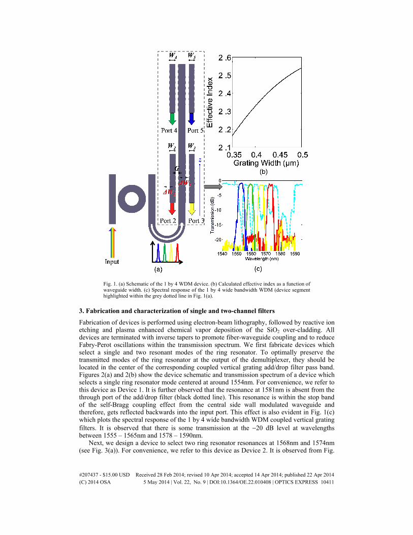
Fig. 1. (a) Schematic of the 1 by 4 WDM device. (b) Calculated effective index as a function of waveguide width. (c) Spectral response of the 1 by 4 wide bandwidth WDM (device segment highlighted within the grey dotted line in Fig. 1(a).
3. Fabrication and characterization of single and two-channel filters
Fabrication of devices is performed using electron-beam lithography, followed by reactive ion etching and plasma enhanced chemical vapor deposition of the SiO2 over-cladding. All devices are terminated with inverse tapers to promote fiber-waveguide coupling and to reduce Fabry-Perot oscillations within the transmission spectrum. We first fabricate devices which select a single and two resonant modes of the ring resonator. To optimally preserve the transmitted modes of the ring resonator at the output of the demultiplexer, they should be located in the center of the corresponding coupled vertical grating add/drop filter pass band. Figures 2(a) and 2(b) show the device schematic and transmission spectrum of a device which selects a single ring resonator mode centered at around 1554nm. For convenience, we refer to this device as Device 1. It is further observed that the resonance at 1581nm is absent from the through port of the add/drop filter (black dotted line). This resonance is within the stop band of the self-Bragg coupling effect from the central side wall modulated waveguide and therefore, gets reflected backwards into the input port. This effect is also evident in Fig. 1(c) which plots the spectral response of the 1 by 4 wide bandwidth WDM coupled vertical grating filters. It is observed that there is some transmission at the −20 dB level at wavelengths between 1555 – 1565nm and 1578 – 1590nm.
Next, we design a device to select two ring resonator resonances at 1568nm and 1574nm (see Fig. 3(a)). For convenience, we refer to this device as Device 2. It is observed from Fig.
#207437 - $15.00 USD Received 28 Feb 2014; revised 10 Apr 2014; accepted 14 Apr 2014; published 22 Apr 2014(C) 2014 OSA 5 May 2014 | Vol. 22, No. 9 | DOI:10.1364/OE.22.010408 | OPTICS EXPRESS 10411
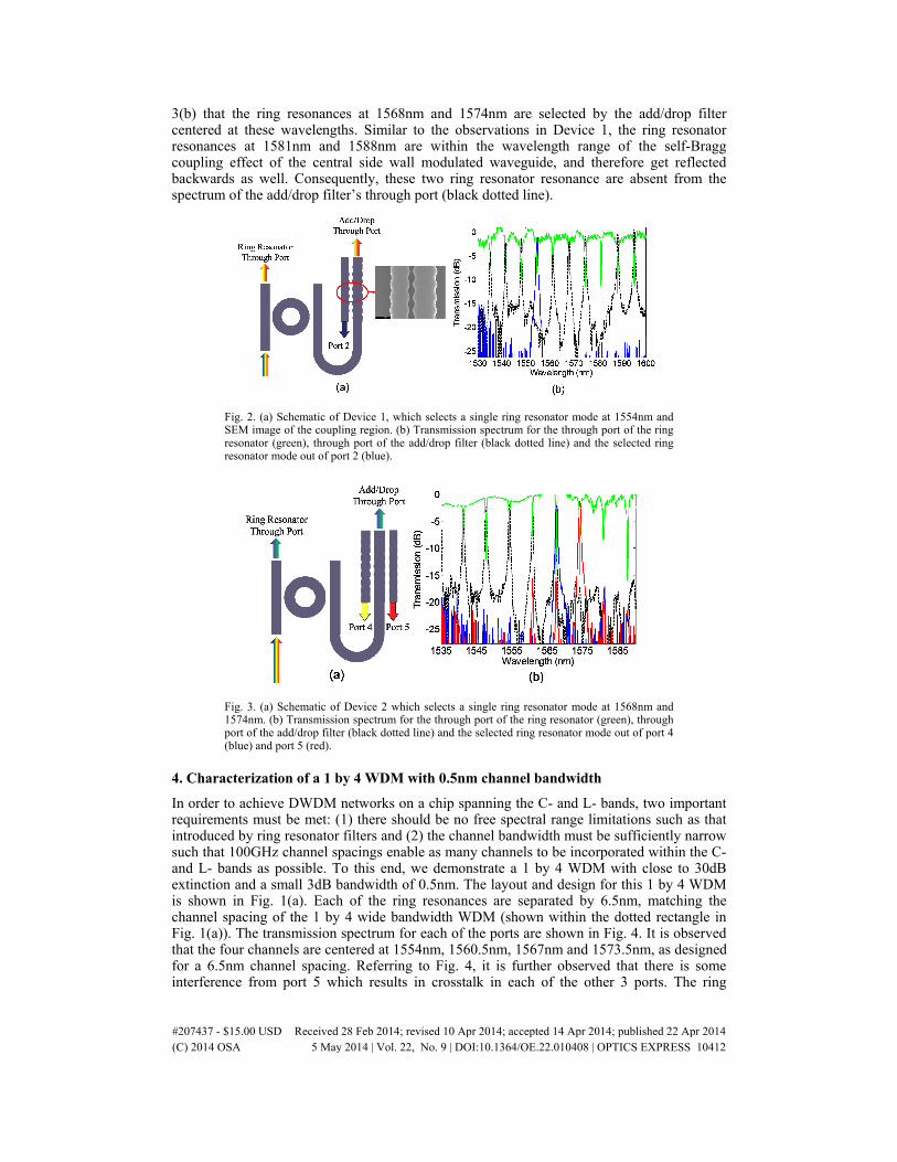
3(b) that the ring resonances at 1568nm and 1574nm are selected by the add/drop filter centered at these wavelengths. Similar to the observations in Device 1, the ring resonator resonances at 1581nm and 1588nm are within the wavelength range of the self-Bragg coupling effect of the central side wall modulated waveguide, and therefore get reflected backwards as well. Consequently, these two ring resonator resonance are absent from the spectrum of the add/drop filter’s through port (black dotted line).
Fig. 2. (a) Schematic of Device 1, which selects a single ring resonator mode at 1554nm and SEM image of the coupling region. (b) Transmission spectrum for the through port of the ring resonator (green), through port of the add/drop filter (black dotted line) and the selected ring resonator mode out of port 2 (blue).
Fig. 3. (a) Schematic of Device 2 which selects a single ring resonator mode at 1568nm and 1574nm. (b) Transmission spectrum for the through port of the ring resonator (green), through port of the add/drop filter (black dotted line) and the selected ring resonator mode out of port 4 (blue) and port 5 (red).
4. Characterization of a 1 by 4 WDM with 0.5nm channel bandwidth
In order to achieve DWDM networks on a chip spanning the C- and L- bands, two important requirements must be met: (1) there should be no free spectral range limitations such as that introduced by ring resonator filters and (2) the channel bandwidth must be sufficiently narrow such that 100GHz channel spacings enable as many channels to be incorporated within the C- and L- bands as possible. To this end, we demonstrate a 1 by 4 WDM with close to 30dB extinction and a small 3dB bandwidth of 0.5nm. The layout and design for this 1 by 4 WDM is shown in Fig. 1(a). Each of the ring resonances are separated by 6.5nm, matching the channel spacing of the 1 by 4 wide bandwidth WDM (shown within the dotted rectangle in Fig. 1(a)). The transmission spectrum for each of the ports are shown in Fig. 4. It is observed that the four channels are centered at 1554nm, 1560.5nm, 1567nm and 1573.5nm, as designed for a 6.5nm channel spacing. Referring to Fig. 4, it is further observed that there is some interference from port 5 which results in crosstalk in each of the other 3 ports. The ring
#207437 - $15.00 USD Received 28 Feb 2014; revised 10 Apr 2014; accepted 14 Apr 2014; published 22 Apr 2014(C) 2014 OSA 5 May 2014 | Vol. 22, No. 9 | DOI:10.1364/OE.22.010408 | OPTICS EXPRESS 10412
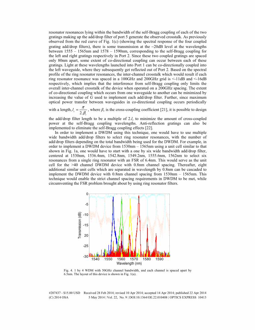
resonator resonances lying within the bandwidth of the self-Bragg coupling of each of the two gratings making up the add/drop filter of port 5 generate the observed crosstalk. As previously observed from the red curve of Fig. 1(c) (showing the spectral response of the four coupled grating add/drop filters), there is some transmission at the −20dB level at the wavelengths between 1555 – 1565nm and 1578 – 1590nm, corresponding to the self-Bragg coupling for the left and right gratings respectively in Port 2. Since these two coupled gratings are spaced only 80nm apart, some extent of co-directional coupling can occur between each of these gratings. Light at these wavelengths launched into Port 1 can be co-directionally coupled into the left waveguide, where they subsequently get reflected out of Port 2. Based on the spectral profile of the ring resonator resonances, the inter-channel crosstalk which would result if each ring resonator resonance was spaced in a 100GHz and 200GHz grid is <-11dB and <-16dB respectively, which implies that the interference from self-Bragg coupling only limits the overall inter-channel crosstalk of the device when operated on a 200GHz spacing. The extent of co-directional coupling which occurs from one waveguide to another can be minimized by increasing the value of G used to implement each add/drop filter. Further, since maximum optical power transfer between waveguides in co-directional coupling occurs periodically
with a length,2.c
c
lπβ
= , where βc is the cross-coupling coefficient [21], it is possible to design
the add/drop filter length to be a multiple of 2.lc to minimize the amount of cross-coupled power at the self-Bragg coupling wavelengths. Anti-reflection gratings can also be implemented to eliminate the self-Bragg coupling effects [22].
In order to implement a DWDM using this technique, one would have to use multiple wide bandwidth add/drop filters to select ring resonator resonances, with the number of add/drop filters depending on the total bandwidth being used for the DWDM. For example, in order to implement a DWDM device from 1530nm – 1565nm using a unit cell similar to that shown in Fig. 1a, one would have to start with a one by six wide bandwidth add/drop filter, centered at 1530nm, 1536.4nm, 1542.8nm, 1549.2nm, 1555.6nm, 1562nm to select six resonances from a single ring resonator with an FSR of 6.4nm. This would serve as the unit cell for the >40 channel DWDM device with 0.8nm channel spacing. Thereafter, eight additional similar unit cells which are separated in wavelength by 0.8nm can be cascaded to implement the DWDM device with 0.8nm channel spacing from 1530nm – 1565nm. This technique would enable the strict channel spacing requirements in DWDM to be met, while circumventing the FSR problem brought about by using ring resonator filters.
1540 1550 1560 1570 1580 1590-30
-25
20
-15
-10
-5
0
Wavelength (nm)
Tran
smis
sion
(dB)
Fig. 4. 1 by 4 WDM with 50GHz channel bandwidth, and each channel is spaced apart by 6.5nm. The layout of this device is shown in Fig. 1(a).
#207437 - $15.00 USD Received 28 Feb 2014; revised 10 Apr 2014; accepted 14 Apr 2014; published 22 Apr 2014(C) 2014 OSA 5 May 2014 | Vol. 22, No. 9 | DOI:10.1364/OE.22.010408 | OPTICS EXPRESS 10413
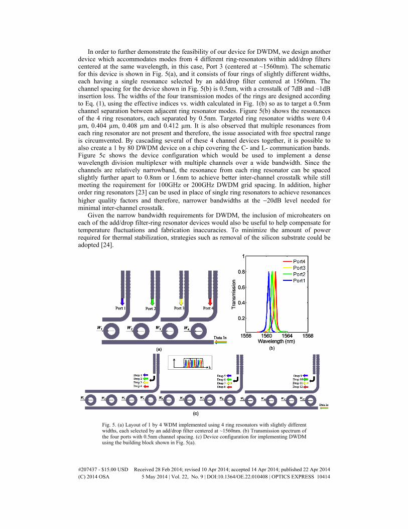
In order to further demonstrate the feasibility of our device for DWDM, we design another device which accommodates modes from 4 different ring-resonators within add/drop filters centered at the same wavelength, in this case, Port 3 (centered at ~1560nm). The schematic for this device is shown in Fig. 5(a), and it consists of four rings of slightly different widths, each having a single resonance selected by an add/drop filter centered at 1560nm. The channel spacing for the device shown in Fig. 5(b) is 0.5nm, with a crosstalk of 7dB and ~1dB insertion loss. The widths of the four transmission modes of the rings are designed according to Eq. (1), using the effective indices vs. width calculated in Fig. 1(b) so as to target a 0.5nm channel separation between adjacent ring resonator modes. Figure 5(b) shows the resonances of the 4 ring resonators, each separated by 0.5nm. Targeted ring resonator widths were 0.4 µm, 0.404 µm, 0.408 µm and 0.412 µm. It is also observed that multiple resonances from each ring resonator are not present and therefore, the issue associated with free spectral range is circumvented. By cascading several of these 4 channel devices together, it is possible to also create a 1 by 80 DWDM device on a chip covering the C- and L- communication bands. Figure 5c shows the device configuration which would be used to implement a dense wavelength division multiplexer with multiple channels over a wide bandwidth. Since the channels are relatively narrowband, the resonance from each ring resonator can be spaced slightly further apart to 0.8nm or 1.6nm to achieve better inter-channel crosstalk while still meeting the requirement for 100GHz or 200GHz DWDM grid spacing. In addition, higher order ring resonators [23] can be used in place of single ring resonators to achieve resonances higher quality factors and therefore, narrower bandwidths at the −20dB level needed for minimal inter-channel crosstalk.
Given the narrow bandwidth requirements for DWDM, the inclusion of microheaters on each of the add/drop filter-ring resonator devices would also be useful to help compensate for temperature fluctuations and fabrication inaccuracies. To minimize the amount of power required for thermal stabilization, strategies such as removal of the silicon substrate could be adopted [24].
Fig. 5. (a) Layout of 1 by 4 WDM implemented using 4 ring resonators with slightly different widths, each selected by an add/drop filter centered at ~1560nm. (b) Transmission spectrum of the four ports with 0.5nm channel spacing. (c) Device configuration for implementing DWDM using the building block shown in Fig. 5(a).
#207437 - $15.00 USD Received 28 Feb 2014; revised 10 Apr 2014; accepted 14 Apr 2014; published 22 Apr 2014(C) 2014 OSA 5 May 2014 | Vol. 22, No. 9 | DOI:10.1364/OE.22.010408 | OPTICS EXPRESS 10414
4. Conclusions
In this paper, we have demonstrated 1 by 4 WDM devices which have the potential to be implemented for 80-channel DWDM on-chip systems on a 100GHz or 200GHz grid spanning the C – and L – bands. Two different approaches are demonstrated. First, four ring resonator modes from a single ring resonator with its FSR matching the channel spacing of a wider bandwidth 1 by 4 WDM system is designed and characterized to have 16dB cross talk suppression, 6.5nm channel spacing and 0.5nm channel bandwidth. The second approach which we demonstrated involves using the add/drop filter located at the same wavelength to select a single resonance from four different ring resonators with slightly different widths, so as to achieve a channel spacing of 0.5nm. By cascading multiple devices, either of these two approaches may be used to implement an 80 channel DWDM device on silicon. This system would enable optical interconnects with ultra-high data capacity to be implemented for applications in data centers and microprocessors.
Acknowledgments
This work was supported by the SUTD-MIT International Design Center, the SUTD-ZJU collaborative research grant, the MOE ACRF Tier 2 research grant, the NSF MRI, the NSF CIAN ERC, and the ONR MURI program.
#207437 - $15.00 USD Received 28 Feb 2014; revised 10 Apr 2014; accepted 14 Apr 2014; published 22 Apr 2014(C) 2014 OSA 5 May 2014 | Vol. 22, No. 9 | DOI:10.1364/OE.22.010408 | OPTICS EXPRESS 10415