Topological photonics and polaritonics
43
Topological photonics and polaritonics 1 Alexander Khanikaev 1,2 1 Department of Electrical Engineering and Department of Physics, The City College of New York, NY, USA 2 Department of Physics, The City College and the Graduate Center of CUNY, NY, USA PhD students and postdocs: Xiang Ni, Sriram Guddala, Filipp Komisasrenko, Mengyao Li, Matthew Weiner, Kai Chen, Anton Vakulenko, Svetlana Kiriushechkina, Yuma Kawaguchi Collaborators: Andrea Alù, Yuri Kivshar, Vinod Menon, Dmitriy Kryzhanovskiy, Anton Samusev TEXAS TECH University, 23 March 2021.
Transcript of Topological photonics and polaritonics

Topological photonics and polaritonics
1
Alexander Khanikaev1,2
1 Department of Electrical Engineering and Department of Physics,
The City College of New York, NY, USA2Department of Physics, The City College and the Graduate Center of CUNY, NY, USA
PhD students and postdocs: Xiang Ni, Sriram Guddala, Filipp Komisasrenko, Mengyao Li, Matthew Weiner, Kai Chen, Anton Vakulenko, Svetlana Kiriushechkina, Yuma Kawaguchi
Collaborators: Andrea Alù, Yuri Kivshar, Vinod Menon, Dmitriy Kryzhanovskiy, Anton Samusev
TEXAS TECH University, 23 March 2021.
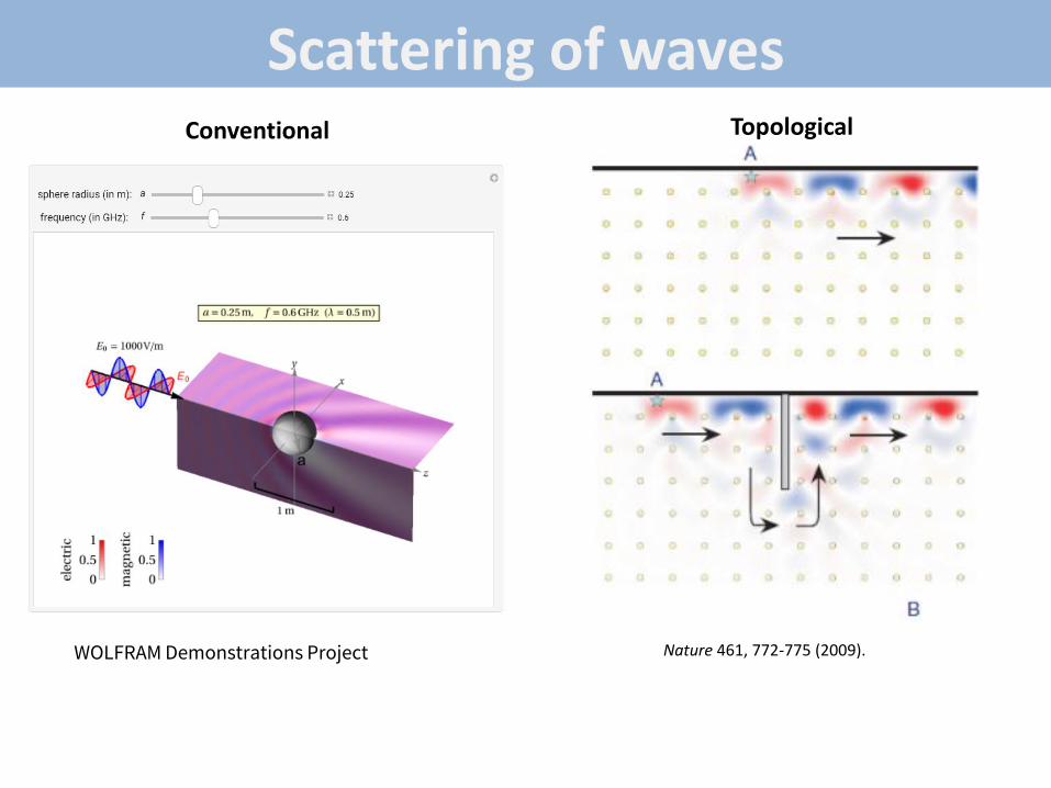
Scattering of waves
WOLFRAM Demonstrations Project
Conventional Topological
Nature 461, 772-775 (2009).
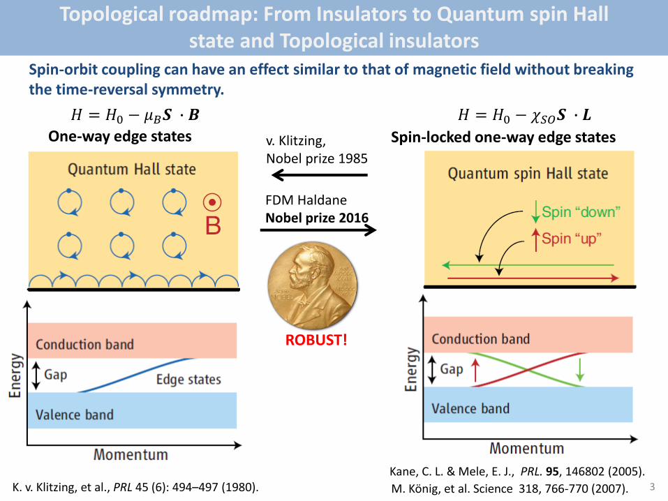
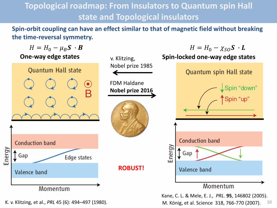
Topological roadmap: From Insulators to Quantum spin Hall state and Topological insulators
3
One-way edge states Spin-locked one-way edge states
Kane, C. L. & Mele, E. J., PRL. 95, 146802 (2005).
Spin-orbit coupling can have an effect similar to that of magnetic field without breaking the time-reversal symmetry.
𝐻 = 𝐻0 − 𝜇𝐵𝑺 ∙ 𝑩 𝐻 = 𝐻0 − 𝜒𝑆𝑂𝑺 ∙ 𝑳
ROBUST!
FDM HaldaneNobel prize 2016
v. Klitzing, Nobel prize 1985
M. König, et al. Science 318, 766-770 (2007).K. v. Klitzing, et al., PRL 45 (6): 494–497 (1980).

From condensed matter to photonics:photonic crystals – semiconductors of light
4
Joannopoulos, J. D., Johnson, S. G., Winn, J. N. & Meade, R. D., Photonic Crystals: Molding the Flow of Light, 2nd ed. (Princeton University Press, Princeton , 2008).
Periodically stacking materials with different dielectric or magnetic properties
Infinite in all other directions

Topological order for photons
Classification of photonic topological systems
+Non-Hermitian (parity-time) + unconventional symmetries (supersymmetry/square root)?
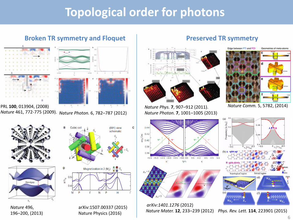
Topological order for photons
6
Nature Phys. 7, 907–912 (2011).Nature Photon. 7, 1001–1005 (2013)
arXiv:1507.00337 (2015)Nature Physics (2016)
Nature Photon. 6, 782–787 (2012)
Nature Mater. 12, 233–239 (2012)Nature 496, 196–200, (2013)
Nature 461, 772-775 (2009).
Nature Comm. 5, 5782, (2014)
Phys. Rev. Lett. 114, 223901 (2015)arXiv:1401.1276 (2012)
Broken TR symmetry and Floquet Preserved TR symmetry
PRL 100, 013904, (2008)

Topological invariants for photonicsMathematical foundation of topological photonics & Schrodinger form of Maxwell’s equations.
𝐻-effective Hamiltonian
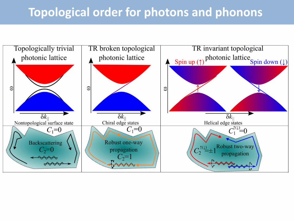
Topological order for photons and phonons

Effective Hamiltonian Description
+ ]𝑬𝒅 =[ 𝑬𝒅
𝒜 𝐤 = ⟨𝑬𝒅 𝐫 𝛻𝑘 𝑬𝒅⟩
𝐶 =1
2𝜋𝑖න
BZ
𝑑2𝑘 𝛻𝑘 ×𝒜 𝑧 =12
𝑯𝟎||z
K
𝐶 = 𝐶K + 𝐶K′ = 1
Haldane, Raghu, PRL 100, 013904, (2008)
Topological roadmap: From Insulators to Quantum spin Hall state and Topological insulators
10
One-way edge states Spin-locked one-way edge states
Kane, C. L. & Mele, E. J., PRL. 95, 146802 (2005).
Spin-orbit coupling can have an effect similar to that of magnetic field without breaking the time-reversal symmetry.
𝐻 = 𝐻0 − 𝜇𝐵𝑺 ∙ 𝑩 𝐻 = 𝐻0 − 𝜒𝑆𝑂𝑺 ∙ 𝑳
ROBUST!
FDM HaldaneNobel prize 2016
v. Klitzing, Nobel prize 1985
M. König, et al. Science 318, 766-770 (2007).K. v. Klitzing, et al., PRL 45 (6): 494–497 (1980).

Role of Symmetries: topological systems with the time-reversal symmetry
ℋ = ℋ0 + 𝑉𝑆𝑂
Preserved TR symmetry ensures the presence of Kramer’s TR partners (two spins/helicities) in fermionic systems but not in bosonic.
𝒯𝑓 ℋ 𝒯𝑓−1 = ℋ and 𝒯𝑓
2 = −1
ℋ0 - unperturbed fermionic lattice potential
𝑉𝑆𝑂 = −𝜒𝑆𝑂𝑺 ∙ 𝑳 - gauge (SO) potential inducing topological transition (band crossing)
Kane, C. L. & Mele, E. J., Phys. Rev. Lett. 95, 146802 (2005).Hasan, M. Z. & Kane, C. L., Rev. Mod. Phys. 82, 3045-3067 (2010).Qi, X.-L. & Zhang, S.-C., Rev. Mod. Phys. 83, 1057-1110 (2011).
𝒯𝑏 ℋ 𝒯𝑏−1 = ℋ and 𝒯𝑏
2 = 1
Fermions Classical/Bosons ℋ = ℋ0 + 𝑉𝑔𝑎𝑢𝑔𝑒
ℋ0 - unperturbed bosonic lattice potential
𝑉𝑔𝑎𝑢𝑔𝑒 =Photonic “gauge” potential
(SO or pseudo-magnetic) inducing topological transition
Consequence: TR alone is not sufficient for topological order for bosons, i.e. no topological phase analogous to fermionic TR phase is possible.
Robustness is insured by TR symmetry (no magnetic defects are allowed). Doublets generated by TR are locked to theirpropagation directions – spin-locking.
Solution: non-TR symmetry protected phases.
መ𝐶𝑏 ℋ መ𝐶𝑏−1 = ℋ and መ𝐶𝑏
2 = −1
Where መ𝐶𝑏 is a spatial or internal symmetry operator generating a doublet state –pseudo-spin degree of freedom.
𝒯𝑏𝜓↑ ↓ 𝒌 = 𝒯𝑏𝜓
↓ ↑ −𝒌
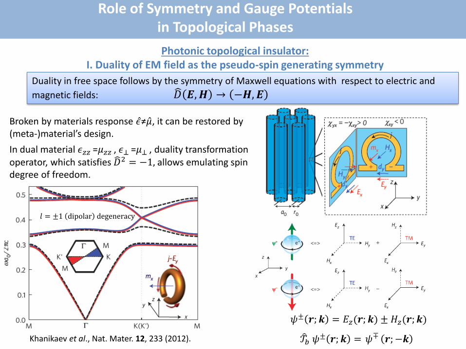
Role of Symmetry and Gauge Potentials in Topological Phases
Photonic topological insulator: I. Duality of EM field as the pseudo-spin generating symmetry
𝜓± 𝒓; 𝒌 = 𝐸𝑧(𝒓; 𝒌) ± 𝐻𝑧(𝒓; 𝒌)
Duality in free space follows by the symmetry of Maxwell equations with respect to electric and
magnetic fields: 𝐷 𝑬,𝑯 → −𝑯,𝑬
Broken by materials response Ƹ𝜖≠ Ƹ𝜇, it can be restored by (meta-)material’s design.
In dual material 𝜖𝑧𝑧 =𝜇𝑧𝑧 , 𝜖⊥ =𝜇⊥ , duality transformation operator, which satisfies 𝐷2 = −1, allows emulating spin degree of freedom.
𝒯𝑏 𝜓± 𝒓; 𝒌 = 𝜓∓ 𝒓;−𝒌
𝑙 = ±1 dipolar degeneracy
Khanikaev et al., Nat. Mater. 12, 233 (2012).

Role of Symmetry and Gauge Potentials in Topological Phases
Photonic topological insulator: II. Bianisotropy as the gauge field
𝑫 = Ƹ𝜖𝑬 + 𝑖 Ƹ𝜒𝑯 and 𝑩 = Ƹ𝜇𝑯 − 𝑖 Ƹ𝜒𝑇𝑬, where Ƹ𝜒 =
0 𝜒𝑥𝑦 0
−𝜒𝑥𝑦 0 0
0 0 0
Khanikaev et al., Nat. Mater. 12, 233 (2012).
𝑙 = ±1 dipolar degeneracy
ℋ = 𝑣𝐷 Ƹ𝜏0 Ƹ𝑠0ෝ𝝈∥ ⋅ 𝛿𝒌∥ +𝑚 Ƹ𝜏3 Ƹ𝑠3 ො𝜎3

14
𝐶𝑛± = ±
1
2𝜋නBZ
𝑑2𝒌 𝜕𝑘𝑥𝐴𝑦𝑛± 𝒌 − 𝜕𝑘𝑦𝐴𝑥
𝑛± 𝒌
𝑨𝑛± = −𝑖⟨𝝍𝑛± 𝐤 𝛻𝐤 𝝍
𝑛±(𝐤)⟩
Topological invariants of the photonic topological insulator
𝝍+ = 𝑬𝑧 +𝑯𝑧 𝝍− = 𝑬𝑧 −𝑯𝑧
𝐶1+ = 1
𝐶2+ = −1
𝐶1− = −1
𝐶2− = 1
Khanikaev et al., Photonic Topological Insulators, Nat. Mater. 12, 233 (2012).
ℋ↑/↓ = 𝑣𝐷 Ƹ𝜏0 Ƹ𝑠0ෝ𝝈∥ ⋅ 𝛿𝒌∥ +𝑚 Ƹ𝜏3 Ƹ𝑠3 ො𝜎3 𝐶𝑢/𝑙↑ = ±
𝑚
𝑚and 𝐶𝑢/𝑙
↓ = ∓𝑚
𝑚
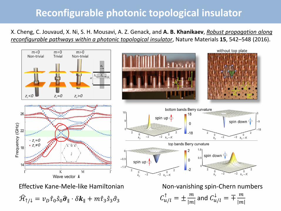
Reconfigurable photonic topological insulator
Effective Kane-Mele-like Hamiltonian Non-vanishing spin-Chern numbers
X. Cheng, C. Jouvaud, X. Ni, S. H. Mousavi, A. Z. Genack, and A. B. Khanikaev, Robust propagation along reconfigurable pathways within a photonic topological insulator, Nature Materials 15, 542–548 (2016).

Topological edge states
Reconfigurable domain wall Static non-reconfigurable interface
X. Cheng et al., Nature Materials 15, 542–548 (2016).
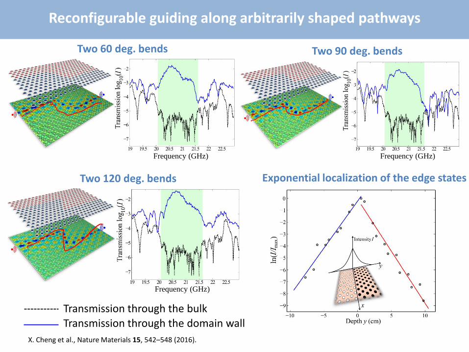
Reconfigurable guiding along arbitrarily shaped pathways
Frequency (GHz)
Two 60 deg. bends Two 90 deg. bends
Two 120 deg. bends
Frequency (GHz)
Frequency (GHz)
Exponential localization of the edge states
Transmission through the bulk
Transmission through the domain wall
X. Cheng et al., Nature Materials 15, 542–548 (2016).

3D Photonic Topological Insulatorsℋ = 𝜔0 + 𝑣|| Ƹ𝑠0 𝛿𝑘𝑥 ො𝜎𝑥 + 𝛿𝑘𝑦 ො𝜎𝑦 + 𝑣𝑧 Ƹ𝑠𝑦 ො𝜎𝑧𝛿𝑘𝑧 ±𝑚 Ƹ𝑠𝑧 ො𝜎𝑧
Ω± = ± 𝜁2 + 𝑣𝐹2 𝑘𝑥
2 + 𝑘𝑦2 + 𝑣𝑧
2𝑘𝑧2Jackiw-Rebbi-like surface states:
Slobozhanyuk, A. et al. 11, 130, Nature Photonics (2017) Yang, Y., et al., Nature (2019).

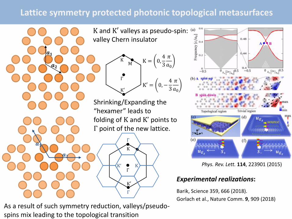
Lattice/sublattice symmetry protected photonic structures
Wu & Hu, Phys. Rev. Lett. 114, 223901 (2015).
Barik, Science 359, 666 (2018).Gorlach, Nature Comm. 9 , 909 (2018).
Examples of symmetry protected topological systems
Science 357, 61-66 (2017).
Nature 555, 342–345 (2018).
K
Γ
K′
M
K and K′ valleys as pseudo-spin: valley Chern insulator
K = 0,4
3
𝜋
𝑎0
K′ = 0,−4
3
𝜋
𝑎0
Shrinking/Expanding the “hexamer” leads to folding of K and K’ points to Γ point of the new lattice.
Γ
Γ
K
K′
Γ
KK’
As a result of such symmetry reduction, valleys/pseudo-spins mix leading to the topological transition
𝒂𝟏
𝒂𝟐
𝒂𝟏
𝒂𝟐
Lattice symmetry protected photonic topological metasurfaces
Phys. Rev. Lett. 114, 223901 (2015)
Experimental realizations:
Barik, Science 359, 666 (2018).
Gorlach et al., Nature Comm. 9, 909 (2018)
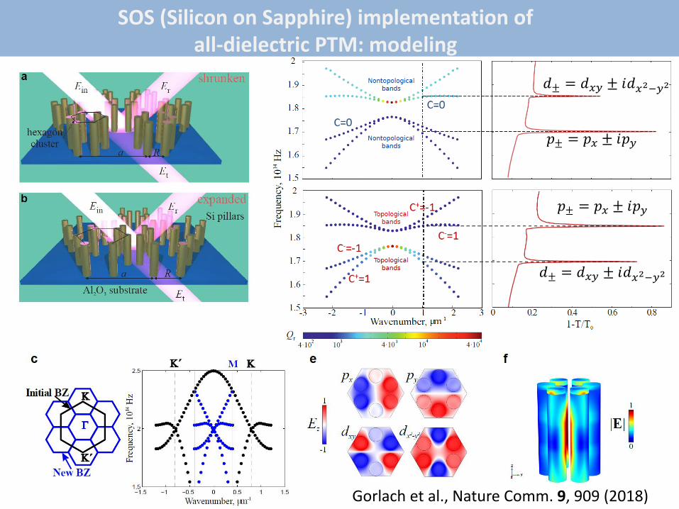
SOS (Silicon on Sapphire) implementation of all-dielectric PTM: modeling
Gorlach et al., Nature Comm. 9, 909 (2018)
𝑝± = 𝑝𝑥 ± 𝑖𝑝𝑦
𝑑± = 𝑑𝑥𝑦 ± 𝑖𝑑𝑥2−𝑦2
𝑝± = 𝑝𝑥 ± 𝑖𝑝𝑦
𝑑± = 𝑑𝑥𝑦 ± 𝑖𝑑𝑥2−𝑦2

SOS (Silicon on Sapphire) implementation and spectroscopy
(Nano-fabrication and SEM imaging was performed at the Center for Functional Nanomaterials of Brookhaven National Laboratory, spectroscopy was carried out at AK lab at City College)
Shrunk (topologically trivial)
Expanded (topologically nontrivial)
Gorlach et al., Nature Comm. 9, 909 (2018)
𝑝± = 𝑝𝑥 ± 𝑖𝑝𝑦
𝑑± = 𝑑𝑥𝑦 ± 𝑖𝑑𝑥2−𝑦2
𝑝± = 𝑝𝑥 ± 𝑖𝑝𝑦
𝑑± = 𝑑𝑥𝑦 ± 𝑖𝑑𝑥2−𝑦2

Far field imaging of the edge states
10 periods 10 periods10 periods
Trivial TrivialTopological
~30 repetitions
Gorlach et al., Nature Comm. 9, 909 (2018)
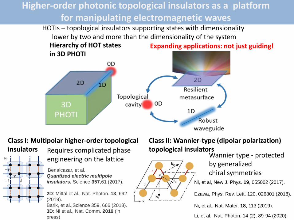
Higher-order photonic topological insulators as a platform for manipulating electromagnetic waves
HOTIs – topological insulators supporting states with dimensionality lower by two and more than the dimensionality of the system
Hierarchy of HOT states in 3D PHOTI
Expanding applications: not just guiding!
Class I: Multipolar higher-order topological insulators
Class II: Wannier-type (dipolar polarization) topological insulators
Benalcazar, et al.,
Quantized electric multipole
insulators. Science 357,61 (2017).
2D: Mittal et al., Nat. Photon. 13, 692
(2019).
Barik, et al.,Science 359, 666 (2018).
3D: Ni et al., Nat. Comm. 2019 (in
press)
Requires complicated phase engineering on the lattice
Wannier type - protected by generalized chiral symmetries
Ni, et al, New J. Phys. 19, 055002 (2017).
Ezawa, Phys. Rev. Lett. 120, 026801 (2018).
Ni, et al., Nat. Mater. 18, 113 (2019).
Li, et al., Nat. Photon. 14 (2), 89-94 (2020).

Higher-order states: simple explanation1D: Su–Schrieffer–Heeger model
𝐻 𝑘 = 𝜅 + 𝛾 cos 𝑘 ො𝜎𝑥 + 𝛾 sin 𝑘 ො𝜎𝑦
𝜈~න𝐵𝑍
⟨𝜓(𝑘)|1
𝑖
𝜕
𝜕𝑘|𝜓(𝑘)⟩ 𝑑𝑘
Bulk dipole polarization≠0
2D: Dimerized (trimerized) Kagome lattice
The “bulk polarization” 𝑝𝑖 ∶
𝑝𝑠 = 1/𝑁𝑘 σ𝑗,𝑘𝑡𝑣𝑠𝑗(𝑘𝑡) ,
where 𝜈𝑠𝑗(𝑘𝑡) is the eigenvalue (Wannier center)
of the Wilson loop, which is defined as𝑊2𝜋+𝑘𝑠←𝑘𝑠,𝑘𝑡 =
𝑢2𝜋+𝑘𝑠,𝑘𝑡 𝑢2𝜋+𝑘𝑠−𝛿𝑘,𝑘𝑡 … 𝑢𝑘𝑠+𝛿𝑘,𝑘𝑡 𝑢𝑘𝑠,𝑘𝑡
Ni, et al, New J. Phys. 19, 055002 (2017).
Ezawa, Phys. Rev. Lett. 120, 026801 (2018).
Ni, et al., Nat. Mater. 18, 113 (2019).

Excitation of bulk and corner modes at the same frequency!
Experimental design and results: embedded corner states in the bulk continuum
Zero energy states are embedded into the bulk continuum
The generalized chiral symmetry Γ3 of
the effective Hamiltonian H0:
Γ3H0Γ3−1 = H1,
Γ3H1Γ3−1 = H2,
H0 + H1 + H2 = 0.
It ensures that 𝜖1 + 𝜖2 + 𝜖3 = 0,and the presence of “zero energy”corner states.
Note: compare to regular chiral symmetry ΓH0Γ−1 = −H0, which ensures ϵ1 + ϵ2=0, or ϵ2 = −ϵ1
X. Ni, M. Weiner, A. Alu, A. B. Khanikaev, Nature Materials 12 (2018).

Two different Kagome unit cell design
Silicon pillars Holes in silicon
Photonic implementation

Two different Kagome unit cell design
Silicon pillars
Photonic implementation: New Physics
M. Li, et al. Nature Photonics 2020 (doi:s41566-019-0561-9)

Two different Kagome unit cell design
Silicon pillars Holes in silicon
Optical domain implementation

Photonic implementation: higher order 0D corner states
A. Vakulenko et al, under review.
Simulations results for the finite triangular shaped domain of topological (expanded) Kagome lattice surrounded by the shrunken (trivial) lattice.
Topological boundary modes of a higher-order topological metasurface. a, Schematic of the 2D HOTI crystal (inset) with diamond
shaped holes, and its bandstructure calculated by finite-element method (FEM) for topological (red solid lines) and gapless cases (black
dashed lines). b, c, d, show field profiles for edge, Type-I and Type-II corner modes, respectively, calculated for a finite topological lattice
surrounded by the trivial lattice. 𝑎0 is the lattice constant. Parameters used: the long size of the diamond hole is 0.71𝑎0 the short one is
0.41𝑎0. The structure is expanded or shrunken by 10%. The numbers on top of b, c, d are the eigenfrequencies of the boundary modes
(relative to the Dirac-point frequency).

DARPA NLM Quarterly Review – Polaritonic Metamaterials 31
Higher-order states induced by far-field interactionsℋ = ℋ0 + ℋNNN
ℋ0 =
0 𝐾 + 𝐽𝑒𝑖(12𝑘𝑥+
32𝑘𝑦)a0 𝐾 + 𝐽𝑒−𝑖(
12𝑘𝑥−
32𝑘𝑦)a0
𝐾 + 𝐽𝑒−𝑖(12𝑘𝑥+
32𝑘𝑦)a0 0 𝐾 + 𝐽𝑒−𝑖𝑘𝑥a0
𝐾 + 𝐽𝑒𝑖(12𝑘𝑥−
32𝑘𝑦)a0 𝐾 + 𝐽𝑒𝑖𝑘𝑥a0 0
ℋNNN = 𝐽2 ∗
0 𝑒𝑖𝑘𝑥a0 + 𝑒−𝑖(12𝑘𝑥−
32𝑘𝑦)a0 𝑒𝑖(
12𝑘𝑥+
32𝑘𝑦)a0 + 𝑒−𝑖𝑘𝑥a0
𝑒−𝑖𝑘𝑥a0 + 𝑒𝑖(12𝑘𝑥−
32𝑘𝑦)a0 0 𝑒−𝑖(
12𝑘𝑥−
32𝑘𝑦)a0 + 𝑒−𝑖(
12𝑘𝑥+
32𝑘𝑦)a0
𝑒−𝑖(12𝑘𝑥+
32𝑘𝑦)a0 + 𝑒𝑖𝑘𝑥a0 𝑒𝑖(
12𝑘𝑥−
32𝑘𝑦)a0 + 𝑒𝑖(
12𝑘𝑥+
32𝑘𝑦)a0 0
Energy spectrum of finite Kagome triangle structure with growing NNN coupling 𝐽2. Type II corner states
clearly split from edge band as 𝐽2 increases.
Next-nearest neighbor correction
M. Li, et al. Nature Photonics 2019 (doi:s41566-019-0561-9)

Air
Si - Kagomelayer
Substrate(glass n=1.45)
𝑛𝑒𝑓𝑓=1.91
Freq
uen
cy (
Hz)
Dirac cone
Light line - Air
Light line – Substrate (SiO2)
Design of HOTI SOI metasurface for optical domain
Wavenumber k (1/m)
Freq
uen
cy (
Hz)
Topological bandgap
Light line - Air
Light line – Substrate (SiO2)
364 nm
165 nm
110nm
Si 𝜖=12
Photonic metasurfacetopological band gap
a0 = 520 nm
364 nm
150 nm
78
nm
210.2 nm
Photonic metasurface with Dirac cone

Photonic implementation and probing
The Dirac cone and the topological transition takes place below the light cone; therefore the near-field solid-state immersion spectroscopy
is required for the extraction of the band structure
The shrinkage (bringing holes together) or expansion (bringing them art) leads to opening trivial and topological bandgaps, respectively, in place of the Dirac cone
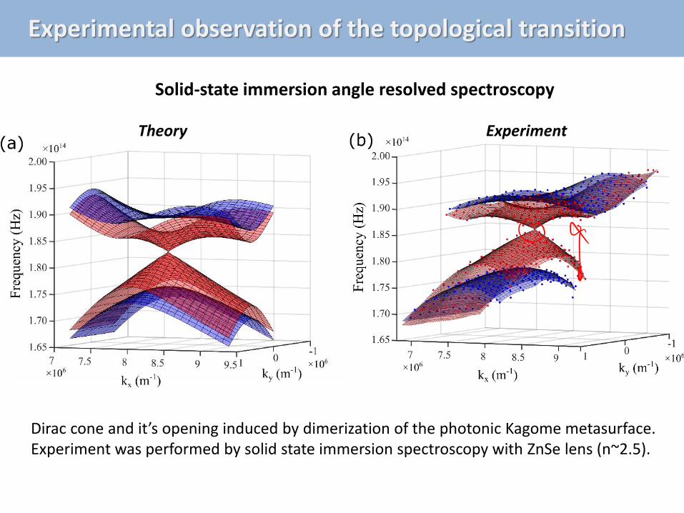
Experimental observation of the topological transition
Solid-state immersion angle resolved spectroscopy
Theory Experiment
Dirac cone and it’s opening induced by dimerization of the photonic Kagome metasurface. Experiment was performed by solid state immersion spectroscopy with ZnSe lens (n~2.5).

Experimental observation of photonic higher-order states in far-field
Experimental setup Finite triangular-shaped topological crystal surrounded by the trivial domain
Co
rne
r st
ate
sEd
ge s
tate
s

Experimental observation of photonic higher-order states in near-field
a, SEM image of a metasurface showing the topological domain surrounded by the trivial domain. Yellow dashed triangle
shows the domain wall separating topological (yellow unit cell) and trivial (purple unit cell) domains. b, near-field
amplitude distribution of the topological edge states at 6.24 µm, c, near-field images of the Type-I corner state, and, d, near-
field of the Type-II topological corner state induced by the long-range interactions at ~6.2 µm.
Near-field imaging of first- and of the two types of higher-order
topological boundary states in mid-IR.
A. Vakulenko et al, under review.
Tapping-mode atomic force microscope
(AFM) was used, where the incident p-
polarized Mid-IR light is focused onto a
commercial tip with a PtIr5 coating
(NanoWorld) that enables the light
interaction with the local near field of the
metasurface.
Excitation souce – MirCAT QCL.
The near-field profiles are plotted (in color)
over AFM topographic (grayscale) images,
and all were obtained from s-SNOM signals
demodulated at the 3rd harmonics of the
tapping frequency to subtract the
background signal.
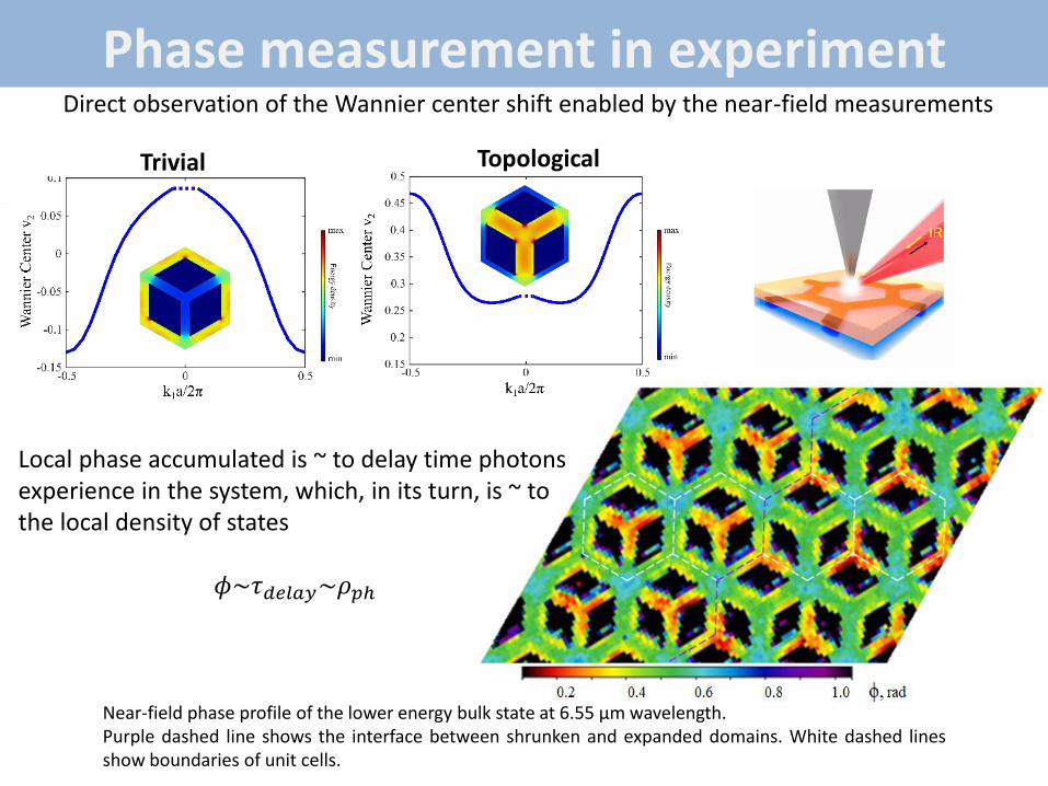
Phase measurement in experiment
Near-field phase profile of the lower energy bulk state at 6.55 µm wavelength.Purple dashed line shows the interface between shrunken and expanded domains. White dashed linesshow boundaries of unit cells.
Local phase accumulated is ~ to delay time photonsexperience in the system, which, in its turn, is ~ tothe local density of states
𝜙~𝜏𝑑𝑒𝑙𝑎𝑦~𝜌𝑝ℎ
Direct observation of the Wannier center shift enabled by the near-field measurements
Trivial Topological

Mixing light with matter – topological polaritonicsPolaritons – half-light half-matter quasi-excitaions in strongly coupled systems
✓ Quantum phenomena:BE condensation due to small mass✓ Enhanced nonlinear optical effects (solitons) ✓ Polaritonic lasers
+Topology
S. Klembt, T. H. Harder, O. A. Egorov, K. Winkler, R. Ge, M. A. Bandres, M. Emmerling, L. Worschech, T. C. H. Liew, M. Segev, C. Schneider & S. Höfling, Nature 562, 552–556 (2018).
Skolnik, Shelysh, Amo,…
Topological polaritonic states Excitonic (L/R) bands
Photonic states
Photonic states
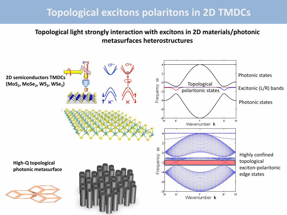
Topological light strongly interaction with excitons in 2D materials/photonic metasurfaces heterostructures
High-Q topological photonic metasurface
Highly confined topologicalexciton-polaritonic edge states
Topological excitons polaritons in 2D TMDCs
2D semiconductors TMDCs(MoS2, MoSe2, WS2, WSe2)

Topological charge/curvature transfer
Valley excitons in MoSe2
Topological Photonic bands
Photonic BS Polaritonic BS
Berry curvature/spin-Chern number is transferred to upper polariton from topological photonic band due to strong coupling
Gives rise to (photonic) pseudo-spin and valley polarized (excitonic) polaritonic topological boundary modes

Experimental observation of topological exciton-polaritons in MoSe2
Topological photonic metasurface hBN encapsulated MoSe2 on top of metasurface

Summary and Outlook
➢ Photonics offers an ideal platform for emulating topological states of condensed matter and for controlling light with synthetic gauge fields.
➢ Topological states envision a broad range of applications such as robust waveguides with controllable routing along the domain walls and integrated into classical and quantum optical systems where interaction among optical/RF elements has robust character.
42

Thank you!
Research is sponsored by the National Science Foundation and the Department of Defense
CMMI #1537294 , DMR #1626101,EFRI NewLaw #1641069, &DARPA Nascent.