Topological Insulators: Electronic structure, … Insulators: Electronic structure, material systems...
60
Network for Computational Nanotechnology UC Berkeley, Univ. of Illinois, Norfolk State, Northwestern, Purdue, UTEP Topological Insulators: Electronic structure, material systems and its applications Parijat Sengupta Network for Computational Nanotechnology Electrical and Computer Engineering Purdue University Complete set of slides from my final PhD defense Advisor : Prof. Gerhard Klimeck
Transcript of Topological Insulators: Electronic structure, … Insulators: Electronic structure, material systems...
Network for Computational Nanotechnology
(NCN)
UC Berkeley, Univ. of Illinois, Norfolk State, Northwestern, Purdue, UTEP
Topological Insulators: Electronic structure, material systems and its applications
Parijat Sengupta
Network for Computational Nanotechnology
Electrical and Computer Engineering
Purdue University
Complete set of slides from my final PhD defense Advisor : Prof. Gerhard Klimeck
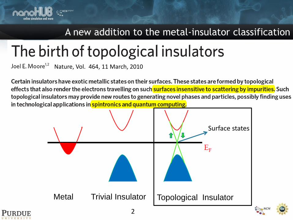
A new addition to the metal-insulator classification
2
Metal Trivial Insulator Topological Insulator
Nature, Vol. 464, 11 March, 2010
Surface states
2
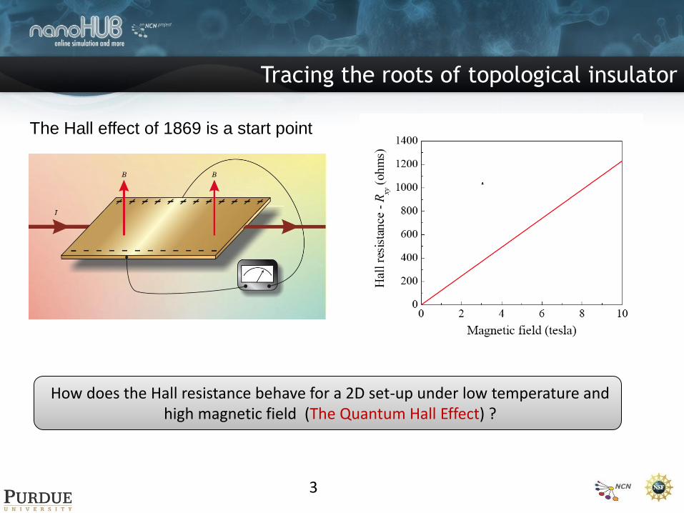
Tracing the roots of topological insulator
3
The Hall effect of 1869 is a start point
How does the Hall resistance behave for a 2D set-up under low temperature and high magnetic field (The Quantum Hall Effect) ?
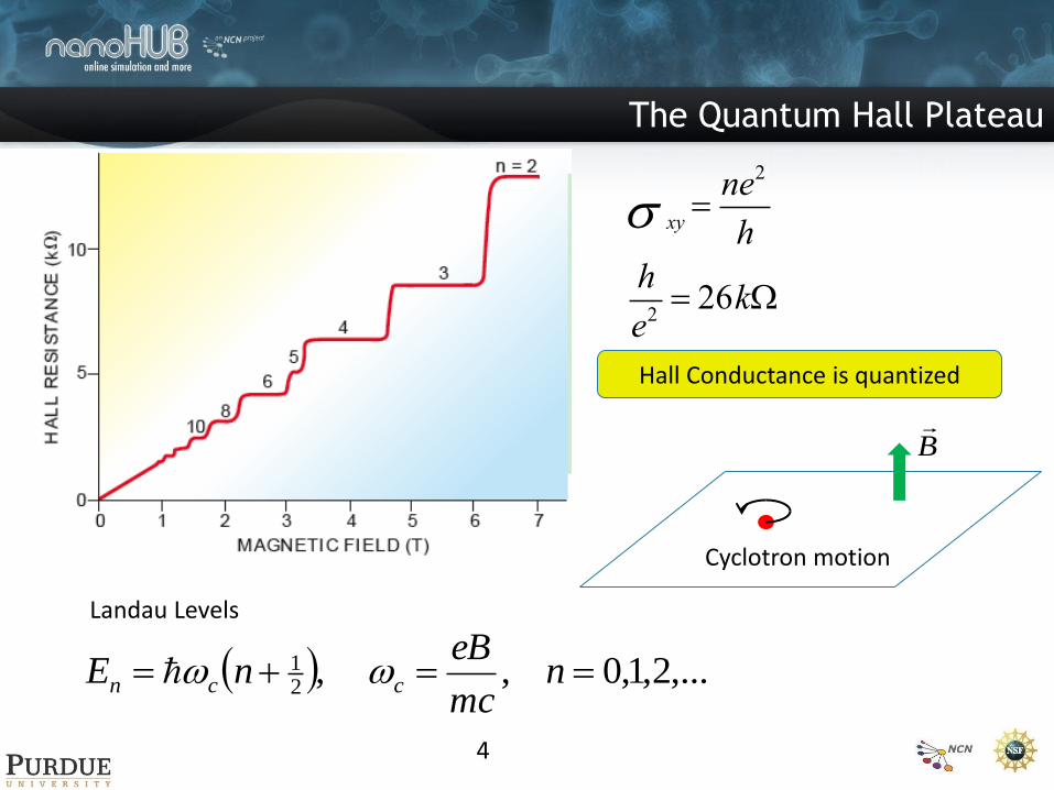
The Quantum Hall Plateau
4
Hall Conductance is quantized
xy ne2
h
h
e2 26k
,...2,1,0 , ,21 n
mc
eBnE ccn
B
Cyclotron motion
Landau Levels
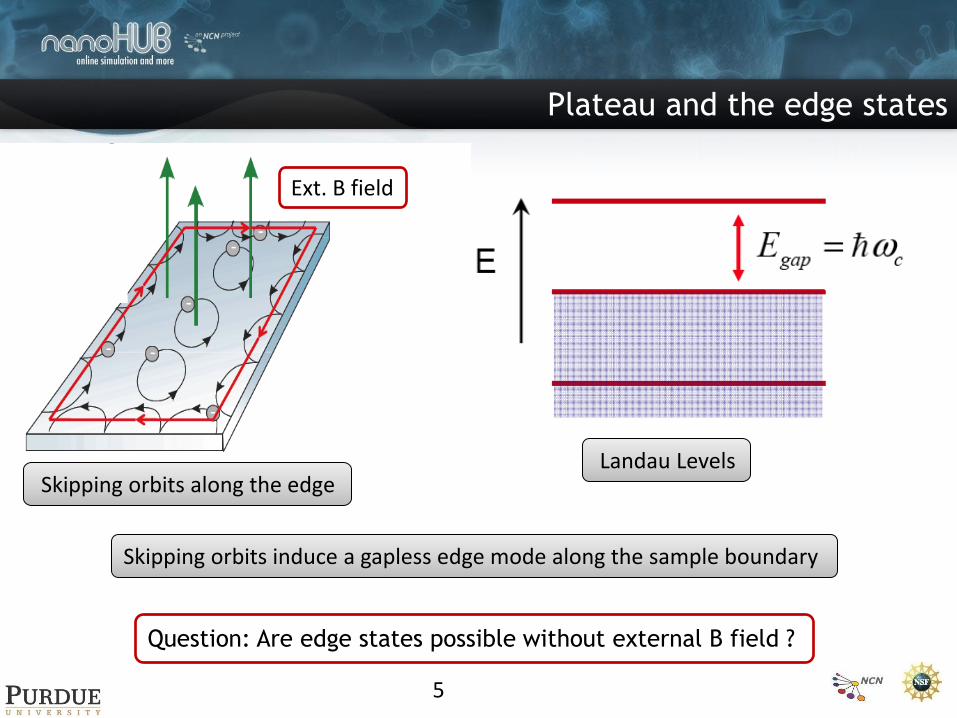
Plateau and the edge states
5
Skipping orbits induce a gapless edge mode along the sample boundary
Landau Levels Skipping orbits along the edge
Ext. B field
Question: Are edge states possible without external B field ?
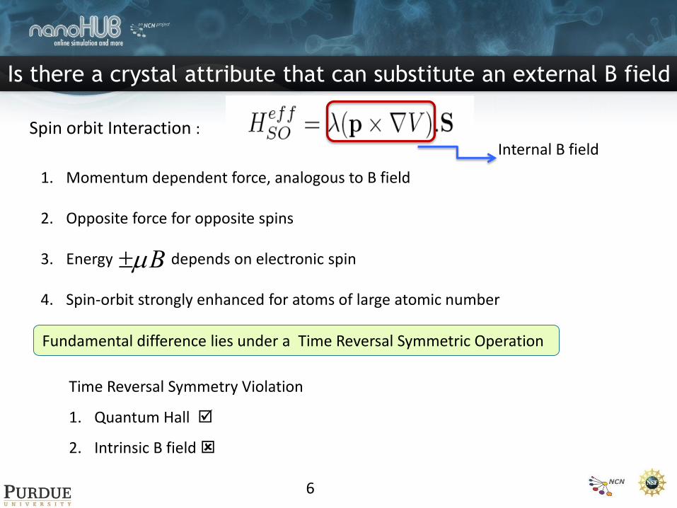
Is there a crystal attribute that can substitute an external B field
6
Spin orbit Interaction :
1. Momentum dependent force, analogous to B field
2. Opposite force for opposite spins
3. Energy depends on electronic spin
4. Spin-orbit strongly enhanced for atoms of large atomic number
B
Fundamental difference lies under a Time Reversal Symmetric Operation
Internal B field
Time Reversal Symmetry Violation
1. Quantum Hall
2. Intrinsic B field
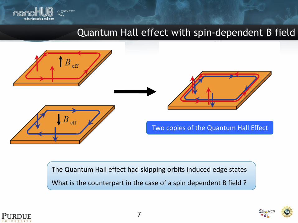
Quantum Hall effect with spin-dependent B field
7
Two copies of the Quantum Hall Effect
The Quantum Hall effect had skipping orbits induced edge states
What is the counterpart in the case of a spin dependent B field ?
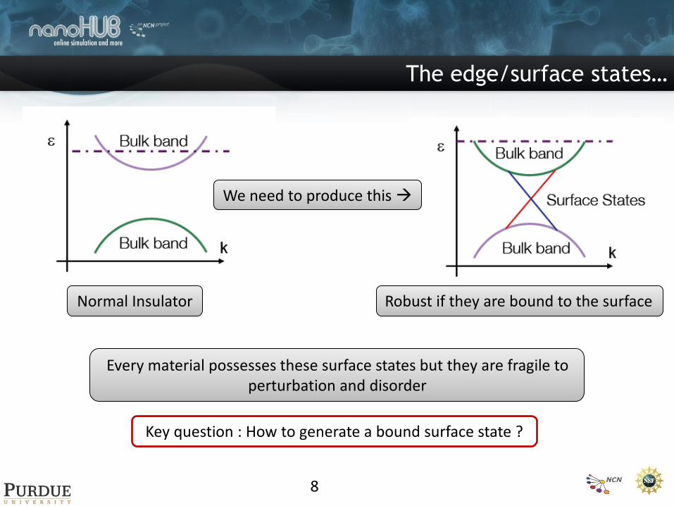
The edge/surface states…
8
Normal Insulator
We need to produce this
Every material possesses these surface states but they are fragile to perturbation and disorder
Robust if they are bound to the surface
Key question : How to generate a bound surface state ?
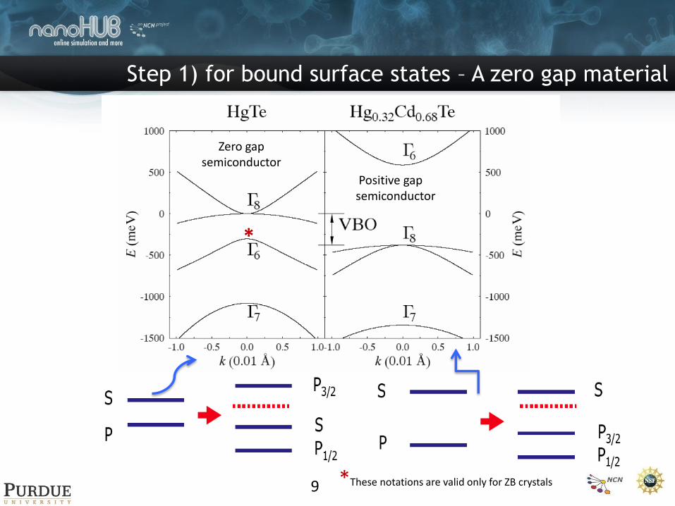
Step 1) for bound surface states – A zero gap material
9
Zero gap semiconductor
Positive gap semiconductor
*These notations are valid only for ZB crystals
*
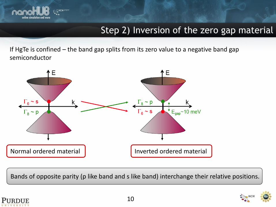
Step 2) Inversion of the zero gap material
10
If HgTe is confined – the band gap splits from its zero value to a negative band gap semiconductor
Normal ordered material Inverted ordered material
Bands of opposite parity (p like band and s like band) interchange their relative positions.
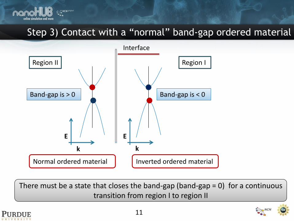
Step 3) Contact with a “normal” band-gap ordered material
11
Normal ordered material Inverted ordered material
There must be a state that closes the band-gap (band-gap = 0) for a continuous transition from region I to region II
Interface
Band-gap is > 0 Band-gap is < 0
Region I Region II
E
k
E
k
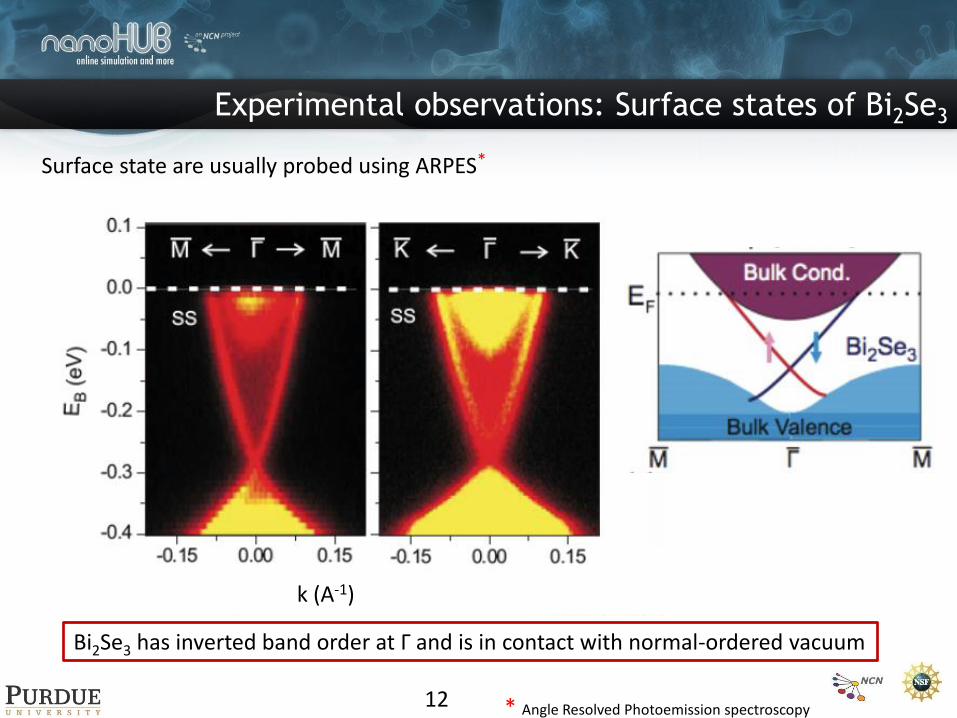
Experimental observations: Surface states of Bi2Se3
12
Surface state are usually probed using ARPES*
Bi2Se3 has inverted band order at Γ and is in contact with normal-ordered vacuum
k (A-1)
* Angle Resolved Photoemission spectroscopy
The TRIM points
13
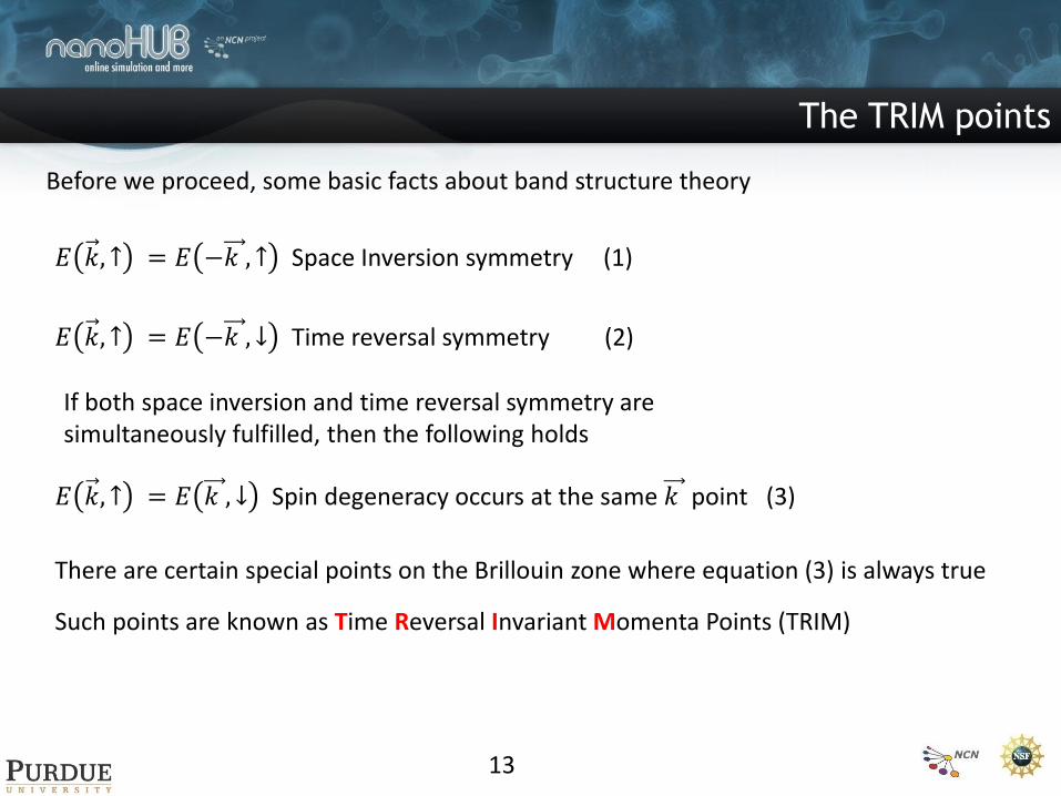
Before we proceed, some basic facts about band structure theory 𝐸 𝑘, ↑ = 𝐸 −𝑘 , ↑ Space Inversion symmetry (1)
𝐸 𝑘, ↑ = 𝐸 −𝑘 , ↓ Time reversal symmetry (2)
If both space inversion and time reversal symmetry are simultaneously fulfilled, then the following holds
𝐸 𝑘, ↑ = 𝐸 𝑘 , ↓ Spin degeneracy occurs at the same 𝑘 point (3)
There are certain special points on the Brillouin zone where equation (3) is always true
Such points are known as Time Reversal Invariant Momenta Points (TRIM)
TRIM points
14
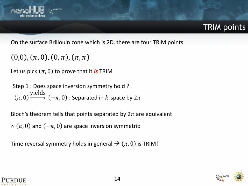
On the surface Brillouin zone which is 2D, there are four TRIM points
0,0 , 𝜋, 0 , 0, 𝜋 , 𝜋, 𝜋
Let us pick 𝜋, 0 to prove that it is TRIM Step 1 : Does space inversion symmetry hold ?
𝜋, 0yields
−𝜋, 0 : Separated in 𝑘-space by 2𝜋
Bloch’s theorem tells that points separated by 2𝜋 are equivalent
∴ 𝜋, 0 and −𝜋, 0 are space inversion symmetric
Time reversal symmetry holds in general 𝜋, 0 is TRIM!
How does the band structure appear at the TRIM points ?
15
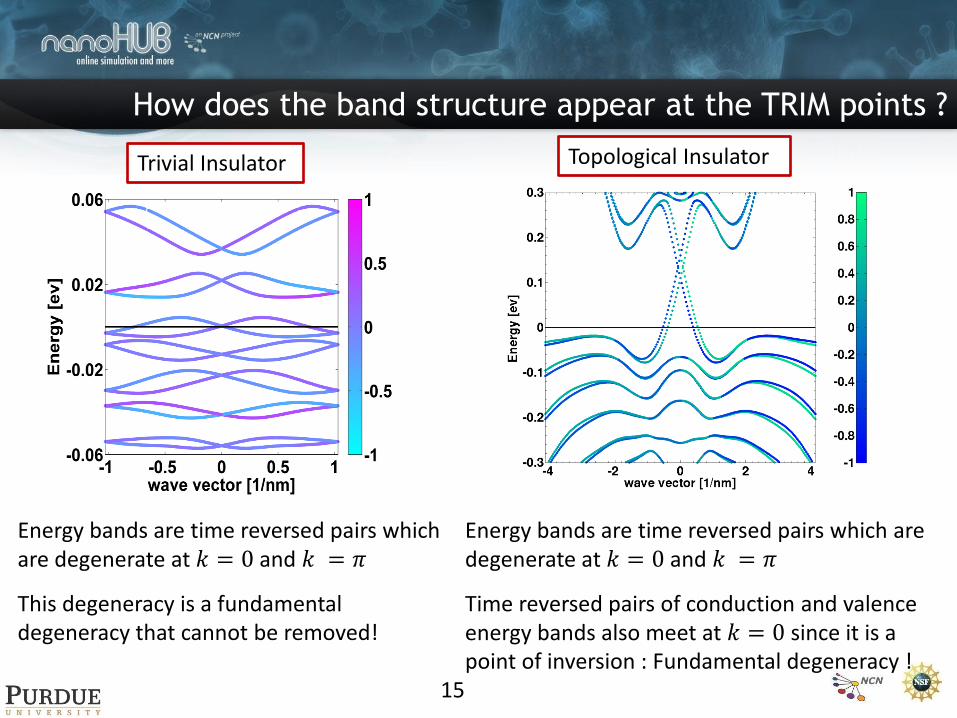
Energy bands are time reversed pairs which are degenerate at 𝑘 = 0 and 𝑘 = 𝜋
This degeneracy is a fundamental degeneracy that cannot be removed!
Trivial Insulator Topological Insulator
Energy bands are time reversed pairs which are degenerate at 𝑘 = 0 and 𝑘 = 𝜋
Time reversed pairs of conduction and valence energy bands also meet at 𝑘 = 0 since it is a point of inversion : Fundamental degeneracy !
Topology
16
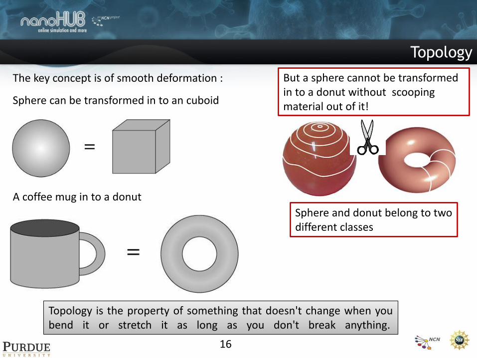
The key concept is of smooth deformation :
Sphere can be transformed in to an cuboid
A coffee mug in to a donut
But a sphere cannot be transformed in to a donut without scooping material out of it!
Topology is the property of something that doesn't change when you bend it or stretch it as long as you don't break anything.
Sphere and donut belong to two different classes
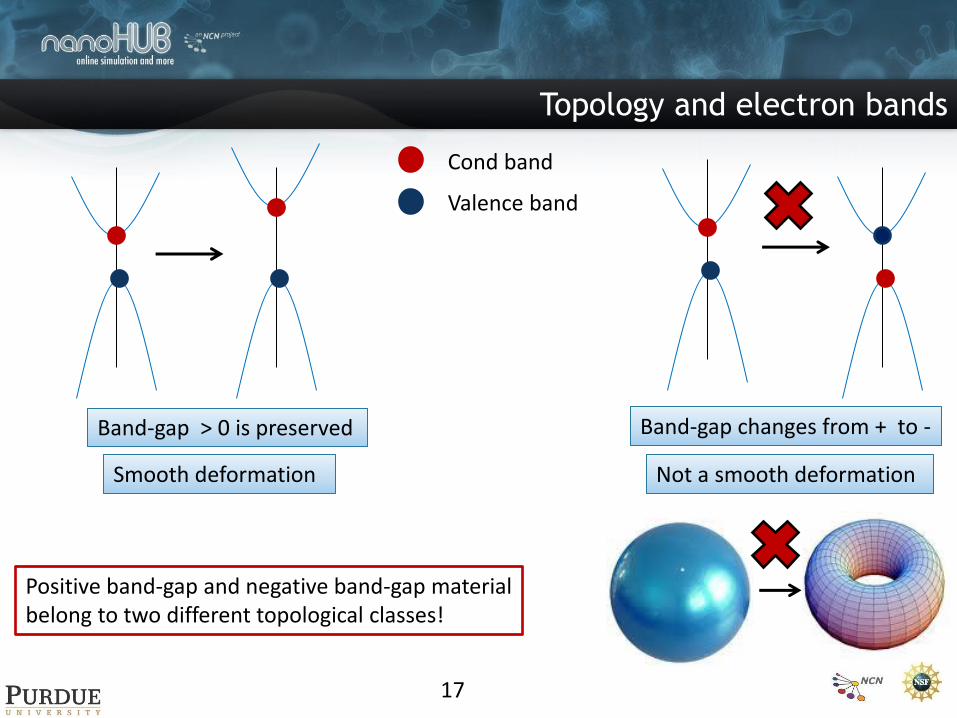
Topology and electron bands
17
Cond band
Valence band
Band-gap > 0 is preserved
Smooth deformation
Band-gap changes from + to -
Not a smooth deformation
Positive band-gap and negative band-gap material belong to two different topological classes!
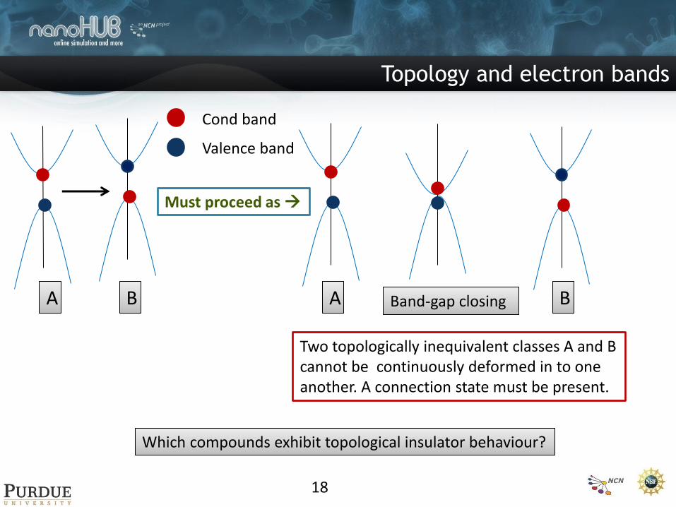
Topology and electron bands
Cond band
Valence band
A B A B Band-gap closing
Two topologically inequivalent classes A and B cannot be continuously deformed in to one another. A connection state must be present.
Must proceed as
Which compounds exhibit topological insulator behaviour?
18
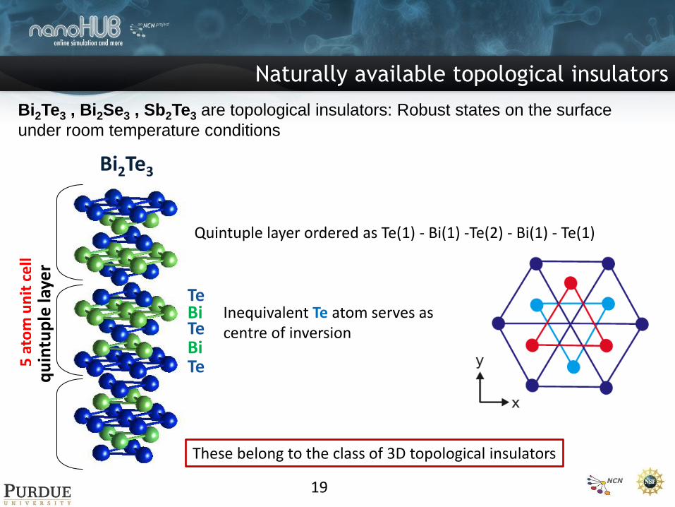
Naturally available topological insulators
19
Bi2Te3 , Bi2Se3 , Sb2Te3 are topological insulators: Robust states on the surface
under room temperature conditions
qu
intu
ple
laye
r
Te Bi Te Bi Te
Bi2Te3
Inequivalent Te atom serves as centre of inversion
Quintuple layer ordered as Te(1) - Bi(1) -Te(2) - Bi(1) - Te(1)
These belong to the class of 3D topological insulators
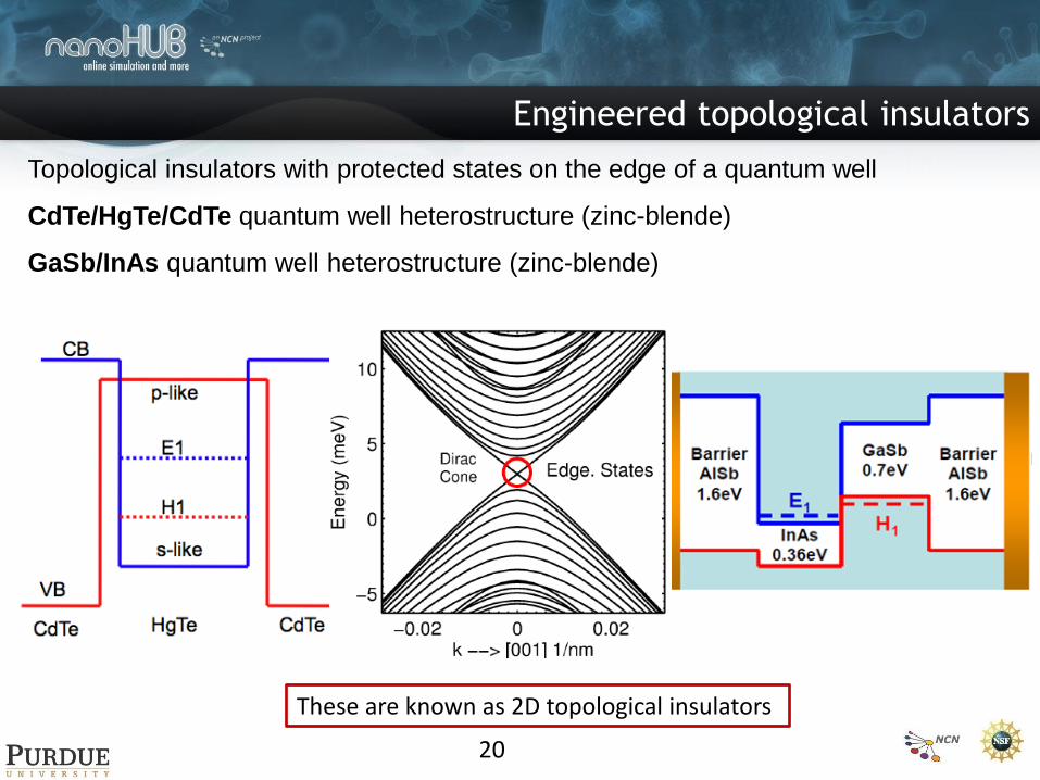
Engineered topological insulators
20
Topological insulators with protected states on the edge of a quantum well
CdTe/HgTe/CdTe quantum well heterostructure (zinc-blende)
GaSb/InAs quantum well heterostructure (zinc-blende)
These are known as 2D topological insulators
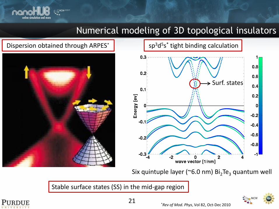
Numerical modeling of 3D topological insulators
Dispersion obtained through ARPES*
*Rev of Mod. Phys, Vol 82, Oct-Dec 2010
sp3d5s* tight binding calculation
Six quintuple layer (~6.0 nm) Bi2Te3 quantum well
Stable surface states (SS) in the mid-gap region
Surf. states
21
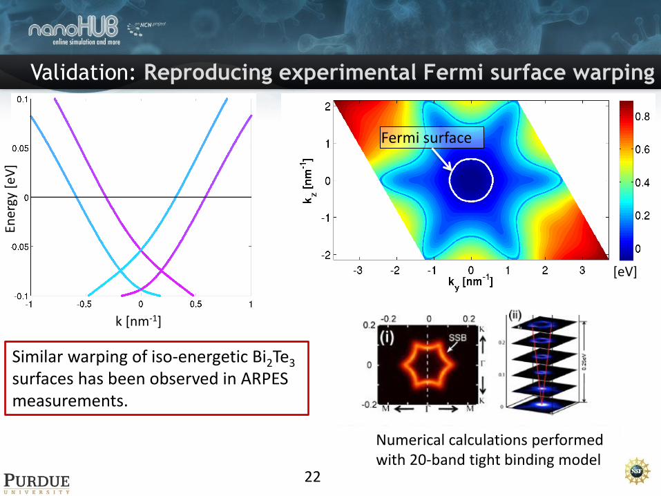
Validation: Reproducing experimental Fermi surface warping
22
Ener
gy [
eV]
k [nm-1]
[eV]
Fermi surface
Similar warping of iso-energetic Bi2Te3 surfaces has been observed in ARPES measurements.
Numerical calculations performed with 20-band tight binding model
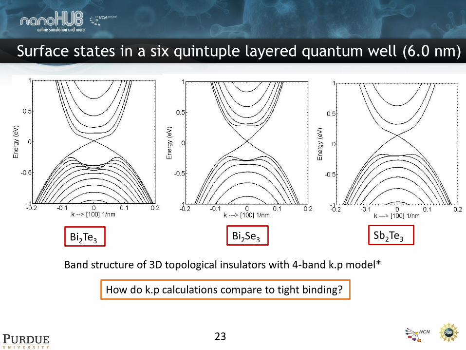
Surface states in a six quintuple layered quantum well (6.0 nm)
23
Bi2Te3 Bi2Se3 Sb2Te3
Band structure of 3D topological insulators with 4-band k.p model*
How do k.p calculations compare to tight binding?
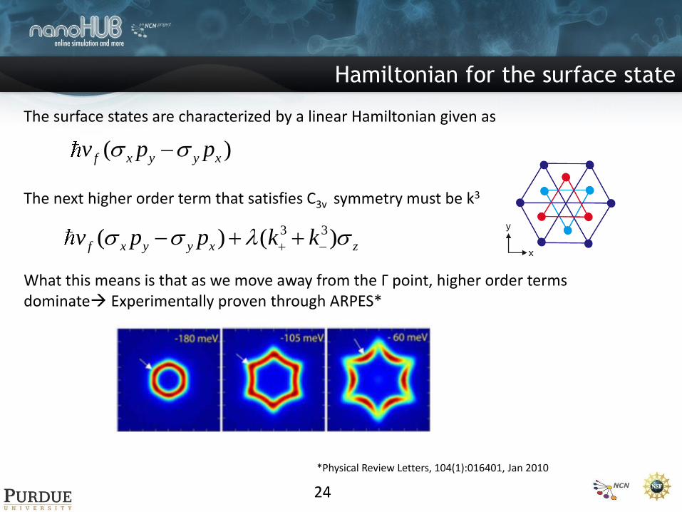
Hamiltonian for the surface state
24
The surface states are characterized by a linear Hamiltonian given as The next higher order term that satisfies C3v symmetry must be k3 What this means is that as we move away from the Γ point, higher order terms dominate Experimentally proven through ARPES*
( )f x y y xv p p
3 3( ) ( )f x y y x zv p p k k
*Physical Review Letters, 104(1):016401, Jan 2010
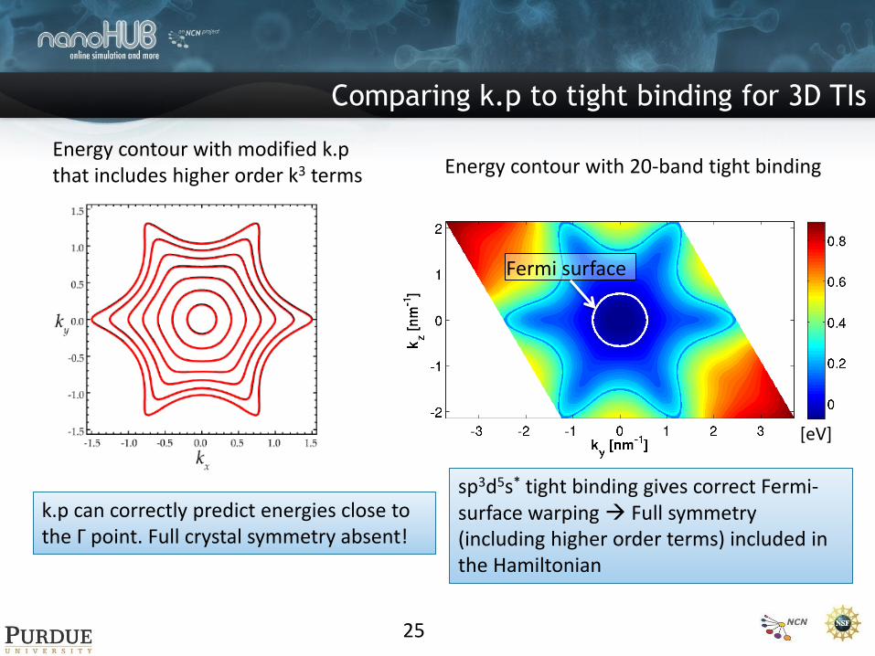
Comparing k.p to tight binding for 3D TIs
25
[eV]
Fermi surface
sp3d5s* tight binding gives correct Fermi-surface warping Full symmetry (including higher order terms) included in the Hamiltonian
k.p can correctly predict energies close to the Γ point. Full crystal symmetry absent!
Energy contour with modified k.p that includes higher order k3 terms
Energy contour with 20-band tight binding
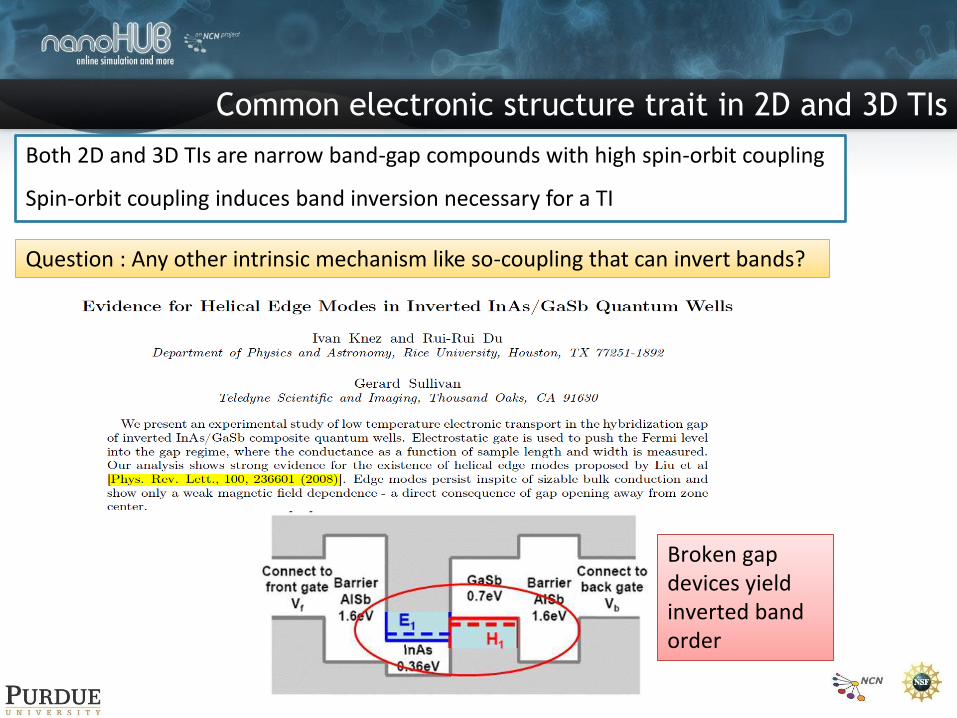
Common electronic structure trait in 2D and 3D TIs
26
Both 2D and 3D TIs are narrow band-gap compounds with high spin-orbit coupling
Spin-orbit coupling induces band inversion necessary for a TI
Question : Any other intrinsic mechanism like so-coupling that can invert bands?
Broken gap devices yield inverted band order
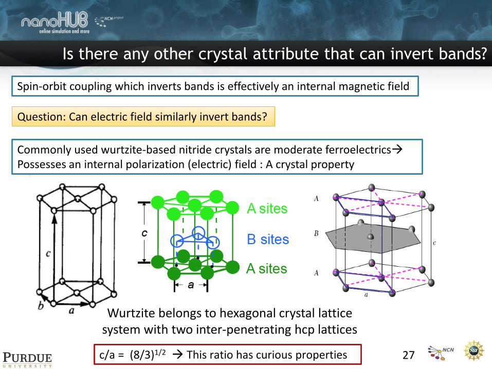
Is there any other crystal attribute that can invert bands?
27
Spin-orbit coupling which inverts bands is effectively an internal magnetic field
Question: Can electric field similarly invert bands?
Commonly used wurtzite-based nitride crystals are moderate ferroelectrics Possesses an internal polarization (electric) field : A crystal property
Wurtzite belongs to hexagonal crystal lattice system with two inter-penetrating hcp lattices
c/a = (8/3)1/2 This ratio has curious properties
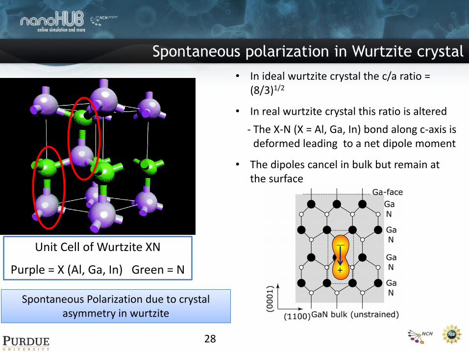
Spontaneous polarization in Wurtzite crystal
Unit Cell of Wurtzite XN
Purple = X (Al, Ga, In) Green = N
• In ideal wurtzite crystal the c/a ratio = (8/3)1/2
• In real wurtzite crystal this ratio is altered
- The X-N (X = Al, Ga, In) bond along c-axis is deformed leading to a net dipole moment
• The dipoles cancel in bulk but remain at the surface
Spontaneous Polarization due to crystal asymmetry in wurtzite
28
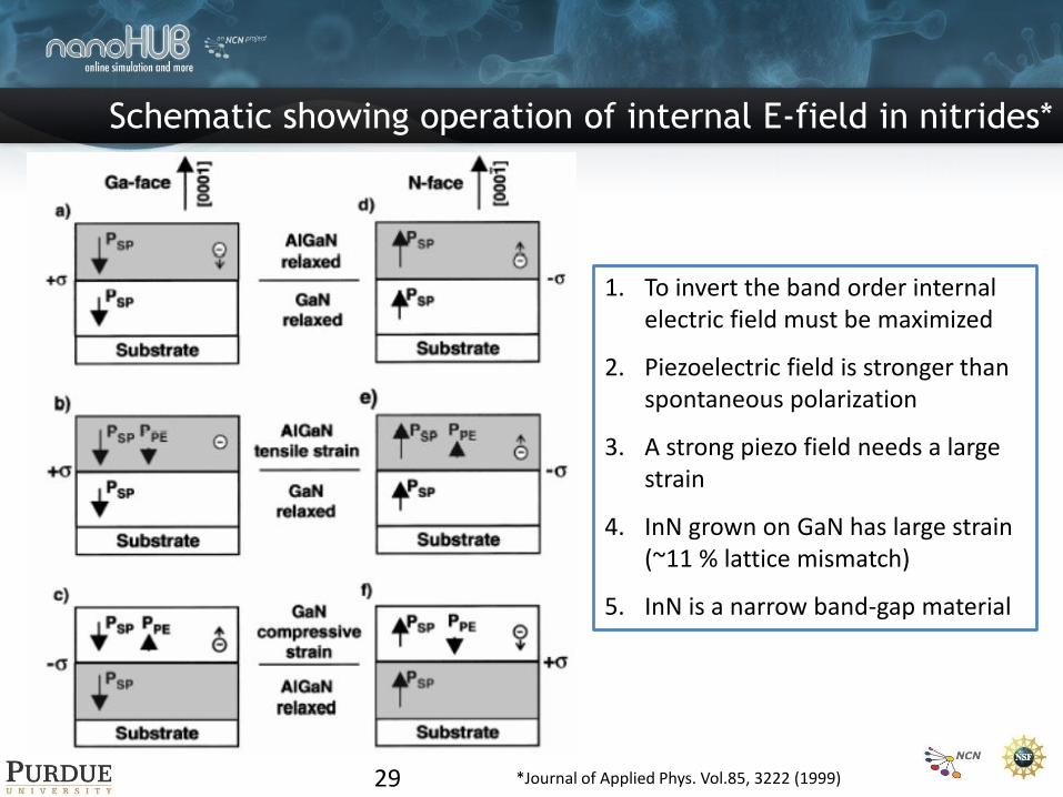
Schematic showing operation of internal E-field in nitrides*
*Journal of Applied Phys. Vol.85, 3222 (1999)
1. To invert the band order internal electric field must be maximized
2. Piezoelectric field is stronger than spontaneous polarization
3. A strong piezo field needs a large strain
4. InN grown on GaN has large strain (~11 % lattice mismatch)
5. InN is a narrow band-gap material
29
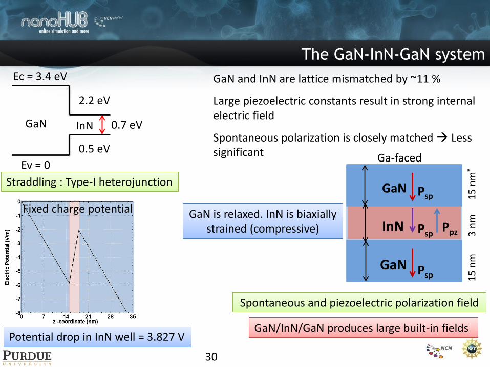
The GaN-InN-GaN system
GaN InN
0.5 eV
2.2 eV
0.7 eV
Ev = 0
Ec = 3.4 eV
Straddling : Type-I heterojunction
GaN and InN are lattice mismatched by ~11 %
Large piezoelectric constants result in strong internal electric field
Spontaneous polarization is closely matched Less significant
Ga-faced
GaN
InN
Psp
Psp Ppz
GaN Psp
GaN is relaxed. InN is biaxially strained (compressive)
Spontaneous and piezoelectric polarization field
Potential drop in InN well = 3.827 V
Fixed charge potential
GaN/InN/GaN produces large built-in fields
30
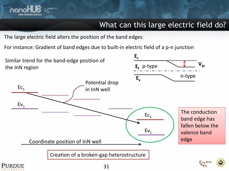
What can this large electric field do?
The large electric field alters the position of the band edges
For instance: Gradient of band edges due to built-in electric field of a p-n junction
Vbi
Ec
Ef
Ev
p-type
n-type
Similar trend for the band-edge position of the InN region
Ec1
Ev1
Ec1
Ev1
Coordinate position of InN well
The conduction band edge has fallen below the valence band edge
Creation of a broken-gap heterostructure
Potential drop in InN well
31
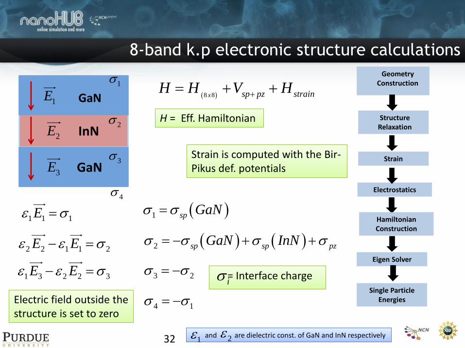
8-band k.p electronic structure calculations
Electric field outside the structure is set to zero
4
GaN
InN
GaN 1
2
3
1E
2E
3E
1 1 1E
2 2 1 1 2E E
1 3 2 2 3E E
1 sp GaN
2 sp sp pzGaN InN
3 2
4 1
Strain is computed with the Bir-Pikus def. potentials
and are dielectric const. of GaN and InN respectively 1 2
Geometry Construction
Structure Relaxation
Strain
Single Particle Energies
Eigen Solver
Electrostatics
Hamiltonian Construction
8 8x sp pz strainH H V H
H = Eff. Hamiltonian
= Interface charge i
32
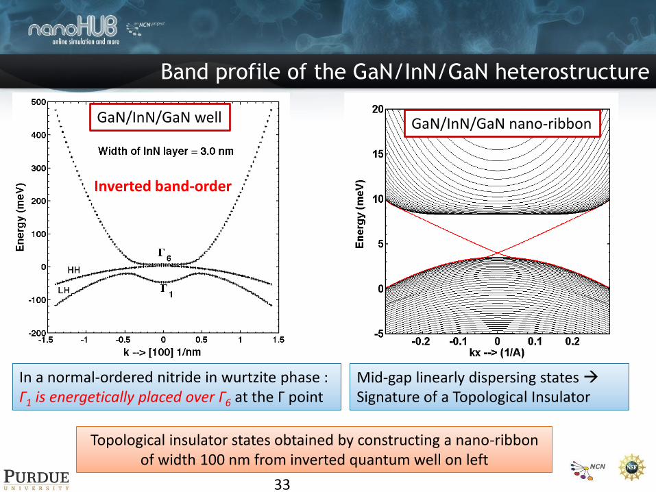
Band profile of the GaN/InN/GaN heterostructure
In a normal-ordered nitride in wurtzite phase : Γ1 is energetically placed over Γ6 at the Γ point
Inverted band-order
Mid-gap linearly dispersing states Signature of a Topological Insulator
Topological insulator states obtained by constructing a nano-ribbon of width 100 nm from inverted quantum well on left
GaN/InN/GaN well GaN/InN/GaN nano-ribbon
33
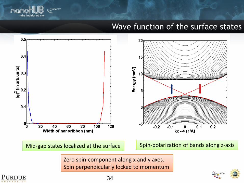
Wave function of the surface states
Mid-gap states localized at the surface Spin-polarization of bands along z-axis
Zero spin-component along x and y axes. Spin perpendicularly locked to momentum
34
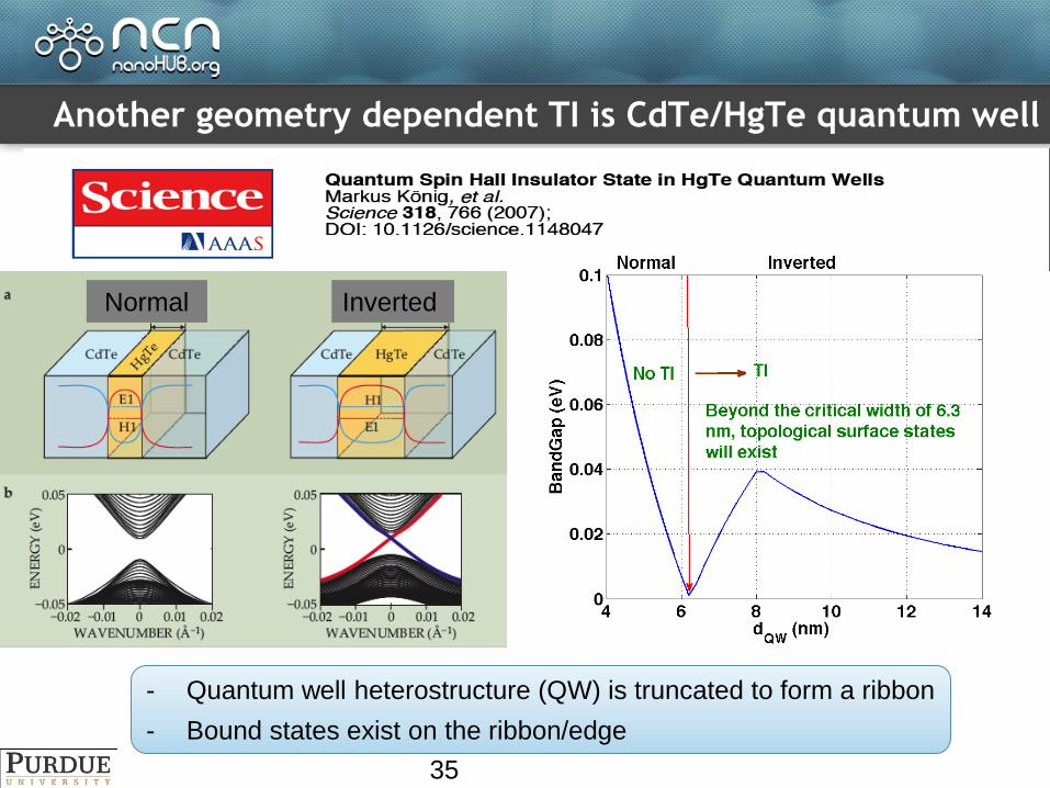
Another geometry dependent TI is CdTe/HgTe quantum well
Normal Inverted
- Quantum well heterostructure (QW) is truncated to form a ribbon
- Bound states exist on the ribbon/edge
35
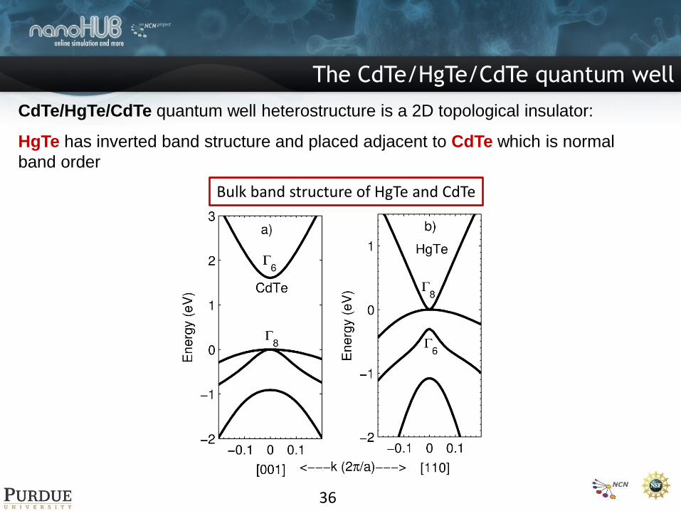
The CdTe/HgTe/CdTe quantum well
36
CdTe/HgTe/CdTe quantum well heterostructure is a 2D topological insulator:
HgTe has inverted band structure and placed adjacent to CdTe which is normal
band order
Bulk band structure of HgTe and CdTe
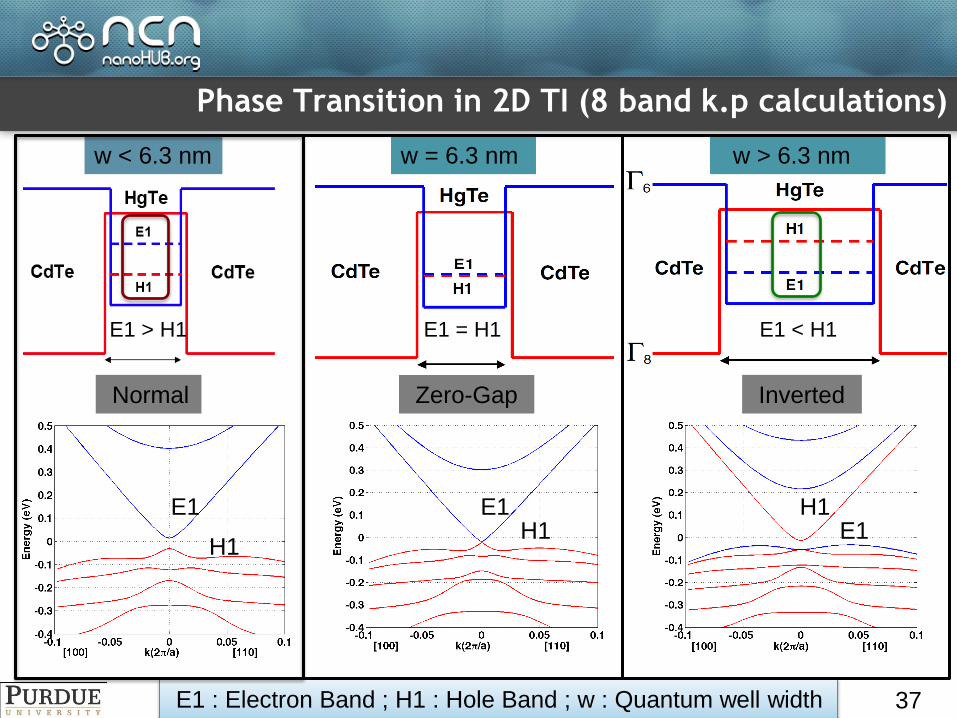
E1 < H1
E1 : Electron Band ; H1 : Hole Band ; w : Quantum well width
Phase Transition in 2D TI (8 band k.p calculations)
Zero-Gap
E1 = H1
w = 6.3 nm w > 6.3 nm
E1 < H1
w < 6.3 nm
Normal
E1
H1
E1 > H1
E1 H1
H1 E1
Inverted
37
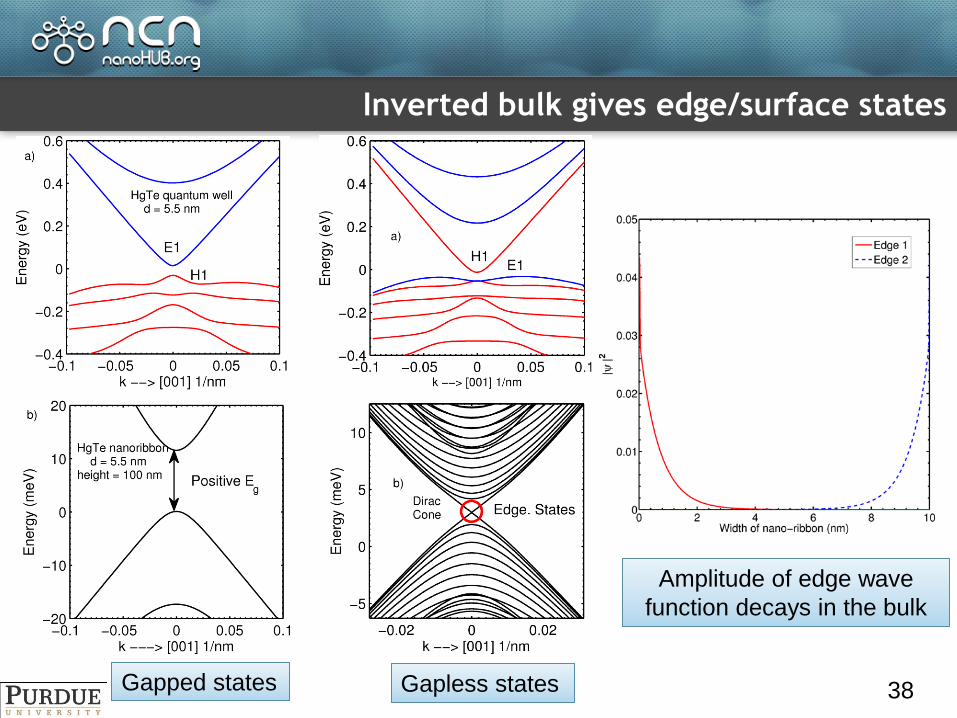
Inverted bulk gives edge/surface states
Gapped states Gapless states
Amplitude of edge wave
function decays in the bulk
38
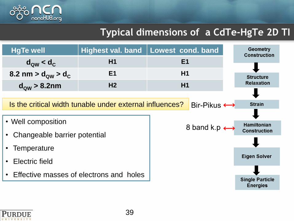
Typical dimensions of a CdTe-HgTe 2D TI
HgTe well Highest val. band Lowest cond. band
dQW < dC H1 E1
8.2 nm > dQW > dC E1 H1
dQW > 8.2nm H2 H1
• Well composition
• Changeable barrier potential
• Temperature
• Electric field
• Effective masses of electrons and holes
Is the critical width tunable under external influences?
39
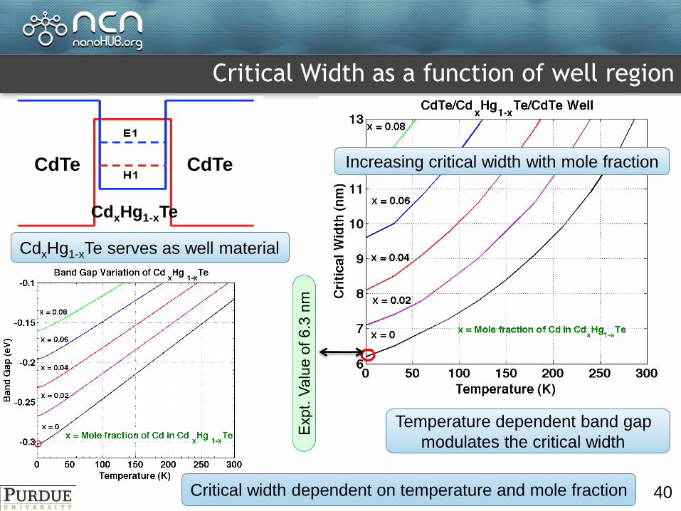
Critical Width as a function of well region
CdxHg1-xTe
CdTe CdTe
CdxHg1-xTe serves as well material
Critical width dependent on temperature and mole fraction
Temperature dependent band gap
modulates the critical width
Increasing critical width with mole fraction
40
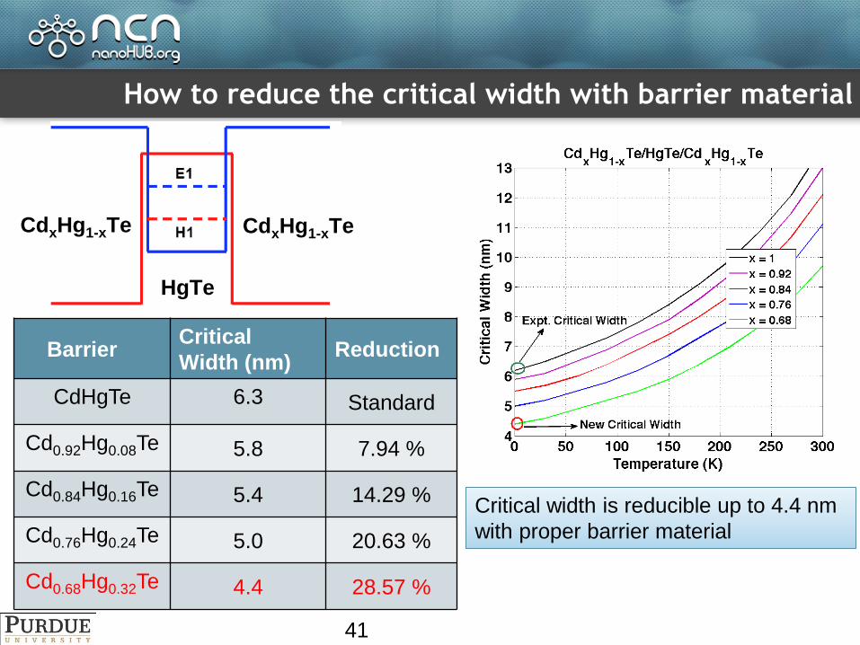
How to reduce the critical width with barrier material
HgTe
CdxHg1-xTe CdxHg1-xTe
Barrier Critical
Width (nm) Reduction
CdHgTe 6.3 Standard
Cd0.92Hg0.08Te 5.8 7.94 %
Cd0.84Hg0.16Te 5.4 14.29 %
Cd0.76Hg0.24Te 5.0 20.63 %
Cd0.68Hg0.32Te 4.4 28.57 %
Critical width is reducible up to 4.4 nm
with proper barrier material
41
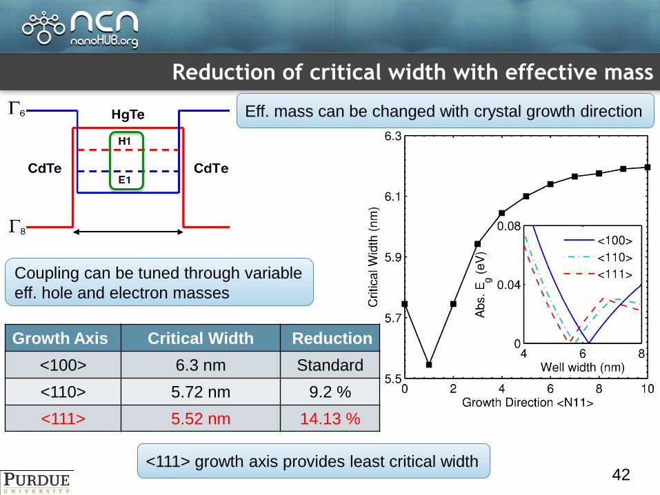
Reduction of critical width with effective mass
Coupling can be tuned through variable
eff. hole and electron masses
Eff. mass can be changed with crystal growth direction
Growth Axis Critical Width Reduction
<100> 6.3 nm Standard
<110> 5.72 nm 9.2 %
<111> 5.52 nm 14.13 %
<111> growth axis provides least critical width
42
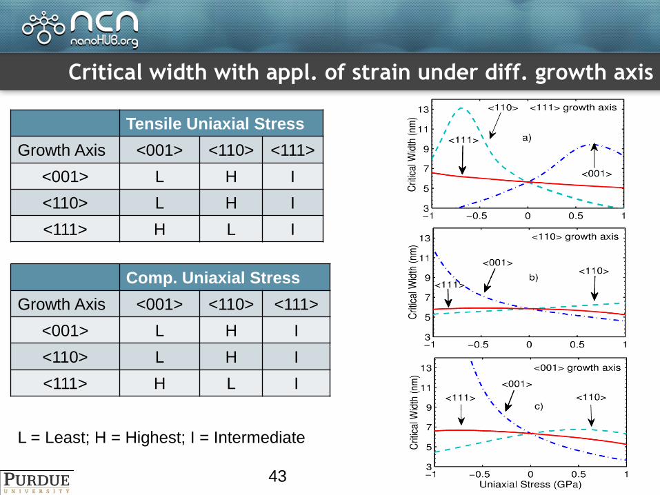
Critical width with appl. of strain under diff. growth axis
Tensile Uniaxial Stress
Growth Axis <001> <110> <111>
<001> L H I
<110> L H I
<111> H L I
Comp. Uniaxial Stress
Growth Axis <001> <110> <111>
<001> L H I
<110> L H I
<111> H L I
L = Least; H = Highest; I = Intermediate
43
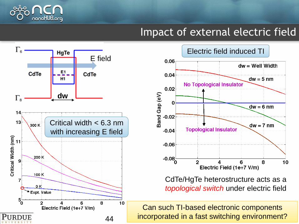
Impact of external electric field
E field Electric field induced TI
Critical width < 6.3 nm
with increasing E field
dw
CdTe/HgTe heterostructure acts as a
topological switch under electric field
Can such TI-based electronic components
incorporated in a fast switching environment? 44
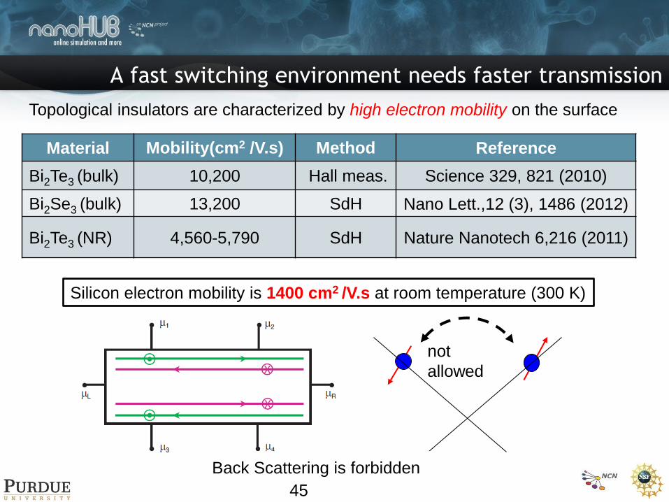
A fast switching environment needs faster transmission
Material Mobility(cm2 /V.s) Method Reference
Bi2Te3 (bulk) 10,200 Hall meas. Science 329, 821 (2010)
Bi2Se3 (bulk) 13,200 SdH Nano Lett.,12 (3), 1486 (2012)
Bi2Te3 (NR) 4,560-5,790 SdH Nature Nanotech 6,216 (2011)
Topological insulators are characterized by high electron mobility on the surface
Silicon electron mobility is 1400 cm2 /V.s at room temperature (300 K)
not
allowed
Back Scattering is forbidden
45
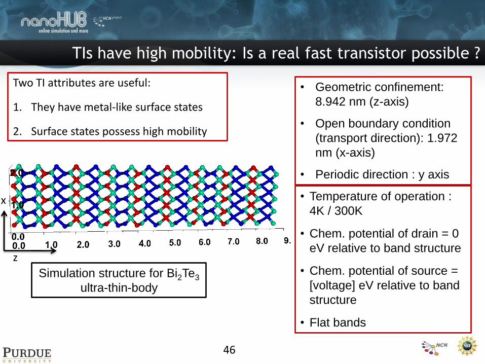
TIs have high mobility: Is a real fast transistor possible ?
46
Two TI attributes are useful:
1. They have metal-like surface states
2. Surface states possess high mobility
z
x
• Geometric confinement:
8.942 nm (z-axis)
• Open boundary condition
(transport direction): 1.972
nm (x-axis)
• Periodic direction : y axis
• Temperature of operation :
4K / 300K
• Chem. potential of drain = 0
eV relative to band structure
• Chem. potential of source =
[voltage] eV relative to band
structure
• Flat bands
Simulation structure for Bi2Te3
ultra-thin-body
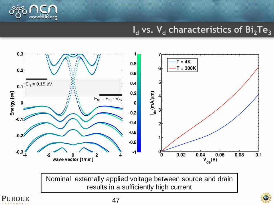
Id vs. Vd characteristics of Bi2Te3
EfS = 0.15 eV
EfD = EfS - Vds
Nominal externally applied voltage between source and drain
results in a sufficiently high current
47
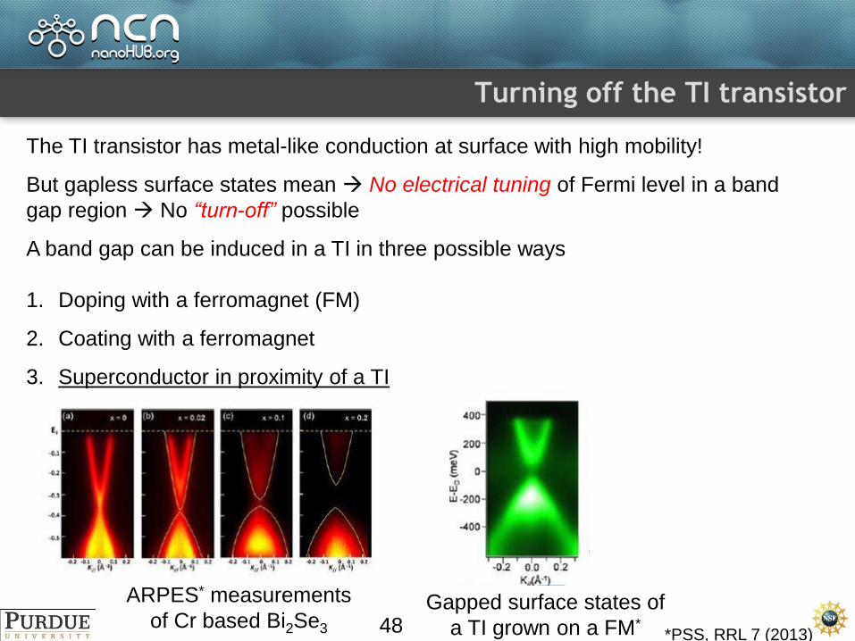
Turning off the TI transistor
The TI transistor has metal-like conduction at surface with high mobility!
But gapless surface states mean No electrical tuning of Fermi level in a band
gap region No “turn-off” possible
A band gap can be induced in a TI in three possible ways
1. Doping with a ferromagnet (FM)
2. Coating with a ferromagnet
3. Superconductor in proximity of a TI
ARPES* measurements
of Cr based Bi2Se3
Gapped surface states of
a TI grown on a FM* *PSS, RRL 7 (2013) 48
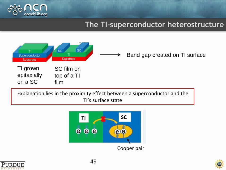
The TI-superconductor heterostructure
TI grown
epitaxially
on a SC
SC film on
top of a TI
film
Band gap created on TI surface
Explanation lies in the proximity effect between a superconductor and the TI’s surface state
Cooper pair
TI SC
49
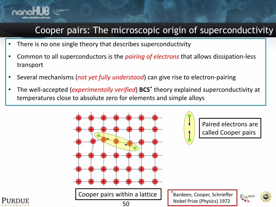
Cooper pairs: The microscopic origin of superconductivity
50
• There is no one single theory that describes superconductivity
• Common to all superconductors is the pairing of electrons that allows dissipation-less transport
• Several mechanisms (not yet fully understood) can give rise to electron-pairing
• The well-accepted (experimentally verified) BCS* theory explained superconductivity at temperatures close to absolute zero for elements and simple alloys
*Bardeen, Cooper, Schrieffer Nobel Prize (Physics) 1972
Paired electrons are called Cooper pairs
Cooper pairs within a lattice
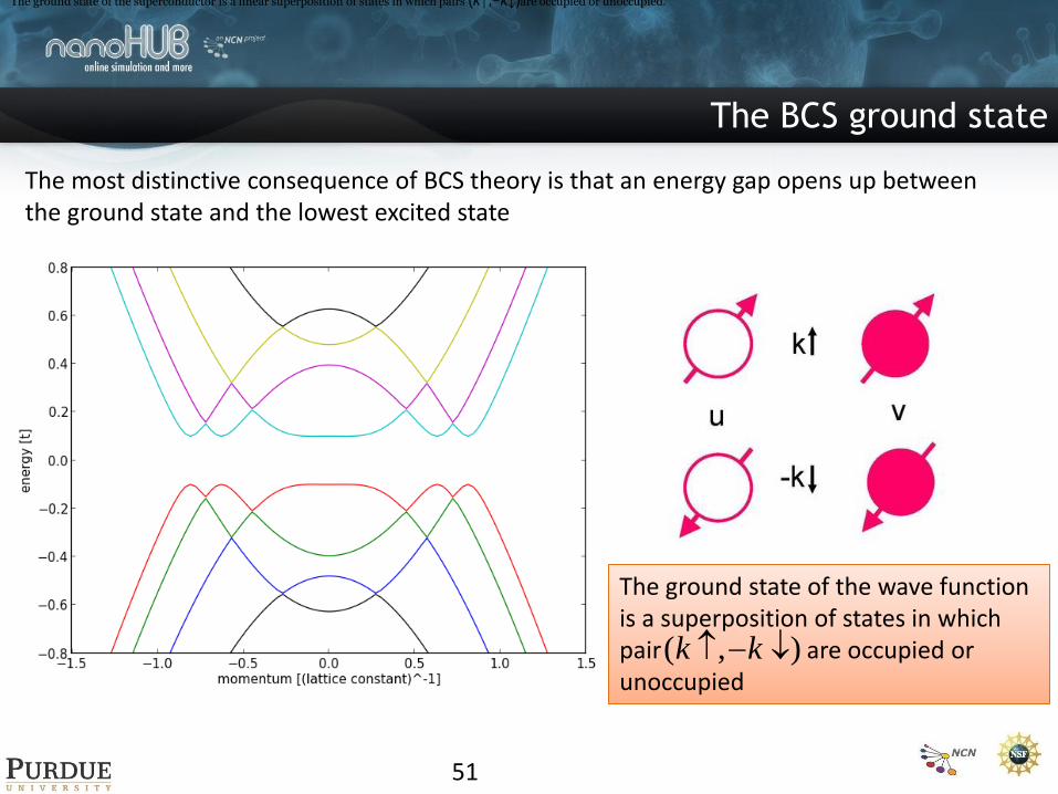
The BCS ground state
The most distinctive consequence of BCS theory is that an energy gap opens up between the ground state and the lowest excited state
The ground state of the superconductor is a linear superposition of states in which pairs (k↑,−k↓)are occupied or unoccupied.
The ground state of the wave function is a superposition of states in which pair are occupied or unoccupied
( , )k k
51
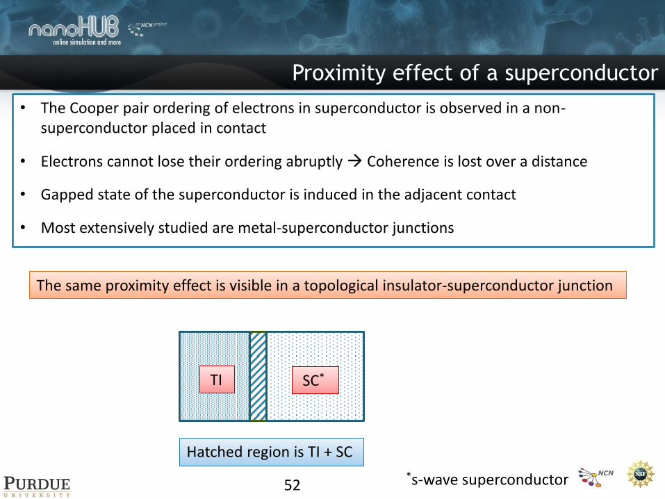
Proximity effect of a superconductor
52
• The Cooper pair ordering of electrons in superconductor is observed in a non-superconductor placed in contact
• Electrons cannot lose their ordering abruptly Coherence is lost over a distance
• Gapped state of the superconductor is induced in the adjacent contact
• Most extensively studied are metal-superconductor junctions
The same proximity effect is visible in a topological insulator-superconductor junction
TI SC SC* TI
Hatched region is TI + SC
*s-wave superconductor
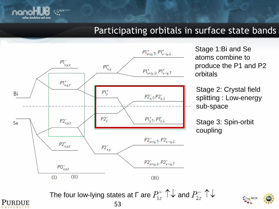
Participating orbitals in surface state bands
Stage 1:Bi and Se
atoms combine to
produce the P1 and P2
orbitals
Stage 2: Crystal field
splitting : Low-energy
sub-space
Stage 3: Spin-orbit
coupling
The four low-lying states at Γ are and
53
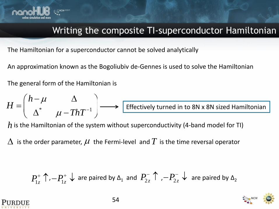
Writing the composite TI-superconductor Hamiltonian
54
The Hamiltonian for a superconductor cannot be solved analytically An approximation known as the Bogoliubiv de-Gennes is used to solve the Hamiltonian The general form of the Hamiltonian is is the Hamiltonian of the system without superconductivity (4-band model for TI) is the order parameter, the Fermi-level and is the time reversal operator
* 1
hH
ThT
h
T
Effectively turned in to 8N x 8N sized Hamiltonian
1zP , are paired by Δ1 and , are paired by Δ2 1zP 2 zP 2zP
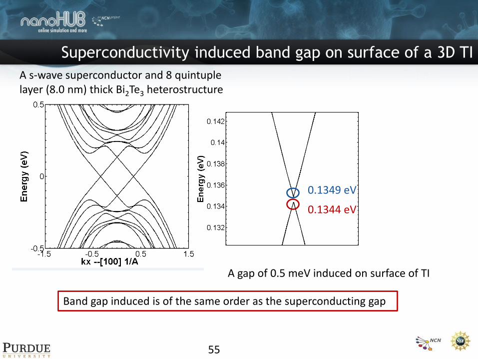
Superconductivity induced band gap on surface of a 3D TI
55
0.1349 eV
0.1344 eV
A gap of 0.5 meV induced on surface of TI
A s-wave superconductor and 8 quintuple layer (8.0 nm) thick Bi2Te3 heterostructure
Band gap induced is of the same order as the superconducting gap
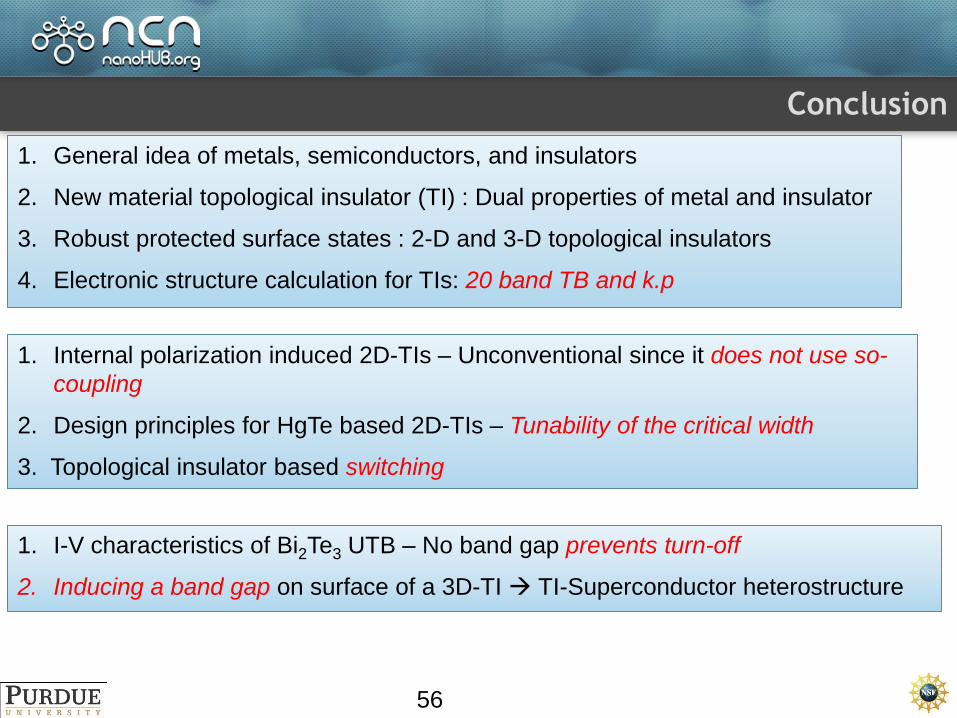
Conclusion
1. General idea of metals, semiconductors, and insulators
2. New material topological insulator (TI) : Dual properties of metal and insulator
3. Robust protected surface states : 2-D and 3-D topological insulators
4. Electronic structure calculation for TIs: 20 band TB and k.p
1. Internal polarization induced 2D-TIs – Unconventional since it does not use so-
coupling
2. Design principles for HgTe based 2D-TIs – Tunability of the critical width
3. Topological insulator based switching
1. I-V characteristics of Bi2Te3 UTB – No band gap prevents turn-off
2. Inducing a band gap on surface of a 3D-TI TI-Superconductor heterostructure
56
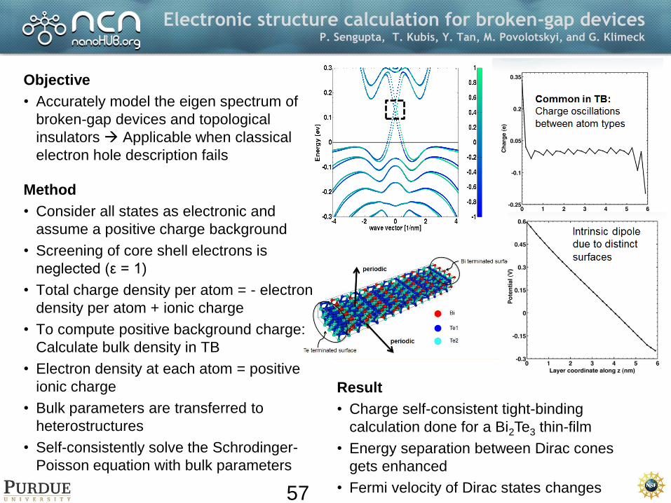
Electronic structure calculation for broken-gap devices P. Sengupta, T. Kubis, Y. Tan, M. Povolotskyi, and G. Klimeck
Objective
• Accurately model the eigen spectrum of
broken-gap devices and topological
insulators Applicable when classical
electron hole description fails
Method
• Consider all states as electronic and
assume a positive charge background
• Screening of core shell electrons is
neglected (ε = 1)
• Total charge density per atom = - electron
density per atom + ionic charge
• To compute positive background charge:
Calculate bulk density in TB
• Electron density at each atom = positive
ionic charge
• Bulk parameters are transferred to
heterostructures
• Self-consistently solve the Schrodinger-
Poisson equation with bulk parameters
Result
• Charge self-consistent tight-binding
calculation done for a Bi2Te3 thin-film
• Energy separation between Dirac cones
gets enhanced
• Fermi velocity of Dirac states changes 57
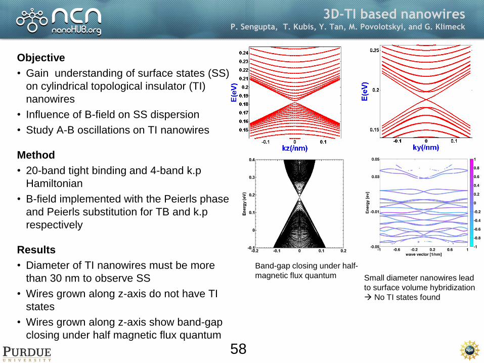
3D-TI based nanowires P. Sengupta, T. Kubis, Y. Tan, M. Povolotskyi, and G. Klimeck
Objective
• Gain understanding of surface states (SS)
on cylindrical topological insulator (TI)
nanowires
• Influence of B-field on SS dispersion
• Study A-B oscillations on TI nanowires
Method
• 20-band tight binding and 4-band k.p
Hamiltonian
• B-field implemented with the Peierls phase
and Peierls substitution for TB and k.p
respectively
Results
• Diameter of TI nanowires must be more
than 30 nm to observe SS
• Wires grown along z-axis do not have TI
states
• Wires grown along z-axis show band-gap
closing under half magnetic flux quantum
Band-gap closing under half-
magnetic flux quantum Small diameter nanowires lead
to surface volume hybridization
No TI states found
58
59
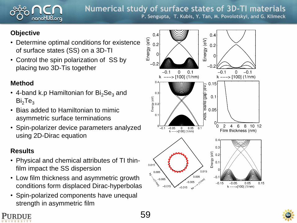
Numerical study of surface states of 3D-TI materials P. Sengupta, T. Kubis, Y. Tan, M. Povolotskyi, and G. Klimeck
Objective
• Determine optimal conditions for existence
of surface states (SS) on a 3D-TI
• Control the spin polarization of SS by
placing two 3D-Tis together
Method
• 4-band k.p Hamiltonian for Bi2Se3 and
Bi2Te3
• Bias added to Hamiltonian to mimic
asymmetric surface terminations
• Spin-polarizer device parameters analyzed
using 2D-Dirac equation
Results
• Physical and chemical attributes of TI thin-
film impact the SS dispersion
• Low film thickness and asymmetric growth
conditions form displaced Dirac-hyperbolas
• Spin-polarized components have unequal
strength in asymmetric film
59
Sponsors and Funding agencies
• Intel Corporation:
• National Science Foundation: Grant Nos.
EEC-0228390, OCI-0749140
• Semiconductor Research Corporation: Task 2141
• Computational resources at nanoHUB.org: