Today’s topic: frequency response - University of …htang/ECE5211_doc_files/ECE5211_files/...It...
46
Today’s topic: frequency response Chapter 4 1
Transcript of Today’s topic: frequency response - University of …htang/ECE5211_doc_files/ECE5211_files/...It...

Today’s topic: frequency response
Chapter 4
1

Small-signal analysis applies when transistors can be adequately characterized by their operating points and small linear changes about the points. The use of this technique has led to application of frequency-domain techniques to the analysis of the linear equivalent circuits derived from small-signal models. The transfer function of analog circuits to be discussed can be written in rational form with real-valued coefficients, that is as a ratio of polynomials in Laplace Transform variable s,

3

4.1.2 First order circuits
It is a first-order low-pass transfer function. It arises naturally when a resistance and capacitance are combined. It is often used as a simple model of more complex circuits, such as OpAmp.
4

Step response of first order circuits Another common means of characterizing linear circuits is to excite the with step inputs (such a square waveform).
5

6

4.1.3 second order low-pass H(s) with real poles
Here, w0 is the resonant or pole frequency and Q the quality factor, K the DC gain of H(s).
Equating yields
7

wp1, wp2 are widely-spaced real poles
The step response consists of two first-order terms, and when wp1 <<wp2, the second settles fast and for t >>1/wp2, the first term dominates.
8

Chapter 4 Figure 04
4.1.4 Bode plot
9

4.1.5 Second-order low-pass H(s) with complex poles
Recall
Subt. In
10

4.1.5 Second-order low-pass H(s) with complex poles 1. The step response in this case has sinusoidal term whose envelope
exponentially decays with a time constant equal to the inverse of real parts of poles, 1/wr=2Q/w0.
2. A system with high Q factor will have oscillation and ringing for some time. The oscillation frequency is determined by the imaginary parts of the poles.
3. In summary, when Q<0.5, the poles are real-valued and there is no overshoot. The borderline case Q=0.5 is called maximally-damped response. When Q>0,5, there are overshoot and ringing.
Chapter 4 Figure 09
Chapter 4 Figure 10
t
11

4.2. Frequency response of elementary circuits Small-signal analysis is implicitly assumed as only linear circuits can have well-defined frequency response. The procedure for small-signal analysis remains the same as that in Chapter 3 for single-stage amplifiers, however parasitic capacitance are now included.
12

Chapter 4 Figure 12
Chapter 4 Figure 11
4.2.1 High frequency small-signal model
13

Chapter 4 Figure 13
4.2.2 Common-source amplfier
Chapter 4 Figure 14
Note: assumed that Q1, Q2 are in active mode.
14

If
15

One more reason why analog design is tough.
16

Chapter 4 Figure 15
4.2.3 Miller effect
17

Chapter 4 Figure 17
18

Chapter 4 Figure 18
Miller effect applied to CS amplifier
Chapter 4 Figure 14
19
Miller effect allows one to quickly estimate the 3dB bandwidth in many cases.

4.2.4 Zero-value time constant method Except Miller effect, the most common and powerful technique for frequency response analysis of complex circuits is the zero-value time constant analysis method. It is very powerful in estimating a circuit’s 3dB bandwidth with minimal complication and also in determine which nodes are most important. Generally, the approach is to calculate a time-constant for each capacitor in the circuit by assuming all other capacitors are zero, then sum all time constants to estimate the 3dB bandwidth. Detailed procedure:
20

Example 4.9 (page 174)
The same as obtained previously 21
Chapter 4 Figure 14

Chapter 4 Figure 13
Design example 4.11 (page 177)
In this example, the load capacitance is modest and source resistance is high, so Cgd1 may become a major limitation of the bandwidth. This means that W1 should be small. So, given a current, Veff1 has to be relatively large: choose Veff1 to be 0.3V Then suppose L1<<L2 so that rds2>>rds1 so R2=rds1 and A0=-gm1rds1
22

Design example 4.11 (page 177) Then solve L1 to be Then note that increasing drain current of Q1 while keeping Veff1=0.3V will increase gm1 and reduce rds1 roughly in proportion, which results in about the same gain, but a smaller R2 is achieved which increase 3db bandwidth. So, bandwidth is maximized by maximizing the drain current of Q1. Then, we can compute the required gate width To ensure L2>>L1, we can take L2=3L1=0.72μm Then, we can arbitrarily and conveniently set W2=3W1
Finally, Q3 is sized to provide the desired current mirror ratio Then, need to make sure that all transistors are in active region 23

Chapter 4 Figure 13
Design example 4.12 (page 178)
In this example, the load capacitance is very large and source resistance is small, so C2 may become a major limitation of the bandwidth, so
24

Chapter 4 Figure 13
Design example 4.12 (page 178)
25
rds=2rds1

The above two design examples illustrate the manual analysis to provide an initial design solution, which thereafter needs to be refined iteratively using simulation. A number of challenges here: 1. there is no guarantee that the initial solution is valid or good; 2. the refinement may take many many iterations until a good design is achieved; 3. at each iteration, what are not working or good in the circuit, what parameters to
modify, and how to modify them requires in depth understanding of analog circuits. What about those cases when it is hard to decide which capacitance dominates? Experience counts here, after you had many designs and were aware of the biasing conditions, capacitance conditions? The time domain response of common-source amplifier? (two widely spaced poles)
26
Comments

Chapter 4 Figure 20
4.2.6 Common-gate amplifier
Chapter 3 Figure 09
27

Chapter 4 Figure 21
We estimate the time constant associated with Cgs (note that Cgs is connected between source and ground therefore may need to include Csb).
Superior 3dB bandwidth, but input impedance is too small.
28

Compared to CS amplifier, CG amplifier has much better 3dB bandwidth, but much smaller input impedance. To achieve a good tradeoff, we can combine a CG amplifier with a CS amplifier.
4.3 Cascode gain stage
Chapter 4 Figure 22
Telescopic Folded-cascode
rin2
29

Chapter 4 Figure 23
Small-signal model for the cascode
Cout=Cgd2+Cdb2+ CL+Cbias
Cs2=Cdb1+Csb2+Cgs2
Please derive Rout
Using zero-value time constant method
rin2
The total resistance seen at the drain of Q1 is
30
See Slide 21
See slides 30 (Ch3)
Miller effect

Chapter 4 Figure 24
31
On the Miller effect on Cgd1

32
Example 4.13, 4.14 (page 184-185)
Recall that a large gain of the cascode amplifier requires the Ibias to have an output resistance on the order of In this case, and especially when there is also a large load capacitance CL, the output time constant would dominate.
This approximation is valid since Rs is the same order as rds

Chapter 4 Figure 26
33
4.3 Source follower amplifier The SF amplifier may have complex poles and therefore ringing and overshoot may happen for a pulse input.
Norton equivalent circuit
Q1

Chapter 4 Figure 27
34
Cs=CL+Csb1
Chapter 4 Figure 28

35
Next we find the admittance Yg looking into the gate of Q1 (but not including Cgd1 as it is already combined into Cin’).
Recall Q<0.5 if no overshoot

36
If load capacitor Cs is very large compared to other capacitors such that
Note τCs = Cs * Rs, where Rs | || rds2
The resistance looking into the source of Q1
As RL = 0 in this case
then

Chapter 4 Figure 32
37
4.5 Differential pair When using T model for differential pair, the analysis may be simpler compared to the hybird-pi model.
CL
Vs
38
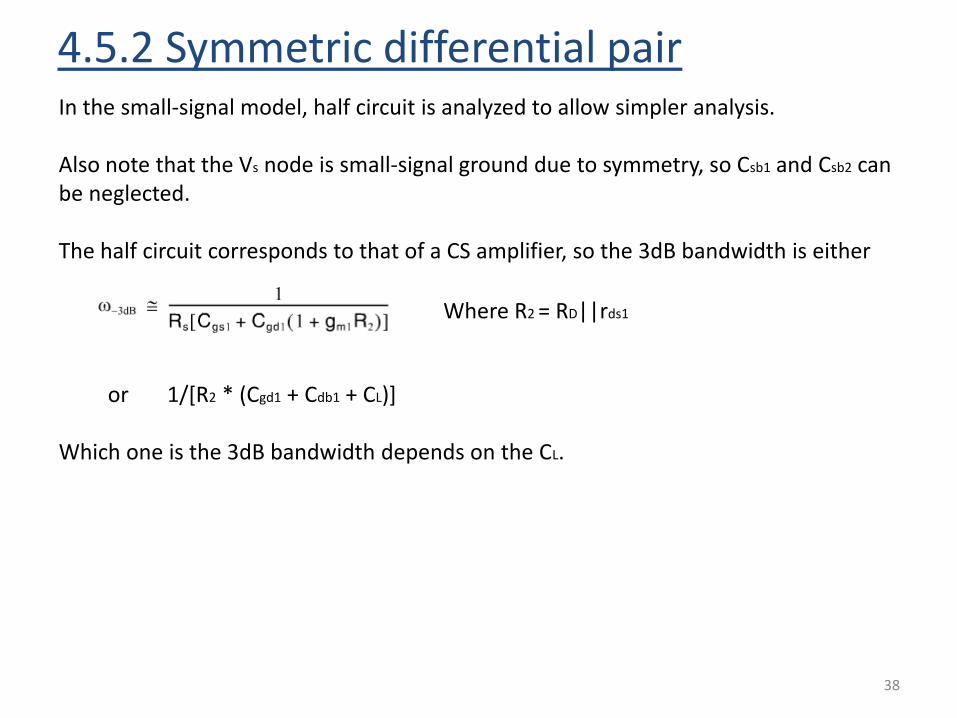
4.5.2 Symmetric differential pair In the small-signal model, half circuit is analyzed to allow simpler analysis. Also note that the Vs node is small-signal ground due to symmetry, so Csb1 and Csb2 can be neglected. The half circuit corresponds to that of a CS amplifier, so the 3dB bandwidth is either or 1/[R2 * (Cgd1 + Cdb1 + CL)] Which one is the 3dB bandwidth depends on the CL.
Where R2 = RD||rds1

39
Active loaded differential pair Again note that Vs is at small-signal ground, so half circuit can be used for analysis. Again the load capacitor will determine which one is the 3dB bandwidth.
]))//(1[( 2
1
])[//( 2
1
11311
2
313131
1
gsgdooms
b
dbdbgdgdLoo
b
CCrrgRf
CCCCCrrf
Vs

Chapter 3 Figure 19
Capacitance at input node of the current mirror: Capacitance at the output node:
Note that Q1 will conduct an current of gmVid/2 flowing through Q3 (the parallel of 1/gm3 and Cm), where we neglected the effect of rds1 and rds2, so
Va
From Miller effect
Current-mirror loaded differential pair

41
Capacitance at input node of the current mirror: Capacitance at the output node:
CL
Cm
RL
-Ix4
-Ix4
Va
Va
Io
-Ix4-Ix3

42
Capacitance at input node of the current mirror: Capacitance at the output node:
We can them multiply Gm with the total load impedance to obtain the voltage Vo
CL
Cm
RL
Io
Compared to the fully differential version, the current-mirror differential amplifier adds one more pole to the transfer function, therefore may significantly affect the frequency response.

43
Chapter 4 Figure 37
If output load capacitance is dominated, then the following simple model can be used.
Simplified small-signal model for

Chapter 4 Figure 34
44

Chapter 4 Figure 35
45

Chapter 4 Figure 36
46