TND6092 - Solving the Hearing Aid Platform Puzzle
11
© Semiconductor Components Industries, LLC, 2014 February, 2014 - Rev. 1 1 Publication Order Number: TND6092/D TND6092/D Solving the Hearing Aid Platform Puzzle Seven Things Hearing Aid Manufacturers Should Think About INTRODUCTION When it comes to developing a silicon strategy, few applications present a tougher challenge than modern hearing aids. Similar to smartphones and other mobile devices, there is a constant drive to improve performance and battery life, add new features, and retain a compact size or even reduce it. Unlike other applications, hearing aid integrated circuit designers are faced with a very low supply voltage and a power consumption requirement that is much more stringent. Often the designers must compromise between size, power consumption and performance. Figure 1. Hearing Aids SO WHAT IS DRIVING INNOVATION IN THE HEARING AID INDUSTRY? Market Trends • The sophistication and complexity of new algorithm concepts requires increased computational capabilities and more memory. • So-called “invisible” form-factors placed deep in the ear canal are driving the need for further miniaturization. • End users want seamless connectivity with smartphones and other electronic devices without the need for relay devices or other accessories. • To remain competitive, manufacturers are introducing new algorithm feature sets more frequently, shrinking product life cycles and compressing development cycles. • Manufacturers are exploring field upgradeability of algorithms enabling users to experience different feature sets in the same device during the evaluation phase, and enabling multiple upgrades after the initial purchase. • Rechargeable battery technology continues to evolve as manufacturers strive for simplicity and user convenience. • Low cost Personal Sound Amplification Products (PSAPs) are blurring the line between devices intended to compensate for hearing impairment and those intended for environmental sound amplification, possibly disrupting the market. • New business models including direct-to-consumer may possibly intensify price competition and drive component cost reduction. http://onsemi.com TECHNICAL NOTE
Transcript of TND6092 - Solving the Hearing Aid Platform Puzzle
© Semiconductor Components Industries, LLC, 2014
February, 2014 − Rev. 11 Publication Order Number:
TND6092/D
TND6092/D
Solving the Hearing AidPlatform Puzzle
Seven Things Hearing AidManufacturers Should Think About
INTRODUCTION
When it comes to developing a silicon strategy, fewapplications present a tougher challenge than modernhearing aids. Similar to smartphones and other mobiledevices, there is a constant drive to improve performanceand battery life, add new features, and retain a compact sizeor even reduce it.
Unlike other applications, hearing aid integrated circuitdesigners are faced with a very low supply voltage anda power consumption requirement that is much morestringent. Often the designers must compromise betweensize, power consumption and performance.
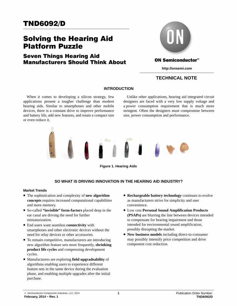
Figure 1. Hearing Aids
SO WHAT IS DRIVING INNOVATION IN THE HEARING AID INDUSTRY?
Market Trends• The sophistication and complexity of new algorithm
concepts requires increased computational capabilitiesand more memory.
• So-called “invisible” form-factors placed deep in theear canal are driving the need for furtherminiaturization.
• End users want seamless connectivity withsmartphones and other electronic devices without theneed for relay devices or other accessories.
• To remain competitive, manufacturers are introducingnew algorithm feature sets more frequently, shrinkingproduct life cycles and compressing developmentcycles.
• Manufacturers are exploring field upgradeability ofalgorithms enabling users to experience differentfeature sets in the same device during the evaluationphase, and enabling multiple upgrades after the initialpurchase.
• Rechargeable battery technology continues to evolveas manufacturers strive for simplicity and userconvenience.
• Low cost Personal Sound Amplification Products(PSAPs) are blurring the line between devices intendedto compensate for hearing impairment and thoseintended for environmental sound amplification,possibly disrupting the market.
• New business models including direct-to-consumermay possibly intensify price competition and drivecomponent cost reduction.
http://onsemi.com
TECHNICAL NOTE

TND6092/D
http://onsemi.com2
Time for a Strategic RethinkClearly the current environment is dynamic. This
significantly complicates the hardware platform decisionand also increases the strategic importance of that decision.What may have worked in the past may no longer be the rightapproach for the future.
In this technical note we identify and discuss seven keythings that hearing aid manufacturers should ponder whenthinking about the silicon strategy for their hardwareplatform:
1. Overall system challenges: Are the primarysystem challenges likely to change?
2. Digital signal processing architecture: Whicharchitecture enables a quick response to shiftingmarket needs?
3. Chip-level integration: What should be integratedon a single chip? Grouped in a package? Or keptas separate components?
4. Semiconductor process: What factors should beconsidered when moving to a smaller node?
5. Adopting standard processors in multi-corearchitectures: Is it now possible? What are thebenefits?
6. Wireless technology options: Will Made foriPhone change the game? Will a standard emerge?
7. System-level integration: Are there ways toachieve further miniaturization?
Read on for a discussion on each of these areas and thequestions they raise. We also provide our view on how tosolve the hardware platform puzzle.
While the focus is on air and bone conduction hearingaids, the discussion is also applicable to manufacturers ofcochlear implants and middle-ear devices.
1 − OVERALL SYSTEM CHALLENGES
The integrated circuits and associated silicon technologythat form the hardware platform are responsible for thecustomized amplification and manipulation of sound. Thechips may also serve user interface and wirelesscommunication functions in more advanced designs.
While some designs only require processor and memorychips, some manufacturers use as many as six, seven or evenmore chips (such as a wireless controller, wireless radio,power management, analog front end and other sensors) toachieve the functional requirements. They may also requirediscrete semiconductor components, such as capacitors andelectrostatic discharge protection devices, to be included inthe overall design. Other key system components includemicrophones, receivers, antennas and telecoils.
As a complete system, there are three primary challengesfor hearing aid designers:
1. Achieve good performance in terms of soundquality and computational capability
2. Minimize power consumption given a very lowsupply voltage (as little as ~1.0 V)
3. Minimize physical size
Figure 2. Three Primary Challenges
A decision on one impacts the others, and oftencompromise is necessary. Balancing these needs is whatmakes designing hearing aids extremely complex andchallenging. It is unlikely that this will change in theforeseeable future.

TND6092/D
http://onsemi.com3
2 − DIGITAL SIGNAL PROCESSING ARCHITECTURE
Manufacturers have a number of choices when decidingon the digital signal processing architecture for theirhardware platform. At the two extremes, these range froma closed approach to a general-purpose open-programmableapproach, with some alternative approaches in between. Themore “open” an architecture is, the greater the softwareflexibility a manufacturer has. Naturally, there are tradeoffsdepending on the chosen approach.
Closed platform architectures, also known as“fixed-function”, have the signal processing schemehardwired or hardcoded into the chip. While someparameters can be adjusted, the basic function of the chipcannot be changed without a costly and time-consumingredesign. The dedicated architecture generally results inlower energy requirements, but flexibility is sacrificed.
At the other end of the extreme is the general-purposeopen-programmable approach. With this architecturesignal-processing algorithms can be modified or updated.Since the exact software scheme is unknown, thearchitecture is designed to accommodate a wide range ofsignal processing possibilities such as sound, images and
sensor data across many applications. The compromise forthis flexibility is increased size and power consumption.Given the stringent low voltage and power consumptionrequirements, general-purpose open-programmable chipsare not suitable for hearing aids.
Million Instructions Per Second (MIPS) is a measure ofprocessor speed where a higher number implies betterperformance. Many factors influence the metric, including thetype of instructions being executed, the order of instructions,the system’s clock frequency and method of execution.A million instructions in one architecture may accomplishsignificantly more than the same number of instructions ina different architecture.
Since different architectures are used across the hearing aidindustry and a standard benchmark test does not exist,a meaningful comparison cannot be made. MIPS can,however, be useful for comparing the relative performance ofprocessors from the same manufacturer when the processorssupport the exact same instruction set.
Why MIPS is Mostly Meaningless
Figure 3. Digital Signal Processing Architecture
Between the two extremes is a semi-programmablearchitecture that attempts to overcome the disadvantage ofclosed platforms by enabling some programmability. Majorsignal processing capabilities are hardwired in logic blocks,while a programmable digital signal processor (DSP) is alsoincluded in the architecture. This enables additional signalprocessing capabilities to be implemented in softwarewithout the need to design a new chip. However, ifsignificant changes are required to the hardwired blocks, ora completely new algorithm concept cannot be addressed bythe programmable processor, then a new chip is required.While some flexibility is gained, the semi-programmableapproach still sacrifices power efficiency.
Another approach is an application-specificopen-programmable architecture. It is designed andoptimized for the signal processing needs of a very specificapplication while offering the software flexibility ofa general-purpose architecture. Though not as powerefficient as closed architectures, most of the powerefficiency disadvantage can be eliminated through efficientchip design and choice of process node, as we will explorelater in this white paper.

TND6092/D
http://onsemi.com4
Table 1. COMPARISON OF DIGITAL SIGNAL PROCESSING ARCHITECTURES
Closed (Fixed-function) Semi-programmableApplication-specificOpen-programmable
General PurposeOpen-programmable
Description Signal processinghardwired or fixed in logicblocks
Major signal processing ishardwired or fixed in logicblocksSome signal processingdefined bya programmable DSP
Degree of openness isoptimized specifically forhearing aidsAll signal processingdefined by programsrunning on aprogrammable DSP
Fully programmable andintended for a broadrange of applications
Degree of Flexibilityto Change SignalProcessing
Least flexibleSome parameters can beadjusted, but not basicfunctionality
Semi-flexibleCan solve some signalprocessing issues orchanges onprogrammable DSP
Extremely flexible withinrealm of specificapplicationNew algorithms ormodificationsimplemented in software
Most flexibleNew algorithms ormodificationsimplemented in software
Power Efficiency Most power efficient sinceexact processingrequirements are known
Moderate power efficiency Not as optimized assemi-programmable orclosed architecturesMost of the powerefficiency disadvantagecan be eliminated throughdesign and choice ofprocess node
Relatively power hungrygiven need toaccommodate a widerange of signalprocessing possibilitiesacross many applications
Summary Chip re-spin required formodifications
Some flexibility, but chipre-spin required ifhardwired signalprocessing blocks needmodification or changescannot be addressed withprogrammable DSP
Maximizes flexibility ascompletely new conceptscan be implementedwithout a chip re-spinCompromise in powerefficiency can bemitigated
Not suitable for hearingaid applications: exceedspower budget
Software Flexibility Enables InnovationThe advantages of software flexibility and the ability to
leverage hardware investment across many products andbrands greatly outweigh the advantages of a closedarchitecture. This is particularly true given the shorterproduct-life cycles, tiered performance/price points, andmicro-segmentation that is now required to offer a broad andquickly refreshed product portfolio.
The software flexibility provided by open-programmablearchitectures designed specifically for hearing aids enablesalgorithm innovation to flourish. Entirely new concepts canbe implemented on the same hardware platform,unrestrained by the hardwired limitations ofsemi-programmable or closed platforms.
This added flexibility opens up new possibilitiesincluding in-the-field upgrades of algorithm feature sets andeven the opportunity of users downloading enhancements,much like apps available for a smartphone or tablet.
These possibilities, and those yet to be imagined,underscore the value of flexibility. Manufacturers that adoptthis approach are able to respond quickly to shifting marketneeds and changes in the competitive environment withouthaving to spin new silicon. This clearly providesa competitive advantage.
3 − CHIP-LEVEL INTEGRATION
With the digital signal processing architecture approachdecided, the next decision revolves around how to partitionthe circuitry. This involves careful consideration of whichfunctional blocks and components should be combined andintegrated on a single chip, grouped and encased ina package or kept as separate components.
Main Functional Blocks
Analog Front End (AFE) – After sound has been convertedto an electrical signal by the microphones, the AFE is
responsible for conditioning and converting the signal fromanalog to digital so that it can be analyzed and manipulatedby the processor.
Processor – The “brain” of the hearing aid performs thesignal processing and controls the various tasks within theoverall hearing aid system. Given the computational-intensive needs of hearing aids, a specializedmicroprocessor called a DSP is used along with additionalcomputational units in multi-core architectures.

TND6092/D
http://onsemi.com5
Output stage – Pulse width modulation (PWM) technologyis used as a digital amplifier technique to provide normal orhigh audio output to a receiver.
Memory – Volatile memory such as Random-AccessMemory (RAM), typically integrated on the same chip as theprocessor, does not store its contents when the system ispowered down. Non-volatile memory in the form ofElectrically Erasable Programmable Read-Only Memory(EEPROM), retains its contents when powered down. It canbe programmed multiple times and is where the algorithms,fitting parameters and data logs are stored.
Power management – Optimizes and conserves the use ofpower provided by the battery.
User interface – Interface blocks enable input froma volume control, push buttons or sensors allowing the userto control the device, such as increase volume and changeprograms.
Wireless communication – Enables communicationbetween the hearing aid and external devices used to controlthe hearing aid, or send data between hearing aids or otherdevices.
In addition to these functional blocks, there are othercomponents such as capacitors and electrostatic discharge(ESD) protection circuits that are typically included ina hearing aid system.
Figure 4. Main Functional Blocks Diagram
Design Partitioning FactorsFlexibility is a key factor when making design
partitioning decisions. If blocks are integrated on a single dieas a system-on-a-chip (SoC), the ability to change a singlefunctional block is lost and the entire chip must be revised.This can potentially be both time consuming and costly. Forexample, if the wireless communication functionality iscombined with the processor into an SoC, the system islocked into a specific wireless technology.
So why not just keep all of the key functional blocks asseparate chips to maximize flexibility? Quite simply, size.There is a limited amount of available area within a hearingaid, and given the trend towards “invisible” devices, the
available area is getting smaller and smaller. This is furthercomplicated as new requirements are added, such ascommunication with multiple wireless technologies and theadoption of rechargeable battery technology. Designers arethen challenged to find ways to shrink the electronics androute the signals and power supplies between the differentchips.
A logical approach is to integrate as many blocks aspossible. While there are many advantages to integratingfunctionality as summarized in Table 2, there are also risksand business factors that need to be considered carefully.Designers also need to keep in mind the stringent size, powerconsumption and performance requirements of hearing aids.
Table 2. FACTORS TO THINK ABOUT WHEN MAKING A DESIGN PARTITIONING DECISION
System Requirements Integration Advantages Integration Risks Business Considerations
Good sound quality andcomputational performanceMinimize powerconsumptionMinimize physical size
Less power consumptionGreater efficiencyIncreased signal integritySmaller footprintSimplified manufacturing (fewer components)
Increased design complexityHigher chip manufacturingcomplexity may impact yieldLoss of flexibility in changingfunctional blocks
Increased design costsversus manufacturingcost savingsTime to market

TND6092/D
http://onsemi.com6
With the increasing complexity of hearing aids anddemand for smaller devices, a greater need exists to createa more integrated platform. In the past, hearing aidmanufacturers were reluctant to integrate the highlynoise-sensitive AFE circuitry with the digital circuitry thatis comparatively “noisy”. This was a concern whenmigrating to smaller silicon manufacturing processes.However, through clever chip design and selection of theappropriate semiconductor manufacturing process, thischallenge can be overcome. This unlocks the potential forsmaller hearing aid designs or further integration ofadditional functionality.
A Complex DecisionThere is no simple answer to design partitioning and
chip-level integration. The key is to find the optimal balancebetween all of the factors. Some blocks are relatively maturein their functionality and are prime candidates forintegration. Others, such as wireless communication, maychange depending on which technology or technologies areadopted. When this is the case, keeping the block ona separate chip is desirable, making it easier to modify theoverall system if required.
4 − SEMICONDUCTOR PROCESS
Another important factor to consider when solving thehardware platform puzzle is the semiconductor process thatwill be used to create the integrated circuits. This decisionis both influenced by the design partitioning approachdiscussed previously, as well as design challenges of certainfunctional blocks in smaller process nodes.
The desire for smaller, faster, cheaper and more reliableintegrated circuits with lower power consumption drives thedevelopment of new semiconductor tools and technologies.Primarily the market demands of mobile devices andhigh-volume consumer electronic applications havemotivated semiconductor manufacturers to seek new waysto shrink transistors the basic building blocks of anintegrated circuit.
Transition to Smaller NodesIn the case of hearing aid platforms, the increasing
sophistication of signal processing algorithms is driving theneed for greater computing capability. Transitioning toa smaller process geometry also helps address the stringentpower consumption and size constraints.
However, there are several catches.First, design and manufacturing complexity increases
significantly with smaller process nodes. There arelayout-dependant implications and strict design rules thatmust be adhered to and the number of rules increases as thenodes get smaller.
Although shrinking digital circuitry is relatively straightforward, redesigning AFE circuitry for a smaller processnode is much more challenging given the sensitivity to noise.
The second catch is cost. The full cost for design,verification, layout, mask sets, and design tools must befactored in. As shown in Figure 5, these costs significantlyrise, making the smallest nodes feasible only for extremelyhigh-volume chips. While chips designed for the 90 nmnode may have cost approximately $10 million to develop,the overall cost more than doubles for 45/40 nm designs andapproaches $40 million at the 28 nm node.
Gordon Moore, co-founder of Intel, predicted in what becameknown as “Moore’s Law” that the number of transistors that canbe placed on an integrated circuit doubles approximately everytwo years. The trend has largely held true, made possible bya continuing migration to lower process nodes, for example,from 90 nm to 65 nm to 40 nm and so on.
The smaller the numerical value of the process name, theshorter the distance between the transistors within anintegrated circuit. Shorter distances enable faster switchingand require less energy, which leads to higher performance,greater complexity and smaller die size when compared tolarger nodes.
Moore’s Law
Figure 5. Development Costs IncreaseSignificantly for Smaller Process Nodes
Sou
rce:
Inte
rnat
iona
l Bus
ines
s S
trat
egie
s, In
c.
140
130 90 65 28 2045/40 16/14
120
100
80
60
40
20
0
Process Node (nm)
Har
dwar
e D
esig
n C
ost (
$M)
IP Qualification
Architecture
Verification
Physical
Naturally, a design team that is new to a process noderequires more time to design the chip and is more likely torequire more design cycles or spins to perfect the chip,adding to development time and cost.
TND6092/D
http://onsemi.com7
Determine the Process “Sweet Spot”So what is the semiconductor process “sweet spot” for
hearing aid platforms? That can only be decided afterweighing all of the benefits and implications as summarizedin Table 3. The partitioning of key functionality must beconsidered, and as always, the overall system requirementsfor performance, power consumption and size.
Currently, some manufacturers design chips for the 65 nmprocess, but few integrate the analog front-end with theprocessor at this process node. With increasing algorithmcomplexity demanding greater computational capabilities,and the addition of new functionality putting added pressureon power consumption and miniaturization, further
migration to smaller geometries is likely. However, theeconomics will become significantly more challenging forsmaller-volume manufacturers designing their own chips.
Table 3. FACTORS TO THINK ABOUT WHEN MOVINGTO A SMALLER SEMICONDUCTOR PROCESS NODE
Pros Cons
HigherPerformance
Design complexity (more design rules,layout-dependant implications, greaterschedule unpredictability)
Lower PowerConsumption
Costs (design time, verification & layout,mask sets, design tools)
Miniaturization
5 − ADOPTING STANDARD PROCESSORS IN MULTI-CORE ARCHITECTURES
Many of today’s hearing aid platforms are based onmulti-core architectures. This is not just a trend in hearingaids, but for numerous embedded systems that arechallenged to increase performance and reduce power.
With multiple cores, different computational unitsincluding DSPs, general-purpose processors and hardwareaccelerators, often referred to as coprocessors, carry outmultiple instructions at the same time, increasing overallspeed. This becomes necessary when a single type ofprocessor is less efficient at managing a wide variety ofdiverse tasks. When combined in a single chip, higherperformance at lower power consumption can be achieved.
There are two primary drivers for the adoption ofmulti-core architectures in hearing aids:
1. Need for increased computational performanceto support more advanced algorithms based onnew audiological concepts from evidence-basedresearch; and
2. Introduction of wireless functionality for datatransfer between hearing devices, remote control,and connectivity with other electronic devices.
A widely-held misconception is that standard processingcores are not suitable for use in hearing aids. This isprimarily due to the stringent power dissipationrequirements. This has led to proprietary orcustom-designed cores being used almost exclusively.
While it is true that proprietary cores will have size andpower efficiency advantages, those advantages are
becoming smaller with deeper sub-micron technologies.Standard cores offering programmable flexibility haveevolved to where they can be used in conjunction withspecialized cores for certain processing tasks, such asrunning proprietary wireless baseband functionality tooptimize power consumption.
As summarized in Table 4, the adoption of standard coresnot only reduces overall design time-an advantage withever-shortening development schedules-but also reducesthe technical risk. With the adoption of a standard core,design resources can be redirected to other areas that deliverthe most value.
Just as other applications with stringent power constraintshave adopted standard cores as part of their multi-corearchitecture, hearing aid platforms, logically, will likelyfollow the same adoption path given the significantadvantages. The ARM® Cortex�−M3 processor is oneexample of a standard core now being used in the industry.
Table 4. ADVANTAGES OF USING A STANDARD CORE
Programmable flexibility for customization
Reduced development time
Reduced technical risk: design is verified
Available ecosystem of third-party tools and technical support
Existing technical documentation
Design reuse: portability to subsequent platforms
6 − WIRELESS TECHNOLOGY OPTIONS
Analog wireless technologies in the form of telecoil or FMsystems have been used in hearing aids for many years. Morerecently, near-field magnetic induction (NFMI) and radiofrequency (RF) technologies have been introduced. Table 5summarizes the main advantages and disadvantages of thesetwo technologies.
NFMI is limited to a range of less than 1 meter (3 feet).Therefore hearing aids using this technology must also use
an intermediary relay device to wirelessly communicateacross greater distances. Typically, Bluetooth® technologyis used for the communication link between relay device anda Bluetooth-compatible audio source. This was the designapproach first adopted by manufacturers.
Subsequently, RF technology was introduced with rangesof approximately 7 to 9 meters (23 to 30 feet). Thiseliminates the need for relay devices to be worn around the
TND6092/D
http://onsemi.com8
user’s neck or kept in close proximity. While range isextended, unless the sound source is capable of transmitting
the same frequency, an adapter must be connected to thesource to convert the signal to the appropriate frequency.
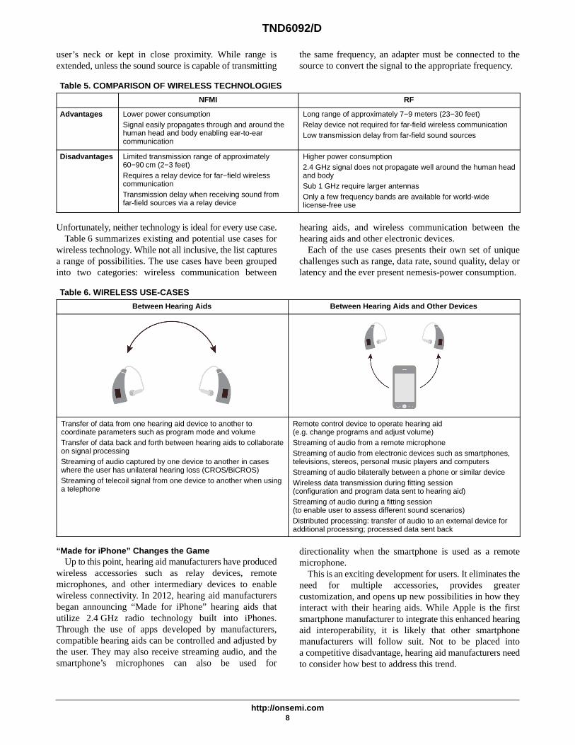
Table 5. COMPARISON OF WIRELESS TECHNOLOGIES
NFMI RF
Advantages Lower power consumptionSignal easily propagates through and around thehuman head and body enabling ear-to-ear communication
Long range of approximately 7−9 meters (23−30 feet)Relay device not required for far-field wireless communicationLow transmission delay from far-field sound sources
Disadvantages Limited transmission range of approximately60−90 cm (2−3 feet)Requires a relay device for far−field wirelesscommunicationTransmission delay when receiving sound fromfar-field sources via a relay device
Higher power consumption2.4 GHz signal does not propagate well around the human headand bodySub 1 GHz require larger antennasOnly a few frequency bands are available for world-widelicense-free use
Unfortunately, neither technology is ideal for every use case.Table 6 summarizes existing and potential use cases for
wireless technology. While not all inclusive, the list capturesa range of possibilities. The use cases have been groupedinto two categories: wireless communication between
hearing aids, and wireless communication between thehearing aids and other electronic devices.
Each of the use cases presents their own set of uniquechallenges such as range, data rate, sound quality, delay orlatency and the ever present nemesis-power consumption.
Table 6. WIRELESS USE-CASES
Between Hearing Aids Between Hearing Aids and Other Devices
Transfer of data from one hearing aid device to another tocoordinate parameters such as program mode and volumeTransfer of data back and forth between hearing aids to collaborateon signal processingStreaming of audio captured by one device to another in caseswhere the user has unilateral hearing loss (CROS/BiCROS)Streaming of telecoil signal from one device to another when usinga telephone
Remote control device to operate hearing aid (e.g. change programs and adjust volume)Streaming of audio from a remote microphoneStreaming of audio from electronic devices such as smartphones,televisions, stereos, personal music players and computersStreaming of audio bilaterally between a phone or similar deviceWireless data transmission during fitting session (configuration and program data sent to hearing aid)Streaming of audio during a fitting session (to enable user to assess different sound scenarios)Distributed processing: transfer of audio to an external device foradditional processing; processed data sent back
“Made for iPhone” Changes the GameUp to this point, hearing aid manufacturers have produced
wireless accessories such as relay devices, remotemicrophones, and other intermediary devices to enablewireless connectivity. In 2012, hearing aid manufacturersbegan announcing “Made for iPhone” hearing aids thatutilize 2.4 GHz radio technology built into iPhones.Through the use of apps developed by manufacturers,compatible hearing aids can be controlled and adjusted bythe user. They may also receive streaming audio, and thesmartphone’s microphones can also be used for
directionality when the smartphone is used as a remotemicrophone.
This is an exciting development for users. It eliminates theneed for multiple accessories, provides greatercustomization, and opens up new possibilities in how theyinteract with their hearing aids. While Apple is the firstsmartphone manufacturer to integrate this enhanced hearingaid interoperability, it is likely that other smartphonemanufacturers will follow suit. Not to be placed intoa competitive disadvantage, hearing aid manufacturers needto consider how best to address this trend.

TND6092/D
http://onsemi.com9
Will a Wireless Standard Emerge?Manufacturers have adopted a variety of digital wireless
technologies. Some have adopted NFMI at variousfrequencies while others have adopted proprietary RFtechnology in the 900 MHz and 2.4 GHz spectrums. So far,the industry has not converged on a single wireless standard.
Clearly there are benefits and trade-offs with the existingtechnologies. Whether the “Made for iPhone” trend leads toa single standard adopted by the industry remains to be seen.In the meantime, a logical question is, can multipletechnologies be used in the same set of hearing aids?
One possible approach is a dual-radio solution. This isa significant challenge given the additional silicon contentand need for multiple antennas especially when faced withthe ever-present power and size constraints. But throughclever engineering and advanced chip packagingtechniques, it is possible.
Yet another possibility is the adoption of ultra-low-powerwireless technology that may overcome existingshortcomings. If the technology reliably delivers high datarates, ear-to-ear and long-range direct audio streaming, allwith low power consumption, it may become broadlyadopted across the industry.
Why Wireless Flexibility is KeySo what does this all mean for a hardware platform today?
Things are changing quickly and the technology is stillevolving. Given the uncertainty, it makes sense to build inas much flexibility as possible for interfacing with andcontrolling different technologies, and even multiplewireless technologies. By doing so, manufacturers caneasily implement new technology as it emerges or offermultiple wireless solutions optimized for different usecases.
7 − SYSTEM-LEVEL INTEGRATION
Integrated circuits are only one piece of the puzzle inhearing aid design. Electro-acoustics and mechanical designalso play an important part.
Electro-acousticsHearing aid transducer components-microphones and
receivers-face the same miniaturization challenges asintegrated circuits. They must deliver the highest reliabilityand electro-acoustic performance as they scale down in size.Electro-acoustic system designers need to ensure theoptimal selection of transducers and their placement withinthe casing to minimize sound leakage and vibrations thatmay compromise sound quality.
Mechanical DesignMeanwhile, the mechanical design team is challenged
with taking all of the components-transducers, telecoil,battery, buttons and PCBs-and using their specializedknowledge of mechanics, electronic engineering andmaterials to figure out the optimal placement within thecasing or shell. They are constantly challenged to pushtechnological boundaries to create smaller form factors, yetmaintain manufacturability and robustness.
Integrated Circuits
Top Substrate
Interposer
Capacitors
Solder PadsMain Substrate
Solder
One recent development in advanced packaging techniques is chipstacking. By utilizing 2.5D and 3D approaches for connectingintegrated circuit die and passive components in the same package,significant space savings can be achieved.
Advances in die thinning combined with integrated passive device(IPD) technologies also help to reduce size. Vertical connectiontechniques such as through-silicon vias (TSVs) also promise evenfurther degrees of miniaturization in multi-chip stacked architectures.
Within these ultra-small packages, signal distances aredecreased and passive devices can be strategicallyplaced within the stacked architecture, improvingelectrical performance. This is particularly of interest tohearing aid manufacturers seeking additionalminiaturization and power reduction techniques.
Connections
Advanced Packaging Enables Further Miniaturization

TND6092/D
http://onsemi.com10
Putting the Pieces TogetherIt is clear that the hearing aid hardware platform cannot be
designed without considering the entire hearing aid system.Electro-acoustic and mechanical design factors must becontemplated to ensure that the overall functionality,performance, power consumption and size objectives aremet. Design teams must also be well versed in existing andemerging methods for packaging electronic components.
To create the optimal product, the hardware platformshould:• Be designed with system flexibility in mind;
• Integrate with a broad array of existing and emergingtransducers; and
• Be compatible with advanced packaging technologiesto further reduce size and power consumption.
A comprehensive systems level design approach allowsfor innovative mechanical design while ensuringcompatibility with manufacturing and assembly processes.This is critical in order to keep pace with the latestinnovations and to ensure an efficient design flow.
8 − A PIECE OF THE PUZZLE SOLVED
Developing a hardware platform strategy is a challenge.Much like solving a puzzle, it requires imagination,analytical thinking, patience and persistence.
We have identified seven things that we think hearing aidand hearing implant device manufacturers should thinkabout to solve the hardware platform puzzle.
ON Semiconductor has solved a piece of that puzzle withthe wireless-ready Ezairo 7100 DSP-based system, meetingthe stringent requirements and advanced performance needsof hearing aids and hearing implant devices. Whencombined with non-volatile memory and wireless radios, itforms a complete hardware platform.
The hearing aid market is dynamic and the technology isever evolving. Given the emerging trends and level ofuncertainty, flexibility is a must.
As an integrated system, Ezairo 7100 provides built-inflexibility to support evolving algorithm, wireless andsystem-level needs. It includes an analog front-end,multi-core processing, wireless control and powermanagement functionality, all on a single chip.
The new series builds on the company’s successfulopen-programmable DSP-based systems, including theEzairo 5900 and Ezairo 6200 series. Ezairo 7100 systems areavailable as die or as packaged integrated circuits.
Table 7. SOLVING THE HARDWARE PLATFORM PUZZLE
Seven Things to Think About Ezairo 7100 Solves a Piece of the Puzzle
1 Overall SystemChallenges
Delivers on performance, size and power consumption: the industry’s most integrated, mostpower efficient (< 500��W) chip with 5X the performance of the previous generation
2 Digital SignalProcessing Architecture
Open architecture specifically designed for hearing aid and hearing implant devices to maximizeprogrammable flexibility for evolving algorithm features
3 Chip-level Integration AFE, processing, wireless control and power management integrated on a single chip
4 Semiconductor Process Manufactured in 65 nm process to produce the industry’s smallest and most power efficientintegrated chip
5 Adopting StandardProcessors in Multi-core
Architectures
Utilizing ARM® Cortex�−M3 processor−an industry first
6 Wireless TechnologyOptions
Built-in wireless flexibility to control different kinds and even multiple wireless radios
7 System-level Integration Built-in flexibility to interface with a wide range of transducers and other components that may beincluded in the overall system, or may be adopted in the future

TND6092/D
http://onsemi.com11
Figure 6. Ezairo 7100 Arch Diagram
ON Semiconductor and are registered trademarks of Semiconductor Components Industries, LLC (SCILLC). SCILLC owns the rights to a number of patents, trademarks,copyrights, trade secrets, and other intellectual property. A listing of SCILLC’s product/patent coverage may be accessed at www.onsemi.com/site/pdf/Patent−Marking.pdf. SCILLCreserves the right to make changes without further notice to any products herein. SCILLC makes no warranty, representation or guarantee regarding the suitability of its products for anyparticular purpose, nor does SCILLC assume any liability arising out of the application or use of any product or circuit, and specifically disclaims any and all liability, including withoutlimitation special, consequential or incidental damages. “Typical” parameters which may be provided in SCILLC data sheets and/or specifications can and do vary in different applicationsand actual performance may vary over time. All operating parameters, including “Typicals” must be validated for each customer application by customer’s technical experts. SCILLCdoes not convey any license under its patent rights nor the rights of others. SCILLC products are not designed, intended, or authorized for use as components in systems intended forsurgical implant into the body, or other applications intended to support or sustain life, or for any other application in which the failure of the SCILLC product could create a situation wherepersonal injury or death may occur. Should Buyer purchase or use SCILLC products for any such unintended or unauthorized application, Buyer shall indemnify and hold SCILLC andits officers, employees, subsidiaries, affiliates, and distributors harmless against all claims, costs, damages, and expenses, and reasonable attorney fees arising out of, directly or indirectly,any claim of personal injury or death associated with such unintended or unauthorized use, even if such claim alleges that SCILLC was negligent regarding the design or manufactureof the part. SCILLC is an Equal Opportunity/Affirmative Action Employer. This literature is subject to all applicable copyright laws and is not for resale in any manner.
PUBLICATION ORDERING INFORMATIONN. American Technical Support: 800−282−9855 Toll FreeUSA/Canada
Europe, Middle East and Africa Technical Support:Phone: 421 33 790 2910
Japan Customer Focus CenterPhone: 81−3−5817−1050
TND6092/D
ARM is a registered trademark and Cortex is a trademark of ARM Limited.Bluetooth is a registered trademark of Bluetooth SIG, Inc.
LITERATURE FULFILLMENT:Literature Distribution Center for ON SemiconductorP.O. Box 5163, Denver, Colorado 80217 USAPhone: 303−675−2175 or 800−344−3860 Toll Free USA/CanadaFax: 303−675−2176 or 800−344−3867 Toll Free USA/CanadaEmail: [email protected]
ON Semiconductor Website: www.onsemi.com
Order Literature: http://www.onsemi.com/orderlit
For additional information, please contact your localSales Representative