
TMS320VC5509 Digital Signal Processor Silicon Errata … · 2011-08-06 · TMS320VC5509 Silicon...
103
TMS320VC5509 Digital Signal Processor Silicon Errata SPRZ006E August 2001 - Revised August 2004 Copyright 2004, Texas Instruments Incorporated
Transcript of TMS320VC5509 Digital Signal Processor Silicon Errata … · 2011-08-06 · TMS320VC5509 Silicon...
TMS320VC5509
Digital Signal Processor
Silicon Errata
SPRZ006EAugust 2001 − Revised August 2004
Copyright 2004, Texas Instruments Incorporated
SPRZ006ETMS320VC5509 Silicon Errata
2
REVISION HISTORY
This revision history highlights the technical changes made to SPRZ006D to generate SPRZ006E.
Scope: This document has been reviewed for technical accuracy; the technical content is up-to-date as of the specifiedrelease date.
PAGE(S)NO. ADDITIONS/CHANGES/DELETIONS
7 Section 1.1:− replaced “Quality and Reliability Conditions” section with “Device and Development-Support Tool Nomenclature” section
SPRZ006ETMS320VC5509 Silicon Errata
3
Contents1 Introduction 7. . . . . . . . . . . . . . . . . . . . . . . . . . . . . . . . . . . . . . . . . . . . . . . . . . . . . . . . . . . . . . . . . . . . . . . . . . . . . . . . . . . . . . . .
1.1 Device and Development-Support Tool Nomenclature 7. . . . . . . . . . . . . . . . . . . . . . . . . . . . . . . . . . . . . . . . . . . . .
1.2 Revision Identification 8. . . . . . . . . . . . . . . . . . . . . . . . . . . . . . . . . . . . . . . . . . . . . . . . . . . . . . . . . . . . . . . . . . . . . . . . . .
2 Usage Notes 9. . . . . . . . . . . . . . . . . . . . . . . . . . . . . . . . . . . . . . . . . . . . . . . . . . . . . . . . . . . . . . . . . . . . . . . . . . . . . . . . . . . . . . . . RTC: Seconds Alarm Functionality 9. . . . . . . . . . . . . . . . . . . . . . . . . . . . . . . . . . . . . . . . . . . . . . . . . . . . . . . . . . . . . . . . .
3 Known Design Marginality/Exceptions to Functional Specifications 10. . . . . . . . . . . . . . . . . . . . . . . . . . . . . . . . . . .
3.1 Summary of Advisories 10. . . . . . . . . . . . . . . . . . . . . . . . . . . . . . . . . . . . . . . . . . . . . . . . . . . . . . . . . . . . . . . . . . . . . . . .
3.2 CPU Advisories 15. . . . . . . . . . . . . . . . . . . . . . . . . . . . . . . . . . . . . . . . . . . . . . . . . . . . . . . . . . . . . . . . . . . . . . . . . . . . . . .
CPU_1 While Repeat Instruction Not Implemented 15. . . . . . . . . . . . . . . . . . . . . . . . . . . . . . . . . . . . . . . . . . . . . . . CPU_2 Modification of Block Repeat Count Registers Not Pipeline-Protected 15. . . . . . . . . . . . . . . . . . . . . . . . CPU_3 Branch Out of an Active Block Repeat 16. . . . . . . . . . . . . . . . . . . . . . . . . . . . . . . . . . . . . . . . . . . . . . . . . . . CPU_4 Limited Parallelization of Single Memory Operand Instructions 17. . . . . . . . . . . . . . . . . . . . . . . . . . . . . . CPU_5 IVPD Not Pipeline-Protected Against RESET, INTR, or TRAP Instructions 17. . . . . . . . . . . . . . . . . . . . CPU_6 Pending Interrupts During Wake-up From IDLE 18. . . . . . . . . . . . . . . . . . . . . . . . . . . . . . . . . . . . . . . . . . . CPU_7 Modification of Extended 7 Bits of Auxiliary Registers is Not Pipeline-Protected 18. . . . . . . . . . . . . . . CPU_8 SP Modification in 32-Bit Stack Mode Followed by SSP Move is Not Pipeline-Protected 19. . . . . . . . CPU_9 Nonparallel D-Unit Swap Executed Conditionally Does Not Null Execution Correctly 20. . . . . . . . . . . CPU_10 Accumulator Use by AU or in Program Control Flow Paralleled With an Accumulator Move 20. . . . . CPU_11 A-Unit SWAP in Parallel With D-Unit SWAP 21. . . . . . . . . . . . . . . . . . . . . . . . . . . . . . . . . . . . . . . . . . . . . . CPU_12 Accumulator SWAP in Parallel With the Accumulator Modification 21. . . . . . . . . . . . . . . . . . . . . . . . . . . CPU_13 Dual-Write to the Same Address With a Bypass Read From the Same Address in Memory 22. . . . . CPU_14 Parallel Register Comparison and Move Execution Involving A-Unit / D-Unit 22. . . . . . . . . . . . . . . . . . CPU_15 Dual Push of TAx and ACx Registers Not Pipeline-Protected 23. . . . . . . . . . . . . . . . . . . . . . . . . . . . . . . . CPU_16 Parallel Operation of a Push and Pop of an Extended Addressing Register 23. . . . . . . . . . . . . . . . . . . CPU_17 Parallel Operation of Extended Register Load With a 16-bit Address/Data Register Load 24. . . . . . . CPU_20 Compare and Branch Instruction in 40-Bit ALU Can Return Wrong Comparison Result 25. . . . . . . . . CPU_21 Bit Test/Modify to/from I/O Space Via Parallel Execution 26. . . . . . . . . . . . . . . . . . . . . . . . . . . . . . . . . . . . CPU_22 Dual-Read or Dual-Write With Readport() or Writeport() Qualifier 27. . . . . . . . . . . . . . . . . . . . . . . . . . . . CPU_23 Parallel Execution of a Program Unit Store With Any Other Memory Store 27. . . . . . . . . . . . . . . . . . . . CPU_24 TCx Bit Corrupted by Single Register Comparison Instruction 28. . . . . . . . . . . . . . . . . . . . . . . . . . . . . . . CPU_25 Conditional Return Paralleled With Memory Store 29. . . . . . . . . . . . . . . . . . . . . . . . . . . . . . . . . . . . . . . . . CPU_26 E-Bus Write Data Corrupted When AC3 Load in Parallel With E-Bus Write Instruction 29. . . . . . . . . . CPU_27 Smem Push/Pop Instructions Fail When Smem is *port(#k16) 30. . . . . . . . . . . . . . . . . . . . . . . . . . . . . . . CPU_28 MAR Instruction Using T0 May Fail When the C54CM Bit is Set (= 1) 30. . . . . . . . . . . . . . . . . . . . . . . . CPU_29 Move Instructions Referencing Cmem and Smem Using the *port(#k16) Modifier 31. . . . . . . . . . . . . . CPU_30 Interrupt During Conditional Execution Instruction Sequence Corrupts Program Counter 32. . . . . . . CPU_31 AR3 Update Not Pipeline-Protected After BK03 Write When AR3LC = 1 33. . . . . . . . . . . . . . . . . . . . . . CPU_32 Parallel Execution of Register Bit Pair Test Instruction 33. . . . . . . . . . . . . . . . . . . . . . . . . . . . . . . . . . . . . . CPU_33 SATD Causes Saturation on Logical Shifts With AND, OR, and XOR Instructions 34. . . . . . . . . . . . . . CPU_34 Byte Write Followed by Word or Long-Word Read Not Pipeline-Protected 34. . . . . . . . . . . . . . . . . . . . CPU_35 Destination Conflicts for Bit Set/Clear/Complement Instructions 35. . . . . . . . . . . . . . . . . . . . . . . . . . . . .

SPRZ006ETMS320VC5509 Silicon Errata
4
CPU_36 Destination Conflicts When TAx Load in Parallel With Register Comparison 35. . . . . . . . . . . . . . . . . . . CPU_37 Maximum and Minimum Comparison Instructions Not Pipeline-Protected 36. . . . . . . . . . . . . . . . . . . . . CPU_38 Sequence of Compare Instructions Executes Incorrectly 36. . . . . . . . . . . . . . . . . . . . . . . . . . . . . . . . . . . CPU_39 High-Byte Load Corrupted by Write Stall 37. . . . . . . . . . . . . . . . . . . . . . . . . . . . . . . . . . . . . . . . . . . . . . . . . CPU_40 LMS Instruction Rounds Incorrectly 38. . . . . . . . . . . . . . . . . . . . . . . . . . . . . . . . . . . . . . . . . . . . . . . . . . . . . . CPU_41 M40 Affects Smem Instruction (Smem = Smem+k16) Carry Generation 38. . . . . . . . . . . . . . . . . . . . . . CPU_42 MDP/DP/XSP/SP Updates Not Pipeline-Protected for Extended Register Loads 39. . . . . . . . . . . . . . . CPU_43 BKxx and BOFxx Updates Not Pipeline-Protected to MAR Instruction 40. . . . . . . . . . . . . . . . . . . . . . . . CPU_44 XSP Update Not Pipeline-Protected Against Direct Addressing 40. . . . . . . . . . . . . . . . . . . . . . . . . . . . . . CPU_45 Bypass from E-Bus With Stall in AC1 Phase 41. . . . . . . . . . . . . . . . . . . . . . . . . . . . . . . . . . . . . . . . . . . . . . CPU_46 BRCx Read Within Loop Corrupted 41. . . . . . . . . . . . . . . . . . . . . . . . . . . . . . . . . . . . . . . . . . . . . . . . . . . . . . CPU_47 Parallel Execution of Exponent or Normalization Instructions 42. . . . . . . . . . . . . . . . . . . . . . . . . . . . . . . . CPU_48 Updates of T1 in *(ARx −/+ T1) With Dual Access Not Pipeline-Protected When ARMS = 1 42. . . . . CPU_49 Extended Register Move in Parallel With Tx Reference in the D-Unit 43. . . . . . . . . . . . . . . . . . . . . . . . . CPU_50 Parallel Execution of TAx, Smem = pop() Failure 43. . . . . . . . . . . . . . . . . . . . . . . . . . . . . . . . . . . . . . . . . . CPU_51 False Bus Error Indication on Conditional Dual-Memory Access to MMR Space 44. . . . . . . . . . . . . . . CPU_52 Lmem = pair(TAx) in Parallel With TAx Update in Execute Phase 45. . . . . . . . . . . . . . . . . . . . . . . . . . . . CPU_53 ACx, dst2 = pop() in Parallel With ACy = k4/−k4/k16 45. . . . . . . . . . . . . . . . . . . . . . . . . . . . . . . . . . . . . . . CPU_54 DP Update by bit(ST0,#8−0) Followed by XDP Move is Not Pipeline-Protected 46. . . . . . . . . . . . . . . . CPU_55 AR0 is Not Pipeline-Protected When Read by coef(*(CDP+T0)) With C54CM = 1 47. . . . . . . . . . . . . . CPU_56 ARMS Bit Incorrectly Affects *(ARn+T1) in Parallel With Another DAGEN Instruction 48. . . . . . . . . . . CPU_57 TRNx Register Not Updated 48. . . . . . . . . . . . . . . . . . . . . . . . . . . . . . . . . . . . . . . . . . . . . . . . . . . . . . . . . . . . CPU_58 Parallel Instruction Pair if (cond = false) execute (D_Unit) || pshboth(xsrc) Corrupts Stack 49. . . . . . CPU_59 Return From Interrupt (RETI) Does Not Work as Second Parallel Instruction 49. . . . . . . . . . . . . . . . . . CPU_60 BRC1 Preceding Nested Block Repeat is Not Protected 50. . . . . . . . . . . . . . . . . . . . . . . . . . . . . . . . . . . . CPU_61 MAC Operation is Affected by an M40 Qualifier Instruction Executed in Parallel 51. . . . . . . . . . . . . . . CPU_62 TAx, Acy = pop() || TAz = k4/–k4 Does Not Update TAx 51. . . . . . . . . . . . . . . . . . . . . . . . . . . . . . . . . . . . CPU_63 No Pipeline Protection Between Modification of C54CM Bit and Nested Blockrepeat 52. . . . . . . . . . . CPU_64 Wrong Value Loaded During Read of BRC0 in Nested Blockrepeat 53. . . . . . . . . . . . . . . . . . . . . . . . . . CPU_65 BRAF Bit is Cleared by return || far() With C54CM=1 54. . . . . . . . . . . . . . . . . . . . . . . . . . . . . . . . . . . . . . . CPU_66 Call and Return Are Not Pipeline-Protected Against C54CM Bit Update 55. . . . . . . . . . . . . . . . . . . . . . CPU_67 BRC0/1 Read Near End of Blockrepeat is Corrupted by INTR at End of Blockrepeat 56. . . . . . . . . . . CPU_68 BRAF Access Followed by Interrupt is Not Pipeline-Protected 57. . . . . . . . . . . . . . . . . . . . . . . . . . . . . . . CPU_69 Conditional D_Unit Execution of MMR Write With False Condition Corrupts MMR 58. . . . . . . . . . . . . CPU_70 Corrupted Read of BRC0/1 Near the End of a Blockrepeat 58. . . . . . . . . . . . . . . . . . . . . . . . . . . . . . . . . CPU_71 Potential Pipeline Corruption During Interrupts 59. . . . . . . . . . . . . . . . . . . . . . . . . . . . . . . . . . . . . . . . . . . . CPU_72 C54CM Bit Update and *CDP With T0 Index is Not Pipeline-Protected 60. . . . . . . . . . . . . . . . . . . . . . . CPU_73 Certain Instructions Not Pipeline-Protected From Resets 61. . . . . . . . . . . . . . . . . . . . . . . . . . . . . . . . . . . CPU_74 Tx Not Protected When Paralleled With Extended Register Instruction 62. . . . . . . . . . . . . . . . . . . . . . . CPU_75 MMR Writes to ST0 and ST2 Are Not Pipeline-Protected Against Interrupts 62. . . . . . . . . . . . . . . . . . . CPU_76 DELAY Smem Does Not Work With Circular Addressing 63. . . . . . . . . . . . . . . . . . . . . . . . . . . . . . . . . . . CPU_77 D-Unit Instruction Not Protected From ST2 Update 63. . . . . . . . . . . . . . . . . . . . . . . . . . . . . . . . . . . . . . . . CPU_78 Assembler Does Not Detect Violation of Max Local Repeat Block Size 64. . . . . . . . . . . . . . . . . . . . . . . CPU_79 IDLE Cannot Copy the Content of ICR to ISTR 64. . . . . . . . . . . . . . . . . . . . . . . . . . . . . . . . . . . . . . . . . . . . CPU_84 SP/SSP Access Followed by a Conditional Execute is Not Protected Against Interrupts 65. . . . . . . . CPU_86 Corruption of CSR or BRCx Register Read When Executed in Parallel With Write 66. . . . . . . . . . . . .

SPRZ006ETMS320VC5509 Silicon Errata
5
CPU_91 C16, XF, and HM Bits not Reinitialized by Software Reset 66. . . . . . . . . . . . . . . . . . . . . . . . . . . . . . . . . . CPU_93 Interrupted Conditional Execution After Memory Write May Execute Unconditionally
in the D-Unit 67. . . . . . . . . . . . . . . . . . . . . . . . . . . . . . . . . . . . . . . . . . . . . . . . . . . . . . . . . . . . . . . . . . . . . . . . . . CPU_94 Interrupted Conditional Execution After Long Memory-Mapped Register Write
is Executed Unconditionally in the D Unit / AD Unit 68. . . . . . . . . . . . . . . . . . . . . . . . . . . . . . . . . . . . . . . . CPU_97 “LCRPC = Lmem || Lmem = LCPRC” May Not Work Correctly 70. . . . . . . . . . . . . . . . . . . . . . . . . . . . . . CPU_99 “return-int” (Under Fast - Ret Config) May Lead to Some Instructions Not Working Correctly 71. . . . CPU_108 Long (32-Bit) Read From MMR Gets Corrupted 72. . . . . . . . . . . . . . . . . . . . . . . . . . . . . . . . . . . . . . . . . . . CPU_109 Bus Error Issued on Byte Access to I/O Space With Address Range 0x0 to 0x5f 73. . . . . . . . . . . . . . .
3.3 Device-Level Advisories 74. . . . . . . . . . . . . . . . . . . . . . . . . . . . . . . . . . . . . . . . . . . . . . . . . . . . . . . . . . . . . . . . . . . . . . .
DL_1 Writes to Peripheral Registers Not Pipeline-Protected 74. . . . . . . . . . . . . . . . . . . . . . . . . . . . . . . . . . . . . . DL_2 Software Modification of MPNMC Bit is Not Pipeline-Protected 74. . . . . . . . . . . . . . . . . . . . . . . . . . . . . . DL_3 CLKOUT Output Cannot be Disabled Through ST3_55 Register 74. . . . . . . . . . . . . . . . . . . . . . . . . . . . DL_6 Die ID Register Requires TCK (JTAG) Held High to be Read Correctly 75. . . . . . . . . . . . . . . . . . . . . . . DL_7 RETI Instruction may Affect the XF State 75. . . . . . . . . . . . . . . . . . . . . . . . . . . . . . . . . . . . . . . . . . . . . . . . . DL_9 USB and DMA Do Not IDLE 75. . . . . . . . . . . . . . . . . . . . . . . . . . . . . . . . . . . . . . . . . . . . . . . . . . . . . . . . . . . . DL_10 First Word of Data on Consecutive DMA Transmissions Using McBSP is Lost 76. . . . . . . . . . . . . . . . . DL_11 If Bit 2 of Idle Control Register is Not Set, Device Fails to Enter Maximum Idle State 76. . . . . . . . . . . DL_12 Rev ID Register Shows Incorrect Silicon Revision Number 76. . . . . . . . . . . . . . . . . . . . . . . . . . . . . . . . . DL_13 System Register (SYSR) Cannot be Read or Written 77. . . . . . . . . . . . . . . . . . . . . . . . . . . . . . . . . . . . . . DL_14 Glitch on External Bus Configuration 77. . . . . . . . . . . . . . . . . . . . . . . . . . . . . . . . . . . . . . . . . . . . . . . . . . . . . DL_15 Heavy CPU Activity on USB Registers May Stall DMA Channels Servicing Other Peripherals 78. . .
3.4 Bootloader Advisories 79. . . . . . . . . . . . . . . . . . . . . . . . . . . . . . . . . . . . . . . . . . . . . . . . . . . . . . . . . . . . . . . . . . . . . . . . .
BL_1 Boot Mode Selection Fails 79. . . . . . . . . . . . . . . . . . . . . . . . . . . . . . . . . . . . . . . . . . . . . . . . . . . . . . . . . . . . . . BL_3 USB Bootloader Returns Incorrect DescriptorType Value When String Descriptors are
Requested by the Host 79. . . . . . . . . . . . . . . . . . . . . . . . . . . . . . . . . . . . . . . . . . . . . . . . . . . . . . . . . . . . . . . .
3.5 Direct Memory Access (DMA) Advisories 80. . . . . . . . . . . . . . . . . . . . . . . . . . . . . . . . . . . . . . . . . . . . . . . . . . . . . . . .
DMA_1 Early Sync Event Stops Block Transfer 80. . . . . . . . . . . . . . . . . . . . . . . . . . . . . . . . . . . . . . . . . . . . . . . . . . . DMA_2 DMA Does Not Support Burst Transfers From EMIF to EMIF 80. . . . . . . . . . . . . . . . . . . . . . . . . . . . . . . . DMA_3 SYNC Bit Not Held Active for the Entire DMA Transfer 80. . . . . . . . . . . . . . . . . . . . . . . . . . . . . . . . . . . . . DMA_4 DMA Half-Frame Interrupt Occurs at Element (N/2+1) Instead of (N/2) 81. . . . . . . . . . . . . . . . . . . . . . . DMA_5 DMA Peripheral Does Not Idle When DMAI Bit Field is Set in IDLEC Configuration Register 81. . . .
3.6 External Memory Interface (EMIF) Advisories 82. . . . . . . . . . . . . . . . . . . . . . . . . . . . . . . . . . . . . . . . . . . . . . . . . . . .
EMIF_3 Asynchronous Interface May Fail When HOLD = 0 and ARDY Input is Used 82. . . . . . . . . . . . . . . . . . EMIF_7 Setup Period Can be Reduced by One Cycle Under Certain Conditions 82. . . . . . . . . . . . . . . . . . . . . . EMIF_8 ARDY Pin Requires Strong Pullup Resistor 82. . . . . . . . . . . . . . . . . . . . . . . . . . . . . . . . . . . . . . . . . . . . . . . EMIF_9 External Memory Write After Read Reversal 83. . . . . . . . . . . . . . . . . . . . . . . . . . . . . . . . . . . . . . . . . . . . . . EMIF_10 Block Write Immediately Following a Block Read May Cause Data Corruption 83. . . . . . . . . . . . . . . . . EMIF_11 EMIF Asynchronous Access Hold = 0 is Not Valid for Strobe > 3 84. . . . . . . . . . . . . . . . . . . . . . . . . . . . EMIF_12 8-Bit Asynchronous Mode on 5509 EMIF Not Supported 84. . . . . . . . . . . . . . . . . . . . . . . . . . . . . . . . . . . EMIF_13 After Changing CE Control Registers and Disabling SDRAM Clock in Divide-by-8 and
Divide-by-16 Modes, Asynchronous Access Followed by SDRAM Access Will NotSupply a Ready Signal to CPU 85. . . . . . . . . . . . . . . . . . . . . . . . . . . . . . . . . . . . . . . . . . . . . . . . . . . . . . . . . .
SPRZ006ETMS320VC5509 Silicon Errata
6
3.7 Enhanced Host Port Interface (EHPI) Advisories 86. . . . . . . . . . . . . . . . . . . . . . . . . . . . . . . . . . . . . . . . . . . . . . . . .
EHPI_2 Falling Edge of HRDY is Delayed Several CPU Clock Cycles 86. . . . . . . . . . . . . . . . . . . . . . . . . . . . . . . EHPI_3 DSPINT Interrupt Missed by the CPU 86. . . . . . . . . . . . . . . . . . . . . . . . . . . . . . . . . . . . . . . . . . . . . . . . . . . . EHPI_4 EHPI Selection in Bus Selection Register Prevents the Device From Entering IDLE3 87. . . . . . . . . . .
3.8 Real-Time Clock (RTC) Advisories 88. . . . . . . . . . . . . . . . . . . . . . . . . . . . . . . . . . . . . . . . . . . . . . . . . . . . . . . . . . . . . .
RTC_1 RTC Fails to Oscillate External Crystal 88. . . . . . . . . . . . . . . . . . . . . . . . . . . . . . . . . . . . . . . . . . . . . . . . . . . RTC_2 RTC Does Not Generate an Alarm Every Second 88. . . . . . . . . . . . . . . . . . . . . . . . . . . . . . . . . . . . . . . . . RTC_3 RTC Interrupts are Perceived by the User as Happening One Second Before 88. . . . . . . . . . . . . . . . . RTC_4 Any Year Ending in 00 Will Appear as a Leap Year 89. . . . . . . . . . . . . . . . . . . . . . . . . . . . . . . . . . . . . . . . RTC_5 Midnight and Noon Transitions Do Not Function Correctly in 12h Mode 89. . . . . . . . . . . . . . . . . . . . . . .
3.9 Universal Serial Bus (USB) Advisories 90. . . . . . . . . . . . . . . . . . . . . . . . . . . . . . . . . . . . . . . . . . . . . . . . . . . . . . . . . .
USB_1 USB I/O Does Not Power Down When the Clock Domain is Idled 90. . . . . . . . . . . . . . . . . . . . . . . . . . . . USB_2 CPU Might Miss Back-to-Back USB Interrupts When CPU Speed is Less Than or
Equal to 24 MHz 90. . . . . . . . . . . . . . . . . . . . . . . . . . . . . . . . . . . . . . . . . . . . . . . . . . . . . . . . . . . . . . . . . . . . . . USB_3 Supply Ripple Can Affect USB Communication 91. . . . . . . . . . . . . . . . . . . . . . . . . . . . . . . . . . . . . . . . . . . USB_4 Bus Keeper Disable Bit in Bus Selection Register Disables USB I/O Cells and
All Internal Pullup and Pulldown Resistors 91. . . . . . . . . . . . . . . . . . . . . . . . . . . . . . . . . . . . . . . . . . . . . . . . USB_5 USB Input Cell Does Not Power Down When USB is Placed in IDLE 91. . . . . . . . . . . . . . . . . . . . . . . . . USB_6 CPU Read/Write to USB Module may Return Incorrect Result if the USB Clock is
Running Slower Than Recommended Speed (48 MHz) 92. . . . . . . . . . . . . . . . . . . . . . . . . . . . . . . . . . . .
3.10 Watchdog Timer Advisories 93. . . . . . . . . . . . . . . . . . . . . . . . . . . . . . . . . . . . . . . . . . . . . . . . . . . . . . . . . . . . . . . . . . . .
WT_1 Watchdog Timer Fails to Reset the Device Upon Timer Expiration if CPU is Running FasterThan Input Clock (PLL Multiplier > 1) 93. . . . . . . . . . . . . . . . . . . . . . . . . . . . . . . . . . . . . . . . . . . . . . . . . . . .
3.11 Inter-Integrated Circuit (I2C) Advisories 94. . . . . . . . . . . . . . . . . . . . . . . . . . . . . . . . . . . . . . . . . . . . . . . . . . . . . . . . .
I2C_1 I2C 10-Bit Addressing Access Fails to Generate the Correct Clock 94. . . . . . . . . . . . . . . . . . . . . . . . . . . I2C_2 NACK Sets the BUSBUSY Bit, Even if the Bus is not Busy 94. . . . . . . . . . . . . . . . . . . . . . . . . . . . . . . . . I2C_3 ARDY Interrupt is not Generated Properly in Non-Repeat Mode if STOP Bit is Set 94. . . . . . . . . . . . . I2C_4 I2C START or STOP Condition Empties Unread Slave DXR 95. . . . . . . . . . . . . . . . . . . . . . . . . . . . . . . . I2C_5 Repeated Start Mode Does Not Work 96. . . . . . . . . . . . . . . . . . . . . . . . . . . . . . . . . . . . . . . . . . . . . . . . . . . . I2C_6 Bus Busy Bit Does Not Reflect the State of the I2C Bus When the I2C is in Reset 96. . . . . . . . . . . . . . I2C_7 I2C Slave DRR Overwritten by New Data 97. . . . . . . . . . . . . . . . . . . . . . . . . . . . . . . . . . . . . . . . . . . . . . . . . I2C_8 DMA Receive Synchronization Pulse Gets Generated Falsely 97. . . . . . . . . . . . . . . . . . . . . . . . . . . . . . .
3.12 Multichannel Buffered Serial Port (McBSP) Advisories 98. . . . . . . . . . . . . . . . . . . . . . . . . . . . . . . . . . . . . . . . . . .
MCBSP_1McBSP May Not Generate a Receive Event to DMA When Data Gets CopiedFrom RSR to DRR 98. . . . . . . . . . . . . . . . . . . . . . . . . . . . . . . . . . . . . . . . . . . . . . . . . . . . . . . . . . . . . . . . . . . .
3.13 Hardware Accelerator Advisories 99. . . . . . . . . . . . . . . . . . . . . . . . . . . . . . . . . . . . . . . . . . . . . . . . . . . . . . . . . . . . . . .
HWA_1 Pixel Interpolation Hardware Accelerator 99. . . . . . . . . . . . . . . . . . . . . . . . . . . . . . . . . . . . . . . . . . . . . . . . .
3.14 Power Management Advisories 101. . . . . . . . . . . . . . . . . . . . . . . . . . . . . . . . . . . . . . . . . . . . . . . . . . . . . . . . . . . . . . . .
PM_1 Repeated Interrupts During CPU Idle 101. . . . . . . . . . . . . . . . . . . . . . . . . . . . . . . . . . . . . . . . . . . . . . . . . . . 4 Documentation Support 102. . . . . . . . . . . . . . . . . . . . . . . . . . . . . . . . . . . . . . . . . . . . . . . . . . . . . . . . . . . . . . . . . . . . . . . . . . .

SPRZ006ETMS320VC5509 Silicon Errata
7
1 Introduction
This document describes the silicon updates to the functional specifications for the TMS320VC5509. The updates areapplicable to:
• TMS320VC5509 (144-pin LQFP, PGE suffix)
• TMS320VC5509 (179-pin MicroStar BGA, GHH suffix)
The advisory numbers in this document are not always sequential. Some advisory numbers have been removed asthey do not apply to the device revisions specified in this document. When items are moved or deleted, the remainingnumbers remain the same and are not resequenced.
1.1 Device and Development-Support Tool Nomenclature
To designate the stages in the product development cycle, TI assigns prefixes to the part numbers of all TMS320DSP devices and support tools. Each TMS320 DSP commercial family member has one of three prefixes: TMX,TMP, or TMS. Texas Instruments recommends two of three possible prefix designators for its support tools: TMDXand TMDS. These prefixes represent evolutionary stages of product development from engineering prototypes(TMX/TMDX) through fully qualified production devices/tools (TMS/TMDS).
Device development evolutionary flow:
TMX Experimental device that is not necessarily representative of the final device’s electrical specifications
TMP Final silicon die that conforms to the device’s electrical specifications but has not completed quality andreliability verification
TMS Fully qualified production device
Support tool development evolutionary flow:
TMDX Development-support product that has not yet completed Texas Instruments internal qualification testing.
TMDS Fully qualified development-support product
TMX and TMP devices and TMDX development-support tools are shipped against the following disclaimer:
“Developmental product is intended for internal evaluation purposes.”
TMS devices and TMDS development-support tools have been characterized fully, and the quality and reliability of thedevice have been demonstrated fully. TI’s standard warranty applies.
Predictions show that prototype devices (TMX or TMP) have a greater failure rate than the standard productiondevices. Texas Instruments recommends that these devices not be used in any production system because theirexpected end-use failure rate still is undefined. Only qualified production devices are to be used.
MicroStar BGA and TMS320 are trademarks of Texas Instruments.Other trademarks are the property of their respective owners.

SPRZ006ETMS320VC5509 Silicon Errata
8
1.2 Revision Identification
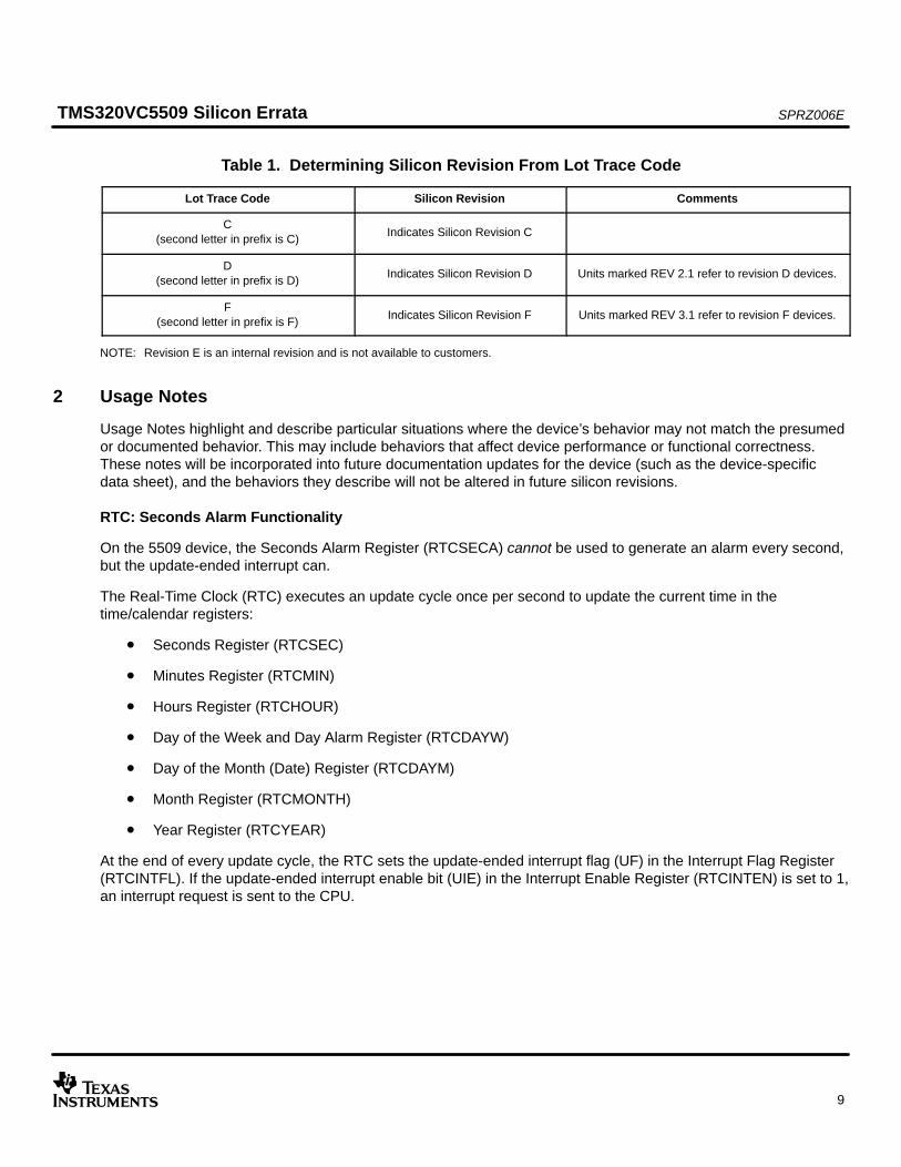
The device revision can be determined by the lot trace code marked on the top of the package. The locations forthe lot trace codes for the PGE and the GHH packages are shown in Figure 1 and Figure 2, respectively. Thelocation of other markings may vary per device. Table 1 shows how to determine the silicon revision from the lottrace code.
Qualified devices in the PGE package are marked with the letters “TMS” at the beginning of the device name, whilenonqualified devices in the PGE package are marked with the letters “TMX” or “TMP” at the beginning of thedevice name. Similarly, qualified devices in the GHH package are marked with the letters “DV” at the beginning ofthe device name, and nonqualified devices in the GHH package are marked with the letters “XDV” or “PDV” at thebeginning of the device name.
DSP
Lot trace code with D
PGE100TMS320VC5509
ED−YMLLLLW
Figure 1. Example, Typical Lot Trace Code for TMS320VC5509 (PGE)
PDVC5509GHH100
ED−YMLLLLW
Figure 2. Example, Typical Lot Trace Code for TMS320VC5509 (GHH)
SPRZ006ETMS320VC5509 Silicon Errata
9
Table 1. Determining Silicon Revision From Lot Trace Code
Lot Trace Code Silicon Revision Comments
C(second letter in prefix is C)
Indicates Silicon Revision C
D(second letter in prefix is D)
Indicates Silicon Revision D Units marked REV 2.1 refer to revision D devices.
F(second letter in prefix is F)
Indicates Silicon Revision F Units marked REV 3.1 refer to revision F devices.
NOTE: Revision E is an internal revision and is not available to customers.
2 Usage Notes
Usage Notes highlight and describe particular situations where the device’s behavior may not match the presumedor documented behavior. This may include behaviors that affect device performance or functional correctness.These notes will be incorporated into future documentation updates for the device (such as the device-specificdata sheet), and the behaviors they describe will not be altered in future silicon revisions.
RTC: Seconds Alarm Functionality
On the 5509 device, the Seconds Alarm Register (RTCSECA) cannot be used to generate an alarm every second,but the update-ended interrupt can.
The Real-Time Clock (RTC) executes an update cycle once per second to update the current time in thetime/calendar registers:
• Seconds Register (RTCSEC)
• Minutes Register (RTCMIN)
• Hours Register (RTCHOUR)
• Day of the Week and Day Alarm Register (RTCDAYW)
• Day of the Month (Date) Register (RTCDAYM)
• Month Register (RTCMONTH)
• Year Register (RTCYEAR)
At the end of every update cycle, the RTC sets the update-ended interrupt flag (UF) in the Interrupt Flag Register(RTCINTFL). If the update-ended interrupt enable bit (UIE) in the Interrupt Enable Register (RTCINTEN) is set to 1,an interrupt request is sent to the CPU.
SPRZ006ETMS320VC5509 Silicon Errata
10
3 Known Design Marginality/Exceptions to Functional Specifications
3.1 Summary of Advisories
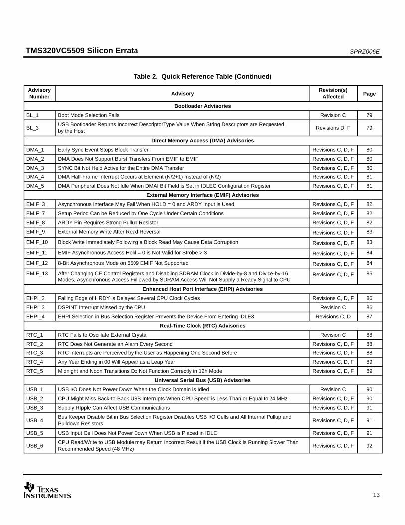
Table 2 provides a quick reference of all advisories by number, silicon revision affected, and lists their respectivepage location.
Table 2. Quick Reference Table
AdvisoryNumber Advisory
Revision(s)Affected Page
CPU Advisories
CPU_1 While Repeat Instruction Not Implemented Revisions C, D, F 15
CPU_2 Modification of Block Repeat Count Registers Not Pipeline-Protected Revisions C, D, F 15
CPU_3 Branch Out of an Active Block Repeat Revisions C, D, F 16
CPU_4 Limited Parallelization of Single Memory Operand Instructions Revisions C, D, F 17
CPU_5 IVPD Not Pipeline-Protected Against RESET, INTR, or TRAP Instructions Revisions C, D, F 17
CPU_6 Pending Interrupts During Wake-up From IDLE Revisions C, D, F 18
CPU_7 Modification of Extended 7 Bits of Auxiliary Registers is Not Pipeline-Protected Revisions C, D, F 18
CPU_8 SP Modification in 32-Bit Stack Mode Followed by SSP Move is Not Pipeline-Protected Revisions C, D, F 19
CPU_9 Nonparallel D-Unit Swap Executed Conditionally Does Not Null Execution Correctly Revisions C, D, F 20
CPU_10 Accumulator Use by AU or in Program Control Flow Paralleled With an Accumulator Move Revisions C, D, F 20
CPU_11 A-Unit SWAP in Parallel With D-Unit SWAP Revisions C, D, F 21
CPU_12 Accumulator SWAP in Parallel With the Accumulator Modification Revisions C, D, F 21
CPU_13 Dual-Write to the Same Address With a Bypass Read From the Same Address in Memory Revisions C, D, F 22
CPU_14 Parallel Register Comparison and Move Execution Involving A-Unit / D-Unit Revisions C, D, F 22
CPU_15 Dual Push of TAx and ACx Registers Not Pipeline-Protected Revisions C, D, F 23
CPU_16 Parallel Operation of a Push and Pop of an Extended Addressing Register Revisions C, D, F 23
CPU_17 Parallel Operation of Extended Register Load With a 16-bit Address/Data Register Load Revisions C, D, F 24
CPU_20 Compare and Branch Instruction in 40-Bit ALU Can Return Wrong Comparison Result Revisions C, D, F 25
CPU_21 Bit Test/Modify to/from I/O Space Via Parallel Execution Revisions C, D, F 26
CPU_22 Dual-Read or Dual-Write With Readport() or Writeport() Qualifier Revisions C, D, F 27
CPU_23 Parallel Execution of a Program Unit Store With Any Other Memory Store Revisions C, D, F 27
CPU_24 TCx Bit Corrupted by Single Register Comparison Instruction Revisions C, D, F 28
CPU_25 Conditional Return Paralleled With Memory Store Revisions C, D, F 29
CPU_26 E-Bus Write Data Corrupted When AC3 Load in Parallel With E-Bus Write Instruction Revisions C, D, F 29
CPU_27 Smem Push/Pop Instructions Fail When Smem is *port(#k16) Revisions C, D, F 30
CPU_28 MAR Instruction Using T0 May Fail When the C54CM Bit is Set (=1) Revisions C, D, F 30
CPU_29 Move Instructions Referencing Cmem and Smem Using the *port(#k16) Modifier Revisions C, D, F 31
CPU_30 Interrupt During Conditional Execution Instruction Sequence Corrupts Program Counter Revisions C, D, F 32
CPU_31 AR3 Update Not Pipeline-Protected After BK03 Write When AR3LC = 1 Revisions C, D, F 33
CPU_32 Parallel Execution of Register Bit Pair Test Instruction Revisions C, D, F 33
CPU_33 SATD Causes Saturation on Logical Shifts With AND, OR, and XOR Instructions Revisions C, D, F 34
CPU_34 Byte Write Followed by Word or Long-Word Read Not Pipeline-Protected Revisions C, D, F 34
SPRZ006ETMS320VC5509 Silicon Errata
11
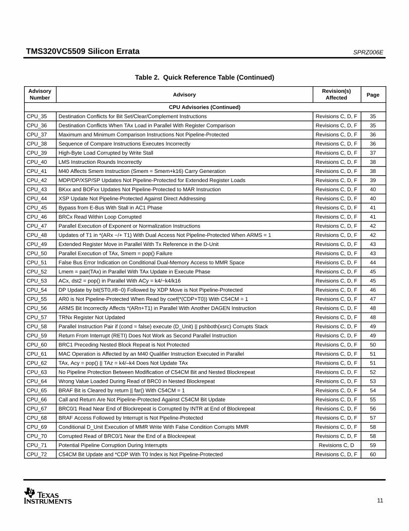
Table 2. Quick Reference Table (Continued)
AdvisoryNumber Page
Revision(s)AffectedAdvisory
CPU Advisories (Continued)
CPU_35 Destination Conflicts for Bit Set/Clear/Complement Instructions Revisions C, D, F 35
CPU_36 Destination Conflicts When TAx Load in Parallel With Register Comparison Revisions C, D, F 35
CPU_37 Maximum and Minimum Comparison Instructions Not Pipeline-Protected Revisions C, D, F 36
CPU_38 Sequence of Compare Instructions Executes Incorrectly Revisions C, D, F 36
CPU_39 High-Byte Load Corrupted by Write Stall Revisions C, D, F 37
CPU_40 LMS Instruction Rounds Incorrectly Revisions C, D, F 38
CPU_41 M40 Affects Smem Instruction (Smem = Smem+k16) Carry Generation Revisions C, D, F 38
CPU_42 MDP/DP/XSP/SP Updates Not Pipeline-Protected for Extended Register Loads Revisions C, D, F 39
CPU_43 BKxx and BOFxx Updates Not Pipeline-Protected to MAR Instruction Revisions C, D, F 40
CPU_44 XSP Update Not Pipeline-Protected Against Direct Addressing Revisions C, D, F 40
CPU_45 Bypass from E-Bus With Stall in AC1 Phase Revisions C, D, F 41
CPU_46 BRCx Read Within Loop Corrupted Revisions C, D, F 41
CPU_47 Parallel Execution of Exponent or Normalization Instructions Revisions C, D, F 42
CPU_48 Updates of T1 in *(ARx −/+ T1) With Dual Access Not Pipeline-Protected When ARMS = 1 Revisions C, D, F 42
CPU_49 Extended Register Move in Parallel With Tx Reference in the D-Unit Revisions C, D, F 43
CPU_50 Parallel Execution of TAx, Smem = pop() Failure Revisions C, D, F 43
CPU_51 False Bus Error Indication on Conditional Dual-Memory Access to MMR Space Revisions C, D, F 44
CPU_52 Lmem = pair(TAx) in Parallel With TAx Update in Execute Phase Revisions C, D, F 45
CPU_53 ACx, dst2 = pop() in Parallel With ACy = k4/−k4/k16 Revisions C, D, F 45
CPU_54 DP Update by bit(ST0,#8−0) Followed by XDP Move is Not Pipeline-Protected Revisions C, D, F 46
CPU_55 AR0 is Not Pipeline-Protected When Read by coef(*(CDP+T0)) With C54CM = 1 Revisions C, D, F 47
CPU_56 ARMS Bit Incorrectly Affects *(ARn+T1) in Parallel With Another DAGEN Instruction Revisions C, D, F 48
CPU_57 TRNx Register Not Updated Revisions C, D, F 48
CPU_58 Parallel Instruction Pair if (cond = false) execute (D_Unit) || pshboth(xsrc) Corrupts Stack Revisions C, D, F 49
CPU_59 Return From Interrupt (RETI) Does Not Work as Second Parallel Instruction Revisions C, D, F 49
CPU_60 BRC1 Preceding Nested Block Repeat is Not Protected Revisions C, D, F 50
CPU_61 MAC Operation is Affected by an M40 Qualifier Instruction Executed in Parallel Revisions C, D, F 51
CPU_62 TAx, Acy = pop() || TAz = k4/–k4 Does Not Update TAx Revisions C, D, F 51
CPU_63 No Pipeline Protection Between Modification of C54CM Bit and Nested Blockrepeat Revisions C, D, F 52
CPU_64 Wrong Value Loaded During Read of BRC0 in Nested Blockrepeat Revisions C, D, F 53
CPU_65 BRAF Bit is Cleared by return || far() With C54CM = 1 Revisions C, D, F 54
CPU_66 Call and Return Are Not Pipeline-Protected Against C54CM Bit Update Revisions C, D, F 55
CPU_67 BRC0/1 Read Near End of Blockrepeat is Corrupted by INTR at End of Blockrepeat Revisions C, D, F 56
CPU_68 BRAF Access Followed by Interrupt is Not Pipeline-Protected Revisions C, D, F 57
CPU_69 Conditional D_Unit Execution of MMR Write With False Condition Corrupts MMR Revisions C, D, F 58
CPU_70 Corrupted Read of BRC0/1 Near the End of a Blockrepeat Revisions C, D, F 58
CPU_71 Potential Pipeline Corruption During Interrupts Revisions C, D 59
CPU_72 C54CM Bit Update and *CDP With T0 Index is Not Pipeline-Protected Revisions C, D, F 60
SPRZ006ETMS320VC5509 Silicon Errata
12
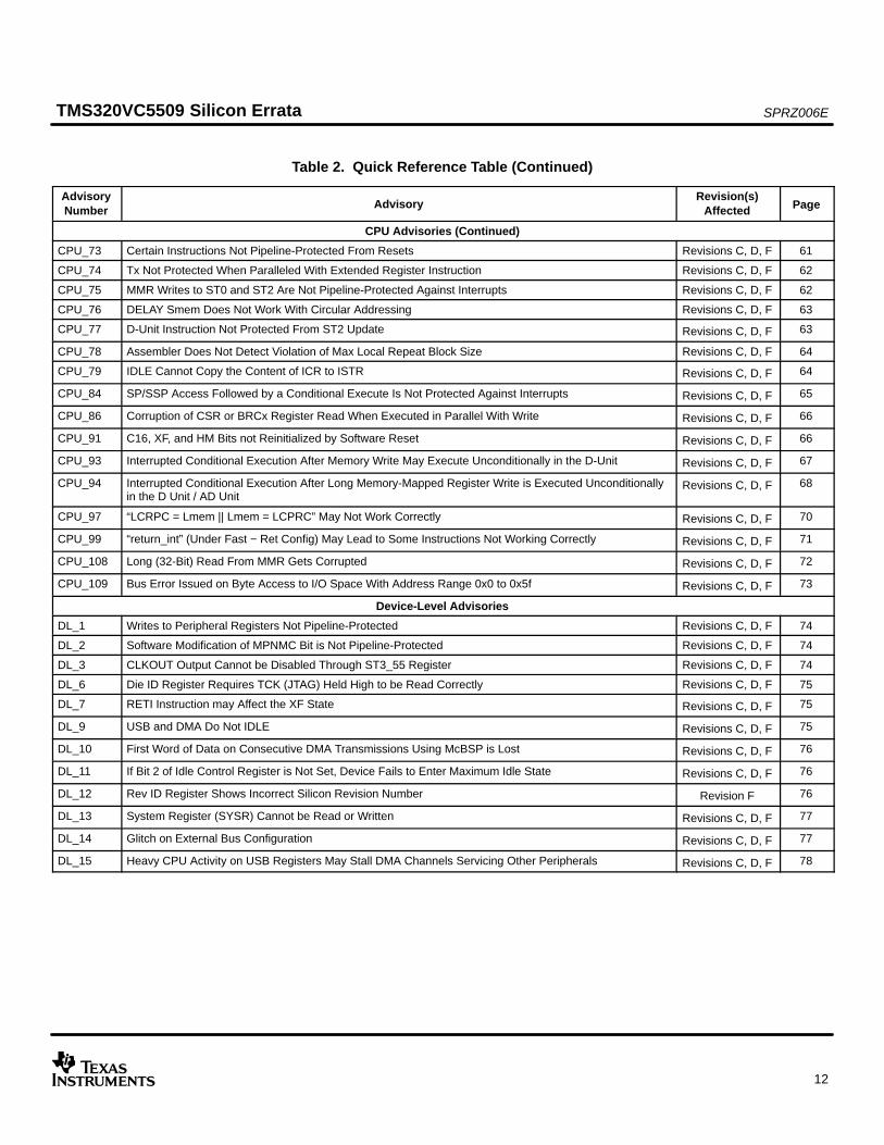
Table 2. Quick Reference Table (Continued)
AdvisoryNumber Page
Revision(s)AffectedAdvisory
CPU Advisories (Continued)
CPU_73 Certain Instructions Not Pipeline-Protected From Resets Revisions C, D, F 61
CPU_74 Tx Not Protected When Paralleled With Extended Register Instruction Revisions C, D, F 62
CPU_75 MMR Writes to ST0 and ST2 Are Not Pipeline-Protected Against Interrupts Revisions C, D, F 62
CPU_76 DELAY Smem Does Not Work With Circular Addressing Revisions C, D, F 63
CPU_77 D-Unit Instruction Not Protected From ST2 Update Revisions C, D, F 63
CPU_78 Assembler Does Not Detect Violation of Max Local Repeat Block Size Revisions C, D, F 64
CPU_79 IDLE Cannot Copy the Content of ICR to ISTR Revisions C, D, F 64
CPU_84 SP/SSP Access Followed by a Conditional Execute Is Not Protected Against Interrupts Revisions C, D, F 65
CPU_86 Corruption of CSR or BRCx Register Read When Executed in Parallel With Write Revisions C, D, F 66
CPU_91 C16, XF, and HM Bits not Reinitialized by Software Reset Revisions C, D, F 66
CPU_93 Interrupted Conditional Execution After Memory Write May Execute Unconditionally in the D-Unit Revisions C, D, F 67
CPU_94 Interrupted Conditional Execution After Long Memory-Mapped Register Write is Executed Unconditionallyin the D Unit / AD Unit
Revisions C, D, F 68
CPU_97 “LCRPC = Lmem || Lmem = LCPRC” May Not Work Correctly Revisions C, D, F 70
CPU_99 “return_int” (Under Fast − Ret Config) May Lead to Some Instructions Not Working Correctly Revisions C, D, F 71
CPU_108 Long (32-Bit) Read From MMR Gets Corrupted Revisions C, D, F 72
CPU_109 Bus Error Issued on Byte Access to I/O Space With Address Range 0x0 to 0x5f Revisions C, D, F 73
Device-Level Advisories
DL_1 Writes to Peripheral Registers Not Pipeline-Protected Revisions C, D, F 74
DL_2 Software Modification of MPNMC Bit is Not Pipeline-Protected Revisions C, D, F 74
DL_3 CLKOUT Output Cannot be Disabled Through ST3_55 Register Revisions C, D, F 74
DL_6 Die ID Register Requires TCK (JTAG) Held High to be Read Correctly Revisions C, D, F 75
DL_7 RETI Instruction may Affect the XF State Revisions C, D, F 75
DL_9 USB and DMA Do Not IDLE Revisions C, D, F 75
DL_10 First Word of Data on Consecutive DMA Transmissions Using McBSP is Lost Revisions C, D, F 76
DL_11 If Bit 2 of Idle Control Register is Not Set, Device Fails to Enter Maximum Idle State Revisions C, D, F 76
DL_12 Rev ID Register Shows Incorrect Silicon Revision Number Revision F 76
DL_13 System Register (SYSR) Cannot be Read or Written Revisions C, D, F 77
DL_14 Glitch on External Bus Configuration Revisions C, D, F 77
DL_15 Heavy CPU Activity on USB Registers May Stall DMA Channels Servicing Other Peripherals Revisions C, D, F 78
SPRZ006ETMS320VC5509 Silicon Errata
13
Table 2. Quick Reference Table (Continued)
AdvisoryNumber Page
Revision(s)AffectedAdvisory
Bootloader Advisories
BL_1 Boot Mode Selection Fails Revision C 79
BL_3USB Bootloader Returns Incorrect DescriptorType Value When String Descriptors are Requestedby the Host
Revisions D, F 79
Direct Memory Access (DMA) Advisories
DMA_1 Early Sync Event Stops Block Transfer Revisions C, D, F 80
DMA_2 DMA Does Not Support Burst Transfers From EMIF to EMIF Revisions C, D, F 80
DMA_3 SYNC Bit Not Held Active for the Entire DMA Transfer Revisions C, D, F 80
DMA_4 DMA Half-Frame Interrupt Occurs at Element (N/2+1) Instead of (N/2) Revisions C, D, F 81
DMA_5 DMA Peripheral Does Not Idle When DMAI Bit Field is Set in IDLEC Configuration Register Revisions C, D, F 81
External Memory Interface (EMIF) Advisories
EMIF_3 Asynchronous Interface May Fail When HOLD = 0 and ARDY Input is Used Revisions C, D, F 82
EMIF_7 Setup Period Can be Reduced by One Cycle Under Certain Conditions Revisions C, D, F 82
EMIF_8 ARDY Pin Requires Strong Pullup Resistor Revisions C, D, F 82
EMIF_9 External Memory Write After Read Reversal Revisions C, D, F 83
EMIF_10 Block Write Immediately Following a Block Read May Cause Data Corruption Revisions C, D, F 83
EMIF_11 EMIF Asynchronous Access Hold = 0 is Not Valid for Strobe > 3 Revisions C, D, F 84
EMIF_12 8-Bit Asynchronous Mode on 5509 EMIF Not Supported Revisions C, D, F 84
EMIF_13 After Changing CE Control Registers and Disabling SDRAM Clock in Divide-by-8 and Divide-by-16Modes, Asynchronous Access Followed by SDRAM Access Will Not Supply a Ready Signal to CPU
Revisions C, D, F 85
Enhanced Host Port Interface (EHPI) Advisories
EHPI_2 Falling Edge of HRDY is Delayed Several CPU Clock Cycles Revisions C, D, F 86
EHPI_3 DSPINT Interrupt Missed by the CPU Revision C 86
EHPI_4 EHPI Selection in Bus Selection Register Prevents the Device From Entering IDLE3 Revisions C, D 87
Real-Time Clock (RTC) Advisories
RTC_1 RTC Fails to Oscillate External Crystal Revision C 88
RTC_2 RTC Does Not Generate an Alarm Every Second Revisions C, D, F 88
RTC_3 RTC Interrupts are Perceived by the User as Happening One Second Before Revisions C, D, F 88
RTC_4 Any Year Ending in 00 Will Appear as a Leap Year Revisions C, D, F 89
RTC_5 Midnight and Noon Transitions Do Not Function Correctly in 12h Mode Revisions C, D, F 89
Universal Serial Bus (USB) Advisories
USB_1 USB I/O Does Not Power Down When the Clock Domain is Idled Revision C 90
USB_2 CPU Might Miss Back-to-Back USB Interrupts When CPU Speed is Less Than or Equal to 24 MHz Revisions C, D, F 90
USB_3 Supply RIpple Can Affect USB Communications Revisions C, D, F 91
USB_4Bus Keeper Disable Bit in Bus Selection Register Disables USB I/O Cells and All Internal Pullup andPulldown Resistors
Revisions C, D, F 91
USB_5 USB Input Cell Does Not Power Down When USB is Placed in IDLE Revisions C, D, F 91
USB_6CPU Read/Write to USB Module may Return Incorrect Result if the USB Clock is Running Slower ThanRecommended Speed (48 MHz)
Revisions C, D, F 92
SPRZ006ETMS320VC5509 Silicon Errata
14
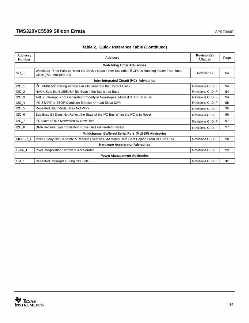
Table 2. Quick Reference Table (Continued)
AdvisoryNumber Page
Revision(s)AffectedAdvisory
Watchdog Timer Advisories
WT_1Watchdog Timer Fails to Reset the Device Upon Timer Expiration if CPU is Running Faster Than InputClock (PLL Multiplier >1)
Revision C 93
Inter-Integrated Circuit (I2C) Advisories
I2C_1 I2C 10-Bit Addressing Access Fails to Generate the Correct Clock Revisions C, D, F 94
I2C_2 NACK Sets the BUSBUSY Bit, Even if the Bus is not Busy Revisions C, D, F 94
I2C_3 ARDY Interrupt is not Generated Properly in Non-Repeat Mode if STOP Bit is Set Revisions C, D, F 94
I2C_4 I2C START or STOP Condition Empties Unread Slave DXR Revisions C, D, F 95
I2C_5 Repeated Start Mode Does Not Work Revisions C, D, F 96
I2C_6 Bus Busy Bit Does Not Reflect the State of the I2C Bus When the I2C is in Reset Revisions C, D, F 96
I2C_7 I2C Slave DRR Overwritten by New Data Revisions C, D, F 97
I2C_8 DMA Receive Synchronization Pulse Gets Generated Falsely Revisions C, D, F 97
Multichannel Buffered Serial Port (McBSP) Advisories
MCBSP_1 McBSP May Not Generate a Receive Event to DMA When Data Gets Copied From RSR to DRR Revisions C, D, F 98
Hardware Accelerator Advisories
HWA_1 Pixel Interpolation Hardware Accelerator Revisions C, D, F 99
Power Management Advisories
PM_1 Repeated Interrupts During CPU Idle Revisions C, D, F 101

SPRZ006ETMS320VC5509 Silicon Errata
15
3.2 CPU Advisories
While Repeat Instruction Not ImplementedAdvisory CPU_1
Revision(s) Affected: Revisions C, D, and F
Details: The while repeat (cond && (RPTC & k8)) Instruction has not been implemented in 5509Revisions C, D, and F. This instruction will be included in a future revision of the device.
Assembler Notification: The assembler (versions 1.60 and later) will generate a REMARK when this instruction is usedif Revisions C, D, and F silicon target is specified.
Workaround: This instruction is supported in the VC5509 simulator. It can be used for code development forfuture 5509 silicon revisions, but should be avoided in code intended to run on Revisions C, D,and F silicon.
Modification of Block Repeat Count Registers Not Pipeline-ProtectedAdvisory CPU_2
Revision(s) Affected: Revisions C, D, and F
Details: The pipeline protection for the block repeat count registers (BRC0, BRC1, and BRS1) havenot been fully implemented for the count registers supporting block repeat operations. IfBRC0, BRC1 or BRS1 are modified inside an active block repeat loop, these registers maybecome corrupted if modified when there are less than seven cycles plus 16 bytes before theend of the block repeat. This requirement is applied to the repeat block and its associatedcount register. Example: BRC0 for the outer loop, BRC1 for the inner loop.
Assembler Notification: The assembler (revisions 1.70 and later) will generate a REMARK if it finds a modification ofthe above registers within a repeat block.
Workaround: Modification of these registers within an active block repeat should be avoided unless sevencycles plus 16 bytes can be specified between the register modification and the end of theblock repeat. Be aware that active interrupts (and the returns from interrupt service routines)can alter block repeat loop timings and cause the seven cycle plus 16-byte requirement to beviolated. To protect against this occurrence, the block repeat registers affected should not bemodified inside an interrupt service routine.

SPRZ006ETMS320VC5509 Silicon Errata
16
Branch Out of an Active Block RepeatAdvisory CPU_3
Revision(s) Affected: Revisions C, D, and F
Details: When the C54CM mode bit is set to 1, program discontinuities (branch) from within an activerepeat block to a destination within five bytes from the end of the repeat block may fail.
Example:Blockrepeat: . goto Label .Label:
Assembler Notification: The assembler (versions 1.70 and later) will attempt to determine if a branch occurs within arepeat block to outside the repeat block, and if so, will generate a remark for all labels withinfive bytes of that end of the block.
Workaround: Maintain at least five bytes of code between the end of the block repeat and the target of thebranch. This can be useful code or NOPs.
Example:Blockrepeat: . goto Label nop nop nop nop nopLabel:

SPRZ006ETMS320VC5509 Silicon Errata
17
Limited Parallelization of Single Memory Operand InstructionsAdvisory CPU_4
Revision(s) Affected: Revisions C, D, and F
Details: Parallel operation of single memory operand instructions (Instruction1 || Instruction 2) is notyet supported when both of the following are true:
• Instruction 1 is any of the following instructions:TC1 = bit(Smem,k4), bit(Smem,k4) = #1 (algebraic assembly examples)TC2 = bit(Smem,k4), bit(Smem,k4) = #1TC1 = bit(Smem,k4), bit(Smem,k4) = #0TC2 = bit(Smem,k4), bit(Smem,k4) = #0TC1 = bit(Smem,k4), cbit(Smem,k4)TC2 = bit(Smem,k4), cbit(Smem,k4)bit(Smem,src) = #1bit(Smem,src) = #0cbit(Smem,src)Smem = Smem & k16 (logical AND)Smem = Smem | k16 (logical OR)Smem = Smem ^ k16 (logical XOR)Smem = Smem + k16 (logical AND)
• Instruction 2 is any single memory operand write instruction
Assembler Notification: Assembler will detect this condition and reject this form of parallelism for Revisions C, D, andF silicon.
Workaround: These instructions should not be executed in parallel. They can be executed sequentially withcorrect results.
IVPD Not Pipeline-Protected Against RESET, INTR, or TRAP InstructionsAdvisory CPU_5
Revision(s) Affected: Revisions C, D, and F
Details: If the DSP Interrupt vector pointer (IVPD) register is modified prior to execution of a RESET,INTR or TRAP instruction, the pipeline does not ensure that the vector pointer modification ismade before the instructions are executed.
Assembler Notification: None
Workaround: Maintain at least seven cycles (either or useful code or NOPs) between modifications of theIVPD registers and execution of the RESET, INTR or TRAP instructions to allow the registermodifications to complete the execute phase of the pipeline.

SPRZ006ETMS320VC5509 Silicon Errata
18
Pending Interrupts During Wake-up From IDLEAdvisory CPU_6
Revision(s) Affected: Revisions C, D, and F
Details: If the IDLE instruction is decoded while an interrupt is pending (an interrupt flag set in the IFRand the INTM bit is set), there will be a null cycle in the pipeline between the execution of theIDLE instruction and the instruction that follows it. The only effect of this behavior is that theinstructions following the IDLE will execute one cycle later than if no interrupts were pending.There are no other effects on the accuracy of the surrounding code.
Assembler Notification: None
Workaround: Not applicable. There is no impact to customer functionality.
Modification of Extended 7 Bits of Auxiliary Registers is Not Pipeline-ProtectedAdvisory CPU_7
Revision(s) Affected: Revisions C, D, and F
Details: If an instruction performing an extended address register read in the execute phase of thepipeline is followed by an instruction that modifies the same extended address register in theaddress phase, then the destination of the first instruction will not be loaded with the correctvalue.
Algebraic assembly example:XAR1 = XAR0XAR0 = #0x123456
Mnemonic assembly example:MOV XAR0, XAR1AMAR *(#k),XAR0
Assembler Notification: Assembler (versions 1.70 and later) will attempt to recognize occurrences of this issue andgenerate a WARNING.
Workaround: At least three cycles (either useful code or NOPs) should be inserted between the registerupdate in the address phase and the address register update in the execute phase.Alternatively, complete all extended address register updates to the address phase of thepipeline.
Workaround examples:MOV XAR0, XAR1<instruction><instruction><instruction>AMAR *(#k), XAR0
orAMOV XAR0, XAR1AMAR *(#k), XAR0

SPRZ006ETMS320VC5509 Silicon Errata
19
SP Modification in 32-Bit Stack Mode Followed by SSP Move is Not Pipeline-ProtectedAdvisory CPU_8
Revision(s) Affected: Revisions C, D, and F
Details: If an instruction that modifies the user stack pointer (SP) [which also automatically updates thesystem stack pointer (SSP) in 32-bit stack mode] is followed immediately by either amemory-mapped register access to the SSP, or an instruction access to the SSP, the contentsof the destination register will be incorrect. This sequence is illustrated in the code examplebelow:
Algebraic assembly example:SP = SP − #30AR2 = SSP
Mnemonic assembly example:AADD #(−30),SPMOV SSP,AR2
In this example, the resulting contents of AR2 will be the old SSP value, not the updatedvalue.
Assembler Notification: Assembler (versions 1.70 and later) will attempt to identify this problem and generatean ERROR.
Workaround: Instruction accesses of the SSP in 32-bit stack mode – Place one instruction or NOP betweenthe stack modification and the access to the system stack pointer. In addition, interruptsshould be prevented (disabled) during this three instruction sequence because the interruptcould cause the context to be saved when the SP has been updated but the SSP has not yetbeen updated.
Mnemonic assembly workaround example:AADD #(−30),SPNOPMOV SSP,AR2
MMR register accesses (using the mmap qualifier) of the SSP in 32-bit stack mode – Placetwo instructions or NOPs between the stack modification and the access to the system stackpointer. In addition, interrupts should be prevented (disabled) during this three instructionsequence because the interrupt could cause the context to be saved when the SP has beenupdated but the SSP has not yet been updated.
Mnemonic assembly workaround example:AADD #(−30),SPNOPNOPMOV SSP,Smem || mmap
Or
Use the dual 16-bit stack mode. This exception only occurs in 32-bit stack mode. In 16-bitstack mode, the stack operation is correct with the following considerations:
• Use of the dual 16-bit stack mode may create issues with operations that utilize stackunwinding techniques.
• Dual 16-bit mode may create incorrect operation of 54x code if the code is using far callsand the called routine uses stack relative data addressing.

SPRZ006ETMS320VC5509 Silicon Errata
20
Nonparallel D-Unit Swap Executed Conditionally Does Not Null Execution CorrectlyAdvisory CPU_9
Revision(s) Affected: Revisions C, D, and F
Details: If a conditional execution instruction operating on the D-Unit is followed by a SWAPinstruction, the conditional execution will not terminate the execution of the SWAP instruction ifthe condition is false (the SWAP instruction will always be performed regardless of the state ofthe condition).
Algebraic assembly example:If (cond) execute (D_Unit)Swap (src,dst)
Assembler Notification: Assembler (versions 1.70 and later) will generate an error for Revisions C, D, and F silicon.
Workaround: Generate the conditional execution of the D unit swap in a single cycle operation. The codesequence is as follows:If (cond) execute (D_Unit) || Swap (src,dst)
Accumulator Use by AU or in Program Control Flow Paralleled With an Accumulator MoveAdvisory CPU_10
Revision(s) Affected: Revisions C, D, and F
Details: Case 1 – Accumulator used in AU:
If an instruction that uses an accumulator value in the AU is paralleled with an accumulatormove referencing the same accumulator, the accumulator move may fail.
Algebraic assembly example:AR2 = HI(AC0) || AC0 = AC1
Case 2 – Accumulator used in control flow:
If an instruction that uses an accumulator value to affect program control flow is paralleled withan accumulator move referencing the same accumulator, the accumulator move may fail.
Algebraic assembly example:goto AC0 || AC0 = AC1
Assembler Notification: Assembler (versions 2.03 and later) will generate an error for Revisions C, D, and F silicon.
Workaround: For both cases, the workaround is not to execute these instructions in parallel. Executedsequentially, the instructions will perform correctly.

SPRZ006ETMS320VC5509 Silicon Errata
21
A-Unit SWAP in Parallel With D-Unit SWAPAdvisory CPU_11
Revision(s) Affected: Revisions C, D, and F
Details: If a SWAP instruction used to swap A-Unit registers is paralleled with a SWAP instruction thatattempts to swap D-Unit registers, the code may fail.
Algebraic assembly example:SWAP (AC1, AC3) || SWAP (AR1, AR0)
Assembler Notification: Assembler (versions 1.70 and later) will detect this and reject this form of parallelism forRevisions C, D, and F silicon.
Workaround: These instructions should not be executed in parallel. If executed sequentially, the codeperforms as expected.
Accumulator SWAP in Parallel With the Accumulator ModificationAdvisory CPU_12
Revision(s) Affected: Revisions C, D, and F
Details: If the SWAP instruction used to swap accumulators is paralleled with an instruction thatattempts to modify the contents of one of the accumulators referenced in the SWAP, the codemay fail.
Algebraic assembly example:SWAP(AC1, AC3) || AC1 = #1234
Assembler Notification: Assembler (versions 1.70 and later) will attempt to detect this and reject this form ofparallelism for Revisions C, D, and F silicon.
Workaround: These instructions should not be executed in parallel. If executed sequentially, the codeperforms as expected.

SPRZ006ETMS320VC5509 Silicon Errata
22
Dual-Write to the Same Address With a Bypass Read From the Same Address in MemoryAdvisory CPU_13
Revision(s) Affected: Revisions C, D, and F
Details: This is an advisory case and is a condition that would not be expected in a user’s code (sinceboth writes are directed to the same address). This advisory is included to project a completelist of projected functional changes.
On the 55x architecture, if a write is made to a memory location and in the same cycle a readis performed to the same memory location, the architecture employs a bypass readmechanism to optimize pipeline cycles. In a bypass read, the value to be written to memory isread directly from the bus as the write is being performed. This prevents additional pipelinecycles that would be incurred if the read were forced to wait for the write to be completed.
If, during the same cycle, a dual-write operation addresses the same memory location fromthe CPU using the E and F busses and a read of this memory location is requested by theCPU, different values are loaded into the memory location and returned to the CPU. Thememory location is loaded with the value that was on the F bus and the value on the E bus isbypassed from the write and returned from the CPU.
Correction in a future revision will be to insure the values match.
Assembler Notification: None
Workaround: In a dual-write operation (two 16-bit writes), the destination should not be the same location.This is an unsupported operation.
Parallel Register Comparison and Move Execution Involving A-Unit / D-UnitAdvisory CPU_14
Revision(s) Affected: Revisions C, D, and F
Details: Parallel execution of the form:TCx = uns(src relop dst) || Instruction2
will fail under the following conditions:• src is a TAx register• Instruction2 is any D-Unit instruction that references a TAy register
Instruction2 will be incorrectly calculated using the TAx value instead of the TAy value.
Algebraic example:TC1 = (AR1 < AC1) || AC2 = AC2 + AR2 ; Will compute as AC2 = AC2 + AR1
Assembler Notification: Assembler (versions 1.80 and later) will detect this and reject this form of parallelism forRevisions C, D, and F silicon.
Workaround: Do not use these instructions in parallel, or use the TAx register in the register compareinstruction as the dst instead of the src if possible.
Instead of:TC1 = (AR1 == AC1) || AC2 = AC2 + AR2
Use:TC1 = (AC1 == AR1) || AC2 = AC2 + AR2

SPRZ006ETMS320VC5509 Silicon Errata
23
Dual Push of TAx and ACx Registers Not Pipeline-ProtectedAdvisory CPU_15
Revision(s) Affected: Revisions C, D, and F
Details: When a dual push instruction combining an A-unit source and a D-unit source (accumulator) isfollowed by an instruction that updates an A-unit register in the address phase of the pipeline,the update to the A-unit register in the second instruction is not Pipeline-Protected.
Example:PSH AR0, AC0AMAR #12, AR0
Assembler Notification: Assembler (versions 1.70 and later) will detect this and reject this form of parallelism forRevisions C, D, and F silicon.
Workaround: At least three cycles (either useful code or NOPs) should be inserted between the twoinstructions.
Parallel Operation of a Push and Pop of an Extended Addressing RegisterAdvisory CPU_16
Revision(s) Affected: Revisions C, D, and F
Details: The parallel operation of any instruction with a push to or pop from an extended addressingregister (XARn, XDP, XCDP) is not supported in Revisions C, D, and F silicon.
Examples:<instruction> || Pushboth XAR0
or<instruction> || Popboth XAR1
Assembler Notification: Assembler (versions 1.70 and later) will detect this and reject this form of parallelism forRevisions C, D, and F silicon.
Workaround: Do not use the parallel execution for these instructions.
SPRZ006ETMS320VC5509 Silicon Errata
24
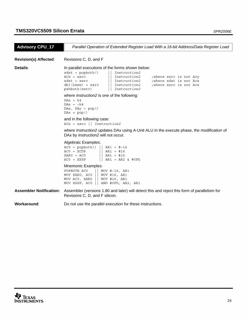
Parallel Operation of Extended Register Load With a 16-bit Address/Data Register LoadAdvisory CPU_17
Revision(s) Affected: Revisions C, D, and F
Details: In parallel executions of the forms shown below:xdst = popboth() || Instruction2ACx = xsrc || Instruction2 ;where xsrc is not Acyxdst = xsrc || Instruction2 ;where xdst is not Acxdbl(Lmem) = xsrc || Instruction2 ;where xsrc is not Acxpshboth(xsrc) || Instruction2
where Instruction2 is one of the following:DAx = k4DAx = −k4DAx, DAy = pop()DAx = pop()
and in the following case:ACx = xsrc || Instruction2
where Instruction2 updates DAx using A-Unit ALU in the execute phase, the modification ofDAx by Instruction2 will not occur.
Algebraic Examples:AC0 = popboth() || AR1 = #−16AC0 = XCDP || AR1 = #16XAR0 = AC0 || AR1 = #16AC0 = XSSP || AR1 = AR2 & #0Fh
Mnemonic Examples:POPBOTH AC0 || MOV #−16, AR1MOV XAR0, AC0 || MOV #16, AR1MOV AC0, XAR0 || MOV #16, AR1MOV XSSP, AC0 || AND #0Fh, AR2, AR1
Assembler Notification: Assembler (versions 1.80 and later) will detect this and reject this form of parallelism forRevisions C, D, and F silicon.
Workaround: Do not use the parallel execution for these instructions.
SPRZ006ETMS320VC5509 Silicon Errata
25
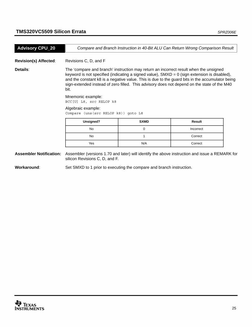
Compare and Branch Instruction in 40-Bit ALU Can Return Wrong Comparison ResultAdvisory CPU_20
Revision(s) Affected: Revisions C, D, and F
Details: The ‘compare and branch’ instruction may return an incorrect result when the unsignedkeyword is not specified (indicating a signed value), SMXD = 0 (sign extension is disabled),and the constant k8 is a negative value. This is due to the guard bits in the accumulator beingsign-extended instead of zero filled. This advisory does not depend on the state of the M40bit.
Mnemonic example:BCC[U] L8, src RELOP k8
Algebraic example:Compare (uns(src RELOP k8)) goto L8
Unsigned? SXMD Result
No 0 Incorrect
No 1 Correct
Yes N/A Correct
Assembler Notification: Assembler (versions 1.70 and later) will identify the above instruction and issue a REMARK forsilicon Revisions C, D, and F.
Workaround: Set SMXD to 1 prior to executing the compare and branch instruction.
SPRZ006ETMS320VC5509 Silicon Errata
26
Bit Test/Modify to/from I/O Space Via Parallel ExecutionAdvisory CPU_21
Revision(s) Affected: Revisions C, D, and F
Details: Modifications of register values in I/O space of the form:Instruction1 || readport () or instruction1 || writeport ()
will fail if instruction1 is one of the following instructions:TC1 = bit(Smem,k4) , bit(Smem,k4) = #1TC2 = bit(Smem,k4) , bit(Smem,k4) = #1TC1 = bit(Smem,k4) , bit(Smem,k4) = #0TC2 = bit(Smem,k4) , bit(Smem,k4) = #0TC1 = bit(Smem,k4) , cbit(Smem,k4)TC2 = bit(Smem,k4) , cbit(Smem,k4)bit(Smem,src) = #1bit(Smem,src) = #0cbit(Smem,src)Smem = Smem & k16Smem = Smem | k16Smem = Smem ^ k16Smem = Smem + K16
The readport reference will read from I/O space but write to memory space instead of I/Ospace.
The writeport reference will write to I/O space but read from memory space instead of I/Ospace.
Assembler Notification: Assembler (versions 1.70 and later) will detect this and reject this form of parallelism forRevisions C, D, and F silicon.
Workaround: Use the following steps:
Step 1: Read contents of the peripheral register into memory space using a single memory readinstruction in parallel with the readport() qualifier.
Step 2: Modify the register data in memory space.
Step 3: Write the modified contents back to I/O space using a single memory write instructionin parallel with the writeport() qualifier.

SPRZ006ETMS320VC5509 Silicon Errata
27
Dual-Read or Dual-Write With Readport() or Writeport() QualifierAdvisory CPU_22
Revision(s) Affected: Revisions C, D, and F
Details: In the case of a dual-read instruction in parallel with the readport() qualifier, only the Xmemoperand is read. No request is generated to read the Ymem operand.
Mnemonic example:MOV Xmem, Ymem, ACx || readport()
Algebraic example:LO(ACx) = Xmem, HI(ACx)= Ymem || readport()
In the case of a dual-write instruction in parallel with the writeport() qualifier, only the Ymemoperand is written. No request is generated to write the Xmem operand.
Mnemonic example:MOV ACx, Xmem, Ymem || writeport()
Algebraic example:Xmem = LO(ACx),Ymem = HI(Acx) || writeport()
Assembler Notification: Assembler (versions 1.70 and later) will detect this and reject this form of parallelism forRevisions C, D, and F silicon.
Workaround: For dual reads, replace the dual-read with two single reads.
For dual writes, replace the dual-write with two single writes.
Parallel Execution of a Program Unit Store With Any Other Memory StoreAdvisory CPU_23
Revision(s) Affected: Revisions C, D, and F
Details: Parallel execution instructions of the following forms will fail due to write data corruption. Thisissue is stall sensitive and may not always occur.
Algebraic forms:Smem = CSR || (any memory store instruction)Smem = BRC0 || (any memory store instruction)Smem = BRC1 || (any memory store instruction)
Mnemonic forms:MOV CSR, Smem || (any memory store instruction)MOV BRC0, Smem || (any memory store instruction)MOV BRC1, Smem || (any memory store instruction)
Assembler Notification: Assembler (versions 1.70 and later) will detect this and reject this form of parallelism forRevisions C, D, and F silicon.
Workaround: Do not execute these instructions in parallel.

SPRZ006ETMS320VC5509 Silicon Errata
28
TCx Bit Corrupted by Single Register Comparison InstructionAdvisory CPU_24
Revision(s) Affected: Revisions C, D, and F
Details: The TCx status bit(s) are corrupted when an instruction sequence of the following form isexecuted:
(any instruction) || (an instruction using the ALU in the address unit)...
(single register comparison instruction)
where the single register compare instruction is any of the following forms:
Algebraic Mnemonic
TCx = uns(src RELOP dst) CMP[U] src RELOP dst, TCx
TCx = TCy & uns(src RELOP dst) CMPAND[U] src RELOP dst, TCy, TCx
TCx = !TCy & uns(src RELOP dst) CMPAND[U] src RELOP dst, !TCy, TCx
TCx = TCy | uns(src RELOP dst) CMPOR[U] src RELOP dst, TCy, TCx
TCx = !TCy | uns(src RELOP dst) CMPOR[U] src RELOP dst, !TCy, TCx
Corruption of the TCx result occurs as follows:
src dst effect
TAx TAx TCx is incorrect
ACx TAx TCx is incorrect
TAx ACx TCx is incorrect
ACx ACx TCx is incorrect
Mnemonic example:MOV *AR0, T0 || BSET #11, ST1_55
CMP TO != AR1, TC1
Assembler Notification: Assembler (versions 1.70 and later) will detect the single register compare instruction andissue a remark for 1.x silicon.
Workaround: Execute a NOP in parallel with the register comparison instruction as follows:
• (any instruction) || (an instruction using the ALU in the address unit)
• (single register comparison instruction) || nop
SPRZ006ETMS320VC5509 Silicon Errata
29
Conditional Return Paralleled With Memory StoreAdvisory CPU_25
Revision(s) Affected: Revisions C, D, and F
Details: If a conditional return is paralleled with a memory store instruction, the store will fail if thecondition evaluated for the return is false. The store should be completed regardless of thecondition of the return.
Mnemonic exampleRETCC cond || MOV *ar1, *ar3
Algebraic exampleif (cond) return || *ar3 = *ar1
Assembler Notification: Assembler (versions 1.70 and later) will detect and reject this form of parallelism for RevisionsC, D, and F silicon.
Workaround: Do not execute these instructions in parallel.
E-Bus Write Data Corrupted When AC3 Load in Parallel With E-Bus Write InstructionAdvisory CPU_26
Revision(s) Affected: Revisions C, D, and F
Details: Data written on the E-bus will be corrupted in the case of the following parallel execution form:Instruction1 || Instruction2
Where Instruction1 is a move instruction that loads AC3 with the contents of one of thefollowing: XARx, XSP, XSSP, XDP or XCDP and Instruction2 is any of the instructions that canbe placed in the second slot (for parallel execution) and performs writes using the E-bus, suchas:
• call L16
• push(src1,src2)
• pshboth(xsrc)
• push(src)
• dbl(push(ACx)).
Mnemonic exampleMOV XCDP, AC3 || PSH AR0
Algebraic exampleAC3 = XCDP || push(AR0)
Assembler Notification: Assembler versions 1.70 and later will detect this and reject this form of parallelism forRevisions C, D, and F silicon.
Workaround: Do not use parallel execution with AC3 load.
SPRZ006ETMS320VC5509 Silicon Errata
30
Smem Push/Pop Instructions Fail When Smem is *port(#k16)Advisory CPU_27
Revision(s) Affected: Revisions C, D, and F
Details: The following single memory operand push and pop instructions fail when the Smemaddressing mode is *port(#k16)
Algebraic Form Mnemonic Form
Smem = pop() POP Smem
dst, Smem = pop() POP dst, Smem
push(Smem) PSH Smem
push(src, Smem) PSH src, Smem
Assembler Notification: Assembler (versions 1.70 and later) will detect this and reject this addressing mode forRevisions C, D, and F silicon.
Workaround: None
MAR Instruction Using T0 May Fail When the C54CM Bit is Set (= 1)Advisory CPU_28
Revision(s) Affected: Revisions C, D, and F
Details: When the C54CM (C54x compatibility mode) bit is set (= 1), the following MAR instructions willfail if register T0 is used in the TAy position.
Algebraic Form Mnemonic Form
mar(TAx + TAy) AADD TAx, TAy
mar(TAx − TAy) ASUB TAx, TAy
mar(TAx = TAy) AMOV TAx, TAy
Assembler Notification: Assembler (versions 1.70 and later) will attempt to identify these instructions using T0 andgenerate an ERROR if .c54cm_on directive is found, and will not generate an error ifc54cm_off directive is found. If no directive is seen, assembler will generate a REMARK.
Workaround: Do not use T0 for the TAy field of this family of auxiliary register modification instructions whenthe C54CM bit is set.
SPRZ006ETMS320VC5509 Silicon Errata
31
Move Instructions Referencing Cmem and Smem Using the *port(#k16) ModifierAdvisory CPU_29
Revision(s) Affected: Revisions C, D, and F
Details: The following instructions will fail if the *port(#k16) modifier is used as the addressing mode forthe Smem operand:
Algebraic Form Mnemonic Form
Smem = Cmem MOV Cmem, Smem
Cmem = Smem MOV Smem, Cmem
If Smem is specified by the *port(#k16) modifier, the modifier should apply only to the Smemoperand, but applies to both operands.
Assembler Notification: Assembler (versions 1.70 and later) will detect this and reject this addressing mode forRevisions C, D, and F silicon.
Workaround: None

SPRZ006ETMS320VC5509 Silicon Errata
32
Interrupt During Conditional Execution Instruction Sequence Corrupts Program CounterAdvisory CPU_30
Revision(s) Affected: Revisions C, D, and F
Details: When an interrupt is asserted between an execution-phase-only conditional executioninstruction and the following instruction (which would be either executed or not based on thecondition), the program counter for the interrupt service routine is corrupted if the evaluatedcondition is false. If the condition is true, the instruction sequence operates correctly.
Example 1: if (condition = false) execute (D_Unit)< interrupt asserted >next instruction (which should be killed)
Example 2: if (condition = false) execute (D_Unit)< interrupt asserted >next instruction (which should be killed) || Instruction3
Example 3: previous instruction || if (condition = false) execute (D_Unit)< interrupt asserted >next instruction (which should be killed)
For the above example sequences, the flow should be:
Step 1: The condition is evaluated,
Step 2: Branch to interrupt service routine (ISR)
Step 3: Return from the ISR to the instruction to be killed
Step 4: Ignore that instruction and continue to execute the instructions that follow
Due to this problem, the program counter for the branch to the ISR is corrupted causing thecode sequence to fail.
Assembler Notification: Assembler (versions 1.70 and later) will generate a REMARK when this instruction is used,warning the user about the incompatibility with interrupts.
Workaround(s): 1. Replace if (condition) execute (D_Unit) with if (condition) execute (AD_Unit)The AD_Unit form of this instruction executes correctly.
2. Use if (condition) execute (D_Unit) || <instruction to be conditionally executed>When these instructions are executed in the same cycle, the instructions executecorrectly.
3. Prevent an interrupt from occurring during the example instruction sequence

SPRZ006ETMS320VC5509 Silicon Errata
33
AR3 Update Not Pipeline-Protected After BK03 Write When AR3LC = 1Advisory CPU_31
Revision(s) Affected: Revisions C, D, and F
Details: When AR3 is used as a circular addressing pointer (AR3LC bit =1), AR3 modifications are notpipeline-protected when BK03 is changed.
Algebraic examplebit(ST2, #3) = #1 ; or memory-mapped register write to ST2
; setting AR3LC = 1::BK03 = (DATA) ;update BK03 by memory-mapped register write(*AR3) instruction ;any instruction using indirect addressing with AR3
The pipeline should stall at the (*AR3) instruction until the BK03 update has been completed,but it does not. Consequently, the AR3 is modified incorrectly (relative to the previous BK03value).
This issue only occurs when AR3LC = 1 (circular addressing mode) and does not occur if thecircular qualifier is used.
Assembler Notification: Assembler (versions 1.70 and later) will generate a REMARK for a BK03 modification followeddirectly by an AR3 indirection.
Workaround: Add five NOPs between the instruction updating BK03 and the instruction modifying AR3.
Parallel Execution of Register Bit Pair Test InstructionAdvisory CPU_32
Revision(s) Affected: Revisions C, D, and F
Details: When the Register Bit Pair Test instruction is used with the indirect addressing modifiers*ARn+ or *ARn-, the auxiliary registers should be modified by 2. When this instruction isexecuted as a single instruction, it works correctly. When executed in parallel with anotherinstruction that uses the data address generation unit (DAGEN), the auxiliary registers areincorrectly modified by 1.
Algebraic example*AR4 = pair(LO(AC2)) || bit(AR5,pair(*AR1−))
;AR1 is modified by –1 instead of −2
Assembler Notification: Assembler (versions 1.70 and later) will detect this and reject this form of parallelism forRevisions C, D, and F silicon.
Workaround: Only use single execution of this instruction.

SPRZ006ETMS320VC5509 Silicon Errata
34
SATD Causes Saturation on Logical Shifts With AND, OR, and XOR InstructionsAdvisory CPU_33
Revision(s) Affected: Revisions C, D, and F
Details: For the instructions shown below, the shift should not saturate even if SATD = 1 because theshift is logical. However, saturation does occur if SATD = 1 and k16 ≥ 0x8000.
Algebraic Form Mnemonic Form
ACy = ACx & (k16 <<< #16) AND k16 << #16, [ACx,] ACy
ACy = ACx | (k16 <<< #16) OR k16 << #16, [ACx,] ACy
ACy = ACx ^ (k16 <<< #16) XOR k16 << #16, [ACx,] ACy
Assembler Notification: Assembler (versions 1.70 and later) will detect these instructions and issue a REMARK.
Workaround: Reset SATD before executing these instructions.
Byte Write Followed by Word or Long-Word Read Not Pipeline-ProtectedAdvisory CPU_34
Revision(s) Affected: Revisions C, D, and F
Details: If a byte write is performed followed by a word or long-word read to the same address, theread may be performed before the write has been completed (the bypass mechanism fails)and return incorrect data.
Algebraic examplehigh_byte(*AR1) = T0AC0 = *AR1
Mnemonic exampleMOV T0, high_byte(*AR1)MOV *AR1, AC0
Assembler Notification: Assembler (versions 1.80 and later) will generate a REMARK for Revisions C, D, and Fsilicon.
Workaround: Insert NOPs or other useful code between the two instructions to allow the byte write toproceed to the execute phase before performing the read.
NOTE: On the 55x architecture, if a write is made to a memory location and in the same cycle a read isperformed to the same memory location, the architecture employs a bypass read mechanism tooptimize pipeline cycles. In a bypass read, the value to be written to memory is read directly fromthe bus as the write is being performed. This prevents additional pipeline cycles that would beincurred if the read were forced to wait for the write to be completed.

SPRZ006ETMS320VC5509 Silicon Errata
35
Destination Conflicts for Bit Set/Clear/Complement InstructionsAdvisory CPU_35
Revision(s) Affected: Revisions C, D, and F
Details: When two instructions are paralleled as Instruction 1 || Instruction 2 and the memory orregister locations they modify conflict (modified locations are the same), Instruction 2 shouldbe prioritized. However, when the following instructions:
bit (src,Baddr) = #0 when src is an ARx or Tx registerbit (src,Baddr) = #1 when src is an ARx or Tx registercbit(src,Baddr) when src is an ARx or Tx registerare executed as one of the parallel instructions, these instructions will always be given priority.
Algebraic examplebit(AR0, AR3) = #1 || AR0 = #0
Mnemonic exampleBSET AR0, AR3 || MOV #0, AR0
Assembler Notification: Assembler (versions 1.80 and later) will generate a REMARK for Revisions C, D, and Fsilicon.
Workaround: Avoid destination conflicts for this parallel instruction sequence.
Destination Conflicts When TAx Load in Parallel With Register ComparisonAdvisory CPU_36
Revision(s) Affected: Revisions C, D, and F
Details: When the parallel structure Instruction 1 || Instruction 2 is used and Instruction 1 is a TAx loadand Instruction 2 is a register comparison instruction with the same TAx register specified asthe destination operand, the load of Instruction 1 will fail.
NOTE: This advisory includes cases where Instruction 1 is a load of an extended auxiliary register and the destination operand of Instruction 2 is the corresponding auxiliary register (e.g. XAR0 and AR0).
Algebraic exampleT0 = #1 || TC2 = uns(AC3 >= T0)
Mnemonic exampleMOV #1, T0 || CMPU AC3 >= T0, TC2
Assembler Notification: Assembler (versions 1.80 and later) will generate an error for Revisions C, D, and F silicon.
Workaround: Use the following steps:
Step 1: Locate the register comparison instruction in the Instruction 1 position, or
Step 2: Avoid the destination conflict if possible, or
Step 3: Do not use parallel execution.
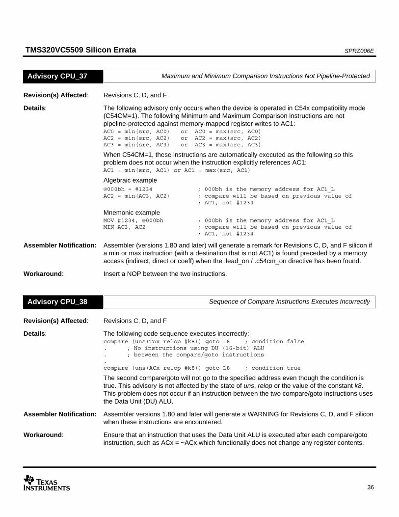
SPRZ006ETMS320VC5509 Silicon Errata
36
Maximum and Minimum Comparison Instructions Not Pipeline-ProtectedAdvisory CPU_37
Revision(s) Affected: Revisions C, D, and F
Details: The following advisory only occurs when the device is operated in C54x compatibility mode(C54CM=1). The following Minimum and Maximum Comparison instructions are notpipeline-protected against memory-mapped register writes to AC1:AC0 = min(src, AC0) or AC0 = max(src, AC0) AC2 = min(src, AC2) or AC2 = max(src, AC2) AC3 = min(src, AC3) or AC3 = max(src, AC3)
When C54CM=1, these instructions are automatically executed as the following so thisproblem does not occur when the instruction explicitly references AC1:AC1 = min(src, AC1) or AC1 = max(src, AC1)
Algebraic example@000bh = #1234 ; 000bh is the memory address for AC1_LAC2 = min(AC3, AC2) ; compare will be based on previous value of
; AC1, not #1234
Mnemonic exampleMOV #1234, @000bh ; 000bh is the memory address for AC1_LMIN AC3, AC2 ; compare will be based on previous value of
; AC1, not #1234
Assembler Notification: Assembler (versions 1.80 and later) will generate a remark for Revisions C, D, and F silicon ifa min or max instruction (with a destination that is not AC1) is found preceded by a memoryaccess (indirect, direct or coeff) when the .lead_on / .c54cm_on directive has been found.
Workaround: Insert a NOP between the two instructions.
Sequence of Compare Instructions Executes IncorrectlyAdvisory CPU_38
Revision(s) Affected: Revisions C, D, and F
Details: The following code sequence executes incorrectly:compare (uns(TAx relop #k8)) goto L8 ; condition false. ; No instructions using DU (16-bit) ALU . ; between the compare/goto instructions.compare (uns(ACx relop #k8)) goto L8 ; condition true
The second compare/goto will not go to the specified address even though the condition istrue. This advisory is not affected by the state of uns, relop or the value of the constant k8.This problem does not occur if an instruction between the two compare/goto instructions usesthe Data Unit (DU) ALU.
Assembler Notification: Assembler versions 1.80 and later will generate a WARNING for Revisions C, D, and F siliconwhen these instructions are encountered.
Workaround: Ensure that an instruction that uses the Data Unit ALU is executed after each compare/gotoinstruction, such as ACx = ~ACx which functionally does not change any register contents.

SPRZ006ETMS320VC5509 Silicon Errata
37
High-Byte Load Corrupted by Write StallAdvisory CPU_39
Revision(s) Affected: Revisions C, D, and F
Details: When a high byte load instruction (see below) is in the READ phase of the pipeline and aprevious memory write instruction is stalled by a slow memory device, the write stall causesthe byte load data to be corrupted and returned as 0x0000.
Algebraic example:
Case 1:*(#0x40000) = k16 ;store to slow external memory causes
;write stallnop ;(or other single-cycle instruction)nop ;(or other single-cycle instruction)AR1 = high_byte(*AR0) ;high byte load instruction
Case 2:*(#0x40000) = k16 ;store to slow external memory causes
;write stallnop ;(or other single-cycle instruction)AR1 = high_byte(*(#0x40000)) ;high byte load instruction from slow
;memory
Assembler Notification: Assembler (versions 1.8 and later) will generate a REMARK for silicon revisions C, D, and F ifa high_byte() read is preceded by a memory write within 3 cycles.
Workaround: Insert at least three NOPs between the instruction that writes to slow memory and the highbyte load instruction to prevent a write from occurring while the high byte load instruction is inthe READ phase of the pipeline.
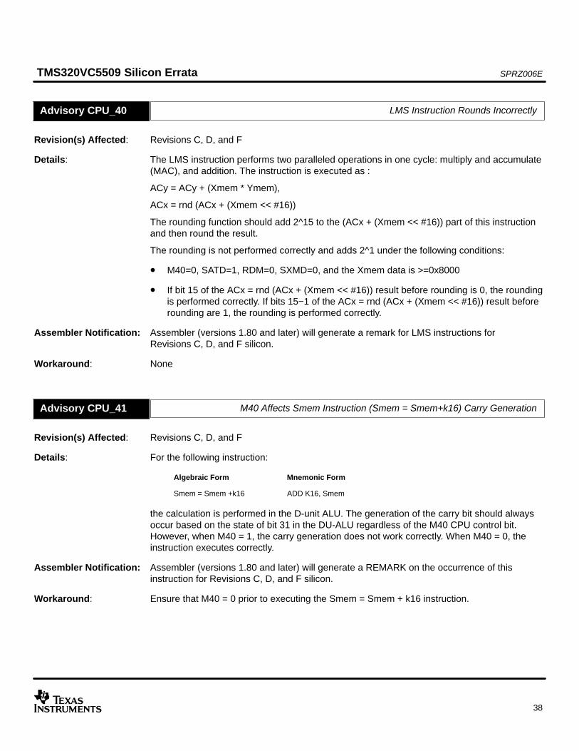
SPRZ006ETMS320VC5509 Silicon Errata
38
LMS Instruction Rounds IncorrectlyAdvisory CPU_40
Revision(s) Affected: Revisions C, D, and F
Details: The LMS instruction performs two paralleled operations in one cycle: multiply and accumulate(MAC), and addition. The instruction is executed as :
ACy = ACy + (Xmem * Ymem),
ACx = rnd (ACx + (Xmem << #16))
The rounding function should add 2^15 to the (ACx + (Xmem << #16)) part of this instructionand then round the result.
The rounding is not performed correctly and adds 2^1 under the following conditions:
• M40=0, SATD=1, RDM=0, SXMD=0, and the Xmem data is >=0x8000
• If bit 15 of the ACx = rnd (ACx + (Xmem << #16)) result before rounding is 0, the roundingis performed correctly. If bits 15−1 of the ACx = rnd (ACx + (Xmem << #16)) result beforerounding are 1, the rounding is performed correctly.
Assembler Notification: Assembler (versions 1.80 and later) will generate a remark for LMS instructions forRevisions C, D, and F silicon.
Workaround: None
M40 Affects Smem Instruction (Smem = Smem+k16) Carry GenerationAdvisory CPU_41
Revision(s) Affected: Revisions C, D, and F
Details: For the following instruction:
Algebraic Form Mnemonic Form
Smem = Smem +k16 ADD K16, Smem
the calculation is performed in the D-unit ALU. The generation of the carry bit should alwaysoccur based on the state of bit 31 in the DU-ALU regardless of the M40 CPU control bit.However, when M40 = 1, the carry generation does not work correctly. When M40 = 0, theinstruction executes correctly.
Assembler Notification: Assembler (versions 1.80 and later) will generate a REMARK on the occurrence of thisinstruction for Revisions C, D, and F silicon.
Workaround: Ensure that M40 = 0 prior to executing the Smem = Smem + k16 instruction.

SPRZ006ETMS320VC5509 Silicon Errata
39
MDP/DP/XSP/SP Updates Not Pipeline-Protected for Extended Register LoadsAdvisory CPU_42
Revision(s) Affected: Revisions C, D, and F
Details:
Case 1: CPL = 0 and MDP/DP
When direct addressing is specified in the Smem field of the auxiliary register load instruction:xdst = mar(Smem)
MDP and DP are read in the address phase of the pipeline. If any previous instruction updatesMDP or DP in the execute or write phases of the pipeline, the updates are notpipeline-protected and the auxiliary register load instruction may not use the updated value.
Case 2: CPL = 1 and XSP/SP
When direct addressing is specified in the Smem field of the auxiliary register load instruction:xdst = mar(Smem)
XSP and SP are read in the address phase of the pipeline. If any previous instruction updatesXSP or SP in the execute or write phases of the pipeline, the updates are notpipeline-protected and the auxiliary register load instruction may not use the updated value.
In both of the above cases, updates to CPL are correctly pipeline-protected.
Case 3: *abs16(#k16) and MDP
When the *abs16(#k16) addressing syntax is specified in the Smem field of the auxiliaryregister load instruction:xdst = mar(Smem)
MDP and DP are read in the address phase of the pipeline. If any previous instruction updatesMDP or DP in the execute or write phases of the pipeline, the updates are notpipeline-protected and the auxiliary register load instruction may not use the updated value.
Algebraic examplebit(ST1, @CPL) = 0 ; clear CPL bitMDP = #0x0 ; MDP updated in the address phaseDP = value1 ; DP updated with value1 in the address phase@DP = value2 ; DP updated with value2 in the execute phasedst = mar(@#0x60) ; auxiliary register load will be based on the
; DP = value1
Assembler Notification: Assembler (versions 1.80 and later) will generate a REMARK on the occurrence of thisinstruction for Revisions C, D, and F silicon.
Workaround: Maintain at least 5 cycles (NOPs or other useful code) between the instruction that modifiesMDP/DP/SP/XSP and the next instruction that uses MDP/DP/SP/XSP with direct or*abs(#k16) addressing.

SPRZ006ETMS320VC5509 Silicon Errata
40
BKxx and BOFxx Updates Not Pipeline-Protected to MAR InstructionAdvisory CPU_43
Revision(s) Affected: Revisions C, D, and F
Details: When any of the following instructions are executed in circular addressing mode, defined byeither ST2 or the circular() qualifier, a BKxx or BOFxx update in the execute or write phaseprior to these instructions is not pipeline-protected.mar(DAy + DAx)mar(DAy − DAx)mar(DAx + P8)mar(DAx − P8)mar(Smem)dst = mar(Smem)
Algebraic example: In the following example, 0x20 should be used as the buffer size but theold value, 0x10 is used.bit(ST2, #0) = 1 ; Set circular addressing mode for AR0....BK03 = #0x10 ; Set circular size for AR0 in ADDRESS phase@BK03 = #0x20 ; Set circular size for AR0 in WRITE phasemar(*AR0+DR0) ; AR0 circular addressing
Assembler Notification: Assembler (versions 1.80 and later) will generate a remark when these instructions occur forRevisions C, D, and F silicon.
Workaround: Maintain at least five cycles (useful code or NOPs) between BKxx & BOFxx updates and marinstructions.
XSP Update Not Pipeline-Protected Against Direct AddressingAdvisory CPU_44
Revision(s) Affected: Revisions C, D, and F
Details: When CPL=1, direct addressing references without the mmap() qualifier are made relative tothe extended stack pointer (XSP:SP). The pipeline should automatically ensure that directaddressing references that follow a stack pointer modification are stalled until the stack pointermodification is completed. The protection of the SP works correctly. However, the protection ofthe XSP does not work correctly.
Algebraic exampleXSSP = old value..XSSP = new value ; XSP is updated in the execute phase*SP(#1) = AR0 ; old value of XSP is read in the address phase
Assembler Notification: Assembler (versions 1.80 and later) will generate a warning for Revisions C, D, and F silicon.
Workaround: Maintain at least four cycles (NOPs or useful code) between the XSP modification and thedirect addressing reference.
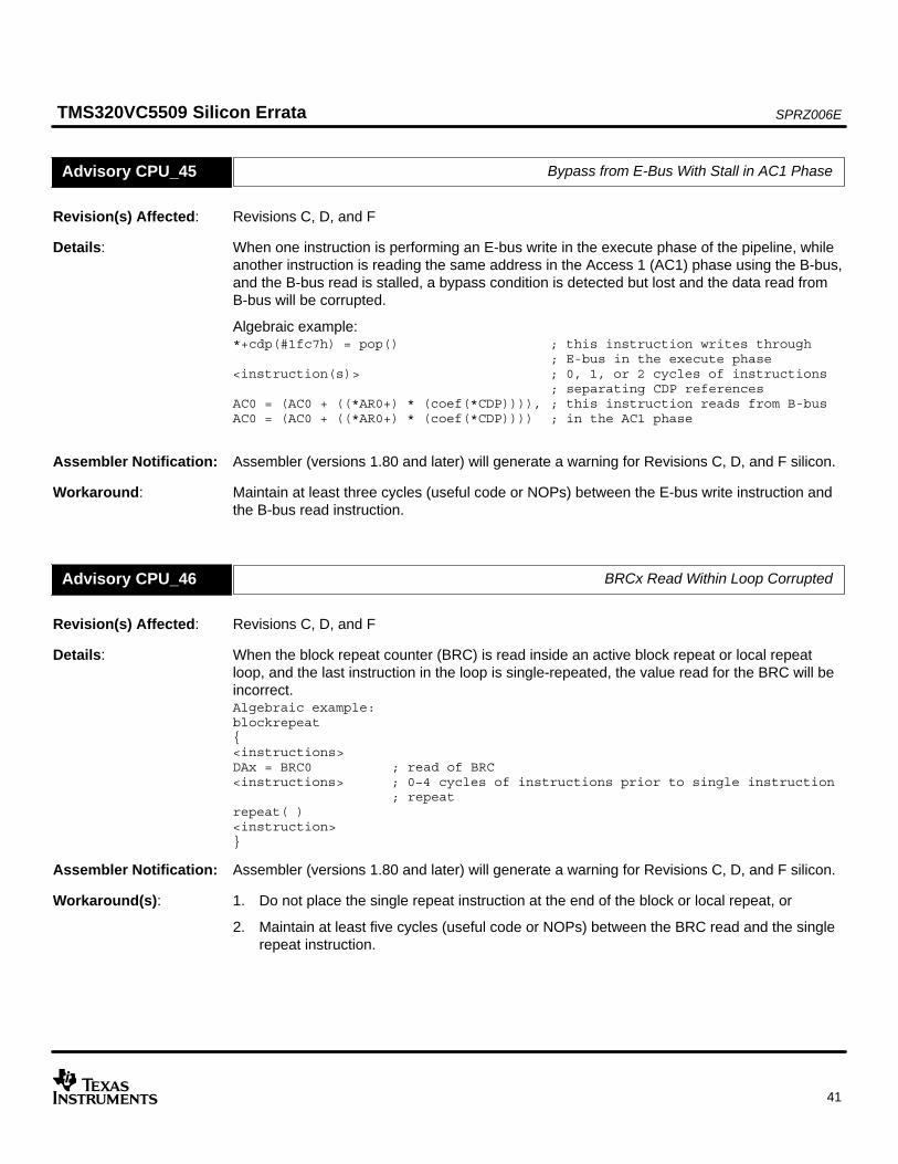
SPRZ006ETMS320VC5509 Silicon Errata
41
Bypass from E-Bus With Stall in AC1 PhaseAdvisory CPU_45
Revision(s) Affected: Revisions C, D, and F
Details: When one instruction is performing an E-bus write in the execute phase of the pipeline, whileanother instruction is reading the same address in the Access 1 (AC1) phase using the B-bus,and the B-bus read is stalled, a bypass condition is detected but lost and the data read fromB-bus will be corrupted.
Algebraic example:*+cdp(#1fc7h) = pop() ; this instruction writes through
; E-bus in the execute phase<instruction(s)> ; 0, 1, or 2 cycles of instructions
; separating CDP referencesAC0 = (AC0 + ((*AR0+) * (coef(*CDP)))), ; this instruction reads from B-busAC0 = (AC0 + ((*AR0+) * (coef(*CDP)))) ; in the AC1 phase
Assembler Notification: Assembler (versions 1.80 and later) will generate a warning for Revisions C, D, and F silicon.
Workaround: Maintain at least three cycles (useful code or NOPs) between the E-bus write instruction andthe B-bus read instruction.
BRCx Read Within Loop CorruptedAdvisory CPU_46
Revision(s) Affected: Revisions C, D, and F
Details: When the block repeat counter (BRC) is read inside an active block repeat or local repeatloop, and the last instruction in the loop is single-repeated, the value read for the BRC will beincorrect.Algebraic example:blockrepeat<instructions>DAx = BRC0 ; read of BRC<instructions> ; 0−4 cycles of instructions prior to single instruction
; repeatrepeat( )<instruction>
Assembler Notification: Assembler (versions 1.80 and later) will generate a warning for Revisions C, D, and F silicon.
Workaround(s): 1. Do not place the single repeat instruction at the end of the block or local repeat, or
2. Maintain at least five cycles (useful code or NOPs) between the BRC read and the singlerepeat instruction.

SPRZ006ETMS320VC5509 Silicon Errata
42
Parallel Execution of Exponent or Normalization InstructionsAdvisory CPU_47
Revision(s) Affected: Revisions C, D, and F
Details: In code execution of the following form:<instruction1> || <exponent/normalization instruction in slot 2>.<non-parallel instruction(s)>.<exponent/normalization instruction> ;this instruction will fail
the second exponent/normalization instruction will fail. The exponent/normalization instructionsinvolved are:
Algebraic Form Mnemonic Form
ACy = mant(ACx), Tx = −exp(ACx) MANT ACx, ACy :: NEXP ACx, Tx
Tx = exp(ACx) EXP ACx, Tx
Assembler Notification: Assembler (versions 1.80 and later) will generate a warning for Revisions C, D, and F silicon.
Workaround: Ensure the second instance of the exponent/normalization instruction is always in parallel withanother instruction (nop or useful code) as in the following example:<instruction1> || Tx = exp(TCx)<non-parallel instruction(s)>Tx = exp(TCx) || nop
Updates of T1 in *(ARx −/+ T1) With Dual Access Not Pipeline-Protected When ARMS = 1Advisory CPU_48
Revision(s) Affected: Revisions C, D, and F
Details: If a parallel instruction pair performs a dual access and uses the addressing mode *(ARx −/+T1), updates of T1 are not pipeline-protected when the updates occur in the write or executephases of the instructions prior to the parallel instruction pair.
This advisory occurs when the instruction using the addressing mode *(ARx −/+ T1) is either inthe first or second position in the parallel instruction pair.
Algebraic examplebit(ST2,#15) = #1 ; ARMS bit = 1..T1 = SSP ; T1 is loaded with SSP in the execute phase.*(AR6+T1) || *AR0 ; AR6 should be incremented by the SSP value but
; uses the previous T1 value instead.
Assembler Notification: Assembler (versions 2.20 and later) will generate a warning for Revisions C, D, and F silicon.
Workaround: Maintain at least five cycles (useful code or NOPs) between the instruction that instruction thatupdates T1 and the instruction pair that uses the *(ARx −/+ T1) indirect addressing mode.
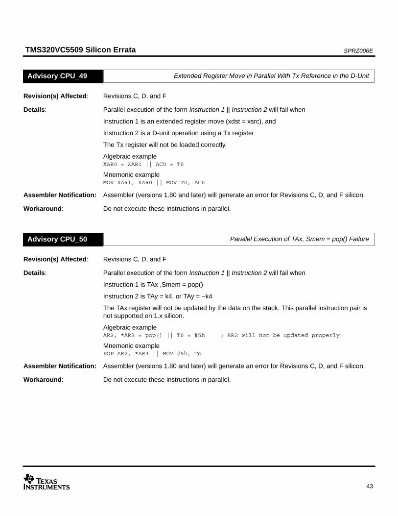
SPRZ006ETMS320VC5509 Silicon Errata
43
Extended Register Move in Parallel With Tx Reference in the D-UnitAdvisory CPU_49
Revision(s) Affected: Revisions C, D, and F
Details: Parallel execution of the form Instruction 1 || Instruction 2 will fail when
Instruction 1 is an extended register move (xdst = xsrc), and
Instruction 2 is a D-unit operation using a Tx register
The Tx register will not be loaded correctly.
Algebraic exampleXAR0 = XAR1 || AC0 = T0
Mnemonic exampleMOV XAR1, XAR0 || MOV T0, AC0
Assembler Notification: Assembler (versions 1.80 and later) will generate an error for Revisions C, D, and F silicon.
Workaround: Do not execute these instructions in parallel.
Parallel Execution of TAx, Smem = pop() FailureAdvisory CPU_50
Revision(s) Affected: Revisions C, D, and F
Details: Parallel execution of the form Instruction 1 || Instruction 2 will fail when
Instruction 1 is TAx ,Smem = pop()
Instruction 2 is TAy = k4, or TAy = −k4
The TAx register will not be updated by the data on the stack. This parallel instruction pair isnot supported on 1.x silicon.
Algebraic exampleAR2, *AR3 = pop() || T0 = #5h ; AR2 will not be updated properly
Mnemonic examplePOP AR2, *AR3 || MOV #5h, To
Assembler Notification: Assembler (versions 1.80 and later) will generate an error for Revisions C, D, and F silicon.
Workaround: Do not execute these instructions in parallel.
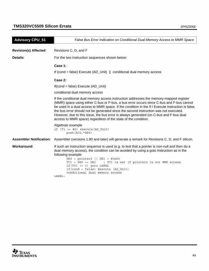
SPRZ006ETMS320VC5509 Silicon Errata
44
False Bus Error Indication on Conditional Dual-Memory Access to MMR SpaceAdvisory CPU_51
Revision(s) Affected: Revisions C, D, and F
Details: For the two instruction sequences shown below:
Case 1:
If (cond = false) Execute (AD_Unit) || conditional dual memory access
Case 2:
if(cond = false) Execute (AD_Unit)
conditional dual memory access
If the conditional dual memory access instruction addresses the memory-mapped register(MMR) space using either C-bus or F-bus, a bus error occurs since C-bus and F-bus cannotbe used in a dual access to MMR space. If the condition in the If / Execute instruction is false,the bus error should not be generated since the second instruction was not executed.However, due to this issue, the bus error is always generated (on C-bus and F-bus dualaccess to MMR space) regardless of the state of the condition.
Algebraic exampleif (T1 >= #0) execute(AD_Unit)
push(AC2,*AR4)
Assembler Notification: Assembler (versions 1.80 and later) will generate a remark for Revisions C, D, and F silicon.
Workaround: If such an instruction sequence is used (e.g. to test that a pointer is non-null and then do adual memory access), the condition can be avoided by using a goto instruction as in thefollowing example:
DR0 = pointer2 || DR1 = #0x60TC1 = DR0 >= DR1 ; TC1 is set if pointer2 is not MMR access.if(TC1 != 1) goto LABEL if(cond = false) Execute (AD_Unit)conditional dual memory access
LABEL:

SPRZ006ETMS320VC5509 Silicon Errata
45
Lmem = pair(TAx) in Parallel With TAx Update in Execute PhaseAdvisory CPU_52
Revision(s) Affected: Revisions C, D, and F
Details: Parallel execution of the form Instruction 1 || Instruction 2 will fail when
Instruction 2 is Lmem = pair(TAx) and
Instruction 1 updates a (TAx+1) register in the execute phase
The (TAx+1) register will not be loaded correctly. This form of parallelism is currently notsupported.
Algebraic exampleAR1 = AC0 − Smem || Smem = pair(AR0) ; AR1 will not be updated
Mnemonic exampleSUB Smem, AC0, AR1 || MOV pair(AR0), dbl(Lmem) ; AR1 will not be updated
Assembler Notification: None
Workaround: Do not execute these instructions in parallel.
ACx, dst2 = pop() in Parallel With ACy = k4/−k4/k16Advisory CPU_53
Revision(s) Affected: Revisions C, D, and F
Details: Parallel execution of the form Instruction 1 || Instruction 2 will fail when
Instruction 1 is ACx, dst2 = pop()
Instruction 2 is ACy = k4 or ACy = −k4 or ACy = k16
and ACx is not the same accumulator as ACy.
The ACx will not be updated by the pop instruction. This sequence fails only when ACx is inthe dst1 position in Instruction1.
Algebraic exampleAC2,T1 = pop() || AC1 = #0 ; AC2 will not be updated correctly
Mnemonic examplePOP AC2, T1 || MOV #0, AC1 ; AC2 will not be updated correctly
Assembler Notification: Assembler (versions 1.80 and later) will generate an error for Revisions C, D, and F silicon.
Workaround: Do not execute these instructions in parallel.

SPRZ006ETMS320VC5509 Silicon Errata
46
DP Update by bit(ST0,#8−0) Followed by XDP Move is Not Pipeline-ProtectedAdvisory CPU_54
Revision(s) Affected: Revisions C, D, and F
Details: If one of the following Status Bit Set/Clear instructions alters the DP field in status register 0(ST0_55):
• bit(ST0,k4) = #0 or ;clear of bit in DP field of ST0_55 (k4 = #8−0)
• bit(ST0,k4) = #1 ;set of bit in DP field of ST0_55 (k4 = #8−0)
and the instruction is directly followed by one of the following move instructions:
• XARx = XDP
• XCDP = XDP
• XSP = XDP
• XSSP = XDP
the extended registers are updated with the previous XDP value (from before the bitmodification) instead of the correct value.
Algebraic exampleDP = #0xffff ;DP value is initially #0xffffbit(ST0, #8) = #0 ;clear of bit 8 in ST0_55XAR0 = XDP ;XAR0 should be updated to
;0x7FFF but is incorrectly ;updated to 0xFFFF
Mnemonic exampleMOV #0xffff, DP ;DP value is initially #0xffffBCLR #8, ST0_55 ;clear of bit 8 in ST0_55MOV XDP, XAR0 ;XAR0 should be updated to
;0x7FFF but is incorrectly ;updated to 0xFFFF
Assembler Notification: Assembler (versions 1.80 and later) will generate a REMARK for Revisions C, D, and F siliconwhen it sees the above situation.
Workaround: Insert a NOP between the bit instruction and the move from XDP.

SPRZ006ETMS320VC5509 Silicon Errata
47
AR0 is Not Pipeline-Protected When Read by coef(*(CDP+T0)) With C54CM = 1Advisory CPU_55
Revision(s) Affected: Revisions C, D, and F
Details: When the C54CM bit in status register 1 (ST1_55) is set to 1, coef(*(CDP+T0)) is computed ascoef(*(CDP+AR0)). If any previous instruction updates the AR0 register during the execute orwrite phases, the pipeline should stall to postpone coef(*(CDP+T0)) but it does not.
Algebraic examplebit(ST1,#5) = #1 ; set C54CM (=1)CDP = #0x0 ; CDP is loaded with 0x0nopnopmar(AR0 = #0xdead) ; AR0 is loaded with 0xdeadAR0 = #0xaaaa ; AR0 is loaded with 0xaaaa*AR5 = coef(*(CDP+T0)) ; CDP is incorrectly loaded with 0xdead
; instead of 0xaaaa
Mnemonic exampleBSET #5, ST1_55 ; set C54CM (=1)MOV #0x0, CDP ; CDP is loaded with 0x0nopnopAMOV #0xdead, AR0 ; AR0 is loaded with 0xdeadMOV #0xaaaa, AR0 ; AR0 is loaded with 0xaaaaMOV coef(*(CDP+T0)), *AR5 ; CDP is incorrectly loaded with 0xdead
; instead of 0xaaaa
NOTE: The syntax for coef(*(CDP+T0)) in both examples may be changed to coef(*(CDP+AR0))when C54CM is set to 1.
Assembler Notification: Whenever the assembler (versions 1.80 and later) sees a write of AR0 or a memory write,followed within five cycles by the coef form above, it will generate a REMARK for Revisions C,D, and F silicon.
Workaround: Maintain at least five cycles (useful code or NOPs) between the instruction that updates AR0and the instruction using coef(*(CDP+T0)).

SPRZ006ETMS320VC5509 Silicon Errata
48
ARMS Bit Incorrectly Affects *(ARn+T1) in Parallel With Another DAGEN InstructionAdvisory CPU_56
Revision(s) Affected: Revisions C, D, and F
Details: In the case of single access memory, when ARMS=1 in status register 2 (ST2_55), *(ARn+T1)is computed as *ARn(short(#1)). In the case of dual access memory, *(ARn+T1) should not beaffected by the ARMS bit and should be computed as it is. However, in this case (dual accessmemory), when two instructions using the data address generation unit (DAGEN) areexecuted in parallel (DAGEN instr1 || DAGEN instr2) with ARMS=1, *(ARn+T1) is incorrectlycomputed as *ARn(short(#1)).
NOTE: Using implied parallelism with two DAGEN instructions (DAGEN instr1, DAGEN instr2) in this case will workproperly.
Algebraic examplebit(ST2,#15) = #1 ; set ARMS bit to 1AC1 = *(AR3+DR1)|| B0F67 = *(AR5 – DR0) ; instr1 is incorrectly
; calculated as ; *ARn(short(#1))
Assembler Notification: Assembler (versions 2.20 and later) will generate a WARNING for Revisions C, D, and Fsilicon.
Workaround: Reset the ARMS bit to 0 before executing two DAGEN instructions in parallel (DAGEN ||DAGEN) using *(ARn+T1) and dual access memory.
TRNx Register Not UpdatedAdvisory CPU_57
Revision(s) Affected: Revisions C, D, and F
Details: In the following cases, both TRN0 and TRN1 registers should be updated by both instructionsof each parallel instruction pair (Instruction1 || Instruction2), but Instruction1 does not updateTRNx.
TRN0 = Smem || max_diff_dbl(ACx,ACy,ACz,ACw,TRN1) ;TRN0 is not updatedTRN1 = Smem || max_diff_dbl(ACx,ACy,ACz,ACw,TRN0) ;TRN1 is not updated TRN0 = Smem || min_diff_dbl(ACx,ACy,ACz,ACw,TRN1) ;TRN0 is not updated TRN1 = Smem || min_diff_dbl(ACx,ACy,ACz,ACw,TRN0) ;TRN1 is not updated
NOTE: If the same TRNx register is selected by both instructions, TRNx is updated by Instruction2. This behavior iscorrect.
Assembler Notification: Assembler (versions 1.80 and later) will generate an ERROR for Revisions C, D, and F siliconwhen these pairs are found.
Workaround: Do not execute these instructions in parallel.
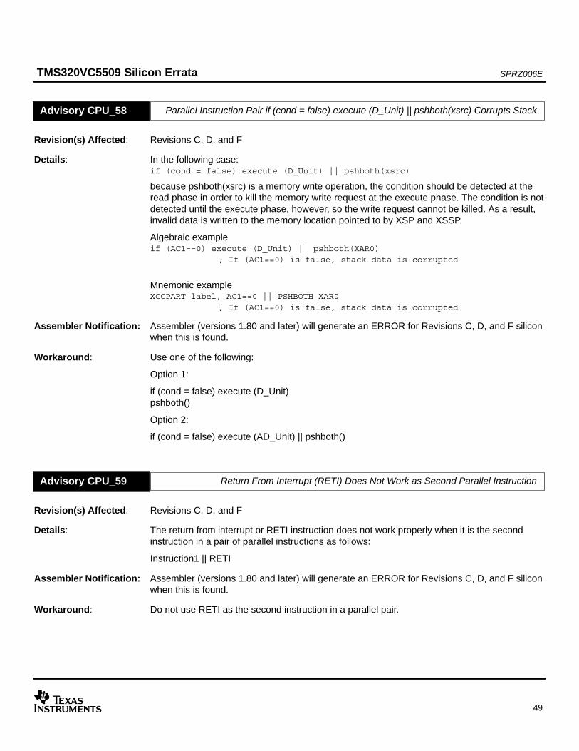
SPRZ006ETMS320VC5509 Silicon Errata
49
Parallel Instruction Pair if (cond = false) execute (D_Unit) || pshboth(xsrc) Corrupts StackAdvisory CPU_58
Revision(s) Affected: Revisions C, D, and F
Details: In the following case:if (cond = false) execute (D_Unit) || pshboth(xsrc)
because pshboth(xsrc) is a memory write operation, the condition should be detected at theread phase in order to kill the memory write request at the execute phase. The condition is notdetected until the execute phase, however, so the write request cannot be killed. As a result,invalid data is written to the memory location pointed to by XSP and XSSP.
Algebraic exampleif (AC1==0) execute (D_Unit) || pshboth(XAR0)
; If (AC1==0) is false, stack data is corrupted
Mnemonic exampleXCCPART label, AC1==0 || PSHBOTH XAR0
; If (AC1==0) is false, stack data is corrupted
Assembler Notification: Assembler (versions 1.80 and later) will generate an ERROR for Revisions C, D, and F siliconwhen this is found.
Workaround: Use one of the following:
Option 1:
if (cond = false) execute (D_Unit)pshboth()
Option 2:
if (cond = false) execute (AD_Unit) || pshboth()
Return From Interrupt (RETI) Does Not Work as Second Parallel InstructionAdvisory CPU_59
Revision(s) Affected: Revisions C, D, and F
Details: The return from interrupt or RETI instruction does not work properly when it is the secondinstruction in a pair of parallel instructions as follows:
Instruction1 || RETI
Assembler Notification: Assembler (versions 1.80 and later) will generate an ERROR for Revisions C, D, and F siliconwhen this is found.
Workaround: Do not use RETI as the second instruction in a parallel pair.
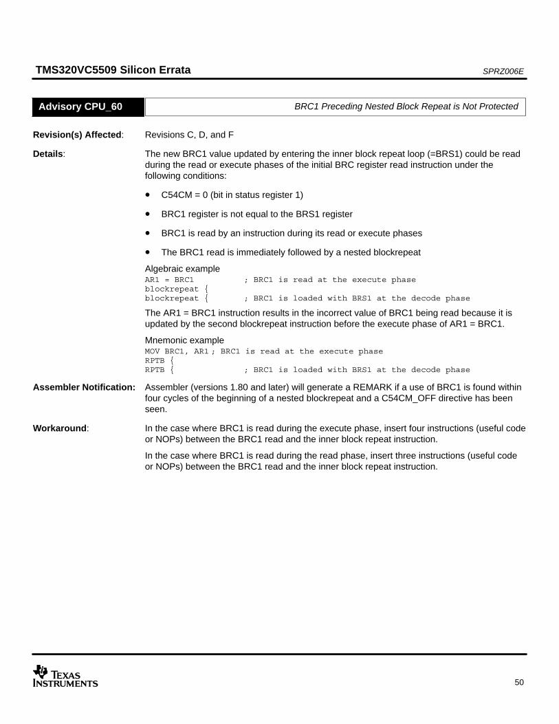
SPRZ006ETMS320VC5509 Silicon Errata
50
BRC1 Preceding Nested Block Repeat is Not ProtectedAdvisory CPU_60
Revision(s) Affected: Revisions C, D, and F
Details: The new BRC1 value updated by entering the inner block repeat loop (=BRS1) could be readduring the read or execute phases of the initial BRC register read instruction under thefollowing conditions:
• C54CM = 0 (bit in status register 1)
• BRC1 register is not equal to the BRS1 register
• BRC1 is read by an instruction during its read or execute phases
• The BRC1 read is immediately followed by a nested blockrepeat
Algebraic exampleAR1 = BRC1 ; BRC1 is read at the execute phaseblockrepeat blockrepeat ; BRC1 is loaded with BRS1 at the decode phase
The AR1 = BRC1 instruction results in the incorrect value of BRC1 being read because it isupdated by the second blockrepeat instruction before the execute phase of AR1 = BRC1.
Mnemonic exampleMOV BRC1, AR1 ; BRC1 is read at the execute phaseRPTB RPTB ; BRC1 is loaded with BRS1 at the decode phase
Assembler Notification: Assembler (versions 1.80 and later) will generate a REMARK if a use of BRC1 is found withinfour cycles of the beginning of a nested blockrepeat and a C54CM_OFF directive has beenseen.
Workaround: In the case where BRC1 is read during the execute phase, insert four instructions (useful codeor NOPs) between the BRC1 read and the inner block repeat instruction.
In the case where BRC1 is read during the read phase, insert three instructions (useful codeor NOPs) between the BRC1 read and the inner block repeat instruction.

SPRZ006ETMS320VC5509 Silicon Errata
51
MAC Operation is Affected by an M40 Qualifier Instruction Executed in ParallelAdvisory CPU_61
Revision(s) Affected: Revisions C, D, and F
Details: When the M40 bit in status register 1 (ST1_55) is 0 and one of the following parallel instructionpairs is executed:
• (instruction with M40 qualifier) || (MAC instruction without M40 qualifier) ; or
• (MAC instruction without M40 qualifier) || (M40 qualifier instruction)
the MAC instruction computes as if M40 is 1, even though it has no M40 qualifier.
Algebraic examplebit(ST1,@M40) = #0AC0 = M40(dbl(@#36h)) || AC3 = (AC3 * T0) + AC3
The MAC instruction in the example above should operate in 32-bit mode, however, theparallel instruction with the M40 qualifier affects the MAC operation.
Mnemonic exampleBCLR @M40, ST1_55MOV40 dbl(@#36h) || MAC AC3, T0, AC3, AC3
Assembler Notification: Assembler (versions 1.80 and later) will generate a REMARK for Revisions C, D, and F siliconwhen this pair is found.
Workaround: Do not execute a MAC instruction and an instruction with an M40 qualifier in parallel.
TAx, Acy = pop() || TAz = k4/–k4 Does Not Update TAxAdvisory CPU_62
Revision(s) Affected: Revisions C, D, and F
Details: When one of the following parallel instruction pairs is executed:TAx, ACy = pop() || dst = k4 ; orTAx, ACy = pop() || dst = −k4the TAx register specified in the pop() instruction is not updated.
Assembler Notification: Assembler (versions 2.00 and later) will generate a ERROR for Revisions C, D, and F siliconwhen this pair is found.
Workaround: Swap the positions of Instruction1 and Instruction2 as follows:dst = k4 || TAx, ACy = pop()
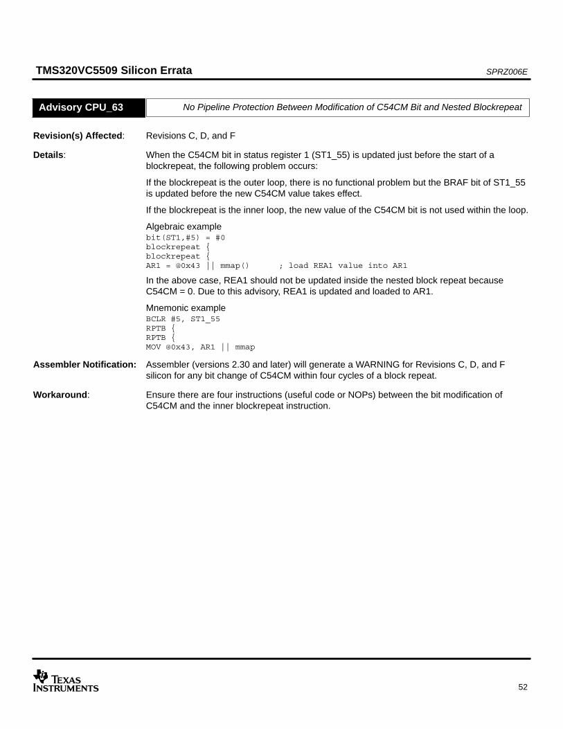
SPRZ006ETMS320VC5509 Silicon Errata
52
No Pipeline Protection Between Modification of C54CM Bit and Nested BlockrepeatAdvisory CPU_63
Revision(s) Affected: Revisions C, D, and F
Details: When the C54CM bit in status register 1 (ST1_55) is updated just before the start of ablockrepeat, the following problem occurs:
If the blockrepeat is the outer loop, there is no functional problem but the BRAF bit of ST1_55is updated before the new C54CM value takes effect.
If the blockrepeat is the inner loop, the new value of the C54CM bit is not used within the loop.
Algebraic examplebit(ST1,#5) = #0blockrepeat blockrepeat AR1 = @0x43 || mmap() ; load REA1 value into AR1
In the above case, REA1 should not be updated inside the nested block repeat becauseC54CM = 0. Due to this advisory, REA1 is updated and loaded to AR1.
Mnemonic exampleBCLR #5, ST1_55RPTB RPTB MOV @0x43, AR1 || mmap
Assembler Notification: Assembler (versions 2.30 and later) will generate a WARNING for Revisions C, D, and Fsilicon for any bit change of C54CM within four cycles of a block repeat.
Workaround: Ensure there are four instructions (useful code or NOPs) between the bit modification ofC54CM and the inner blockrepeat instruction.
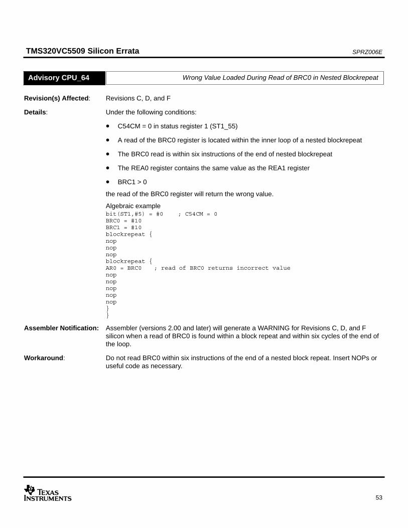
SPRZ006ETMS320VC5509 Silicon Errata
53
Wrong Value Loaded During Read of BRC0 in Nested BlockrepeatAdvisory CPU_64
Revision(s) Affected: Revisions C, D, and F
Details: Under the following conditions:
• C54CM = 0 in status register 1 (ST1_55)
• A read of the BRC0 register is located within the inner loop of a nested blockrepeat
• The BRC0 read is within six instructions of the end of nested blockrepeat
• The REA0 register contains the same value as the REA1 register
• BRC1 > 0
the read of the BRC0 register will return the wrong value.
Algebraic examplebit(ST1,#5) = #0 ; C54CM = 0BRC0 = #10BRC1 = #10blockrepeat nopnopnopblockrepeat AR0 = BRC0 ; read of BRC0 returns incorrect valuenopnopnopnopnop
Assembler Notification: Assembler (versions 2.00 and later) will generate a WARNING for Revisions C, D, and Fsilicon when a read of BRC0 is found within a block repeat and within six cycles of the end ofthe loop.
Workaround: Do not read BRC0 within six instructions of the end of a nested block repeat. Insert NOPs oruseful code as necessary.

SPRZ006ETMS320VC5509 Silicon Errata
54
BRAF Bit is Cleared by return || far() With C54CM=1Advisory CPU_65
Revision(s) Affected: Revisions C, D, and F
Details: When C54CM = 1 in status register 1 (ST1_55), the instruction return || far() should not affectthe BRAF bit. However, the BRAF bit is cleared in this case.
Assembler Notification: Assembler (versions 2.00 and later) will generate a WARNING for Revisions C, D, and Fsilicon when return || far() is found.
Workaround: Save the ST1_55 context to the stack or to an available register before call || far() and restoreit after return || far() as in the following example:bit(ST1,#5) = #1 ;C54CM=1blockrepeat.push(@ST1) ; save contextcall #LABEL || far().@ST1 = pop() ;restore context.LABEL:.return || far()

SPRZ006ETMS320VC5509 Silicon Errata
55
Call and Return Are Not Pipeline-Protected Against C54CM Bit UpdateAdvisory CPU_66
Revision(s) Affected: Revisions C, D, and F
Details: As the behavior of call and return instructions is affected by the C54CM bit, these instructionsshould be protected against C54CM bit updates but they are not.
Algebraic examplebit(ST1,#5) = #0 ; clear C54CM bitnopcall #LABEL ; new C54CM bit value is not used
Mnemonic exampleBCLR #5, ST1_55 ; clear C54CM bitNOPCALL #LABEL ; new C54CM bit value is not used
Assembler Notification: Assembler (versions 2.30 and later) will generate a WARNING for Revisions C, D, and Fsilicon when any of the following are detected:
1) Bit(ST1, #5) = # within three cycles of a call or return
2) A direct write to ST1 within four cycles of a call or return
3) Bit(ST1, #5) = # within six cycles of a far call
4) A direct write to ST1 within seven cycles of a far call
Workaround: Maintain at least three instructions (NOPs or useful code) between a C54CM bit update by bitinstruction and a call or return instruction.
Maintain at least four instructions (NOPs or useful code) between a C54CM bit update by ST1MMR write and a call or return instruction.
In the case of a “call || far” instruction:
Maintain at least six instructions (NOPs or useful code) between a C54CM bit update by bitinstruction the “call || far” instruction.
Maintain at least seven instructions (NOPs or useful code) between a C54CM bit update byST1 MMR write and the “call || far” instruction.
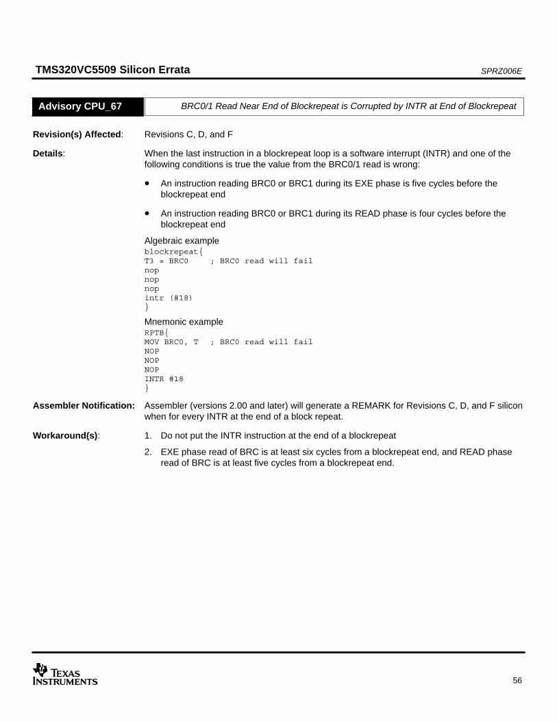
SPRZ006ETMS320VC5509 Silicon Errata
56
BRC0/1 Read Near End of Blockrepeat is Corrupted by INTR at End of BlockrepeatAdvisory CPU_67
Revision(s) Affected: Revisions C, D, and F
Details: When the last instruction in a blockrepeat loop is a software interrupt (INTR) and one of thefollowing conditions is true the value from the BRC0/1 read is wrong:
• An instruction reading BRC0 or BRC1 during its EXE phase is five cycles before theblockrepeat end
• An instruction reading BRC0 or BRC1 during its READ phase is four cycles before theblockrepeat end
Algebraic exampleblockrepeatT3 = BRC0 ; BRC0 read will failnopnopnopintr (#18)
Mnemonic exampleRPTBMOV BRC0, T ; BRC0 read will failNOPNOPNOPINTR #18
Assembler Notification: Assembler (versions 2.00 and later) will generate a REMARK for Revisions C, D, and F siliconwhen for every INTR at the end of a block repeat.
Workaround(s): 1. Do not put the INTR instruction at the end of a blockrepeat
2. EXE phase read of BRC is at least six cycles from a blockrepeat end, and READ phaseread of BRC is at least five cycles from a blockrepeat end.

SPRZ006ETMS320VC5509 Silicon Errata
57
BRAF Access Followed by Interrupt is Not Pipeline-ProtectedAdvisory CPU_68
Revision(s) Affected: Revisions C, D, and F
Details: In the case where an interrupt condition is decoded just after an access to the BRAF bit instatus register 1 (ST1_55), the BRAF access is not pipeline-protected. For example, ifC54CM = 1, an interrupt will cause the BRAF bit to be cleared. A BRAF read preceding theinterrupt could read the cleared BRAF bit instead of the BRAF value present before theinterrupt.
On the Revisions C, D, and F silicon, when C54CM=1, an interrupt condition causes thefollowing to occur:
• Store current BRAF value
• Clear BRAF bit
• Execute ISR
• Restore BRAF value upon return from interrupt
On the a future revision silicon, when C54CM=1, an interrupt will result in the following:
• Store current BRAF value
• Leave BRAF unaltered
• Execute ISR
• Restore BRAF value upon returning from interrupt
Algebraic exampleT3 = @ST1 ; BRAF bit will be cleared before it is stored to T3<interrupt asserted>
Assembler Notification: Assembler (versions 2.30 and later) will generate a REMARK for every direct read of ST1(xxx = @ST1_ L).
Workaround(s): 1. Use the device in native 55x mode.
2. If C54x compatibility mode is enabled, disable the interrupts, read the BRAF bit, and thenenable the interrupts.

SPRZ006ETMS320VC5509 Silicon Errata
58
Conditional D_Unit Execution of MMR Write With False Condition Corrupts MMRAdvisory CPU_69
Revision(s) Affected: Revisions C, D, and F
Details: For the two instruction sequences shown below:
Case 1:If (cond = false) Execute (D_Unit) || MMR write
Case 2:if(cond = false) Execute (D_Unit)MMR write
the memory mapped register (MMR) should not be updated because the condition is false, butin this case the MMR is corrupted. If the condition is true, the MMR is updated correctly.
NOTE: This advisory only occurs with D_Unit.
Algebraic exampleif (AR3 != #0) execute(D_Unit) ;AR3 = 0, condition is false*AR3 = #2 ;MMR at 0x0000h is corrupted
Mnemonic exampleXCCPART label, AR3 != #0 ;AR3 = 0, condition is falseMOV #2, *AR3 ;MMR at 0x0000h is corrupted
Assembler Notification: Assembler (versions 2.30 and later) will generate a WARNING for Revisions C, D, and Fsilicon.
Workaround: Use the AD_Unit instead of the D_Unit in these cases.
Corrupted Read of BRC0/1 Near the End of a BlockrepeatAdvisory CPU_70
Revision(s) Affected: Revisions C, D, and F
Details: When BRC1 or BRC0 is read within seven instructions of the end of blockrepeat loop, the readmay be corrupted under certain pipeline conditions when a stall is being generated.
Assembler Notification: Assembler (versions 2.00 and later) will generate a REMARK for Revisions C, D, and F siliconfor any BRC0/1 read within seven cycles of the end of a block repeat.
Workaround: Do not read BRC0 or BRC1 within seven instructions of the end of a nested blockrepeat.Insert NOPs or useful code as necessary.

SPRZ006ETMS320VC5509 Silicon Errata
59
Potential Pipeline Corruption During InterruptsAdvisory CPU_71
Revision(s) Affected: Revisions C and D
Details: A read on the program bus may be stalled due to a pending memory write. This couldpotentially cause pipeline corruption if an interrupt condition occurs during this time. Thecorruption leads to an illegal value loaded into the Program Counter instead of the ISR startaddress. This condition can occur on double writes to internal memory, single writes to I/Ospace, or a single write to slow external memory through the EMIF. This problem is fixed forinternal memory accesses in silicon Revisions C, D, and F.
This problem can also occur when executing code from external memory (SRAM, SDRAM)that calls a routine in internal memory and an interrupt condition occurs during this time. Thisproblem is corrected in revision F and later devices.
Assembler Notification: None
Workaround: The internal DSP memory is divided into top and bottom sides (TOP and BOT) as shown inthe following example (these are word addresses, not byte addresses):
TOP 0x00000 − 0x07FFFTOP 0x10000 − 0x17FFFTOP 0x20000 − 0x27FFFTOP 0x30000 − 0x37FFF
BOT 0x08000 − 0x0FFFFBOT 0x18000 − 0x1FFFFBOT 0x28000 − 0x2FFFFBOT 0x38000 − 0x3FFFF
The following conditions must be satisfied:
1. While interrupts are active, all internal data accesses must be entirely in the TOP memoryregions or entirely in the BOT memory regions. This includes data and program accessesas well as stack accesses and context stores to the stack. Branches to another side ofmemory are possible only if interrupts are disabled before the branch, and then enabledonce the branch has succeeded.
2. Interrupts must be disabled during all write accesses to external memory and I/O space.
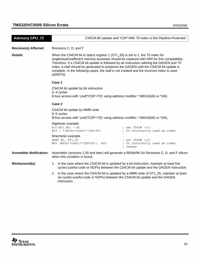
SPRZ006ETMS320VC5509 Silicon Errata
60
C54CM Bit Update and *CDP With T0 Index is Not Pipeline-ProtectedAdvisory CPU_72
Revision(s) Affected: Revisions C, D, and F
Details: When the C54CM bit in status register 1 (ST1_55) is set to 1, the T0 index forsingle/dual/coefficient memory accesses should be replaced with AR0 for 54x compatibility.Therefore, if a C54CM bit update is followed by an instruction utilizing the DAGEN and T0index, a stall should be generated to postpone the DAGEN until the C54CM bit update iscomplete. In the following cases, the stall is not created and the incorrect index is used(AR0/T0):
Case 1
C54CM bit update by bit instruction0−4 cyclesB-bus access with ‘coef(*CDP+T0)’ using address modifier: *ABS16(#k) or *(#k).
Case 2
C54CM bit update by MMR write0−5 cyclesB-bus access with ‘coef(*CDP+T0)’ using address modifier: *ABS16(#k) or *(#k).
Algebraic examplebit(ST1,#5) = #1 ; set C54CM (=1)AC0 = *(#60h)*coef(*(CDP+T0) ; T0 incorrectly used as index
Mnemonic exampleBSET #5, ST1_55 ; set C54CM (=1)MOV (#60h)*coef(*(CDP+T0)), AC0 ; T0 incorrectly used as index
; 0xaaaa
Assembler Notification: Assembler (versions 2.30 and later) will generate a REMARK for Revisions C, D, and F siliconwhen this condition is found.
Workaround(s): 1. In the case where the C54CM bit is updated by a bit instruction, maintain at least fivecycles (useful code or NOPs) between the C54CM bit update and the DAGEN instruction.
2. In the case where the C54CM bit is updated by a MMR write of ST1_55, maintain at leastsix cycles (useful code or NOPs) between the C54CM bit update and the DAGENinstruction.

SPRZ006ETMS320VC5509 Silicon Errata
61
Certain Instructions Not Pipeline-Protected From ResetsAdvisory CPU_73
Revision(s) Affected: Revisions C, D, and F
Details: In the following cases, instructions may not execute properly due to insufficient pipelineprotection from reset conditions:
Case 1
The following instruction(s) is not executed properly when closely preceded by a hardware orsoftware reset:DP = #K16 ;ORDAGEN operation affected by any status bit ;ORif (cond) execute (AD Unit)
These instructions (which depend on ST0_55, ST1_55 and ST2_55) will not execute correctlyif they are located in the first four instructions following the reset (including the delay slot in thereset vector).
Case 2
IFR0/1 or ST1 MMR read instructions may return invalid read data when followed by asoftware reset.
Case 3
The BRAF bit is not cleared correctly by a software reset which follows the bit (ST1, #BRAF) = #1 instruction.
Assembler Notification: None
Workaround: Use the appropriate workaround, based on the Case.
Case 1
Do not put the following instruction(s) in the second slot of a parallel instruction pair. Also donot use the following instruction(s) as the first, second, or third instructions at beginning ofprogram space:DP = #K16 ;ORDAGEN-operation affected by any status bit ;ORif (cond) execute (AD Unit)
Case 2
Ensure at least three cycles between IFR0/1 or ST1 MMR read and a software reset.
Case 3
Ensure at least five cycles between bit(ST1, #BRAF) = #1 and a software reset

SPRZ006ETMS320VC5509 Silicon Errata
62
Tx Not Protected When Paralleled With Extended Register InstructionAdvisory CPU_74
Revision(s) Affected: Revisions C, D, and F
Details: An extra stall should be generated between a Tx update in the EXE phase and its use in theD-Unit. During the following sequence, the stall is not generated and therefore the previousdata of Tx is used by the D-Unit:
1) Tx is updated in EXE phase
2) In the next cycle, instruction slot #1 is one of the following extended register relatedinstructions (instruction does not necessarily have to involve Tx):
dst = srcdst = dbl (Lmem)dbl (Lmem) = srcpshboth (src)dst = popboth()
and instruction slot #2 is a D-unit instruction which uses Tx updated in the previous instruction.
Algebraic exampleT3 = #0.T3 = #1XAR0 = AR3 || AC0 = T3 ;AC0 is updated by #0, not #1
Assembler Notification: Assembler (versions 2.30 and later) will generate a REMARK for Revisions C, D, and F siliconwhen this condition is found.
Workaround: Insert a NOP between the Tx update in EXE phase and the Tx usage by the D-unit in slot #2when paralleled with extended register related instruction in slot #1.
MMR Writes to ST0 and ST2 Are Not Pipeline-Protected Against InterruptsAdvisory CPU_75
Revision(s) Affected: Revisions C, D, and F
Details: Memory mapped writes to the ST0 and ST2 status registers are not Pipeline-Protected againsthardware or software interrupts. The context store of the interrupt should be stalled while thestatus register writes complete, but this is not the case. This will be fixed in silicon a futurerevision.
Algebraic ExampleST0_L = CSR || mmap()<interrupt occurs> ; write to ST0 does not complete
Assembler Notification: Assembler (versions 2.30 and later) will generate a REMARK if an MMR write of ST0/ST1 isdetected.
Workaround(s): 1. In the case of an interrupt caused by the INTR instruction, one NOP should be insertedbetween the MMR ST0/2 register write and the INTR instruction.
2. In the case of hardware interrupts, all interrupts should be masked or disabled until theMMR ST0/2 register write completes. Insert 5 NOPs between the hardware interruptdisable and the MMR ST0/2 write instruction. Insert 6 NOPs between the MMR ST0/2restore and hardware interrupt enable instruction.
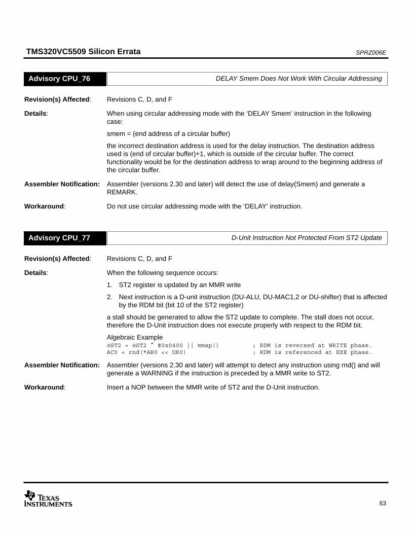
SPRZ006ETMS320VC5509 Silicon Errata
63
DELAY Smem Does Not Work With Circular AddressingAdvisory CPU_76
Revision(s) Affected: Revisions C, D, and F
Details: When using circular addressing mode with the ‘DELAY Smem’ instruction in the followingcase:
smem = (end address of a circular buffer)
the incorrect destination address is used for the delay instruction. The destination addressused is (end of circular buffer)+1, which is outside of the circular buffer. The correctfunctionality would be for the destination address to wrap around to the beginning address ofthe circular buffer.
Assembler Notification: Assembler (versions 2.30 and later) will detect the use of delay(Smem) and generate aREMARK.
Workaround: Do not use circular addressing mode with the ‘DELAY’ instruction.
D-Unit Instruction Not Protected From ST2 UpdateAdvisory CPU_77
Revision(s) Affected: Revisions C, D, and F
Details: When the following sequence occurs:
1. ST2 register is updated by an MMR write
2. Next instruction is a D-unit instruction (DU-ALU, DU-MAC1,2 or DU-shifter) that is affectedby the RDM bit (bit 10 of the ST2 register)
a stall should be generated to allow the ST2 update to complete. The stall does not occur,therefore the D-Unit instruction does not execute properly with respect to the RDM bit.
Algebraic Example@ST2 = @ST2 ^ #0x0400 || mmap() ; RDM is reversed at WRITE phase.AC0 = rnd(*AR0 << DR0) ; RDM is referenced at EXE phase.
Assembler Notification: Assembler (versions 2.30 and later) will attempt to detect any instruction using rnd() and willgenerate a WARNING if the instruction is preceded by a MMR write to ST2.
Workaround: Insert a NOP between the MMR write of ST2 and the D-Unit instruction.

SPRZ006ETMS320VC5509 Silicon Errata
64
Assembler Does Not Detect Violation of Max Local Repeat Block SizeAdvisory CPU_78
Revision(s) Affected: Revisions C, D, and F
Details: The maximum size of a repeat block local to the IBQ was defined in the instruction setreference guides as being limited to 61 bytes. This 61-byte limit is not accurate in allconditions, therefore the documentation is in error. Assemblers 2.00 and earlier check toensure that the size of a local repeat block, excluding the last instruction, is less than or equalto 55 bytes. Under the following conditions:
• The repeat block is misaligned such that it starts at the 4th byte of the IBQ
• The last instruction of the repeat block is seven bytes (3-byte body + *(#k) addressingmode)
The size of the repeat block (minus the last instruction) should actually be limited to 54 bytes.If this limit is exceeded in this case, the loop will not fit within the IBQ, causing the CPU tohang.
Even though this is a specification error and not a hardware exception, it is included in thisdocument to inform the user of this condition and its effect (possible CPU hang).
Assembler Notification: Assembler (versions 2.20 and later) will check for the proper maximum local repeat block sizefor all silicon revisions.
Workaround(s): 1. Ensure that the size of a local repeat block excluding the last instruction is equal to or lessthan 54 bytes. A future version of the assembler will check for the proper limit.
OR
2. If the last instruction of a local repeat block is a 7-byte instruction (3-byte body + *(#k)addressing mode), and the remainder of the local repeat block is 55 bytes, use the ‘.align’directive to align the first instruction of the local repeat block to a 32-bit boundary. This willensure the repeat block is aligned to the first byte of the IBQ.
IDLE Cannot Copy the Content of ICR to ISTRAdvisory CPU_79
Revision(s) Affected: Revisions C, D, and F
Details: When an IDLE instruction is decoded, the content of the Idle Configuration Register (ICR) issupposed to be copied to Idle Status Register (ISTR) when the instruction preceding the IDLEcompletes its WRITE phase. However, during the following sequence, the ICR to ISTR copydoes not happen:
• IDLE is decoded• A wakeup interrupt condition (NMI or any maskable interrupt which is enabled in the
IER0/IER1 registers) is captured or is currently pending.• The ICR to ISTR would normally happen here, but does not occur.
Assembler Notification: None
Workaround: Make sure all interrupts are masked (disabled) via the IER0/IER1 registers before IDLEinstruction is decoded. This workaround does not work for the NMI interrupt.

SPRZ006ETMS320VC5509 Silicon Errata
65
SP/SSP Access Followed by a Conditional Execute is Not Protected Against InterruptsAdvisory CPU_84
Revision(s) Affected: Revisions C, D, and F
Details: Any of the following instructions are not protected against interrupts when followed by aAD-unit conditional execute instruction for which the condition is false. (This exception onlyapplies to conditional execution of the next instruction and not a conditional execute of aparallel instruction):
• SP = SP + K8 (revision 1.x only)• MMR−read access to SP/SSP• dst = XSP/XSSP• dbl(Lmem) = XSP/XSSP• push_both(XSP/XSSP)• XSP/XSSP = pop()• MMR−write access to SP/SSP
Algebraic ExamplenopSP = SP − #1if (TC1) execute (AD_Unit) ; where TC1 = 0, condition is false.<interrupt occurs>AR6 += #1...
Assembler Notification: Assembler (versions 2.30 and later) will attempt to identify a code sequence that may causethe exception and generate a REMARK.
Workaround: Case 1: When SP/SSP is read in the read phase, insert 2 NOPs between the SP/SSPinstruction and the conditional execute instruction.
Case 2: When SP/SSP is read or written in the execute phase, insert three NOPs betweenthe SP/SSP instruction and the conditional execute instruction.
Case 3: When SP/SSP is written in the write phase, insert four NOPs between the SP/SSPinstruction and the conditional execute instruction.
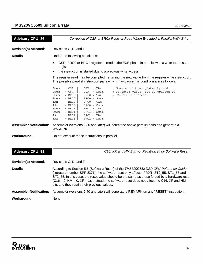
SPRZ006ETMS320VC5509 Silicon Errata
66
Corruption of CSR or BRCx Register Read When Executed in Parallel With WriteAdvisory CPU_86
Revision(s) Affected: Revisions C, D, and F
Details: Under the following conditions:
• CSR, BRC0 or BRC1 register is read in the EXE phase in parallel with a write to the sameregister
• the instruction is stalled due to a previous write access
The register read may be corrupted, returning the new value from the register write instruction.The possible parallel instruction pairs which may cause this condition are as follows:
Smem = CSR || CSR = TAx ; Smem should be updated by oldSmem = CSR || CSR = Smem ; register value, but is updated toSmem = BRC0 || BRC0 = TAx ; TAx value insteadSmem = BRC0 || BRC0 = SmemTAx = BRC0 || BRC0 = TAxTAx = BRC0 || BRC0 = SmemSmem = BRC1 || BRC1 = TAxSmem = BRC1 || BRC1 = SmemTAx = BRC1 || BRC1 = TAxTAx = BRC1 || BRC1 = Smem
Assembler Notification: Assembler (versions 2.30 and later) will detect the above parallel pairs and generate aWARNING.
Workaround: Do not execute these instructions in parallel.
C16, XF, and HM Bits not Reinitialized by Software ResetAdvisory CPU_91
Revision(s) Affected: Revisions C, D, and F
Details: According to Section 5.6 (Software Reset) of the TMS320C55x DSP CPU Reference Guide(literature number SPRU371), the software reset only affects IFR0/1, ST0_55, ST1_55 andST2_55. In this case, the reset value should be the same as those forced by a hardware reset(C16 = 0, HM = 0, XF = 1). Instead, the software reset does not affect the C16, XF and HMbits and they retain their previous values.
Assembler Notification: Assembler (versions 2.40 and later) will generate a REMARK on any “RESET” instruction.
Workaround: None
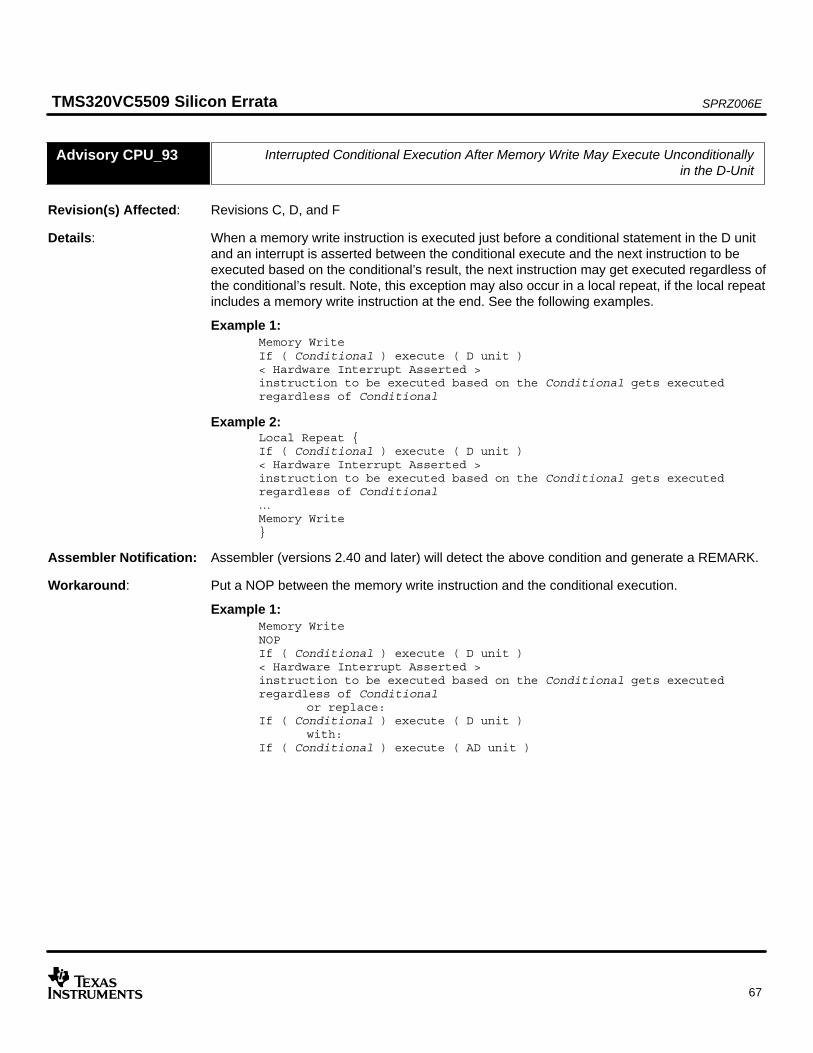
SPRZ006ETMS320VC5509 Silicon Errata
67
Interrupted Conditional Execution After Memory Write May Execute Unconditionallyin the D-Unit
Advisory CPU_93
Revision(s) Affected: Revisions C, D, and F
Details: When a memory write instruction is executed just before a conditional statement in the D unitand an interrupt is asserted between the conditional execute and the next instruction to beexecuted based on the conditional’s result, the next instruction may get executed regardless ofthe conditional’s result. Note, this exception may also occur in a local repeat, if the local repeatincludes a memory write instruction at the end. See the following examples.
Example 1:Memory WriteIf ( Conditional ) execute ( D unit )< Hardware Interrupt Asserted >instruction to be executed based on the Conditional gets executed regardless of Conditional
Example 2:Local Repeat If ( Conditional ) execute ( D unit )< Hardware Interrupt Asserted >instruction to be executed based on the Conditional gets executed regardless of Conditional…Memory Write
Assembler Notification: Assembler (versions 2.40 and later) will detect the above condition and generate a REMARK.
Workaround: Put a NOP between the memory write instruction and the conditional execution.
Example 1:Memory WriteNOPIf ( Conditional ) execute ( D unit )< Hardware Interrupt Asserted >instruction to be executed based on the Conditional gets executed regardless of Conditional
or replace:If ( Conditional ) execute ( D unit )
with:If ( Conditional ) execute ( AD unit )
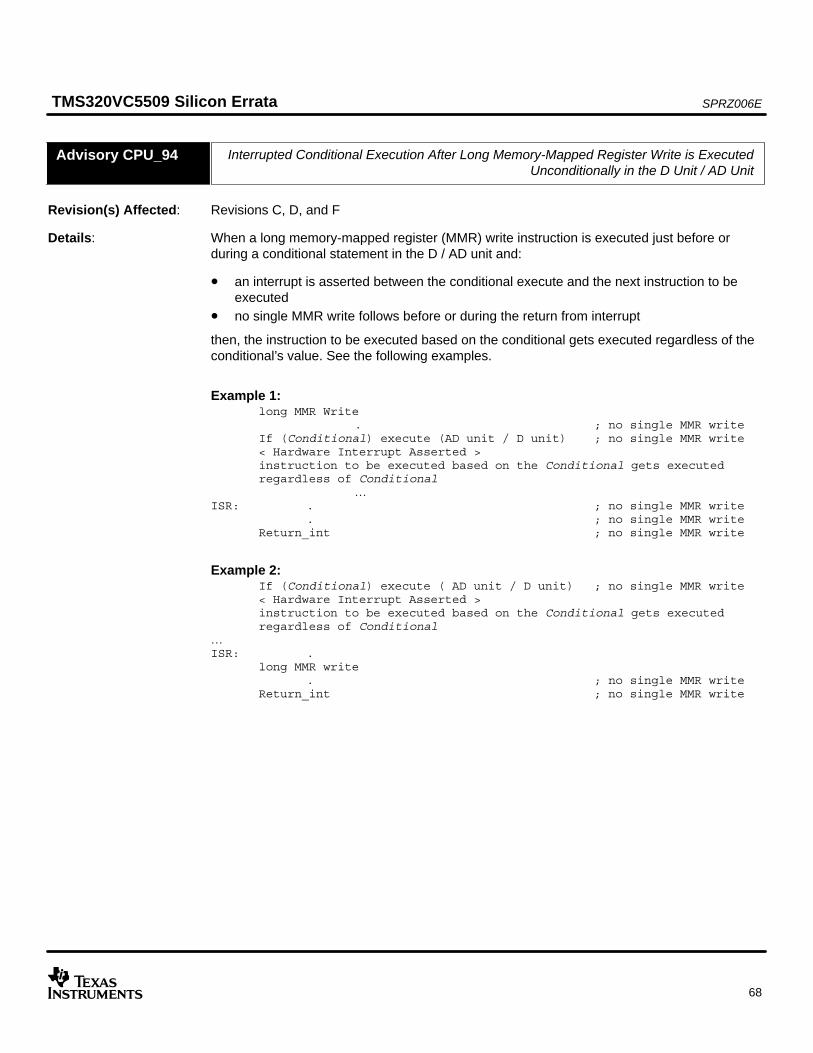
SPRZ006ETMS320VC5509 Silicon Errata
68
Interrupted Conditional Execution After Long Memory-Mapped Register Write is ExecutedUnconditionally in the D Unit / AD Unit
Advisory CPU_94
Revision(s) Affected: Revisions C, D, and F
Details: When a long memory-mapped register (MMR) write instruction is executed just before orduring a conditional statement in the D / AD unit and:
• an interrupt is asserted between the conditional execute and the next instruction to beexecuted
• no single MMR write follows before or during the return from interrupt
then, the instruction to be executed based on the conditional gets executed regardless of theconditional’s value. See the following examples.
Example 1:long MMR Write
. ; no single MMR writeIf (Conditional) execute (AD unit / D unit) ; no single MMR write< Hardware Interrupt Asserted >instruction to be executed based on the Conditional gets executed regardless of Conditional
…ISR: . ; no single MMR write
. ; no single MMR writeReturn_int ; no single MMR write
Example 2:If (Conditional) execute ( AD unit / D unit) ; no single MMR write< Hardware Interrupt Asserted >instruction to be executed based on the Conditional gets executed regardless of Conditional
…ISR: .
long MMR write. ; no single MMR write
Return_int ; no single MMR write

SPRZ006ETMS320VC5509 Silicon Errata
69
Interrupted Conditional Execution After Long Memory-Mapped Register Write is ExecutedUnconditionally in the D Unit / AD Unit (Continued)
Example 3:If ( Conditional ) execute ( AD unit / D unit ) ; no single MMR write< Hardware Interrupt Asserted >instruction to be executed based on the Conditional gets executed regardless of Conditional
…ISR: .
long MMR write || Return_int
long memory mapped register (MMR) is any of the following instructions that point to 0x0through 0x5F with “Lmem” addressing:
dbl( Lmem ) = pop ()dbl( Lmem ) = ACx, copr()dbl( Lmem ) = LCRPCdbl( Lmem ) = srcdbl( Lmem ) = ACxdbl( Lmem ) = saturate( uns( ACx ) )Lmem = pair( Dax )HI( Lmem ) = HI( ACx ) >> #1 , LO( Lmem ) = LO( ACx ) >> #1Lmem = pair( HI( ACx ))Lmem = pair( LO( ACx ))Lmem = dbl( coeff )
Assembler Notification: Assembler (versions 2.40 and later) will generate a REMARK on any return-from-interruptinstruction. The assembler will avoid the remark if it is able to determine that a single memorywrite occurs before the return-from-interrupt and there is no long MMR write between thesingle memory write and the return-from-interrupt instruction.
Workaround: Put a dummy single memory write (e.g. @#0x1f = AR0 || mmap() : 0x1f is a reserved space.)in front of all ”Return_int” and make sure that no long memory writes are in parallel with”Return_int”.
Example 1:long MMR Write
. ; no single MMR writeIf (Conditional) execute (AD unit / D unit) ; no single MMR write< Hardware Interrupt Asserted >instruction not to be executed
…ISR: . ; no single MMR write
. ; no single MMR writesingle MMR writeReturn_int ; no single MMR write

SPRZ006ETMS320VC5509 Silicon Errata
70
“LCRPC = Lmem || Lmem = LCPRC” May Not Work CorrectlyAdvisory CPU_97
Revision(s) Affected: Revisions C, D, and F
Details: “LCRPC = Lmem || Lmem = LCPRC” can be used to update the LCPRC by the data at“Lmem” and save the current LCPRC to the same location as follows:
New LCRPC <− Old Lmem
New LCRPC −> New Lmem
Example 1:
Before execution: LCPRC = 0x00123456, Lmem = 0xFFFFFFFF
After execution: LCRPC = 0xFFFFFFFF, Lmem = 0xFFFFFFFF instead of the expected0x00123456
Assembler Notification: Assembler (versions 2.40 and later) will generate a WARNING if the above condition is found.
Workaround: Do not use the parallel combination of instructions.

SPRZ006ETMS320VC5509 Silicon Errata
71
“return-int” (Under Fast - Ret Config) May Lead to Some InstructionsNot Working Correctly
Advisory CPU_99
Revision(s) Affected: Revisions C, D, and F
Details: Under fast return configuration, when an interrupt is asserted at any of the following cases:
• during single repeat• just before conditional execute next instruction, such as, XCN_PMC, XCN_PMU,
XCN_PMC_S, XCN_PMU_S, etc.
and also if the corresponding ”return_int” is stalled at ADDRESS or ACCESS1 phase,
• the single repeat is executed more than expected and if it is located at the end ofblockrepeat/localrepeat, the BRCx may be not decremented.
• the instruction to be executed conditionally is executed unconditionally.
Example 1:AR0 = #0repeat( #15 )AR0 = AR0 + #1 ; An interrupt is asserted here.AR0 = AR0 ^ #16 ; AR0 is expected to be 0 but not.If ( AR0 != #0 ) goto ERROR …
ISR: .AR1 = AR1 − #1mar( *AR1+ ) || return_int ; Stalled at ADDRESS phase.
Example 2:.<< An interrupt is asserted here >>if ( cond=false ) Execute ( AD_Unit / D_Unit )Instruction to be executed conditionally is executed always.
…ISR: .
AR1 = AR1 − #1mar( *AR1+ ) || return_int ; Stalled at ADDRESS phase.
Assembler Notification: The assembler (versions 2.40 and later) will generate a REMARK on any return-from-interruptinstruction that does not have at least six NOP instructions preceding it.
Workaround: If ”hold” feature, which can cause CPU stall, is not used, put six NOPs just before return_int toavoid it from stall.
Example:.nopnopnopnopnopnopreturn_int ; no stall at ADDRESS nor ACCESS1 phase.
ORNot to use Fast return configuration.

SPRZ006ETMS320VC5509 Silicon Errata
72
Long (32-Bit) Read From MMR Gets CorruptedAdvisory CPU_108
Revision(s) Affected: Revisions C, D, and F
Details: When “Lmem” (see instruction list below) points to address “0x4A” or “0x4D”, twomemory-mapped registers (MMR)—IVPH and ST2 for “0x4A”; SP and SSP for “0x4D”—aresupposed to be read. However, a corrupted value is read from ST2 (for the case of “0x4A”)and SSP (for the case of “0x4D”).
NOTE: The following shows the corresponding part of the MMR mapping.
Address Register
4A IVPH
4B ST2
4C SSP
4D SP
Example
@#0x4a = #0xaaaa || mmap() ; IVPH <= 0xaaaa@#0x4b = #0x1111 || mmap() ; ST2 <= 0x1111push(dbl(@#0x4a)) || mmap() ; @SP−1 <= ST2, @SP−2 <= IVPH
The stack, pointed by SP−1, should be updated with ST2, but instead, gets a corrupted value.
The following is the entire list of Lmem instructions:
• push(dbl(Lmem))
• dbl(coeff) = Lmem
• ACy = ACx + dbl(Lmem)
• ACy = ACx − dbl(Lmem)
• ACy = dbl(Lmem) − ACx
• RETA = dbl(Lmem)
• ACx = M40(dbl(Lmem))
• pair(HI(ACx)) = Lmem
• pair(LO(ACx)) = Lmem
• pair(TAx) = Lmem
• dst = dbl(Lmem)
• HI(ACy) = HI(Lmem) + HI(ACx) , LO(ACy) = LO(Lmem) + LO(ACx)
• HI(ACy) = HI(ACx) − HI(Lmem) , LO(ACy) = LO(ACx) − LO(Lmem)

SPRZ006ETMS320VC5509 Silicon Errata
73
Long (32-Bit) Read From MMR Gets Corrupted (Continued)
• HI(ACy) = HI(Lmem) − HI(ACx) , LO(ACy) = LO(Lmem) − LO(ACx)
• HI(ACx) = Tx − HI(Lmem) , LO(ACx) = Tx − LO(Lmem)
• HI(ACx) = HI(Lmem) + Tx , LO(ACx) = LO(Lmem) + Tx
• HI(ACx) = HI(Lmem) − Tx , LO(ACx) = LO(Lmem) − Tx
• HI(ACx) = HI(Lmem) + Tx , LO(ACx) = LO(Lmem) − Tx
• HI(ACx) = HI(Lmem) − Tx , LO(ACx) = LO(Lmem) + Tx
Assembler Notification: Pending
Workaround: Use “4B” instead of “4A”, “4C” instead of “4D”. For example,@#0x4a = #0xaaaa || mmap() ; IVPH <= 0xaaaa@#0x4b = #0x1111 || mmap() ; ST2 <= 0x1111push(dbl(@#0x4b)) || mmap() ; @SP−1 <= IVPH, @SP−2 <= ST2
Bus Error Issued on Byte Access to I/O Space With Address Range 0x0 to 0x5fAdvisory CPU_109
Revision(s) Affected: Revisions C, D, and F
Details: A bus error, which is captured on IFR1 bit 8 as “BERRINTF” and ST3 bit 7 as “CBERR”, isissued when an illegal bus access occurs. All I/O space (0x0 to 0xffff) is byteread/write-accessible without any bus errors. However, a bus error is wrongly issued when abyte access is made to the I/O space with address range 0x0 to 0x5f.
The following is the entire list of byte-accessible instructions that will give bus errors whentrying to read I/O space address 0x0 to 0x5f:
• dst = uns(high_byte(Smem))
• dst = uns(low_byte(Smem))
• ACx = low_byte(Smem) << SHIFTW
• ACx = high_byte(Smem) << SHIFTW
• high_byte(Smem) = src
• low_byte(Smem) = src
Assembler Notification: Pending
Workaround: Use one of the following workarounds:
• Do not use any of the above instructions to access the I/O space, address 0x0 to 0x5f
• Ignore the bus error, by either not setting IER1[8] or by not using ST3[7].

SPRZ006ETMS320VC5509 Silicon Errata
74
3.3 Device-Level Advisories
Writes to Peripheral Registers Not Pipeline-ProtectedAdvisory DL_1
Revision(s) Affected: Revisions C, D, and F
Details: Writes performed to the peripheral registers (in I/O space) are posted to the peripheralcontroller to be completed in the next available time slot. When the write is posted, theperipheral controller sends a ready signal back to the CPU even though the write has onlybeen posted, not completed. In this case, the CPU has no visibility to any latency associatedwith the write. Since only one write can be posted to the peripheral controller, this effect onlyoccurs on the last write in a sequence because the CPU is stalled if there is more than onewrite request pending to the peripheral controller).
An example of the effect of this exception is configuration writes to the EMIF control registers.The CPU could proceed with a write to external memory space before the final EMIF controlregister write is complete.
Assembler Notification: None
Workaround: The last write in a sequence of writes to peripheral registers can be verified by polling theperipheral register to verify that it has been updated.
Software Modification of MPNMC Bit is Not Pipeline-ProtectedAdvisory DL_2
Revision(s) Affected: Revisions C, D, and F
Details: Software modification of the MPNMC bit in status register 3 (ST3_55) is not pipeline-protectedso changes to the device memory map may not become valid before the instructions thatimmediately follow the modification.
Assembler Notification: None
Workaround: Insert six NOPs after the MPNMC modification.
CLKOUT Output Cannot be Disabled Through ST3_55 RegisterAdvisory DL_3
Revision(s) Affected: Revisions C, D, and F
Details: Setting the CLKOFF bit (CLKOFF = 1) in the ST3_55 register does not cause the CLKOUToutput signal to be disabled.
Assembler Notification: None
Workaround: CLKOUT can be disabled by setting bit 15 (CLKOUT disable) in the External Bus SelectionRegister (0x6C00).

SPRZ006ETMS320VC5509 Silicon Errata
75
Die ID Register Requires TCK (JTAG) Held High to be Read CorrectlyAdvisory DL_6
Revision(s) Affected: Revisions C, D, and F
Details: Reading the Die ID register will give incorrect results if the TCK (JTAG) pin is not held high.
Assembler Notification: None
Workaround: Make sure the TCK pin is not held low during the Die ID Register read operation.
RETI Instruction may Affect the XF StateAdvisory DL_7
Revision(s) Affected: Revisions C, D, and F
Details: The XF pin state is saved on the stack as a part of the ST1 context saving during interruptsservicing. If the XF pin state is changed inside the ISR, upon execution of the RETI, the XF bitwill be restored to the value prior to entering the ISR. If XF state is not changed inside the ISR,then there is no issue.
Assembler Notification: None
Workaround: BIOS takes care of this problem with software workaround, which is transparent to the users.Non-BIOS users who are changing XF pin state in an ISR should also modify the ST1 valueon the stack to maintain the correct XF pin state upon exiting the ISR.
USB and DMA Do Not IDLEAdvisory DL_9
Revision(s) Affected: Revisions C, D, and F
Details: USB and DMA transfer do not IDLE after going through the peripheral IDLE configuration asshown below:
1. Set USB idle (IDLEEN bit) in the USBIDLECTL register
2. Set the PERI bit in the ICR register
3. After the IDLE instruction, USB does not idle
4. Set the DMA IDLE in the ICR register
5. Set the PERI bit in the ICR register
6. After the IDLE instruction, DMA does not idle
Assembler Notification: None
Workaround: None

SPRZ006ETMS320VC5509 Silicon Errata
76
First Word of Data on Consecutive DMA Transmissions Using McBSP is LostAdvisory DL_10
Revision(s) Affected: Revisions C, D, and F
Details: When executing multiple DMA transfers consecutively using the same DMA Transmit Channeland McBSP, an extra DMA TX request generated by the McBSP at the end of the first transferwill not be serviced by the DMA until the next DMA transfer is initiated by the McBSP. At thenext DMA transfer, this DMA TX request will be serviced as soon as the DMA TX channel isenabled.
This transmitted data will remain valid on the bus as long as the McBSP is disabled. However,once the McBSP is enabled, it sends out another DMA TX request, and the DMA transmits thesecond word. This results in the loss of the first word of data on consecutive DMAtransmissions.
Assembler Notification: None
Workaround: Only the systems where McBSP is turned off following each block of DMA transfer areaffected. In such case, a dummy DMA transfer with the DMA synchronization event set to nosync event will flush out the pending TX request from the McBSP before programming theDMA to send the next block of data to the McBSP.
If Bit 2 of Idle Control Register is Not Set, Device Fails to Enter Maximum Idle StateAdvisory DL_11
Revision(s) Affected: Revisions C, D, and F
Details: The device is unable to enter maximum idle state if Bit 2 (Reserved) of the Idle ControlRegister is not set. [Maximum idle state is the state when all clock domains (CPU, peripheral,etc.) that are capable of being idled are idled.]
Assembler Notification: None
Workaround: Always set Bit 2 of the Idle Control Register to enter maximum idle state.
Rev ID Register Shows Incorrect Silicon Revision NumberAdvisory DL_12
Revision(s) Affected: Revision F
Details: Revision F silicon incorrectly identifies itself as silicon revision C or D. Also, the ROMIDregister has the same silicon revision as D.
Assembler Notification: None
Workaround: None
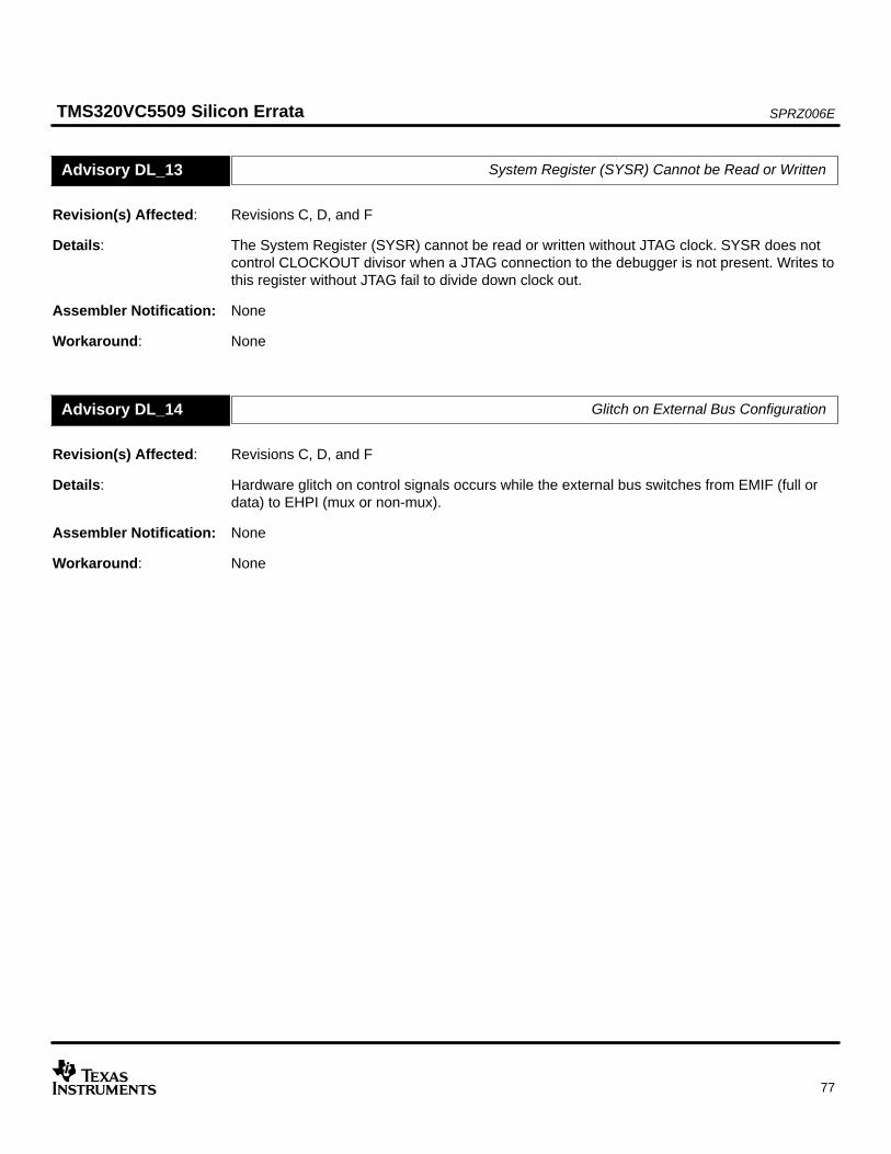
SPRZ006ETMS320VC5509 Silicon Errata
77
System Register (SYSR) Cannot be Read or WrittenAdvisory DL_13
Revision(s) Affected: Revisions C, D, and F
Details: The System Register (SYSR) cannot be read or written without JTAG clock. SYSR does notcontrol CLOCKOUT divisor when a JTAG connection to the debugger is not present. Writes tothis register without JTAG fail to divide down clock out.
Assembler Notification: None
Workaround: None
Glitch on External Bus ConfigurationAdvisory DL_14
Revision(s) Affected: Revisions C, D, and F
Details: Hardware glitch on control signals occurs while the external bus switches from EMIF (full ordata) to EHPI (mux or non-mux).
Assembler Notification: None
Workaround: None
SPRZ006ETMS320VC5509 Silicon Errata
78
Heavy CPU Activity on USB Registers May Stall DMA Channels ServicingOther Peripherals
Advisory DL_15
Revision(s) Affected: Revisions C, D, and F
Details: Heavy CPU activity on the USB registers may stall DMA channels servicing other peripherals(such as McBSPs or GPIOs). The CPU and the DMA share the same peripheral bus to accessthe USB and the McBSP registers. The CPU has the higher priority when there is aresource-sharing conflict between the CPU and the DMA. The USB module operates at24 MHz and takes 6 to 10 cycles (of 24-MHz clock) to complete a CPU read or write request.For a DSP running at 144 MHz, this USB register access time amounts to 36 to 60 cycles ofthe CPU clock and the DMA channel is stalled for this period until the CPU read or write iscomplete.
During the USB module initialization, control data transfer, or interrupt servicing, the CPU mayaccess multiple USB registers back-to-back, which can add up the peripheral bus stall time tothe point where the DMA may start losing McBSP data. This limitation will not affect theperformance of an application during the USB bulk, interrupt, or isochronous data transfersince all USB data endpoints are serviced by the dedicated DMA channels.
Assembler Notification: None
Workaround: Insert NOPs between two register accesses. The number of NOPs to insert depends on theCPU speed. For a DSP running at 144 MHz, one should insert 60 NOPs in between twoback-to-back USB register accesses by the CPU.
The problem is fixed on TMS320VC5509A.

SPRZ006ETMS320VC5509 Silicon Errata
79
3.4 Bootloader Advisories
Boot Mode Selection FailsAdvisory BL_1
Revision(s) Affected: Revision C
Details: The bootloader program included in the on-chip ROM has a problem related to bootmodeselection. This prevents the use of all bootmodes except HPI boot.
Assembler Notification: None
Workaround: This problem only affects customers creating stand-alone demos with the 5509 prototypes.Application code must be reloaded via the HPI or Code Composer Studio IntegratedDevelopment Environment (IDE) each time the system is powered up. This problem iscorrected in Revision D and later of the silicon.
USB Bootloader Returns Incorrect DescriptorType Value When String Descriptors areRequested by the Host
Advisory BL_3
Revision(s) Affected: Revisions D and F
Details: When the host requests for the string descriptor, the USB bootloader returns 0x00 forDescriptorType value instead of 0x03.
Assembler Notification: None
Workaround: Ignore the DescriptorType returned by the DSP. String Descriptor is not necessary forsuccessfully bootloading the device through the USB.
Code Composer Studio is a trademark of Texas Instruments.

SPRZ006ETMS320VC5509 Silicon Errata
80
3.5 Direct Memory Access (DMA) Advisories
Early Sync Event Stops Block TransferAdvisory DMA_1
Revision(s) Affected: Revisions C, D, and F
Details: When a DMA block transfer is initiated by a sync event, if the same sync event occurs beforethe last element of the block transfer has been completed, an event drop occurs and thechannel becomes disabled.
Assembler Notification: None
Workaround: Ensure that the duration between the sync events is long enough to allow the block transfer tocomplete. The DMA end-of-block interrupt can be used as an indicator.
DMA Does Not Support Burst Transfers From EMIF to EMIFAdvisory DMA_2
Revision(s) Affected: Revisions C, D, and F
Details: The DMA controller does not support burst mode transfers with the EMIF as both the sourceand the destination port.
Assembler Notification: None
Workaround: Do not use burst mode for EMIF-to-EMIF transfers.
SYNC Bit Not Held Active for the Entire DMA TransferAdvisory DMA_3
Revision(s) Affected: Revisions C, D, and F
Details: SYNC (synchronization status) bit in the CSR is not held active for the entire duration of theDMA transfer. The bit is only active for the length of the internal DMA request. This preventspolling this bit to determine if a channel is busy.
Assembler Notification: None
Workaround: None

SPRZ006ETMS320VC5509 Silicon Errata
81
DMA Half-Frame Interrupt Occurs at Element (N/2+1) Instead of (N/2)Advisory DMA_4
Revision(s) Affected: Revisions C, D, and F
Details: If data packing is disabled, the DMA half-frame interrupt occurs at element (N/2+1) insteadof N/2. If data packing is enabled, the half-frame interrupt occurs at ≥ N/2.
Assembler Notification: None
Workaround: None
DMA Peripheral Does Not Idle When DMAI Bit Field is Set inIDLEC Configuration Register
Advisory DMA_5
Revision(s) Affected: Revisions C, D, and F
Details: The DMA peripheral does not idle after setting the DMAI bit field and the PERI bit field in theIdle Configuration Register and then executing the IDLE instruction. However, idling the clockdomain will idle the DMA as well.
Assembler Notification: None
Workaround: None

SPRZ006ETMS320VC5509 Silicon Errata
82
3.6 External Memory Interface (EMIF) Advisories
Asynchronous Interface May Fail When HOLD = 0 and ARDY Input is UsedAdvisory EMIF_3
Revision(s) Affected: Revisions C, D, and F
Details: When performing asynchronous memory transfers using ARDY to insert wait-states and withthe READ_HOLD and/or WRITE_HOLD values programmed to 0, subsequent cycles may beprocessed too early causing cycles to fail. This will be corrected in a future revision.
Assembler Notification: None
Workaround: When using the ARDY input with asynchronous memory, program the READ_HOLD andWRITE_HOLD bits of the corresponding CE Space Control Register to 1, 2, or 3.
Setup Period Can be Reduced by One Cycle Under Certain ConditionsAdvisory EMIF_7
Revision(s) Affected: Revisions C, D, and F
Details: During the second and subsequent back-to-back accesses, if the HOLD bit field is set to 0 andthe STROBE bit field is less than or equal to 3 in the CE Space Control Register, then thesetup period is reduced by 1 clock cycle. This does not apply to the first of severalback-to-back accesses nor to isolated accesses.
Assembler Notification: None
Workaround: None
ARDY Pin Requires Strong Pullup ResistorAdvisory EMIF_8
Revision(s) Affected: Revisions C, D, and F
Details: When the parallel bus is used to access external memory, a strong pullup resistor is requiredfor the ARDY pin for the asynchronous memory interface.
Assembler Notification: None
Workaround: Pull up ARDY with a 2.2-kΩ resistor.
SPRZ006ETMS320VC5509 Silicon Errata
83
External Memory Write After Read ReversalAdvisory EMIF_9
Revision(s) Affected: Revisions C, D, and F
Details: If an external memory write is followed immediately by an external memory read, the externalmemory read will occur first, followed by the write. See the example below.
Example:MOV #1770h, *(100001h) ; External Memory WriteMOV *(#100000h), AR1 ; External Memory Read
Assembler Notification: None
Workaround: Insert two NOPs between the memory write/read pair.
Example:MOV #1770h, *(100001h) ; External Memory WriteNOPNOPMOV *(#100000h), AR1 ; External Memory Read
Block Write Immediately Following a Block Read May Cause Data CorruptionAdvisory EMIF_10
Revision(s) Affected: Revisions C, D, and F
Details: When performing a block write immediately following a block read, data may get corrupted.See the example below.
Example:Write 0x55 to addr1Write 0xAA to addr2Read addr1Read addr2
When executed, the above code will follow this order:Write 0x55 to addr1Read addr1Write 0xAA to addr2Read addr2
Assembler Notification: None
Workaround: Insert two NOPs between write and read. Since reads occur before writes in the pipeline, theread must be delayed after the write so that the read does not occur before the write.

SPRZ006ETMS320VC5509 Silicon Errata
84
EMIF Asynchronous Access Hold = 0 is Not Valid for Strobe > 3Advisory EMIF_11
Revision(s) Affected: Revisions C, D, and F
Details: For asynchronous EMIF accesses, a hold time of 0 is not valid for strobe lengths greater than3 cycles if the ARDY_OFF bit is not set. If the above configuration is used but the ARDY_OFFbit is clear, then the EMIF automatically gives a hold time of 1 cycle.
Assembler Notification: None
Workaround: None
8-Bit Asynchronous Mode on 5509 EMIF Not SupportedAdvisory EMIF_12
Revision(s) Affected: Revisions C, D, and F
Details: Access to external memory configured as 8-bit asynchronous memory will no longer besupported.
Assembler Notification: None
Workaround: None
SPRZ006ETMS320VC5509 Silicon Errata
85
After Changing CE Control Registers and Disabling SDRAM Clock in Divide-by-8 andDivide-by-16 Modes, Asynchronous Access Followed by SDRAM Access Will Not Supply
a Ready Signal to CPU
Advisory EMIF_13
Revision(s) Affected: Revisions C, D, and F
Details: If the SDRAM clock (EMIF.CLKMEM) is set to divide-by-8 and divide-by-16 of the CPU clockand if the user disables the SDRAM clock before accessing asynchronous memory, the EMIFwill fail to supply the ready signal to the CPU under the following two conditions:
• Case 1:SDRAM accessSwitch off the SDRAM clockChange CE Space Control Register to Asynchronous ModePerform an asynchronous access to the same CE space
• Case 2:SDRAM accessSwitch off the SDRAM clockChange CE Space Control Register to Asynchronous ModePerform an asynchronous access to a different CE space
This failure of the ready signal will make the CPU wait indefinitely.
Assembler Notification: None
Workaround: Switch the SDRAM clock to divide-by-1 before programming the CE Space Control Register toasynchronous memory.
SPRZ006ETMS320VC5509 Silicon Errata
86
3.7 Enhanced Host Port Interface (EHPI) Advisories
Falling Edge of HRDY is Delayed Several CPU Clock CyclesAdvisory EHPI_2
Revision(s) Affected: Revisions C, D, and F
Details: The falling edge of HRDY may be delayed for several CPU clock cycles after the rising edgeof the internal strobe (exclusive NOR of HDS1 and HDS2) which ends a cycle. This meansthat for several CPU clock cycles, a host could sample HRDY as being high, even thoughthere is internal activity occurring due to the previous EHPI cycle. In multiplexed mode, thisapplies to reads with auto-increment and writes with or without auto-increment. Innon-multiplexed mode, this applies to writes.
Assembler Notification: None
Workaround: Ensure that the host does not sample HRDY to initiate a new cycle until at least four CPUcycles after the rising edge of the internal strobe (exclusive NOR of HDS1 and HDS2).
DSPINT Interrupt Missed by the CPUAdvisory EHPI_3
Revision(s) Affected: Revision C
Details: Host to DSP interrupts caused by writing 1 to the DSPINT bit in the HPIC register aresometimes missed by the CPU. Subsequent host to DSP interrupts may also be missed oncethis condition has occurred. This will be corrected in a future silicon revision.
Assembler Notification: None
Workaround: Implement a handshake between the DSP and the host so that the DSP must acknowledgethat each interrupt has been received. If there is no acknowledgement, the host must thenassume that the interrupt was not received. This can be done by designating a memorylocation to be written by the DSP and read by the host after each interrupt.
If an interrupt is missed by the CPU, the host must first write a 0 to the DSPINT bit in the HPICregister before writing a 1 to DSPINT to resend the interrupt. This will reinitialize the DSPINTstate machine in the EHPI peripheral.
SPRZ006ETMS320VC5509 Silicon Errata
87
EHPI Selection in Bus Selection Register Prevents the Device From Entering IDLE3Advisory EHPI_4
Revision(s) Affected: Revisions C and D
Details: When the Bus Selection Register has the parallel bus bit field with EHPI mode selected, the5509 will not enter maximum idle state.
Assembler Notification: None
Workaround: Set the HOST Mode IDLE Bit in the Bus Selection Register to allow the 5509 to entermaximum idle condition.

SPRZ006ETMS320VC5509 Silicon Errata
88
3.8 Real-Time Clock (RTC) Advisories
RTC Fails to Oscillate External CrystalAdvisory RTC_1
Revision(s) Affected: Revision C
Details: The real-time clock fails to oscillate the external crystal.
Assembler Notification: None
Workaround: Connect RTCX2 to an external 32-kHz oscillator. The input voltage to RTCX2 needs to bebetween 0 V and 1 V. When driving with a higher voltage, RTCX1 and RTCX2 may be shortedtogether and a series resistor (~500 kΩ) from the combined RTCX1 and RTCX2 signal to ahigher voltage driver may be used. This connection will limit the voltage going into the RTCmodule. This problem is fixed on Revision D and later of the silicon.
RTC Does Not Generate an Alarm Every SecondAdvisory RTC_2
Revision(s) Affected: Revisions C, D, and F
Details: The Real Time Clock cannot generate an alarm every second.
Assembler Notification: None
Workaround: If a periodic alarm is required to be generated faster than every minute, then use the periodicinterrupt. The periodic interrupt can generate an interrupt once every minute to 122 µs.
RTC Interrupts are Perceived by the User as Happening One Second BeforeAdvisory RTC_3
Revision(s) Affected: Revisions C, D, and F
Details: When the user reads the Real Time Clock time register, these register are read one secondafter the RTC’s internal timer counter register. The RTC interrupts are triggered by the internalcounter register, thus it seems to the user that the interrupt was triggered one second earlier.For example, an alarm set to every minute alarm generates an interrupt at xx:xx:59 instead ofxx:xx:00.
Assembler Notification: None
Workaround: Take into account the one second difference when using the alarm interrupt.
SPRZ006ETMS320VC5509 Silicon Errata
89
Any Year Ending in 00 Will Appear as a Leap YearAdvisory RTC_4
Revision(s) Affected: Revisions C, D, and F
Details: Since the year can be varied from 00−99 only, any year ending with 00 will always appear as aLeap Year, which is not always the case. For example, 2100 ends in 00 and is not a LeapYear.
Assembler Notification: None
Workaround: None
Midnight and Noon Transitions Do Not Function Correctly in 12h ModeAdvisory RTC_5
Revision(s) Affected: Revisions C, D, and F
Details: The normal transition from Midnight and Noon should be the following:
11:59am → 12:00pm → 12:59pm → 1:00pm
11:59pm → 12:00am → 12:59am → 1:00am
However, if the RTC is used in the 12h time format, the transitions around Noon and Midnightare as below:
11:59am → 12:00am → 12:59am → 1:00pm
11:59pm → 12:00pm → 12:59pm → 1:00am
Assembler Notification: None
Workaround: The problem can be worked around using the 24h mode.

SPRZ006ETMS320VC5509 Silicon Errata
90
3.9 Universal Serial Bus (USB) Advisories
USB I/O Does Not Power Down When the Clock Domain is IdledAdvisory USB_1
Revision(s) Affected: Revision C
Details: Idling the clock domain to achieve lowest power operation will not idle the USB I/O cells. Thisleads to approximately 1-mA power consumption on the USB I/O supply.
Assembler Notification: None
Workaround: None
CPU Might Miss Back-to-Back USB Interrupts When CPU Speed is Less Than orEqual to 24 MHz
Advisory USB_2
Revision(s) Affected: Revisions C, D, and F
Details: When the CPU operates with a clock less than or equal to half the USB module clock,back-to-back USB interrupts might be missed by the CPU. Back-to-back interrupts occur whenmultiple endpoints are active simultaneously or when SOF or SETUP events occur with oneendpoint. The USB module needs to operate at 48 MHz, so the CPU needs to operate at aclock speed greater than 24 MHz.
Assembler Notification: None
Workaround: Recommended CPU operating frequency is 48 MHz or higher if the USB module is running.

SPRZ006ETMS320VC5509 Silicon Errata
91
Supply Ripple Can Affect USB CommunicationAdvisory USB_3
Revision(s) Affected: Revisions C, D, and F
Details: The digital phase-lock loop (PLL) used by the USB to generate 48-MHz clock is affected byCVDD core supply ripple. Severe supply ripple will affect the USB clock enough to causeintermittent CRC and handshake errors during USB communication.
Assembler Notification: None
Workaround(s): 1. A 10-µF capacitor, located within a centimeter of 5509, connected between CVDD supplypin is sufficient:
PGE Package − CVDD pin 95 and VSS pin 100
GHH Package − CVDD pin G11 and VSS pin F11
2. A 48-MHz clock source can be used. This clock source will be jitterless, however, it cannotbe disabled during standby modes.
Bus Keeper Disable Bit in Bus Selection Register Disables USB I/O Cells and All InternalPullup and Pulldown Resistors
Advisory USB_4
Revision(s) Affected: Revisions C, D, and F
Details: The Bus Keeper Disable bit (Bit 12) of the External Bus Selection Register (I/O address0x6C00) disables the USB I/O cells and all internal pullup and pulldown resistors. Hence,when the bus keepers are disabled, the USB module cannot transfer data.
Assembler Notification: None
Workaround: None
USB Input Cell Does Not Power Down When USB is Placed in IDLEAdvisory USB_5
Revision(s) Affected: Revisions C, D, and F
Details: USB input cells are always powered unless the oscillator is disabled.
Assembler Notification: None
Workaround: None
SPRZ006ETMS320VC5509 Silicon Errata
92
CPU Read/Write to USB Module may Return Incorrect Result if the USB Clock is RunningSlower Than Recommended Speed (48 MHz)
Advisory USB_6
Revision(s) Affected: Revisions C, D, and F
Details: If the CPU speed is x12 or higher than the USB module clock speed, then the USB RAM andregister read/write will return incorrect result. This is not an issue during normal USB operationwhere the USB module clock is 48 MHz. But at power up, the USB DPLL is in bypass div2mode; hence, the USB module clock is CLKIN/2. As most of the applications program the DSPPLL first and then all other modules (including USB), this can be problem if the(CPU clock):(USB module clock) ratio > 12:1.
Assembler Notification: None
Workaround: Program the USB PLL first to speed up the USB module clock to 48 MHz before programmingthe DSP PLL.

SPRZ006ETMS320VC5509 Silicon Errata
93
3.10 Watchdog Timer Advisories
Watchdog Timer Fails to Reset the Device Upon Timer Expiration if CPU is RunningFaster Than Input Clock (PLL Multiplier > 1)
Advisory WT_1
Revision(s) Affected: Revision C
Details: The Watchdog Timer does not provide enough cycles to reset the PLL if the CPU is running atspeeds faster than the input clock (PLL Multiplier > 1). This problem is fixed in Revision D andlater of the silicon.
Assembler Notification: None
Workaround: None
SPRZ006ETMS320VC5509 Silicon Errata
94
3.11 Inter-Integrated Circuit (I2C) Advisories
I2C 10-Bit Addressing Access Fails to Generate the Correct ClockAdvisory I2C_1
Revision(s) Affected: Revisions C, D, and F
Details: When using the I2C for 10-bit Master/Slave access, the last two clock pulses of the SCL arecompressed to the point where the SCL signal does not have enough rise time to cross thehigh threshold. This causes corruption in the last two address bits.
Assembler Notification: None
Workaround: Use I2C 7-bit addressing mode.
NACK Sets the BUSBUSY Bit, Even if the Bus is not BusyAdvisory I2C_2
Revision(s) Affected: Revisions C, D, and F
Details: A NACK signal will set the BUSBUSY bit when the bus is not busy.
Assembler Notification: None
Workaround: To check for an actual bus-busy after a NACK, write 1 to the BUSBUSY to force an update ofthe bit. If the BUSBUSY bit clears, the bus is not busy. If the BUSBUSY bit remains at 1, thenthe bus is really busy.
ARDY Interrupt is not Generated Properly in Non-Repeat Mode if STOP Bit is SetAdvisory I2C_3
Revision(s) Affected: Revisions C, D, and F
Details: In non-repeat mode, if the STP bit of ICMDR is set, the master sends the STOP condition anddoes not assert ARDY interrupt after sending data. If the STP bit is set, the I2C sends theSTOP condition and clears the ARDY bit.
Assembler Notification: None
Workaround: If the ARDY interrupt is desired after sending data, start the data transfer without setting theSTP bit. If the STOP bit is not set beforehand, the master will not send the STOP conditionand asserts the ARDY interrupt after sending the data. Set the STP bit when the last ARDYinterrupt arrives (all data sent out).

SPRZ006ETMS320VC5509 Silicon Errata
95
I2C START or STOP Condition Empties Unread Slave DXRAdvisory I2C_4
Revision(s) Affected: Revisions C, D, and F
Details: Data in the DXR is lost when START and STOP conditions occur on the bus prior to readingthe DXR.
Example:
A slave DSP has a 10-byte message that it needs to deliver to a master DSP. These bytes arelabelled 0−9 from the beginning to the end:Slave buffer: “0” 1 2 3 4 5 6 7 8 9 (“0” loaded into DXR for transfer)Slave DXR: 0Master reads: −Master buffer: −
Assume the master sees this data as two 3-byte packets and then a 4-byte block. The masterDSP might create a START condition and then read in 3 bytes first:Slave buffer: “0 1 2 3” 4 5 6 7 8 9 (“3” loaded into DXR for transfer )Slave DXR: 3Master reads: 0 1 2Master buffer: 0 1 2
The master code might be structured to go and do some processing on those first 3 bytesbefore doing anything else, so it creates a STOP condition:Slave buffer: “0 1 2 3” 4 5 6 7 8 9 (“3” was loaded into DXR for transfer)Slave DXR: − (Data cleared)Master reads: −Master buffer: 0 1 2
Then the DXR is loaded with the next value in the buffer:Slave buffer: “0 1 2 3 4” 5 6 7 8 9 (“4” now loaded into DXR for transfer)Slave DXR: 4Master reads: −Master buffer: 0 1 2
The master issues another START condition and reads the next 3 bytes:Slave buffer: “0 1 2 3 4 5 6 7” 8 9 (“7” loaded into DXR for transfer)Slave DXR: 7Master reads: 4 5 6Master buffer: 0 1 2 4 5 6
If the master DSP issues a STOP condition now, the slave DSP will lose the 7 and ready thenext byte for transfer:Slave buffer: “0 1 2 3 4 5 6 7 8” 9 (“8” now loaded into DXR for transfer)Slave DXR: 8Master reads: −Master buffer: 0 1 2 4 5 6
SPRZ006ETMS320VC5509 Silicon Errata
96
I2C START or STOP Condition Empties Unread Slave DXR (Continued)
When the master tries to read the remaining 4 bytes, it will get garbage:Slave buffer: “0 1 2 3 4 5 6 7 8 9” (buffer spent)Slave DXR: Z (some invalid data)Master reads: 8 9 X Y (X and Y are invalid data)Master buffer: 0 1 2 4 5 6 8 9 X Y
Assembler Notification: None
Workaround: None
Repeated Start Mode Does Not WorkAdvisory I2C_5
Revision(s) Affected: Revisions C, D, and F
Details: Repeated Start Mode does not work on the I2C peripheral.
Assembler Notification: None
Workaround: None
Bus Busy Bit Does Not Reflect the State of the I2C Bus When the I2C is in ResetAdvisory I2C_6
Revision(s) Affected: Revisions C, D, and F
Details: The Bus Busy bit (BB) indicates the status of the I2C bus. The Bus Busy bit is set to ‘0’ whenthe bus is free and set to ‘1’ when the bus is busy. The I2C peripheral cannot detect the stateof the I2C bus when it is in reset (IRS bit is set to ‘0’); therefore, the Bus Busy bit will keep thestate it was at when the peripheral was placed in reset. The Bus Busy bit will stay in that stateuntil the I2C peripheral is taken out of reset (IRS bit set to ‘1’) and a START condition isdetected on the I2C bus. When the device is powered up, the Bus Busy bit will stay stuck atthe default value of ‘0’ until the IRS bit is set to ‘1’ and the I2C peripheral detects a STARTcondition.
Systems using a multi-master configuration can be affected by this issue.
Assembler Notification: None
Workaround: Wait a certain period after taking the I2C peripheral out of reset (setting the IRS bit to ‘1’)before starting the first data transfer. The period should be set equal to or larger than the totaltime it takes for the longest data transfer in the application. By waiting this amount of time, itcan be ensured that any previous transfers finished. After this point, BB will correctly reflectthe state of the I2C bus.
SPRZ006ETMS320VC5509 Silicon Errata
97
I2C Slave DRR Overwritten by New DataAdvisory I2C_7
Revision(s) Affected: Revisions C, D, and F
Details: Instead of sending a NACK to the I2C master when the slave DRR register is full, the data inthe DRR is overwritten without setting any error flags. This means that the slave must alwaysread the DRR before new data can arrive or the data will be lost.
Assembler Notification: None
Workaround: None
DMA Receive Synchronization Pulse Gets Generated FalselyAdvisory I2C_8
Revision(s) Affected: Revisions C, D, and F
Details: When receiving an I2C data stream in master mode (i.e., a read is performed), and the DMA isstarted, a DMA synchronization event is triggered upon enabling the DMA channel if a byte ispresent in the DRR (even if it has already been read). This leads to the first byte read being aduplicate of the previous byte that was already read from the DRR.
Assembler Notification: None
Workaround: Set DMA transfers from DRR to read one more byte than necessary and discard the first byte.

SPRZ006ETMS320VC5509 Silicon Errata
98
3.12 Multichannel Buffered Serial Port (McBSP) Advisories
McBSP May Not Generate a Receive Event to DMA When Data Gets CopiedFrom RSR to DRR
Advisory MCBSP_1
Revision(s) Affected: Revisions C, D, and F
Details: When there is heavy peripheral activity, and the DRR is read, a new receive interrupt might notbe generated to the DMA when data in the RSR is copied to the DRR. When this conditionoccurs, the McBSP overwrites the DRR before the DMA had an opportunity to read its value.
This problem arises when the DRR read occurs at the “exact moment” the REVT needs to begenerated. The DRR servicing gets delayed if there are other heavy DMA channels or CPUactivities on the peripheral bus.
Assembler Notification: None
Workaround: Optimize the peripheral bus access by the CPU and the DMA by carefully scheduling the DMAand CPU activities so the DMA channel servicing the DRR is not stalled to the point wherenew data is about the move in the DRR.

SPRZ006ETMS320VC5509 Silicon Errata
99
3.13 Hardware Accelerator Advisories
Pixel Interpolation Hardware AcceleratorAdvisory HWA_1
Revision(s) Affected: Revisions C, D, and F
Details: The pixel interpolation computation is wrong by one pixel unit in “Decoder” mode, when“Rounding Mode” is set to zero and when half-pixel interpolation is performed in the middle offour full-resolution pixels (i.e., in the middle of two rows of pixels).
In “Decoder” mode, the Pixel Interpolator data path is configured to deliver two interpolatedpixels per cycle. Each section of the data path implements the computations shown below,normalized according to video decoding standards:
U
A B
C D
M R
U =A + B + Rnd
2
A + B + C + D + 1 + RndM =
4
B + D + RndR =
2
U and R results are interpolated from lines and columns, respectively. M is computed from twofollowing full-resolution pixels lines. Two U, R, or M results are computed during each cycle bythe data path, according to the instruction being executed by the accelerator for the M resultsset (the results are denoted as M0 and M1). When “Rounding Mode” (Rnd in the abovepicture) is set to 1, the faulty data path section is implemented, M0 = (A+B+C+D+2)/4, whichis the correct result; but when “Rounding Mode” is set to 0, the data path section implementsM0=(A+B+C+D)/4. This is not correct and generates a bit exactness issue. The M1 result isalways correct, regardless of the “Rounding Mode” state.
Assembler Notification: None
Workaround: Do not use the PI data path in the “Decoder” software when computing M type points andwhen software-rounding is needed. Instead, use a routine consisting of regular C55xinstruction combinations. This routine must be called from the point where the one using PIHWA instructions is and should take the same parameters and data organization. Hence, thenew routine should perform following steps:
• Unpack the pixels in the CPU
• Diagonal interpolation
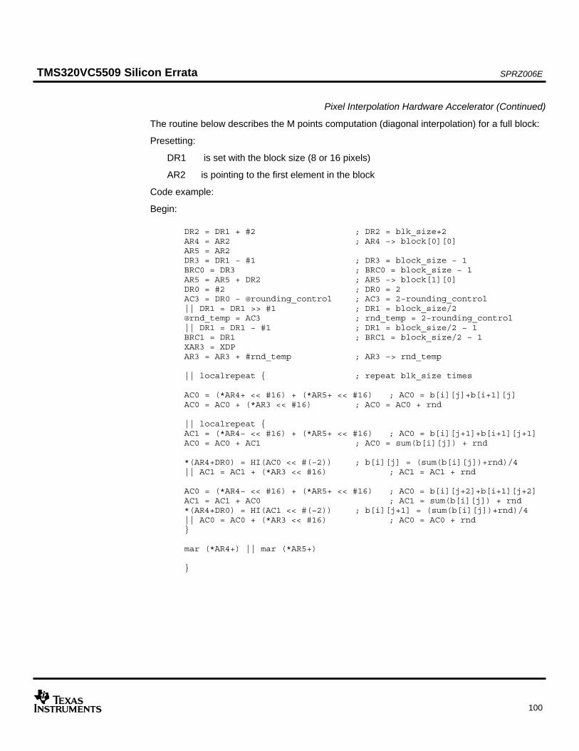
SPRZ006ETMS320VC5509 Silicon Errata
100
Pixel Interpolation Hardware Accelerator (Continued)
The routine below describes the M points computation (diagonal interpolation) for a full block:
Presetting:
DR1 is set with the block size (8 or 16 pixels)
AR2 is pointing to the first element in the block
Code example:
Begin:
DR2 = DR1 + #2 ; DR2 = blk_size+2AR4 = AR2 ; AR4 −> block[0][0]AR5 = AR2DR3 = DR1 − #1 ; DR3 = block_size − 1BRC0 = DR3 ; BRC0 = block_size − 1AR5 = AR5 + DR2 ; AR5 −> block[1][0]DR0 = #2 ; DR0 = 2AC3 = DR0 − @rounding_control ; AC3 = 2−rounding_control|| DR1 = DR1 >> #1 ; DR1 = block_size/2@rnd_temp = AC3 ; rnd_temp = 2−rounding_control|| DR1 = DR1 − #1 ; DR1 = block_size/2 − 1BRC1 = DR1 ; BRC1 = block_size/2 − 1XAR3 = XDPAR3 = AR3 + #rnd_temp ; AR3 −> rnd_temp
|| localrepeat ; repeat blk_size times
AC0 = (*AR4+ << #16) + (*AR5+ << #16) ; AC0 = b[i][j]+b[i+1][j]AC0 = AC0 + (*AR3 << #16) ; AC0 = AC0 + rnd
|| localrepeat AC1 = (*AR4− << #16) + (*AR5+ << #16) ; AC0 = b[i][j+1]+b[i+1][j+1]AC0 = AC0 + AC1 ; AC0 = sum(b[i][j]) + rnd *(AR4+DR0) = HI(AC0 << #(−2)) ; b[i][j] = (sum(b[i][j])+rnd)/4|| AC1 = AC1 + (*AR3 << #16) ; AC1 = AC1 + rnd
AC0 = (*AR4− << #16) + (*AR5+ << #16) ; AC0 = b[i][j+2]+b[i+1][j+2]AC1 = AC1 + AC0 ; AC1 = sum(b[i][j]) + rnd*(AR4+DR0) = HI(AC1 << #(−2)) ; b[i][j+1] = (sum(b[i][j])+rnd)/4|| AC0 = AC0 + (*AR3 << #16) ; AC0 = AC0 + rnd
mar (*AR4+) || mar (*AR5+)
SPRZ006ETMS320VC5509 Silicon Errata
101
3.14 Power Management Advisories
Repeated Interrupts During CPU IdleAdvisory PM_1
Revision(s) Affected: Revisions C, D, and F
Details: Any external interrupt staying low for an extended period should generate only one interrupt.The interrupt signal should normally be required to go high, then low again before additionalinterrupts would be generated. However, on the 5509, if the external interrupt stays low whilethe CPU domain enters the idle state, the associated interrupt flag is set again. This causesthe CPU to exit the idle state, and if the associated interrupt enable bit is set, the interruptservice routine will also be executed.
In case of CPU in idle and the external interrupt is driven low to wake up the CPU, repeatedinterrupt will be generated until the external interrupt signal driven high after the CPU wakesup.
When the CPU is not in idle, the interrupt responds as expected (only a single interrupt isgenerated).
Assembler Notification: None
Workaround: Limit the low pulse durations of external interrupts so that they are not still asserted when theCPU goes into idle or when waking up the CPU from idle.

SPRZ006ETMS320VC5509 Silicon Errata
102
4 Documentation Support
For device-specific data sheets and related documentation, visit the TI web site at: http://www.ti.com.
For further information regarding the TMS320VC5509, please see the latest versions of:
• TMS320C55x DSP CPU Reference Guide (literature number SPRU371)
• TMS320C55x DSP Mnemonic Instruction Set Reference Guide (literature number SPRU374)
• TMS320C55x DSP Algebraic Instruction Set Reference Guide (literature number SPRU375)
• TMS320C55x DSP Peripherals Overview Reference Guide (literature number SPRU317)
• TMS320VC5509 Fixed-Point Digital Signal Processor data manual (literature number SPRS163)
IMPORTANT NOTICE
Texas Instruments Incorporated and its subsidiaries (TI) reserve the right to make corrections, modifications,enhancements, improvements, and other changes to its products and services at any time and to discontinueany product or service without notice. Customers should obtain the latest relevant information before placingorders and should verify that such information is current and complete. All products are sold subject to TI’s termsand conditions of sale supplied at the time of order acknowledgment.
TI warrants performance of its hardware products to the specifications applicable at the time of sale inaccordance with TI’s standard warranty. Testing and other quality control techniques are used to the extent TIdeems necessary to support this warranty. Except where mandated by government requirements, testing of allparameters of each product is not necessarily performed.
TI assumes no liability for applications assistance or customer product design. Customers are responsible fortheir products and applications using TI components. To minimize the risks associated with customer productsand applications, customers should provide adequate design and operating safeguards.
TI does not warrant or represent that any license, either express or implied, is granted under any TI patent right,copyright, mask work right, or other TI intellectual property right relating to any combination, machine, or processin which TI products or services are used. Information published by TI regarding third-party products or servicesdoes not constitute a license from TI to use such products or services or a warranty or endorsement thereof.Use of such information may require a license from a third party under the patents or other intellectual propertyof the third party, or a license from TI under the patents or other intellectual property of TI.
Reproduction of information in TI data books or data sheets is permissible only if reproduction is withoutalteration and is accompanied by all associated warranties, conditions, limitations, and notices. Reproductionof this information with alteration is an unfair and deceptive business practice. TI is not responsible or liable forsuch altered documentation.
Resale of TI products or services with statements different from or beyond the parameters stated by TI for thatproduct or service voids all express and any implied warranties for the associated TI product or service andis an unfair and deceptive business practice. TI is not responsible or liable for any such statements.
Following are URLs where you can obtain information on other Texas Instruments products and applicationsolutions:
Products Applications
Amplifiers amplifier.ti.com Audio www.ti.com/audio
Data Converters dataconverter.ti.com Automotive www.ti.com/automotive
DSP dsp.ti.com Broadband www.ti.com/broadband
Interface interface.ti.com Digital Control www.ti.com/digitalcontrol
Logic logic.ti.com Military www.ti.com/military
Power Mgmt power.ti.com Optical Networking www.ti.com/opticalnetwork
Microcontrollers microcontroller.ti.com Security www.ti.com/security
Telephony www.ti.com/telephony
Video & Imaging www.ti.com/video
Wireless www.ti.com/wireless
Mailing Address: Texas Instruments
Post Office Box 655303 Dallas, Texas 75265
Copyright 2004, Texas Instruments Incorporated