TMS320DM644x DMSoC Serial Peripheral Interface … Peripheral Architecture ..... ..... 9 2.1 Clock...
37
TMS320DM644x DMSoC Serial Peripheral Interface (SPI) User's Guide Literature Number: SPRUE32A February 2007
-
Upload
dangnguyet -
Category
Documents
-
view
218 -
download
0
Transcript of TMS320DM644x DMSoC Serial Peripheral Interface … Peripheral Architecture ..... ..... 9 2.1 Clock...

TMS320DM644x DMSoCSerial Peripheral Interface (SPI)
User's Guide
Literature Number: SPRUE32A
February 2007

2 SPRUE32A–February 2007Submit Documentation Feedback

Contents
Preface ............................................................................................................................... 61 Introduction................................................................................................................ 8
1.1 Purpose of the Peripheral....................................................................................... 8
1.2 Features ........................................................................................................... 8
1.3 Functional Block Diagram....................................................................................... 9
1.4 Industry Standard(s) Compliance Statement ................................................................. 9
2 Peripheral Architecture ................................................................................................ 92.1 Clock Control ..................................................................................................... 9
2.2 Signal Descriptions ............................................................................................. 10
2.3 Pin Multiplexing ................................................................................................. 10
2.4 SPI Operation ................................................................................................... 10
2.5 Reset Considerations .......................................................................................... 17
2.6 Initialization ...................................................................................................... 17
2.7 Interrupt Support................................................................................................ 18
2.8 EDMA Event Support .......................................................................................... 19
2.9 Power Management ............................................................................................ 20
2.10 SPI Internal Loop-Back Test Mode........................................................................... 20
2.11 Emulation Considerations ..................................................................................... 20
3 Registers.................................................................................................................. 213.1 SPI Global Control Register 0 (SPIGCR0) .................................................................. 21
3.2 SPI Global Control Register 1 (SPIGCR1) .................................................................. 22
3.3 SPI Interrupt Register (SPIINT)............................................................................... 23
3.4 SPI Interrupt Level Register (SPILVL) ....................................................................... 24
3.5 SPI Flag Register (SPIFLG)................................................................................... 25
3.6 SPI Pin Control Register (SPIPC0) .......................................................................... 26
3.7 SPI Pin Control Register 2 (SPIPC2) ........................................................................ 27
3.8 SPI Shift Register (SPIDAT1)................................................................................. 28
3.9 SPI Buffer Register (SPIBUF)................................................................................. 29
3.10 SPI Emulation Register (SPIEMU) ........................................................................... 30
3.11 SPI Delay Register (SPIDELAY) ............................................................................. 31
3.12 SPI Default Chip Select Register (SPIDEF)................................................................. 32
3.13 SPI Data Format Registers (SPIFMTn)...................................................................... 33
3.14 SPI Interrupt Vector Register 0 (INTVECT0) ............................................................... 34
3.15 SPI Interrupt Vector Register 1 (INTVECT1) ............................................................... 35
Appendix A Revision History ............................................................................................. 36
SPRUE32A–February 2007 Table of Contents 3Submit Documentation Feedback

List of Figures
1 Serial Peripheral Interface (SPI) Block Diagram......................................................................... 92 Right-Aligned Transmit Data in SPIDAT1 Field of the SPI Shift Register (SPIDAT1) ............................ 113 Right-Aligned Receive Data in SPIBUF Field of the SPI Buffer Register (SPIBUF) .............................. 114 Clock Mode with POLARITY = 0 and PHASE = 0 ..................................................................... 125 Clock Mode with POLARITY = 0 and PHASE = 1 ..................................................................... 126 Clock Mode with POLARITY = 1 and PHASE = 0 ..................................................................... 137 Clock Mode with POLARITY = 1 and PHASE = 1 ..................................................................... 138 Five Bits per Character (Four-Pin Option) .............................................................................. 149 SPI Operation (3-Pin Option) ............................................................................................. 1610 SPI Operation (4-Pin Option) ............................................................................................. 1611 SPI Global Control Register 0 (SPIGCR0).............................................................................. 2112 SPI Global Control Register 1 (SPIGCR1).............................................................................. 2213 SPI Interrupt Register (SPIINT) .......................................................................................... 2314 SPI Interrupt Level Register (SPILVL)................................................................................... 2415 SPI Flag Register (SPIFLG) .............................................................................................. 2516 SPI Pin Control Register (SPIPC0) ...................................................................................... 2617 SPI Pin Control Register 2 (SPIPC2) .................................................................................... 2718 SPI Shift Register (SPIDAT1)............................................................................................. 2819 SPI Buffer Register (SPIBUF) ............................................................................................ 2920 SPI Emulation Register (SPIEMU)....................................................................................... 3021 SPI Delay Register (SPIDELAY) ......................................................................................... 3122 SPI Default Chip Select Register (SPIDEF) ............................................................................ 3223 SPI Data Format Register (SPIFMTn)................................................................................... 3324 SPI Interrupt Vector Register 0 (INTVECT0) ........................................................................... 3425 SPI Interrupt Vector Register 1 (INTVECT1) ........................................................................... 35
4 List of Figures SPRUE32A–February 2007Submit Documentation Feedback

List of Tables
1 Serial Peripheral Interface (SPI) Pins ................................................................................... 102 SPI Clocking Modes ....................................................................................................... 113 SPI Registers ............................................................................................................... 214 SPI Global Control Register 0 (SPIGCR0) Field Descriptions ....................................................... 215 SPI Global Control Register 1 (SPIGCR1) Field Descriptions ....................................................... 226 SPI Interrupt Register (SPIINT) Field Descriptions .................................................................... 237 SPI Interrupt Level Register (SPILVL) Field Descriptions ............................................................ 248 SPI Flag Register (SPIFLG) Field Descriptions ........................................................................ 259 SPI Pin Control Register (SPIPC0) Field Descriptions ................................................................ 2610 SPI Pin Control Register 2 (SPIPC2) Field Descriptions.............................................................. 2711 SPI Shift Register (SPIDAT1) Field Descriptions ...................................................................... 2812 SPI Buffer Register (SPIBUF) Field Descriptions ...................................................................... 2913 SPI Emulation Register (SPIEMU) Field Descriptions................................................................. 3014 SPI Delay Register (SPIDELAY) Field Descriptions................................................................... 3115 SPI Default Chip Select Register (SPIDEF) Field Descriptions ...................................................... 3216 SPI Data Format Register (SPIFMTn) Field Descriptions ............................................................ 3317 SPI Interrupt Vector Register 0 (INTVECT0) Field Descriptions ..................................................... 3418 SPI Interrupt Vector Register 1 (INTVECT1) Field Descriptions ..................................................... 35A-1 Document Revision History ............................................................................................... 36
SPRUE32A–February 2007 List of Tables 5Submit Documentation Feedback

PrefaceSPRUE32A–February 2007
Read This First
About This Manual
This document describes the serial peripheral interface (SPI) in the TMS320DM644x Digital MediaSystem-on-Chip (DMSoC).
Notational Conventions
This document uses the following conventions.
• Hexadecimal numbers are shown with the suffix h. For example, the following number is 40hexadecimal (decimal 64): 40h.
• Registers in this document are shown in figures and described in tables.
– Each register figure shows a rectangle divided into fields that represent the fields of the register.Each field is labeled with its bit name, its beginning and ending bit numbers above, and itsread/write properties below. A legend explains the notation used for the properties.
– Reserved bits in a register figure designate a bit that is used for future device expansion.
Related Documentation From Texas Instruments
The following documents describe the TMS320DM644x Digital Media System-on-Chip (DMSoC). Copiesof these documents are available on the Internet at www.ti.com. Tip: Enter the literature number in thesearch box provided at www.ti.com.
The current documentation that describes the DM644x DMSoC, related peripherals, and other technicalcollateral, is available in the C6000 DSP product folder at: www.ti.com/c6000.
SPRUE14 —TMS320DM644x DMSoC ARM Subsystem Reference Guide. Describes the ARMsubsystem in the TMS320DM644x Digital Media System-on-Chip (DMSoC). The ARM subsystem isdesigned to give the ARM926EJ-S (ARM9) master control of the device. In general, the ARM isresponsible for configuration and control of the device; including the DSP subsystem, the videoprocessing subsystem, and a majority of the peripherals and external memories.
SPRUE15 —TMS320DM644x DMSoC DSP Subsystem Reference Guide. Describes the digital signalprocessor (DSP) subsystem in the TMS320DM644x Digital Media System-on-Chip (DMSoC).
SPRUE19 —TMS320DM644x DMSoC Peripherals Overview Reference Guide. Provides an overviewand briefly describes the peripherals available on the TMS320DM644x Digital MediaSystem-on-Chip (DMSoC).
SPRAA84 —TMS320C64x to TMS320C64x+ CPU Migration Guide. Describes migrating from theTexas Instruments TMS320C64x digital signal processor (DSP) to the TMS320C64x+ DSP. Theobjective of this document is to indicate differences between the two cores. Functionality in thedevices that is identical is not included.
SPRU732 —TMS320C64x/C64x+ DSP CPU and Instruction Set Reference Guide. Describes the CPUarchitecture, pipeline, instruction set, and interrupts for the TMS320C64x and TMS320C64x+ digitalsignal processors (DSPs) of the TMS320C6000 DSP family. The C64x/C64x+ DSP generationcomprises fixed-point devices in the C6000 DSP platform. The C64x+ DSP is an enhancement ofthe C64x DSP with added functionality and an expanded instruction set.
SPRU871 —TMS320C64x+ DSP Megamodule Reference Guide. Describes the TMS320C64x+ digitalsignal processor (DSP) megamodule. Included is a discussion on the internal direct memory access(IDMA) controller, the interrupt controller, the power-down controller, memory protection, bandwidthmanagement, and the memory and cache.
6 Preface SPRUE32A–February 2007Submit Documentation Feedback

www.ti.com
Related Documentation From Texas Instruments
SPRAAA6 —EDMA v3.0 (EDMA3) Migration Guide for TMS320DM644x DMSoC. Describes migratingfrom the Texas Instruments TMS320C64x digital signal processor (DSP) enhanced direct memoryaccess (EDMA2) to the TMS320DM644x Digital Media System-on-Chip (DMSoC) EDMA3. Thisdocument summarizes the key differences between the EDMA3 and the EDMA2 and providesguidance for migrating from EDMA2 to EDMA3.
SPRUE32A–February 2007 Read This First 7Submit Documentation Feedback

1 Introduction
1.1 Purpose of the Peripheral
1.2 Features
User's GuideSPRUE32A–February 2007
Serial Peripheral Interface (SPI)
This document describes the serial peripheral interface (SPI) in the TMS320DM644x Digital MediaSystem-on-Chip (DMSoC).
The SPI is a high-speed synchronous serial input/output port that allows a serial bit stream of programmedlength (1 to 16 bits) to be shifted into and out of the device at a programmed bit-transfer rate. The SPI isnormally used for communication between the TMS320DM644x DMSoC and external peripherals. Typicalapplications include an interface to external I/O or peripheral expansion via devices such as shift registers,display drivers, SPI EPROMs and analog-to-digital converters.
The SPI allows serial communication with other SPI devices through a 3-pin or 4-pin mode interface. TheDM644x DMSoC implementation supports multichip-select operation for up to two SPI slave devices. TheSPI operates as a master SPI device only.
The SPI has the following features:
• 16-bit shift register• Receive buffer register• 8-bit clock prescaler• Programmable SPI clock frequency range• Programmable character length (2 to 16 bits)• Programmable clock phase (delay or no delay)• Programmable clock polarity (high or low)• Two chip select signals (SPI_EN0 and SPI_EN1) provide the ability to control two slave devices
Serial Peripheral Interface (SPI)8 SPRUE32A–February 2007Submit Documentation Feedback
www.ti.com
1.3 Functional Block Diagram
SPI_DO
SPI_DI
SPUBUF
16−bit Shift Register SPIDAT1
Control Logic and InterruptGeneration
SPI_CLK
SPI_EN0
SPI_EN1
SPIEMU
Character Length (CHARLENn)
Clock Polarity (POLARITYn)
Clock Phase (PHASEn)
Write by CPU or EDMA
Read by CPU or EDMA
Read by CPU or EDMA
Clock Prescaler(PRESCALEn)SYSCLK5
Interrupt toARM Interrupt Controller
EDMA Sync Events
16
16
16 16
16
1.4 Industry Standard(s) Compliance Statement
2 Peripheral Architecture
2.1 Clock Control
Peripheral Architecture
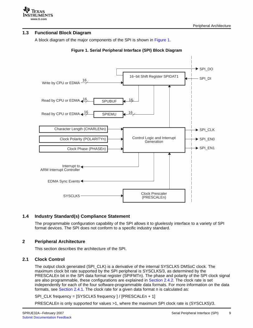
A block diagram of the major components of the SPI is shown in Figure 1.
Figure 1. Serial Peripheral Interface (SPI) Block Diagram
The programmable configuration capability of the SPI allows it to gluelessly interface to a variety of SPIformat devices. The SPI does not conform to a specific industry standard.
This section describes the architecture of the SPI.
The output clock generated (SPI_CLK) is a derivative of the internal SYSCLK5 DMSoC clock. Themaximum clock bit rate supported by the SPI peripheral is SYSCLK5/3, as determined by thePRESCALEn bit in the SPI data format register (SPIFMTn). The phase and polarity of the SPI clock signalare also programmable, these configurations are explained in Section 2.4.2. The clock rate is setindependently for each of the four software-programmable data formats. For more information on the dataformats, see Section 2.4.1. The clock rate for a given data format n is calculated as:
SPI_CLK frequency = [SYSCLK5 frequency ] / [PRESCALEn + 1]
PRESCALEn is only supported for values >1, where the maximum SPI clock rate is (SYSCLK5)/3.
SPRUE32A–February 2007 Serial Peripheral Interface (SPI) 9Submit Documentation Feedback

www.ti.com
2.2 Signal Descriptions
2.3 Pin Multiplexing
2.4 SPI Operation
2.4.1 Data Formats
Peripheral Architecture
Table 1 shows the SPI pins used to interface to external devices. SPI_CLK, SPI_DO, and SPI_DI arealways used. The SPI_EN [1:0] pins are optional and may be used if the pins are present on the slavedevice(s). The SPI_EN[1:0] pins are used to selectively enable slaves in a multiple slave system. The SPIcan be operated in a 3-pin or 4-pin mode configuration. In the 3-pin mode configuration, the SPI_EN[1:0]pins are not used.
Table 1. Serial Peripheral Interface (SPI) Pins
Pin Type Function
SPI_CLK Output Serial clock
SPI_DI Input Serial data input
SPI_DO Output Serial data output
SPI_EN0 Output Slave 0 chip select
SPI_EN1 Output Slave 1 chip select
The SPI pins are multiplexed with other device functions on the DM644x DMSoC. When the SPI serialport functions are not selected, the pins may be used as general-purpose input/output (GPIO) asdescribed in the pin multiplexing section of the device-specific data manual. In addition, the SPI_EN1 pinis also multiplexed with an ATA controller pin function.
The SPI operates as a master SPI device only. The MASTER and CLKMOD bits in the SPI global controlregister 1 (SPIGCR1) must be set to 1 for SPI module proper operation.
The SPI provides the capability to configure four independent data formats. These formats are configuredby programming the corresponding SPI data format register (SPIFMTn). In each data format, the followingcharacteristics of the SPI operation are selected:
• Character length from 2 to 16 bits: The character length is configured by the CHARLENn bit.• Shift direction (MSB first or LSB first): The shift out direction is configured by the SHIFTDIRn bit.• Clock polarity: The clock polarity is configured by the POLARITYn bit. The clock polarity is explained
in Section 2.4.2.• Clock phase: The clock phase is configured by the PHASEn bit. The clock phase formats are
explained in Section 2.4.2.
The data format is chosen on each transaction, providing the capability to use different formats withdifferent slaves. Transmit data is written to the SPI shift register (SPIDAT1) and in the same write the dataword format select (DFSEL) bit in SPIDAT1 indicates which data format is to be used for the nexttransaction. Alternatively, the data format can be configured once and applies to all transactions thatfollow until the data format is changed.
10 Serial Peripheral Interface (SPI) SPRUE32A–February 2007Submit Documentation Feedback
www.ti.com
2.4.1.1 Character Length
2.4.1.2 Shift Direction
2.4.2 Clock Polarity and Phase
Peripheral Architecture
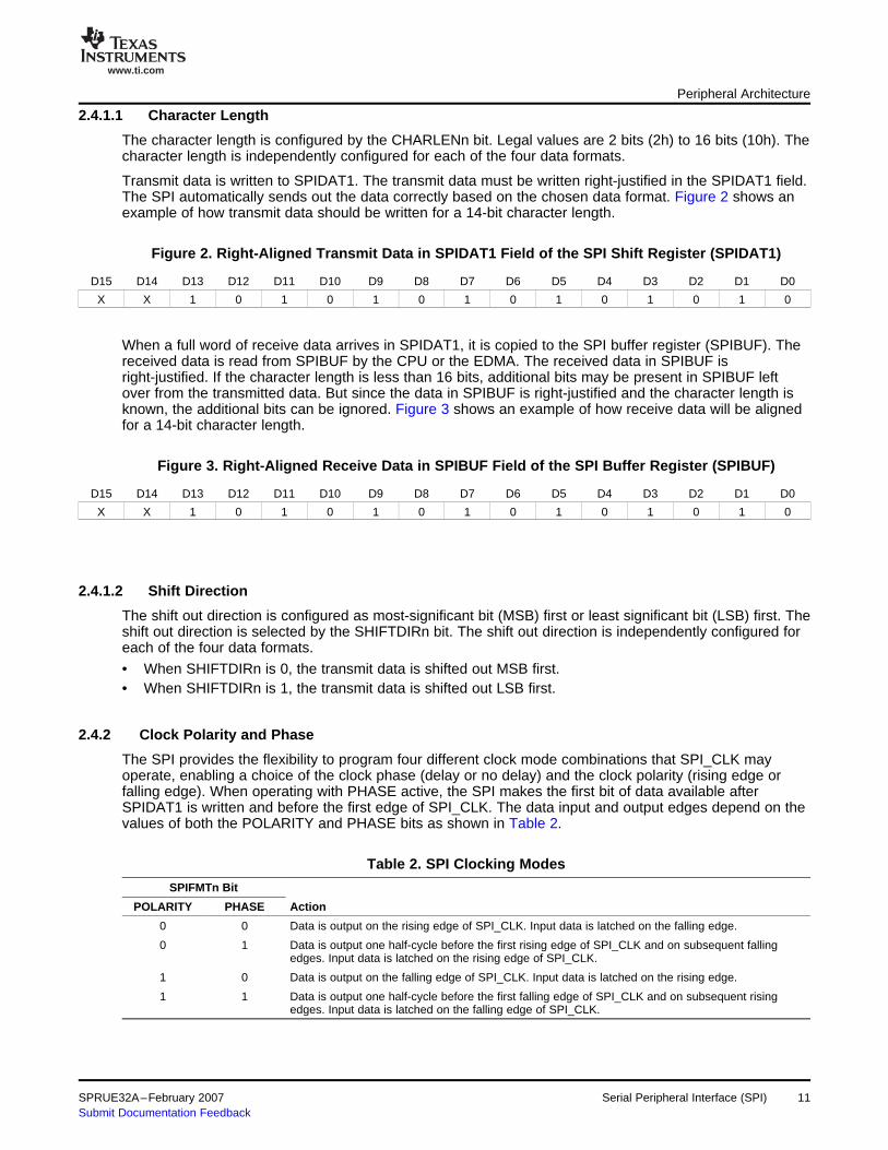
The character length is configured by the CHARLENn bit. Legal values are 2 bits (2h) to 16 bits (10h). Thecharacter length is independently configured for each of the four data formats.
Transmit data is written to SPIDAT1. The transmit data must be written right-justified in the SPIDAT1 field.The SPI automatically sends out the data correctly based on the chosen data format. Figure 2 shows anexample of how transmit data should be written for a 14-bit character length.
Figure 2. Right-Aligned Transmit Data in SPIDAT1 Field of the SPI Shift Register (SPIDAT1)
D15 D14 D13 D12 D11 D10 D9 D8 D7 D6 D5 D4 D3 D2 D1 D0
X X 1 0 1 0 1 0 1 0 1 0 1 0 1 0
When a full word of receive data arrives in SPIDAT1, it is copied to the SPI buffer register (SPIBUF). Thereceived data is read from SPIBUF by the CPU or the EDMA. The received data in SPIBUF isright-justified. If the character length is less than 16 bits, additional bits may be present in SPIBUF leftover from the transmitted data. But since the data in SPIBUF is right-justified and the character length isknown, the additional bits can be ignored. Figure 3 shows an example of how receive data will be alignedfor a 14-bit character length.
Figure 3. Right-Aligned Receive Data in SPIBUF Field of the SPI Buffer Register (SPIBUF)
D15 D14 D13 D12 D11 D10 D9 D8 D7 D6 D5 D4 D3 D2 D1 D0
X X 1 0 1 0 1 0 1 0 1 0 1 0 1 0
The shift out direction is configured as most-significant bit (MSB) first or least significant bit (LSB) first. Theshift out direction is selected by the SHIFTDIRn bit. The shift out direction is independently configured foreach of the four data formats.
• When SHIFTDIRn is 0, the transmit data is shifted out MSB first.• When SHIFTDIRn is 1, the transmit data is shifted out LSB first.
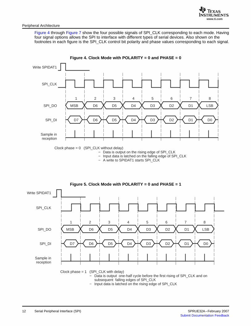
The SPI provides the flexibility to program four different clock mode combinations that SPI_CLK mayoperate, enabling a choice of the clock phase (delay or no delay) and the clock polarity (rising edge orfalling edge). When operating with PHASE active, the SPI makes the first bit of data available afterSPIDAT1 is written and before the first edge of SPI_CLK. The data input and output edges depend on thevalues of both the POLARITY and PHASE bits as shown in Table 2.
Table 2. SPI Clocking Modes
SPIFMTn Bit
POLARITY PHASE Action
0 0 Data is output on the rising edge of SPI_CLK. Input data is latched on the falling edge.
0 1 Data is output one half-cycle before the first rising edge of SPI_CLK and on subsequent fallingedges. Input data is latched on the rising edge of SPI_CLK.
1 0 Data is output on the falling edge of SPI_CLK. Input data is latched on the rising edge.
1 1 Data is output one half-cycle before the first falling edge of SPI_CLK and on subsequent risingedges. Input data is latched on the falling edge of SPI_CLK.
SPRUE32A–February 2007 Serial Peripheral Interface (SPI) 11Submit Documentation Feedback
www.ti.com
SPI_CLK
SPI_DO
SPI_DI
Sample inreception
Write SPIDAT1
1 2 3 4 5 6 7 8
MSB D6 D5 D4 D3 D2 D1 LSB
D7 D6 D5 D4 D3 D2 D1 D0
Clock phase = 0 (SPI_CLK without delay)− Data is output on the rising edge of SPI_CLK− Input data is latched on the falling edge of SPI_CLK− A write to SPIDAT1 starts SPI_CLK
SPI_CLK
SPI_DO
SPI_DI
Sample inreception
Write SPIDAT1
1 2 3 4 5 6 7 8
MSB D6 D5 D4 D3 D2 D1 LSB
D7 D6 D5 D4 D3 D2 D1 D0
Clock phase = 1 (SPI_CLK with delay)− Data is output one-half cycle before the first rising of SPI_CLK and on
subsequent falling edges of SPI_CLK− Input data is latched on the rising edge of SPI_CLK
Peripheral Architecture
Figure 4 through Figure 7 show the four possible signals of SPI_CLK corresponding to each mode. Havingfour signal options allows the SPI to interface with different types of serial devices. Also shown on thefootnotes in each figure is the SPI_CLK control bit polarity and phase values corresponding to each signal.
Figure 4. Clock Mode with POLARITY = 0 and PHASE = 0
Figure 5. Clock Mode with POLARITY = 0 and PHASE = 1
12 Serial Peripheral Interface (SPI) SPRUE32A–February 2007Submit Documentation Feedback

www.ti.com
SPI_CLK
SPI_DO
SPI_DI
Sample inreception
Write SPIDAT1
1 2 3 4 5 6 7 8
MSB D6 D5 D4 D3 D2 D1 LSB
D7 D6 D5 D4 D3 D2 D1 D0
Clock phase = 0 (SPI_CLK without delay)− Data is output on the falling edge of SPI_CLK− Input data is latched on the rising edge of SPI_CLK− A write to SPIDAT1 starts SPI_CLK
SPI_CLK
SPI_DO
SPI_DI
Sample inreception
Write SPIDAT1
1 2 3 4 5 6 7 8
MSB D6 D5 D4 D3 D2 D1 LSB
D7 D6 D5 D4 D3 D2 D1 D0
Clock phase = 1 (SPI_CLK with delay)− Data is output one-half cycle before the first falling edge of SPI_CLK
and on the subsequent rising edges of SPI_CLK− Input data is latched on the falling edge of SPI_CLK
Peripheral Architecture
Figure 6. Clock Mode with POLARITY = 1 and PHASE = 0
Figure 7. Clock Mode with POLARITY = 1 and PHASE = 1
SPRUE32A–February 2007 Serial Peripheral Interface (SPI) 13Submit Documentation Feedback

www.ti.com
7 6 5 4 3 7 6 5 4 3
7 6 5 4 3 7 6 5 34
Master SPI Interrupt flag
Slave SPI Interrupt flag
SPI_DI from slave
SPI_DO frommaster
Clock polarity = 0Clock phase = 0
Clock polarity = 0Clock phase = 1
Clock polarity = 1Clock phase = 0
Clock polarity = 1Clock phase = 1
SPI_ENx
SPI_CLK signal options:
2.4.3 Chip Select Control
2.4.3.1 Enabling Chip Selects
Peripheral Architecture
Figure 8 shows an example of an SPI data transfer between two devices using a character length of 5 bitsand the different clock mode scenarios in 4-pin mode.
Figure 8. Five Bits per Character (Four-Pin Option)
The SPI provides two chip select signals (SPI_EN0 and SPI_EN1) that are used to selectively enablemultiple slaves. The behavior of the chip selects is controlled by the CSNR and CSHOLD bits in SPIDAT1.
The CSNR bit controls which chip selects are active during the transactions that follow. This bit is used toenable either or both chip selects. To use the chip selects, the ENnFUN bit in the SPI pin control register(SPIPC0) must be set to 1 for each chip select.
Serial Peripheral Interface (SPI)14 SPRUE32A–February 2007Submit Documentation Feedback
www.ti.com
2.4.3.2 Holding Chip Selects Active Between Transactions
2.4.3.3 Programming Chip Select Setup and Hold Timing
2.4.3.4 Inactive Chip Select State Control
2.4.4 SPI Operation: 3-Pin Mode
Peripheral Architecture
Some SPI slave devices require that chip selects remain active between transactions, such as serialEEPROMs that use internal address counters, as long as the chip select is active. The CSHOLD bitcontrols whether chip selects remain asserted between transactions or not.
• When CSHOLD = 0, the chip selects are deasserted between transactions.• When CSHOLD = 1, the chip selects remain asserted between transactions as long as the chip select
information (controlled by the CSNR bits in SPIDAT1) has not changed since the last transaction. If thechip select information is altered between transactions, the chip select is deasserted even ifCSHOLD = 1.
The setup time between when the chip select signal goes active and the beginning of the transaction isprogrammable using the C2TDELAY bit in the SPI delay register (SPIDELAY). The setup time is[C2TDELAY + 2] cycles of the SYSCLK5 clock (not the SPI_CLK).
The hold time between the end of the transaction and when the chip select signal goes inactive isprogrammable using the T2CDELAY bit in SPIDELAY. The hold time is [T2CDELAY + 1] cycles of theSYSCLK5 clock (not the SPI_CLK).
If the CSHOLD function is active, the setup and hold delays are not applied between transactions wherethe chip select remains asserted.
The driven state of the chip select pins when no transaction is in progress is controlled by the ENnDEFbits in the SPI default chip select register (SPIDEF).
• When ENnDEF = 0, the corresponding chip select is driven to logic 0 when no transaction is inprogress.
• When ENnDEF = 1, the corresponding chip select is driven to logic 1 when no transaction is inprogress.
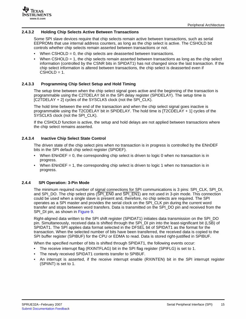
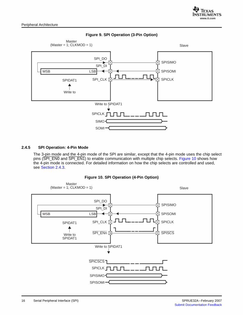
The minimum required number of signal connections for SPI communications is 3 pins: SPI_CLK, SPI_DI,and SPI_DO. The chip select pins (SPI_EN0 and SPI_EN1) are not used in 3-pin mode. This connectioncould be used when a single slave is present and, therefore, no chip selects are required. The SPIoperates as a SPI master and provides the serial clock on the SPI_CLK pin during the current wordtransfer and stops between word transfers. Data is transmitted on the SPI_DO pin and received from theSPI_DI pin, as shown in Figure 9.
Right-aligned data written to the SPI shift register (SPIDAT1) initiates data transmission on the SPI_DOpin. Simultaneously, received data is shifted through the SPI_DI pin into the least-significant bit (LSB) ofSPIDAT1. The SPI applies data format selected in the DFSEL bit of SPIDAT1 as the format for thetransaction. When the selected number of bits have been transferred, the received data is copied to theSPI buffer register (SPIBUF) for the CPU or EDMA to read. Data is stored right-justified in SPIBUF.
When the specified number of bits is shifted through SPIDAT1, the following events occur:• The receive interrupt flag (RXINTFLAG) bit in the SPI flag register (SPIFLG) is set to 1.• The newly received SPIDAT1 contents transfer to SPIBUF.• An interrupt is asserted, if the receive interrupt enable (RXINTEN) bit in the SPI interrupt register
(SPIINT) is set to 1.
SPRUE32A–February 2007 Serial Peripheral Interface (SPI) 15Submit Documentation Feedback
www.ti.com
Master(Master = 1; CLKMOD = 1)
MSB LSB
SPI_DO
SPI_DI
SPIDAT1
Write to
SPI_CLK
SPISIMO
SPISOMI
SPICLK
Slave
Write to SPIDAT1
SPICLK
SIMO
SOMI
2.4.5 SPI Operation: 4-Pin Mode
Master(Master = 1; CLKMOD = 1)
MSB LSB
SPI_DO
SPI_DI
SPIDAT1
Write toSPIDAT1
SPI_CLK
SPISIMO
SPISOMI
SPICLK
Slave
Write to SPIDAT1
SPICLK
SPISIMO
SPISOMI
SPI_ENn SPISCS
SPICSCS
Peripheral Architecture
Figure 9. SPI Operation (3-Pin Option)
The 3-pin mode and the 4-pin mode of the SPI are similar, except that the 4-pin mode uses the chip selectpins (SPI_EN0 and SPI_EN1) to enable communication with multiple chip selects. Figure 10 shows howthe 4-pin mode is connected. For detailed information on how the chip selects are controlled and used,see Section 2.4.3.
Figure 10. SPI Operation (4-Pin Option)
Serial Peripheral Interface (SPI)16 SPRUE32A–February 2007Submit Documentation Feedback

www.ti.com
2.5 Reset Considerations
2.5.1 Software Reset Considerations
2.5.2 Hardware Reset Considerations
2.6 Initialization
2.6.1 3-Pin Mode Initialization
Peripheral Architecture
This section provides the software and hardware reset considerations.
In the event of an emulator software reset, the SPI module register values are not affected.
The SPI module contains a software reset (RESET) bit in the SPI global control register 0 (SPIGCR0) thatis used to reset the SPI module. As a result of a reset, the SPI module register values go to their resetstate. The RESET bit must be set before any operation on the SPI is done.
In the event of a hardware reset, the SPI module register values go to their reset state and the applicationsoftware needs to reprogram the registers to the desired values.
There are two different methods to perform hardware reset that affects the SPI module register values.One is a full device hardware reset that resets all the device modules and the second is an individualperipheral hardware reset initiated by the Power and Sleep Controller (PSC) module. For informationabout the operation of the PSC, see the TMS320DM644x DMSoC ARM Subsystem Reference Guide(SPRUE14).
The following section provides the initialization steps to quickly get the SPI module configured for the twodifferent pin modes supported.
1. Make sure the SPI module is in reset by clearing the RESET bit in the SPI global control register 0(SPIGCR0) to 0.
2. Remove the SPI peripheral from reset by setting the RESET bit in SPIGCR0 to 1.3. Enable the CLKMOD and MASTER bits in the SPI global control register 1 (SPIGCR1).4. Enable the SPI_DI, SPI_DO, and SPI_CLK pins by setting the corresponding bits in the SPI pin control
register (SPIPC0).5. Configure the desired data format in the SPI data format register (SPIFMTn).
a. Program the clock prescale value in the PRESCALEn bit.b. Program the character size in the CHARLENn bit.c. Set the SPI clock PHASEn and POLARITYn bits.d. Set the shift direction in the SHIFTDIRn bit.
6. Select the preconfigured data format using the DFSEL bit in the SPI shift register (SPIDAT1).7. Enable the desired interrupts, if any, in the SPI interrupt register (SPIINT).8. Select whether you want the interrupt events mapped to INT0 or INT1 using the selection bits in the
SPI interrupt level register (SPILVL).9. If using the EDMA to perform the transfers, setup and enable the EDMA channels for transmit or
receive.10. Enable the SPIENA bit in SPIGCR1.11. If using the EDMA, set the DMAREQEN bit in SPIINT to 1 initiating the EDMA to start writing to
SPIDAT1; therefore, initiating the data transfer.12. Data is ready to be transferred using the CPU by writing to SPIDAT1.
SPRUE32A–February 2007 Serial Peripheral Interface (SPI) 17Submit Documentation Feedback

www.ti.com
2.6.2 4-Pin Mode Initialization
2.7 Interrupt Support
2.7.1 Interrupt Events and Requests
2.7.1.1 Receive Interrupt
Peripheral Architecture
1. Make sure the SPI module is in reset by clearing the RESET bit in the SPI global control register 0(SPIGCR0) to 0.
2. Remove the SPI peripheral from reset by setting the RESET bit in SPIGCR0 to 1.3. Enable the CLKMOD and MASTER bits in the SPI global control register 1 (SPIGCR1).4. Enable the SPI_DI, SPI_DO, and SPI_CLK pins and the necessary chip select pins (SPI_EN0 and
SPI_EN1) by setting the corresponding bits in the SPI pin control register (SPIPC0).5. Configure the desired data format in the SPI data format register (SPIFMTn).
a. Program the clock prescale value in the PRESCALEn bit.b. Program the character size in the CHARLENn bit.c. Set the SPI clock PHASEn and POLARITYn bits.d. Set the shift direction in the SHIFTDIRn bit.
6. Select the preconfigured data format using the DFSEL bit in the SPI shift register (SPIDAT1).7. If needed, configure the setup or hold time for the chip select lines using the C2TDELAY or
T2CDELAY bits in the SPI delay register (SPIDELAY).8. Select the desired chip select number. The CSNR field in SPIDAT1 defines the chip select that shall be
activated during the data transfer. Note that the SPI_ENn signals are active low.9. Setup the default chip select pin value when chip select lines are inactive using the ENnDEF bits in the
SPI default chip select register (SPIDEF).10. Enable the desired interrupts, if any, in the SPI interrupt register (SPIINT).11. Select whether you want the interrupt events mapped to INT0 or INT1 using the selection bits in the
SPI interrupt level register (SPILVL).12. If using the EDMA to perform the transfers, setup and enable the EDMA channels for transmit or
receive.13. Enable the SPIENA bit in SPIGCR1.14. If using the EDMA, set the DMAREQEN bit in SPIINT to 1 initiating the EDMA to start writing to
SPIDAT1; therefore, initiating the data transfer.15. Data is ready to be transferred using the CPU by writing to SPIDAT1.
The SPI module outputs two interrupts that are routed to the ARM CPU interrupt controller, SPIINT0 andSPIINT1. Each of the interrupt events causes a CPU interrupt on SPIINT0 or SPIINT1. The SPI interruptsystem is controlled by three registers:
• The SPI interrupt level register (SPILVL) controls which events (SPIINT0 or SPIINT1) are assigned toeach interrupt.
• The SPI interrupt register (SPIINT) contains bits to selectively enable/disable each interrupt event.• The SPI flag register (SPIFLG) contains flags indicating when each of the interrupt conditions have
occurred.
Multiple interrupt sources can be assigned to the same CPU interrupt. To identify the interrupt source inthe SPI peripheral, the CPU reads the SPI flag register (SPIFLG) or the INTVECTn code in the SPIinterrupt vector register n (IINTVECTn).
The receive interrupt occurs when a data character has been received and copied in the SPI bufferregister (SPIBUF). To enable the SPI receive interrupt, set the RXINTEN bit in the SPI interrupt register(SPIINT) to 1. To assign the receive interrupt to occur on SPIINT0, clear the RXINTLVL bit in the SPIinterrupt level register (SPILVL) to 0; to assign the receive interrupt to occur on SPIINT1, set theRXINTLVL bit in SPILVL to 1.
18 Serial Peripheral Interface (SPI) SPRUE32A–February 2007Submit Documentation Feedback
www.ti.com
2.7.1.2 Receive Overrun Interrupt
2.7.1.3 Transmit Error Interrupt
2.7.2 Interrupt Multiplexing
2.8 EDMA Event Support
Peripheral Architecture
The occurrence of the receive interrupt is recorded in the RXINTFLAG bit in the SPI flag register(SPIFLG). This flag is cleared by reading SPIBUF, writing a 1 to the RXINTFLAG bit, disabling the receiveinterrupt, or a system reset.
The receive overrun interrupt occurs when a data character has been received in the shift register beforethe previous character has been read from the SPI buffer register (SPIBUF). To enable the SPI receiveoverrun interrupt, set the OVRNINTEN bit in the SPI interrupt register (SPIINT) to 1. To assign the receiveoverrun interrupt to occur on SPIINT0, clear the OVRNINTLVL bit in the SPI interrupt level register(SPILVL) to 0; to assign the receive overrun interrupt to occur on SPIINT1, set the OVRNINTLVL bit inSPILVL to 1.
The occurrence of the receive overrun interrupt is recorded in the OVRNINTFLAG bit in the SPI flagregister (SPIFLG). This flag is cleared by writing a 1 to the OVRNINTFLAG bit, disabling the receiveoverrun interrupt, or a system reset. Reading SPIBUF does not clear the OVRNINTFLAG bit.
The transmit error interrupt occurs when the internal data transmitted does not match the external databits sensed on the SPI_DO signal. This error is used as an indication of a fault on the SPI_DO line. Toenable the SPI transmit error interrupt, set the BITERRENA bit in the SPI interrupt register (SPIINT) to 1.To assign the transmit error interrupt to occur on SPIINT0, clear the BITERRLVL bit in the SPI interruptlevel register (SPILVL) to 0; to assign the transmit error interrupt to occur on SPIINT1, set the BITERRLVLbit in SPILVL to 1.
The occurrence of the transmit error interrupt is recorded in the BITERRFLG bit in the SPI flag register(SPIFLG).
The interrupts generated by the SPI peripheral to the CPU are not multiplexed with any other interruptsources on the DM644x DMSoC.
If handling the SPI message traffic on a character-by-character basis requires too much CPU overhead,the SPI may use the system EDMA to receive or transmit data directly to or from memory.
The SPI module has two EDMA synchronization event outputs that go to the system EDMA, allowingEDMA transfers to be triggered by SPI read receive or write transmit events. SPIXEVT is a transmit syncevent; SPIREVT is a receive sync event. The SPI module enables EDMA requests by enabling the DMArequest enable (DMAREQEN) bit in the SPI interrupt register (SPIINT).
When a character is being transmitted or received, the SPI signals the EDMA via the EDMAsynchronization event signal. The EDMA controller then performs the needed data manipulation. EDMAtransfers the data from the source programmed into the SPI shift register (SPIDAT1). Data is then readfrom the SPI buffer register (SPIBUF), which automatically clears the RXINTFLAG bit in the SPI flagregister (SPIFLG).
In most cases, if the EDMA is being used to service received data from the SPI, the receive interruptenable (RXINTEN) bit in SPIINT should be cleared to 0. This prevents the CPU from both responding tothe received data in addition to the EDMA. For specific SPI synchronization event number and detailedEDMA features, refer to the TMS320DM644x DMSoC Enhanced Direct Memory Access (EDMA)Controller Reference Guide (SPRUE23).
SPRUE32A–February 2007 Serial Peripheral Interface (SPI) 19Submit Documentation Feedback
www.ti.com
2.9 Power Management
2.10 SPI Internal Loop-Back Test Mode
2.11 Emulation Considerations
Peripheral Architecture
The SPI can be placed in reduced-power modes to conserve power during periods of low activity. Thepower management of the SPI is controlled by the processor Power and Sleep Controller (PSC). The PSCacts as a master controller for power management for all of the peripherals on the device. For detailedinformation on power management procedures using the PSC, see the TMS320DM644x DMSoC ARMSubsystem Reference Guide (SPRUE14).
Since entering a low-power mode has the effect of suspending all state machine activities, care must betaken when entering such modes to ensure that a valid state is entered when low-power mode is active.As a result, application software must ensure that a low-power mode is not entered during a transmissionor reception of data.
CAUTION
The internal loop-back self-test mode should not be entered during a normaldata transaction or unpredictable operation may occur.
The internal loop-back self-test mode can be utilized to test the SPI transmit path and receive path. In thismode, the transmit signal is internally fed back to the receiver and the SPI_DO, SPI_DI, and SPI_CLKpins are disconnected. For example, the transmitted data is internally transferred to the correspondingreceive buffer while external signals remain unchanged. This mode allows the CPU to write into thetransmit buffer, and check that the receive buffer contains the correct transmit data. If an error occurs thecorresponding error is set within the status field. This capability can be useful during code developmentand debug. The loop-back test mode is enabled by setting the LOOPBACK bit in the SPI global controlregister 1 (SPIGCR1) to 1.
The SPI module does not support soft or hard stop during emulation breakpoints. The SPI module willcontinue to run if an emulation breakpoint is encountered.
During debug, read the SPI emulation register (SPIEMU) if you need to read the received data withoutotherwise altering the state of the SPI peripheral. Reading the SPI buffer register (SPIBUF) causes theflags in SPIBUF to be cleared; reading SPIEMU will read the receive data without altering the flags inSPIBUF.
Serial Peripheral Interface (SPI)20 SPRUE32A–February 2007Submit Documentation Feedback

www.ti.com
3 Registers
3.1 SPI Global Control Register 0 (SPIGCR0)
Registers
Table 3 lists the memory-mapped registers for the SPI. See the device-specific data manual for thememory address of these registers. All other register offset addresses not listed in Table 3 should beconsidered as reserved locations and the register contents should not be modified.
Table 3. SPI Registers
Offset Acronym Register Description Section
00h SPIGCR0 SPI global control register 0 Section 3.1
04h SPIGCR1 SPI global control register 1 Section 3.2
08h SPIINT SPI interrupt register Section 3.3
0Ch SPILVL SPI interrupt level register Section 3.4
10h SPIFLG SPI flag register Section 3.5
14h SPIPC0 SPI pin control register Section 3.6
1Ch SPIPC2 SPI pin control register 2 Section 3.7
3Ch SPIDAT1 SPI shift register Section 3.8
40h SPIBUF SPI buffer register Section 3.9
44h SPIEMU SPI emulation register Section 3.10
48h SPIDELAY SPI delay register Section 3.11
4Ch SPIDEF SPI default chip select register Section 3.12
50h SPIFMT0 SPI data format register 0 Section 3.13
54h SPIFMT1 SPI data format register 1 Section 3.13
58h SPIFMT2 SPI data format register 2 Section 3.13
5Ch SPIFMT3 SPI data format register 3 Section 3.13
60h INTVECT0 SPI interrupt vector register 0 Section 3.14
64h INTVECT1 SPI interrupt vector register 1 Section 3.15
The SPI global control register 0 (SPIGCR0) is shown in Figure 11 and described in Table 4.
Figure 11. SPI Global Control Register 0 (SPIGCR0)
31 16
Reserved
R-0
15 1 0
Reserved RESET
R-0 R/W-0
LEGEND: R/W = Read/Write; R = Read only; -n = value after reset
Table 4. SPI Global Control Register 0 (SPIGCR0) Field Descriptions
Bit Field Value Description
31-1 Reserved 0 Reserved. The reserved bit location is always read as 0. A value written to this field has no effect.
0 RESET Reset bit for the SPI module. RESET must be set before any operation on SPI is done.
0 SPI is in reset state.
1 SPI is out of reset state.
SPRUE32A–February 2007 Serial Peripheral Interface (SPI) 21Submit Documentation Feedback

www.ti.com
3.2 SPI Global Control Register 1 (SPIGCR1)
Registers
The SPI global control register 1 (SPIGCR1) is shown in Figure 12 and described in Table 5.
Figure 12. SPI Global Control Register 1 (SPIGCR1)
31 25 24 23 17 16
Reserved SPIENA Reserved LOOPBACK
R-0 R/W-0 R-0 R/W-0
15 2 1 0
Reserved CLKMOD MASTER
R-0 R/W-0 R/W-0
LEGEND: R/W = Read/Write; R = Read only; -n = value after reset
Table 5. SPI Global Control Register 1 (SPIGCR1) Field Descriptions
Bit Field Value Description
31-25 Reserved 0 Reserved. The reserved bit location is always read as 0. A value written to this field has no effect.
24 SPIENA SPI enable. Holds the SPI in a reset state after a chip reset. The SPI is enabled only after a 1 iswritten to this bit. This bit must be set to 1 after all other SPI configuration bits have been written.This prevents an invalid operation of the SPI while the clock polarity is being changed.
0 SPI is in reset. The RXINTFLAG and OVRNINTFLG bits in the SPI flag register (SPIFLG) are alsoheld in reset mode and forced to 0. SPI_CLK is disabled. The SPI shift register (SPIDAT1) is heldin reset mode and forced to 0.
1 Activates SPI.
23-17 Reserved 0 Reserved. The reserved bit location is always read as 0. A value written to this field has no effect.
16 LOOPBACK Internal loop-back test mode. The internal self-test option is enabled by setting this bit to 1. If theSPI_DO and SPI_DI pins are configured with SPI functionality, then the SPI_DO pin is internallyconnected to the SPI_DI pin. The transmit data is looped back as receive data and is stored in thereceive field of the concerned buffer.
Externally, during loop-back operation, the SPI_CLK pin outputs an inactive value and SPI_DIremains in a high-impedance state. The SPI has to be initialized in master mode before theloop-back is selected. If a data transfer is ongoing, errors may result.
0 Internal loop-back test mode is disabled.
1 Internal loop-back test mode is enabled.
15-2 Reserved 0 Reserved. The reserved bit location is always read as 0. This field must be written as zeroes.
1 CLKMOD Clock mode. This bit must be set for the SPI module to operate.
0 Reserved
1 SPI module clock mode is enabled.
0 MASTER Master mode. This bit must be set for the SPI module to operate.
0 Reserved
1 SPI module master mode is enabled.
Serial Peripheral Interface (SPI)22 SPRUE32A–February 2007Submit Documentation Feedback

www.ti.com
3.3 SPI Interrupt Register (SPIINT)
Registers
The SPI interrupt register (SPIINT) is shown in Figure 13 and described in Table 6.
Figure 13. SPI Interrupt Register (SPIINT)
31 17 16
Reserved DMAREQEN
R-0 R/W-0
15 9 8 7 6 5 4 3 0
Reserved RXINTEN Rsvd OVRNINTEN Rsvd BITERRENA Reserved
R-0 R/W-0 R-0 R/W-0 R-0 R/W-0 R-0
LEGEND: R/W = Read/Write; R = Read only; -n = value after reset
Table 6. SPI Interrupt Register (SPIINT) Field Descriptions
Bit Field Value Description
31-17 Reserved 0 Reserved. The reserved bit location is always read as 0. This field must be written with zeroes.
16 DMAREQEN DMA request enable. Enables the DMA request signal to be generated for both receive andtransmit channels. When using the SPI module with the EDMA, it is important that the relatedEDMA channels are configured and enabled before enabling this bit.
0 DMA is not used.
1 DMA is used.
15-9 Reserved 0 Reserved. The reserved bit location is always read as 0. A value written to this field has no effect.
8 RXINTEN Receive interrupt enable. An interrupt is generated when the RXINTFLAG bit in the SPI flag register(SPIFLG) is set by hardware; otherwise, no interrupt is generated.
0 Interrupt is not generated.
1 Interrupt is generated.
7 Reserved 0 Reserved. The reserved bit location is always read as 0. A value written to this field has no effect.
6 OVRNINTEN Overrun interrupt enable. An interrupt is generated when the OVRNINTFLG bit in the SPI flagregister (SPIFLG) is set by hardware; otherwise, no interrupt is generated.
0 Overrun interrupt is not generated.
1 Overrun interrupt is generated.
5 Reserved 0 Reserved. The reserved bit location is always read as 0. A value written to this field has no effect.
4 BITERRENA Enables interrupt on bit error.
0 No interrupt asserted upon bit error.
1 Enables an interrupt on a bit error (BITERR = 1).
3-0 Reserved 0 Reserved. The reserved bit location is always read as 0. This field must be written with zeroes.
SPRUE32A–February 2007 Serial Peripheral Interface (SPI) 23Submit Documentation Feedback

www.ti.com
3.4 SPI Interrupt Level Register (SPILVL)
Registers
The SPI interrupt level register (SPILVL) is shown in Figure 14 and described in Table 7.
Figure 14. SPI Interrupt Level Register (SPILVL)
31 16
Reserved
R-0
15 9 8 7 6 5 4 3 0
Reserved RXINTLVL Rsvd OVRNINTLVL Rsvd BITERRLVL Reserved
R-0 R/W-0 R-0 R/W-0 R-0 R/W-0 R-0
LEGEND: R/W = Read/Write; R = Read only; -n = value after reset
Table 7. SPI Interrupt Level Register (SPILVL) Field Descriptions
Bit Field Value Description
31-9 Reserved 0 Reserved. The reserved bit location is always read as 0. A value written to this field has no effect.
8 RXINTLVL Receive interrupt level.
0 Receive interrupt is mapped to interrupt line INT0.
1 Receive interrupt is mapped to interrupt line INT1.
7 Reserved 0 Reserved. The reserved bit location is always read as 0. A value written to this field has no effect.
6 OVRNINTLVL Receive overrun interrupt level.
0 Receive overrun interrupt is mapped to interrupt line INT0.
1 Receive overrun interrupt is mapped to interrupt line INT1.
5 Reserved 0 Reserved. The reserved bit location is always read as 0. A value written to this field has no effect.
4 BITERRLVL Bit error interrupt level.
0 Bit error interrupt is mapped to interrupt line INT0.
1 Bit error interrupt is mapped to interrupt line INT1.
3-0 Reserved 0 Reserved. The reserved bit location is always read as 0. This field must be written with zeroes.
Serial Peripheral Interface (SPI)24 SPRUE32A–February 2007Submit Documentation Feedback
www.ti.com
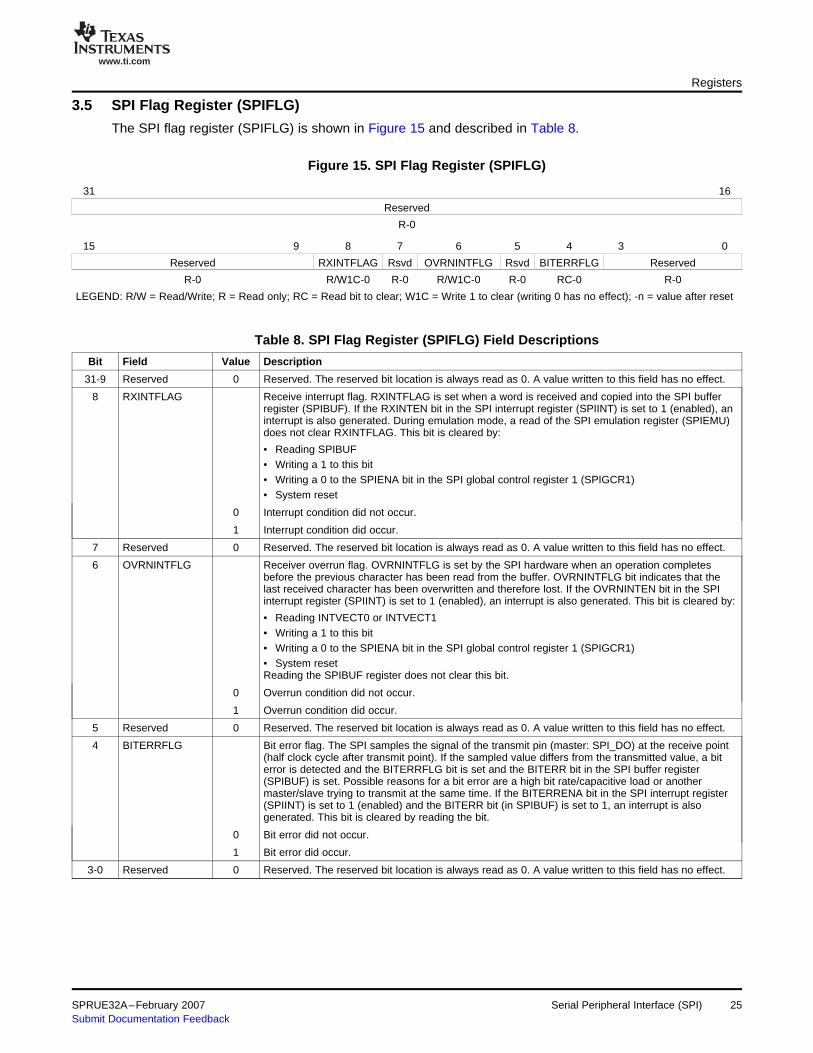
3.5 SPI Flag Register (SPIFLG)
Registers
The SPI flag register (SPIFLG) is shown in Figure 15 and described in Table 8.
Figure 15. SPI Flag Register (SPIFLG)
31 16
Reserved
R-0
15 9 8 7 6 5 4 3 0
Reserved RXINTFLAG Rsvd OVRNINTFLG Rsvd BITERRFLG Reserved
R-0 R/W1C-0 R-0 R/W1C-0 R-0 RC-0 R-0
LEGEND: R/W = Read/Write; R = Read only; RC = Read bit to clear; W1C = Write 1 to clear (writing 0 has no effect); -n = value after reset
Table 8. SPI Flag Register (SPIFLG) Field Descriptions
Bit Field Value Description
31-9 Reserved 0 Reserved. The reserved bit location is always read as 0. A value written to this field has no effect.
8 RXINTFLAG Receive interrupt flag. RXINTFLAG is set when a word is received and copied into the SPI bufferregister (SPIBUF). If the RXINTEN bit in the SPI interrupt register (SPIINT) is set to 1 (enabled), aninterrupt is also generated. During emulation mode, a read of the SPI emulation register (SPIEMU)does not clear RXINTFLAG. This bit is cleared by:
• Reading SPIBUF• Writing a 1 to this bit• Writing a 0 to the SPIENA bit in the SPI global control register 1 (SPIGCR1)• System reset
0 Interrupt condition did not occur.
1 Interrupt condition did occur.
7 Reserved 0 Reserved. The reserved bit location is always read as 0. A value written to this field has no effect.
6 OVRNINTFLG Receiver overrun flag. OVRNINTFLG is set by the SPI hardware when an operation completesbefore the previous character has been read from the buffer. OVRNINTFLG bit indicates that thelast received character has been overwritten and therefore lost. If the OVRNINTEN bit in the SPIinterrupt register (SPIINT) is set to 1 (enabled), an interrupt is also generated. This bit is cleared by:
• Reading INTVECT0 or INTVECT1• Writing a 1 to this bit• Writing a 0 to the SPIENA bit in the SPI global control register 1 (SPIGCR1)• System resetReading the SPIBUF register does not clear this bit.
0 Overrun condition did not occur.
1 Overrun condition did occur.
5 Reserved 0 Reserved. The reserved bit location is always read as 0. A value written to this field has no effect.
4 BITERRFLG Bit error flag. The SPI samples the signal of the transmit pin (master: SPI_DO) at the receive point(half clock cycle after transmit point). If the sampled value differs from the transmitted value, a biterror is detected and the BITERRFLG bit is set and the BITERR bit in the SPI buffer register(SPIBUF) is set. Possible reasons for a bit error are a high bit rate/capacitive load or anothermaster/slave trying to transmit at the same time. If the BITERRENA bit in the SPI interrupt register(SPIINT) is set to 1 (enabled) and the BITERR bit (in SPIBUF) is set to 1, an interrupt is alsogenerated. This bit is cleared by reading the bit.
0 Bit error did not occur.
1 Bit error did occur.
3-0 Reserved 0 Reserved. The reserved bit location is always read as 0. A value written to this field has no effect.
SPRUE32A–February 2007 Serial Peripheral Interface (SPI) 25Submit Documentation Feedback
www.ti.com
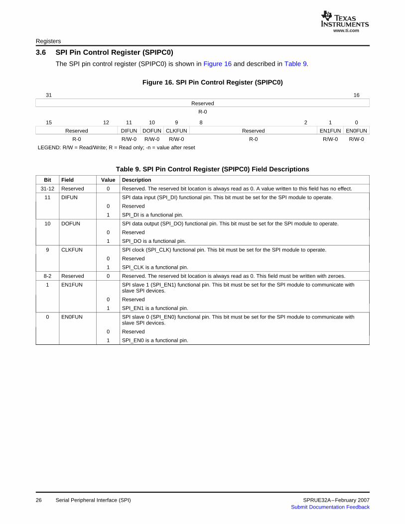
3.6 SPI Pin Control Register (SPIPC0)
Registers
The SPI pin control register (SPIPC0) is shown in Figure 16 and described in Table 9.
Figure 16. SPI Pin Control Register (SPIPC0)
31 16
Reserved
R-0
15 12 11 10 9 8 2 1 0
Reserved DIFUN DOFUN CLKFUN Reserved EN1FUN EN0FUN
R-0 R/W-0 R/W-0 R/W-0 R-0 R/W-0 R/W-0
LEGEND: R/W = Read/Write; R = Read only; -n = value after reset
Table 9. SPI Pin Control Register (SPIPC0) Field Descriptions
Bit Field Value Description
31-12 Reserved 0 Reserved. The reserved bit location is always read as 0. A value written to this field has no effect.
11 DIFUN SPI data input (SPI_DI) functional pin. This bit must be set for the SPI module to operate.
0 Reserved
1 SPI_DI is a functional pin.
10 DOFUN SPI data output (SPI_DO) functional pin. This bit must be set for the SPI module to operate.
0 Reserved
1 SPI_DO is a functional pin.
9 CLKFUN SPI clock (SPI_CLK) functional pin. This bit must be set for the SPI module to operate.
0 Reserved
1 SPI_CLK is a functional pin.
8-2 Reserved 0 Reserved. The reserved bit location is always read as 0. This field must be written with zeroes.
1 EN1FUN SPI slave 1 (SPI_EN1) functional pin. This bit must be set for the SPI module to communicate withslave SPI devices.
0 Reserved
1 SPI_EN1 is a functional pin.
0 EN0FUN SPI slave 0 (SPI_EN0) functional pin. This bit must be set for the SPI module to communicate withslave SPI devices.
0 Reserved
1 SPI_EN0 is a functional pin.
Serial Peripheral Interface (SPI)26 SPRUE32A–February 2007Submit Documentation Feedback
www.ti.com
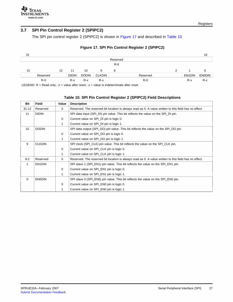
3.7 SPI Pin Control Register 2 (SPIPC2)
Registers
The SPI pin control register 2 (SPIPC2) is shown in Figure 17 and described in Table 10.
Figure 17. SPI Pin Control Register 2 (SPIPC2)
31 16
Reserved
R-0
15 12 11 10 9 8 2 1 0
Reserved DIDIN DODIN CLKDIN Reserved EN1DIN EN0DIN
R-0 R-x R-x R-x R-0 R-x R-x
LEGEND: R = Read only; -n = value after reset; -x = value is indeterminate after reset
Table 10. SPI Pin Control Register 2 (SPIPC2) Field Descriptions
Bit Field Value Description
31-12 Reserved 0 Reserved. The reserved bit location is always read as 0. A value written to this field has no effect.
11 DIDIN SPI data input (SPI_DI) pin value. This bit reflects the value on the SPI_DI pin.
0 Current value on SPI_DI pin is logic 0.
1 Current value on SPI_DI pin is logic 1.
10 DODIN SPI data output (SPI_DO) pin value. This bit reflects the value on the SPI_DO pin.
0 Current value on SPI_DO pin is logic 0.
1 Current value on SPI_DO pin is logic 1.
9 CLKDIN SPI clock (SPI_CLK) pin value. This bit reflects the value on the SPI_CLK pin.
0 Current value on SPI_CLK pin is logic 0.
1 Current value on SPI_CLK pin is logic 1.
8-2 Reserved 0 Reserved. The reserved bit location is always read as 0. A value written to this field has no effect.
1 EN1DIN SPI slave 1 (SPI_EN1) pin value. This bit reflects the value on the SPI_EN1 pin.
0 Current value on SPI_EN1 pin is logic 0.
1 Current value on SPI_EN1 pin is logic 1.
0 EN0DIN SPI slave 0 (SPI_EN0) pin value. This bit reflects the value on the SPI_EN0 pin.
0 Current value on SPI_EN0 pin is logic 0.
1 Current value on SPI_EN0 pin is logic 1.
SPRUE32A–February 2007 Serial Peripheral Interface (SPI) 27Submit Documentation Feedback

www.ti.com
3.8 SPI Shift Register (SPIDAT1)
Registers
The SPI shift register (SPIDAT1) is shown in Figure 18 and described in Table 11.
Figure 18. SPI Shift Register (SPIDAT1)
31 29 28 27 26 25 24 23 18 17 16
Reserved CSHOLD Reserved DFSEL Reserved CSNR
R-0 R/W-0 R-0 R/W-0 R-0 R/W-0
15 0
SPIDAT1
R/W-0
LEGEND: R/W = Read/Write; R = Read only; -n = value after reset
Table 11. SPI Shift Register (SPIDAT1) Field Descriptions
Bit Field Value Description
31-29 Reserved 0 Reserved. The reserved bit location is always read as 0. A value written to this field has no effect.
28 CSHOLD Chip select hold mode. CSHOLD is considered in 4-pin mode only. CSHOLD defines the behaviorof the chip select line at the end of a transfer.
0 Chip select signal is deactivated at the end of a transfer after the T2CDELAY time has passed. Iftwo consecutive transfers are dedicated to the same chip select, this chip select signal is shortlydeactivated before it is activated again.
1 Chip select signal is held active at the end of a transfer until a control field with new data andcontrol information is loaded into the SPIDAT1 bit. If the new chip select information equals theprevious information, the active chip select signal is extended until the end of transfer withCSHOLD cleared or until the chip select information changes.
27-26 Reserved 0 Reserved. The reserved bit location is always read as 0. This field must be written with zeroes.
25-24 DFSEL 0-3h Data word format select.
0 Data format 0 is selected.
1h Data format 1 is selected.
2h Data format 2 is selected.
3h Data format 3 is selected.
23-18 Reserved 0 Reserved. The reserved bit location is always read as 0. A value written to this field has no effect.
17-16 CSNR 0-3h Chip select number. CSNR defines the chip select that shall be activated during the data transfer.Note that the SPI_ENn signals are active low.
0 Both chip select SPI_EN0 and SPI_EN1 are selected.
1h Chip select SPI_EN1 is selected only.
2h Chip select SPI_EN0 is selected only.
3h No chip select is used.
15-0 SPIDAT1 0-FFFFh SPI shift data 1. This field makes up the SPI shift register. Data is shifted out of the MSB (bit 15)and into the LSB (bit 0). The SPIENA bit in the SPI global control register 1 (SPIGCR1) must beset to 1 before this register can be written to. Writing a 0 to the SPIENA bit forces the SPIDAT1 bitto 0.
A write to this field drives the SPI_EN[1:0] signal low if the SPI_EN[1:0] signals are enabled in theSPI pin control register (SPIPC0).
When data is read from this field, the value is indeterminate because of the shift operation. Thevalue in the SPI buffer register (SPIBUF) should be read after the shift operation is complete todetermine what data was shifted into SPIDAT1.
Serial Peripheral Interface (SPI)28 SPRUE32A–February 2007Submit Documentation Feedback

www.ti.com
3.9 SPI Buffer Register (SPIBUF)
Registers
The SPI buffer register (SPIBUF) is shown in Figure 19 and described in Table 12. Reading SPIBUFclears the OVRNINTFLG and RXINTFLAG bits in the SPI flag register (SPIFLG).
Figure 19. SPI Buffer Register (SPIBUF)
31 30 29 28 27 18 17 16
RXEMPTY RXOVR TXFULL BITERR Reserved LCSNR
R-1 RC-0 R-0 RC-0 R-0 R-0
15 0
SPIBUF
R-x
LEGEND: R/W = Read/Write; R = Read only; RC = Read bit to clear; -n = value after reset; -x = value is indeterminate after reset
Table 12. SPI Buffer Register (SPIBUF) Field Descriptions
Bit Field Value Description
31 RXEMPTY Receive data buffer empty. This is a read-only flag. When the host reads an SPIBUF field or theentire SPIBUF, this automatically sets the RXEMPTY bit. When a data transfer has been finishedand the received data is copied into SPIBUF, the RXEMPTY bit is cleared.
0 Data is received and copied into an SPIBUF field.
1 No data received since last reading SPIBUF.
30 RXOVR Receive data buffer overrun. This is a read-to-clear only flag, that is, reading this bit automaticallyclears the bit. When a data transfer has been finished and the received data is copied into SPIBUFwith the RXEMPTY bit already cleared, the RXOVR bit is set.
0 No receive data overrun condition occurred since last time reading the status field.
1 A receive data overrun condition occurred since last time reading the status field.
29 TXFULL Transmit data buffer full. This is a read-only flag. Writing into SPIDAT1 bits in the SPI shift register(SPIDAT1) automatically sets the TXFULL bit. After transfer of the transmit data the TXFULL flagis cleared.
0 No new transmit data from the host since previous transfer of transmit data.
1 Host provided new transmit data to SPIDAT1.
28 BITERR Bit error. This is a read-to-clear only flag, that is, reading this bit automatically clears the bit. Thisbit represents a copy of the BITERRFLG bit in the SPI flag register (SPIFLG). The SPI samplesthe signal of the transmit pin (master: SIMO, slave: SOMI) at the receive point (half clock cycleafter transmit point). If the sampled value differs from the transmitted value, a bit error is detectedand the BITERRFLG bit is set and the BITERR bit is set. Possible reasons for a bit error are ahigh bit rate/capacitive load or another master/slave trying to transmit at the same time. If theBITERRENA bit in the SPI interrupt register (SPIINT) is set to 1 (enabled) and the BITERR bit isset to 1, an interrupt is also generated.
0 Bit error did not occur.
1 Bit error did occur.
27-18 Reserved 0 Reserved. The reserved bit location is always read as 0. A value written to this field has no effect.
17-16 LCSNR 0-3h Last chip select number. LCSNR in the status field is a copy of the CSNR bit in the correspondingcontrol field. It defines the chip select that has been activated during the last data transfer from thecorresponding buffer. LCSNR is copied after transmission during write back of received data.
15-0 SPIBUF 0-FFFFh SPI receive buffer. This field makes up the SPI receive buffer. Data in this field is the datareceived via the SPI_DI pin and transferred from the SPIDAT1 bits in the SPI shift register(SPIDAT1). Since the data is shifted into the SPI with the most-significant bit first, for word lengthsless than 16, the data is stored right-justified in the register.
SPRUE32A–February 2007 Serial Peripheral Interface (SPI) 29Submit Documentation Feedback

www.ti.com
3.10 SPI Emulation Register (SPIEMU)
Registers
The SPI emulation register (SPIEMU) is shown in Figure 20 and described in Table 13.
Figure 20. SPI Emulation Register (SPIEMU)
31 16
Reserved
R-0
15 0
SPIEMU
R-x
LEGEND: R = Read only; -n = value after reset; -x = value is indeterminate after reset
Table 13. SPI Emulation Register (SPIEMU) Field Descriptions
Bit Field Value Description
31-16 Reserved 0 Reserved. The reserved bit location is always read as 0. A value written to this field has no effect.
15-0 SPIEMU 0-FFFFh SPI emulation. SPI emulation is a mirror of the SPI buffer register (SPIBUF). The only differencebetween SPIEMU and SPIBUF is that a read from SPIEMU does not clear the OVRNINTFLG andRXINTFLAG bits in the SPI flag register (SPIFLG).
Serial Peripheral Interface (SPI)30 SPRUE32A–February 2007Submit Documentation Feedback

www.ti.com
3.11 SPI Delay Register (SPIDELAY)
SCS
CLK
SOMI
tC2TDELAY
SYSCLK5
tC2TDELAY�C2TDELAYSYSCLK5
� 2
SCS
CLK
SOMI
tT2CDELAY
SYSCLK5
tT2CDELAY�T2CDELAYSYSCLK5
� 1
Registers
The SPI delay register (SPIDELAY) is shown in Figure 21 and described in Table 14.
Figure 21. SPI Delay Register (SPIDELAY)
31 29 28 24 23 21 20 16
Reserved C2TDELAY Reserved T2CDELAY
R-0 R/W-0 R-0 R/W-0
15 0
Reserved
R/W-0
LEGEND: R/W = Read/Write; R = Read only; -n = value after reset
Table 14. SPI Delay Register (SPIDELAY) Field Descriptions
Bit Field Value Description
31-29 Reserved 0 Reserved. The reserved bit location is always read as 0. A value written to this field has no effect.
28-24 C2TDELAY 0-16h Chip-select-active-to-transmit-start-delay. C2TDELAY defines a setup time for the slave device thatdelays the data transmission from the chip select active edge by a multiple of SYSCLK5 clock cycles.C2TDELAY is configured between 2 and 22 SYSCLK5 clock cycles.
The setup time value is calculated as:
Example: SYSCLK5 = 25 MHz and C2TDELAY = 06h; therefore, tC2TDELAY = 320 ns. When the chipselect signal becomes active, the slave has to prepare data transfer within 320 ns.
23-21 Reserved 0 Reserved. The reserved bit location is always read as 0. A value written to this field has no effect.
20-16 T2CDELAY 0-16h Transmit-end-to-chip-select-inactive-delay. T2CDELAY defines a hold time for the slave device thatdelays the chip select deactivation by a multiple of SYSCLK5 clock cycles after the last bit istransferred. T2CDELAY is configured between 1 and 22 SYSCLK5 clock cycles.
The hold time value is calculated as:
Example: SYSCLK5 = 25 MHz and T2CDELAY = 02h; therefore, tT2CDELAY = 120 ns. After the last databit is being transferred, the chip select signal is held active for 120 ns.
15-0 Reserved 0 Reserved. The reserved bit location is always read as 0. This field must be written with zeroes.
SPRUE32A–February 2007 Serial Peripheral Interface (SPI) 31Submit Documentation Feedback

www.ti.com
3.12 SPI Default Chip Select Register (SPIDEF)
Registers
The SPI default chip select register (SPIDEF) is shown in Figure 22 and described in Table 15.
Figure 22. SPI Default Chip Select Register (SPIDEF)
31 16
Reserved
R-0
15 2 1 0
Reserved EN1DEF EN0DEF
R-0 R/W-1 R/W-1
LEGEND: R/W = Read/Write; R = Read only; -n = value after reset
Table 15. SPI Default Chip Select Register (SPIDEF) Field Descriptions
Bit Field Value Description
31-2 Reserved 0 Reserved. The reserved bit location is always read as 0. A value written to this field has no effect.
1 EN1DEF Chip select default pattern. Selects the output to the slave 1 chip select pin (SPI_EN1) when notransmission is currently in progress. EN1DEF allows you to set a chip select pattern that deselects allthe SPI slaves.
0 SPI_EN1 is driven to logic 0 when no transaction is in progress.
1 SPI_EN1 is driven to logic 1 when no transaction is in progress.
0 EN0DEF Chip select default pattern. Selects the output to the slave 0 chip select pin (SPI_EN0) when notransmission is currently in progress. EN0DEF allows you to set a chip select pattern that deselects allthe SPI slaves.
0 SPI_EN0 is driven to logic 0 when no transaction is in progress.
1 SPI_EN0 is driven to logic 1 when no transaction is in progress.
Serial Peripheral Interface (SPI)32 SPRUE32A–February 2007Submit Documentation Feedback

www.ti.com
3.13 SPI Data Format Registers (SPIFMTn)
SPI_CLK� SYSCLK5(PRESCALEn� 1)
Registers
The SPI data format register (SPIFMT0, SPIFMT1, SPIFMT2, and SPIFMT3) is shown in Figure 23 anddescribed in Table 16.
Figure 23. SPI Data Format Register (SPIFMTn)
31 21 20 19 18 17 16
Reserved SHIFTDIRn Reserved POLARITYn PHASEn
R/W-0 R/W-0 R-0 R/W-0 R/W-0
15 8 7 5 4 0
PRESCALEn Reserved CHARLENn
R/W-0 R-0 R/W-0
LEGEND: R/W = Read/Write; R = Read only; -n = value after reset
Table 16. SPI Data Format Register (SPIFMTn) Field Descriptions
Bit Field Value Description
31-21 Reserved 0 Reserved. The reserved bit location is always read as 0. This field must be written with zeroes.
20 SHIFTDIRn Shift direction for data format n. SHIFTDIRn selects the shift direction for data format n (n = 1,2,3).
0 Most-significant bit is shifted out first.
1 Least-significant bit is shifted out first.
19-18 Reserved 0 Reserved. The reserved bit location is always read as 0. A value written to this field has no effect.
17 POLARITYn Clock polarity for data format n. POLARITYn defines the clock polarity for data format n(n = 1,2,3).
0 SPI clock signal is low-inactive, that is, before and after data transfer the clock signal is low.
1 SPI clock signal is high-inactive, that is, before and after data transfer the clock signal is high.
16 PHASEn Clock delay for data format n. PHASEn defines the clock delay for data format n (n = 1,2,3).
0 SPI clock signal is not delayed versus the transmit/receive data stream. The first data bit istransmitted with the first clock edge and the first bit is received with the second (inverse) clockedge.
1 SPI clock signal is delayed by a half SPI clock cycle versus the transmit/receive data stream. Thefirst transmit bit has to output prior to the first clock edge. Master and slave receive the first bit withthe first edge.
15-8 PRESCALEn 2-FFh Prescaler for data format n. PRESCALEn defines the bit transfer rate for data format n (n = 1,2,3).PRESCALEn is directly derived from SYSCLK5 CLK. The clock rate is calculated as:
PRESCALEn is only supported for values >1, where the maximum SPI clock rate is SYSCLK5/3.
7-5 Reserved 0 Reserved. The reserved bit location is always read as 0. A value written to this field has no effect.
4-0 CHARLENn 0-1Fh Data word length for data format n. CHARLENn defines the word length for data format n(n = 1,2,3). Legal values are 2h (data word length = 2 bits) to 10h (data word length = 16 bits).Other values, such as 0 or 1Fh, are not detected and their effect is indeterminate.
0-1h Not detected and their effect is indeterminate.
2h-10h Data word length is 2 bits to 16 bits.
11h-1Fh Not detected and their effect is indeterminate.
SPRUE32A–February 2007 Serial Peripheral Interface (SPI) 33Submit Documentation Feedback
www.ti.com
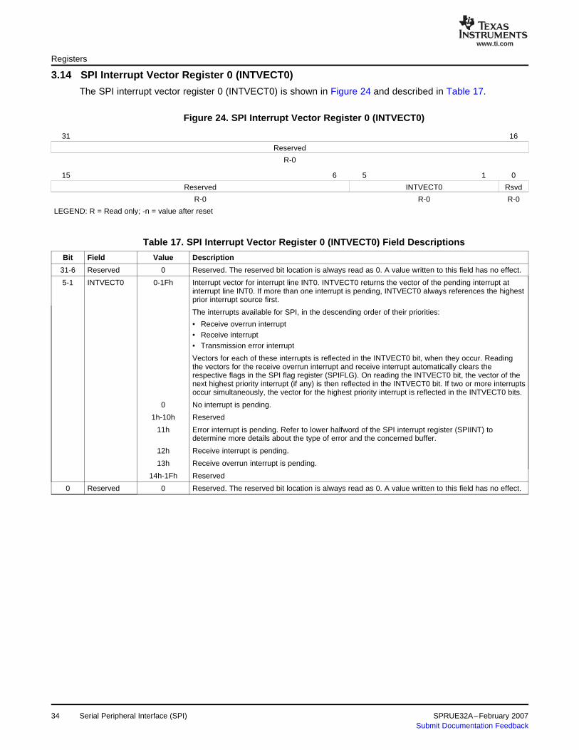
3.14 SPI Interrupt Vector Register 0 (INTVECT0)
Registers
The SPI interrupt vector register 0 (INTVECT0) is shown in Figure 24 and described in Table 17.
Figure 24. SPI Interrupt Vector Register 0 (INTVECT0)
31 16
Reserved
R-0
15 6 5 1 0
Reserved INTVECT0 Rsvd
R-0 R-0 R-0
LEGEND: R = Read only; -n = value after reset
Table 17. SPI Interrupt Vector Register 0 (INTVECT0) Field Descriptions
Bit Field Value Description
31-6 Reserved 0 Reserved. The reserved bit location is always read as 0. A value written to this field has no effect.
5-1 INTVECT0 0-1Fh Interrupt vector for interrupt line INT0. INTVECT0 returns the vector of the pending interrupt atinterrupt line INT0. If more than one interrupt is pending, INTVECT0 always references the highestprior interrupt source first.
The interrupts available for SPI, in the descending order of their priorities:
• Receive overrun interrupt• Receive interrupt• Transmission error interrupt
Vectors for each of these interrupts is reflected in the INTVECT0 bit, when they occur. Readingthe vectors for the receive overrun interrupt and receive interrupt automatically clears therespective flags in the SPI flag register (SPIFLG). On reading the INTVECT0 bit, the vector of thenext highest priority interrupt (if any) is then reflected in the INTVECT0 bit. If two or more interruptsoccur simultaneously, the vector for the highest priority interrupt is reflected in the INTVECT0 bits.
0 No interrupt is pending.
1h-10h Reserved
11h Error interrupt is pending. Refer to lower halfword of the SPI interrupt register (SPIINT) todetermine more details about the type of error and the concerned buffer.
12h Receive interrupt is pending.
13h Receive overrun interrupt is pending.
14h-1Fh Reserved
0 Reserved 0 Reserved. The reserved bit location is always read as 0. A value written to this field has no effect.
Serial Peripheral Interface (SPI)34 SPRUE32A–February 2007Submit Documentation Feedback

www.ti.com
3.15 SPI Interrupt Vector Register 1 (INTVECT1)
Registers
The SPI interrupt vector register 1 (INTVECT1) is shown in Figure 25 and described in Table 18.
Figure 25. SPI Interrupt Vector Register 1 (INTVECT1)
31 16
Reserved
R-0
15 6 5 1 0
Reserved INTVECT1 Rsvd
R-0 R-0 R-0
LEGEND: R = Read only; -n = value after reset
Table 18. SPI Interrupt Vector Register 1 (INTVECT1) Field Descriptions
Bit Field Value Description
31-6 Reserved 0 Reserved. The reserved bit location is always read as 0. A value written to this field has no effect.
5-1 INTVECT1 0-1Fh Interrupt vector for interrupt line INT1. INTVECT1 returns the vector of the pending interrupt atinterrupt line INT1. If more than one interrupt is pending, INTVECT1 always references the highestprior interrupt source first.
The interrupts available for SPI, in the descending order of their priorities:
• Receive overrun interrupt• Receive interrupt• Transmission error interrupt
Vectors for each of these interrupts is reflected in the INTVECT1 bit, when they occur. Readingthe vectors for the receive overrun interrupt and receive interrupt automatically clears therespective flags in the SPI flag register (SPIFLG). On reading the INTVECT1 bit, the vector of thenext highest priority interrupt (if any) is then reflected in the INTVECT1 bit. If two or more interruptsoccur simultaneously, the vector for the highest priority interrupt is reflected in the INTVECT1 bits.
0 No interrupt is pending.
1h-10h Reserved
11h Error interrupt is pending. Refer to lower halfword of the SPI interrupt register (SPIINT) todetermine more details about the type of error and the concerned buffer.
12h Receive interrupt is pending.
13h Receive overrun interrupt is pending.
14h-1Fh Reserved
0 Reserved 0 Reserved. The reserved bit location is always read as 0. A value written to this field has no effect.
SPRUE32A–February 2007 Serial Peripheral Interface (SPI) 35Submit Documentation Feedback

www.ti.com
Appendix A Revision History
Table A-1 lists the changes made since the previous version of this document.
Table A-1. Document Revision History
Reference Additions/Modifications/Deletions
Section 2.1 Changed first paragraph.
Section 2.6 Changed subsection.
Table 14 Changed clock signal name in waveform of C2TDELAY and T2CDELAY bits.
Table 16 Changed Description for PRESCALEn (bit 15-8).
36 Revision History SPRUE32A–February 2007Submit Documentation Feedback

IMPORTANT NOTICE
Texas Instruments Incorporated and its subsidiaries (TI) reserve the right to make corrections, modifications, enhancements, improvements, and other changes to its products and services at any time and to discontinue any product or service without notice. Customers should obtain the latest relevant information before placing orders and should verify that such information is current and complete. All products are sold subject to TI’s terms and conditions of sale supplied at the time of order acknowledgment. TI warrants performance of its hardware products to the specifications applicable at the time of sale in accordance with TI’s standard warranty. Testing and other quality control techniques are used to the extent TI deems necessary to support this warranty. Except where mandated by government requirements, testing of all parameters of each product is not necessarily performed. TI assumes no liability for applications assistance or customer product design. Customers are responsible for their products and applications using TI components. To minimize the risks associated with customer products and applications, customers should provide adequate design and operating safeguards. TI does not warrant or represent that any license, either express or implied, is granted under any TI patent right, copyright, mask work right, or other TI intellectual property right relating to any combination, machine, or process in which TI products or services are used. Information published by TI regarding third-party products or services does not constitute a license from TI to use such products or services or a warranty or endorsement thereof. Use of such information may require a license from a third party under the patents or other intellectual property of the third party, or a license from TI under the patents or other intellectual property of TI. Reproduction of information in TI data books or data sheets is permissible only if reproduction is without alteration and is accompanied by all associated warranties, conditions, limitations, and notices. Reproduction of this information with alteration is an unfair and deceptive business practice. TI is not responsible or liable for such altered documentation. Resale of TI products or services with statements different from or beyond the parameters stated by TI for that product or service voids all express and any implied warranties for the associated TI product or service and is an unfair and deceptive business practice. TI is not responsible or liable for any such statements. Following are URLs where you can obtain information on other Texas Instruments products and application solutions: Products Applications Amplifiers amplifier.ti.com Audio www.ti.com/audio Data Converters dataconverter.ti.com Automotive www.ti.com/automotive DSP dsp.ti.com Broadband www.ti.com/broadband Interface interface.ti.com Digital Control www.ti.com/digitalcontrol Logic logic.ti.com Military www.ti.com/military Power Mgmt power.ti.com Optical Networking www.ti.com/opticalnetwork Microcontrollers microcontroller.ti.com Security www.ti.com/security Low Power Wireless www.ti.com/lpw Telephony www.ti.com/telephony Video & Imaging www.ti.com/video Wireless www.ti.com/wireless Mailing Address: Texas Instruments Post Office Box 655303 Dallas, Texas 75265
Copyright © 2007, Texas Instruments Incorporated