datasheet.elcodis.comdatasheet.elcodis.com/pdf2/104/14/1041442/tmp92ca25f.pdf · TMP92CA25 92CA25-1...
426
TOSHIBA Original CMOS 32-Bit Microcontroller TLCS-900/H1 Series TMP92CA25FG Semiconductor Company Downloaded from Elcodis.com electronic components distributor
Transcript of datasheet.elcodis.comdatasheet.elcodis.com/pdf2/104/14/1041442/tmp92ca25f.pdf · TMP92CA25 92CA25-1...

TOSHIBA Original CMOS 32-Bit Microcontroller
TLCS-900/H1 Series
TMP92CA25FG
Semiconductor Company
Downloaded from Elcodis.com electronic components distributor

Preface
Thank you very much for making use of Toshiba microcomputer LSIs. Before use this LSI, refer the section, “Points of Note and Restrictions”.
Downloaded from Elcodis.com electronic components distributor

TMP92CA25
2007-02-28 92CA25-1
CMOS 32-bit Microcontroller
TMP92CA25FG/JTMP92CA25 1. Outline and Device Characteristics
The TMP92CA25 is a high-speed advanced 32-bit Microcontroller developed for controlling equipment which processes mass data.
The TMP92CA25 has a high-performance CPU (900/H1 CPU) and various built-in I/Os. The TMP92CA25FG is housed in a 144-pin flat package. The JTMP92CA25 is a chip form
product. Device characteristics are as follows:
(1) CPU: 32-bit CPU (900/H1 CPU) • Compatible with TLCS-900/L1 instruction code • 16 Mbytes of linear address space • General-purpose register and register banks
• Micro DMA: 8 channels (250 ns/4 bytes at fSYS = 20 MHz, best case)
(2) Minimum instruction execution time: 50 ns (at fSYS = 20 MHz)
RESTRICTIONS ON PRODUCT USE 070208EBP
• The information contained herein is subject to change without notice. 021023_D
• TOSHIBA is continually working to improve the quality and reliability of its products. Nevertheless, semiconductor devices in general can malfunction or fail due to their inherent electrical sensitivity and vulnerability to physical stress. It is the responsibility of the buyer, when utilizing TOSHIBA products, to comply with the standards of safety in making a safe design for the entire system, and to avoid situations in which a malfunction or failure of such TOSHIBA products could cause loss of human life, bodily injury or damage to property. In developing your designs, please ensure that TOSHIBA products are used within specified operating ranges as set forth in the most recent TOSHIBA products specifications. Also, please keep in mind the precautions and conditions set forth in the “Handling Guide for Semiconductor Devices,” or “TOSHIBA Semiconductor Reliability Handbook” etc. 021023_A
• The TOSHIBA products listed in this document are intended for usage in general electronics applications (computer, personal equipment, office equipment, measuring equipment, industrial robotics, domestic appliances, etc.). These TOSHIBA products are neither intended nor warranted for usage in equipment that requires extraordinarily high quality and/or reliability or a malfunction or failure of which may cause loss of human life or bodily injury (“Unintended Usage”). Unintended Usage include atomic energy control instruments, airplane or spaceship instruments, transportation instruments, traffic signal instruments, combustion control instruments, medical instruments, all types of safety devices, etc. Unintended Usage of TOSHIBA products listed in this document shall be made at the customer’s own risk. 021023_B
• The products described in this document shall not be used or embedded to any downstream products of which manufacture, use and/or sale are prohibited under any applicable laws and regulations. 060106_Q
• The information contained herein is presented only as a guide for the applications of our products. No responsibility is assumed by TOSHIBA for any infringements of patents or other rights of the third parties which may result from its use. No license is granted by implication or otherwise under any patents or other rights of TOSHIBA or the third parties. 021023_C
• The products described in this document are subject to foreign exchange and foreign trade control laws. 060925_E
• For a discussion of how the reliability of microcontrollers can be predicted, please refer to Section 1.3 of the chapter entitled Quality and Reliability Assurance/Handling Precautions. 030619_S
Downloaded from Elcodis.com electronic components distributor

TMP92CA25
2007-02-28 92CA25-2
(3) Internal memory • Internal RAM: 10 Kbytes (can be used for program, data and display memory) • Internal ROM: 0 Kbytes (used as boot program)
(4) External memory expansion • Expandable up to 512 Mbytes (shared program/data area) • Can simultaneously support 8,- 16- or 32-bit width external data bus
... dynamic data bus sizing
(5) Memory controller • Chip select output: 4 channels
(6) 8-bit timers: 4 channels
(7) 16-bit timer/event counter: 1 channel
(8) General-purpose serial interface: 1 channels • UART/synchronous mode • IrDA ver.1.0 (115 kbps) mode selectable
(9) Serial bus interface: 1 channel: 1 channel • I2C bus mode only
(10) I2S (Inter-IC sound) interface: 1 channel • I2S bus mode/SIO mode selectable (Master, transmission only) • 32-byte FIFO buffer
(11) LCD controller • Supports monochrome for STN • Built-in RAM LCD driver
(12) SPI controller • Supported only SPI mode for SD card
(13) SDRAM controller: 1 channel • Supports 16 M, 64 M, 128 M, 256 M, and up to 512-Mbit SDR (Single Data Rate)-SDRAM • Supported not only operate as RAM and Data for LCD display but also programming
directly from SDRAM
(14) Timer for real-time clock (RTC) • Based on TC8521A
(15) Key-on wakeup (Interrupt key input)
(16) 10-bit AD converter (Built-in Sample Hold circuit): 4 channels
(17) Touch screen interface • Available to reduce external components
(18) Watchdog timer
(19) Melody/alarm generator • Melody: Output of clock 4 to 5461 Hz • Alarm: Output of 8 kinds of alarm pattern and 5 kinds of interval interrupt
Downloaded from Elcodis.com electronic components distributor

TMP92CA25
2007-02-28 92CA25-3
(20) MMU • Expandable up to 512 Mbytes (3 local area/8 bank method) • Independent bank for each program, read data, write data and LCD display data
(21) Interrupts: 49 interrupt • 9 CPU interrupts: Software interrupt instruction and illegal instruction • 34 internal interrupts: Seven selectable priority levels • 7 external interrupts: Seven selectable priority levels (6-edge selectable)
(21) Input/output ports: 84 pins (Except Data bus (16bit), Address bus (24bit) and RD pin)
(22) NAND flash interface: 2 channels • Direct NAND flash connection capability • ECC (error detection) calculation (for SLC- type)
(23) Stand-by function • Three HALT modes: IDLE2 (programmable), IDLE1, STOP • Each pin status programmable for stand-by mode
(24) Triple-clock controller • Clock doubler (PLL) supplies 40 system-clock from external 10MHz oscillator to CPU • Clock gear function: Select high-frequency clock fc to fc/16 • RTC (fs = 32.768 kHz)
(25) Operating voltage: • VCC = 3.0 V to 3.6 V (fc max = 40 MHz) • VCC = 2.7 V to 3.6 V (fc max = 27 MHz)
(26) Package: • 144-pin QFP (P-LQFP144 -1616-0.40C) • 144-pin chip form is also available. For details, contact your local Toshiba sales
representative.
Downloaded from Elcodis.com electronic components distributor

TMP92CA25
2007-02-28 92CA25-4
Figure 1.1 TMP92CA25 Block Diagram
10-bit
4-channel AD converter
Serial I/O SIO0
(I2SCKO, TXD0) P90(I2SDO, RXD0) P91
(I2SWS, SCLK0) P92
8-bit timer (TIMERA0)
8-bit timer (TIMERA1)
8-bit timer (TIMERA2)
8-bit timer (TIMERA3)
(TB0OUT0, INT2) PC2(INT3) PC3
16-bit timer (TIMERB0)
SDRAM controller
(LCP0) PK0(LLP) PK1(LFR) PK2
(LBCD) PK3PL0 to PL5
(LD0 to LD5)
W AB CD EH L
IXIYIZSP
XWAXBCXDEXHLXIXXIYXIZXSP
Watchdog timer Port 1
Port 7
NAND flash I/F (2 channel)
H-OSC
Interrupt controller
RTCVCCDVCC [3] DVSS [3] X1 X2
P10 to P17 (D8 to D15)
32 bits
FSR
PC
900/H1 CPU
Touch screen
I/F (TSI)
I2S
LCD controller
PLL
Clock gear
L-OSC XT1 XT2
Port 6
D0 to D7
Port 8
Keyboard I/F
RTC
Melody/ Alarm out
10-KB RAM
MMU
(TA1OUT, INT0) PC0
(TA3OUT, INT1) PC1
A0 to A7
A8 to A15
P60 to P67 (A16 to A23)
PA0 to PA7 (KI0 to KI7) PC6 (KO8,EA24)
PM1 (MLDALM)
PG0 to PG1 (AN0 to AN1)
AN2/MX (PG2)AN3/MY/ ADTRG (PG3)
AVCC, AVSSVREFH, VREFL(PX, INT4) P96(PY, INT5) P97
( SDRAS , SRLLB ) PJ0( SDCAS , SRLUB ) PJ1( SDWE , SRWR ) PJ2
(SDLLDQM) PJ3(SDLUDQM) PJ4
(NDALE) PJ5(NDCLE) PJ6(SDCKE) PJ7(SDCLK) PF7
RESET AM0 AM1
P70 ( RD ) P71 ( WRLL , NDRE ) P72 ( WRLU , NDWE ) P73 (EA24) P74 (EA25) P75 (R/ W , NDR/ B ) P76 ( WAIT )
P80 ( 0CS ) P81 ( 1CS , SDCS ) P82 ( 2CS , CSZA ) P83 ( 3CS ) P84 ( CSZB , CE0ND ) P85 ( CSZC , CE1ND ) P86 ( CSZD ) P87 ( CSZE ) PC7 ( CSZF , EA25)
PM2 ( ALARM , MLDALM )
(TXD0) PF0(RXD0) PF1
(SCLK0) PF2
BE
Port N PN0 to PN7 (KO0 to KO7) Port L (LD6, BUSRQ ) PL6
(LD7, BUSAK ) PL7
Port F PF3PF4PF5PF6
(SDA) P93(SCL) P94
(CLK32KO) P95SBI (I2Cbus)
(SPDI) PK4(SPDO) PK5( SPCS ) PK6(SPCLK) PK7
SPI controller
Port C PC4PC5
Downloaded from Elcodis.com electronic components distributor
TMP92CA25
2007-02-28 92CA25-5
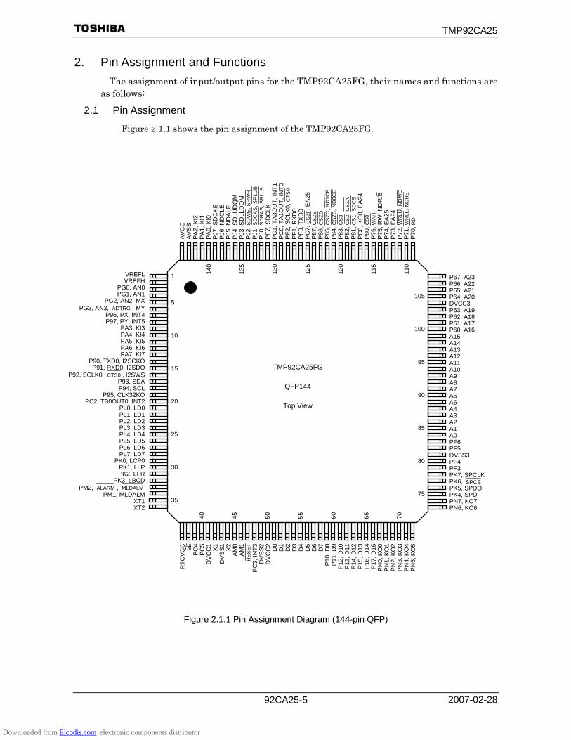
2. Pin Assignment and Functions The assignment of input/output pins for the TMP92CA25FG, their names and functions are
as follows:
2.1 Pin Assignment
Figure 2.1.1 shows the pin assignment of the TMP92CA25FG.
Figure 2.1.1 Pin Assignment Diagram (144-pin QFP)
TMP92CA25FG
QFP144
Top View
P67, A23P66, A22 P65, A21 P64, A20 DVCC3 P63, A19 P62, A18 P61, A17 P60, A16 A15 A14 A13 A12 A11 A10 A9 A8 A7 A6 A5 A4 A3 A2 A1 A0 PF6 PF5 DVSS3 PF4 PF3 PK7, SPCLK PK6, SPCS PK5, SPDO PK4, SPDI PN7, KO7 PN6, KO6
VREFLVREFH
PG0, AN0PG1, AN1
PG2, AN2, MXPG3, AN3, ADTRG , MY
P96, PX, INT4P97, PY, INT5
PA3, KI3PA4, KI4PA5, KI5PA6, KI6PA7, KI7
P90, TXD0, I2SCKOP91, RXD0, I2SDO
P92, SCLK0, 0CTS , I2SWSP93, SDAP94, SCL
P95, CLK32KOPC2, TB0OUT0, INT2
PL0, LD0PL1, LD1PL2, LD2PL3, LD3PL4, LD4PL5, LD5PL6, LD6PL7, LD7
PK0, LCP0PK1, LLPPK2, LFR
PK3, LBCDPM2, ALARM , MLDALM
PM1, MLDALMXT1XT2
RTC
VCC BE
PC
4P
C5
DVC
C1
X1
DV
SS
1 X2
AM0
AM1
RE
SE
TPC
3, IN
T3D
VS
S2
DVC
C2
D0
D1
D2
D3
D4
D5
D6
D7
P10
, D8
P11
, D9
P12
, D10
P13
, D11
P14
, D12
P15
, D13
P16
, D14
P17
, D15
PN
0, K
O0
PN
1, K
O1
PN
2, K
O2
PN
3, K
O3
PN
4, K
O4
PN
5, K
O5
AV
CC
A
VS
S
PA2,
KI2
PA
1, K
I1
PA0,
KI0
P
J7, S
DC
KE
PJ
6, N
DC
LE
PJ5
, ND
ALE
P
J4, S
DLU
DQ
M
PJ3
, SD
LLD
QM
P
J2, S
DW
E, S
RW
R
PJ1
, SD
CAS
, SR
LUB
PJ0
, SD
RAS
, SR
LLB
PF7
, SD
CLK
P
C1,
TA
3OU
T, IN
T1
PC
0, T
A1O
UT,
INT0
P
F2, S
CLK
0, C
TS0
PF1
, RXD
0 P
F0, T
XD0
PC
7, C
SZF
, EA
25
P87
, CS
ZE
P86
, CS
ZD
P85
, CS
ZC, N
D1C
E P
84, C
SZB
, ND
0CE
P83
, CS
3 P
82, C
S2,
CS
ZA
P81
, CS
1, S
DC
S
PC
6, K
O8,
EA
24
P80
, CS
0 P
76, W
AIT
P
75, R
W, N
DR
/B
P74
, EA
25
P73
, EA
24
P72
, WR
LU, N
DW
E P
71, W
RLL
, ND
RE
P70
, RD
1 5 10 15 20 25 30 35
105
100
95
90
85
80
75
140
135
130
125
120
115
110
40
45
50
55
60
65
70
Downloaded from Elcodis.com electronic components distributor
TMP92CA25
2007-02-28 92CA25-6
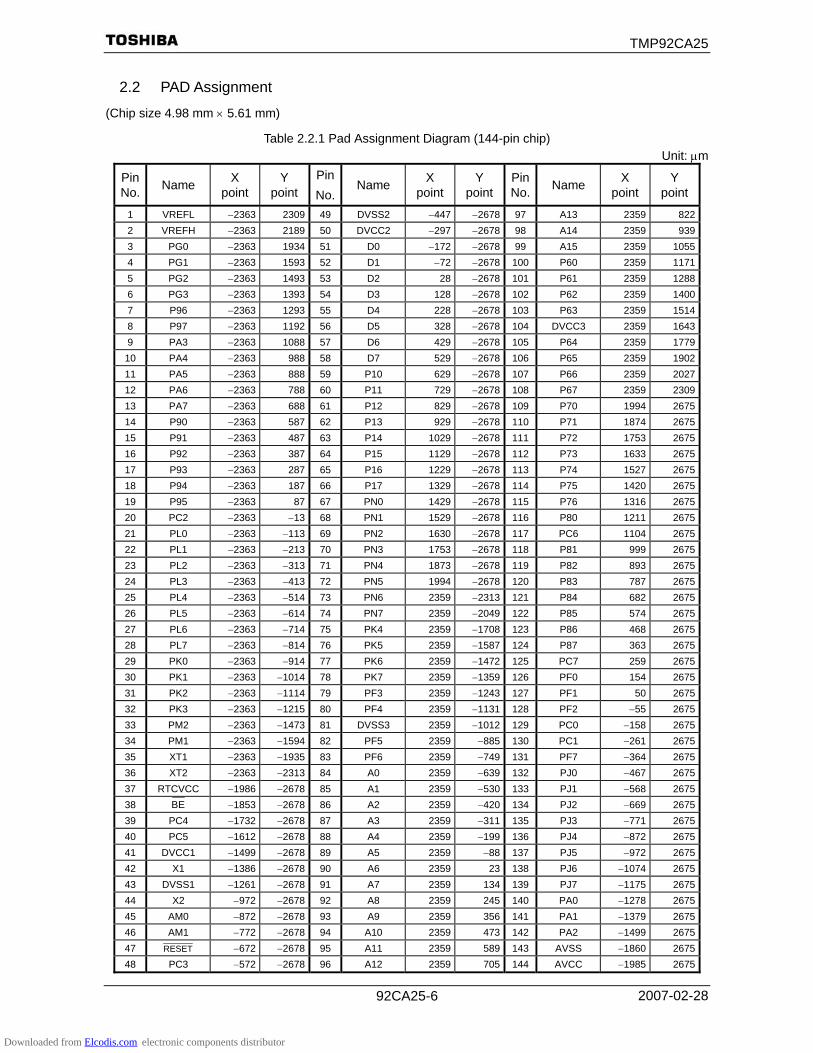
2.2 PAD Assignment
(Chip size 4.98 mm × 5.61 mm)
Table 2.2.1 Pad Assignment Diagram (144-pin chip) Unit: μm
Pin No. Name X
point Y
point Pin No.
Name X point
Y point
PinNo. Name X
point Y
point
1 VREFL −2363 2309 49 DVSS2 −447 −2678 97 A13 2359 8222 VREFH −2363 2189 50 DVCC2 −297 −2678 98 A14 2359 9393 PG0 −2363 1934 51 D0 −172 −2678 99 A15 2359 10554 PG1 −2363 1593 52 D1 −72 −2678 100 P60 2359 11715 PG2 −2363 1493 53 D2 28 −2678 101 P61 2359 12886 PG3 −2363 1393 54 D3 128 −2678 102 P62 2359 14007 P96 −2363 1293 55 D4 228 −2678 103 P63 2359 15148 P97 −2363 1192 56 D5 328 −2678 104 DVCC3 2359 16439 PA3 −2363 1088 57 D6 429 −2678 105 P64 2359 1779
10 PA4 −2363 988 58 D7 529 −2678 106 P65 2359 190211 PA5 −2363 888 59 P10 629 −2678 107 P66 2359 202712 PA6 −2363 788 60 P11 729 −2678 108 P67 2359 230913 PA7 −2363 688 61 P12 829 −2678 109 P70 1994 267514 P90 −2363 587 62 P13 929 −2678 110 P71 1874 267515 P91 −2363 487 63 P14 1029 −2678 111 P72 1753 267516 P92 −2363 387 64 P15 1129 −2678 112 P73 1633 267517 P93 −2363 287 65 P16 1229 −2678 113 P74 1527 267518 P94 −2363 187 66 P17 1329 −2678 114 P75 1420 267519 P95 −2363 87 67 PN0 1429 −2678 115 P76 1316 267520 PC2 −2363 −13 68 PN1 1529 −2678 116 P80 1211 267521 PL0 −2363 −113 69 PN2 1630 −2678 117 PC6 1104 267522 PL1 −2363 −213 70 PN3 1753 −2678 118 P81 999 267523 PL2 −2363 −313 71 PN4 1873 −2678 119 P82 893 267524 PL3 −2363 −413 72 PN5 1994 −2678 120 P83 787 267525 PL4 −2363 −514 73 PN6 2359 −2313 121 P84 682 267526 PL5 −2363 −614 74 PN7 2359 −2049 122 P85 574 267527 PL6 −2363 −714 75 PK4 2359 −1708 123 P86 468 267528 PL7 −2363 −814 76 PK5 2359 −1587 124 P87 363 267529 PK0 −2363 −914 77 PK6 2359 −1472 125 PC7 259 267530 PK1 −2363 −1014 78 PK7 2359 −1359 126 PF0 154 267531 PK2 −2363 −1114 79 PF3 2359 −1243 127 PF1 50 267532 PK3 −2363 −1215 80 PF4 2359 −1131 128 PF2 −55 267533 PM2 −2363 −1473 81 DVSS3 2359 −1012 129 PC0 −158 267534 PM1 −2363 −1594 82 PF5 2359 −885 130 PC1 −261 267535 XT1 −2363 −1935 83 PF6 2359 −749 131 PF7 −364 267536 XT2 −2363 −2313 84 A0 2359 −639 132 PJ0 −467 267537 RTCVCC −1986 −2678 85 A1 2359 −530 133 PJ1 −568 267538 BE −1853 −2678 86 A2 2359 −420 134 PJ2 −669 267539 PC4 −1732 −2678 87 A3 2359 −311 135 PJ3 −771 267540 PC5 −1612 −2678 88 A4 2359 −199 136 PJ4 −872 267541 DVCC1 −1499 −2678 89 A5 2359 −88 137 PJ5 −972 267542 X1 −1386 −2678 90 A6 2359 23 138 PJ6 −1074 267543 DVSS1 −1261 −2678 91 A7 2359 134 139 PJ7 −1175 267544 X2 −972 −2678 92 A8 2359 245 140 PA0 −1278 267545 AM0 −872 −2678 93 A9 2359 356 141 PA1 −1379 267546 AM1 −772 −2678 94 A10 2359 473 142 PA2 −1499 267547 RESET −672 −2678 95 A11 2359 589 143 AVSS −1860 267548 PC3 −572 −2678 96 A12 2359 705 144 AVCC −1985 2675
Downloaded from Elcodis.com electronic components distributor

TMP92CA25
2007-02-28 92CA25-7
2.3 Pin Names and Functions
The following table shows the names and functions of the input/output pins Table 2.3.1 Pin Names and Functions (1/5)
Pin Name Number of
Pins I/O Function
D0 to D7 8 I/O Data: Data bus 0 to 7 P10 to P17 D8 to D15
8 I/O I/O
Port 1: I/O port input or output specifiable in units of bits Data: Data bus 8 to 15
A0 to A7 8 Output Address: Address bus 0 to 7 A8 to A15 8 Output Address: Address bus 8 to 15 P60 to P67 A16 to A23
8 I/O
Output Port 6: I/O port input or output specifiable in units of bits Address: Address bus 16 to 23
P70 RD
1 Output Output
Port70: Output port Read: Outputs strobe signal to read external memory
P71 WRLL NDRE
1 I/O
Output Output
Port 71: I/O port Write: Output strobe signal for writing data on pins D0 to D7 NAND flash read: Outputs strobe signal to read external NAND flash
P72 WRLU NDWE
1 I/O
Output Output
Port 72: I/O port Write: Output strobe signal for writing data on pins D8 to D15 Write Enable for NAND flash
P73 EA24
1 Output Output
Port 73: Output port Extended Address 24
P74 EA25
1 Output Output
Port 74: Output port Extended Address 25
P75 WR/
NDR/ B 1
I/O Output Input
Port 75: I/O port Read/Write: 1 represents read or dummy cycle; 0 represents write cycle NAND flash ready (1)/Busy (0) input
P76 WAIT
1 I/O
Input Port 76: I/O port Wait: Signal used to request CPU bus wait
Downloaded from Elcodis.com electronic components distributor

TMP92CA25
2007-02-28 92CA25-8
Table 2.3.2 Pin Names and Functions (2/5)
Pin Name Number of
Pins I/O Function
P80 0CS 1
Output Output
Port80: Output port Chip select 0: Outputs “low” when address is within specified address area
P81 1CS
SDCS 1
Output Output Output
Port81: Output port Chip select 1: Outputs “low” when address is within specified address area Chip select for SDRAM: Outputs “0” when address is within SDRAM address area
P82 2CS
CSZA 1
Output Output Output
Port82: Output port Chip select 2: Outputs “Low” when address is within specified address area Expand chip select: ZA: Outputs “0” when address is within specified address area
P83 3CS 1
Output Output
Port83: Output port Chip select 3: Outputs “low” when address is within specified address area
P84 CSZB
CE0ND 1
Output Output Output
Port84: Output port Expand chip select: ZB: Outputs “0” when address is within specified address area Chip select for NAND flash 0: Outputs “0” when NAND flash 0 is enabled
P85 CSZC
CE1ND 1
Output Output Output
Port85: Output port Expand chip select: ZC: Outputs “0” when address is within specified address area Chip select for NAND flash 1: Outputs “0” when NAND flash 1 is enabled
P86 CSZD 1
Output Output
Port86: Output port Expand chip select: ZD: outputs “0” when address is within specified address area
P87 CSZE 1
Output Output
Port87: Output port Expand chip select: ZE: Outputs “0” when address is within specified address area
P90 TXD0 I2SCKO
1 I/O
Output Output
Port90: I/O port Serial 0 send data: Open-drain output programmable I2S clock output
P91 RXD0 I2SDO
1 I/O
Input Output
Port91: I/O port (Schmitt-input) Serial 0 receive data I2S data output
P92 SCLK0
0CTS I2SWS
1
I/O I/O
Input Output
Port92: I/O port (Schmitt-input) Serial 0 clock I/O Serial 0 data send enable (Clear to send) I2S word select output
P93 SDA
1 I/O I/O
Port 93: I/O port I2C data I/O
P94 SCL
1 I/O I/O
Port 94: I/O port I2C clock I/O
P95 CLK32KO
1 Output Output
Port95: Output port Output fs (32.768 kHz) clock
P96 INT4 PX
1 Input Input
Output
Port 96: Input port (Schmitt-input) Interrupt request pin4: Interrupt request with programmable rising/falling edge X-Plus: Pin connectted to X+ for touch screen panel
P97 INT5 PY
1 Input Input
Output
Port 97: Input port (Schmitt-input) Interrupt request pin5: Interrupt request with programmable rising/falling edge Y-Plus: Pin connectted to Y+ for touch screen panel
PA0 to PA7 KI0 to KI7
8 Input Input
Port: A0 to A7 port: Pin used to input ports (Schmitt input, with pull-up resistor) Key input 0 to 7: Pin used for key-on wakeup 0 to 7
Downloaded from Elcodis.com electronic components distributor

TMP92CA25
2007-02-28 92CA25-9
Table 2.3.3 Pin Names and Functions (3/5)
Pin Name Number of Pins I/O Function
PC0 INT0 TA1OUT
1 I/O
Input Output
Port C0: I/O port (Schmitt-input) Interrupt request pin 0: Interrupt request pin with programmable level/rising/falling edge 8-bit timer 1 output: Timer 1 output
PC1 INT1 TA3OUT
1 I/O
Input Output
Port C1: I/O port (Schmitt-input) Interrupt request pin 1: Interrupt request pin with programmable rising/falling edge 8-bit timer 3 output: Timer 3 output
PC2 INT2 TB0OUT0
1 I/O
Input Output
Port C2: I/O port (Schmitt-input) Interrupt request pin 2: Interrupt request pin with programmable rising/falling edge Timer B0 output
PC3 INT3
1 I/O
Input Port C3: I/O port (Schmitt-input) Interrupt request pin 3: Interrupt request pin with programmable rising/falling edge
PC4 to PC5 2 I/O Port C4 to C5: U/O port PC6 KO8 EA24
1 I/O
Output Output
Port C6: I/O port Key Output 8: Pin used of key-scan strobe (Open-drain output programmable) Extended Address 24
PC7 CSZF EA25
1 I/O
Output Output
Port C7: I/O port Expand chip select: ZF: Outputs “0” when address is within specified address area Extended Address 25
PF0 TXD0
1 I/O
Output Port F0: I/O port (Schmitt-input) Serial 0 send data: Open-drain output programmable
PF1 RXD0
1 I/O
Input Port F1: I/O port (Schmitt-input) Serial 0 receive data
PF2 SCLK0
0CTS 1
I/O I/O
Input
Port F2: I/O port (Schmitt-input) Serial 0 clock I/O Serial 0 data send enable (Clear to send)
PF7 SDCLK
1 Output Output
Port F7: Output port Clock for SDRAM (When SDRAM is not used, SDCLK can be used as system clock)
PG0 to PG1 AN0 to AN1
2 Input Input
Port G0 to G1 port: Pin used to input ports Analog input 0 to 1: Pin used to Input to AD conveter
PG2 AN2 MX
1 Input Input
Output
Port G2 port: Pin used to input ports Analog input 2: Pin used to Input to AD conveter X-Minus: Pin connectted to X− for touch screen panel
PG3 AN3 MY ADTRG
1
Input Input
Output Intput
Port G3 port: Pin used to input ports Analog input 3: Pin used to input to AD conveter Y-Minus: Pin connectted to Y− for touch screen panel AD trigger: Signal used to request AD start
Downloaded from Elcodis.com electronic components distributor

TMP92CA25
2007-02-28 92CA25-10
Table 2.3.4 Pin Names and Functions (4/5)
Pin Name Number of Pins I/O Function
PJ0 SDRAS SRLLB
1 Output Output Output
Port J0: Output port Row address strobe for SDRAM Data enable for SRAM on pins D0 to D7
PJ1 SDCAS SRLUB
1 Output Output Output
Port J1: Output port Column address strobe for SDRAM Data enable for SRAM on pins D8 to D15
PJ2 SDWE SRWR
1 Output Output Output
Port J2: Output port Write enable for SDRAM Write for SRAM: Strobe signal for writing data
PJ3 SDLLDQM
1 Output Output
Port J3: Output port Data enable for SDRAM on pins D0 to D7
PJ4 SDLUDQM
1 Output Output
Port J4: Output port Data enable for SDRAM on pins D8 to D15
PJ5 NDALE
1 I/O
Output Port J5: I/O port Address latch enable for NAND flash
PJ6 NDCLE
1 I/O
Output Port J6: I/O port Command latch enable for NAND flash
PJ7 SDCKE
1 Output Output
Port J7: Output port Clock enable for SDRAM
PK0 LCP0
1 Output Output
Port K0: Output port LCD driver output pin
PK1 LLP
1 Output Output
Port K1: Output port LCD driver output pin
PK2 LFR
1 Output Output
Port K2: Output port LCD driver output pin
PK3 LBCD
1 Output Output
Port K3: Output port LCD driver output pin
PK4 SPDI
1 I/O
Input Port K4: I/O port Data input pin for SD card
PK5 SPDO
1 I/O
Output Port K5: I/O port Data output pin for SD card
PK6 SPCS
1 I/O
Output Port K6: I/O port Chip select pin for SD card
PK7 SPCLK
1 I/O
Output Port K7: I/O port Clock output pin for SD card
PL0 to PL3 LD0 to LD3
4 Output Output
Port L0 to L3: Output port Data bus for LCD driver
PL4 to PL5 LD4 to LD5
2 I/O
Output Port L4 to L5: I/O port Data bus for LCD driver
PL6 LD6 BUSRQ
1 I/O Output Input
Port L6: I/O port Data bus for LCD driver Bus request: request pin that set external memory bus to high-impedance (for External DMAC)
PL7 LD7 BUSAK
1 I/O Output Output
Port L7: I/O port Data bus for LCD driver Bus acknowledge: this pin show that external memory bus pin is set to high-impedance by
receiving BUSRQ (for External DMAC)
Downloaded from Elcodis.com electronic components distributor

TMP92CA25
2007-02-28 92CA25-11
Table 2.3.5 Pin Names and Functions (5/5)
Pin Name Number of Pins I/O Function
PM1 MLDALM
1 Output Output
Port M1: Output port Melody/alarm output pin
PM2 ALARM MLDALM
1 Output Output Output
Port M2: Output port RTC alarm output pin Melody/alarm output pin (inverted)
PN0 to PN7 KO0 to KO7
8 I/O Output
Port N0 to N7: I/O port Key out pin (Open-drain setting )
AM0, AM1 2 Input
Operation mode: Fix to AM1 = “0”, AM0 = “1” for 16-bit external bus starting Fix to AM1 = “1”, AM0 = “0” for 32-bit external bus starting Fix to AM1 = “1”, AM0 = “1” Prohibit setting Fix to AM1 = “0”, AM0 = “0” Prohibit setting
X1/X2 2 I/O High-frequency oscillator connection pins XT1/XT2 2 I/O Low-frequency oscillator connection pins RESET 1 Input Reset: Initializes TMP92CA25 (with pull-up resistor, Schmitt input) VREFH 1 Input Pin for reference voltage input to AD converter (H) VREFL 1 Input Pin for reference voltage input to AD converter (L) RTCVCC 1 − Power supply pin for RTC BE 1 Input Back up enable pin: When power off DVCC and AVSS during RTC is operating, set to “L” level
beforehand. Usually, this pin used to “H” level. (Schmitt input) AVCC 1 − Power supply pin for AD converter AVSS 1 − GND pin for AD converter (0 V) DVCC 3 − Power supply pins (All DVCC pins should be connected to the power supply pin) DVSS 3 − GND pins (0 V) (All DVSS pins should be connected to GND (0 V))
Downloaded from Elcodis.com electronic components distributor

TMP92CA25
2007-02-28 92CA25-12
3. Operation This section describes the basic components, functions and operation of the TMP92CA25.
3.1 CPU
The TMP92CA25 contains an advanced high-speed 32-bit CPU (TLCS-900/H1 CPU)
3.1.1 CPU Outline
The TLCS-900/H1 CPU is a high-speed, high-performance CPU based on the TLCS-900/L1 CPU. The TLCS-900/H1 CPU has an expanded 32-bit internal data bus to process instructions more quickly.
The following is an outline of the CPU:
Table 3.1.1 TMP92CA25 Outline
Parameter TMP92CA25
Width of CPU address bus 24 bits
Width of CPU data bus 32 bits
Internal operating frequency Max 20 MHz
Minimum bus cycle 1-clock access (50 ns at fSYS = 20MHz)
Internal RAM 32-bit 1-clock access
8-bit 2-clock accessINTC, SDRAMC,
MEMC, NDFC, TSI, PORT
16-bit 2-clock access
I2S, SPIC, LCDC Internal I/O
8-bit 5∼6-clock access
TMRA, TMRB, SIO, RTC, MLD/ALM, SBI,
CGEAR, ADC
External SRAM, Masked ROM 8- or 16-bit 2-clock access
(waits can be inserted)
External SDRAM 16-bit 1-clock access
External NAND flash 8-bit 4-clock access
(waits can be inserted)
Minimum instruction
execution cycle 1-clock (50 ns at fSYS = 20MHz)
Conditional jump 2-clock (100 ns at fSYS = 20MHz)
Instruction queue buffer 12 bytes
Instruction set Compatible with TLCS-900/L1
(LDX instruction is deleted)
CPU mode Maximum mode only
Micro DMA 8 channels
Downloaded from Elcodis.com electronic components distributor

TMP92CA25
2007-02-28 92CA25-13
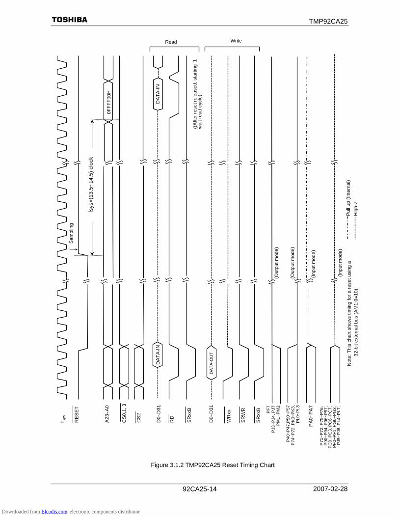
3.1.2 Reset Operation
When resetting the TMP92CA25, ensure that the power supply voltage is within the operating voltage range, and that the internal high-frequency oscillator has stabilized. Then hold the RESET input low for at least 20 system clocks (16 µs at fc = 40 MHz).
At reset, since the clock doubler (PLL) is bypassed and the clock-gear is set to 1/16, the system clock operates at 1.25 MHz (fc = 40 MHz).
When the reset has been accepted, the CPU performs the following: • Sets the program counter (PC) as follows in accordance with the reset vector stored
at address FFFF00H to FFFF02H: PC<7:0> ← data in location FFFF00H PC<15:8> ← data in location FFFF01H PC<23:16> ← data in location FFFF02H
• Sets the stack pointer (XSP) to 00000000H. • Sets bits <IFF2:0> of the status register (SR) to 111 (thereby setting the interrupt
level mask register to level 7). • Clears bits <RFP1:0> of the status register to 00 (there by selecting register bank
0). When the reset is released, the CPU starts executing instructions according to the
program counter settings. CPU internal registers not mentioned above do not change when the reset is released.
When the reset is accepted, the CPU sets internal I/O, ports and other pins as follows. • Initializes the internal I/O registers as shown in the “Special Function Register”
table in section 5. • Sets the port pins, including the pins that also act as internal I/O, to
general-purpose input or output port mode. Internal reset is released as soon as external reset is released. Memory controller operation cannot be ensured until the power supply becomes stable
after power-on reset. External RAM data provided before turning on the TMP92CA25 may be corrupted because the control signals are unstable until the power supply becomes stable after power on reset.
Figure 3.1.1 Power on Reset Timing Example
High-frequency oscillation stabilized time+20 system clock
0 s (Min)
VCC (3.3 V)
RESET
Downloaded from Elcodis.com electronic components distributor
TMP92CA25
2007-02-28 92CA25-14
Figure 3.1.2 TMP92CA25 Reset Timing Chart
Read Write
f sys
A23
∼A0
DA
TA-IN
D
0∼D
31
D0∼
D31
((A
fter r
eset
rele
ased
, sta
rting
1w
ait r
ead
cycl
e)
Sam
plin
g R
ES
ET
RD
WR
xx
SR
WR
0FFF
F00H
DA
TA-IN
DA
TA-O
UT
CS
0,1,
3
CS
2
SR
xxB
SR
xxB
fsys
×(13
.5~1
4.5)
clo
ck
Pul
l up
(Inte
rnal
) H
igh-
Z
(Inpu
t mod
e)
PA
0~P
A7
(Out
put m
ode)
PF7
PJ3
~PJ4
, PJ7
PM1~
PM2
(Inpu
t mod
e)
P71
~P72
, P75
~P76
,P
90~P
94, P
96~P
97,
PC
0~PC
3, P
C6~
PC7,
PF0
~PF1
, PG
0~PG
3,P
J5~P
J6, P
L4~P
L7,
(Out
put m
ode)
P
40~P
47,P
50~P
57P
74~P
72, P
K0~
PK3
,P
L0~P
L3
Not
e: T
his
char
t sho
ws
timin
g fo
r a re
set u
sing
a
32-b
it ex
tern
al b
us (A
M1:
0=10
).
Downloaded from Elcodis.com electronic components distributor

TMP92CA25
2007-02-28 92CA25-15
3.1.3 Setting of AM0 and AM1
Set AM1 and AM0 pins as shown in Table 3.1.2 according to system usage.
Table 3.1.2 Operation Mode Setup Table Mode Setup Input Pin
Operation Mode RESET AM1 AM0
16-bit external bus starting (MULTI 16 mode)
0 1
8-bit external bus starting (MULTI 8 mode)
1 0
Prohibit setting 1 1
Reserve (Toshiba test mode)
0 0
Downloaded from Elcodis.com electronic components distributor

TMP92CA25
2007-02-28 92CA25-16
3.2 Memory Map
Figure 3.2.1 is a memory map of the TMP92CA25.
Figure 3.2.1 Memory Map
Note 1: The Provisional emulator control area, mapped F00000H to F0FFFFH after reset, is for emulator use and so is not available.
When emulator WR signal and RD signal are asserted, this area is accessed. Ensure external memory is used.
Note 2: Do not use the last 16-byte area (FFFFF0H to FFFFFFH). This area is reserved for an emulator.
External memory
External memory
Vector table (256 bytes)
Internal I/O (8 Kbytes)
Internal RAM (10 Kbytes)
Direct area (n)
64-Kbyte area(nn)
16-Mbyte area (R) (−R) (R+) (R + R8/16) (R + d8/16) (nnn)
000000H
000100H
001D00H002000H
004800H
F00000H
F10000H
FFFF00H
FFFFFFH
( = Internal area)
Provisional emulator control (64 Kbytes)
010000H
(Note 1)
(Note 2)
Downloaded from Elcodis.com electronic components distributor

TMP92CA25
2007-02-28 92CA25-17
3.3 Clock Function and Stand-by Function
The TMP92CA25 contains (1) clock gear, (2) clock doubler (PLL), (3) stand-by controller and (4) noise reduction circuits. They are used for low power, low noise systems.
This chapter is organized as follows: 3.3.1 Block diagram of system clock 3.3.2 SFR 3.3.3 System clock controller 3.3.4 Clock doubler (PLL) 3.3.5 Noise reduction circuits 3.3.6 Stand-by controller
Downloaded from Elcodis.com electronic components distributor

TMP92CA25
2007-02-28 92CA25-18
The clock operating modes are as follows: (a) single clock mode (X1, X2 pins only), (b) dual clock mode (X1, X2, XT1 and XT2 pins) and (c) triple clock mode (X1, X2, XT1 and XT2 pins and PLL).
Figure 3.3.1 shows a transition figure.
Reset (fOSCH/32)
Release resetInstructionInterrupt STOP mode
(Stops all circuits) NORMAL mode
(fOSCH/gear value/2)
IDLE2 mode (I/O operate)
IDLE1 mode (Operate only oscillator)
(a) Single clock mode transition figure
(b) Dual clock mode transition figure
SLOW mode (fs/2)
Reset (fOSCH/32)
Release reset
NORMAL mode (fOSCH/gear value/2)
IDLE2 mode (I/O operate)
IDLE1 mode (Operate only oscillator)
IDLE2 mode (I/O operate)
IDLE1 mode (Operate only oscillator)
Instruction
Instruction Interrupt
Interrupt
Instruction
Instruction Interrupt
Interrupt
Instruction
Instruction Interrupt
Interrupt
InstructionInterrupt STOP mode
(Stops all circuits)
InstructionInterrupt STOP mode
(Stops all circuits)
Using PLL
Note
Reset (fOSCH/32)
Release reset
NORMAL mode (fOSCH/gear value/2)
IDLE2 mode (I/O operate)
IDLE1 mode (Operate only oscillator)
STOP mode (Stops all circuits)
SLOW mode (fs/2)
NORMAL mode (4 × fOSCH/gear
value/2)
IDLE2 mode (I/O operate)
IDLE1 mode (Operate oscillator and PLL)
IDLE2 mode (I/O operate)
IDLE1 mode (Operate only oscillator)
(c) Triple clock mode transition figure
Instruction
Instruction Interrupt
Interrupt
Instruction Instruction
InstructionInterrupt
Note
Instruction
Instruction Interrupt
Instruction
Instruction
Interrupt
Interrupt
Interrupt
Interrupt
Instruction
Instruction
Instruction Interrupt
Note 1: It is not possible to control PLL in SLOW mode when shifting from SLOW mode to NORMAL mode with use of PLL.
(PLL start up/stop/change write to PLLCR0<PLLON>, PLLCR1<FCSEL> register)
Note 2: When shifting from NORMAL mode with use of PLL to NORMAL mode, execute the following setting in the same order.
1) Change CPU clock (PLLCR0<FCSEL> ← “0”)
2) Stop PLL circuit (PLLCR1<PLLON> ← “0”)
Note 3: It is not possible to shift from NORMAL mode with use of PLL to STOP mode directly.
NORMAL mode should be set once before shifting to STOP mode. (Sstop the high-frequency oscillator after stopping
PLL.)
Figure 3.3.1 System Clock Block Diagram
The clock frequency input from the X1 and X2 pins is called fc and the clock frequency input from the XT1 and XT2 pins is called fs. The clock frequency selected by SYSCR1<SYSCK> is called the clock fFPH. The system clock fSYS is defined as the divided clock of fFPH, and one cycle of fSYS is defined as one state.
Downloaded from Elcodis.com electronic components distributor

TMP92CA25
2007-02-28 92CA25-19
3.3.1 Block Diagram of System Clock
Figure 3.3.2 Block Diagram of System Clock
TMRA0 to 3, TMRB0
fSYS CPU
RAM, ROM
I2S
Interrupt controller
I/O ports
PrescalerφT0
SIO0 to SIO1
RTC
fs
Prescaler
MLD/ALM
SDRAMC
fIO
Clock-gear
SYSCR1<SYSCK> Selector
fs
fOSCH
Low-frequency oscillator
XT1
XT2
SYSCR0<XTEN >
Warm-up timer (High/low-frequency oscillator)
SYSCR0<WUEF> SYSCR2<WUPTM1:0>
X1
X2
Clock doubler (PLL)
fPLL = fOSCH × 4
÷2 ÷16÷4
fc/16fc/8
fc/4fc/2
fc
PLLCR0<FCSEL>
SYSCR1<GEAR2:0>
÷4 ÷8 fFPH
fSYS÷2
φT0
fs
φT
SYSCR0<XEN >
High-frequency oscillator
÷8
÷2 fIO
LCDC
Memory controller
NAND flash controller
TSI
Lock up timer (PLL)
PLLCR1<PLLON>, PLLCR0<LUPFG>
ADC
WDT
SPIC I2C bus Prescaler
Downloaded from Elcodis.com electronic components distributor

TMP92CA25
2007-02-28 92CA25-20
3.3.2 SFR
7 6 5 4 3 2 1 0 Bit symbol XEN XTEN WUEF
Read/Write R/W R/W After reset 1 1 0 Function High-
frequency oscillator (fc) 0: Stop 1: Oscillation
Low- frequency oscillator (fs) 0: Stop 1: Oscillation
Warm-up timer 0: Write
don’t care
1: Write start timer
0: Read end warm-up
1: Read do not end warm-up
7 6 5 4 3 2 1 0 Bit symbol SYSCK GEAR2 GEAR1 GEAR0
Read/Write R/W After reset 0 1 0 0 Function Select
system clock0: fc 1: fs
Select gear value of high-frequency (fc)000: fc 001: fc/2 010: fc/4 011: fc/8 100: fc/16 101: (Reserved) 110: (Reserved) 111: (Reserved)
7 6 5 4 3 2 1 0 Bit symbol − WUPTM1 WUPTM0 HALTM1 HALTM0
Read/Write R/W R/W After reset 0 1 0 1 1 Function Always
write “0” Warm-up timer
00: Reserved 01: 28/input frequency 10: 214/input frequency 11: 216/input frequency
HALT mode 00: Reserved 01: STOP mode 10: IDLE1 mode 11: IDLE2 mode
Note 1: The unassigned registers, SYSCR0<bit5:3>, SYSCR0<bit1:0>, SYSCR1<bit7:4>, and SYSCR2<bit6, bit1:0> are read as undefined value.
Note 2: Low-frequency oscillator is enabled on reset.
Figure 3.3.3 SFR for System Clock
SYSCR0 (10E0H)
SYSCR1 (10E1H)
SYSCR2 (10E2H)
Downloaded from Elcodis.com electronic components distributor

TMP92CA25
2007-02-28 92CA25-21
7 6 5 4 3 2 1 0
Bit symbol PROTECT EXTIN DRVOSCH DRVOSCLRead/Write R R/W After reset 0 0 1 1 Function Protect flag
0: OFF 1: ON
1: External clock
fc oscillator driver ability
1: Normal
0: Weak
fs oscillator driver ability
1: Normal
0: Weak
Bit symbol
Read/Write After reset Function
Bit symbol
Read/Write After reset Function
Switch the protect ON/OFF by writing the following to 1st-KEY, 2nd-KEY 1st-KEY: write in sequence EMCCR1 = 5AH, EMCCR2 = A5H 2nd-KEY: write in sequence EMCCR1 = A5H, EMCCR2 = 5AH
Note: When restarting the oscillator from the stop oscillation state (e.g. restarting the oscillator in STOP mode), set
EMCCR0<DRVOSCH>, <DRVOSCL> = “1”.
Figure 3.3.4 SFR for System Clock
EMCCR0 (10E3H)
EMCCR1 (10E4H)
EMCCR2 (10E5H)
Downloaded from Elcodis.com electronic components distributor

TMP92CA25
2007-02-28 92CA25-22
7 6 5 4 3 2 1 0
Bit symbol FCSEL LUPFG Read/Write R/W R After reset 0 0 Function Select fc
clock 0: fOSCH 1: fPLL
Lock up timer status flag0: Not end1: End
Note: Ensure that the logic of PLLCR0<LUPFG> is different from 900/L1’s DFM.
7 6 5 4 3 2 1 0 Bit symbol PLLON
Read/Write R/W After reset 0 Function Control
on/off 0: OFF 1: ON
Figure 3.3.5 SFR for PLL
7 6 5 4 3 2 1 0 Bit symbol Px7D Px6D Px5D Px4D Px3D Px2D Px1D Px0D
Read/Write R/W After reset 1 1 1 1 1 1 1 1 Function Output/input buffer drive-register for stand-by mode
(Purpose and use)
This register is used to set each pin status at stand-by mode.
All ports have registers of the format shown above. (“x” indicates the port name.)
For each register, refer to “3.5 Function of ports”.
Before “Halt” instruction is executed, set each register according to the expected pin-status. They will be effective
after the CPU has executed the “Halt” instruction.
This is the case regardless of stand-by mode (IDLE2, IDLE1 or STOP).
The output/input buffer control table is shown below.
OE PxnD Output Buffer Input Buffer
0 0 OFF OFF 0 1 OFF ON 1 0 OFF OFF 1 1 ON OFF
Note 1: OE denotes an output enable signal before stand-by mode.
Basically, PxCR is used as OE.
Note 2: “n” in PxnD denotes the bit number of PORTx.
Figure 3.3.6 SFR for Drive Register
PLLCR0 (10E8H)
PLLCR1 (10E9H)
PxDR (xxxxH)
Downloaded from Elcodis.com electronic components distributor

TMP92CA25
2007-02-28 92CA25-23
3.3.3 System Clock Controller
The system clock controller generates the system clock signal (fSYS) for the CPU core and internal I/O. It contains two oscillation circuits and a clock gear circuit for high-frequency (fc) operation. The register SYSCR1<SYSCK> changes the system clock to either fc or fs, SYSCR0<XEN> and SYSCR0<XTEN> control enabling and disabling of each oscillator, and SYSCR1<GEAR2:0> sets the high-frequency clock gear to either 1, 2, 4, 8 or 16 (fc, fc/2, fc/4, fc/8 or fc/16). These functions can reduce the power consumption of the equipment in which the device is installed.
The combination of settings <XEN> = 1, <SYSCK> = 0 and <GEAR2:0> = 100 will cause the system clock (fSYS) to be set to fc/32 (fc/16 × 1/2) after reset.
For example, fSYS is set to 1.25 MHz when the 40 MHz oscillator is connected to the X1 and X2 pins.
(1) Switching from normal mode to slow mode
When the resonator is connected to the X1 and X2 pins, or to the XT1 and XT2 pins, the warm-up timer can be used to change the operation frequency after stable oscillation has been attained.
The warm-up time can be selected using SYSCR2<WUPTM1:0>. This warm-up timer can be programmed to start and stop as shown in the following
examples 1 and 2. Table 3.3.1 shows the warm-up time.
Note 1: When using an oscillator (other than a resonator) with stable oscillation, a warm-up timer is not needed.
Note 2: The warm-up timer is operated by an oscillation clock. Hence, there may be some variation in warm-up time.
Table 3.3.1 Warm-up Times at fOSCH = 40 MHz, fs = 32.768 kHz
Warm-up Time SYSCR2
<WUPTM1:0>
Change to Normal Mode
Change to Slow Mode
01 (28/frequency) 6.4 (μs) 7.8 (ms) 10 (214/frequency) 409.6 (μs) 500 (ms) 11 (216/frequency) 1.638 (ms) 2000 (ms)
Downloaded from Elcodis.com electronic components distributor
TMP92CA25
2007-02-28 92CA25-24
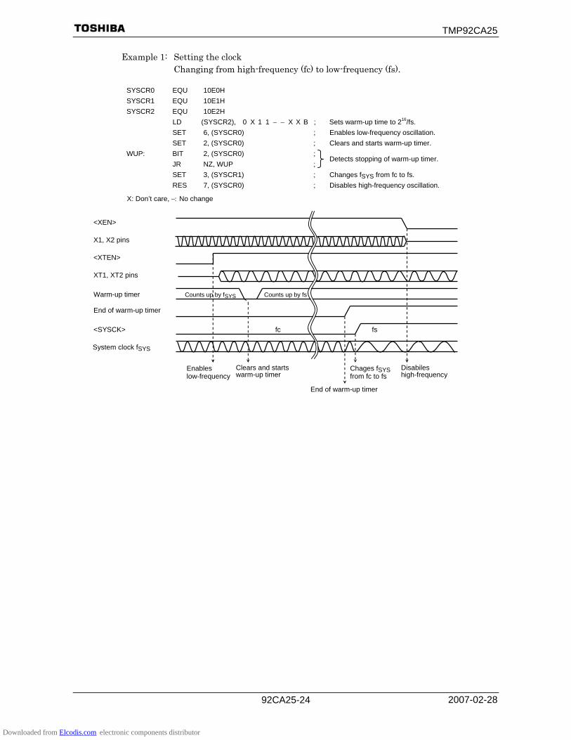
Example 1: Setting the clock Changing from high-frequency (fc) to low-frequency (fs).
SYSCR0 EQU 10E0H SYSCR1 EQU 10E1H SYSCR2 EQU 10E2H
LD (SYSCR2), 0 X 1 1 − − X X B ; Sets warm-up time to 216/fs. SET 6, (SYSCR0) ; Enables low-frequency oscillation. SET 2, (SYSCR0) ; Clears and starts warm-up timer. WUP: BIT 2, (SYSCR0) ; JR NZ, WUP ;
Detects stopping of warm-up timer.
SET 3, (SYSCR1) ; Changes fSYS from fc to fs. RES 7, (SYSCR0) ; Disables high-frequency oscillation.
X: Don’t care, −: No change
Enables low-frequency
Clears and startswarm-up timer
Chages fSYSfrom fc to fs
End of warm-up timer
Disabiles high-frequency
fc
<XEN>
X1, X2 pins
<XTEN>
XT1, XT2 pins
Warm-up timer
<SYSCK>
System clock fSYS
End of warm-up timer
fs
Counts up by fSYS Counts up by fs
Downloaded from Elcodis.com electronic components distributor

TMP92CA25
2007-02-28 92CA25-25
Example 2: Setting the clock Changing from low-frequency (fs) to high-frequency (fc).
SYSCR0 EQU 10E0H SYSCR1 EQU 10E1H SYSCR2 EQU 10E2H
LD (SYSCR2), 0 X 1 0 − − X X B ; Sets warm-up time to 214/fc. SET 7, (SYSCR0) ; Enables high-frequency oscillation. SET 2, (SYSCR0) ; Clears and starts warm-up timer. WUP: BIT 2, (SYSCR0) ; JR NZ, WUP ;
Detects stopping of warm-up timer.
RES 3, (SYSCR1) ; Changes fSYS from fs to fc. RES 6, (SYSCR0) ; Disables low-frequency oscillation.
X: Don’t care, −: No change
Counts up by fSYS Counts up by fc
Disables low-frequency
Enables high-frequency
Clears and starts warm-up timer
Changes fSYSfrom fs to fc
End of warm-up timer
<XEN>
X1, X2 pins
<XTEN>
XT1, XT2 pins
Warm-up timer
<SYSCK>
System Clock fSYS
End of warm-up timer
fcfs
Downloaded from Elcodis.com electronic components distributor

TMP92CA25
2007-02-28 92CA25-26
(2) Clock gear controller fFPH is set according to the contents of the clock gear select register
SYSCR1<GEAR2:0> to either fc, fc/2, fc/4, fc/8 or fc/16. Using the clock gear to select a lower value of fFPH reduces power consumption.
Example 3: Changing to a high-frequency gear
SYSCR1 EQU 10E1H
LD (SYSCR1), XXXX0000B ; Changes fSYS to fc/2. LD (DUMMY), 00H ; Dummy instruction
X: Don’t care
(High-speed clock gear changing) To change the clock gear, write the register value to the SYSCR1<GEAR2:0>
register.It is necessary for the warm-up time to elapse before the change occurs after writing the register value.
There is the possibility that the instruction following the clock gear changing instruction is executed by the clock gear before changing.To execute the instruction following the clock gear switching instruction by the clock gear after changing, input the dummy instruction as follows (instruction to execute the write cycle).
Example:
SYSCR1 EQU 10E1H LD (SYSCR1), XXXX0001B ; Changes fSYS to fc/4. LD (DUMMY), 00H ; Dummy instruction Instruction to be executed after clock gear has changed
Downloaded from Elcodis.com electronic components distributor
TMP92CA25
2007-02-28 92CA25-27
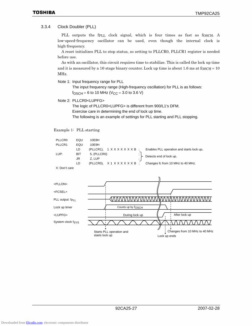
3.3.4 Clock Doubler (PLL)
PLL outputs the fPLL clock signal, which is four times as fast as fOSCH. A low-speed-frequency oscillator can be used, even though the internal clock is high-frequency.
A reset initializes PLL to stop status, so setting to PLLCR0, PLLCR1 register is needed before use.
As with an oscillator, this circuit requires time to stabilize. This is called the lock up time and it is measured by a 16-stage binary counter. Lock up time is about 1.6 ms at fOSCH = 10 MHz.
Note 1: Input frequency range for PLL The input frequency range (High-frequency oscillation) for PLL is as follows: fOSCH = 6 to 10 MHz (VCC = 3.0 to 3.6 V)
Note 2: PLLCR0<LUPFG> The logic of PLLCR0<LUPFG> is different from 900/L1’s DFM. Exercise care in determining the end of lock up time. The following is an example of settings for PLL starting and PLL stopping.
Example 1: PLL starting
PLLCR0 EQU 10E8H PLLCR1 EQU 10E9H
LD (PLLCR1), 1 X X X X X X X B ; Enables PLL operation and starts lock up. LUP: BIT 5, (PLLCR0) ; JR Z, LUP ;
Detects end of lock up.
LD (PLLCR0), X 1 X X X X X X B ; Changes fc from 10 MHz to 40 MHz. X: Don’t care
Counts up by fOSCH
Changes from 10 MHz to 40 MHzStarts PLL operation andstarts lock up
<PLLON>
<FCSEL>
PLL output: fPLL
Lock up timer
<LUPFG>
System clock fSYS
After lock up During lock up
Lock up ends
Downloaded from Elcodis.com electronic components distributor
TMP92CA25
2007-02-28 92CA25-28
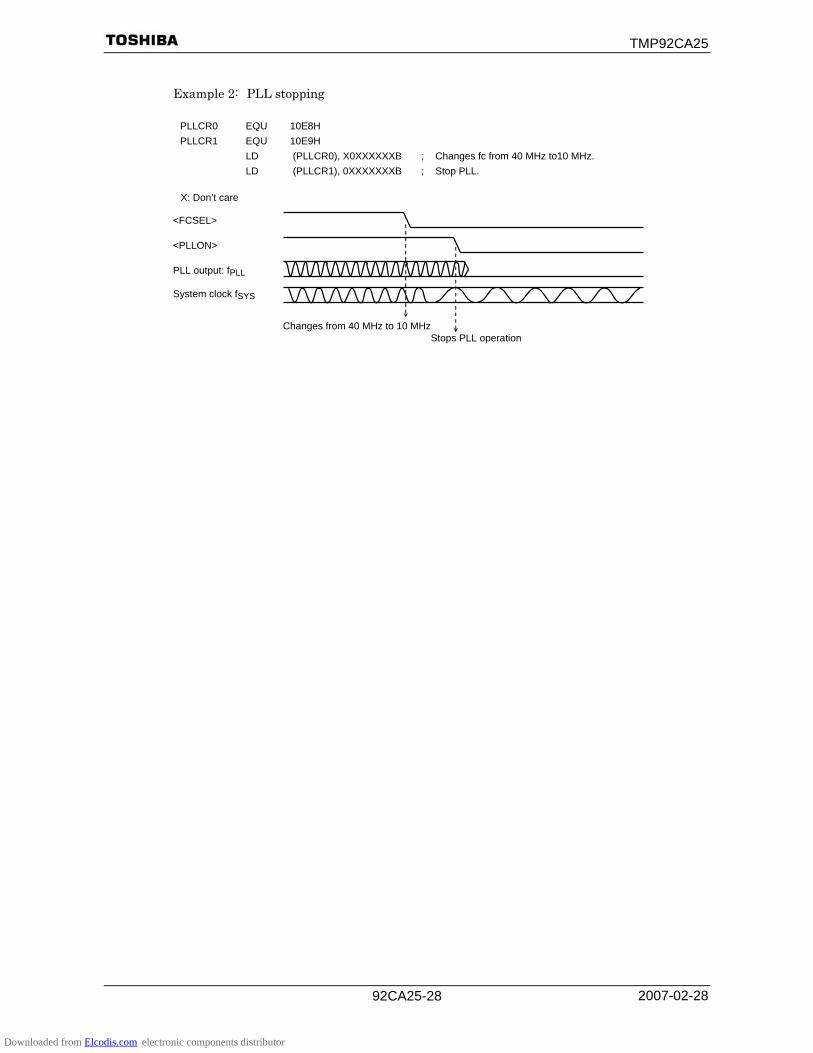
Example 2: PLL stopping
PLLCR0 EQU 10E8H PLLCR1 EQU 10E9H LD (PLLCR0), X0XXXXXXB ; Changes fc from 40 MHz to10 MHz. LD (PLLCR1), 0XXXXXXXB ; Stop PLL.
X: Don’t care
Changes from 40 MHz to 10 MHz
<FCSEL>
<PLLON>
PLL output: fPLL
System clock fSYS
Stops PLL operation
Downloaded from Elcodis.com electronic components distributor

TMP92CA25
2007-02-28 92CA25-29
Limitations on the use of PLL
1. It is not possible to execute PLL enable/disable control in the SLOW mode (fs) (writing to PLLCR0 and PLLCR1). PLL should be controlled in the NORMAL mode.
2. When stopping PLL operation during PLL use, execute the following settings in the
same order. LD (PLLCR0), 00H ; Change the clock fPLL to fOSCH LD (PLLCR1), 00H ; PLL stop
3. When stopping the high-frequency oscillator during PLL use, stop PLL before stopping
the high-frequency oscillator.
Examples of settings are shown below:
(1) Start up/change control (OK) Low-frequency oscillator operation mode (fs) (high-frequency oscillator STOP)
→ High-frequency oscillator start up → High-frequency oscillator operation mode (fOSCH) → PLL start up → PLL use mode (fPLL)
LD (SYSCR0), 1 1 − − − 1 − − B ; High-frequency oscillator start/warm-up start WUP: BIT 2, (SYSCR0) ; JR NZ, WUP ;
Check for warm-up end flag
LD (SYSCR1), − − − − 0 − − − B ; Change the system clock fs to fOSCH LD (PLLCR1), 1 − − − − − − − B ; PLL start-up/lock up start LUP: BIT 5, (PLLCR0) ; JR Z, LUP ;
Check for lock up end flag
LD (PLLCR0), − 1 − − − − − − B ; Change the system clock fOSCH to fPLL
(OK) Low-frequency oscillator operation mode (fs) (high-frequency oscillator Operate) → High-frequency oscillator operation mode (fOSCH) → PLL start up → PLL use mode (fPLL)
LD (SYSCR1), − − − − 0 − − − B ; Change the system clock fs to fOSCH LD (PLLCR1), 1 − − − − − − − B ; PLL start-up/lock up start LUP: BIT 5, (PLLCR0) ; JR Z, LUP ;
Check for lock up end flag
LD (PLLCR0), − 1 − − − − − − B ; Change the system clock fOSCH to fPLL
(Error) Low-frequency oscillator operation mode (fs) (high-frequency oscillator STOP) → High-frequency oscillator start up → PLL start up → PLL use mode (fPLL)
LD (SYSCR0), 1 1 − − − 1 − − B ; High-frequency oscillator start/warm-up start WUP: BIT 2, (SYSCR0) ; JR NZ, WUP ;
Check for warm-up end flag
LD (PLLCR1), 1 − − − − − − − B ; PLL start-up/lock up start LUP: BIT 5, (PLLCR0) ; JR Z, LUP ;
Check for lock up end flag
LD (PLLCR0), − 1 − − − − − − B ; Change the internal clock fOSCH to fPLL LD (SYSCR1), − − − − 0 − − − B ; Change the system clock fs to fPLL
Downloaded from Elcodis.com electronic components distributor
TMP92CA25
2007-02-28 92CA25-30
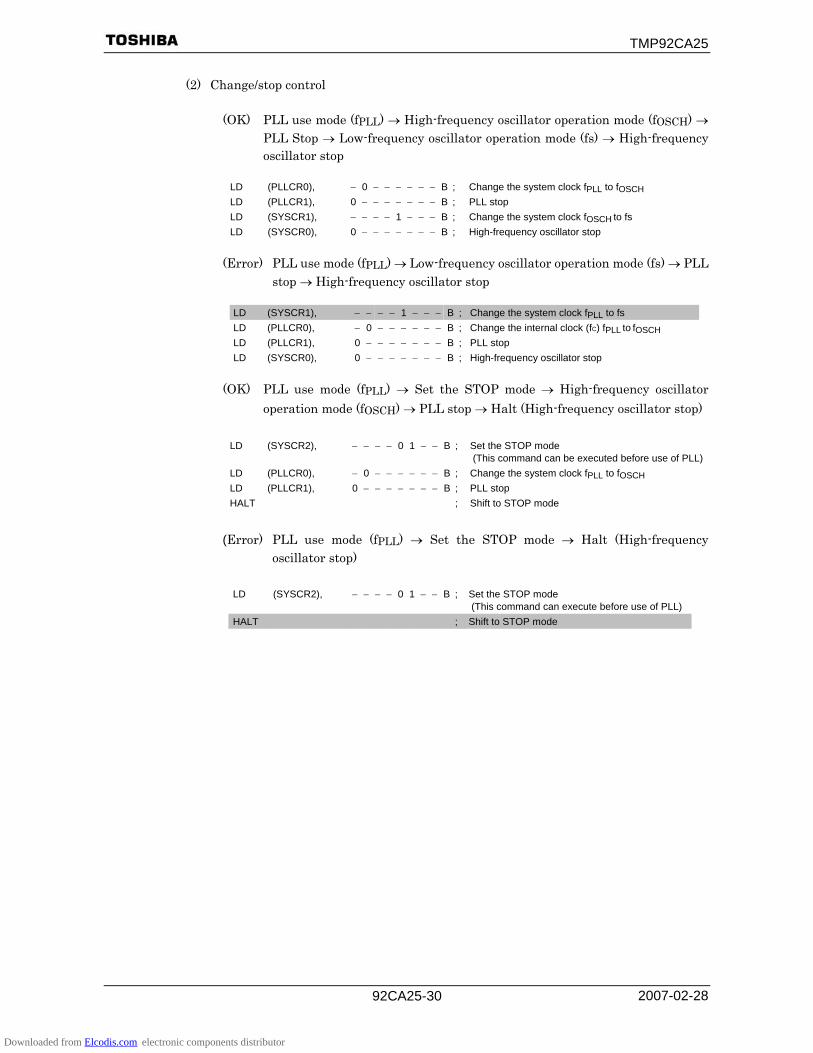
(2) Change/stop control
(OK) PLL use mode (fPLL) → High-frequency oscillator operation mode (fOSCH) → PLL Stop → Low-frequency oscillator operation mode (fs) → High-frequency oscillator stop
LD (PLLCR0), − 0 − − − − − − B ; Change the system clock fPLL to fOSCH LD (PLLCR1), 0 − − − − − − − B ; PLL stop LD (SYSCR1), − − − − 1 − − − B ; Change the system clock fOSCH to fs LD (SYSCR0), 0 − − − − − − − B ; High-frequency oscillator stop
(Error) PLL use mode (fPLL) → Low-frequency oscillator operation mode (fs) → PLL
stop → High-frequency oscillator stop
LD (SYSCR1), − − − − 1 − − − B ; Change the system clock fPLL to fs LD (PLLCR0), − 0 − − − − − − B ; Change the internal clock (fC) fPLL to fOSCH LD (PLLCR1), 0 − − − − − − − B ; PLL stop LD (SYSCR0), 0 − − − − − − − B ; High-frequency oscillator stop
(OK) PLL use mode (fPLL) → Set the STOP mode → High-frequency oscillator
operation mode (fOSCH) → PLL stop → Halt (High-frequency oscillator stop)
LD (SYSCR2), − − − − 0 1 − − B ; Set the STOP mode (This command can be executed before use of PLL)
LD (PLLCR0), − 0 − − − − − − B ; Change the system clock fPLL to fOSCH LD (PLLCR1), 0 − − − − − − − B ; PLL stop HALT ; Shift to STOP mode
(Error) PLL use mode (fPLL) → Set the STOP mode → Halt (High-frequency
oscillator stop)
LD (SYSCR2), − − − − 0 1 − − B ; Set the STOP mode (This command can execute before use of PLL)
HALT ; Shift to STOP mode
Downloaded from Elcodis.com electronic components distributor

TMP92CA25
2007-02-28 92CA25-31
3.3.5 Noise Reduction Circuits
Noise reduction circuits are built-in, allowing implementation of the following features. (1) Reduced drivability for high-frequency oscillator
(2) Reduced drivability for low-frequency oscillator
(3) Single drive for high-frequency oscillator
(4) SFR protection of register contents
When above function is used, set EMCCR0 and EMCCR2 registers
(1) Reduced drivability for high-frequency oscillator (Purpose)
Reduces noise and power for oscillator when a resonator is used.
(Block diagram)
(Setting method)
The drive ability of the oscillator is reduced by writing “0” to EMCCR0<DRVOSCH> register. At reset, <DRVOSCH> is initialized to “1” and the oscillator starts oscillation by normal drivability when the power-supply is on.
Note: This function (EMCCR0<DRVOSCH> = “0”) is available when fOSCH = 6 to 10 MHz.
fOSCH
Enable oscillation
EMCCR0<DRVOSCH>
X1 pin
X2 pin
C1
C2
Resonator
Downloaded from Elcodis.com electronic components distributor

TMP92CA25
2007-02-28 92CA25-32
(2) Reduced drivability for low-frequency oscillator (Purpose)
Reduces noise and power for oscillator when a resonator is used.
(Block diagram)
(Setting method) The drive ability of the oscillator is reduced by writing 0 to the
EMCCR0<DRVOSCL> register. At reset, <DRVOSCL> is initialized to “1”.
(3) Single drive for high-frequency oscillator (Purpose)
Remove the need for twin drives and prevent operational errors caused by noise input to X2 pin when an external oscillator is used.
(Block diagram)
(Setting method)
The oscillator is disabled and starts operation as buffer by writing “1” to EMCCR0<EXTIN> register. X2 pin’s output is always “1”.
At reset, <EXTIN> is initialized to “0”.
fOSCH
Enable oscillation
EMCCR0<DRVOSCH>
X1 pin
X2 pin
fS
Enable oscillation
EMCCR0<DRVOSCL>
XT1 pin
XT2 pin
C1
C2
Resonator
Downloaded from Elcodis.com electronic components distributor
TMP92CA25
2007-02-28 92CA25-33
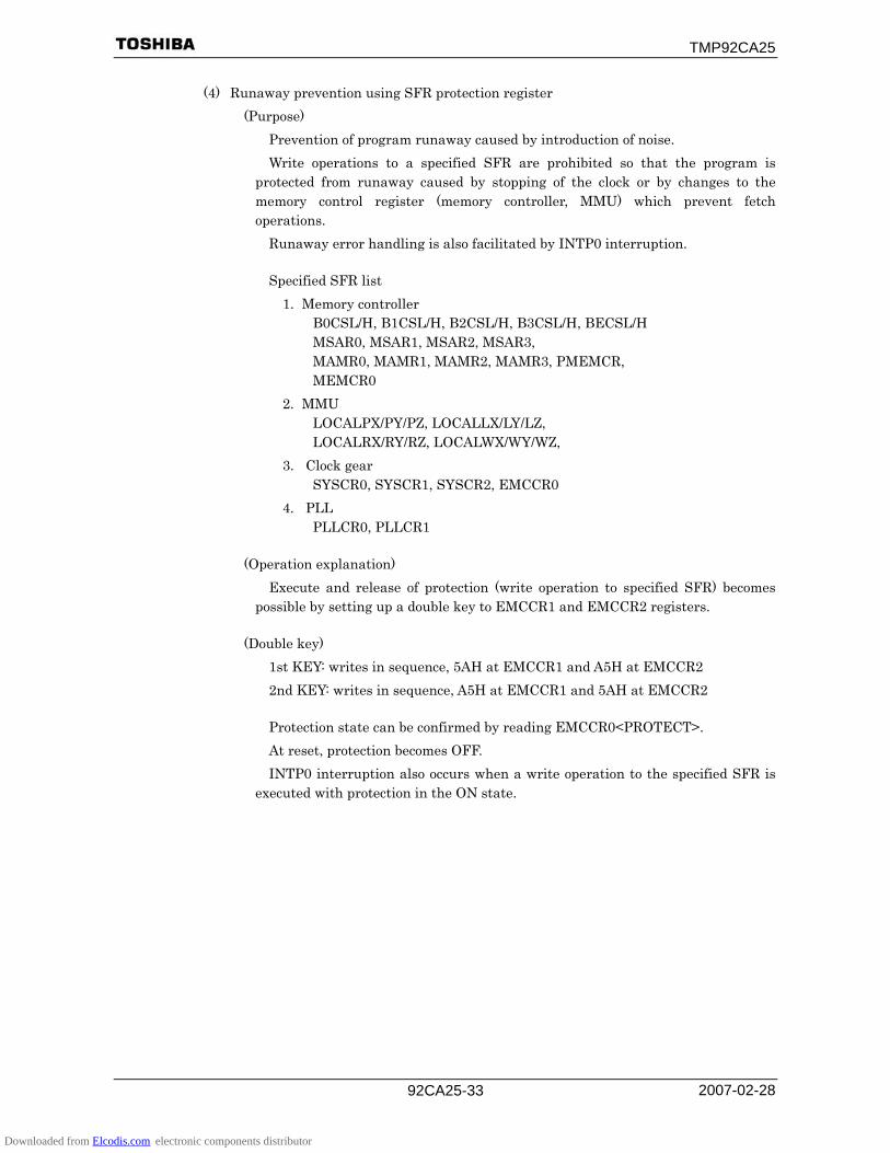
(4) Runaway prevention using SFR protection register (Purpose)
Prevention of program runaway caused by introduction of noise. Write operations to a specified SFR are prohibited so that the program is
protected from runaway caused by stopping of the clock or by changes to the memory control register (memory controller, MMU) which prevent fetch operations.
Runaway error handling is also facilitated by INTP0 interruption.
Specified SFR list 1. Memory controller
B0CSL/H, B1CSL/H, B2CSL/H, B3CSL/H, BECSL/H MSAR0, MSAR1, MSAR2, MSAR3, MAMR0, MAMR1, MAMR2, MAMR3, PMEMCR, MEMCR0
2. MMU LOCALPX/PY/PZ, LOCALLX/LY/LZ, LOCALRX/RY/RZ, LOCALWX/WY/WZ,
3. Clock gear SYSCR0, SYSCR1, SYSCR2, EMCCR0
4. PLL PLLCR0, PLLCR1
(Operation explanation)
Execute and release of protection (write operation to specified SFR) becomes possible by setting up a double key to EMCCR1 and EMCCR2 registers.
(Double key)
1st KEY: writes in sequence, 5AH at EMCCR1 and A5H at EMCCR2 2nd KEY: writes in sequence, A5H at EMCCR1 and 5AH at EMCCR2
Protection state can be confirmed by reading EMCCR0<PROTECT>. At reset, protection becomes OFF. INTP0 interruption also occurs when a write operation to the specified SFR is
executed with protection in the ON state.
Downloaded from Elcodis.com electronic components distributor
TMP92CA25
2007-02-28 92CA25-34
3.3.6 Stand-by Controller
(1) HALT modes and port drive register When the HALT instruction is executed, the operating mode switches to IDLE2,
IDLE1 or STOP mode, depending on the contents of the SYSCR2<HALTM1:0> register and each pin-status is set according to the PxDR register, as shown below:
7 6 5 4 3 2 1 0
Bit symbol Px7D Px6D Px5D Px4D Px3D Px2D Px1D Px0D
Read/Write R/W After reset 1 1 1 1 1 1 1 1 Function Output/input buffer drive register for stand-by mode
(Purpose and use)
• This register is used to set each pin status at stand-by mode.
• All ports have this registers of the format shown above. (“x” indicates the port name.)
• For each register, refer to 3.5 function of ports.
• Before “Halt” instruction is executed, set each register according to the expected pin status. They will be effective
after the CPU has executed the “Halt” instruction.
• This is the case regardless of stand-by mode (IDLE2, IDLE1 or STOP).
• The Output/Input buffer control table is shown below.
OE PxnD Output Buffer Input Buffer0 0 OFF OFF 0 1 OFF ON 1 0 OFF OFF 1 1 ON OFF
Note 1: OE denotes an output enable signal before stand-by mode.
Basically, PxCR is used as OE.
Note 2: “n” in PxnD denotes the bit number of PORTx
The subsequent actions performed in each mode are as follows: 1. IDLE2: only the CPU halts.
The internal I/O is available to select operation during IDLE2 mode by setting the following register.
Table 3.3.2 shows the register setting operation during IDLE2 mode.
Table 3.3.2 SFR Setting Operation during IDLE2 Mode
Internal I/O SFR TMRA01 TA01RUN<I2TA01> TMRA23 TA23RUN<I2TA23> TMRB0 TB0RUN<I2TB0> SIO0 SC0MOD1<I2S0> I2C bus SBI0BR0<I2SBI0> AD converter ADMOD1<I2AD> WDT WDMOD<I2WDT>
2. IDLE1: Only the oscillator, RTC (real-time clock) and MLD continue to operate. 3. STOP: All internal circuits stop operating.
PxDR (xxxxH)
Downloaded from Elcodis.com electronic components distributor

TMP92CA25
2007-02-28 92CA25-35
The operation of each of the different HALT modes is described in Table 3.3.3.
Table 3.3.3 I/O Operation during HALT Modes
HALT Mode IDLE2 IDLE1 STOP
SYSCR2<HALTM1:0> 11 10 01 CPU Stop I/O ports Depend on PxDR register setting TMRA, TMRB SIO, SBI AD converter WDT
Available to select operation block
I2S, LCDC, SDRAMC, Interrupt controller, USBC,
Stop Block
RTC, MLD
Operate
Operate
(2) How to release the HALT mode These halt states can be released by resetting or requesting an interrupt. The halt
release sources are determined by the combination of the states of the interrupt mask register <IFF2:0> and the HALT modes. The details for releasing the halt status are shown in Table 3.3.4.
• Release by interrupt requesting
The HALT mode release method depends on the status of the enabled interrupt .When the interrupt request level set before executing the HALT instruction exceeds the value of the interrupt mask register, the interrupt is processed depending on its status after the HALT mode is released, and the CPU status executing the instruction that follows the HALT instruction. When the interrupt request level set before executing the HALT instruction is less than the value of the interrupt mask register, HALT mode release is not executed. (in non-maskable interrupts, interrupt processing is processed after releasing the HALT mode regardless of the value of the mask register.) However only for INT0 to INT4, INTKEY, INTRTC, INTALM and interrupts, even if the interrupt request level set before executing the halt instruction is less than the value of the interrupt mask register, HALT mode release is executed. In this case, the interrupt is processed, and the CPU starts executing the instruction following the HALT instruction, but the interrupt request flag is held at “1”.
• Release by resetting
Release of all halt statuses is executed by resetting. When the STOP mode is released by RESET, it is necessary to allow enough
resetting time (see Table 3.3.5) for operation of the oscillator to stabilize. When releasing the HALT mode by resetting, the internal RAM data keeps the
state before the HALT instruction is executed. However the other settings contents are initialized. (Releasing due to interrupts keeps the state before the HALT instruction is executed.)
Downloaded from Elcodis.com electronic components distributor

TMP92CA25
2007-02-28 92CA25-36
Table 3.3.4 Source of Halt State Clearance and Halt Clearance Operation
Status of Received Interrupt Interrupt Enabled
(Interrupt level) ≥ (Interrupt mask)
Interrupt Disabled (Interrupt level) < (Interrupt mask)
HALT Mode IDLE2 IDLE1 STOP IDLE2 IDLE1 STOPINTWD ♦ × × − − −
INT0 to INT4 (Note 1) ♦ ♦ ♦*1 ○ ○ ○*1 INTALM0 to INTALM4 ♦ ♦ × ○ ○ ×
INTTA0 to INTTA3, INTTB0 to INTTB1
♦ × × × × ×
INTRX0 to INTTX0, INTSBI ♦ × × × × ×
INTTBO0, INTI2S ♦ × × × × ×
INTAD, INT5, INTSPI ♦ × × × × ×
INTKEY ♦ ♦ ♦*1 ○ ○ ○*1 INTRTC ♦ ♦ ♦*1 ○ ○ ○*1
Inte
rrupt
INTLCD ♦ × × × × ×
Sou
rce
of H
alt S
tate
Cle
aran
ce
RESET Initialize LSI
♦: After clearing the HALT mode, CPU starts interrupt processing.
○: After clearing the HALT mode, CPU resumes executing starting from the instruction following the HALT instruction.
×: Cannot be used to release the HALT mode.
−: The priority level (interrupt request level) of non-maskable interrupts is fixed to 7, the highest priority level. This combination is not available.
*1: Release of the HALT mode is executed after warm-up time has elapsed.
Note 1: When the HALT mode is cleared by an INT0 interrupt of the level mode in the interrupt enabled status, hold level H until starting interrupt processing. If level L is set before holding level L, interrupt processing is correctly started.
Example: Releasing IDLE1 mode An INT0 interrupt clears the halt state when the device is in IDLE1 mode.
Address 8200H LD (PCFC), 01H ; Sets PC0 to INT0. 8203H LD (IIMC), 00H ; Selects INT0 interrupt rising edge. 8206H LD (INTE0AD), 06H ; Sets INT0 interrupt level to 6. 8209H EI 5 ; Sets interrupt level to 5 for CPU. 820BH LD (SYSCR2), 28H ; Sets HALT mode to IDLE1 mode. 820EH HALT ; Halts CPU. INT0 INT0 interrupt routine RETI 820FH LD XX, XX
Downloaded from Elcodis.com electronic components distributor

TMP92CA25
2007-02-28 92CA25-37
(3) Operation
1. IDLE2 mode In IDLE2 mode only specific internal I/O operations, as designated by the
IDLE2 setting register, can take place. Instruction execution by the CPU stops. Figure 3.3.7 illustrates an example of the timing for clearance of the IDLE2
mode halt state by an interrupt.
Figure 3.3.7 Timing Chart for IDLE2 Mode Halt State Cleared by Interrupt
2. IDLE1 mode In IDLE1 mode, only the internal oscillator and the RTC and MLD continue to
operate. The system clock stops. In the halt state, the interrupt request is sampled asynchronously with the
system clock; however, clearance of the halt state (e.g., restart of operation) is synchronous with it.
Figure 3.3.8 illustrates the timing for clearance of the IDLE1 mode halt state by an interrupt.
Figure 3.3.8 Timing Chart for IDLE1 Mode Halt State Cleared by Interrupt
Data Data
IDLE2mode
X1
A0 to A23
D0 to D15
RD
WR
Interrupt for release
Data Data
IDLE1mode
X1
A0 to A23
D0 to D15
RD
WR
Interrupt forrelease
Downloaded from Elcodis.com electronic components distributor

TMP92CA25
2007-02-28 92CA25-38
3. STOP mode When STOP mode is selected, all internal circuits stop, including the internal
oscillator. After STOP mode has been cleared system clock output starts when the
warm-up time has elapsed, in order to allow oscillation to stabilize. Figure 3.3.9 illustrates the timing for clearance of the STOP mode halt state by
an interrupt.
Figure 3.3.9 Timing Chart for STOP Mode Halt State Cleared by Interrupt
Table 3.3.5 Example of Warm-up Time after Releasing STOP Mode at fOSCH = 40 MHz, fs = 32.768 kHz
SYSCR2<WUPTM1:0> SYSCR1 <SYSCK> 01 (28) 10 (214) 11 (216)
0 (fc) 6.4 μs 409.6 μs 1.638 ms 1 (fs) 7.8 ms 500 ms 2000 ms
Data Data
STOP mode
X1
A0 to A23
D0 to D15
RD
WR
Interrupt forrelease
Warm-up time
Downloaded from Elcodis.com electronic components distributor

TMP92CA25
2007-02-28 92CA25-39
Table 3.3.6 Input Buffer State Table
Input Buffer State
In HALT mode (IDLE1/2/STOP) When the CPU is operating
<PxDR> = 1 <PxDR> = 0 Port Name Input Function Name During
Reset When used as
Function pin
When used as
Input pin
When used as
Function pin
When used as
Input pin
When used as
Function pin
When used as
Input pin D0~D7 D0~D7 − − −
P10~P17 D8~D15
ON upon external
read OFF OFF
P60~P67 −
OFF
− − − P71~P72 − − − −
P75 B/NDR P76 WAIT
ON ON OFF
P90 − − − − P91 RXD0
P92 0CTS , SCLK0
P93~P94 SDA, SCL P96 *1 INT4 P97 INT5
PA0~PA7*1 KI0-KI7 PC0 INT0 PC1 INT1 PC2 INT2 PC3 INT3
ON ON OFF
PC4~PC7 − PF0 −
− − −
PF1 RXD0
PF2 0CTS SCLK0
ON
ON
ON
ON
ON
OFF
PG0~PG2*2 − − − −
PG3 *2 ADTRG OFF
ON ON upon port
read ON OFF
ON
PJ5~PJ6 − − − −
PK4 SPDI ON ON OFF
PK5~PK5 −
PL4~PL5, PL7 −
− − −
PL6 BUSRQ ON ON OFF
PN0~PN7 − −
ON
−
ON
−
OFF
BE − RESET −
AM0, AM1 − ON − ON −
X1, XT1 −
ON
ON −
IDLE2/IDLE1:ON, STOP:OFF
ON: The buffer is always turned on. A current flows the input buffer if the input pin is not driven.
OFF: The buffer is always turned off.
−: No applicable
*1: Port having a pull-up/pull-down resistor.
*2: AIN input does not cause a current to flow through the buffer.
Downloaded from Elcodis.com electronic components distributor
TMP92CA25
2007-02-28 92CA25-40
Table 3.3.7 Output Buffer State Table (1/2) Output Buffer State
In HALT mode (IDLE1/2/STOP) When the CPU is operating
<PxDR> = 1 <PxDR> = 0 Port Name Output Function
Name During Reset When used
as Function pin
When used as
Output pin
When used as
Function pin
When used as
Output pin
When used as
Function pin
When used as
Output pin
D0~D7 D0~D7 − − −
P10~P17 D8~D15 OFF
ON upon external
write ON OFF
ON OFF
A0~A15 A16~A15, − − − P60~P67 A16~A23
P70 RD
ON
P71 WRLL ,NDRE P72 WRLU ,NDWE P73 EA24 P74 EA25 P75 R/W
ON ON
OFF
P76 −
OFF
− − − P80 0CS
P81 1CS , SDCS
P82 2CS , CSZA
P83 3CS
P84 CSZB , CE0ND
P85 CSZC , CE1ND
P86 CSZD
P87 CSZE
ON
P90 TXD0, I2SCKO
P91 I2SDO
P92 I2SWS
P93 SDA
P94 SCL
OFF
P95 CLK32KO ON
ON ON OFF
P96 PX
P97 PY OFF
ON
−
ON
−
OFF
−
ON: The buffer is always turned on. *1: Port having a pull-up/pull-down resistor. OFF: The buffer is always turned off. −: Not applicable
Downloaded from Elcodis.com electronic components distributor

TMP92CA25
2007-02-28 92CA25-41
Table 3.3.8 Output Buffer State Table (2/2) Output Buffer State
In HALT mode (IDLE1/2/STOP) When the CPU is operating
<PxDR> = 1 <PxDR> = 0 Port Name Output Function
Name During Reset When used as
Function pin
When used as
Output pin
When used as
Function pin
When used as
Output pin
When used as
Function pin
When used as
Output pin
PC0 TA1OUT
PC1 TA3OUT
PC2 TB0OUT0
ON ON OFF
PC3 − − − − PC6 KO8, EA24
PC7 CSZF , EA25
PF0 TXD0
ON ON OFF
PF1 − − − − PF2 SCLK0
OFF
PF7 SDCLK ON
ON ON OFF
PG2 MX
PG3 MY OFF − − −
PJ0 SDRAS SRLLB
PJ1 SDCAS ,SRLUB
PJ2 SDWE , SRWR
PJ3 SDLLDQM
PJ4 SDLUDQM
ON
PJ5 NDALE
PJ6 NDCLE OFF
PJ7 SDCKE
PK0 LCP
PK1 LLP
PK2 LFR
PK3 LBCD
ON
ON ON OFF
PK4 − − − − PK5 SPDO
PK6 SPCS
PK7 SPCLK
OFF
PL0~PL3 LD0~LD3 ON PL4~PL6 LD4~LD6
PL7 LD7, BUSAK OFF
PM1 MLDALM
PM2 MLDALM , ALARM ON
PN0~PN7 KO0~KO7 OFF
ON ON
OFF
X2 − IDLE2/1:ON,
STOP: output ”H”
XT2 −
ON
−
− IDLE2/1:ON,
STOP: output ”HZ”
ON: The buffer is always turned on. *1: Port having a pull-up/pull-down resistor. OFF: The buffer is always turned off. −: Not applicable
Downloaded from Elcodis.com electronic components distributor

TMP92CA25
2007-02-28 92CA25-42
3.4 Interrupts
Interrupts are controlled by the CPU Interrupt mask register <IFF2:0> (bits12 to 14 of the status register) and by the built-in interrupt controller.
The TMP92CA25 has a total of 49 interrupts divided into the following five types:
Interrupts generated by CPU: 9 sources Software interrupts: 8 sources Illegal instruction interrupt: 1 source
Internal interrupts: 33 sources Internal I/O interrupts: 25 sources Micro DMA transfer end interrupts: 8 sources
External interrupts: 7 sources Interrupts on external pins (INT0 to INT5, INTKEY)
A fixed individual interrupt vector number is assigned to each interrupt source. Any one of six levels of priority can also be assigned to each maskable interrupt.
Non-maskable interrupts have a fixed priority level of 7, the highest level. When an interrupt is generated, the interrupt controller sends the priority of that interrupt
to the CPU. When more than one interrupt is generated simultaneously, the interrupt controller sends the priority value of the interrupt with the highest priority to the CPU. (The highest priority level is 7, the level used for non-maskable interrupts.)
The CPU compares the interrupt priority level which it receives with the value held in the CPU interrupt mask register <IFF2:0>. If the priority level of the interrupt is greater than or equal to the value in the interrupt mask register, the CPU accepts the interrupt.
However, software interrupts and illegal instruction interrupts generated by the CPU are processed irrespective of the value in <IFF2:0>.
The value in the interrupt mask register <IFF2:0> can be changed using the EI instruction (EI num sets <IFF2:0> to num). For example, the command EI 3 enables the acceptance of all non-maskable interrupts and of maskable interrupts whose priority level, as set in the interrupt controller, is 3 or higher. The commands EI and EI 0 enable the acceptance of all non-maskable interrupts and of maskable interrupts with a priority level of 1 or above (hence both are equivalent to the command EI 1).
The DI instruction (sets <IFF2:0> to 7) is exactly equivalent to the EI 7 instruction. The DI instruction is used to disable all maskable interrupts (since the priority level for maskable interrupts ranges from 1 to 6). The EI instruction takes effect as soon as it is executed.
In addition to the general purpose interrupt processing mode described above, there is also a micro DMA processing mode.
In micro DMA mode the CPU automatically transfers data in one-byte, two-byte or four-byte blocks; this mode allows high-speed data transfer to and from internal and external memory and internal I/O ports.
In addition, the TMP92CA25 also has a software start function in which micro DMA processing is requested in software rather than by an interrupt.
Figure 3.4.1 is a flowchart showing overall interrupt processing.
Downloaded from Elcodis.com electronic components distributor

TMP92CA25
2007-02-28 92CA25-43
Figure 3.4.1 Interrupt and Micro DMA Processing Sequence
Micro DMA soft start request
Interrupt processing
Interrupt vector calue “V” read interrupt request F/F clear
Interrupt specified by micro DMA start vector ?
PUSH PC PUSH SR SR<IFF2:0> ← Level of
accepted interrupt + 1
INTNEST ← INTNEST + 1
PC ← (FFFF00H + V)
Interrupt processing program
RETI instruction POP SR POP PC
INTNEST ← INTNEST − 1
End
Clear interrupt request flag
YES
NO
Data transfer by micro DMA
COUNT ← COUNT − 1
COUNT = 0
NO
Clear vector registergenerating micro DMA transfer end interrupt
(INTTC0 to 7)
YES
Micro DMA processing
General-purpose interrupt
processing
Downloaded from Elcodis.com electronic components distributor

TMP92CA25
2007-02-28 92CA25-44
3.4.1 General-purpose Interrupt Processing
When the CPU accepts an interrupt, it usually performs the following sequence of operations. However, in the case of software interrupts and illegal instruction interrupts generated by the CPU, the CPU skips steps (1) and (3), and executes only steps (2), (4) and (5). (1) The CPU reads the interrupt vector from the interrupt controller.
When more than one interrupt with the same priority level has been generated simultaneously, the interrupt controller generates an interrupt vector in accordance with the default priority and clears the interrupt requests.
(The default priority is determined as follows: the smaller the vector value, the higher the priority.)
(2) The CPU pushes the program counter (PC) and status register (SR) onto the top of the stack (pointed to by XSP).
(3) The CPU sets the value of the CPU’s interrupt mask register <IFF2:0> to the priority level for the accepted interrupt plus 1. However, if the priority level for the accepted interrupt is 7, the register’s value is set to 7.
(4) The CPU increments the interrupt nesting counter INTNEST by 1.
(5) The CPU jumps to the address given by adding the contents of address FFFF00H + the interrupt vector, then starts the interrupt processing routine.
On completion of interrupt processing, the RETI instruction is used to return control to
the main routine. RETI restores the contents of the program counter and the status register from the stack and decrements the interrupt nesting counter INTNEST by 1.
Non-maskable interrupts cannot be disabled by a user program. Maskable interrupts, however, can be enabled or disabled by a user program. A program can set the priority level for each interrupt source. (A priority level setting of 0 or 7 will disable an interrupt request.)
If an interrupt request is received for an interrupt with a priority level equal to or greater than the value set in the CPU interrupt mask register <IFF2:0>, the CPU will accept the interrupt. The CPU interrupt mask register <IFF2:0> is then set to the value of the priority level for the accepted interrupt plus 1.
If during interrupt processing, an interrupt is generated with a higher priority than the interrupt currently being processed, or if, during the processing of a non-maskable interrupt processing, a non-maskable interrupt request is generated from another source, the CPU will suspend the routine which it is currently executing and accept the new interrupt. When processing of the new interrupt has been completed, the CPU will resume processing of the suspended interrupt.
If the CPU receives another interrupt request while performing processing steps (1) to (5), the new interrupt will be sampled immediately after execution of the first instruction of its interrupt processing routine. Specifying DI as the start instruction disables nesting of maskable interrupts.
A reset initializes the interrupt mask register <IFF2:0> to 111, disabling all maskable
interrupts. Table 3.4.1 shows the TMP92CA25 interrupt vectors and micro DMA start vectors.
FFFF00H to FFFFFFH (256 bytes) is designated as the interrupt vector area.
Downloaded from Elcodis.com electronic components distributor

TMP92CA25
2007-02-28 92CA25-45
Table 3.4.1 TMP92CA25 Interrupt Vectors and Micro DMA Start Vectors
Default Priority Type
Interrupt Source and Source of Micro DMA Request
Vector Value
Address Refer to Vector
Micro DMA Start
Vector 1 Reset or [SWI0] instruction 0000H FFFF00H
2 [SWI1] instruction 0004H FFFF04H 3 Illegal instruction or [SWI2] instruction 0008H FFFF08H 4 [SWI3] instruction 000CH FFFF0CH 5 [SWI4] instruction 0010H FFFF10H 6 [SWI5] instruction 0014H FFFF14H 7 [SWI6] instruction 0018H FFFF18H 8 [SWI7] instruction 001CH FFFF1CH 9 (Reserved) 0020H FFFF20H
10
Non- maskable
INTWD: Watchdog Timer 0024H FFFF24H − Micro DMA − − − (Note1)
11 INT0: INT0 pin input 0028H FFFF28H 0AH (Note 2)
12 INT1: INT1 pin input 002CH FFFF2CH 0BH 13 INT2: INT2 pin input 0030H FFFF30H 0CH 14 INT3: INT3 pin input 0034H FFFF34H 0DH 15 INT4: INT4 pin input (TSI) 0038H FFFF38H 0EH 16 INTALM0: ALM0 (8192 Hz) 003CH FFFF3CH 0FH 17 INTALM1: ALM1 (512 Hz) 0040H FFFF40H 10H 18 INTALM2: ALM2 (64 Hz) 0044H FFFF44H 11H 19 INTALM3: ALM3 (2 Hz) 0048H FFFF48H 12H 20 INTALM4: ALM4 (1 Hz) 004CH FFFF4CH 13H 21 INTP0: Protect0 (Write to special SFR) 0050H FFFF50H 14H 22 (Reserved) 0054H FFFF54H 15H 23 INTTA0: 8-bit timer 0 0058H FFFF58H 16H 24 INTTA1: 8-bit timer 1 005CH FFFF5CH 17H 25 INTTA2: 8-bit timer 2 0060H FFFF60H 18H 26 INTTA3: 8-bit timer 3 0064H FFFF64H 19H 27 INTTB0: 16-bit timer 0 0068H FFFF68H 1AH 28 INTTB1: 16-bit timer 0 006CH FFFF6CH 1BH 29 INTKEY: Key-on wakeup 0070H FFFF70H 1CH 30 INTRTC: RTC (Alarm interrupt) 0074H FFFF74H 1DH 31 INTTBO0: 16-bit timer 0 (Overflow) 0078H FFFF78H 1EH 32 INTLCD: LCDC/LP pin 007CH FFFF7CH 1FH 33 INTRX0: Serial receive (Channel 0) 0080H FFFF80H 20H (Note 2)
34 INTTX0: Serial transmission (Channel 0) 0084H FFFF84H 21H 35 (Reserved) 0088H FFFF88H 22H (Note 2)
36 (Reserved) 008CH FFFF8CH 23H 37 (Reserved) 0090H FFFF90H 24H 38 (Reserved) 0094H FFFF94H 25H 39 INT5: INT5 pin input 0098H FFFF98H 26H 40 INTI2S: I2S (Channel 0) 009CH FFFF9CH 27H 41 INTNDF0 (NAND flash controller channel 0) 00A0H FFFFA0H 28H 42 INTNDF1 (NAND flash controller channel 1) 00A4H FFFFA4H 29H 43 INTSPI: SPIC 00A8H FFFFA8H 2AH 44 INTSBI: SBI 00ACH FFFFACH 2BH
45 (Reserved) 00B0H FFFFB0H 2CH
46 (Reserved) 00B4H FFFFB4H 2DH 47 (Reserved) 00B8H FFFFB8H 2EH 48 (Reserved) 00BCH FFFFBCH 2FH 49 (Reserved) 00C0H FFFFC0H 30H 50
Maskable
(Reserved) 00C4H FFFFC4H 31H
Downloaded from Elcodis.com electronic components distributor

TMP92CA25
2007-02-28 92CA25-46
Default Priority Type
Interrupt Source and Source of Micro DMA Request
Vector Value
Address Refer to Vector
Micro DMA Start
Vector 51 (Reserved) 00C8H FFFFC8H 32H 52 INTAD: AD conversion end 00CCH FFFFCCH 33H 53 INTTC0: Micro DMA end (Channel 0) 00D0H FFFFD0H 34H 54 INTTC1: Micro DMA end (Channel 1) 00D4H FFFFD4H 35H 55 INTTC2: Micro DMA end (Channel 2) 00D8H FFFFD8H 36H 56 INTTC3: Micro DMA end (Channel 3) 00DCH FFFFDCH 37H 57 INTTC4: Micro DMA end (Channel 4) 00E0H FFFFE0H 38H 58 INTTC5: Micro DMA end (Channel 5) 00E4H FFFFE4H 39H 59 INTTC6: Micro DMA end (Channel 6) 00E8H FFFFE8H 3AH 60 INTTC7: Micro DMA end (Channel 7) 00ECH FFFFECH 3BH − to −
Maskable
(Reserved) 00F0H
: 00FCH
FFFFF0H :
FFFFFCH
− to −
Note 1: Micro DMA default priority. Micro DMA initiation takes priority over other maskable interrupts.
Note 2: When initiating micro DMA, set at edge detect mode.
Downloaded from Elcodis.com electronic components distributor
TMP92CA25
2007-02-28 92CA25-47
3.4.2 Micro DMA Processing
In addition to general purpose interrupt processing, the TMP92CA25 also includes a micro DMA function. Micro DMA processing for interrupt requests set by micro DMA is performed at the highest priority level for maskable interrupts (level 6), regardless of the priority level of the interrupt source.
Because the micro DMA function is implemented through the CPU, when the CPU is placed in a stand-by state by a Halt instruction, the requirements of the micro DMA will be ignored (pending).
Micro DMA supports 8 channels and can be transferred continuously by specifying the micro DMA burst function as below.
Note: When using the micro DMA transfer end interrupt, always write “1” to bit 7 of SIMC register.
(1) Micro DMA operation When an interrupt request is generated by an interrupt source specified by the micro
DMA start vector register, the micro DMA triggers a micro DMA request to the CPU at interrupt priority level 6 and starts processing the request. The eight micro DMA channels allow micro DMA processing to be set for up to eight types of interrupt at once.
When micro DMA is accepted, the interrupt request flip-flop assigned to that channel is cleared. Data in one-byte, two-byte or four-byte blocks, is automatically transferred at once from the transfer source address to the transfer destination address set in the control register, and the transfer counter is decremented by 1. If the value of the counter after it has been decremented is not 0, DMA processing ends with no change in the value of the micro DMA start vector register. If the value of the decremented counter is 0, a micro DMA transfer end interrupt (INTTC0 to INTTC7) is sent from the CPU to the interrupt controller. In addition, the micro DMA start vector register is cleared to 0, the next micro DMA operation is disabled and micro DMA processing terminates.
If micro DMA requests are set simultaneously for more than one channel, priority is not based on the interrupt priority level but on the channel number: the lower the channel number, the higher the priority (channel 0 thus has the highest priority and channel 7 the lowest).
If an interrupt request is triggered for the interrupt source in use during the interval between the time at which the micro DMA start vector is cleared and the next setting, general purpose interrupt processing is performed at the interrupt level set. Therefore, if the interrupt is only being used to initiate micro DMA (and not as a general-purpose interrupt), the interrupt level should first be set to 0 (i.e., interrupt requests should be disabled).
If micro DMA and general purpose interrupts are being used together as described above, the level of the interrupt which is being used to initiate micro DMA processing should first be set to a lower value than all the other interrupt levels. (Note) In this case, edge triggered interrupts are the only kinds of general interrupts which can be accepted.
Note: If the priority level of micro DMA is set higher than that of other interrupts, CPU operates as follows. In case INTxxx interrupt is generated first and then INTyyy interrupt is generated between checking “Interrupt specified by micro DMA start vector” (in the Figure 3.4.1) and reading interrupt vector with setting below. The vector shifts to that of INTyyy at the time. This is because the priority level of INTyyy is higher than that of INTxxx. In the interrupt routine, CPU reads the vector of INTyyy because cheking of micro DMA has finished. And INTyyy is generated regardless of transfer counter of micro DMA. INTxxx: level 1 without micro DMA INTyyy: level 6 with micro DMA
Downloaded from Elcodis.com electronic components distributor

TMP92CA25
2007-02-28 92CA25-48
Although the control registers used for setting the transfer source and transfer
destination addresses are 32 bits wide, this type of register can only output 24-bit addresses. Accordingly, micro DMA can only access 16 Mbytes (the upper eight bits of a 32-bit address are not valid).
Three micro DMA transfer modes are supported: one-byte transfers, two-byte (one-word) transfer and four-byte transfer. After a transfer in any mode, the transfer source and transfer destination addresses will either be incremented or decremented, or will remain unchanged. This simplifies the transfer of data from memory to memory, from I/O to memory, from memory to I/O, and from I/O to I/O. For details of the various transfer modes, see section 3.4.2 (1), detailed description of the transfer mode register.
Since a transfer counter is a 16-bit counter, up to 65536 micro DMA processing operations can be performed per interrupt source (provided that the transfer counter for the source is initially set to 0000H).
Micro DMA processing can be initiated by any one of 34 different interrupts – the 33 interrupts shown in the micro DMA start vectors in Table 3.4.1 and a micro DMA soft start.
Figure 3.4.2 shows a 2-byte transfer carried out using a micro DMA cycle in transfer destination address INC mode (micro DMA transfers are the same in every mode except counter mode). (The conditions for this cycle are as follows: Both source and destination memory are internal RAM and multiples by 4 numbered source and destination addresses.)
Note: In fact, src and dst address are not output to A23 to A0 pins
because they are internal RAM address.
Figure 3.4.2 Timing for Micro DMA Cycle State (1), (2): Instruction fetch cycle (Prefetches the next instruction code) State (3): Micro DMA read cycle State (4): Micro DMA write cycle State (5): (The same as in state (1), (2))
src
1 state
fSYS
A23 to A0
(1)
dst
(2) (3) (4) (5)
Downloaded from Elcodis.com electronic components distributor

TMP92CA25
2007-02-28 92CA25-49
(2) Soft start function The TMP92CA25 can initiate micro DMA either with an interrupt or by using the
micro DMA soft start function, in which micro DMA is initiated by a write cycle which writes to the register DMAR.
Writing 1 to any bit of the register DMAR causes micro DMA to be performed once. (If write “0” to each bit, micro DMA doesn’t operate). On completion of the transfer, the bits of DMAR which support the end channel are automatically cleared to 0.
Only one channel can be set for DMA request at once. (Do not write “1” to plural bits.)
When writing again 1 to the DMAR register, check whether the bit is “0” before writing “1”. If read “1”, micro DMA transfer isn’t started yet.
When a burst is specified by the DMAB register, data is transferred continuously from the initiation of micro DMA until the value in the micro DMA transfer counter is 0. If execatee soft start during micro DMA transfer by interrupt source, micro DMA transfer counter doesn’t change. Don’t use Read-modify-write instruction to avoid writign to other bits by mistake.
Symbol Name Address 7 6 5 4 3 2 1 0 DREQ7 DREQ6 DREQ5 DREQ4 DREQ3 DREQ2 DREQ1 DREQ0
R/W 0 0 0 0 0 0 0 0
DMAR DMA
Request
109H (Prohibit RMW)
1: DMA request in software
(3) Transfer control registers The transfer source address and the transfer destination address are set in the
following registers. An instruction of the form LDC cr, r can be used to set these registers.
Channel 0 DMAS0 DMA source address register 0 DMAD0 DMA destination address register 0
DMAC0 DMA counter register 0 DMAM0 DMA mode register 0
Channel 7 DMAS7 DMA source address register 7 DMAD7 DMA destination address register 7
DMAC7 DMA counter register 7 DMAM7 DMA mode register 7
8 bits
16 bits
32 bits
Downloaded from Elcodis.com electronic components distributor
TMP92CA25
2007-02-28 92CA25-50
(4) Detailed description of the transfer mode register
0 0 0 Mode DMAM0 to DMAM7
DMAMn[4:0] Mode Description Execution State Number
0 0 0 z z Destination INC mode (DMADn+) ← (DMASn) DMACn ← DMACn − 1 if DMACn = 0 then INTTCn
5 states
0 0 1 z z Destination DEC mode (DMADn−) ← (DMASn) DMACn ← DMACn − 1 if DMACn = 0 then INTTCn
5 states
0 1 0 z z Source INC mode (DMADn) ← (DMASn+) DMACn ← DMACn − 1 if DMACn = 0 then INTTCn
5 states
0 1 1 z z Source DEC mode (DMADn) ← (DMASn−) DMACn ← DMACn − 1 if DMACn = 0 then INTTCn
5 states
1 0 0 z z Source and destination INC mode (DMADn+) ← (DMASn+) DMACn ← DMACn − 1 If DMACn = 0 then INTTCn
6 states
1 0 1 z z Source and destination DEC mode (DMADn−) ← (DMASn−) DMACn ← DMACn − 1 If DMACn = 0 then INTTCn
6 states
1 1 0 z z Source and destination Fixed mode (DMADn) ← (DMASn) DMACn ← DMACn − 1 If DMACn = 0 then INTTCn
5 states
1 1 1 0 0 Counter mode DMASn ← DMASn + 1 DMACn ← DMACn − 1 if DMACn = 0 then INTTCn
5 states
ZZ: 00 = 1-byte transfer 01 = 2-byte transfer 10 = 4-byte transfer 11 = (Reserved)
Note1: N stands for the micro DMA channel number (0 to 7) DMADn+/DMASn+: Post-increment (register value is incremented after transfer) DMADn−/DMASn−: Post-decrement (register value is decremented after transfer) “I/O” signifies fixed memory addresses; “memory” signifies incremented or decremented memory addresses.
Note2: The transfer mode register should not be set to any value other than those listed above.
Note3: The execution state number shows number of best case (1-state memory access).
Downloaded from Elcodis.com electronic components distributor
TMP92CA25
2007-02-28 92CA25-51
3.4.3 Interrupt Controller Operation
The block diagram in Figure 3.4.3 shows the interrupt circuits. The left hand side of the diagram shows the interrupt controller circuit. The right hand side shows the CPU interrupt request signal circuit and the halt release circuit.
For each of the 52 interrupts channels there is an interrupt request flag (consisting of a flip-flop), an interrupt priority setting register and a micro DMA start vector register. The interrupt request flag latches interrupt requests from the peripherals. The flag is cleared to zero in the following cases: when a reset occurs, when the CPU reads the channel vector of an interrupt it has received, when the CPU receives a micro DMA request (when micro DMA is set), when a micro DMA burst transfer is terminated, and when an instruction that clears the interrupt for that channel is executed (by writing a micro DMA start vector to the INTCLR register).
An interrupt priority can be set independently for each interrupt source by writing the priority to the interrupt priority setting register (e.g., INTE0AD or INTE12). 6 interrupt priorities levels (1 to 6) are provided. Setting an interrupt source’s priority level to 0 (or 7) disables interrupt requests from that source. The priority of non-maskable interrupt (watchdog timer interrupts) is fixed at 7. If more than one interrupt request with a given priority level are generated simultaneously, the default priority (the interrupt with the lowest priority or, in other words, the interrupt with the lowest vector value) is used to determine which interrupt request is accepted first.
The 3rd and 7th bit of the interrupt priority setting register indicate the state of the interrupt request flag and thus whether an interrupt request for a given channel has occurred.
If several interrupts are generated simultaneously, the interrupt controller sends the interrupt request for the interrupt with the highest priority and the interrupt’s vector address to the CPU. The CPU compares the mask value set in <IFF2:0> of the status register (SR) with the priority level of the requested interrupt; if the latter is higher, the interrupt is accepted. Then the CPU sets SR<IFF2:0> to the priority level of the accepted interrupt + 1. Hence, during processing of the accepted interrupt, new interrupt requests with a priority value equal to or higher than the value set in SR<IFF2:0> (e.g., interrupts with a priority higher than the interrupt being processed) will be accepted.
When interrupt processing has been completed (e.g., after execution of a RETI instruction), the CPU restores to SR<IFF2:0> the priority value which was saved on the stack before the interrupt was generated.
The interrupt controller also includes eight registers which are used to store the micro DMA start vector. Writing the start vector of the interrupt source for the micro DMA processing (see Table 3.4.1), enables the corresponding interrupts to be processed by micro DMA processing. The values must be set in the micro DMA parameter registers (e.g., DMAS and DMAD) prior to micro DMA processing.
Downloaded from Elcodis.com electronic components distributor

TMP92CA25
2007-02-28 92CA25-52
Figure 3.4.3 Block Diagram of Interrupt Controller
INT0
1 to
INT4
, IN
TKE
Y,IN
TRTC
, IN
TALM
Inte
rrup
t req
uest
si
gnal
to C
PU
if IF
F =
7 th
en 0
Mic
ro D
MA
star
t vec
tor s
ettin
g re
gist
er
INTT
C0
INTT
C1
INTT
C2
INTT
C3
INTT
C4
INTT
C5
INTT
C6
INTT
C7
V =
D0H
V
= D
4H
V =
D8H
V
= D
CH
V
= E
0H
V =
E4H
V
= E
8H
V =
EC
H
Sof
t sta
rt
Mic
ro D
MA
co
unte
r 0
inte
rrup
t
6
INTT
C0
Dur
ing
IDLE
1
45
3 3 3
1
6
1 7
3
3
8
6 51
8 in
put O
R
Mic
ro D
MA
cha
nnel
pr
iorit
y de
code
r
P
riorit
y en
code
r
DM
A0V
D
MA
1V
:
DM
A7V
RE
SE
T Inte
rrup
t req
uest
F/F
RE
SE
T
Dec
oder
Res
et P
riorit
y se
tting
regi
ster
V =
20H
V
= 2
4H
Inte
rrupt
con
trolle
r C
PU
S
Q
R
V =
28H
V
= 2
CH
V
= 3
0H
V =
34H
V
= 3
8H
V =
3C
H
V =
40H
V
= 4
4H
V =
48H
V
= 4
CH
D
Q
CLR
Y1
Y2
Y3
Y4
Y5
Y6
A
B
C
Dn
Dn
+ 1
Dn
+ 2
Inte
rrupt
re
ques
t F/F
Inte
rrup
t vec
tor r
ead
Mic
ro D
MA
ack
now
ledg
e
Inte
rrup
t req
uest
F/F
Dn
+ 3
A
B
C
inte
rrupt
ve
ctor
read
D2
D3
D4
D5
D6
D7
Sel
ecto
r
S
Q
R
0 1 2 3 4 5 6 7
A
B
C
D0
D1
Inte
rrup
t vec
tor
read
Inte
rrupt
m
ask
F/F
Mic
ro D
MA
requ
est
Hal
t rel
ease
If IN
TRQ
2 to
0 ≥
IFF
2 to
0 th
en 1
.
INTR
Q2
to 0
IFF2
to 0
Inte
rrupt
le
vel d
etec
t
RE
SE
T EI
1 to
7
DI
Inte
rrup
t req
uest
si
gnal
Dur
ing
STO
P
Mic
ro D
MA
cha
nnel
sp
ecifi
catio
n
RE
SE
T
INTW
D
INT0
INT1
IN
T2
INT3
IN
T4
INTA
LM0
INTA
LM1
INTA
LM2
INTA
LM3
INTA
LM4
S
In
terr
upt v
ecto
r ge
nera
tor
Hig
hest
pr
iorit
y in
terr
upt
leve
l sel
ect
1 2 3 4 5 6 7
D5
D4
D3
D2
D1
D0
D
Q
CLR
Downloaded from Elcodis.com electronic components distributor
TMP92CA25
2007-02-28 92CA25-53
(1) Interrupt level setting registers
Symbol Name Address 7 6 5 4 3 2 1 0 INTAD INT0
IADC IADM2 IADM1 IADM0 I0C I0M2 I0M1 I0M0 R R/W R R/W
INTE0AD
INT0 &
INTAD enable
F0H
0 0 0 0 0 0 0 0
INT2 INT1 I2C I2M2 I2M1 I2M0 I1C I1M2 I1M1 I1M0 R R/W R R/W
INTE12
INT1 &
INT2 enable
D0H
0 0 0 0 0 0 0 0
INT4 INT3 I4C I4M2 I4M1 I4M0 I3C I3M2 I3M1 I3M0 R R/W R R/W
INTE34
INT3 &
INT4 enable
D1H
0 0 0 0 0 0 0 0
INTI2S INT5 II2SC II2SM2 II2SM1 II2SM0 I5C I5M2 I5M1 I5M0
R R/W R R/W INTE5I2S
INT5 &
INTI2S enable
EBH
0 0 0 0 0 0 0 0
INTTA1 (TMRA1) INTTA0 (TMRA0) ITA1C ITA1M2 ITA1M1 ITA1M0 ITA0C ITA0M2 ITA0M1 ITA0M0
R R/W R R/W INTETA01
INTTA0 &
INTTA1 enable
D4H
0 0 0 0 0 0 0 0
INTTA3 (TMRA3) INTTA2 (TMRA2) ITA3C ITA3M2 ITA3M1 ITA3M0 ITA2C ITA2M2 ITA2M1 ITA2M0
R R/W R R/W INTETA23
INTTA2 &
INTTA3 enable
D5H
0 0 0 0 0 0 0 0
INTTB1 (TMRB1) INTTB0 (TMRB0) ITB1C ITB1M2 ITB1M1 ITB1M0 ITB0C ITB0M2 ITB0M1 ITB0M0
R R/W R R/W INTETB01
INTTB0 &
INTTB1 enable
D8H
0 0 0 0 0 0 0 0
− INTTBO0 − − − − ITBO0C ITBO0M2 ITBO0M1 ITBO0M0
R R/W INTETBO0
INTTBO0 (Overflow)
enable DAH
Note: Always write 0 0 0 0 0
INTTX0 INTRX0 ITX0C ITX0M2 ITX0M1 ITX0M0 IRX0C IRX0M2 IRX0M1 IRX0M0
R R/W R R/W INTES0
INTRX0 &
INTTX0 enable
DBH
0 0 0 0 0 0 0 0
INTTX1 − ITX1C ITX1M2 ITX1M1 ITX1M0 − − − −
R R/W INTESPI
INTSPI enable
E0H
0 0 0 0 Note: Always write 0
INTALM1 INTALM0 IA1C IA1M2 IA1M1 IA1M0 IA0C IA0M2 IA0M1 IA0M0
R R/W R R/W INTEALM01
INTALM0 & INTALM1
enable E5H
0 0 0 0 0 0 0 0
INTALM3 INTALM2 IA3C IA3M2 IA3M1 IA3M0 IA2C IA2M2 IA2M1 IA2M0
R R/W R R/W INTEALM23
INTALM2 & INTALM3
enable E6H
0 0 0 0 0 0 0 0
Downloaded from Elcodis.com electronic components distributor
TMP92CA25
2007-02-28 92CA25-54
Symbol Name Address 7 6 5 4 3 2 1 0
− INTALM4 − − − − IA4C IA4M2 IA4M1 IA4M0
R R/W INTEALM4
INTALM4 enable
E7H
Note: Always write 0 0 0 0 0
− INTRTC − − − − IRC IRM2 IRM1 IRM0
R R/W INTERTC
INTRTC enable
E8H
Note: Always write 0 0 0 0 0
− INTKEY − − − − IKC IKM2 IKM1 IKM0
R R/W INTEKEY
INTKEY enable
E9H
Note: Always write 0 0 0 0 0
− INTLCD − − − − ILCD1C ILCDM2 ILCDM1 ILCDM0
R R/W INTELCD
INTLCD enable
EAH
Note: Always write 0 0 0 0 0
INTNDF1 INTNDF0 IN1C IN1M2 IN1M1 IN1M0 IN0C IN0M2 IN0M1 IN0M0
R R/W R R/W INTEND01
INTNDF0 &
INTNDF1 enable
ECH
0 0 0 0 0 0 0 0
− INTP0 − − − − IP0C IP0M2 IP0M1 IP0M0
R R/W INTEP0
INTP0 enable
EEH
Note: Always write 0 0 0 0 0
lxxM2 lxxM1 lxxM0 Function (Write) 0 0 0 Disables interrupt requests 0 0 1 Sets interrupt priority level to 1 0 1 0 Sets interrupt priority level to 2 0 1 1 Sets interrupt priority level to 3 1 0 0 Sets interrupt priority level to 4 1 0 1 Sets interrupt priority level to 5 1 1 0 Sets interrupt priority level to 6 1 1 1 Disables interrupt requests
Interrupt request flag
Downloaded from Elcodis.com electronic components distributor

TMP92CA25
2007-02-28 92CA25-55
Interrupt request flag
Symbol Name Address 7 6 5 4 3 2 1 0 INTTC1 (DMA1) INTTC0 (DMA0)
ITC1C ITC1M2 ITC1M1 ITC1M0 ITC0C ITC0M2 ITC0M1 ITC0M0R R/W R R/W
INTETC01
INTTC0 &
INTTC1 enable
F1H
0 0 0 0 0 0 0 0
INTTC3 (DMA3) INTTC2 (DMA2) ITC3C ITC3M2 ITC3M1 ITC3M0 ITC2C ITC2M2 ITC2M1 ITC2M0
R R/W R R/W INTETC23
INTTC2 &
INTTC3 enable
F2H
0 0 0 0 0 0 0 0
INTTC5 (DMA5) INTTC4 (DMA4) ITC5C ITC5M2 ITC5M1 ITC5M0 ITC4C ITC4M2 ITC4M1 ITC4M0
R R/W R R/W INTETC45
INTTC4 &
INTTC5 enable
F3H
0 0 0 0 0 0 0 0
INTTC7 (DMA7) INTTC6 (DMA6) ITC7C ITC7M2 ITC7M1 ITC7M0 ITC6C ITC6M2 ITC6M1 ITC6M0
R R/W R R/W INTETC67
INTTC6 & INTTC7 enable
F4H
0 0 0 0 0 0 0 0
− INTWD − − − − ITCWD − − −
R INTWDT
INTWD enable
F7H
Note: Always write 0 0 − − −
lxxM2 lxxM1 lxxM0 Function (Write) 0 0 0 Disables interrupt requests 0 0 1 Sets interrupt priority level to 1 0 1 0 Sets interrupt priority level to 2 0 1 1 Sets interrupt priority level to 3 1 0 0 Sets interrupt priority level to 4 1 0 1 Sets interrupt priority level to 5 1 1 0 Sets interrupt priority level to 6 1 1 1 Disables interrupt requests
Downloaded from Elcodis.com electronic components distributor

TMP92CA25
2007-02-28 92CA25-56
(2) External interrupt control Symbol Name Address 7 6 5 4 3 2 1 0
I5EDGE I4EDGE I3EDGE I2EDGE I1EDGE I0EDGE I0LE −
W R/W 0 0 0 0 0 0 0 0
IIMC
Interrupt input mode control
F6H (Prohibit RMW)
INT5EDGE 0: Rising 1: Falling
INT4EDGE0: Rising 1: Falling
INT3EDGE0: Rising 1: Falling
INT2EDGE0: Rising 1: Falling
INT1EDGE0: Rising 1: Falling
INT0EDGE 0: Rising 1: Falling
0: INT0 edge mode
1: INT0 level mode
Always write “0”
*INT0 level enable
0 Edge detect INT 1 “H” level INT
Note 1: Disable INT0 request before changing INT0 pin mode from level sense to edge sense. Setting example:
DI LD (IIMC), XXXXXX00B ; Switches from level to edge. LD (INTCLR), 0AH ; Clears interrupt request flag. NOP ; Wait EI execution NOP NOP EI
X: Don’t care, −: No change.
Note 2: See electrical characteristics in section 4 for external interrupt input pulse width.
Settings of External Interrupt Pin Function
Interrupt Pin Name Mode Setting Method
Rising edge <I0LE> = 0, <I0EDGE> = 0
Falling edge <I0LE> = 0, <I0EDGE> = 1 INT0 PC0
High level <I0LE> = 1
Rising edge <I1EDGE> = 0 INT1 PC1
Falling edge <I1EDGE> = 1
Rising edge <I2EDGE> = 0 INT2 PC2
Falling edge <I2EDGE> = 1
Rising edge <I3EDGE> = 0 INT3 PC3
Falling edge <I3EDGE> = 1
Rising edge <I4EDGE> = 0 INT4 P96
Falling edge <I4EDGE> = 1
Rising edge <I5EDGE> = 0 INT5 P97
Falling edge <I5EDGE> = 1
Downloaded from Elcodis.com electronic components distributor

TMP92CA25
2007-02-28 92CA25-57
(3) SIO receive interrupt control
Symbol Name Address 7 6 5 4 3 2 1 0 − − IR0LE W W 0 1 1
SIMC
SIO interrupt
mode control
F5H (Prohibit RMW)
Always write “0” (Note)
Always write “0”
0: INTRX0 edge mode
1: INTRX0 level mode
Note: When using the micro DMA transfer end interrupt, always write “1”.
INTRX0 rising edge enable 0 Edge detect INTRX0 1 “H” level INTRX0
Downloaded from Elcodis.com electronic components distributor
TMP92CA25
2007-02-28 92CA25-58
(4) Interrupt request flag clear register The interrupt request flag is cleared by writing the appropriate micro DMA start
vector, as given in Table 3.4.1, to the register INTCLR. For example, to clear the interrupt flag INT0, perform the following register
operation after execution of the DI instruction. INTCLR ← 0AH Clears interrupt request flag INT0.
Symbol Name Address 7 6 5 4 3 2 1 0
CLRV7 CLRV6 CLRV5 CLRV4 CLRV3 CLRV2 CLRV1 CLRV0W
0 0 0 0 0 0 0 0 INTCLR
Interrupt clear
control
F8H (Prohibit RMW)
Interrupt vector
(5) Micro DMA start vector registers These registers assign micro DMA processing to sets which source corresponds to
DMA. The interrupt source whose micro DMA start vector value matches the vector set in one of these registers is designated as the micro DMA start source.
When the micro DMA transfer counter value reaches zero, the micro DMA transfer end interrupt corresponding to the channel is sent to the interrupt controller, the micro DMA start vector register is cleared, and the micro DMA start source for the channel is cleared. Therefore, in order for micro DMA processing to continue, the micro DMA start vector register must be set again during processing of the micro DMA transfer end interrupt.
If the same vector is set in the micro DMA start vector registers of more than one channel, the lowest numbered channel takes priority.
Accordingly, if the same vector is set in the micro DMA start vector registers for two different channels, the interrupt generated on the lower numbered channel is executed until micro DMA transfer is complete. If the micro DMA start vector for this channel has not been set in the channel’s micro DMA start vector register again, micro DMA transfer for the higher-numbered channel will be commenced. (This process is known as micro DMA chaining.)
Downloaded from Elcodis.com electronic components distributor

TMP92CA25
2007-02-28 92CA25-59
Symbol Name Address 7 6 5 4 3 2 1 0 DMA0V5 DMA0V4 DMA0V3 DMA0V2 DMA0V1 DMA0V0 R/W 0 0 0 0 0 0
DMA0V DMA0 start
vector 100H
DMA0 start vector
DMA1V5 DMA1V4 DMA1V3 DMA1V2 DMA1V1 DMA1V0 R/W 0 0 0 0 0 0
DMA1V DMA1 start
vector 101H
DMA1 start vector
DMA2V5 DMA2V4 DMA2V3 DMA2V2 DMA2V1 DMA2V0
R/W 0 0 0 0 0 0
DMA2V DMA2 start
vector 102H
DMA2 start vector
DMA3V5 DMA3V4 DMA3V3 DMA3V2 DMA3V1 DMA3V0
R/W 0 0 0 0 0 0
DMA3V DMA3 start
vector 103H
DMA3 start vector
DMA4V5 DMA4V4 DMA4V3 DMA4V2 DMA4V1 DMA4V0 R/W 0 0 0 0 0 0
DMA4V DMA4 start
vector 104H
DMA4 start vector
DMA5V5 DMA5V4 DMA5V3 DMA5V2 DMA5V1 DMA5V0 R/W 0 0 0 0 0 0
DMA5V DMA5 start
vector 105H
DMA5 start vector
DMA6V5 DMA6V4 DMA6V3 DMA6V2 DMA6V1 DMA6V0 R/W 0 0 0 0 0 0
DMA6V DMA6 start
vector 106H
DMA6 start vector
DMA7V5 DMA7V4 DMA7V3 DMA7V2 DMA7V1 DMA7V0 R/W 0 0 0 0 0 0
DMA7V DMA7 start
vector 107H
DMA7 start vector
Downloaded from Elcodis.com electronic components distributor
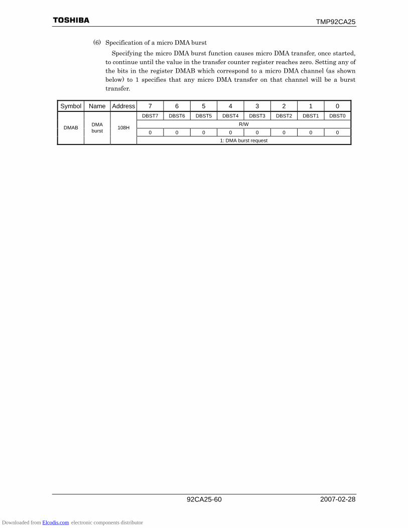
TMP92CA25
2007-02-28 92CA25-60
(6) Specification of a micro DMA burst Specifying the micro DMA burst function causes micro DMA transfer, once started,
to continue until the value in the transfer counter register reaches zero. Setting any of the bits in the register DMAB which correspond to a micro DMA channel (as shown below) to 1 specifies that any micro DMA transfer on that channel will be a burst transfer.
Symbol Name Address 7 6 5 4 3 2 1 0
DBST7 DBST6 DBST5 DBST4 DBST3 DBST2 DBST1 DBST0
R/W 0 0 0 0 0 0 0 0
DMAB DMA burst 108H
1: DMA burst request
Downloaded from Elcodis.com electronic components distributor

TMP92CA25
2007-02-28 92CA25-61
(7) Notes The instruction execution unit and the bus interface unit in this CPU operate
independently. Therefore, immediately before an interrupt is generated, if the CPU fetches an instruction which clears the corresponding interrupt request flag, the CPU may execute this instruction in between accepting the interrupt and reading the interrupt vector. In this case, the CPU will read the default vector 0004H and jump to interrupt vector address FFFF04H.
To avoid this, an instruction which clears an interrupt request flag should always be placed after a DI instruction. And in the case of setting an interrupt enable again by EI instruction after the execution of clearing instruction, execute EI instruction after clearing and more than 3−instructions (e.g., “NOP” × 3 times).
If it placed EI instruction without waiting NOP instruction after execution of clearing instruction, interrupt will be enabled before request flag is cleared.
In the case of changing the value of the interrupt mask register <IFF2:0> by execution of POP SR instruction, disable an interrupt by DI instruction before execution of POP SR instruction.
In addition, please note that the following two circuits are exceptional and demand special attention.
In level mode INT0 is not an edge triggered interrupt. Hence, in level mode the interrupt request flip-flop for INT0 does not function. The peripheral interrupt request passes through the S input of the flip-flop and becomes the Q output. If the interrupt input mode is changed from edge mode to level mode, the interrupt request flag is cleared automatically.
INT0 level mode
If the CPU enters the interrupt response sequence as a result of INT0 going from 0 to 1, INT0 must then be held at 1 until the interrupt response sequence has been completed. If INT0 is set to level mode so as to release a halt state, INT0 must be held at 1 from the time INT0 changes from 0 to 1 until the halt state is released. (Hence, it is necessary to ensure that input noise is not interpreted as a 0, causing INT0 to revert to 0 before the halt state has been released.) When the mode changes from level mode to edge mode, interrupt request flags which were set in level mode will not be cleared. Interrupt request flags must be cleared using the following sequence.
DI LD (IIMC), 00H ; Switches from level to edge. LD (INTCLR), 0AH ; Clears interrupt request flag. NOP ; Wait EI execution NOP NOP EI
INTRX In level mode (the register SIMC<IRxLE> set to “0”), the interrupt request flip-flop can only be cleared by a reset or by reading the serial channel receive buffer. It cannot be cleared by writing INTCLR register.
Note: The following instructions or pin input state changes are equivalent to instructions which clear the interrupt request flag.
INT0: Instructions which switch to level mode after an interrupt request has been generated in edge mode. The pin input changes from high to low after an interrupt request has been generated in level mode. (“H” → “L”) INTRX: Instructions which read the receive buffer.
INTRX: Instructions which read the receive buffer.
Downloaded from Elcodis.com electronic components distributor

TMP92CA25
2007-02-28 92CA25-62
3.5 Function of Ports
The TMP92CA25 I/O port pins are shown in Table 3.5.1 and Table 3.5.2. In addition to functioning as general-purpose I/O ports, these pins are also used by the internal CPU and I/O functions. Table 3.5.3 to Table 3.5.5 list the I/O registers and their specifications.
Table 3.5.1 Port Functions (1/2) (R: PD = with programmable pull-down resistor, U = with pull-up resistor)
Port Name Pin Name Number of Pins I/O R I/O Setting Pin Name for Built-in
Function Port 1 P10 to P17 8 I/O − Bit D8 to D15 Port 6 P60 to P67 8 I/O − Bit A16 to A23
P70 1 Output − (Fixed) RD P71 1 I/O − Bit WRLL , NDRE P72 1 I/O − Bit WRLU , NDWE P73 1 I/O − Bit EA24 P74 1 I/O − Bit EA25 P75 1 I/O − Bit R/ W , NDR/B
Port 7
P76 1 I/O − Bit WAIT P80 1 Output − (Fixed) 0CS P81 1 Output − (Fixed) 1CS , SDCS P82 1 Output − (Fixed) 2CS , CSZA P83 1 Output − (Fixed) 3CS P84 1 Output − (Fixed) CSZB , WRUL , CE0ND P85 1 Output − (Fixed) CSZC , WRUU , CE1ND P86 1 Output − (Fixed) CSZD
Port 8
P87 1 Output − (Fixed) CSZE P90 1 I/O − Bit TXD0, I2SCKO P91 1 I/O − Bit RXD0, I2SDO P92 1 I/O − Bit SCLK0, 0CTS , I2SWS P93 1 I/O − Bit SDA P94 1 I/O − Bit SCL P95 1 Output − (Fixed) CLK32KO P96 1 Input PD (Fixed) INT4, PX
Port 9
P97 1 Input − (Fixed) INT5, PY Port A PA0 to PA7 8 Input U (Fixed) KI0 to KI7
PC0 1 I/O − Bit INT0, TA1OUT PC1 1 I/O − Bit INT1, TA3OUT PC2 1 I/O − Bit INT2, TB0OUT0 PC3 1 I/O − Bit INT3 PC4 1 I/O − Bit PC5 1 I/O − Bit PC6 1 I/O − Bit KO8, EA24
Port C
PC7 1 I/O − Bit CSZF , EA25 PF0 1 I/O − Bit TXD0 PF1 1 I/O − Bit RXD0 PF2 1 I/O − Bit SCLK0, 0CTS PF3 1 I/O − Bit PF4 1 I/O − Bit PF5 1 I/O − Bit PF6 1 I/O − Bit
Port F
PF7 1 Output − (Fixed) SDCLK
Downloaded from Elcodis.com electronic components distributor

TMP92CA25
2007-02-28 92CA25-63
Table 3.5.2 Port Functions (2/2)
(R: PD = with programmable pull-down resistor, U = with pull-up resistor)
Port Name Pin Name Number of Pins I/O R I/O Setting Pin Name for Built-in Function
PG0 to PG1 2 Input − (Fixed) AN0 to AN1 PG2 1 Input − (Fixed) AN2, MX
Port G
PG3 1 Input − (Fixed) AN3, ADTRG , MY PJ0 1 Output − (Fixed) SDRAS , SRLLB PJ1 1 Output − (Fixed) SDCAS , SRLUB PJ2 1 Output − (Fixed) SDWE , SRWR PJ3 1 Output − (Fixed) SDLLDQM PJ4 1 Output − (Fixed) SDLUDQM PJ5 1 I/O − Bit NDALE PJ6 1 I/O − Bit NDCLE
Port J
PJ7 1 Output − (Fixed) SDCKE PK0 1 Output − (Fixed) LCP0 PK1 1 Output − (Fixed) LLP PK2 1 Output − (Fixed) LFR PK3 1 Output − (Fixed) LBCD PK4 1 I/O − Bit SPDI PK5 1 I/O − Bit SPDO PK6 1 I/O − Bit SPCS
Port K
PK7 1 I/O − Bit SPCLK PL0 to PL3 4 Output − (Fixed) LD0 to LD3 PL4 to PL5 2 I/O − Bit LD4 to LD5 PL6 1 I/O − Bit LD6, BUSRQ
Port L
PL7 1 I/O − Bit LD7, BUSAK PM1 1 Output − (Fixed) MLDALM Port M PM2 1 Output − (Fixed) ALARM , MLDALM
Port N PN0 to PN7 8 I/O − Bit KO0 to KO7
Downloaded from Elcodis.com electronic components distributor
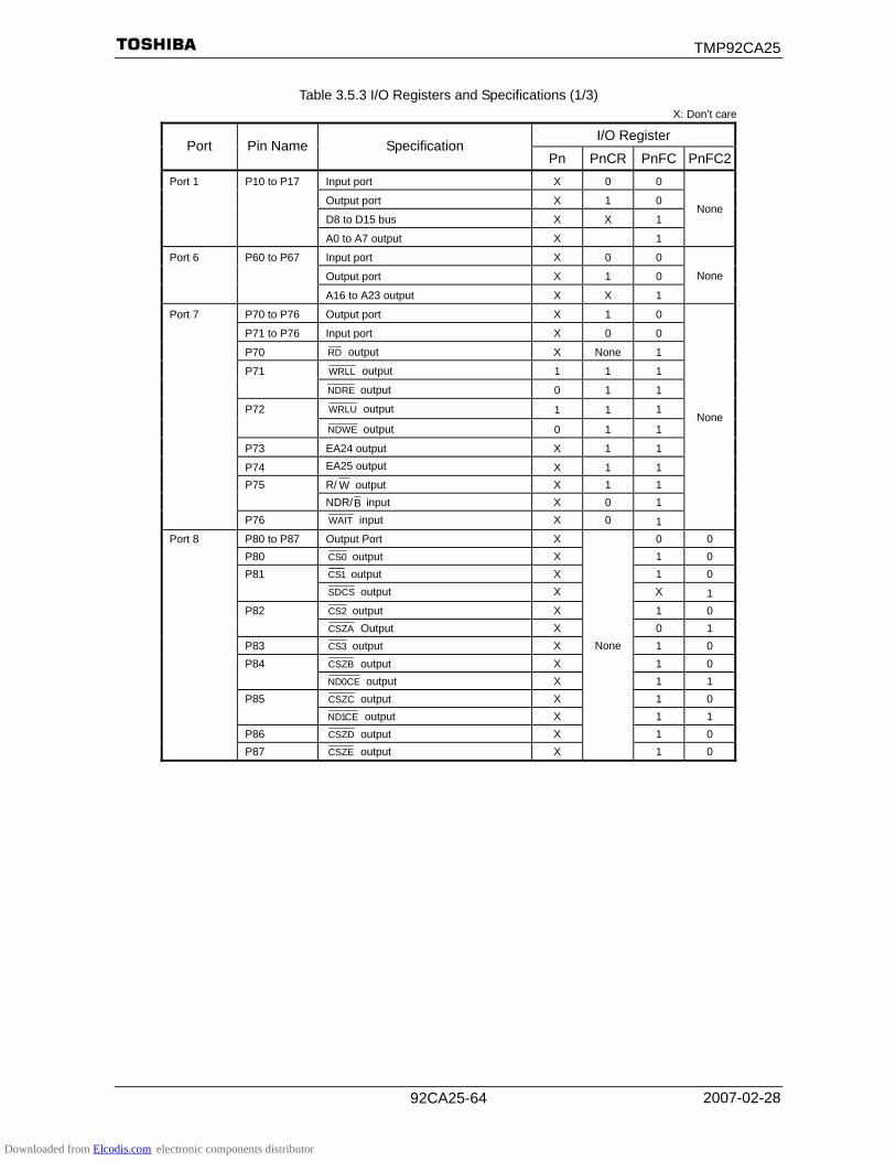
TMP92CA25
2007-02-28 92CA25-64
Table 3.5.3 I/O Registers and Specifications (1/3) X: Don’t care
I/O Register Port Pin Name Specification
Pn PnCR PnFC PnFC2Input port X 0 0
Output port X 1 0
D8 to D15 bus X X 1
Port 1 P10 to P17
A0 to A7 output X 1
None
Input port X 0 0
Output port X 1 0
Port 6 P60 to P67
A16 to A23 output X X 1
None
P70 to P76 Output port X 1 0
P71 to P76 Input port X 0 0
P70 RD output X None 1
WRLL output 1 1 1 P71 NDRE output 0 1 1
WRLU output 1 1 1 P72
NDWE output 0 1 1
P73 EA24 output X 1 1
P74 EA25 output X 1 1 R/ W output X 1 1 P75 NDR/B input X 0 1
Port 7
P76 WAIT input X 0 1
None
P80 to P87 Output Port X 0 0 P80 0CS output X 1 0
1CS output X 1 0 P81 SDCS output X X 1
2CS output X 1 0 P82 CSZA Output X 0 1
P83 3CS output X 1 0 CSZB output X 1 0 P84
CE0ND output X 1 1 CSZC output X 1 0 P85
CE1ND output X 1 1 P86 CSZD output X 1 0
Port 8
P87 CSZE output X
None
1 0
Downloaded from Elcodis.com electronic components distributor
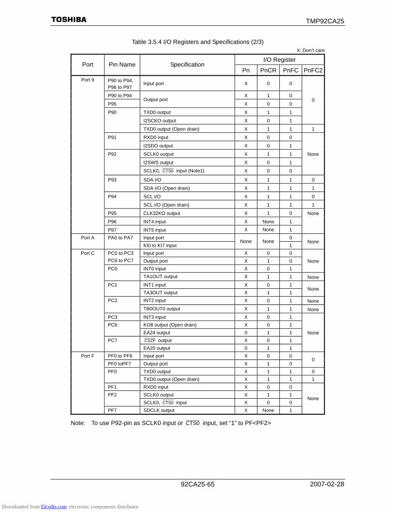
TMP92CA25
2007-02-28 92CA25-65
Table 3.5.4 I/O Registers and Specifications (2/3) X: Don’t care
I/O Register Port Pin Name Specification
Pn PnCR PnFC PnFC2P90 to P94, P96 to P97
Input port X 0 0
P90 to P94 X 1 0
P95 Output port
X 0 0
TXD0 output X 1 1
I2SCKO output X 0 1
0
P90
TXD0 output (Open drain) X 1 1 1
RXD0 input X 0 0 P91
I2SDO output X 0 1
SCLK0 output X 1 1
I2SWS output X 0 1
P92
SCLK0, 0CTS input (Note1) X 0 0
None
SDA I/O X 1 1 0 P93
SDA I/O (Open drain) X 1 1 1
SCL I/O X 1 1 0 P94
SCL I/O (Open drain) X 1 1 1
P95 CLK32KO output X 1 0
P96 INT4 input X None 1
Port 9
P97 INT5 input X None 1
None
Input port 0 Port A
PA0 to PA7 KI0 to KI7 input
None None 1
None
Input port X 0 0 PC0 to PC3 PC6 to PC7 Output port X 1 0
INT0 input X 0 1 None
PC0 TA1OUT output X 1 1 NoneINT1 input X 0 1 PC1 TA3OUT output X 1 1
None
INT2 input X 0 1 NonePC2
TB0OUT0 output X 1 1 NonePC3 INT3 input X 0 1
KO8 output (Open drain) X 0 1 PC6 EA24 output 0 1 1 CSZF output X 0 1
Port C
PC7 EA25 output 0 1 1
None
PF0 to PF6 Input port X 0 0 PF0 toPF7 Output port X 1 0
0
TXD0 output X 1 1 0 PF0 TXD0 output (Open drain) X 1 1 1
PF1 RXD0 input X 0 0 SCLK0 output X 1 1 PF2 SCLK0, 0CTS input X 0 0
Port F
PF7 SDCLK output X None 1
None
Note: To use P92-pin as SCLK0 input or 0CTS input, set “1” to PF<PF2>
Downloaded from Elcodis.com electronic components distributor

TMP92CA25
2007-02-28 92CA25-66
Table 3.5.5 I/O Registers and Specifications (3/3) X: Don’t care
I/O Register Port Pin Name Specification
Pn PnCR PnFC PnFC2Input port PG0 to PG3 AN0 to AN3 input
PG3 ADTRG input PG2 MX output
Port G
PG3 MY output
X None None None
PJ0 to PJ7 Output port X 1 0 PJ5 to PJ6 Input port X 0 0 PJ0 SDRAS , SRLLB output X 1 PJ1 SDCAS , SRLUB output X 1 PJ2 SDWE , SRWR output X 1 PJ3 SDLLDQM output X 1 PJ4 SDLUDQM output 1
None
1 PJ5 NDALE output 0 1 1 PJ6 NDCLE output 0 1 1
Port J
PJ7 SDCKE output X None 1
None
PK4 to PK7 Input port X 0 0 None PK0 to PK3 Output port X None 0 PK4 to PK7 Output port X 1 0 PK0 LCP0 output X 1 PK1 LLP output X 1 PK2 LFR output X 1 PK3 LBCD output X
None
1 PK4 SPDI input X 0 1 PK5 SPDO output X 1 1 PK6 SPCS output X 1 1
Port K
PK7 SPCLK output X 1 1
None
PL4 to PL7 Input Port X 0 0 PL0 to PL7 Output Port X 1 0 PL0 to PL7 LD0 to LD7 output X 1 1 PL6 BUSRQ input X 1 1
Port L
PL7 BUSAK output X 1 1
None
PM1 to PM2 Output Port X 0 PM1 MLDALM output X 1
MLDALM output 0 1
Port M
PM2 ALARM output 1
None
1
None
Input Port X 0 0 Output Port (CMOS output) X 1 0
Port N PN0 to PN7
KO output (Open drain output) X 1 1 None
Downloaded from Elcodis.com electronic components distributor

TMP92CA25
2007-02-28 92CA25-67
3.5.1 Port 1 (P10 to P17)
Port 1 is an 8-bit general-purpose I/O port. Bits can be individually set as either inputs or outputs by control register P1CR and function register P1FC.
In addition to functioning as a general-purpose I/O port, port1 can also function as a data bus (D8 to D15).
AM1 AM0 Function Setting after Reset is Released
0 0 Don’t use this setting 0 1 Data bus (D8 to D15) 1 0 Data bus (D8 to D15) 1 1 Input port
Figure 3.5.1 Port 1
P1CR register
P1FC register
P1 register
External write enable
D8 to D15
S0
1
S1
0
P10 to P17 (D8 to D15)
External read enable
D8 to D15
Port read data
Selector
Selector
Downloaded from Elcodis.com electronic components distributor

TMP92CA25
2007-02-28 92CA25-68
Port 1 register
7 6 5 4 3 2 1 0 Bit symbol P17 P16 P15 P14 P13 P12 P11 P10
Read/Write R/W After reset Data from external port (Output latch register is cleared to “0”)
Port 1 Control register
7 6 5 4 3 2 1 0 Bit symbol P17C P16C P15C P14C P13C P12C P11C P10C
Read/Write W After reset 0 0 0 0 0 0 0 0 Function 0: Input 1: Output
Port 1 Function register
7 6 5 4 3 2 1 0 Bit symbol P1F
Read/Write W After reset 0/1 Note 2Function 0: Port
1: Data bus (D8 to D15)
Port 1 Drive register
7 6 5 4 3 2 1 0 Bit symbol P17D P16D P15D P14D P13D P12D P11D P10D
Read/Write W After reset 1 1 1 1 1 1 1 1 Function Input/Output buffer drive register for standby mode
Note1: Read-modify-write is prohibited for P1CR and P1FC.
Note2: It is set to “Port” or “Data bus” by AM pin setting.
Figure 3.5.2 Register for Port 1
P1 (0004H)
P1CR (0006H)
P1FC (0007H)
P1DR (0081H)
Downloaded from Elcodis.com electronic components distributor

TMP92CA25
2007-02-28 92CA25-69
3.5.2 A0 to A7
A0 to A7 pin function is Address bus function only. Driver register is following register.
Port 4 Drive register 7 6 5 4 3 2 1 0
Bit symbol P57D P56D P55D P54D P53D P52D P51D P50D P4DR (0084H) Read/Write W
After reset 1 1 1 1 1 1 1 1 Function Input/Output buffer drive register for standby mode
Figure 3.5.3 Driver register for A0 to A7
3.5.3 A8 to A15
A8 to A15 pin function is Address bus function only. Driver register is following register.
Port 5 Drive register 7 6 5 4 3 2 1 0
Bit symbol P57D P56D P55D P54D P53D P52D P51D P50D P5DR (0085H) Read/Write W
After reset 1 1 1 1 1 1 1 1 Function Input/Output buffer drive register for standby mode
Figure 3.5.4 Drive register for A8 to A15
Downloaded from Elcodis.com electronic components distributor

TMP92CA25
2007-02-28 92CA25-70
3.5.4 Port 6 (P60 to P67)
Port 6 is an 8-bit general-purpose I/O port. Bits can be individually set as either inputs or outputs by control register P6CR and function register P6FC.
In addition to functioning as a general-purpose I/O port, port 6 can also function as an address bus (A16 to A23).
AM1 AM0 Function Setting after Reset is Released
0 0 Don’t use this setting 0 1 Address bus (A16 to A23) 1 0 Address bus (A16 to A23) 1 1 Input port
Figure 3.5.5 Port 6
P6CR register
P6FC register
P6 register
(Reserved)
A16 to A23
S0
1
S1
0
P60 to P67 (A16 to A23)
Port read data
Selector
Selector
Downloaded from Elcodis.com electronic components distributor

TMP92CA25
2007-02-28 92CA25-71
Port 6 register
7 6 5 4 3 2 1 0 Bit symbol P67 P66 P65 P64 P63 P62 P61 P60
Read/Write R/W After reset Data from external port (Output latch register is cleared to “0”)
Port 6 Control register
7 6 5 4 3 2 1 0 Bit symbol P67C P66C P65C P64C P63C P62C P61C P60C
Read/Write W After reset 0 0 0 0 0 0 0 0 Function 0: Input 1: Output
Port 6 Function register
7 6 5 4 3 2 1 0 Bit symbol P67F P66F P65F P64F P63F P62F P61F P60F
Read/Write W After reset Note 2
0/1 0/1 0/1 0/1 0/1 0/1 0/1 0/1
Function 0: Port 1: Address bus (A16 to A23)
Port 6 Drive register
7 6 5 4 3 2 1 0 Bit symbol P67D P66D P65D P64D P63D P62D P61D P60D
Read/Write W After reset 1 1 1 1 1 1 1 1 Function Input/Output buffer drive register for standby mode
Note 1: Read-modify-write is prohibited for P6CR and P6FC.
Note 2: It is set to “Port” or “Address bus” by AM pin setting.
Figure 3.5.6 Register for Port 6
P6 (0018H)
P6FC (001BH)
P6DR (0086H)
P6CR (001AH)
Downloaded from Elcodis.com electronic components distributor

TMP92CA25
2007-02-28 92CA25-72
3.5.5 Port 7 (P70 to P76)
Port 7 is a 7-bit general-purpose I/O port (P70 is used for output only). Bits can be individually set as either inputs or outputs by control register P7CR and
function register P7FC. In addition to functioning as a general-purpose I/O port, P70 to P76 pins can also
function as interface pins for external memory. A reset initializes P70 pin to output port mode, and P71to P76 pin to input port mode.
AM1 AM0 Function Setting after Reset is Released
0 0 Don’t use this setting 0 1 RD pin 1 0 RD pin 1 1 P70 output port
Figure 3.5.7 Port 7
P7FC register
P7 register
RD
S0
1
P70( RD )
Port read data
Selector
NDRE , NDWE
Port read data
WRLL , WRLU
P7CR register
P7FC register
P7 register S
0
1
S1
0
P71 ( WRLL , NDRE )P72 ( WRLU , NDWE )
Selector
SelectorS 0
1
Downloaded from Elcodis.com electronic components distributor
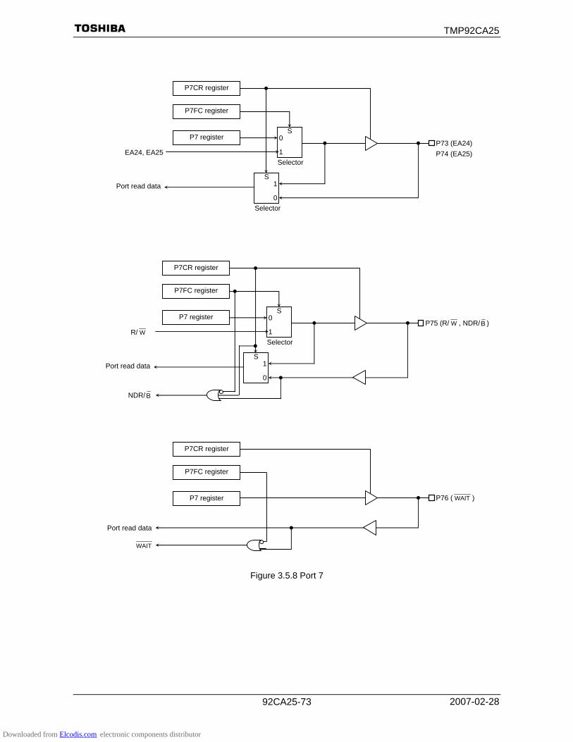
TMP92CA25
2007-02-28 92CA25-73
Figure 3.5.8 Port 7
P7CR register
P7FC register
P7 register P76 ( WAIT )
WAIT
Port read data
P7CR register
P7FC register
P7 register S
0
1
S1
0
P75 (R/ W , NDR/B )
Selector
Port read data
NDR/B
R/ W
P7CR register
P7FC register
P7 register S
0
1
S1
0
P73 (EA24) P74 (EA25)
Selector
Port read data
EA24, EA25
Selector
Downloaded from Elcodis.com electronic components distributor
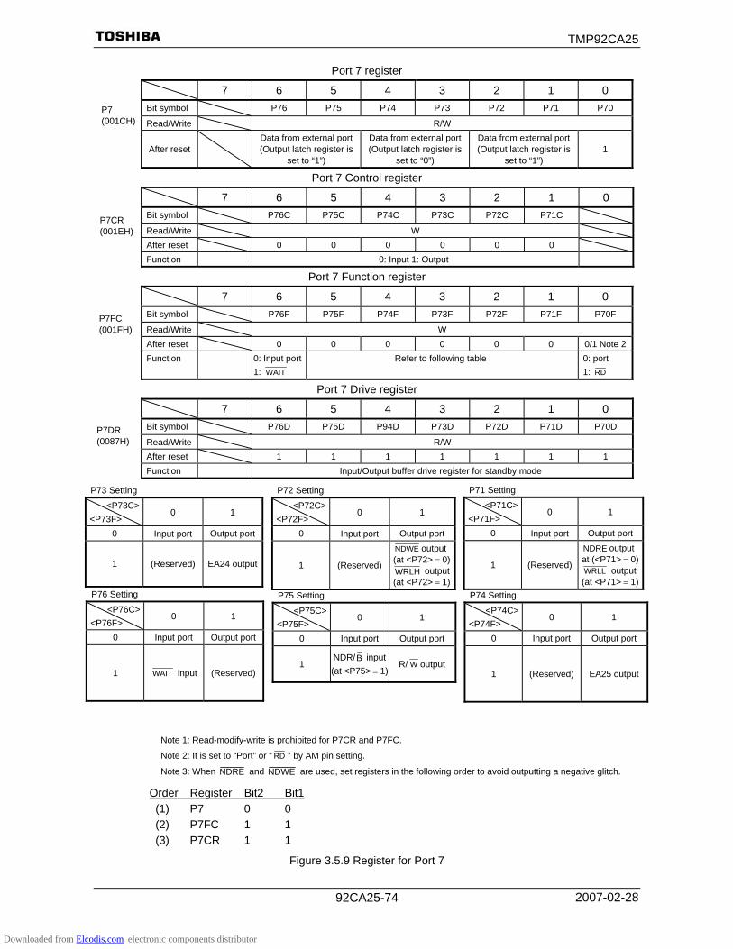
TMP92CA25
2007-02-28 92CA25-74
Port 7 register
7 6 5 4 3 2 1 0 Bit symbol P76 P75 P74 P73 P72 P71 P70
Read/Write R/W
After reset Data from external port
(Output latch register is set to “1”)
Data from external port (Output latch register is
set to “0”)
Data from external port (Output latch register is
set to “1”) 1
Port 7 Control register
7 6 5 4 3 2 1 0 Bit symbol P76C P75C P74C P73C P72C P71C
Read/Write W After reset 0 0 0 0 0 0 Function 0: Input 1: Output
Port 7 Function register
7 6 5 4 3 2 1 0 Bit symbol P76F P75F P74F P73F P72F P71F P70F
Read/Write W After reset 0 0 0 0 0 0 0/1 Note 2Function 0: Input port
1: WAIT Refer to following table 0: port
1: RD
Port 7 Drive register
7 6 5 4 3 2 1 0 Bit symbol P76D P75D P94D P73D P72D P71D P70D
Read/Write R/W After reset 1 1 1 1 1 1 1 Function Input/Output buffer drive register for standby mode
Note 1: Read-modify-write is prohibited for P7CR and P7FC.
Note 2: It is set to “Port” or “ RD ” by AM pin setting.
Note 3: When NDRE and NDWE are used, set registers in the following order to avoid outputting a negative glitch.
Order Register Bit2 Bit1 (1) P7 0 0 (2) P7FC 1 1 (3) P7CR 1 1
Figure 3.5.9 Register for Port 7
P72 Setting
<P72C><P72F>
0 1
0 Input port Output port
1 (Reserved)
NDWE output(at <P72> = 0)WRLH output(at <P72> = 1)
P71 Setting
<P71C> <P71F>
0 1
0 Input port Output port
1 (Reserved)
NDRE outputat (<P71> = 0)WRLL output(at <P71> = 1)
P76 Setting
<P76C> <P76F>
0 1
0 Input port Output port
1 WAIT input (Reserved)
P75 Setting
<P75C><P75F>
0 1
0 Input port Output port
1 NDR/B input(at <P75> = 1)
R/ W output
P7 (001CH)
P7CR (001EH)
P7FC (001FH)
P7DR (0087H)
P73 Setting
<P73C> <P73F>
0 1
0 Input port Output port
1 (Reserved) EA24 output
P74 Setting
<P74C> <P74F>
0 1
0 Input port Output port
1 (Reserved) EA25 output
Downloaded from Elcodis.com electronic components distributor
TMP92CA25
2007-02-28 92CA25-75
3.5.6 Port 8 (P80 to P87)
Ports 80 to 87 are 8-bit output ports. Resetting sets the output latch of P82 to “0” and the output latches of P80 to P81, P83 to P87 to “1”.
Port 8 can also be set to function as an interface pin for external memory using function register P8FC.
Writing “1” in the corresponding bit of P8FC and P8FC2 enables the respective functions. Resetting <P80F> to <P87F> of P8FC to “0” and P8FC2 to “0”, sets all bits to output
ports.
Figure 3.5.10 Port 8
Inte
rnal
dat
a bu
s
Function
control 2
Reset
P8FC2 write
Ouptut latch
P8 write
Selector
P8 read
P80 ( CS0 ) P81 ( CS1 , SDCS ) P82 ( CS2 , CSZA ) P83 ( CS3 ) P84 ( CSZB , CE0ND ) P85 ( CSZC , CE1ND ) P86 ( CSZD ) P87 ( CSZE )
Function
contol
P8FC write
“1”, “1”, “1”, “1”, CE0ND , CE1ND , “1”, “1”,
CS0 , CS1 , CS2 , CS3 , CSZB , CSZC , CSZD , CSZE
“1”, SDCS , CSZA , “1”
Downloaded from Elcodis.com electronic components distributor

TMP92CA25
2007-02-28 92CA25-76
Port 8 Register 7 6 5 4 3 2 1 0
Bit symbol P87 P86 P85 P84 P83 P82 P81 P80 P8 (0020H) Read/Write R/W
After reset 1 1 1 1 1 0 1 1
Port 8 Function Register 7 6 5 4 3 2 1 0
Bit symbol P87F P86F P85F P84F P83F P82F P81F P80F P8FC (0023H) Read/Write W
After reset 0 0 0 0 0 0 0 0 Function 0: Port
1: CSZE 0: Port 1: CSZD
Refer to following table
Refer to following table
0: Port 1: 3CS
Refer to following table
0: Port 1: 1CS
0: Port 1: 0CS
Port 8 Function Register 2 7 6 5 4 3 2 1 0
Bit symbol P87F2 P86F2 P85F2 P84F2 P83F2 P82F2 P81F2 P80F2 P8FC2 (0021H) Read/Write W
After reset 0 0 0 0 0 0 0 0 Function 0: <P87F>
1:Reserved 0: <P86F> 1:Reserved
Refer to following table
Refer to following table
Always write “0”
Refer to table below
0: <P81F> 1: SDCS
Always write “0”
Port 8 Drive Register 7 6 5 4 3 2 1 0
Bit symbol P87D P86D P85D P84D P83D P82D P81D P80D P8DR (0088H) Read/Write R/W
After reset 1 1 1 1 1 1 1 1 Function Input/Output buffer drive register for standby mode
Note 1: Read-modify-write is prohibited for P8FC and P8FC2. Note 2: Don’t write “1” to P8<P82> register before setting P82 pin to 2CS or CSZA because P82 pin output “0” as
CE for program memory by reset.
Figure 3.5.11 Register for Port 8
P85 Setting
<P85F> <P85F2>
0 1
0 Output port CSZC output 1 (Reserved) ND1CE output
P84 Setting
<P84F> <P84F2>
0 1
0 Output port CSZB output1 (Reserved) ND0CE output
P82 Setting
<P82F> <P82F2>
0 1
0 Output port 2CS output1 CSZA output Reserved
Downloaded from Elcodis.com electronic components distributor
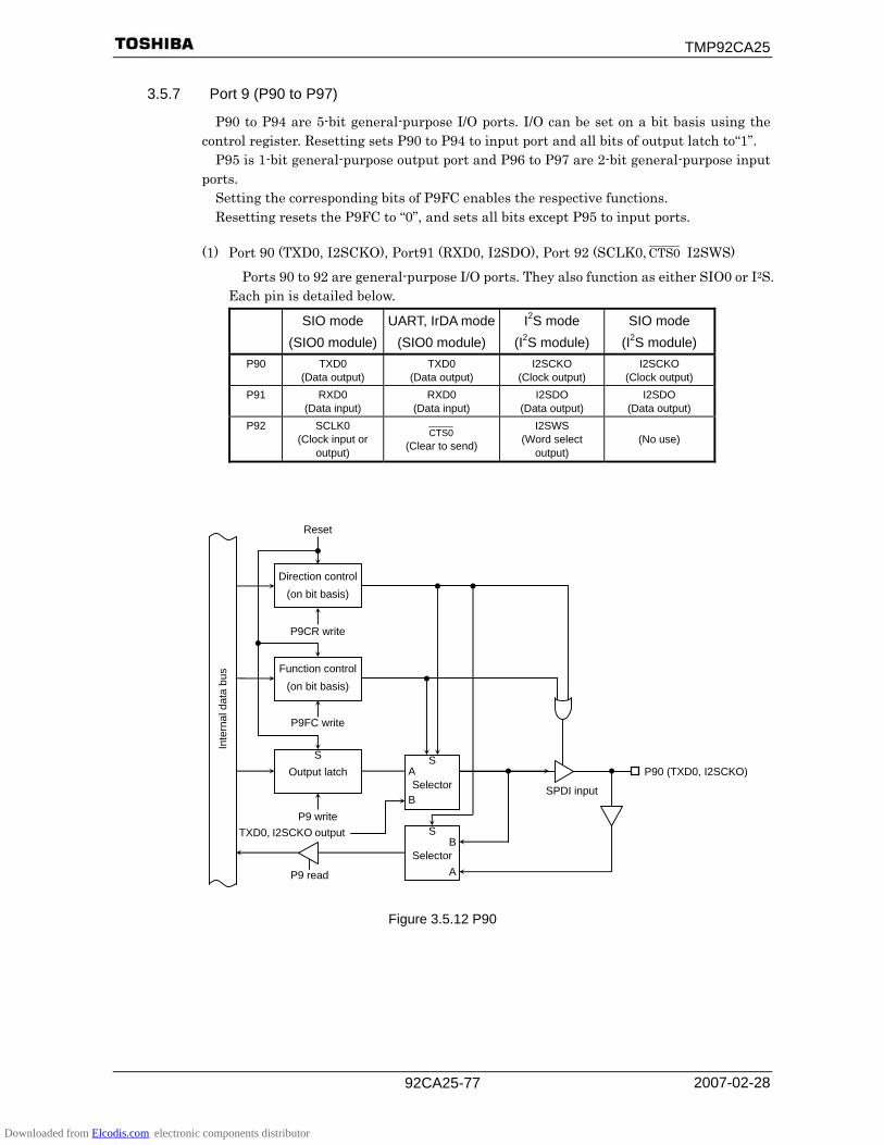
TMP92CA25
2007-02-28 92CA25-77
3.5.7 Port 9 (P90 to P97)
P90 to P94 are 5-bit general-purpose I/O ports. I/O can be set on a bit basis using the control register. Resetting sets P90 to P94 to input port and all bits of output latch to“1”.
P95 is 1-bit general-purpose output port and P96 to P97 are 2-bit general-purpose input ports.
Setting the corresponding bits of P9FC enables the respective functions. Resetting resets the P9FC to “0”, and sets all bits except P95 to input ports.
(1) Port 90 (TXD0, I2SCKO), Port91 (RXD0, I2SDO), Port 92 (SCLK0, CTS0 I2SWS)
Ports 90 to 92 are general-purpose I/O ports. They also function as either SIO0 or I2S. Each pin is detailed below.
SIO mode (SIO0 module)
UART, IrDA mode(SIO0 module)
I2S mode (I2S module)
SIO mode (I2S module)
P90 TXD0 (Data output)
TXD0 (Data output)
I2SCKO (Clock output)
I2SCKO (Clock output)
P91 RXD0 (Data input)
RXD0 (Data input)
I2SDO (Data output)
I2SDO (Data output)
P92 SCLK0 (Clock input or
output)
0CTS (Clear to send)
I2SWS (Word select
output) (No use)
Figure 3.5.12 P90
Inte
rnal
dat
a bu
s
Direction control (on bit basis)
Reset
P9CR write
P9 write
P9 read
P90 (TXD0, I2SCKO)
Function control (on bit basis)
P9FC write
TXD0, I2SCKO output
S Output latch
SB
SelectorA
SA Selector
B SPDI input
Downloaded from Elcodis.com electronic components distributor

TMP92CA25
2007-02-28 92CA25-78
Figure 3.5.13 P91 and P92
(2) P93 (SDA), P94 (SCL)
Figure 3.5.14 Port 93 and 94
Inte
rnal
dat
a bu
s
Direction control (on bit basis)
Reset
P9CR write
P9 write
P9 read
P91 (RXD0, I2SDO) P92 (SCLK0, 0CTS , I2SWS)
Function control (on bit basis)
P9FC write
I2SDO outputSCLK0,I2SWS output
S Output latch
SB
SelectorA
SA Selector
B
(to Port F1) P91RXD0 input(to Port F2) P92SCLK0 input
Inte
rnal
dat
a bu
s
Direction control (on bit basis)
Reset
P9CR write
P9 write
P9 read
P93(SDA), P94(SCL)
Function control (on bit basis)
P9FC write
SDA, SCL output
S Output latch
SB
SelectorA
SA Selector
B
Open drain enable P9FC2<P93F2, P94F2>
SDA, SCL input
Downloaded from Elcodis.com electronic components distributor

TMP92CA25
2007-02-28 92CA25-79
(3) P95 (CLK32KO)
Figure 3.5.15 Port 95
(4) P96 (INT4, PX), P97 (INT5, PY)
Figure 3.5.16 Port 96, 97
Inte
rnal
dat
a bu
s Reset
P9 read
P96 (INT4, PX)P97 (INT5, PY)
Function control
P9FC write
INT4 INT5
SA
SelectorB
Rising/Falling edge detection
TSICR1<DBC7>
De-bounce circuit
TSICR0<TWIEN, TSI7>
TSICR0<PXEN><PYEN>
TSICR0<TSI7>
TSICR0<PXEN>TSICR0<TSI7>
IIMC<I4EDGE, I5EDGE>
Pull-down resistor typ.200kΩ
Only for P96
AVCC
Switch for TSI Typ.20Ω
Inte
rnal
dat
a bu
s
Direction control (on bit basis)
Reset
P9CR write
P9 write
P9 read
P95 (CLK32KO)
Funtcion control (on bit basis)
P9FC write
fs
S Output latch
SA Selector
B
Downloaded from Elcodis.com electronic components distributor
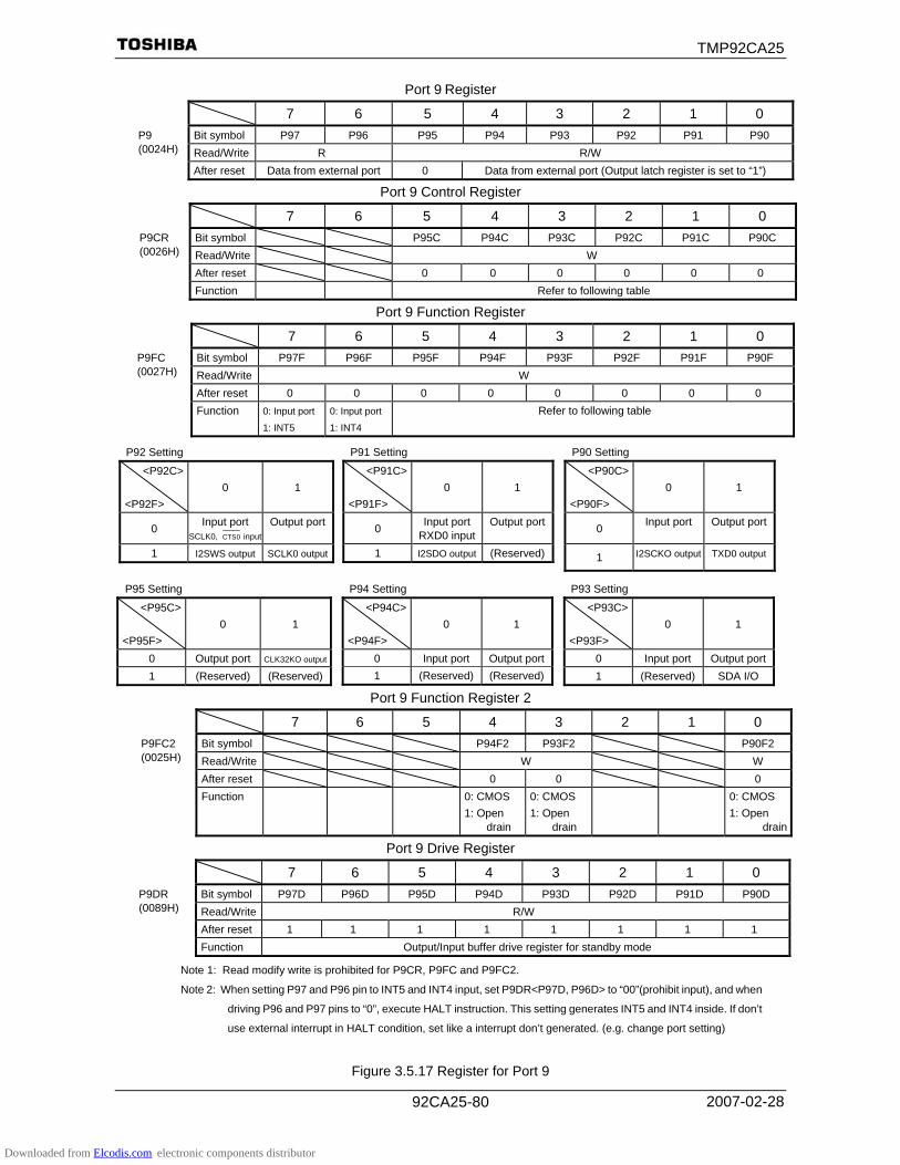
TMP92CA25
2007-02-28 92CA25-80
Port 9 Register 7 6 5 4 3 2 1 0
Bit symbol P97 P96 P95 P94 P93 P92 P91 P90 P9 (0024H) Read/Write R R/W
After reset Data from external port 0 Data from external port (Output latch register is set to “1”)
Port 9 Control Register 7 6 5 4 3 2 1 0
Bit symbol P95C P94C P93C P92C P91C P90C P9CR (0026H) Read/Write W
After reset 0 0 0 0 0 0 Function Refer to following table
Port 9 Function Register 7 6 5 4 3 2 1 0
Bit symbol P97F P96F P95F P94F P93F P92F P91F P90F P9FC (0027H) Read/Write W
After reset 0 0 0 0 0 0 0 0 Function 0: Input port
1: INT5
0: Input port
1: INT4
Refer to following table
Port 9 Function Register 2 7 6 5 4 3 2 1 0
Bit symbol P94F2 P93F2 P90F2 P9FC2 (0025H) Read/Write W W
After reset 0 0 0 Function 0: CMOS
1: Open drain
0: CMOS 1: Open
drain
0: CMOS 1: Open
drain
Port 9 Drive Register 7 6 5 4 3 2 1 0
Bit symbol P97D P96D P95D P94D P93D P92D P91D P90D P9DR (0089H) Read/Write R/W
After reset 1 1 1 1 1 1 1 1 Function Output/Input buffer drive register for standby mode
Note 1: Read modify write is prohibited for P9CR, P9FC and P9FC2.
Note 2: When setting P97 and P96 pin to INT5 and INT4 input, set P9DR<P97D, P96D> to “00”(prohibit input), and when
driving P96 and P97 pins to “0”, execute HALT instruction. This setting generates INT5 and INT4 inside. If don’t
use external interrupt in HALT condition, set like a interrupt don’t generated. (e.g. change port setting)
Figure 3.5.17 Register for Port 9
P92 Setting
<P92C> <P92F>
0 1
0 Input port SCLK0, 0CTS input
Output port
1 I2SWS output SCLK0 output
P91 Setting
<P91C> <P91F>
0 1
0 Input portRXD0 input
Output port
1 I2SDO output (Reserved)
P90 Setting
<P90C> <P90F>
0 1
0 Input port Output port
1 I2SCKO output TXD0 output
P95 Setting
<P95C> <P95F>
0 1
0 Output port CLK32KO output
1 (Reserved) (Reserved)
P94 Setting
<P94C> <P94F>
0 1
0 Input port Output port1 (Reserved) (Reserved)
P93 Setting
<P93C> <P93F>
0 1
0 Input port Output port1 (Reserved) SDA I/O
Downloaded from Elcodis.com electronic components distributor

TMP92CA25
2007-02-28 92CA25-81
3.5.8 Port A (PA0 to PA7)
Ports A0 to A7 are 8-bit input general-purpose ports with pull-up resistor. In addition to functioning as general-purpose I/O ports, ports A0 to A7 can also, as a keyboard interface, operate a key-on wakeup function. The various functions can each be enabled by writing a “1” to the corresponding bit of the port A function register (PAFC).
Resetting resets all bits of the register PAFC to “0” and sets all pins to be input port.
Figure 3.5.18 Port A
When PAFC = “1”, if the input of any of KI0 to KI7 pins fall down, an INTKEY interrupt is generated. An INTKEY interrupt can be used to release all HALT modes.
Inte
rnal
dat
a bu
s
PA0 (KI0) PA1 (KI1) PA2 (KI2) PA3 (KI3) PA4 (KI4) PA5 (KI5) PA6 (KI6) PA7 (KI7)
INTKEY Edge
detection
Key-on Enable
(on bit basis)
PAFC write
PA read
Pull-up resistor
Reset
PA0 to PA7 8-input OR
Downloaded from Elcodis.com electronic components distributor

TMP92CA25
2007-02-28 92CA25-82
Port A Register
7 6 5 4 3 2 1 0 Bit symbol PA7 PA6 PA5 PA4 PA3 PA2 PA1 PA0
Read/Write R/W After reset Data from external port
Port A Function Register
7 6 5 4 3 2 1 0 Bit symbol PA7F PA6F PA5F PA4F PA3F PA2F PA1F PA0F
Read/Write W After reset 0 0 0 0 0 0 0 0 Function 0: Key input disable 1: Key input enable
Port A Drive register
7 6 5 4 3 2 1 0 Bit symbol PA7D PA6D PA5D PA4D PA3D PA2D PA1D PA0D
Read/Write W After reset 1 1 1 1 1 1 1 1 Function Input/Output buffer drive register for standby mode
Note: Read-modify-write is prohibited for PACR and PAFC.
Figure 3.5.19 Register for Port A
PADR (008AH)
PA (0028H)
PAFC (002BH)
Downloaded from Elcodis.com electronic components distributor

TMP92CA25
2007-02-28 92CA25-83
3.5.9 Port C (PC0 to PC3, PC6 to PC7)
PC0 to PC7 are 8-bit general-purpose I/O ports. Each bit can be set individually for input or output. Resetting sets port C to an input port.
In addition to functioning as a general-purpose I/O port, port C can also function as an output pin for timers (TA1OUT, TA3OUT and TB0OUT0), input pin for external interruption (INT0 to INT3), output pin for memory ( CSZF ), output pin for key (KO8). These settings are made using the function register PCFC. The edge select for external interruption is determined by the IIMC register in the interruption controller.
(1) PC0 (INT0, TA1OUT)
Figure 3.5.20 Port C0
Inte
rnal
dat
a bu
s
Direction control
Reset
PCCR write
PC read
PC0 (INT0,TA1OUT)
PC write
SOutput latch
SB
SelectorA
Function control
PCFC write
INT0
SA Selector
B
IIMC<I0LE, I0EDGE>
TA1OUT
Level/edge select and
Rising/falling select
Inte
rnal
dat
a bu
s
Direction control(on bit basis)
Reset
PCCR write
PC read
PC0 (INT0,TA1OUT)
PC write
SOutput latch
SB
SelectorA
Function control(on bit basis)
PCFC write
INT0
SA Selector
B
IIMC<I0LE, I0EDGE>
TA1OUT
Level/edge select and
Rising/falling select
Downloaded from Elcodis.com electronic components distributor

TMP92CA25
2007-02-28 92CA25-84
(2) PC1 (INT1, TA3OUT), PC2 (INT2, TB0OUT0), PC3 (INT3, TB0OUT1)
Figure 3.5.21 Port C1, C2, C3
(3) PC4, PC5
Figure 3.5.22 Port C4, C5
Inte
rnal
dat
a bu
s
Direction control (on bit basis)
Reset
PCCR write
PC read
PC1 (INT1, TA3OUT)PC2 (INT2, TB0OUT0)PC3 (INT3)
PC write
S Output latch
SB
SelectorA
PCFC write
INT1 to
INT3
SA Selector
B
Rising/falling edge detection
IIMC<I1EDGE, I2EDGE, I3EDGE >
TA3OUTTB0OUT0
Function control (on bit basis)
Inte
rnal
dat
a bu
s
Direction control(on bit basis)
Reset
PCCR write
PC write
PC read
PC4 PC5
PCFC write
S Output latch
SB
SelectorA
Function control(on bit basis)
Downloaded from Elcodis.com electronic components distributor

TMP92CA25
2007-02-28 92CA25-85
(4) PC6 (KO8, EA24)
Figure 3.5.23 Port C6
(4) PC7 ( CSZF , EA25)
Figure 3.5.24 Port C7
SA Selector
B C
Inte
rnal
dat
a bu
s
Direction control(on bit basis)
Reset
PCCR write
PC read
PC7 ( CSZF , EA25)
PC write
S Output latch
SB
SelectorA
Funtcion control(on bit basis)
PFFC write
CSZFEA25
In
tern
al d
ata
bus
Direction control(on bit basis)
Reset
PCCR write
PC read
PC6 (KO8, EA24)
PC write
S Output latch
SB
SelectorA
Funtcion control(on bit basis)
PCFC write
SA Selector
B
EA24
Open drainenable
Downloaded from Elcodis.com electronic components distributor

TMP92CA25
2007-02-28 92CA25-86
Port C Register 7 6 5 4 3 2 1 0
Bit symbol PC7 PC6 PC5 PC4 PC3 PC2 PC1 PC0 PC (0030H) Read/Write R/W
After reset Data from external port (Output latch register is set to “1”)
Port C Control Register 7 6 5 4 3 2 1 0
Bit symbol PC7C PC6C PC5C PC4C PC3C PC2C PC1C PC0C PCCR (0032H) Read/Write W
After reset 0 0 0 0 0 0 0 0 Function Refer to following table
Port C Function Register 7 6 5 4 3 2 1 0
Bit symbol PC7F PC6F PC5F PC4F PC3F PC2F PC1F PC0F PCFC (0033H) Read/Write W
After reset 0 0 0 0 0 0 0 0 Function Refer to following table
Port C Drive Register 7 6 5 4 3 2 1 0
Bit symbol PC7D PC6D PC5D PC4D PC3D PC2D PC1D PC0D Read/Write R/W
After reset 1 1 1 1 1 1 1 1 Function Input/Output buffer drive register for standby mode
Note1: Read-modify-write is prohibited for the registers PCCR and PCFC.
Note2: When setting PC3-PC0 pins to INT3-INT0 input, set PCDR<PC3D:PC0D> to “0000”(prohibit input), and when
driving PC3-PC0 pins to “0”, execute HALT instruction. This setting generates INT3-INT0 inside. If don’t use
external interrupt in HALT condition, set like an interrupt don’t generated. (e.g. change port setting)
Figure 3.5.25 Register for Port C
PC2 Setting
<PC2C> <PC2F>
0 1
0 Input port Output port 1 INT2 TB0OUT
PC1 Setting
<PC1C><PC1F>
0 1
0 Input port Output port1 INT1 TA3OUT
PC0 Setting
<PC0C> <PC0F>
0 1
0 Input port Output port1 INT0 TA1OUT
PC5 Setting
<PC5C> <PC5F>
0 1
0 Input port Output port 1 (Reserved) (Reserved)
PC4 Setting
<PC4C><PC4F>
0 1
0 Input port Output port1 (Reserved) (Reserved)
PC3 Setting
<PC3C> <PC3F>
0 1
0 Input port Output port1 INT3 (Reserved)
PCDR (008CH)
PC6 Setting <PC6C>
<PC6F>
0 1
0 Input port Output port
1 KO8
(Open drain) EA24 output at <PC6>= 0
PC7 Setting <PC7C>
<PC7F>
0 1
0 Input port Output port
1 CSZF I/O EA25 output
at <PC7>= 0
Downloaded from Elcodis.com electronic components distributor
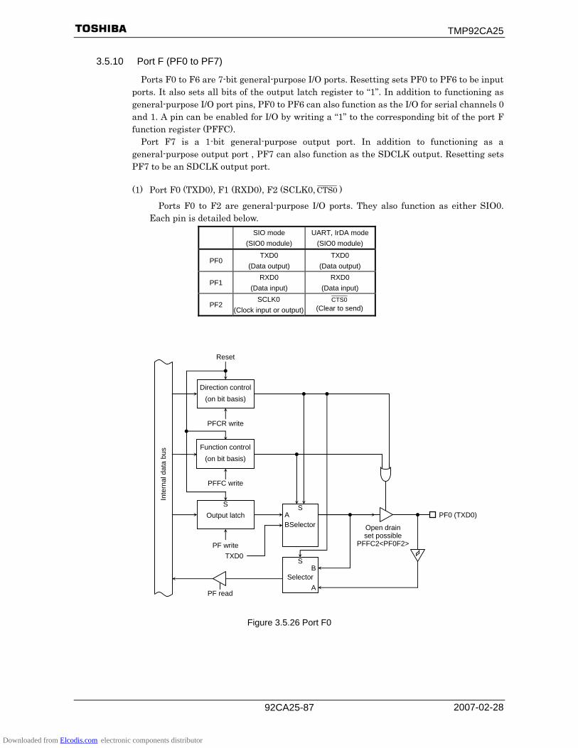
TMP92CA25
2007-02-28 92CA25-87
3.5.10 Port F (PF0 to PF7)
Ports F0 to F6 are 7-bit general-purpose I/O ports. Resetting sets PF0 to PF6 to be input ports. It also sets all bits of the output latch register to “1”. In addition to functioning as general-purpose I/O port pins, PF0 to PF6 can also function as the I/O for serial channels 0 and 1. A pin can be enabled for I/O by writing a “1” to the corresponding bit of the port F function register (PFFC).
Port F7 is a 1-bit general-purpose output port. In addition to functioning as a general-purpose output port , PF7 can also function as the SDCLK output. Resetting sets PF7 to be an SDCLK output port.
(1) Port F0 (TXD0), F1 (RXD0), F2 (SCLK0, CTS0 )
Ports F0 to F2 are general-purpose I/O ports. They also function as either SIO0. Each pin is detailed below.
SIO mode (SIO0 module)
UART, IrDA mode(SIO0 module)
PF0 TXD0
(Data output) TXD0
(Data output)
PF1 RXD0
(Data input) RXD0
(Data input)
PF2 SCLK0
(Clock input or output)0CTS
(Clear to send)
Figure 3.5.26 Port F0
Inte
rnal
dat
a bu
s
Direction control(on bit basis)
Reset
PFCR write
PF write
PF read
PF0 (TXD0)
PFFC write
TXD0
S Output latch
SB
SelectorA
SA BSelector
Open drain set possible
PFFC2<PF0F2>
Function control(on bit basis)
Downloaded from Elcodis.com electronic components distributor

TMP92CA25
2007-02-28 92CA25-88
Figure 3.5.27 Port F1
Figure 3.5.28 Port F2
Inte
rnal
dat
a bu
s
Direction control (on bit basis)
Reset
PFCR write
PF read
PF1 (RXD0)
PF write
S Output latch
SA
SelectorB
SB
SelectorA
PFFC<PF1F>
RXD0
P91RXD0 input
Inte
rnal
dat
a bu
s
Direction control (on bit basis)
Reset
PFCR write
PF read
PF2 (SCLK0, 0CTS )
PF write
S Output latch
SA
SelectorB
SB
SelectorA
SCLK0 input, 0CTS input
PFFC write
SelectorS SCLK0 output
P92SCLK0 input
Function control (on bit basis)
PFFC<PF2F>
Downloaded from Elcodis.com electronic components distributor

TMP92CA25
2007-02-28 92CA25-89
(2) PF3, PF4, PF5, PF6, PF7
Figure 3.5.29 Port F3, F4. F5 and F6
Figure 3.5.30 Port F7
Inte
rnal
dat
a bu
s
Direction control (on bit basis)
Reset
PFCR write
PF write
PF read
PF3 PF4 PF5 PF6
Function control (on bit basis)
PFFC write
S Output latch
SB
SelectorA
Inte
rnal
dat
a bu
s
Reset
PF read
PF7 (SDCLK)
PF write
S Output latch
Function control(on bit basis)
PFFC write
SA Selector
B SDCLK
Downloaded from Elcodis.com electronic components distributor

TMP92CA25
2007-02-28 92CA25-90
Port F Register
7 6 5 4 3 2 1 0 Bit symbol PF7 PF6 PF5 PF4 PF3 PF2 PF1 PF0 PF
(003CH) Read/Write R/W After reset 1 Data from external port (Output latch register is set to “1”)
Port F Control Register 7 6 5 4 3 2 1 0
Bit symbol PF6C PF5C PF4C PF3C PF2C PF1C PF0C PFCR (003EH) Read/Write W
After reset 0 0 0 0 0 0 0 Function Refer to following table
Port F Functon Register 7 6 5 4 3 2 1 0
Bit symbol PF7F PF6F PF5F PF4F PF3F PF2F PF1F PF0F PFFC (003FH) Read/Write W
After reset 1 0 0 0 0 0 0 0 Function Refer to following table RXD0 pin
selection 0: Port F1 1: Port 91
Refer to following table
PF2 Setting
<PF2C> <PF2F>
0 1
0
Input port,
SCLK0, 0CTS input From PF2 pin at <PF2> = 0
From P92 pin at <PF2> = 1
Output port
1 (Reserved) SCLK0 output
PF1 Setting
<PF1C><PF1F>
0 1
0 Input port,
RXD0 input from PF1,
Output port
1
RXD0 input from P91 Reserved
PF0 Setting
<PF0C> <PF0F>
0 1
0 Input port Output port
1
(Reserved) TXD0 output
PF4 Setting
<PF4C><PF4F>
0 1
0 Input Output
1 (Reserved) (Reserved)
PF3 Setting
<PF3C> <PF3F>
0 1
0 Input port Output port
1 (Reserved) (Reserved)
PF5 Setting
<PF5C> <PF5F>
0 1
0 Input port Output port
1 (Reserved) (Reserved)
PF6 Setting
<PF6C><PF6F>
0 1
0 Input port Output port
1 (Reserved) (Reserved)
PF7 Setting
<PF7F>
0 Output port
1 SDCLK output
Downloaded from Elcodis.com electronic components distributor
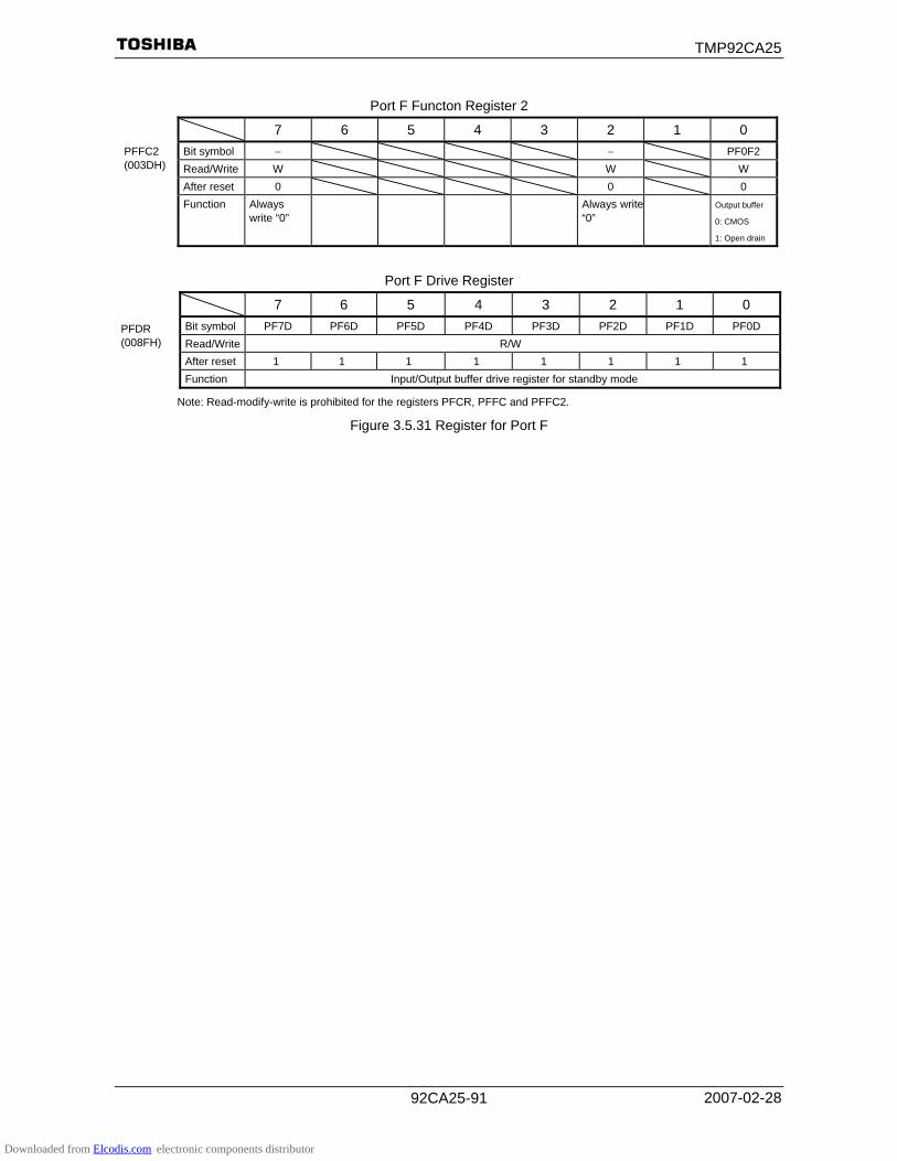
TMP92CA25
2007-02-28 92CA25-91
Port F Functon Register 2
7 6 5 4 3 2 1 0 Bit symbol − − PF0F2 PFFC2
(003DH) Read/Write W W W After reset 0 0 0 Function Always
write “0” Always write
“0” Output buffer
0: CMOS
1: Open drain
Port F Drive Register
7 6 5 4 3 2 1 0 Bit symbol PF7D PF6D PF5D PF4D PF3D PF2D PF1D PF0D Read/Write R/W
After reset 1 1 1 1 1 1 1 1 Function Input/Output buffer drive register for standby mode
Note: Read-modify-write is prohibited for the registers PFCR, PFFC and PFFC2.
Figure 3.5.31 Register for Port F
PFDR (008FH)
Downloaded from Elcodis.com electronic components distributor

TMP92CA25
2007-02-28 92CA25-92
3.5.11 Port G (PG0 to PG3)
PG0 to PG3 are 4-bit input ports and can also be used as the analog input pins for the internal AD converter. PG3 can also be used as the ADTRG pin for the AD converter.
PG2 and PG3 can also be used as the MX and MY pins for a touch screen interface.
Figure 3.5.32 Port G
Port G Register 7 6 5 4 3 2 1 0
Bit symbol PG2 PG2 PG1 PG0 PG (0040H) Read/Write R
After reset Data from external port
Note: The input channel selection of the AD converter and the permission for ADTRG input are set by AD converter mode
register ADMOD1.
Port G Drive Register 7 6 5 4 3 2 1 0
Bit symbol PG3D PG2D PGDR (0090H) Read/Write R/W
After reset 1 1 Function Input/Output buffer drive
register for standby mode
Figure 3.5.33 Register for Port G
Inte
rnal
dat
a bu
s
ADTRG (only for PG3)
Port G read
PG0 (AN0), PG1 (AN1), PG2 (AN2, MX), PG3 (AN3, MY, ADTRG )
AD converter
Channelselector
AD read
Conversionresult
register
TSICR0<MXEN, MYEN>
TSICR0<TSI7>
(Only for PG2, PG3)
Switch for TSItyp. 20Ω
Downloaded from Elcodis.com electronic components distributor

TMP92CA25
2007-02-28 92CA25-93
3.5.12 Port J (PJ0 to PJ7)
PJ0 to PJ4 and PJ7 are 6-bit output ports. Resetting sets the output latch PJ to “1”, and they output “1”. PJ5 to PJ6 are 2-bit I/O ports.
In addition to functioning as a port, port J also functions as output pins for SDRAM ( SDRAS , SDCAS , SDWE , SDLLDQM, SDLUDQM and SDCKE), SRAM ( SRWR , SRLLB , SRLUB ) and NAND flash (NDALE and NDCLE).
The above settings are made using the function register PJFC. However, H either SDRAM or SRAM output signals for PJ0 to PJ2 are selected
automatically according to the setting of the memory controller.
Figure 3.5.34 Port J0, J1, J2, J3, J4 and J7
Inte
rnal
dat
a bu
s
Function control 2(on bit basis)
Reset
PJFC2 write
PJ write
PJ read
PJ0 ( SDRAS , SRLLB ) PJ1 ( SDCAS , SRLUB ) PJ2 ( SDWE , SRWR ) PJ3 (SDLLDQM) PJ4 (SDLUDQM) PJ7 (SDCKE)
Function control (on bit basis)
PJFC write
Output latch
S
Selector
SRLLB , SRLUB , SRWR SDRAS , SDCAS , SDWE , SDLLDQM, SDLUDQM, SDCKE
Downloaded from Elcodis.com electronic components distributor
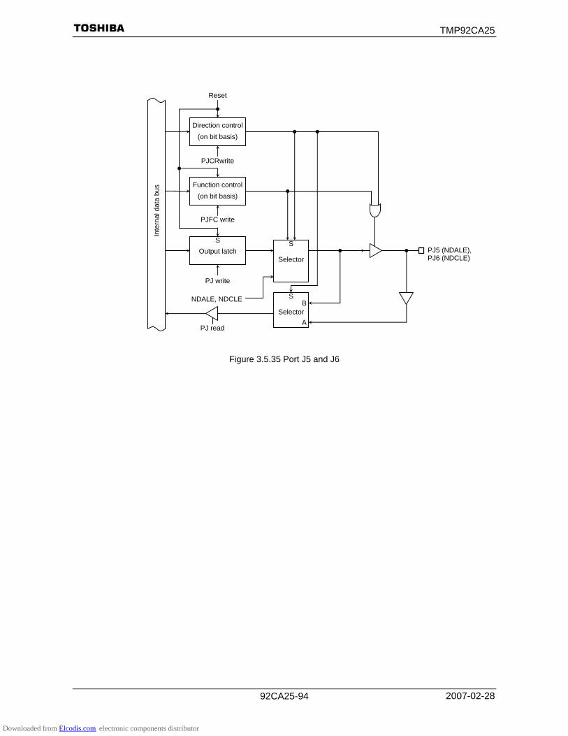
TMP92CA25
2007-02-28 92CA25-94
Figure 3.5.35 Port J5 and J6
PJ5 (NDALE), PJ6 (NDCLE)
Inte
rnal
dat
a bu
s
Direction control(on bit basis)
Reset
PJCRwrite
PJ write
PJ read
Function control (on bit basis)
PJFC write
NDALE, NDCLE
S Output latch
SB
SelectorA
S Selector
Downloaded from Elcodis.com electronic components distributor
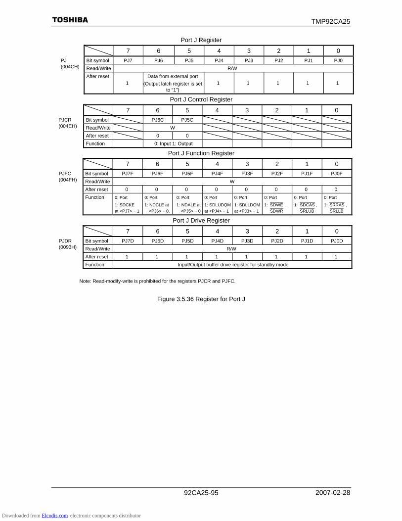
TMP92CA25
2007-02-28 92CA25-95
Port J Register 7 6 5 4 3 2 1 0
Bit symbol PJ7 PJ6 PJ5 PJ4 PJ3 PJ2 PJ1 PJ0 PJ (004CH) Read/Write R/W
After reset 1
Data from external port (Output latch register is set
to “1”) 1 1 1 1 1
Port J Control Register 7 6 5 4 3 2 1 0
Bit symbol PJ6C PJ5C PJCR (004EH) Read/Write W
After reset 0 0 Function 0: Input 1: Output
Port J Function Register 7 6 5 4 3 2 1 0
Bit symbol PJ7F PJ6F PJ5F PJ4F PJ3F PJ2F PJ1F PJ0F PJFC (004FH) Read/Write W
After reset 0 0 0 0 0 0 0 0 Function 0: Port
1: SDCKE at <PJ7> = 1
0: Port
1: NDCLE at <PJ6> = 0,
0: Port
1: NDALE at<PJ5> = 0
0: Port
1: SDLUDQM at <PJ4> = 1
0: Port
1: SDLLDQM at <PJ3> = 1
0: Port
1: SDWE , SDWR
0: Port
1: SDCAS , SRLUB
0: Port
1: SRRAS , SRLLB
Port J Drive Register 7 6 5 4 3 2 1 0
Bit symbol PJ7D PJ6D PJ5D PJ4D PJ3D PJ2D PJ1D PJ0D PJDR (0093H) Read/Write R/W
After reset 1 1 1 1 1 1 1 1 Function Input/Output buffer drive register for standby mode
Note: Read-modify-write is prohibited for the registers PJCR and PJFC.
Figure 3.5.36 Register for Port J
Downloaded from Elcodis.com electronic components distributor

TMP92CA25
2007-02-28 92CA25-96
3.5.13 Port K (PK0 to PK7)
Port K is a 4-bit output port. Resetting sets the output latch PK to “0”, and PK0 to PK3 pins output “0”.
PK4 to PK7 are 4-bit input ports. Resetting sets the PLCR to “0”, and set input port. In addition to functioning as an output port, port K also functions as output pins for an
LCD controller (LCP0, LLP, LFR and LBCD) and pin for an SPI controller (SPCLK, SPCS , SPDO and SPDI).
The above settings are made using the function register PKFC.
Figure 3.5.37 Port K0 to K3
Inte
rnal
dat
a bu
s
Reset
Output latch
PK write
SA
Selector
B
PK read
PK0 (LCP0) PK1(LLP) PK2 (LFR) PK3 (LBCD)
Function control (on bit basis)
PKFC write
Output buffer
LCP0, LLP, LFR, LBCD
Downloaded from Elcodis.com electronic components distributor

TMP92CA25
2007-02-28 92CA25-97
Figure 3.5.38 Port K4
Figure 3.5.39 Port K5 to K7
Inte
rnal
dat
a bu
s
Direction contorl (on bit basis)
Reset
PKCR write
PK write
PK read
PK4 (SPDI)
Function control(on bit basis)
PKFC write
S Output latch
SB
SelectorA
Inte
rnal
dat
a bu
s
Reset
PKCR write
PK write
PJ read
PK5 (SPDO)PK6 ( SPCS )PK7 (SPCLK)
Function control(on bit basis)
PKFC write
S Output latch
SB
SelectorA
SA
SelectorB
SPDOSPCSSPCLK
SPDI input
Direction control(on bit basis)
Downloaded from Elcodis.com electronic components distributor

TMP92CA25
2007-02-28 92CA25-98
Port K Register
7 6 5 4 3 2 1 0 Bit symbol PK7 PK6 PK5 PK4 PK3 PK2 PK1 PK0 PK
(0050H) Read/Write R/W After reset Data from external port
(Output latch register is cleared to “0”) 0 0 0 0
Port K Control Register 7 6 5 4 3 2 1 0
Bit symbol PK7C PK6C PK5C PK4C PKCR (0052H) Read/Write W
After reset 0 0 0 0 Function 0: Input 1: Output
Port K Function Register 7 6 5 4 3 2 1 0
Bit symbol PK7F PK6F PK5F PK4F PK3F PK2F PK1F PK0F PKFC (0053H) Read/Write W
After reset 0 0 0 0 0 0 0 0 Function 0: Port
1: SPCLK output
0: Port 1: SPCS
output
0: Port 1: SPDO
output
0: Port 1: SPDI
output
0: Port 1: LBCD
0: Port 1: LFR
0: Port 1: LLP
0: Port 1: LCP0
Port K Drive Register 7 6 5 4 3 2 1 0
Bit symbol PK7D PK6D PK5D PK4D PK3D PK2D PK1D PK0D PKDR (0094H) Read/Write R/W
After reset 1 1 1 1 1 1 1 1 Function Input/Output buffer drive register for standby mode
Note: Read-modify-write is prohibited for the register PKFC.
Figure 3.5.40 Register for Port K
PK5 Setting <PK5C>
<PK5F> 0 1
0 Input port Output port
1 Reserved SPDO output
PK4 Setting <PK4C>
<PK4F> 0 1
0 Input port Output port
1 SPDI input Reserved
PK7 Setting <PK7C>
<PK7F> 0 1
0 Input port Output port
1 Reserved SPCLK output
PK6 Setting <PK6C>
<PK6F> 0 1
0 Input port Output port
1 Reserved SPCS output
Downloaded from Elcodis.com electronic components distributor
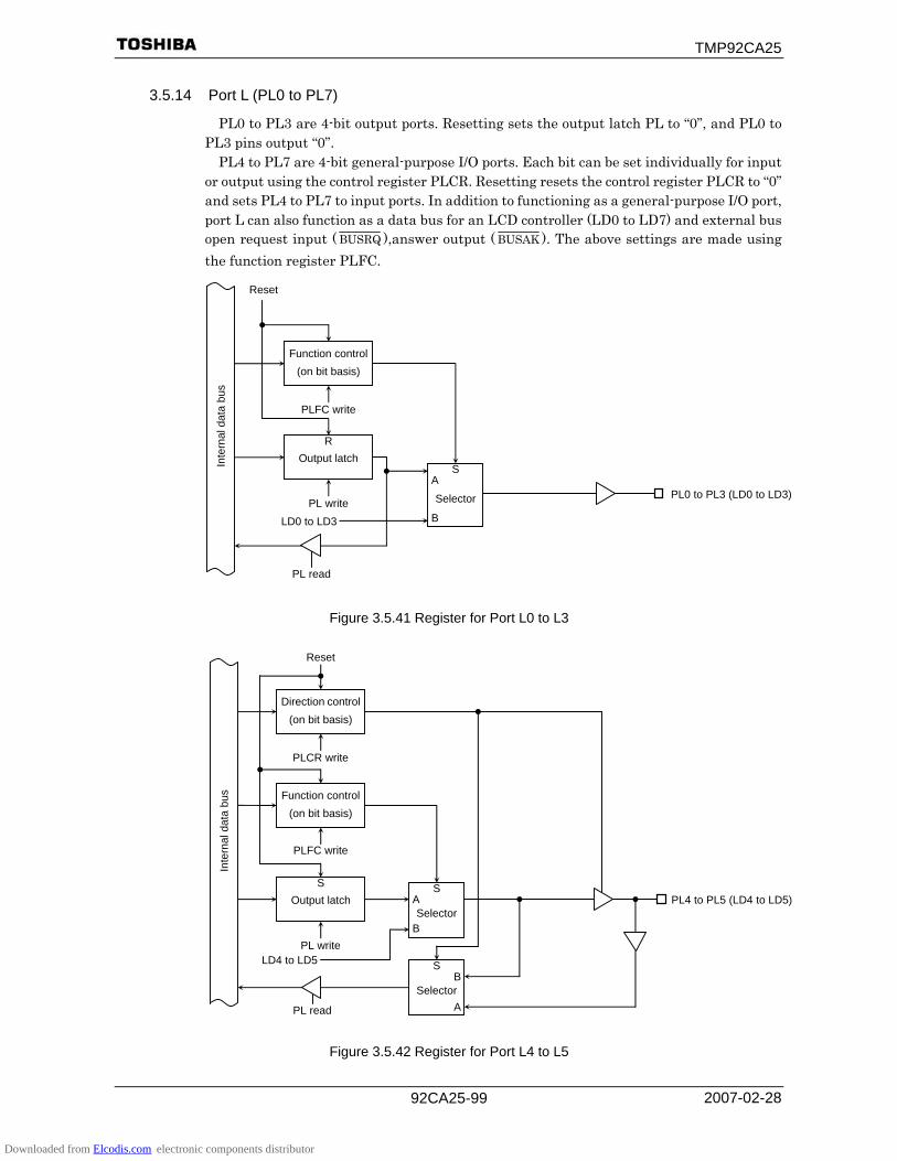
TMP92CA25
2007-02-28 92CA25-99
3.5.14 Port L (PL0 to PL7)
PL0 to PL3 are 4-bit output ports. Resetting sets the output latch PL to “0”, and PL0 to PL3 pins output “0”.
PL4 to PL7 are 4-bit general-purpose I/O ports. Each bit can be set individually for input or output using the control register PLCR. Resetting resets the control register PLCR to “0” and sets PL4 to PL7 to input ports. In addition to functioning as a general-purpose I/O port, port L can also function as a data bus for an LCD controller (LD0 to LD7) and external bus open request input ( BUSRQ ),answer output ( BUSAK ). The above settings are made using the function register PLFC.
Figure 3.5.41 Register for Port L0 to L3
Figure 3.5.42 Register for Port L4 to L5
Inte
rnal
dat
a bu
s
Direction control (on bit basis)
Reset
PLCR write
PL write
PL read
PL4 to PL5 (LD4 to LD5)
Function control (on bit basis)
PLFC write
S Output latch
SB
SelectorA
SA Selector
B
LD4 to LD5
Inte
rnal
dat
a bu
s
Reset
R Output latch
PL write
SA
Selector
B
PL read
PL0 to PL3 (LD0 to LD3)
Function control (on bit basis)
PLFC write
LD0 to LD3
Downloaded from Elcodis.com electronic components distributor
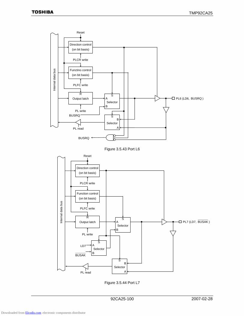
TMP92CA25
2007-02-28 92CA25-100
Figure 3.5.43 Port L6
Figure 3.5.44 Port L7
Inte
rnal
dat
a bu
s
Direction control (on bit basis)
Reset
PLCR write
PL write
PL read
PL6 (LD6, BUSRQ )
Functino control (on bit basis)
PLFC write
R Output latch
SB
SelectorA
SA Selector
B
BUSRQ
Inte
rnal
dat
a bu
s
Direction control (on bit basis)
Reset
PLCR write
PL write
PL read
PL7 (LD7, BUSAK )
Function control (on bit basis)
PLFC write
R Output latch
SB
SelectorA
SA Selector
B
S A Selector
B
LD7
BUSAK
BUSRQ
Downloaded from Elcodis.com electronic components distributor

TMP92CA25
2007-02-28 92CA25-101
Port L Register 7 6 5 4 3 2 1 0
Bit symbol PL7 PL6 PL5 PL4 PL3 PL2 PL1 PL0 PL (0054H) Read/Write R/W
After reset Data from external port (Output latch register is cleared to “0”)
0 0 0 0
Port L Control Register 7 6 5 4 3 2 1 0
Bit symbol PL7C PL6C PL5C PL4C PLCR (0056H) Read/Write W
After reset 0 0 0 0 Function 0: Input 1: Output
Port L Function Register 7 6 5 4 3 2 1 0
Bit symbol PL7F PL6F PL5F PL4F PL3F PL2F PL1F PL0F PLFC (0057H) Read/Write W
After reset 0 0 0 0 0 0 0 0 Function Refer following table 0: Port 1: Data bus for LCDC (LD3 to LD0)
Port L Drive Register 7 6 5 4 3 2 1 0
Bit symbol PL7D PL6D PL5D PL4D PL3D PL2D PL1D PL0D PLDR (0095H) Read/Write R/W
After reset 1 1 1 1 1 1 1 1 Function Input/Output buffer drive register for standby mode
Note1: Read-modify-write is prohibited for the registers PLCR and PLFC. Note2: When Port L are used at LD0 to LD7, If set PL6 pin to BUSRQ function input temporarily, CPU may not be
operate normally. Therefore, set registers by following order.
Order Register Setting value
(1) PLCR 1
(2) PLFC 1
Figure 3.5.45 Port L Register
PL5 Setting <PL5C>
<PL5F> 0 1
0 Input port Output port
1 Reserved LD5 output
PL4 Setting <PL4C>
<PL4F> 0 1
0 Input port Output port
1 Reserved LD4 output
PL7 Setting
<PL7C><PL7F> 0 1
0 Input port Output port1 BUSAK output LD7 output
PL6 Setting <PL6C>
<PL6F> 0 1
0 Input port Output port1 BUSRQ input LD6 output
Downloaded from Elcodis.com electronic components distributor
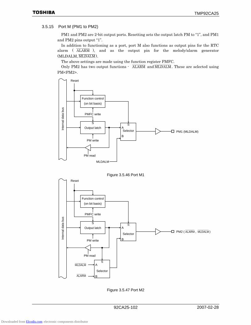
TMP92CA25
2007-02-28 92CA25-102
3.5.15 Port M (PM1 to PM2)
PM1 and PM2 are 2-bit output ports. Resetting sets the output latch PM to “1”, and PM1 and PM2 pins output “1”.
In addition to functioning as a port, port M also functions as output pins for the RTC alarm ( ALARM ), and as the output pin for the melody/alarm generator (MLDALM, MLDALM ).
The above settings are made using the function register PMFC. Only PM2 has two output functions - ALARM and MLDALM . These are selected using
PM<PM2>.
Figure 3.5.46 Port M1
Figure 3.5.47 Port M2
Inte
rnal
dat
a bu
s
Reset
S Output latch
PM write
SA Selector
B
PM read
PM1 (MLDALM)
Function control (on bit basis)
PMFC write
MLDALM
Inte
rnal
dat
a bu
s
Reset
S Output latch
PM write
SA
Selector
B
PM read
PM2 ( ALARM , MLDALM )
Function control (on bit basis)
PMFC write
MLDALMS
A
Selector
B ALARM
Downloaded from Elcodis.com electronic components distributor

TMP92CA25
2007-02-28 92CA25-103
Port M Register 7 6 5 4 3 2 1 0
Bit symbol PM2 PM1 PM (0058H) Read/Write R/W After reset 1 1
Port M Function Register 7 6 5 4 3 2 1 0
Bit symbol PM2F PM1F PMFC (005BH) Read/Write W After reset 0 0 Function 0: Port
1: ALARM at <PM2> = “1”
1: MLDALM at <PM2> = “0”
0: Port
1: MLDALM output
Port M Drive Register 7 6 5 4 3 2 1 0
Bit symbol PM2D PM1D PMDR (0096H) Read/Write R/W
After reset 1 1 Function Input/Output buffer drive
register for standby mode
Note: Read-modify-write is prohibited for the register PMFC.
Figure 3.5.48 Register for Port M
Downloaded from Elcodis.com electronic components distributor

TMP92CA25
2007-02-28 92CA25-104
3.5.16 Port N (PN0 to PN7)
PN0 to PN7 are 8-bit general-purpose I/O port. Each bit can be set individually for input or output. Resetting sets Port N to an input port. In addition to functioning as a general-purpose I/O port, Port N can also as interface pin for key-board (KO0 to KO7). This function can set to open-drain type output buffer.
Figure 3.5.49 Port N
Inte
rnal
dat
a bu
s
Direction control (on bit basis)
Reset
PNCR write
PN write
PN read
PN0 to PN7 (KO0 to KO7)
Function control (on bit basis)
PNFC write
S Output latch
SB
SelectorA
Open drian enable
Downloaded from Elcodis.com electronic components distributor
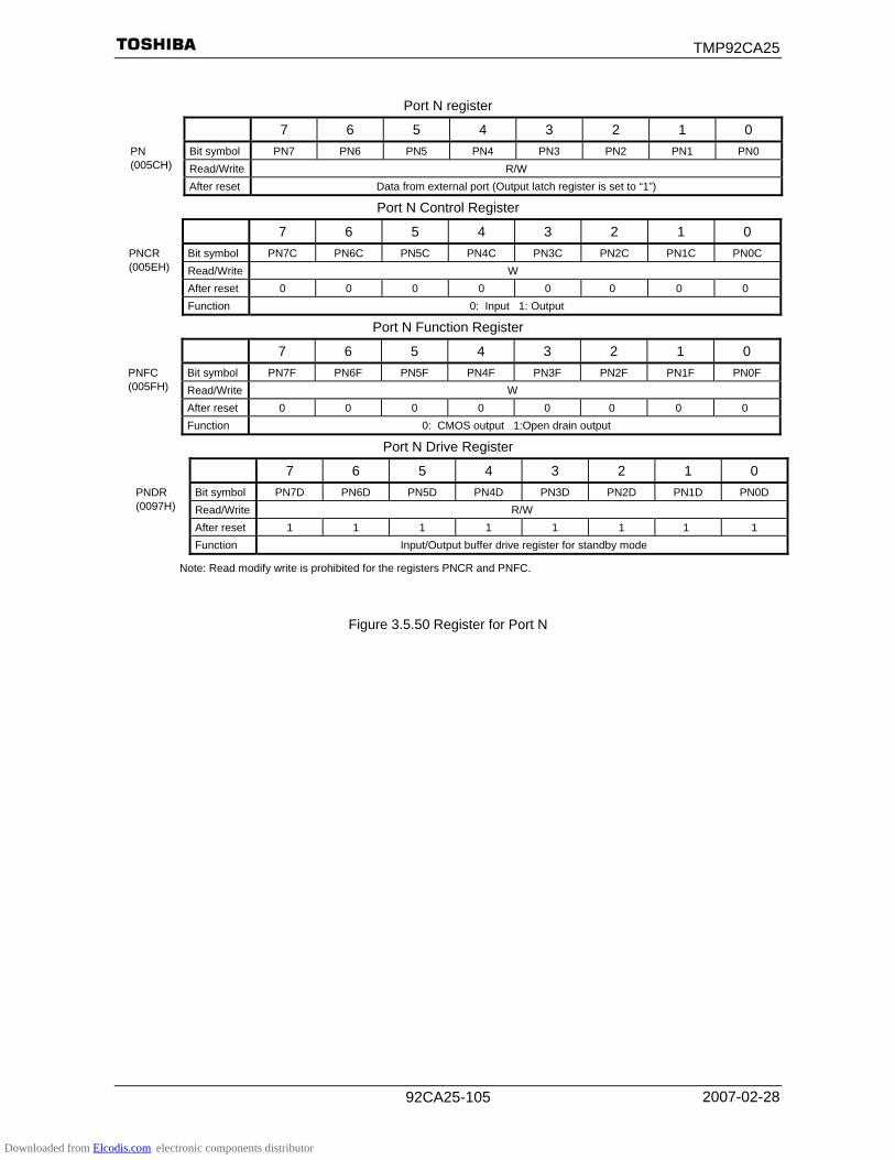
TMP92CA25
2007-02-28 92CA25-105
Port N register
7 6 5 4 3 2 1 0 Bit symbol PN7 PN6 PN5 PN4 PN3 PN2 PN1 PN0 PN
(005CH) Read/Write R/W After reset Data from external port (Output latch register is set to “1”)
Port N Control Register 7 6 5 4 3 2 1 0
Bit symbol PN7C PN6C PN5C PN4C PN3C PN2C PN1C PN0C PNCR (005EH) Read/Write W
After reset 0 0 0 0 0 0 0 0 Function 0: Input 1: Output
Port N Function Register 7 6 5 4 3 2 1 0
Bit symbol PN7F PN6F PN5F PN4F PN3F PN2F PN1F PN0F PNFC (005FH) Read/Write W
After reset 0 0 0 0 0 0 0 0 Function 0: CMOS output 1:Open drain output
Port N Drive Register 7 6 5 4 3 2 1 0
Bit symbol PN7D PN6D PN5D PN4D PN3D PN2D PN1D PN0D PNDR (0097H) Read/Write R/W
After reset 1 1 1 1 1 1 1 1 Function Input/Output buffer drive register for standby mode
Note: Read modify write is prohibited for the registers PNCR and PNFC.
Figure 3.5.50 Register for Port N
Downloaded from Elcodis.com electronic components distributor
TMP92CA25
2007-02-28 92CA25-106
3.6 Memory Controller
3.6.1 Functions
The TMP92CA25 has a memory controller with a variable 4-block address area that controls as follows. (1) 4-block address area support
Specifies a start address and a block size for the 4-block address area (block 0 to 3). • SRAM or ROM: All CS blocks (CS0 to CS3) are supported. • SDRAM : Only either CS1 or CS2 blocks are supported. • Page ROM : Only CS2 blocks are supported. • NAND flash : CS setting is not needed.
(2) Connecting memory specifications Specifies SRAM, ROM and SDRAM as memories that connect with the selected
address areas.
(3) Data bus width selection Whether 8 bits, 16 bits is selected as the data bus width of the respective block
address areas.
(4) Wait control Wait specification bit in the control register and WAIT input pin control the number
of waits in the external bus cycle. Read cycle and write cycle can specify the number of waits individually.
The number of waits is controlled in the 6 modes listed below. 0 waits, 1 wait, 2 waits, 3 waits, 4 waits N waits (controls with WAIT pin)
3.6.2 Control Register and Operation after Reset Release
This section describes the registers that control the memory controller, the state following reset release and the necessary settings. (1) Control register
The control registers of the memory controller are as follows and in Table 3.6.1 and Table 3.6.2. • Control register: BnCSH/BnCSL (n = 0 to 3, EX)
Sets the basic functions of the memory controller; the memory type that is connected, the number of waits which are read and written.
• Memory start address register: MSARn (n = 0 to 3) Sets a start address in the selected address areas.
• Memory address mask register: MAMR (n = 0 to 3) Sets a block size in the selected address areas.
• Page ROM control register: PMEMCR Sets the method of accessing page ROM.
• Memory controls control register: MEMCR0 Sets waveform selection of RD pin and setting method of 0CS to 3CS .
Downloaded from Elcodis.com electronic components distributor

TMP92CA25
2007-02-28 92CA25-107
Table 3.6.1 Control Register
7 6 5 4 3 2 1 0 Bit symbol B0WW2 B0WW1 B0WW0 B0WR2 B0WR1 B0WR0 B0CSL
(0140H) Read/Write W W After reset 0 1 0 0 1 0
Bit symbol B0E − − B0REC B0OM1 B0OM0 B0BUS1 B0BUS0B0CSH (0141H) Read/Write W After reset 0 0 (Note) 0 (Note) 0 0 0 0 0
Bit symbol M0V20 M0V19 M0V18 M0V17 M0V16 M0V15 M0V14 to M0V9
M0V8 MAMR0 (0142H)
Read/Write R/W After reset 1 1 1 1 1 1 1 1
Bit symbol M0S23 M0S22 M0S21 M0S20 M0S19 M0S18 M0S17 M0S16 MSAR0 (0143H) Read/Write R/W After reset 1 1 1 1 1 1 1 1
Bit symbol B1WW2 B1WW1 B1WW0 B1WR2 B1WR1 B1WR0 B1CSL (0144H) Read/Write W W After reset 0 1 0 0 1 0
Bit symbol B1E − − B1REC B1OM1 B1OM0 B1BUS1 B1BUS0B1CSH (0145H) Read/Write W After reset 0 0 (Note) 0 (Note) 0 0 0 0 0
Bit symbol M1V21 M1V20 M1V19 M1V18 M1V17 M1V16 M1V15 to M1V9
M1V8 MAMR1 (0146H)
Read/Write R/W After reset 1 1 1 1 1 1 1 1
Bit symbol M1S23 M1S22 M1S21 M1S20 M1S19 M1S18 M1S17 M1S16 MSAR1 (0147H) Read/Write R/W After reset 1 1 1 1 1 1 1 1
Bit symbol B2WW2 B2WW1 B2WW0 B2WR2 B2WR1 B2WR0 B2CSL (0148H) Read/Write W W After reset 0 1 0 0 1 0
Bit symbol B2E B2M − B2REC B2OM1 B2OM0 B2BUS1 B2BUS0B2CSH (0149H) Read/Write W After reset 1 0 0 (Note) 0 0 0 0 0
Bit symbol M2V22 M2V21 M2V20 M2V19 M2V18 M2V17 M2V16 M2V15 MAMR2 (014AH) Read/Write R/W After reset 1 1 1 1 1 1 1 1
Bit symbol M2S23 M2S22 M2S21 M2S20 M2S19 M2S18 M2S17 M2S16 MSAR2 (014BH) Read/Write R/W After reset 1 1 1 1 1 1 1 1
Bit symbol B3WW2 B3WW1 B3WW0 B3WR2 B3WR1 B3WR0 B3CSL (014CH) Read/Write W W After reset 0 1 0 0 1 0
Bit symbol B3E − − B3REC B3OM1 B3OM0 B3BUS1 B3BUS0B3CSH (014DH) Read/Write W After reset 0 0 (Note) 0 (Note) 0 0 0 0 0
Bit symbol M3V22 M3V21 M3V20 M3V19 M3V18 M3V17 M3V16 M3V15 MAMR3 (014EH) Read/Write R/W After reset 1 1 1 1 1 1 1 1
Bit symbol M3S23 M3S22 M3S21 M3S20 M3S19 M3S18 M3S17 M3S16 MSAR3 (014FH) Read/Write R/W After reset 1 1 1 1 1 1 1 1
Note 1: Always write “0”.
Note 2:Read-modify-write is prohibited for BnCS0 and BnCSH (n = 0 to 3) registers.
Downloaded from Elcodis.com electronic components distributor
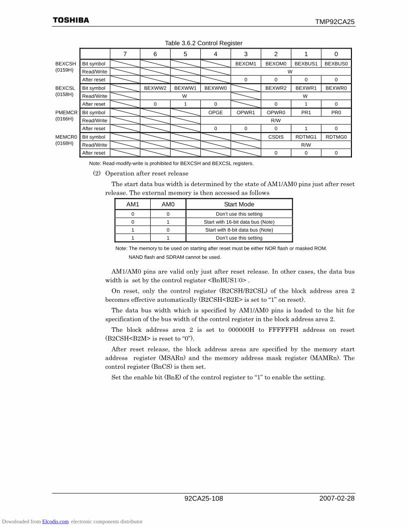
TMP92CA25
2007-02-28 92CA25-108
Table 3.6.2 Control Register 7 6 5 4 3 2 1 0
Bit symbol BEXOM1 BEXOM0 BEXBUS1 BEXBUS0BEXCSH (0159H) Read/Write W After reset 0 0 0 0
Bit symbol BEXWW2 BEXWW1 BEXWW0 BEXWR2 BEXWR1 BEXWR0BEXCSL (0158H) Read/Write W W After reset 0 1 0 0 1 0
Bit symbol OPGE OPWR1 OPWR0 PR1 PR0 PMEMCR (0166H) Read/Write R/W After reset 0 0 0 1 0
Bit symbol CSDIS RDTMG1 RDTMG0MEMCR0 (0168H) Read/Write R/W After reset 0 0 0
Note: Read-modify-write is prohibited for BEXCSH and BEXCSL registers.
(2) Operation after reset release The start data bus width is determined by the state of AM1/AM0 pins just after reset
release. The external memory is then accessed as follows
AM1 AM0 Start Mode 0 0 Don’t use this setting 0 1 Start with 16-bit data bus (Note) 1 0 Start with 8-bit data bus (Note) 1 1 Don’t use this setting
Note: The memory to be used on starting after reset must be either NOR flash or masked ROM.
NAND flash and SDRAM cannot be used.
AM1/AM0 pins are valid only just after reset release. In other cases, the data bus width is set by the control register <BnBUS1:0> .
On reset, only the control register (B2CSH/B2CSL) of the block address area 2 becomes effective automatically (B2CSH<B2E> is set to “1” on reset).
The data bus width which is specified by AM1/AM0 pins is loaded to the bit for specification of the bus width of the control register in the block address area 2.
The block address area 2 is set to 000000H to FFFFFFH address on reset (B2CSH<B2M> is reset to “0”).
After reset release, the block address areas are specified by the memory start address register (MSARn) and the memory address mask register (MAMRn). The control register (BnCS) is then set.
Set the enable bit (BnE) of the control register to “1” to enable the setting.
Downloaded from Elcodis.com electronic components distributor

TMP92CA25
2007-02-28 92CA25-109
3.6.3 Basic Functions and Register Setting
This section describes the setting of the block address area, the connecting memory and the number of waits out of the memory controller’s functions. (1) Block address area specification
The block address area is specified by two registers. The memory start address register (MSARn) sets the start address of the block
address areas. The memory controller compares the register value and the address every bus cycle. The address bit which is masked by the memory address mask register (MAMRn) is not compared by the memory controller. The block address area size is determined by setting the memory address mask register. The value that is set to the register is compared with the block address area on the bus. If the result is a match, the memory controller sets the chip select signal (CSn) to “low”.
(i) Memory start address register setting
The MS23 to MS16 bits of the memory start address register correspond with addresses A23 to A16 respectively. The lower start addresses A15 to A0 are always set to address 0000H.
Therefore the start addresses of the block address area are set to all 64 Kbytes of addresses 000000H to FF0000H.
(ii) Memory address mask register setting
The memory address mask register determines whether an address bit is compared or not. In register setting, “0” is “compare”, and “1” is “do not compare”.
The address bits that can be set depends on the block address area. Block address area 0: A20 to A8 Block address area 1: A21 to A8 Block address area 2 to 3: A22 to A15
The upper bits are always compared. The block address area size is determined by the result of the comparison.
The size to be set depending on the block address area is as follows.
Size (bytes)
CS area 256 512 32 K 64 K 128 K 256 K 512 K 1 M 2 M 4 M 8 M
CS0 ○ ○ ○ ○ ○ ○ ○ ○ ○ CS1 ○ ○ ○ ○ ○ ○ ○ ○ ○
CS2 to CS3 ○ ○ ○ ○ ○ ○ ○ ○ ○
Note: After reset release, only the control register of the block address area 2 is valid. The control register of block address area 2 has the <B2M> bit. If the <B2M> bit is set to “0”, block address area 2 is set to addresses 000000H to FFFFFFH. (This is the state following reset release .) If the <B2M> bit is set to “1”, the start address and the address area size are set, as in the other block address areas.
Downloaded from Elcodis.com electronic components distributor
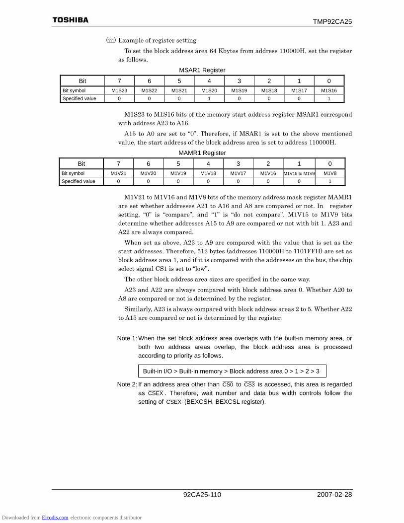
TMP92CA25
2007-02-28 92CA25-110
(iii) Example of register setting To set the block address area 64 Kbytes from address 110000H, set the register
as follows. MSAR1 Register
Bit 7 6 5 4 3 2 1 0 Bit symbol M1S23 M1S22 M1S21 M1S20 M1S19 M1S18 M1S17 M1S16 Specified value 0 0 0 1 0 0 0 1
M1S23 to M1S16 bits of the memory start address register MSAR1 correspond
with address A23 to A16. A15 to A0 are set to “0”. Therefore, if MSAR1 is set to the above mentioned
value, the start address of the block address area is set to address 110000H. MAMR1 Register
Bit 7 6 5 4 3 2 1 0 Bit symbol M1V21 M1V20 M1V19 M1V18 M1V17 M1V16 M1V15 to M1V9 M1V8 Specified value 0 0 0 0 0 0 0 1
M1V21 to M1V16 and M1V8 bits of the memory address mask register MAMR1
are set whether addresses A21 to A16 and A8 are compared or not. In register setting, “0” is “compare”, and “1” is “do not compare”. M1V15 to M1V9 bits determine whether addresses A15 to A9 are compared or not with bit 1. A23 and A22 are always compared.
When set as above, A23 to A9 are compared with the value that is set as the start addresses. Therefore, 512 bytes (addresses 110000H to 1101FFH) are set as block address area 1, and if it is compared with the addresses on the bus, the chip select signal CS1 is set to “low”.
The other block address area sizes are specified in the same way. A23 and A22 are always compared with block address area 0. Whether A20 to
A8 are compared or not is determined by the register. Similarly, A23 is always compared with block address areas 2 to 5. Whether A22
to A15 are compared or not is determined by the register.
Note 1: When the set block address area overlaps with the built-in memory area, or both two address areas overlap, the block address area is processed according to priority as follows.
Note 2: If an address area other than 0CS to 3CS is accessed, this area is regarded as CSEX . Therefore, wait number and data bus width controls follow the setting of CSEX (BEXCSH, BEXCSL register).
Built-in I/O > Built-in memory > Block address area 0 > 1 > 2 > 3
Downloaded from Elcodis.com electronic components distributor

TMP92CA25
2007-02-28 92CA25-111
(2) Connection memory specification Setting the <BnOM1:0> bit of the control register (BnCSH) specifies the memory
type that is connected with the block address areas. The interface signal is outputted according to the set memory as follows.
<BnOM1: 0> Bit (BnCSH Register)
<BnOM1> <BnOM0> Function 0 0 SRAM/ROM (Default) 0 1 Reserved 1 0 Reserved 1 1 SDRAM
Note 1: SDRAM should be set to block either 1 or 2.
Note 2: Set “00” for NAND flash, RAM built-in LCDD.
(3) Data bus width specification The data bus width is set for every block address area. The bus size is set by setting
the control register (BnCSH)<BnBUS1:0> as follows.
<BnBUS1:0> bit (BnCSH Register)
BnBUS 1 BnBUS 0 Function 0 0 8-bit bus mode (Default) 0 1 16-bit bus mode 1 0 Reserved 1 1 Don’t use this setting
Note: SDRAM should be set to either “01” (16-bit bus).
This method of changing the data bus width depending on the accessing address is called “dynamic bus sizing”. The part of the data bus to which the data is output depends on the data size, baus width and start address.
Number of external data bus pin in TMP92CA25 are 16 pins. Therefore, please ignore case of memory data size is 32 in each tables.
Note: Since there is a possibility of abnormal writing/reading of the data if two memories with different bus width are put in consecutive addresses, do not execute an access to both memories with one command.
Downloaded from Elcodis.com electronic components distributor

TMP92CA25
2007-02-28 92CA25-112
CPU Data Operand Data
Size (bit)
Operand Start
Address
Memory Data Size
(bit) CPU Address
D31 to D24 D23 to D16 D15 to D8 D7 to D0
4n + 0 8/16/32 4n + 0 xxxxx xxxxx xxxxx b7 to b08 4n + 1 xxxxx xxxxx xxxxx b7 to b04n + 1
16/32 4n + 1 xxxxx xxxxx b7 to b0 xxxxx 8/16 4n + 2 xxxxx xxxxx xxxxx b7 to b04n + 2 32 4n + 2 xxxxx b7 to b0 xxxxx xxxxx 8 4n + 3 xxxxx xxxxx xxxxx b7 to b0
16 4n + 3 xxxxx xxxxx b7 to b0 xxxxx
8
4n + 3
32 4n + 3 b7 to b0 xxxxx xxxxx xxxxx (1) 4n + 0 xxxxx xxxxx xxxxx b7 to b08 (2) 4n + 1 xxxxx xxxxx xxxxx b15 to b8
4n + 0
16/32 4n + 0 xxxxx xxxxx b15 to b8 b7 to b0(1) 4n + 1 xxxxx xxxxx xxxxx b7 to b08 (2) 4n + 2 xxxxx xxxxx xxxxx b15 to b8(1) 4n + 1 xxxxx xxxxx b7 to b0 xxxxx 16 (2) 4n + 2 xxxxx xxxxx xxxxx b15 to b8
4n + 1
32 4n + 1 xxxxx b15 to b8 b7 to b0 xxxxx (1) 4n + 2 xxxxx xxxxx xxxxx b7 to b08 (2) 4n + 1 xxxxx xxxxx xxxxx b15 to b8
16 4n + 2 xxxxx xxxxx b15 to b8 b7 to b0
4n + 2
32 4n + 2 b15 to b8 b7 to b0 xxxxx xxxxx (1) 4n + 3 xxxxx xxxxx xxxxx b7 to b08 (2) 4n + 4 xxxxx xxxxx xxxxx b15 to b8(1) 4n + 3 xxxxx xxxxx b7 to b0 xxxxx 16 (2) 4n + 4 xxxxx xxxxx xxxxx b15 to b8(1) 4n + 3 b7 to b0 xxxxx xxxxx xxxxx
16
4n + 3
32 (2) 4n + 4 xxxxx xxxxx xxxxx b15 to b8(1) 4n + 0 xxxxx xxxxx xxxxx b7 to b0(2) 4n + 1 xxxxx xxxxx xxxxx b15 to b8(3) 4n + 2 xxxxx xxxxx xxxxx b23 to b16
8
(4) 4n + 3 xxxxx xxxxx xxxxx b31 to b24(1) 4n + 0 xxxxx xxxxx b15 to b8 b7 to b016 (2) 4n + 2 xxxxx xxxxx b31 to b24 b23 to b16
4n + 0
32 4n + 0 b31 to b24 b23 to b16 b15 to b8 b7 to b0(1) 4n + 0 xxxxx xxxxx xxxxx b7 to b0(2) 4n + 1 xxxxx xxxxx xxxxx b15 to b8(3) 4n + 2 xxxxx xxxxx xxxxx b23 to b16
8
(4) 4n + 3 xxxxx xxxxx xxxxx b31 to b24(1) 4n + 1 xxxxx xxxxx b7 to b0 xxxxx (2) 4n + 2 xxxxx xxxxx b23 to b16 b15 to b8
16
(3) 4n + 4 xxxxx xxxxx xxxxx b31 to b24(1) 4n + 1 b23 to b16 b15 to b8 b7 to b0 xxxxx
4n + 1
32 (2) 4n + 4 xxxxx xxxxx xxxxx b31 to b24(1) 4n + 2 xxxxx xxxxx xxxxx b7 to b0(2) 4n + 3 xxxxx xxxxx xxxxx b15 to b8(3) 4n + 4 xxxxx xxxxx xxxxx b23 to b16
8
(4) 4n + 5 xxxxx xxxxx xxxxx b31 to b24(1) 4n + 2 xxxxx xxxxx b15 to b8 b7 to b016 (2) 4n + 4 xxxxx xxxxx b31 to b24 b23 to b16(1) 4n + 2 b15 to b8 b7 to b0 xxxxx xxxxx
4n + 2
32 (2) 4n + 4 xxxxx xxxxx b31 to b24 b23 to b16(1) 4n + 3 xxxxx xxxxx xxxxx b7 to b0(2) 4n + 4 xxxxx xxxxx xxxxx b15 to b8(3) 4n + 5 xxxxx xxxxx xxxxx b23 to b16
8
(4) 4n + 6 xxxxx xxxxx xxxxx b31 to b24(1) 4n + 3 xxxxx xxxxx b7 to b0 xxxxx (2) 4n + 4 xxxxx xxxxx b23 to b16 b15 to b8
16
(3) 4n + 6 xxxxx xxxxx xxxxx b31 to b24(1) 4n + 3 b7 to b0 xxxxx xxxxx xxxxx
32
4n + 3
32 (2) 4n + 4 xxxxx b31 to b24 b23 to b16 b15 to b8
xxxxx: During a read, data input to the bus ignored. At write, the bus is at high impedance and the write strobe signal remains non active.
Downloaded from Elcodis.com electronic components distributor
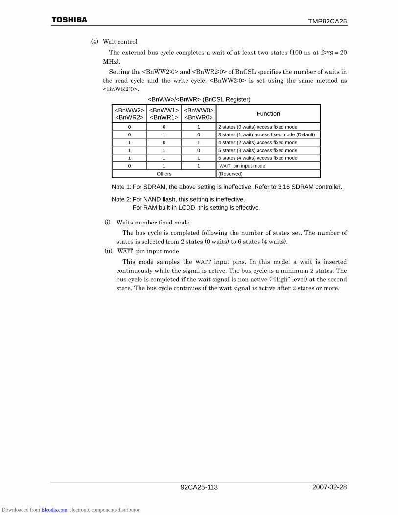
TMP92CA25
2007-02-28 92CA25-113
(4) Wait control The external bus cycle completes a wait of at least two states (100 ns at fSYS = 20
MHz). Setting the <BnWW2:0> and <BnWR2:0> of BnCSL specifies the number of waits in
the read cycle and the write cycle. <BnWW2:0> is set using the same method as <BnWR2:0>.
<BnWW>/<BnWR> (BnCSL Register)
<BnWW2> <BnWR2>
<BnWW1><BnWR1>
<BnWW0><BnWR0> Function
0 0 1 2 states (0 waits) access fixed mode 0 1 0 3 states (1 wait) access fixed mode (Default) 1 0 1 4 states (2 waits) access fixed mode 1 1 0 5 states (3 waits) access fixed mode 1 1 1 6 states (4 waits) access fixed mode 0 1 1 WAIT pin input mode
Others (Reserved)
Note 1: For SDRAM, the above setting is ineffective. Refer to 3.16 SDRAM controller.
Note 2: For NAND flash, this setting is ineffective. For RAM built-in LCDD, this setting is effective.
(i) Waits number fixed mode
The bus cycle is completed following the number of states set. The number of states is selected from 2 states (0 waits) to 6 states (4 waits).
(ii) WAIT pin input mode This mode samples the WAIT input pins. In this mode, a wait is inserted
continuously while the signal is active. The bus cycle is a minimum 2 states. The bus cycle is completed if the wait signal is non active (“High” level) at the second state. The bus cycle continues if the wait signal is active after 2 states or more.
Downloaded from Elcodis.com electronic components distributor
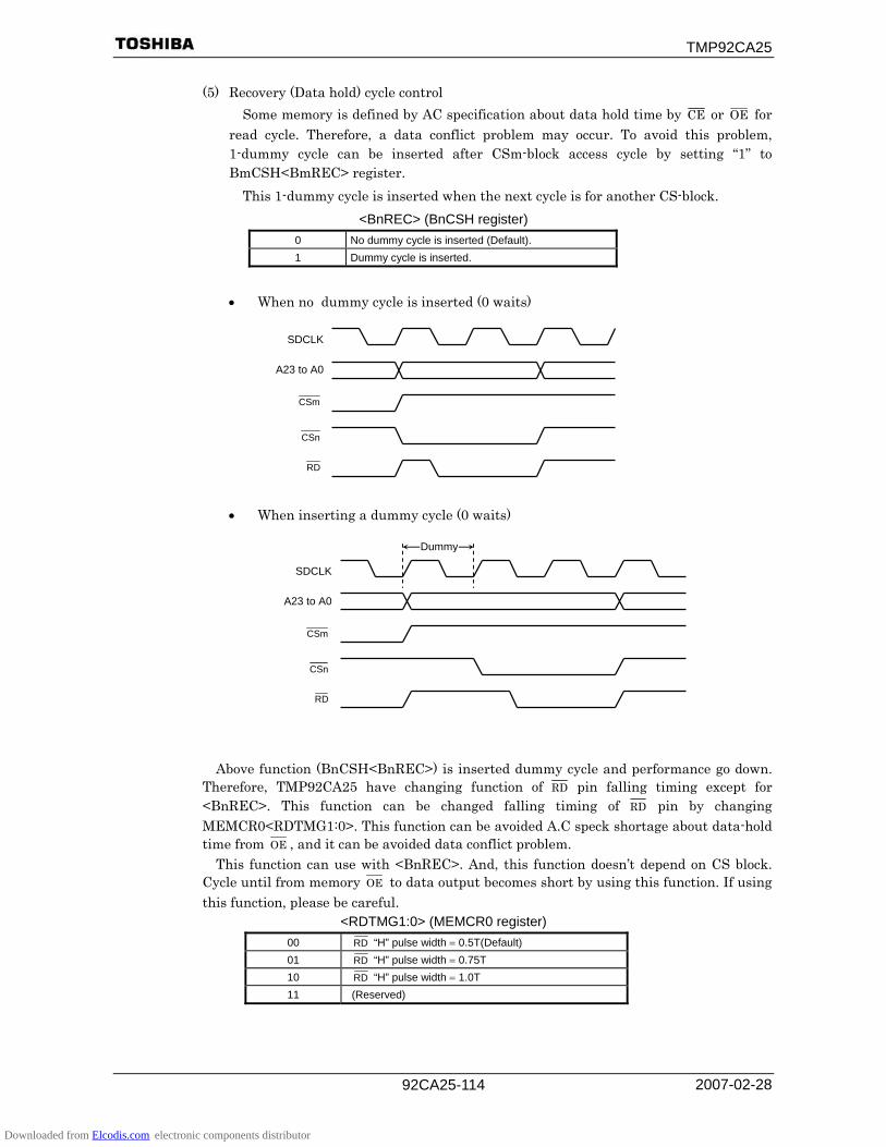
TMP92CA25
2007-02-28 92CA25-114
(5) Recovery (Data hold) cycle control Some memory is defined by AC specification about data hold time by CE or OE for
read cycle. Therefore, a data conflict problem may occur. To avoid this problem, 1-dummy cycle can be inserted after CSm-block access cycle by setting “1” to BmCSH<BmREC> register.
This 1-dummy cycle is inserted when the next cycle is for another CS-block. <BnREC> (BnCSH register)
0 No dummy cycle is inserted (Default). 1 Dummy cycle is inserted.
• When no dummy cycle is inserted (0 waits)
• When inserting a dummy cycle (0 waits)
Above function (BnCSH<BnREC>) is inserted dummy cycle and performance go down.
Therefore, TMP92CA25 have changing function of RD pin falling timing except for <BnREC>. This function can be changed falling timing of RD pin by changing MEMCR0<RDTMG1:0>. This function can be avoided A.C speck shortage about data-hold time from OE , and it can be avoided data conflict problem.
This function can use with <BnREC>. And, this function doesn’t depend on CS block. Cycle until from memory OE to data output becomes short by using this function. If using this function, please be careful.
<RDTMG1:0> (MEMCR0 register) 00 RD “H” pulse width = 0.5T(Default) 01 RD “H” pulse width = 0.75T 10 RD “H” pulse width = 1.0T 11 (Reserved)
SDCLK
A23 to A0
CSm
CSn
RD
SDCLK
A23 to A0
CSm
CSn
RD
Dummy
Downloaded from Elcodis.com electronic components distributor

TMP92CA25
2007-02-28 92CA25-115
A23 to A0
CSn
T1 T2
SDCLK (20MHz)
SRxxB
InputD15 to D0
<RDTMGD1:0>= “00”
<RDTMGD1:0>= “01”
<RDTMGD1:0>= “10”
RD
Downloaded from Elcodis.com electronic components distributor

TMP92CA25
2007-02-28 92CA25-116
(6) Basic bus timing (a) External read/write cycle (0 waits)
(b) External read/write cycle (1 wait)
CSn
WRxx
RD , SRxxB
A23 to A0
Input
Output
Read
Write
SDCLK (20 MHz)
D15 to D0
D15 to D0
T1 T2
SRWR , SRxxB
CSn
WRxx
RD , SRxxB
A23 to A0
Output
SDCLK (20 MHz)
D15 to D0
D15 to D0
T1 TW
InputRead
Write
T2
SRWR , SRxxB
Downloaded from Elcodis.com electronic components distributor

TMP92CA25
2007-02-28 92CA25-117
(c) External read/write cycle (0 waits at WAIT pin input mode)
(d) External read/write cycle (n waits at WAIT pin input mode)
CSn
WRxx
RD , SRxxB
A23 to A0
Input
Output
Read
Write
SDCLK (20 MHz)
D15 to D0
D15 to D0
T1 T2
SRWR , SRxxB
WAIT
Sampling
CSn
WRxx
RD , SRxxB
A23 to A0
Output
SDCLK (20 MHz)
D15 to D0
D15 to D0
T1 TW
Input Read
Write
T2
SRWR , SRxxB
WAIT
Sampling Sampling
Downloaded from Elcodis.com electronic components distributor

TMP92CA25
2007-02-28 92CA25-118
Example of wait input cycle (5 waits)
CSn
SRWR RD
WAITD Q CK
RES
D Q CK
RES
D Q CK
RES
D Q CK
RES
D Q CK
RES
SDCLK
FF0 FF1 FF2 FF3 FF4
SDCLK (20 MHz)
1 2 3 4 5 6 7
CSn
RD
WAIT
FF_RES
FF0_D
FF0_Q
FF1_Q
FF2_Q
FF3_Q
Downloaded from Elcodis.com electronic components distributor
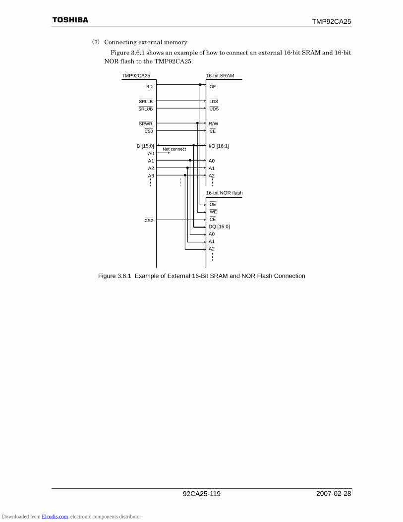
TMP92CA25
2007-02-28 92CA25-119
(7) Connecting external memory Figure 3.6.1 shows an example of how to connect an external 16-bit SRAM and 16-bit
NOR flash to the TMP92CA25.
Figure 3.6.1 Example of External 16-Bit SRAM and NOR Flash Connection
TMP92CA25 16-bit SRAM
RD
SRLLB
SRLUB
SRWR
0CS
D [15:0]A0A1A2A3
2CS
OE LDS UDS R/W CE I/O [16:1] A0 A1 A2
16-bit NOR flash
OE WE CE DQ [15:0] A0 A1 A2
Not connect
Downloaded from Elcodis.com electronic components distributor

TMP92CA25
2007-02-28 92CA25-120
3.6.4 ROM Control (Page mode)
This section describes ROM page mode accessing and how to set registers. ROM page mode is set by the page ROM control register. (1) Operation and how to set the registers
The TMP92CA25 supports ROM access of the page mode. ROM access of the page mode is specified only in block address area 2.
ROM page mode is set by the page ROM control register (PMEMCR). Setting <OPGE> of the PMEMCR register to “1” sets the memory access of the block address area to ROM page mode access.
The number of read cycles is set by the <OPWR1:0> of the PMEMCR register.
<OPWR1:0> (PMEMCR register)
<OPWR1> <OPWR0> Number of Cycle in a Page 0 0 1 state (n-1-1-1 mode) (n ≥ 2) 0 1 2 state (n-2-2-2 mode) (n ≥ 3) 1 0 3 state (n-3-3-3 mode) (n ≥ 4) 1 1 (Reserved)
Note: Set the number of waits (“n”) using the control register (BnCSL) in each block address area.
The page size (the number of bytes) of ROM in the CPU size is set by the <PR1:0> of the PMEMCR register. When data is read out up to the border of the set page, the controller completes the page reading operation. The start data of the next page is read in the normal cycle. The following data is set to page read again.
<PR1:0> Bit (PMEMCR register)
<PR1> <PR0> ROM Page Size 0 0 64 bytes 0 1 32 bytes 1 0 16 bytes (Default) 1 1 8 bytes
Figure 3.6.2 Page mode access Timing (8-byte example)
SDCLK
A0 to A23
2CS
RD
D0 to D31
+0 +1 +2 +3
Datainput
Datainput
Data input
Data input
tAD3 tAD2 tAD2 tAD2 tHA
tHRtRD3 tHA tHAtHA
tCYC
Downloaded from Elcodis.com electronic components distributor

TMP92CA25
2007-02-28 92CA25-121
3.6.5 Cautions
(1) Note on timing between CS and RD If the parasitic capacitance of the RD (Read signal) is greater than that of the CS
(Chip select signal), it is possible that an unintended read cycle occurs due to a delay in the read signal. Such an unintended read cycle may cause a problem, as in the case of (a) in Figure 3.6.3.
Figure 3.6.3 Read Signal Delay Read Cycle
Example: When using an externally connected NOR flash which uses JEDEC standard commands, note that the toggle bit may not be read out correctly. If the read signal in the cycle immediately preceding the access to the NOR flash does not go high in time, as shown in Figure 3.6.4, an unintended read cycle like the one shown in (b) may occur.
Figure 3.6.4 NOR Flash Toggle Bit Read Cycle
When the toggle bit is reversed by this unexpected read cycle, the CPU cannot read the toggle bit correctly since it always reads same value for the toggle bit. To avoid this phenomenon, data polling function control is recommended.
RD
A23 to A0
SDCLK (20 MHz)
CSm
CSn
(a)
A23 to A0
SDCLK(20 MHz)
NOR flashchip select
RD
(b)
Toggle bit
Memory access Toggle bit RD cycle
Downloaded from Elcodis.com electronic components distributor

TMP92CA25
2007-02-28 92CA25-122
(2) Note on NAND flash area setting, LCD driver area setting with built-in RAM Figure 3.6.5 shows a memory map for a NAND flash and RAM built-in LCD driver. Since it is recommended that CS3 area be assigned to the address 000000H to
3FFFFFH, the following explanation is given. In this case, the NAND flash and RAM built-in LCD driver overlap with CS3 area. However, each access control circuit in the TMP92CA25 operates independently. So, if a program on CS3 area accesses NAND flash, both CS3 and NAND flash will
be accessed at the same time and a problem such as data conflict will occur. To avoid this phenomenon, TMP92CA25 have MEMCR0<CSDIS>. If set <CSDIS> to
“1”, CS3 pin don’t active in case of access 001D00H to 001FFFH (768B) in area that is set as CS3 area. Above phenomenon can be avoided by this setting. This function is valid not only CS3 but also all 0CS to 3CS pins.
Note1: In above setting, the address from 000000H to 005FFFH of 24 Kbytes for CS3’s memory can’t be used.
Note2: 512 byte area (001D00H to 001EFFH) for NAND flash are fixedlike a following without relation ship to setting CS block. Therefore, NAND flash area don’t conform to CS3 area setting. (NAND flash area specification) 1. bus width : Fixed 8 bit 2. WAIT control : Depend on NDnFSPR<SPW> of NAND flash controller
Figure 3.6.5 Recommended CS3 and CS0 Setting
NAND flash (512byte)
(No assigned)
LCDD with built-in RAM (16byte)
COMMON-X (2 M byte)
LOCAL-X (2 M byte)
Internal I/O
Internal RAM (10K byte)
0CS ∼ 3CS pins become to Non-active by setting MEMCR0<CSDIS> to “1”
000000H
001D00H
001F00H
001FE0H001FF0H002000H
400000H
004800H
008000H
200000HCS3 area setting 000000H~3FFFFFH (4 MB)
Downloaded from Elcodis.com electronic components distributor

TMP92CA25
2007-02-28 92CA25-123
(3) The cautions at the time of the functional change of a CSn . A chip select signal output has the case of a combination terminal with a general-purpose
port function. In this case, an output latch register and a function control register are initialized by the reset action, and an object terminal is initialized by the port output (“1” or “0”) by it.
Functional change Although an object terminal is changed from a port to a chip select signal output by
setting up a function control register (PnFC register), the short pulse for several ns may be outputted to the changing timing. Although it does not become especially a problem when using the usual memory, it may become a problem when using a special memory.
XX n+2 Internal address bus
Function control signal
Pxx n n+2 A23 to A0
A port is set as CSn .
n
Output port CSn
Inte
rnal
Si
gnal
Ex
tern
al
Sign
al
Output pulse tAD3
* XX is a function register address.(When an output port is initialized by “0”)
The measure by software The countermeasures in S/W for avoiding this phenomenon are explained. Since CS signal decodes the address of the access area and is generated, an
unnecessary pulse is outputted by access to the object CS area immediately after setting it as a CSn function. Then, if internal area is accessed also immediately after setting a port as CS function, an unnecessary pulse will not output.
1. The ban on interruption under functional change (DI command) 2. A dummy command is added in order to carry out continuous internal access. 3. (Access to a functional change register is corresponded by 16-bit command.
(LDW command))
XX+1 n+2 Internal address bus
Function control signal
Pxx
n n+2 A23 to A0
A port is set as CSn .
XX
Output port CSn
Inte
rnal
si
gnal
E
xter
nal
sign
al
Dummy access
Downloaded from Elcodis.com electronic components distributor

TMP92CA25
2007-02-28 92CA25-124
3.7 8-Bit Timers (TMRA)
The TMP92CA25 features 4 built-in 8-bit timers (TMRA0-TMRA3). These timers are paired into two modules: TMRA01 and TMRA23. Each module consists of two channels and can operate in any of the following four operating modes.
• 8-bit interval timer mode
• 16-bit interval timer mode • 8-bit programmable square wave pulse generation output mode
(PPG: Variable duty cycle with variable period)
• 8-bit pulse width modulation output mode (PWM: Variable duty cycle with constant period)
Figure 3.7.1 and Figure 3.7.2 show block diagrams for TMRA01 and TMRA23. Each channel consists of an 8-bit up counter, an 8-bit comparator and an 8-bit timer register.
In addition, a timer flip-flop and a prescaler are provided for each pair of channels. The operation mode and timer flip-flops are controlled by a five-byte SFR (special function
register). Each of the two modules (TMRA01 and TMRA23) can be operated independently. All modules
operate in the same manner; hence only the operation of TMRA01 is explained here. The contents of this chapter are as follows.
3.7.1 Block Diagrams 3.7.2 Operation of Each Circuit 3.7.3 SFR 3.7.4 Operation in Each Mode
(1) 8-bit timer mode (2) 16-bit timer mode (3) 8-bit PPG (programmable pulse generation) output mode (4) 8-bit PWM (pulse width modulation) output mode (5) Mode settings
Table 3.7.1 Registers and Pins for Each Module
Module
TMRA01 TMRA23
Input pin for external clock No No External
pin Output pin for timer flip-flop TA1OUT (Shared with PC0)
TA3OUT (Shared with PC1)
Timer run register TA01RUN (1100H) TA23RUN (1108H)
Timer register TA0REG (1102H) TA1REG (1103H)
TA2REG (110AH) TA3REG (110BH)
Timer mode register TA01MOD (1104H) TA23MOD (110CH)
SFR (Address)
Timer flip-flop control register TA1FFCR (1105H) TA3FFCR (110DH)
Downloaded from Elcodis.com electronic components distributor

TMP92CA25
2007-02-28 92CA25-125
3.7.1 Block Diagrams
Figure 3.7.1 TMRA01 Block Diagram
φT1
φT16
φT25
6
8-bi
t com
para
tor
(CP
1)
8-bi
t up
coun
ter
(CP
0)
8-bi
t up
coun
ter
(UC
0)
2n O
ver
flow
8-bi
t up
coun
ter
(UC
1)
Tim
er
flip-
flop
TA1F
F
Mat
ch
dete
ct
Mat
ch d
etec
t
8-bi
t tim
er
regi
ster
TA
1RE
G
φT1
φT4
φT16
512
256
128
64
32
16
8 4
2 φT1
φT4
φT16
φT
256
Run
/cle
ar
Pre
scal
er
TA01
MO
D
<TA
0CLK
1:0>
Pre
scal
e rcl
ock:
φT0
TA01
RU
N<T
A0R
UN
> S
elec
tor
8-bi
t tim
er re
gist
er
TA0R
EG
TA01
MO
D
<PW
M01
:00>
TA01
MO
D
<TA
01M
1:0>
TMR
A0
Inte
rrup
t out
put:
INTT
A0
TMR
A0
Inte
rrup
t out
put:
TA0T
RG
TA01
MO
D
<TA
1CLK
1:0>
TA01
RU
N<T
A1R
UN
>
TA1F
FCR
Tim
er fl
ip-fl
op
outp
ut: T
A1O
UT
TMR
A1
Inte
rrup
t out
put:
INTT
A1
Inte
rnal
data
bus
TA01
RU
N
<TA
0RD
E>
TA01
RU
N
<TA
01P
RU
N>
Sel
ecto
r
Inte
rnal
dat
a bu
s
TA0T
RG
Reg
iste
r bu
ffer 0
Downloaded from Elcodis.com electronic components distributor

TMP92CA25
2007-02-28 92CA25-126
Figure 3.7.2 TMRA23 Block Diagram
φT1
φT16
φT25
6
8-bi
t com
para
tor
(CP
3)
8-bi
t com
para
tor
(CP
2)
8-bi
t up
coun
ter
(UC
2)
2n O
ver
flow
8-bi
t up
com
para
tor
(UC
3)
Tim
er
flip-
flop
TA3F
F
Mat
chde
tect
M
atch
det
ect
8-bi
t tim
er
regi
ster
TA
3RE
G
φT1
φT4
φT16
512
256
128
64
32
16
8 4
2 φT1
φT4
φT16
φT
256
Run
/cle
ar
Pre
scal
er
TA23
MO
D
<TA
2CLK
1:0>
Pre
scal
e rcl
ock:
φT0
TA23
RU
N<T
A2R
UN
> S
elec
tor
8-bi
t tim
er re
gist
er
TA2R
EG
TA23
MO
D
<PW
M21
:20>
TA23
MO
D
<TA
23M
1:0>
TMR
A2
Inte
rrup
t out
put:
INTT
A2
TMR
A2
Inte
rrup
t out
put:
TA
2TR
G
TA23
MO
D
<TA
3CLK
1:0>
TA23
RU
N<T
A3R
UN
>
TA3F
FCR
Tim
er fl
ip-fl
op
outp
ut: T
A3O
UT
TMR
A3
Inte
rrup
t out
put:
INTT
A3
Inte
rnal
dat
a bu
s
TA23
RU
N
<TA
2RD
E>
TA23
RU
N
<TA
23P
RU
N>
Sel
ecto
r
Inte
rnal
dat
a bu
s
TA2T
RG
Reg
iste
r bu
ffer 2
Downloaded from Elcodis.com electronic components distributor
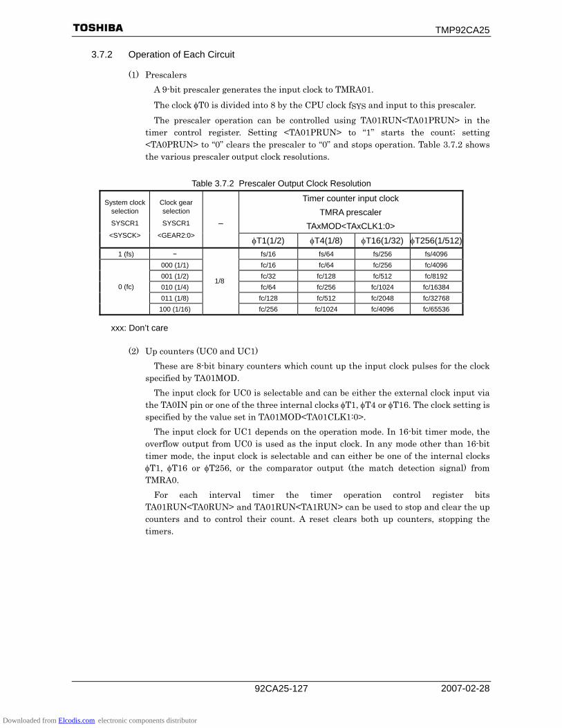
TMP92CA25
2007-02-28 92CA25-127
3.7.2 Operation of Each Circuit
(1) Prescalers A 9-bit prescaler generates the input clock to TMRA01. The clock φT0 is divided into 8 by the CPU clock fSYS and input to this prescaler. The prescaler operation can be controlled using TA01RUN<TA01PRUN> in the
timer control register. Setting <TA01PRUN> to “1” starts the count; setting <TA0PRUN> to “0” clears the prescaler to “0” and stops operation. Table 3.7.2 shows the various prescaler output clock resolutions.
Table 3.7.2 Prescaler Output Clock Resolution
Timer counter input clock TMRA prescaler
TAxMOD<TAxCLK1:0>
System clock selection
SYSCR1
<SYSCK>
Clock gear selection
SYSCR1
<GEAR2:0>
−
φT1(1/2) φT4(1/8) φT16(1/32) φT256(1/512)1 (fs) − fs/16 fs/64 fs/256 fs/4096
000 (1/1) fc/16 fc/64 fc/256 fc/4096 001 (1/2) fc/32 fc/128 fc/512 fc/8192 010 (1/4) fc/64 fc/256 fc/1024 fc/16384 011 (1/8) fc/128 fc/512 fc/2048 fc/32768
0 (fc)
100 (1/16)
1/8
fc/256 fc/1024 fc/4096 fc/65536
xxx: Don’t care
(2) Up counters (UC0 and UC1) These are 8-bit binary counters which count up the input clock pulses for the clock
specified by TA01MOD. The input clock for UC0 is selectable and can be either the external clock input via
the TA0IN pin or one of the three internal clocks φT1, φT4 or φT16. The clock setting is specified by the value set in TA01MOD<TA01CLK1:0>.
The input clock for UC1 depends on the operation mode. In 16-bit timer mode, the overflow output from UC0 is used as the input clock. In any mode other than 16-bit timer mode, the input clock is selectable and can either be one of the internal clocks φT1, φT16 or φT256, or the comparator output (the match detection signal) from TMRA0.
For each interval timer the timer operation control register bits TA01RUN<TA0RUN> and TA01RUN<TA1RUN> can be used to stop and clear the up counters and to control their count. A reset clears both up counters, stopping the timers.
Downloaded from Elcodis.com electronic components distributor

TMP92CA25
2007-02-28 92CA25-128
(3) Timer registers (TA0REG and TA1REG) These are 8-bit registers, which can be used to set a time interval. When the value
set in the timer register TA0REG or TA1REG matches the value in the corresponding up counter, the comparator match detect signal goes Active. If the value set in the timer register is 00H, the signal goes Active when the up counter overflows.
TA0REG has a double buffer structure, making a pair with the register buffer. The setting of the bit TA01RUN<TA0RDE> determines whether TA0REG’s double
buffer structure is enabled or disabled. It is disabled if <TA0RDE> = “0” and enabled if <TA0RDE> = “1”.
When the double buffer is enabled, data is transferred from the register buffer to the timer register when a 2n overflow occurs in PWM mode, or at the start of the PPG cycle in PPG mode. Hence the double buffer cannot be used in timer mode.
A reset initializes <TA0RDE> to “0”, disabling the double buffer. To use the double buffer, write data to the timer register, set <TA0RDE> to “1”, and write the following data to the register buffer. Figure 3.7.3 show the configuration of TA0REG.
Figure 3.7.3 Configuration of TA0REG
Note: The same memory address is allocated to the timer register and the register buffer. When <TA0RDE> = 0, the same value is written to the register buffer and the timer register; when <TA0RDE> = 1, only the register buffer is written to.
The address of each timer register is as follows.
TA0REG: 001102H TA1REG: 001103H TA2REG: 00110AH TA3REG: 00110BH
All these registers are write only and cannot be read.
Internal data bus
Timer registers 0 (TA0REG)
Register buffers 0
Shift trigger B
Selector
S A
Write
Write to TA0REG
Matching detection PPG cycle2n overflow of PWM
TA01RUN<TA0RDE>
Downloaded from Elcodis.com electronic components distributor
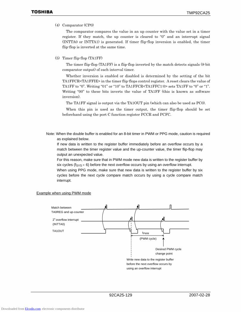
TMP92CA25
2007-02-28 92CA25-129
(4) Comparator (CP0) The comparator compares the value in an up counter with the value set in a timer
register. If they match, the up counter is cleared to “0” and an interrupt signal (INTTA0 or INTTA1) is generated. If timer flip-flop inversion is enabled, the timer flip-flop is inverted at the same time.
(5) Timer flip-flop (TA1FF)
The timer flip-flop (TA1FF) is a flip-flop inverted by the match detects signals (8-bit comparator output) of each interval timer.
Whether inversion is enabled or disabled is determined by the setting of the bit TA1FFCR<TA1FFIE> in the timer flip-flops control register. A reset clears the value of TA1FF to “0”. Writing “01” or “10” to TA1FFCR<TA1FFC1:0> sets TA1FF to “0” or “1”. Writing “00” to these bits inverts the value of TA1FF (this is known as software inversion).
The TA1FF signal is output via the TA1OUT pin (which can also be used as PC0). When this pin is used as the timer output, the timer flip-flop should be set
beforehand using the port C function register PCCR and PCFC.
Note: When the double buffer is enabled for an 8-bit timer in PWM or PPG mode, caution is required as explained below. If new data is written to the register buffer immediately before an overflow occurs by a match between the timer register value and the up-counter value, the timer flip-flop may output an unexpected value. For this reason, make sure that in PWM mode new data is written to the register buffer by six cycles (fSYS × 6) before the next overflow occurs by using an overflow interrupt. When using PPG mode, make sure that new data is written to the register buffer by six cycles before the next cycle compare match occurs by using a cycle compare match interrupt.
Example when using PWM mode
TA1OUT
2n overflow interrupt (INTTA0)
tPWM
(PWM cycle)
Match between TA0REG and up-counter
Desired PWM cycle change point
Write new data to the register buffer before the next overflow occurs by using an overflow interrupt
Downloaded from Elcodis.com electronic components distributor

TMP92CA25
2007-02-28 92CA25-130
3.7.3 SFR
TMRA01 Run Register 7 6 5 4 3 2 1 0
Bit symbol TA0RDE I2TA01 TA01PRUN TA1RUN TA0RUNTA01RUN (1100H) Read/Write R/W R/W After reset 0 0 0 0 0
TMRA01 prescaler
UP counter (UC1)
UP counter (UC0)
Function Double buffer 0: Disable 1: Enable
IDLE2 0: Stop 1: Operate 0: Stop and clear
1: Run (Count up)
Note: The values of bits 4 to 6 of TA01RUN are undefined when read.
TMRA23 Run Register 7 6 5 4 3 2 1 0
Bit symbol TA2RDE I2TA23 TA23PRUN TA3RUN TA2RUNTA23RUN (1108H) Read/Write R/W R/W After reset 0 0 0 0 0
TMRA23 prescaler
UP counter (UC3)
UP counter (UC4)
Function Double buffer 0: Disable 1: Enable
IDLE2 0: Stop 1: Operate 0: Stop and clear
1: Run (Count up)
Note: The values of bits 4 to 6 of TA23RUN are undefined when read.
Figure 3.7.4 TMRA01 Run Register and TMRA23 Run Register
Timer run/stop control 0 Stop and clear 1 Run (Count up)
TA0REG double buffer control 0 Disable 1 Enable
Timer run/stop control 0 Stop and clear 1 Run (Count up)
TA2REG double buffer control 0 Disable 1 Enable
Downloaded from Elcodis.com electronic components distributor
TMP92CA25
2007-02-28 92CA25-131
TMRA01 Mode Register 7 6 5 4 3 2 1 0
Bit symbol TA01M1 TA01M0 PWM01 PWM00 TA1CLK1 TA1CLK0 TA0CLK1 TA0CLK0TA01MOD (1104H) Read/Write R/W After reset 0 0 0 0 0 0 0 0 Function Operation mode
00: 8-bit timer mode 01: 16-bit timer mode 10: 8-bit PPG mode 11: 8-bit PWM mode
PWM cycle 00: Reserved 01: 26 10: 27 11: 28
Source clock for TMRA1 00: TA0TRG 01: φT1 10: φT16 11: φT256
Source clock for TMRA000: Reserved 01: φT1 10: φT4 11: φT16
TMRA0 source clock selection 00 (Reserved) 01 φT1 (Prescaler) 10 φT4 (Prescaler) 11 φT16 (Prescaler)
TMRA1 source clock selection TA01MOD
<TA01M1:0> ≠ 01 TA01MOD <TA01M1:0> = 01
00 Comparator output from TMRA0
01 φT1 10 φT16 11 φT256
Overflow output from TMRA0 (16-bit timer mode)
PWM cycle selection
00 Reserved 01 26× Source clock 10 27 × Source clock 11 28 × Source clock
TMRA01 operation mode selection
00 8-bit timers × 2ch 01 16-bit timer 10 8-bit PPG 11 8-bit PWM (TMRA0)
8-bit timer (TMRA1)
Figure 3.7.5 TMRA Mode Register
Downloaded from Elcodis.com electronic components distributor

TMP92CA25
2007-02-28 92CA25-132
TMRA23 Mode Register 7 6 5 4 3 2 1 0
Bit symbol TA23M1 TA23M0 PWM21 PWM20 TA3CLK1 TA3CLK0 TA2CLK1 TA2CLK0TA23MOD (110CH) Read/Write R/W After reset 0 0 0 0 0 0 0 0 Function Operation mode
00: 8-bit timer mode 01: 16-bit timer mode 10: 8-bit PPG mode 11: 8-bit PWM mode
PWM cycle 00: Reserved 01: 26 10: 27 11: 28
Source clock for TMRA3 00: TA2TRG 01: φT1 10: φT16 11: φT256
Source clock for TMRA200: Reserved 01: φT1 10: φT4 11: φT16
TMRA2 source clock selection 00 (Reserved) 01 φT1 (Prescaler) 10 φT4 (Prescaler) 11 φT16 (Prescaler)
TMRA3 source clock selection TA23MOD
<TA23M1:0> ≠ 01 TA23MOD <TA23M1:0> = 01
00 Comparator output from TMRA2
01 φT1 10 φT16 11 φT256
Overflow output from TMRA2 (16-bit timer mode)
PWM cycle selection
00 Reserved 01 26 × Source clock 10 27 × Source clock 11 28 × Source clock
TMRA23 operation mode selection
00 8-bit timers × 2ch 01 16-bit timer 10 8-bit PPG 11 8-bit PWM (TMRA2)
8-bit timer (TMRA3)
Figure 3.7.6 TMRA23 Mode Register
Downloaded from Elcodis.com electronic components distributor

TMP92CA25
2007-02-28 92CA25-133
TMRA1 Flip-Flop Control Register
7 6 5 4 3 2 1 0 Bit symbol TA1FFC1 TA1FFC0 TA1FFIE TA1FFISTA1FFCR
(1105H) Read/Write R/W After reset 1 1 0 0 Read-modify-write instruction is prohibited.
Function 00: Invert TA1FF 01: Set TA1FF 10: Clear TA1FF 11: Don’t care
TA1FF control for inversion 0: Disable 1: Enable
TA1FF inversion select 0: TMRA01: TMRA1
Inverse signal for timer flop-flop 1 (TA1FF) (Don’t care except in 8-bit timer mode)
0 Inversion by TMRA0 1 Inversion by TMRA1
Inversion of TA1FF 0 Disabled 1 Enabled
Control of TA1FF 00 Inverts the value of TA1FF 01 Sets TA1FF to “1” 10 Clears TA1FF to “0” 11 Don’t care
Note: The values of bits4 to 6 of TA1FFCR are undefined when read.
Figure 3.7.7 TMRA Flip-Flop Control Register
Downloaded from Elcodis.com electronic components distributor

TMP92CA25
2007-02-28 92CA25-134
TMRA3 Flip-Flop Control Register
7 6 5 4 3 2 1 0 Bit symbol TA3FFC1 TA3FFC0 TA3FFIE TA3FFISTA3FFCR
(110DH) Read/Write R/W After reset 1 1 0 0 Read- modify- write instruction is prohibited.
Function 00: Invert TA3FF 01: Set TA3FF 10: Clear TA3FF 11: Don’t care
TA3FF control for inversion 0: Disable 1: Enable
TA3FF inversion select 0: TMRA21: TMRA3
Inverse signal for timer flip-flop 3 (TA3FF) (Don’t care except in 8-bit timer mode)
0 Inversion by TMRA2 1 Inversion by TMRA3
Inversion of TA3FF 0 Disabled 1 Enabled
Control of TA3FF 00 Inverts the value of TA3FF 01 Sets TA3FF to “1” 10 Clears TA3FF to “0” 11 Don’t care
Note: The values of bits4 to 6 of TA3FFCR are undefined when read.
Figure 3.7.8 TMRA3 Flip-Flop Control Register
Downloaded from Elcodis.com electronic components distributor
TMP92CA25
2007-02-28 92CA25-135
TMRA Register
Symbol Address 7 6 5 4 3 2 1 0 −
W TA0REG 1102H
Undefined
− W TA1REG 1103H
Undefined
− W TA2REG 110AH
Undefined
− W TA3REG 110BH
Undefined
Note: Read-modify-write instruction is prohibited.
Figure 3.7.9 8-Bit Timers Register
Downloaded from Elcodis.com electronic components distributor
TMP92CA25
2007-02-28 92CA25-136
3.7.4 Operation in Each Mode
(1) 8-bit timer mode Both TMRA0 and TMRA1 can be used independently as 8-bit interval timers.
1. Generating interrupts at a fixed interval (using TMRA1) To generate interrupts at constant intervals using TMRA1 (INTTA1), first stop
TMRA1 then set the operation mode, input clock and a cycle to TA01MOD and TA1REG register, respectively. Then, enable the interrupt INTTA1 and start TMRA1 counting.
Example: To generate an INTTA1 interrupt every 40 μs at fC = 40 MHz, set each register as follows:
MSB LSB 7 6 5 4 3 2 1 0 TA01RUN ← − X X X − − 0 − Stop TMRA1 and clear it to “0”. TA01MOD ← 0 0 X X 0 1 − − Select 8-bit timer mode and select φT1 (= (16/fc)s at fC =
40 MHz) as the input clock. TA1REG ← 0 1 1 0 0 1 0 0 Set TREG1 to 40 μs ÷ φT1 = 100 = 64H. INTETA01 ← X 1 0 1 − − − − Enable INTTA1 and set it to level 5. TA01RUN ← – X X X − 1 1 − Start TMRA1 counting.
X: Don’t care, −: No change
Select the input clock using Table 3.7.3.
Table 3.7.3 Selecting Interrupt Interval and the Input Clock Using 8-Bit Timer
Input Clock Interrupt Interval (at fSYS = 20 MHz) Resolution φT1 (8/fSYS) 0.4 μs to 102.4 μs 0.4 μs φT4 (32/fSYS) 1.6 μs to 409.6 μs 1.6 μs φT16 (128/fSYS) 6.4 μs to 1.638 ms 6.4 μs φT256 (2048/fSYS) 102.4 μs to 26.21 ms 102.4 μs
Note: The input clocks for TMRA0 and TMRA1 differ as follows: TMRA0: Uses TMRA0 input (TA0IN) and can be selected from φT1, φT4 or φT16 TMRA1: Matches output of TMRA0 (TA0TRG) and can be selected from φT1, φT16, φT256
Downloaded from Elcodis.com electronic components distributor
TMP92CA25
2007-02-28 92CA25-137
2. Generating a 50 % duty ratio square wave pulse The state of the timer flip-flop (TA1FF1) is inverted at constant intervals and
its status output via the timer output pin (TA1OUT).
Example: To output a 2.4-μs square wave pulse from the TA1OUT pin at fC = 40 MHz, use the following procedure to make the appropriate register settings. This example uses TMRA1; however, either TMRA0 or TMRA1 may be used.
7 6 5 4 3 2 1 0 TA01RUN ← − X X X − − 0 − Stop TMRA1 and clear it to “0”. TA01MOD ← 0 0 X X 0 1 − − Select 8-bit timer mode and select φT1 (= (16/fc)s at fC =
40 MHz) as the input clock. TA1REG ← 0 0 0 0 0 0 1 1 Set the timer register to 2.4 μs ÷ φT1 ÷ 2 = 3 TA1FFCR ← X X X X 1 0 1 1 Clear TA1FF to “0” and set it to invert on the match detect
signal from TMRA1. PCCR ← − − − − − − − 1 PCFC ← − − − − − − − 1
Set PC0 to function as the TA1OUT pin.
TA01RUN ← − X X X − 1 1 − Start TMRA1 counting. X: Don’t care, −: No change
Figure 3.7.10 Square Wave Output Timing Chart (50 % Duty)
0 1 2 3 0 1 2 3 0 1 2 3 0
φT1
TA01RUN <TA01RUN>
Bit7 to Bit2
Bit1
Bit0
INTTA1
TA1FF
TA1OUT
Up counter
Comparatortiming
Comparator output(Match detect)
UC1 clear
1.2 μs at fC = 40 MHz
Downloaded from Elcodis.com electronic components distributor
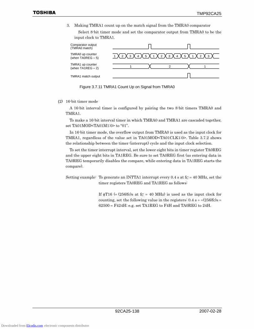
TMP92CA25
2007-02-28 92CA25-138
3. Making TMRA1 count up on the match signal from the TMRA0 comparator Select 8-bit timer mode and set the comparator output from TMRA0 to be the
input clock to TMRA1.
Figure 3.7.11 TMRA1 Count Up on Signal from TMRA0
(2) 16-bit timer mode A 16-bit interval timer is configured by pairing the two 8-bit timers TMRA0 and
TMRA1. To make a 16-bit interval timer in which TMRA0 and TMRA1 are cascaded together,
set TA01MOD<TA01M1:0> to “01”. In 16-bit timer mode, the overflow output from TMRA0 is used as the input clock for
TMRA1, regardless of the value set in TA01MOD<TA01CLK1:0>. Table 3.7.2 shows the relationship between the timer (interrupt) cycle and the input clock selection.
To set the timer interrupt interval, set the lower eight bits in timer register TA0REG and the upper eight bits in TA1REG. Be sure to set TA0REG first (as entering data in TA0REG temporarily disables the compare, while entering data in TA1REG starts the compare).
Setting example: To generate an INTTA1 interrupt every 0.4 s at fC = 40 MHz, set the
timer registers TA0REG and TA1REG as follows: If φT16 (= (256/fc)s at fC = 40 MHz) is used as the input clock for counting, set the following value in the registers: 0.4 s ÷ =(256/fc)s = 62500 = F424H; e.g. set TA1REG to F4H and TA0REG to 24H.
2 3 4 51 2 3 4 5 1 2 31
1 2 1
Comparator output (TMRA0 match)
TMRA0 up counter (when TA0REG = 5)
TMRA1 up counter (when TA1REG = 2)
TMRA1 match output
Downloaded from Elcodis.com electronic components distributor

TMP92CA25
2007-02-28 92CA25-139
The comparator match signal is output from TMRA0 each time the up counter UC0 matches TA0REG, though the up counter UC0 is not cleared.
In the case of the TMRA1 comparator, the match detect signal is output on each comparator pulse on which the values in the up counter UC1 and TA1REG match. When the match detect signal is output simultaneously from both the comparator TMRA0 and TMRA1, the up counters UC0 and UC1 are cleared to “0” and the interrupt INTTA1 is generated. Also, if inversion is enabled, the value of the timer flip-flop TA1FF is inverted.
Example: When TA1REG = 04H and TA0REG = 80H
Figure 3.7.12 Timer Output by 16-Bit Timer Mode
(3) 8-bit PPG (Programmable pulse generation) output mode Square wave pulses can be generated at any frequency and duty ratio by TMRA0.
The output pulses may be active low or active high. In this mode TMRA1 cannot be used.
TMRA0 outputs pulses on the TA1OUT pin (which can also be used as PC0).
Figure 3.7.13 8-Bit PPG Output Waveforms
Inversion
Value of up counter (UC1, UC0) TMRA0 comparator match detect signal
Interrupt INTTA1
0080H 0180H 0280H 0380H 0480H
Timer output TA1OUT
TMRA1 comparator match detect signal
Interrupt INTTA0
0080H
t
TA0REG
TA1REG
Example: <TA1FFC1:0> = “01”TA0REG and UC0 match (Interrupt INTTA0)
TA1REG and UC0 match (Interrupt INTTA1)
TA1OUT
tH tL
<TA1FFC1:0> = “10”
t
tL tH
<TA1FFC1:0> = “01”
Downloaded from Elcodis.com electronic components distributor
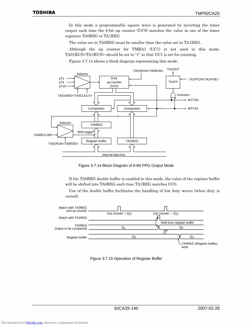
TMP92CA25
2007-02-28 92CA25-140
In this mode a programmable square wave is generated by inverting the timer output each time the 8-bit up counter (UC0) matches the value in one of the timer registers TA0REG or TA1REG.
The value set in TA0REG must be smaller than the value set in TA1REG. Although the up counter for TMRA1 (UC1) is not used in this mode,
TA01RUN<TA1RUN> should be set to “1” so that UC1 is set for counting. Figure 3.7.14 shows a block diagram representing this mode.
Figure 3.7.14 Block Diagram of 8-Bit PPG Output Mode
If the TA0REG double buffer is enabled in this mode, the value of the register buffer
will be shifted into TA0REG each time TA1REG matches UC0. Use of the double buffer facilitates the handling of low duty waves (when duty is
varied).
Figure 3.7.15 Operation of Register Buffer
Q2 Q1
Match with TA0REG and up counter
Match with TA1REG
Q3 Q2
(Up counter = Q1) (Up counter = Q2)
Shift from register buffer
TA0REG (Register buffer) write
TA0REG (Value to be compared)
Register buffer
8-bit
up counter (UC0)
Comparator Comparator
φT1 φT4 φT16
TA01MOD<TA0CLK1:0>
TA1FF
TA0REG
Register buffer TA1REG
TA01RUN<TA0RDE>
TA0REG-WR
TA01RUN<TA0RUN> TA1OUT
TA1FFCR<TA1FFIE>
INTTA0
INTTA1
Shift trigger
Internal data bus
Selector
Inversion
Selector
Downloaded from Elcodis.com electronic components distributor
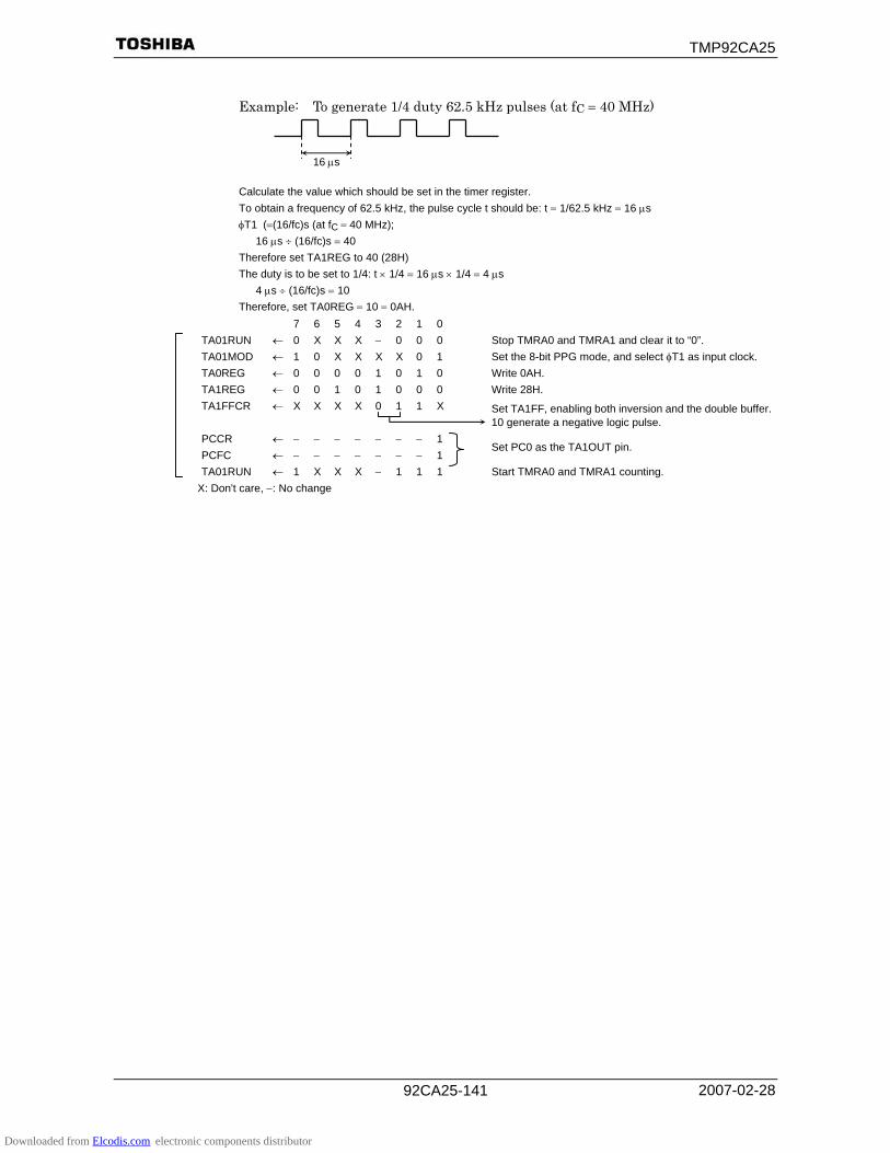
TMP92CA25
2007-02-28 92CA25-141
Example: To generate 1/4 duty 62.5 kHz pulses (at fC = 40 MHz)
Calculate the value which should be set in the timer register. To obtain a frequency of 62.5 kHz, the pulse cycle t should be: t = 1/62.5 kHz = 16 μs φT1 (=(16/fc)s (at fC = 40 MHz); 16 μs ÷ (16/fc)s = 40 Therefore set TA1REG to 40 (28H) The duty is to be set to 1/4: t × 1/4 = 16 μs × 1/4 = 4 μs 4 μs ÷ (16/fc)s = 10 Therefore, set TA0REG = 10 = 0AH.
7 6 5 4 3 2 1 0 TA01RUN ← 0 X X X − 0 0 0 Stop TMRA0 and TMRA1 and clear it to “0”. TA01MOD ← 1 0 X X X X 0 1 Set the 8-bit PPG mode, and select φT1 as input clock. TA0REG ← 0 0 0 0 1 0 1 0 Write 0AH. TA1REG ← 0 0 1 0 1 0 0 0 Write 28H. TA1FFCR ← X X X X 0 1 1 X Set TA1FF, enabling both inversion and the double buffer.
10 generate a negative logic pulse. PCCR ← − − − − − − − 1 PCFC ← − − − − − − − 1
Set PC0 as the TA1OUT pin.
TA01RUN ← 1 X X X − 1 1 1 Start TMRA0 and TMRA1 counting. X: Don't care, −: No change
16 μs
Downloaded from Elcodis.com electronic components distributor
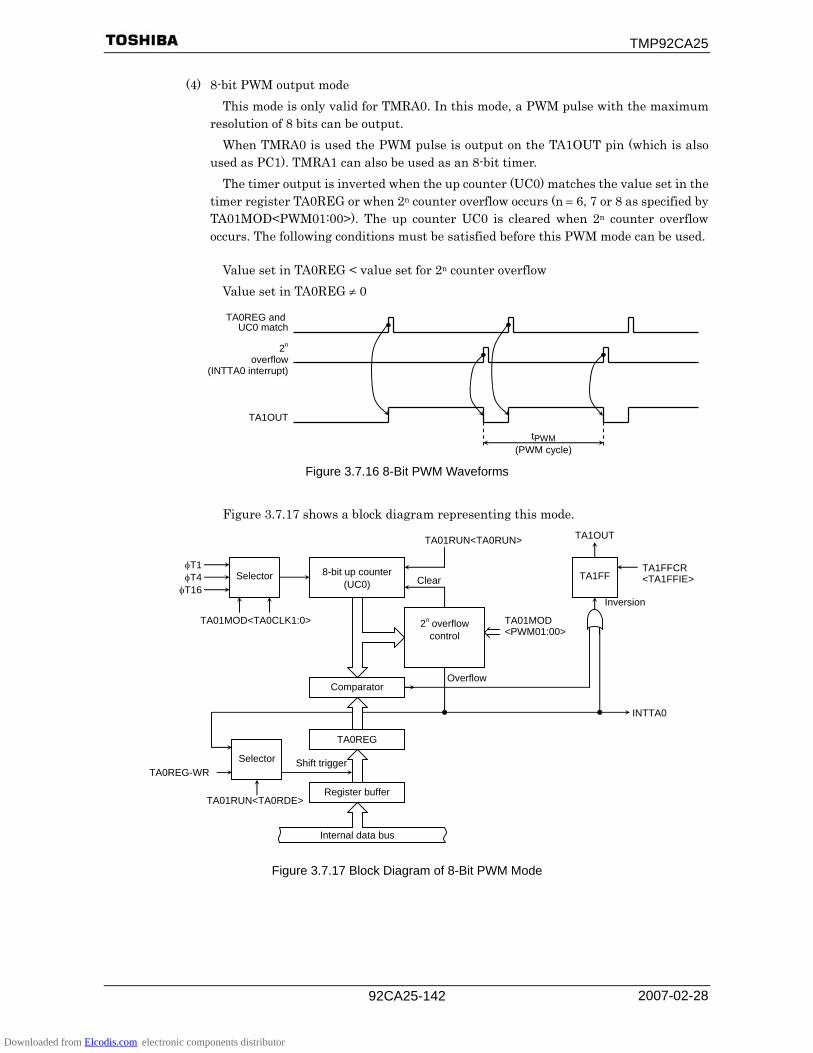
TMP92CA25
2007-02-28 92CA25-142
(4) 8-bit PWM output mode This mode is only valid for TMRA0. In this mode, a PWM pulse with the maximum
resolution of 8 bits can be output. When TMRA0 is used the PWM pulse is output on the TA1OUT pin (which is also
used as PC1). TMRA1 can also be used as an 8-bit timer. The timer output is inverted when the up counter (UC0) matches the value set in the
timer register TA0REG or when 2n counter overflow occurs (n = 6, 7 or 8 as specified by TA01MOD<PWM01:00>). The up counter UC0 is cleared when 2n counter overflow occurs. The following conditions must be satisfied before this PWM mode can be used.
Value set in TA0REG < value set for 2n counter overflow Value set in TA0REG ≠ 0
Figure 3.7.16 8-Bit PWM Waveforms
Figure 3.7.17 shows a block diagram representing this mode.
Figure 3.7.17 Block Diagram of 8-Bit PWM Mode
TA0REG and UC0 match
TA1OUT
tPWM (PWM cycle)
2n overflow
(INTTA0 interrupt)
Selector 8-bit up counter (UC0)
Comparator
φT1 φT4
φT16
TA01MOD<TA0CLK1:0>
TA1FF
TA0REG
Register buffer
Selector
TA01RUN<TA0RDE>
TA0REG-WR
TA01RUN<TA0RUN> TA1OUT
TA1FFCR <TA1FFIE>
Shift trigger
Internal data bus
Clear
2n overflow control
INTTA0
TA01MOD <PWM01:00>
Overflow
Inversion
Downloaded from Elcodis.com electronic components distributor

TMP92CA25
2007-02-28 92CA25-143
In this mode the value of the register buffer will be shifted into TA0REG if 2n
overflow is detected when the TA0REG double buffer is enabled. Use of the double buffer facilitates the handling of low duty ratio waves.
Figure 3.7.18 Register Buffer Operation
Example: To output the following PWM waves on the TA1OUT pin (at fC = 40 MHz).
To achieve a 51.2-μs PWM cycle by setting φT1 (= (16/fc)s (@fC = 40 MHz): 51.2 μs ÷ (16/fc)s = 128 2n= 128 Therefore n should be set to 7. Since the low level period is 36.0 μs when φT1 = (16/fc)s, set the following value for TREG0: 36.0 μs ÷ (16/fc)s = 90 = 5AH
MSB LSB 7 6 5 4 3 2 1 0 TA01RUN ← − X X X − − − 0 Stop TMRA0 and clear it to 0 TA01MOD ← 1 1 1 0 − − 0 1 Select 8-bit PWM mode (cycle: 27) and select φT1 as the
input clock. TA0REG ← 0 1 0 1 1 0 1 0 Write 5AH. TA1FFCR ← X X X X 1 0 1 X Clear TA1FF to 0; enable the inversion and double buffer. PCCR ← − − − − − − − 1 PCFC ← − − − − − − − 1
Set PC0 as the TA1OUT pin.
TA01RUN ← 1 X X X − 1 − 1 Start TMRA0 counting. X: Don't care, −: No change
Q2 Q1
Match with TA0REG
Q3 Q2
Up counter = Q1 Up counter = Q2
Shift into TA0REG
TA0REG (Register buffer) write
TA0REG (Value to be compared)
Register buffer
2n overflow
36.0 μs
51.2 μs
Downloaded from Elcodis.com electronic components distributor
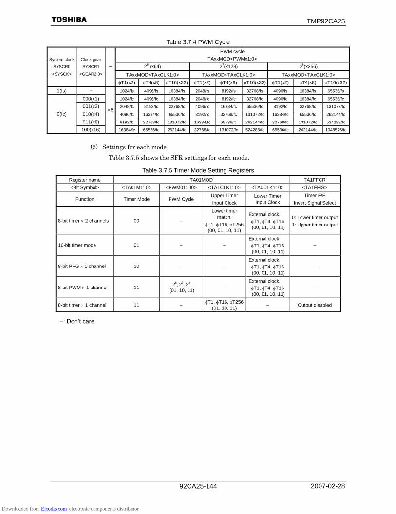
TMP92CA25
2007-02-28 92CA25-144
Table 3.7.4 PWM Cycle PWM cycle
TAxxMOD<PWMx1:0> 26 (x64) 27(x128) 28(x256)
TAxxMOD<TAxCLK1:0> TAxxMOD<TAxCLK1:0> TAxxMOD<TAxCLK1:0>
System clock
SYSCR0
<SYSCK>
Clock gear
SYSCR1
<GEAR2:0>
−
φT1(x2) φT4(x8) φT16(x32) φT1(x2) φT4(x8) φT16(x32) φT1(x2) φT4(x8) φT16(x32)
1(fs) − 1024/fs 4096/fs 16384/fs 2048/fs 8192/fs 32768/fs 4096/fs 16384/fs 65536/fs
000(x1) 1024/fc 4096/fc 16384/fc 2048/fc 8192/fc 32768/fc 4096/fc 16384/fc 65536/fc
001(x2) 2048/fc 8192/fc 32768/fc 4096/fc 16384/fc 65536/fc 8192/fc 32768/fc 131072/fc
010(x4) 4096/fc 16384/fc 65536/fc 8192/fc 32768/fc 131072/fc 16384/fc 65536/fc 262144/fc
011(x8) 8192/fc 32768/fc 131072/fc 16384/fc 65536/fc 262144/fc 32768/fc 131072/fc 524288/fc
0(fc)
100(x16)
×8
16384/fc 65536/fc 262144/fc 32768/fc 131072/fc 524288/fc 65536/fc 262144/fc 1048576/fc
(5) Settings for each mode
Table 3.7.5 shows the SFR settings for each mode.
Table 3.7.5 Timer Mode Setting Registers Register name TA01MOD TA1FFCR <Bit Symbol> <TA01M1: 0> <PWM01: 00> <TA1CLK1: 0> <TA0CLK1: 0> <TA1FFIS>
Function Timer Mode PWM Cycle Upper Timer Input Clock
Lower Timer Input Clock
Timer F/F Invert Signal Select
8-bit timer × 2 channels 00 −
Lower timer match,
φT1, φT16, φT256 (00, 01, 10, 11)
External clock, φT1, φT4, φT16 (00, 01, 10, 11)
0: Lower timer output1: Upper timer output
16-bit timer mode 01 − − External clock,
φT1, φT4, φT16 (00, 01, 10, 11)
−
8-bit PPG × 1 channel 10 − − External clock,
φT1, φT4, φT16 (00, 01, 10, 11)
−
8-bit PWM × 1 channel 11 26, 27, 28 (01, 10, 11) −
External clock, φT1, φT4, φT16 (00, 01, 10, 11)
−
8-bit timer × 1 channel 11 − φT1, φT16, φT256 (01, 10, 11) − Output disabled
−: Don’t care
Downloaded from Elcodis.com electronic components distributor

TMP92CA25
2007-02-28 92CA25-145
3.8 External Memory Extension Function (MMU)
By providing 3 local areas, the MMU function allows for the expansion of the program/data area up to 512 Mbytes.
The recommended address memory map is shown in Figure 3.8.1. However, when the memory used is less than 16 Mbytes, it is not necessary to set the MMU
register. In this case, please refer to the Memory Controller section. An area which can be set as a bank is called a local area. Since the address for local areas is
fixed, it cannot be changed. And, area which cannot be set as a bank is called Common area. Basically one series of program should be closed within one bank. Please don’t jump to the
same LOCAL-area in the different bank directly by JP instruction and so on. Refer to the examples as follows.
It is not possible for a program to branch between different banks of the same local area.
The TMP92CA25 has the following external pins for memory LSI connection.
Address bus: EA25, EA24 and A23 to A0 Chip select: CS0 to CS3 , CSZA to CSZF , SDCS ND0CE and ND1CE Data bus: D15 to D0
3.8.1 Recommended Memory Map
Figure 3.8.1 shows one recommended address memory map. This is for maximum expanded memory size and for a system in which an internal boot ROM with NAND flash is not required.
Downloaded from Elcodis.com electronic components distributor

TMP92CA25
2007-02-28 92CA25-146
Note: CSZA is a chip select for not only bank 0 to 15 of LOCAL-Z but also COMMON-Z.
Figure 3.8.1 Recommended Memory Map for Maximum Specification (Logical address)
Bank 0
000000H Address Memory Map
COMMON-X (2 Mbytes)
LOCAL-X (2 Mbytes)
LOCAL-Y (2 Mbytes)
COMMON-Y (2 Mbytes)
LOCAL-Z (4 Mbytes)
COMMON-Z (4 Mbytes)
Vector area
Internal I/O, RAM
200000H
400000H
600000H
800000H
C00000H
FFFF00H
FFFFFFH
1 2 3 15 31
Bank 0 1 2 3 15 31
CS0 area32 Mbytes
CS3 area4 Mbytes
CS1 area4 Mbytes
CS2 area8 Mbytes
Bank 0 1 2 3 15 3116 80 95
CE0ND pin (128 Mbytes)CE1ND pin (128 Mbytes)
Memory controller setting
3CS pin 64 Mbytes(2 Mbytes × 32)
SDCS or 1CS pin 64 Mbytes(2 Mbytes × 32)
CSZA pin (Note) 64 Mbytes(4 Mbytes × 16)
CSZB pin CSZF pin
: Internal area
: Overlapped with COMMON area and disabled setting as LOCAL area.
Downloaded from Elcodis.com electronic components distributor

TMP92CA25
2007-02-28 92CA25-147
Figure 3.8.2 Recommended Memory Map for Maximum Specification (Physical address)
000000H
Internal I/O and RAM
LOCAL-X 3CS
64 Mbytes
TMP92CA25
BANK 0
31
LOCAL-Y SDCS or 1CS
64 Mbytes
BANK 0
31
LOCAL-Z CSZA to CSZF , EA24, EA25 64 Mbytes × 6 = 384 Mbytes
BANK 0
15
BANK 48
63
CSZA CSZD
BANK 16
31
BANK 64
79
CSZB CSZE
BANK 32
47
BANK 80
95
CSZC CSZF
Downloaded from Elcodis.com electronic components distributor

TMP92CA25
2007-02-28 92CA25-148
3.8.2 Control Registers
There are 12 MMU registers, covering 4 functions (program, data read, data write and LCDC display data), in each of 3 local areas (Local-X, Y and Z), providing easy data access.
(Instructions for use) First, set the enable register and bank number for each LOCAL register. The relevant pin and memory settings should then be set to the ports and memory
controller. When the CPU or LCDC outputs a local area logical address, the MMU converts and
outputs this to the physical address according to the bank number. The physical address bus is output to the external address bus pin, thereby enabling access to external memory.
Note 1: Since the common area cannot be used as local area, do not set a bank number to LOCAL register which overlaps with the common area.
Note 2: Changing program BANK number (LOCALPX, Y or Z) is disabled in the LOCAL area. The program bank setting for each local area must be changed in the common area. (But bank setting of read data, write data and data for LCD display can be changed in the local area.)
Note 3: After data bank number register (LOCALRn, LOCALWn or LOCALLn; where “n” means X, Y or Z) is set by an instruction, do not access its memory by the following instruction because several clocks are required for effective MMU setting. For this reason, insert between them a dummy instruction which accesses SFR or another memory, as in the following example.
(Example) ld xix, 200000H ; ld (localrx), 81H ; Data bank number is set ld wa, (localrx) ; ← Inserted dummy instruction which accesses SFR ld wa, (xix) ; Instruction which reads BANK 1 of LOCAL-X area.
Note 4: When LOCAL-Z area is used, chip select signal CSZA should be assigned to P82 pin. In this case, CSZA works as chip select signal for not only BANK 0 to 15 but also COMMON-Z. The following setting after reset is required before setting Port82.
ld (localpz), 80H ; LOCAL-Z bank enable for program ld (localrz), 80H ; LOCAL-Z bank enable for data read ld (localwz), 80H ; LOCAL-Z bank enable for data write (*1) ld (locallz), 80H ; LOCAL-Z bank enable for LCD display memory (*2) ld (p8fc), − − − − − 0 − − B ; Set P82 pin to CSZA output ld (p8fc2), − − − − − 1 − − B ;
(*1) If COMMON-Z area is not used as data write memory, this setting is not required.
(*2) If COMMON-Z area is not used as LCD display memory, this setting is not required.
Downloaded from Elcodis.com electronic components distributor
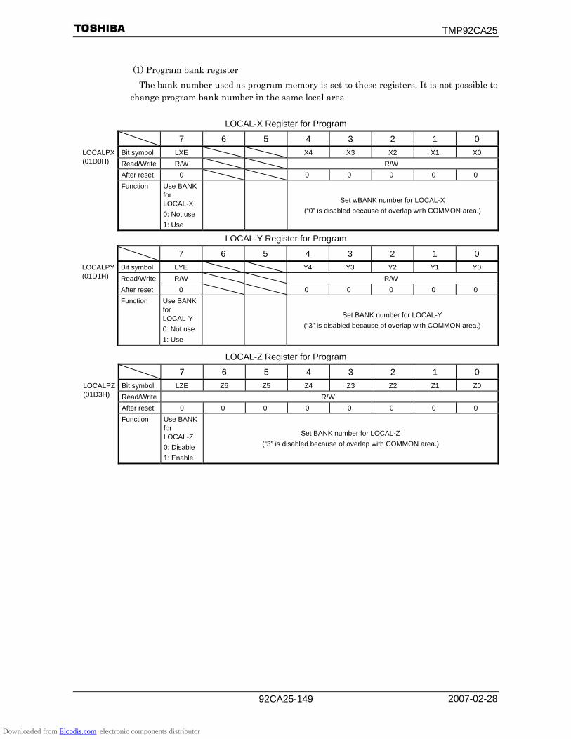
TMP92CA25
2007-02-28 92CA25-149
(1) Program bank register The bank number used as program memory is set to these registers. It is not possible to
change program bank number in the same local area.
LOCAL-X Register for Program
7 6 5 4 3 2 1 0 Bit symbol LXE X4 X3 X2 X1 X0 LOCALPX
(01D0H) Read/Write R/W R/W After reset 0 0 0 0 0 0 Function Use BANK
for LOCAL-X 0: Not use 1: Use
Set wBANK number for LOCAL-X
(“0” is disabled because of overlap with COMMON area.)
LOCAL-Y Register for Program
7 6 5 4 3 2 1 0 Bit symbol LYE Y4 Y3 Y2 Y1 Y0 LOCALPY
(01D1H) Read/Write R/W R/W After reset 0 0 0 0 0 0 Function Use BANK
for LOCAL-Y 0: Not use 1: Use
Set BANK number for LOCAL-Y (“3” is disabled because of overlap with COMMON area.)
LOCAL-Z Register for Program
7 6 5 4 3 2 1 0 Bit symbol LZE Z6 Z5 Z4 Z3 Z2 Z1 Z0 LOCALPZ
(01D3H) Read/Write R/W After reset 0 0 0 0 0 0 0 0 Function Use BANK
for LOCAL-Z 0: Disable 1: Enable
Set BANK number for LOCAL-Z (“3” is disabled because of overlap with COMMON area.)
Downloaded from Elcodis.com electronic components distributor

TMP92CA25
2007-02-28 92CA25-150
(2) LCD Display bank register The bank number used as LCD display memory is set to these registers. Since the bank
registers for CPU and LCDC are prepared independently, the bank number for CPU (Program, Read data or Write data) can be changed during LCD display.
LOCAL-X Register for LCDC Display Data
7 6 5 4 3 2 1 0 Bit symbol LXE X4 X3 X2 X1 X0 LOCALLX
(01D4H) Read/Write R/W R/W After reset 0 0 0 0 0 0 Function Use BANK
for LOCAL-X 0: Not use 1: Use
Set BANK number for LOCAL-X
(“0” is disabled because of overlap with COMMON area.)
LOCAL-Y Register for LCDC Display Data
7 6 5 4 3 2 1 0 Bit symbol LYE Y4 Y3 Y2 Y1 Y0 LOCALLY
(01D5H) Read/Write R/W R/W After reset 0 0 0 0 0 0 Function Use BANK
for LOCAL-Y 0: Not use 1: Use
Set BANK number for LOCAL-Y (“3” is disabled because of overlap with COMMON area.)
LOCAL-Z Register for LCDC Display Data
7 6 5 4 3 2 1 0 Bit symbol LZE Z6 Z5 Z4 Z3 Z2 Z1 Z0 LOCALLZ
(01D7H) Read/Write R/W After reset 0 0 0 0 0 0 0 0 Function Use BANK
for LOCAL-Z 0: Disable 1: Enable
Set BANK number for LOCAL-Z (“3” is disabled because of overlap with COMMON area.)
Downloaded from Elcodis.com electronic components distributor

TMP92CA25
2007-02-28 92CA25-151
(3) Read data bank register The bank register number used as read data memory is set to these registers. The
following is an example where the read data bank register of LOCAL-X is set to “1”. When “ld wa, (xix)” instruction is executed, the bank becomes effective only at the read cycle for xix address.
(Example) ld xix, 200000h ; ld (localrx), 81h ; Set Read data bank. ld wa, (localrx) ; <-- Insert dummy instruction which accesses
SFR ld wa, (xix) ; Read bank1 of LOCAL-X area
LOCAL-X Register for Read Data
7 6 5 4 3 2 1 0 Bit symbol LXE X4 X3 X2 X1 X0 LOCALRX
(01D8H) Read/Write R/W R/W After reset 0 0 0 0 0 0 Function Use BANK
for LOCAL-X 0: Not use 1: Use
Set BANK number for LOCAL-X
(“0” is disabled because of overlap with COMMON area.)
LOCAL-Y Register for Read Data
7 6 5 4 3 2 1 0 Bit symbol LYE Y4 Y3 Y2 Y1 Y0 LOCALRY
(01D9H) Read/Write R/W R/W After reset 0 0 0 0 0 0 Function Use BANK
for LOCAL-Y 0: Not use 1: Use
Set BANK number for LOCAL-Y (“3” is disabled because of overlap with COMMON area.)
LOCAL-Z Register for Read Data
7 6 5 4 3 2 1 0 Bit symbol LZE Z6 Z5 Z4 Z3 Z2 Z1 Z0 LOCALRZ
(01DBH) Read/Write R/W After reset 0 0 0 0 0 0 0 0 Function Use BANK
for LOCAL-Z 0: Disable 1: Enable
Set BANK number for LOCAL-Z (“3” is disabled because of overlap with COMMON area.)
Downloaded from Elcodis.com electronic components distributor
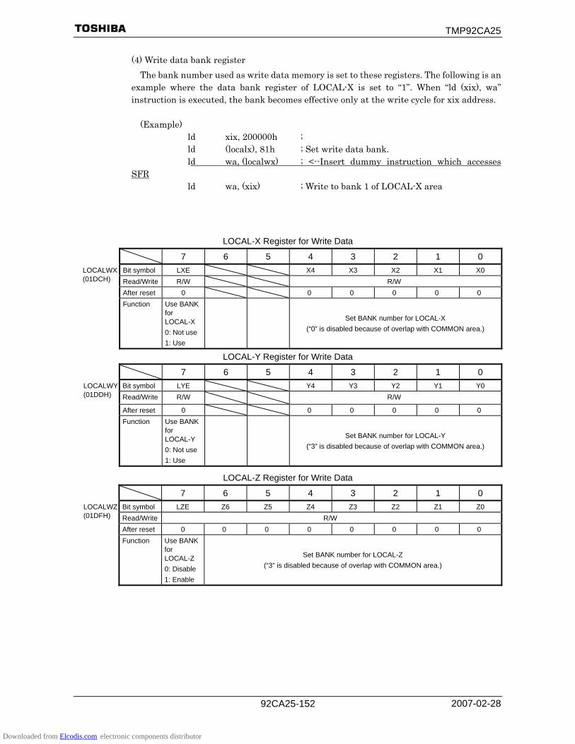
TMP92CA25
2007-02-28 92CA25-152
(4) Write data bank register The bank number used as write data memory is set to these registers. The following is an
example where the data bank register of LOCAL-X is set to “1”. When “ld (xix), wa” instruction is executed, the bank becomes effective only at the write cycle for xix address.
(Example) ld xix, 200000h ; ld (localx), 81h ; Set write data bank. ld wa, (localwx) ; <--Insert dummy instruction which accesses
SFR ld wa, (xix) ; Write to bank 1 of LOCAL-X area
LOCAL-X Register for Write Data
7 6 5 4 3 2 1 0 Bit symbol LXE X4 X3 X2 X1 X0 LOCALWX
(01DCH) Read/Write R/W R/W After reset 0 0 0 0 0 0 Function Use BANK
for LOCAL-X 0: Not use 1: Use
Set BANK number for LOCAL-X
(“0” is disabled because of overlap with COMMON area.)
LOCAL-Y Register for Write Data
7 6 5 4 3 2 1 0 Bit symbol LYE Y4 Y3 Y2 Y1 Y0 LOCALWY
(01DDH) Read/Write R/W R/W
After reset 0 0 0 0 0 0 Function Use BANK
for LOCAL-Y 0: Not use 1: Use
Set BANK number for LOCAL-Y (“3” is disabled because of overlap with COMMON area.)
LOCAL-Z Register for Write Data
7 6 5 4 3 2 1 0 Bit symbol LZE Z6 Z5 Z4 Z3 Z2 Z1 Z0 LOCALWZ
(01DFH) Read/Write R/W After reset 0 0 0 0 0 0 0 0 Function Use BANK
for LOCAL-Z 0: Disable 1: Enable
Set BANK number for LOCAL-Z (“3” is disabled because of overlap with COMMON area.)
Downloaded from Elcodis.com electronic components distributor

TMP92CA25
2007-02-28 92CA25-153
3.8.3 Setting Example
Below is a setting example.
No. Used as Memory Setting MMU AreaLogical Address
Physical Address
(a) Main
routine COMMON-Z
C00000H to FFFFFFH
(b) Character
ROM
NOR flash (16 Mbytes,
1 pcs)
CSZA , 32 bits, 1 wait Bank 0 in
LOCAL-Z 800000H to BFFFFFH
000000H to3FFFFFH
(c) Sub
routine Bank 0 in LOCAL-Y
000000H to1FFFFFH
(d) LCD
display RAM
SRAM (16 Mbytes,
1 pcs)
1CS , 16 bits, 0 waits Bank 1 in
LOCAL-Y
400000H to 5FFFFFH
200000H to3FFFFFH
(e) Stack RAM
Internal RAM(16 Kbytes)
− (32 bits, 1 clock) − 002000H to 005FFFH
(a) Main routine (COMMON-Z)
Logical Address
Physical Address
No Instruction Comment
1 org C00000H ; C00000H ← (Same) 2 ldw (mamr2), 80FFH ; CS2 800000-FFFFFF/8 Mbytes C000xxH ← 3 ldw (b2csl), C222H ; CS2 32-bit ROM, 1 wait 4 ldw (mamr1), 40FFH ; CS1 400000-7FFFFF/4 Mbytes
5 ldw (b1csl), 8111H ; CS1 16-bit RAM, 0 waits 5.1 ld (localpz), 80H ; LOCAL-Z bank enable for program
5.2 ld (localrz), 80H ; LOCAL-Z bank enable for data read 6 ld (p8fc), 02H ; P81: 1CS 7 ld (p8fc2), 04H ; P82: CSZA 8 ld (pjfc), 07H ; PJ2: SRWR , PJ1: SRLUB , PJ0: SRLLB 9 ld xsp, 6000H ; Stack pointer = 6000H 10 ld (localpy), 80H ; BANK 0 in LOCAL-Y is set as program for
sub routine 11 : ; C000yyH ← 12 call 400000H ; Call sub routine 13 : ; 14 : ; 15 : ;
• Instructions from No.2 to No.8 are settings for ports and memory controller.
• No.9 is a setting for stack pointer. It is assigned to internal RAM.
• No.10 is a setting to execute No.12’s instruction.
• No.12 is an instruction to call sub routine. When CPU outputs 400000H address, this MMU will convert and output 000000H address to external address bus: A23 to A0. And CS1 for SRAM will be asserted because its logical address is in the CS1area at the same time. These instructions allow the CPU to branch to sub routine.
Note:This example assumes a sub routine program is already written on SRAM.
Downloaded from Elcodis.com electronic components distributor

TMP92CA25
2007-02-28 92CA25-154
(b) Sub routine (Bank 0 in LOCAL-Y)
Logical Address
Physical Address
No Instruction Comment
16 org 400000H ; 400000H 000000H 17 ld (localwy), 81H ; BANK 1 in LOCAL-Y is set as write data for
LCD display RAM 4000xxH 0000xxH 18 ld (locally), 81H ; BANK 1 in LOCAL-Y is set as LCD display data
for LCD display RAM 19 ld (localrz), 80H ; BANK 0 in LOCAL-Z is set as read data for
character ROM 20 ld xiy, 800000H ; Index address register to read character ROM 21 ld wa, (xiy) ; Reading character ROM 22 : ; Convert it to display data 23 ld (localpy), 82H ; 24 ld xix, 400000H ; Index address register to write LCD
display data 25 ld (xix), bc ; Writing LCD display data 26 : ; Setting LCD controller 27 : ; 28 ld xiz, 400000H ; Setting LCD start address to LCDC 29 ld (lsarcl), xiz ; 30 ld (lcdctl0), 01H ; Start LCD display operation 31 : ; 5000yyH 1000yyH 32 ret ;
• No.17 and No.18 are settings for BANK 1 of LOCAL-Y. In this case, LCD display data is written to SRAM by CPU. So, (LOCALWY) and (LOCALLY) should be set to the same BANK 1.
• No.19 is a setting for BANK 0 of LOCAL-Z to read data from character ROM.
• No.20 and No.21 are instructions to read data from character ROM. When CPU outputs 800000H address, this MMU will convert and output 000000H address to external address bus: A23 to A0. And CSZA for NOR flash will be asserted because its logical address is in the CS2 area at the same time. These instructions allow the CPU to read data from character ROM.
• No.23 is an instruction which changes the program BANK number in the local area. This setting is disabled.
• No.24 and No.25 are instructions to write data to SRAM. When CPU outputs 400000H address, this MMU will convert and output 200000H address to external address bus: A23 to A0. And CS1 for SRAM will be asserted because its logical address is in the CS1area at the same time. These instructions allow the CPU to write data to SRAM.
• No.28 and No.29 are settings to set LCD starting address to LCD controller. When LCDC outputs 400000H address in DMA cycle, this MMU will convert and output 200000H address to external address bus: A23 to A0. And CS1 for SRAM will be asserted because its logical address is in the CS1 area at the same time. These instructions allow the LCDC to read data from SRAM.
• No.30 is an instruction to start LCD display operation.
Downloaded from Elcodis.com electronic components distributor

TMP92CA25
2007-02-28 92CA25-155
3.9 Serial Channels
The TMP92CA25 includes 1 serial I/O channels. For the channel, either UART mode (asynchronous transmission) or I/O interface mode (synchronous transmission) can be selected. And SIO0 includes data modulator that supports the IrDA 1.0 infrared data communication specification.
I/O interface mode Mode 0: For transmitting and receiving I/O data using the
synchronizing signal SCLK for extending I/O. UART mode Mode 1: 7-bit data
Mode 2: 8-bit data Mode 3: 9-bit data
In mode 1 and mode 2 a parity bit can be added. Mode 3 has a wakeup function for making the
master controller start slave controllers via a serial link (a multi controller system). Figure 3.9.2 is block diagrams for SIO0. SIO0 is compounded mainly prescaler, serial clock generation circuit, receiving buffer and
control circuit, transmission buffer and control circuit. This chapter contains the following sections:
3.9.1 Block diagram 3.9.2 Operation of each circuit 3.9.3 SFR 3.9.4 Operation in each mode 3.9.5 Support for IrDA mode
Downloaded from Elcodis.com electronic components distributor
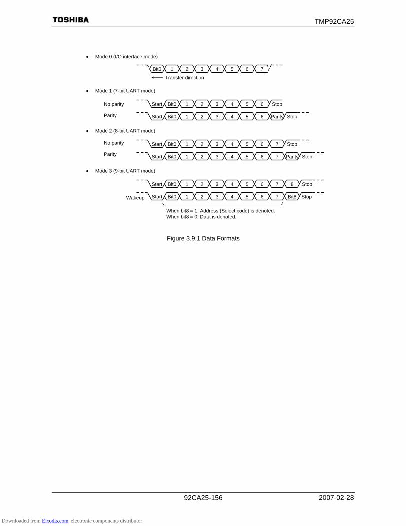
TMP92CA25
2007-02-28 92CA25-156
Figure 3.9.1 Data Formats
Bit0 1 2 3 4 5 6 7
Bit0 1 2 3 4 5 6 Stop Start
Bit0 1 2 3 4 5 Parity Stop Start 6
Bit0 1 2 3 4 5 7 Stop Start
Bit0 1 2 3 4 5 Parity Stop Start 7
6
6
Bit0 1 2 3 4 5 8 Stop Start
Bit0 1 2 3 4 5 Stop Start Bit8
6
6
7
7
Transfer direction
• Mode 0 (I/O interface mode)
• Mode 1 (7-bit UART mode)
No parity
Parity
No parity
Parity
• Mode 2 (8-bit UART mode)
• Mode 3 (9-bit UART mode)
When bit8 = 1, Address (Select code) is denoted.When bit8 = 0, Data is denoted.
Wakeup
Downloaded from Elcodis.com electronic components distributor

TMP92CA25
2007-02-28 92CA25-157
3.9.1 Block Diagrams
Figure 3.9.2 Block Diagram of Serial Channel 0
Sel
ecto
r φT0 φT2 φT8 φT32
SC0MOD0<SC1:0>
Receive buffer 1 (Shift register)
RXDCLK
SC0MOD0 <CTSE>
Pre
scal
er
Sel
ecto
r
TA0TRG (from TMRA0)
UARTmode
BR0CR <BR0S3:0>
Baud rate generator
Sel
ecto
r
SC0MOD0<SM1:0>
Sel
ecto
r ÷2
I/O interface mode
SC0CR<IOC>
Receive counter (UART only ÷ 16)
Transmision counter
(UART only ÷ 16)
Receive control
Transmission control
INTRX0 INTTX0
Receive buffer 2 (SC0BUF)RB8 Error flag
SC0CR <OERR> <PERR> <FERR>
Serial channelinterrupt control
TB8
CTS0
TXD0 Transmission buffer (SC0BUF)
RXD0
TXDCLK
SC0MOD0<WU>
fIO
SC0MOD0 <RXE>
SCLK0
SCLK0
SIOCLK
Internal data bus
Parity control
SC0CR <PE> <EVEN>
Serial clock generation circuit
BR0CR<BR0CK1:0>
BR0ADD <BR0K3:0>
BR0CR <BR0ADDE>
I/O interface mode
φT0 2 64 4 8 16 32
Prescaler
φT2 φT8 φT32
INT request
Downloaded from Elcodis.com electronic components distributor

TMP92CA25
2007-02-28 92CA25-158
3.9.2 Operation for Each Circuit
(1) SIO Prescaler and prescaler clock select There is a 6-bit prescaler for waking serial clock. The prescaler can be run by selecting the baud rate generator as the waking serial
clock. Table 3.9.1 shows prescaler clock resolution into the baud rate generator.
Table 3.9.1 Prescaler Clock Resolution to Baud Rate Generator Baud rate generator input clock
SIO prescaler BR0CR<BR0CK1:0>
System clock selection
SYSCR1
<SYSCK>
Clock gear selection SYSCR1
<GEAR2:0>
−
φT0 φT2(1/4) φT8(1/16) φT32(1/64) 1(fs) − fs/8 fs/32 fs/128 fs/512
000(1/1) fc/8 fc/32 fc/128 fc/512 001(1/2) fc/16
fc/64 fc/256 fc/1024
010(1/4) fc/32
fc/128 fc/512 fc/2048 011(1/8) fc/64
fc/256 fc/1024 fc/4096
0(fc)
100(1/16)
1/8
fc/128 fc/512 fc/2048 fc/8192
The baud rate generator selects between 4 clock inputs: φT0, φT2, φT8, and φT32 among the prescaler outputs.
Downloaded from Elcodis.com electronic components distributor
TMP92CA25
2007-02-28 92CA25-159
(2) Baud rate generator The baud rate generator is a circuit which generates transmission and receiving
clocks that determine the transfer rate of the serial channels. The input clock to the baud rate generator, φT0, φT2, φT8 or φT32, is generated by
the 6-bit SIO prescaler, which is shared by the timers. One of these input clocks is selected using the BR0CR<BR0CK1:0> field in the baud rate generator control register.
The baud rate generator includes a frequency divider, which divides the frequency by 1 or N + (16 − K)/16 or 16 values, thereby determining the transfer rate.
The transfer rate is determined by the settings of BR0CR<BR0ADDE, BR0S3:0> and BR0ADD<BR0K3:0>.
• In UART mode (1) When BR0CR<BR0ADDE> = 0
The settings BR0ADD<BR0K3:0> are ignored. The baud rate generator divides the selected prescaler clock by N, which is set in BR0CK<BR0S3:0>. (N = 1, 2, 3 …16)
(2) When BR0CR<BR0ADDE> = 1 The N + (16 − K)/16 division function is enabled. The baud rate generator
divides the selected prescaler clock by N + (16 − K)/16 using the value of N set in BR0CR<BR0S3:0> (N = 2, 3…15) and the value of K set in BR0ADD<BR0K3:0> (K = 1, 2, 3…15)
Note: If N = 1 or N = 16, the N + (16 − K)/16 division function is disabled. Set BR0CR<BR0ADDE> to 0.
• In I/O interface mode The N + (16 − K)/16 division function is not available in I/O interface mode. Set
BR0CR<BR0ADDE> to 0 before dividing by N. The method for calculating the transfer rate when the baud rate generator is
used is explained below. • In UART mode
Input clock of baud rate generator Baud rate = Frequency divider for baud rate generator ÷ 16
• In I/O interface mode
Input clock of baud rate generator Baud rate = Frequency divider for baud rate generator ÷ 2
Downloaded from Elcodis.com electronic components distributor
TMP92CA25
2007-02-28 92CA25-160
• Integer divider (N divider) For example, when the source clock frequency (fC) is 39.3216 MHz, the input
clock is φT2 (fC/32), the frequency divider N (BR0CR<BR0S3:0>) = 8, and BR0CR<BR0ADDE> = 0, the baud rate in UART mode is as follows:
* Clock condition Clock gear : 1/1
Input clock of baud rate generator Baud rate = Frequency divider for baud rate generator ÷ 16
fC/32 =
8 ÷ 16
= 39.3216 × 10⁶ ÷ 16 ÷ 8 ÷ 16 = 9600 (bps)
Note: The N + (16 − K)/16 division function is disabled and setting BR0ADD<BR0K3:0> is invalid.
• N + (16 − K)/16 divider (UART mode only)
Accordingly, when the source clock frequency (fC) = 31.9488 MHz, the input clock is φT2 (fC/32), the frequency divider N (BR0CR<BR0S3:0>) = 6, K (BR0ADD<BR0K3:0>) = 8, and BR0CR<BR0ADDE> = 1, the baud rate in UART mode is as follows:
* Clock condition Clock gear : 1/1
Input clock of baud rate generator Baud rate = Frequency divider for baud rate generator ÷ 16
fC /32 (16 − 8) = 6 +
16 ÷ 16
8 = 31.9488 × 10⁶ ÷ 16 ÷ (6 + 16 ) ÷ 16 = 9600 (bps)
Table 3.9.2 show examples of UART mode transfer rates. Additionally, the external clock input is available in the serial clock. (Serial
channels 0 and 1). The method for calculating the baud rate is explained below: • In UART mode
Baud rate = external clock input frequency ÷ 16 It is necessary to satisfy (External clock input cycle) ≥ 4/fSYS
• In I/O interface mode Baud rate = external clock input frequency It is necessary to satisfy (External clock input cycle) ≥ 16/fSYS
Downloaded from Elcodis.com electronic components distributor

TMP92CA25
2007-02-28 92CA25-161
Table 3.9.2 Selection of Transfer Rate (1)
(when baud rate generator is used and BR0CR<BR0ADDE> = 0) Unit (Kbps)
fSYS [MHz]
Input Clock Frequency Divider
φT0 (fSYS/4)
φT2 (fSYS/16)
φT8 (fSYS/64)
φT32 (fSYS/256)
9.8304 2 76.800 19.200 4.800 1.200 ↑ 4 38.400 9.600 2.400 0.600 ↑ 8 19.200 4.800 1.200 0.300 ↑ 10 9.600 2.400 0.600 0.150
12.2880 5 38.400 9.600 2.400 0.600 ↑ A 19.200 4.800 1.200 0.300
14.7456 2 115.200 28.800 7.200 1.800 ↑ 3 76.800 19.200 4.800 1.200 ↑ 6 38.400 9.600 2.400 0.600 ↑ C 19.200 4.800 1.200 0.300
19.6608 1 307.200 76.800 19.200 4.800 ↑ 2 153.600 38.400 9.600 2.400 ↑ 4 76.800 19.200 4.800 1.200 ↑ 8 38.400 9.600 2.400 0.600 ↑ 10 19.200 4.800 1.200 0.300
22.1184 3 115.200 28.800 7.200 1.800 24.5760 1 384.000 96.000 24.000 6.000
↑ 2 192.000 48.000 12.000 3.000 ↑ 4 96.000 24.000 6.000 1.500 ↑ 5 76.800 19.200 4.800 1.200 ↑ 8 48.000 12.000 3.000 0.750 ↑ A 38.400 9.600 2.400 0.600 ↑ 10 24.000 6.000 1.500 0.375
Note: Transfer rates in I/O interface mode are eight times faster than the values given above.
In UART mode, TMRA match detect signal (TA0TRG) can be used for serial
transfer clock.
Method for calculating the timer output frequency which is needed when outputting trigger of timer
TA0TRG frequency = Baud rate × 16
Note: The TMRA0 match detect signal cannot be used as the transfer clock in I/O Interface mode.
Downloaded from Elcodis.com electronic components distributor
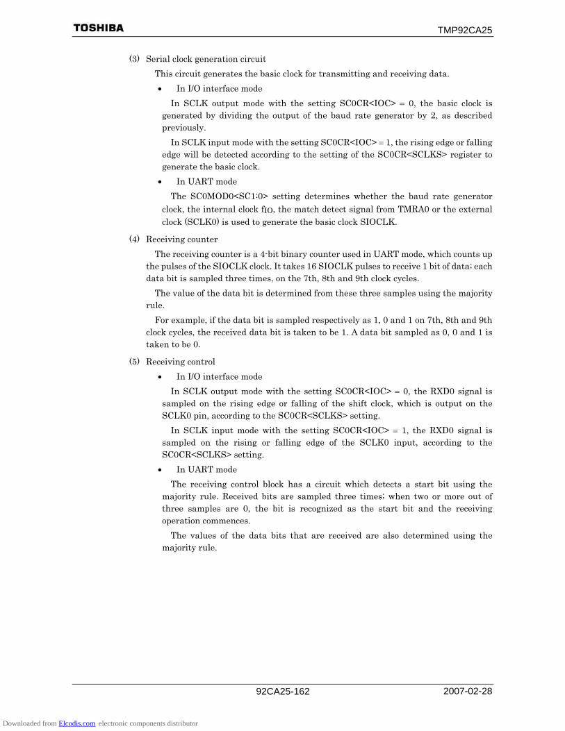
TMP92CA25
2007-02-28 92CA25-162
(3) Serial clock generation circuit This circuit generates the basic clock for transmitting and receiving data. • In I/O interface mode
In SCLK output mode with the setting SC0CR<IOC> = 0, the basic clock is generated by dividing the output of the baud rate generator by 2, as described previously.
In SCLK input mode with the setting SC0CR<IOC> = 1, the rising edge or falling edge will be detected according to the setting of the SC0CR<SCLKS> register to generate the basic clock.
• In UART mode The SC0MOD0<SC1:0> setting determines whether the baud rate generator
clock, the internal clock fIO, the match detect signal from TMRA0 or the external clock (SCLK0) is used to generate the basic clock SIOCLK.
(4) Receiving counter The receiving counter is a 4-bit binary counter used in UART mode, which counts up
the pulses of the SIOCLK clock. It takes 16 SIOCLK pulses to receive 1 bit of data; each data bit is sampled three times, on the 7th, 8th and 9th clock cycles.
The value of the data bit is determined from these three samples using the majority rule.
For example, if the data bit is sampled respectively as 1, 0 and 1 on 7th, 8th and 9th clock cycles, the received data bit is taken to be 1. A data bit sampled as 0, 0 and 1 is taken to be 0.
(5) Receiving control • In I/O interface mode
In SCLK output mode with the setting SC0CR<IOC> = 0, the RXD0 signal is sampled on the rising edge or falling of the shift clock, which is output on the SCLK0 pin, according to the SC0CR<SCLKS> setting.
In SCLK input mode with the setting SC0CR<IOC> = 1, the RXD0 signal is sampled on the rising or falling edge of the SCLK0 input, according to the SC0CR<SCLKS> setting.
• In UART mode The receiving control block has a circuit which detects a start bit using the
majority rule. Received bits are sampled three times; when two or more out of three samples are 0, the bit is recognized as the start bit and the receiving operation commences.
The values of the data bits that are received are also determined using the majority rule.
Downloaded from Elcodis.com electronic components distributor
TMP92CA25
2007-02-28 92CA25-163
(6) The receiving buffers To prevent overrun errors, the receiving buffers are arranged in a double buffer
structure. Received data is stored one bit at a time in receiving buffer 1 (which is a shift
register). When 7 or 8 bits of data have been stored in receiving buffer 1, the stored data is transferred to receiving buffer 2 (SC0BUF); this causes an INTRX0 interrupt to be generated. The CPU only reads receiving buffer 2 (SC0BUF). Even before the CPU reads receiving buffer 2 (SC0BUF), the received data can be stored in receiving buffer 1. However, unless receiving buffer 2 (SC0BUF) is read before all bits of the next data are received by receiving buffer 1, an overrun error occurs. If an overrun error occurs, the contents of receiving buffer 1 will be lost, although the contents of receiving buffer 2 and SC0CR<RB8> will be preserved.
SC0CR<RB8> is used to store either the parity bit – added in 8-bit UART mode – or the most significant bit (MSB) – in 9-bit UART mode.
In 9-bit UART mode the wakeup function for the slave controller is enabled by setting SC0MOD0<WU> to 1; in this mode INTRX0 interrupts occur only when the value of SC0CR<RB8> is 1.
SIO interrupt mode is selectable by the register SIMC.
(7) Transmission counter The transmission counter is a 4-bit binary counter used in UART mode and which,
like the receiving counter, counts the SIOCLK clock pulses; a TXDCLK pulse is generated every 16 SIOCLK clock pulses.
Figure 3.9.3 Generation of the Transmission Clock
(8) Transmission controller • In I/O interface mode
In SCLK output mode with the setting SC0CR<IOC> = 0, the data in the transmission buffer is output one bit at a time to the TXD0 pin on the rising or falling edge of the shift clock which is output on the SCLK0 pin, according to the SC0CR<SCLKS> setting.
In SCLK input mode with the setting SC0CR<IOC> = 1, the data in the transmission buffer is output one bit at a time on the TXD0 pin on the rising or falling edge of the SCLK0 input, according to the SC0CR<SCLKS> setting.
• In UART mode When transmission data sent from the CPU is written to the transmission buffer,
transmission starts on the rising edge of the next TXDCLK, generating a transmission shift clock TXDSFT.
15 16 1 2 3 4 5 6 7 8 9 10 11 12 13 14 15 16 1 2SIOCLK
TXDCLK
Downloaded from Elcodis.com electronic components distributor

TMP92CA25
2007-02-28 92CA25-164
Handshake function Use of CTS0 pin allows data to be sent in units of one frame; thus, overrun
errors can be avoided. The handshake function is enabled or disabled by the SC0MOD<CTSE> setting.
When the CTS0 pin goes high on completion of the current data send, data transmission is halted until the CTS0 pin goes low again. However, the INTTX0 interrupt is generated, and it requests the next data send from the CPU. The next data is written in the transmission buffer and data sending is halted.
Though there is no RTS pin, a handshake function can be easily configured by setting any port assigned to be the RTS function. The RTS should be output “high” to request send data halt after data receive is completed by software in the RXD interrupt routine.
Figure 3.9.4 Handshake Function
Note 1: If the CTS0 signal goes high during transmission, no more data will be sent after completion of the current
transmission. Note 2: Transmission starts on the first falling edge of the TXDCLK clock after the CTS0 signal has fallen.
Figure 3.9.5 CTS0 (Clear to send) Timing
TXD
CTS0
RXD RTS (Any port)
TMP92CA25 TMP92CA25
Sender Receiver
313 14 15 16 1 2
SIOCLK
314 15 16 1 2
Start bit bit0
(1) (2)Send is suspended from (1) and (2)
Timing of writing to thetransmission buffer
TXDCLK
TXD
CTS0
Downloaded from Elcodis.com electronic components distributor

TMP92CA25
2007-02-28 92CA25-165
(9) Transmission buffer The transmission buffer (SC0BUF) shifts out and sends the transmission data
written from the CPU in order from the least significant bit (LSB). When all the bits are shifted out, the transmission buffer becomes empty and generates an INTTX0 interrupt.
(10) Parity control circuit When SC0CR<PE> in the serial channel control register is set to “1”, it is possible to
transmit and receive data with parity. However, parity can be added only in 7-bit UART mode or 8-bit UART mode. The SC0CR<EVEN> field in the serial channel control register allows either even or odd parity to be selected.
In the case of transmission, parity is automatically generated when data is written to the transmission buffer SC0BUF. The data is transmitted after the parity bit has been stored in SC0BUF<TB7> in 7-bit UART mode or in SC0MOD0<TB8> in 8-bit UART mode. SC0CR<PE> and SC0CR<EVEN> must be set before the transmission data is written to the transmission buffer.
In the case of receiving, data is shifted into receiving buffer 1, and the parity is added after the data has been transferred to receiving buffer 2 (SC0BUF), and then compared with SC0BUF<RB7> in 7-bit UART mode or with SC0CR<RB8> in 8-bit UART mode. If they are not equal, a parity error is generated and the SC0CR<PERR> flag is set.
(11) Error flags Three error flags are provided to increase the reliability of data reception.
1. Overrun error <OERR> If all the bits of the next data item have been received in receiving buffer 1 while
valid data still remains stored in receiving buffer 2 (SC0BUF), an overrun error is generated.
The below is a recommended flow when the overrun-error is generated. (INTRX interrupt routine) 1) Read receiving buffer 2) Read error flag 3) If <OERR> = 1 then a) Set to disable receiving (Write “0” to SC0MOD0<RXE>) b) Wait to terminate current frame c) Read receiving buffer d) Read error flag e) Set to enable receiving (Write “1” to SC0MOD0<RXE>) f) Request to transmit again 4) Other
Downloaded from Elcodis.com electronic components distributor

TMP92CA25
2007-02-28 92CA25-166
2. Parity error <PERR> The parity generated for the data shifted into receiving buffer 2 (SC0BUF) is
compared with the parity bit received via the RXD pin. If they are not equal, a parity error is generated.
3. Framing error <FERR>
The stop bit for the received data is sampled three times around the center. If the majority of the samples are 0, a framing error is generated.
Downloaded from Elcodis.com electronic components distributor

TMP92CA25
2007-02-28 92CA25-167
(12) Timing generation 1. In UART mode
Receiving
Mode 9 Bits (Note) 8 Bits + Parity (Note) 8 Bits, 7 Bits + Parity,
7 Bits
Interrupt Timing Center of last bit (bit8)
Center of last bit (parity bit) Center of stop bit
Framing Error Timing Center of stop bit Center of stop bit Center of stop bit
Parity Error Timing − Center of last bit (parity bit) Center of stop bit
Overrun Error Timing Center of last bit (bit8)
Center of last bit (parity bit) Center of stop bit
Note1: In 9-bit and 8-bit + parity modes, interrupts coincide with the ninth bit pulse.
Thus, when servicing the interrupt, it is necessary to wait for a 1-bit period (to allow the stop bit to be
transferred) to allow checking for a framing error.
Note2: The higher the transfer rate, the later than the middle receive interrupts and errors occur.
Transmitting
Mode 9 Bits 8 Bits + Parity 8 Bits, 7 Bits + Parity, 7 Bits
Interrupt Timing Just before stop bit is transmitted
Just before stop bit is transmitted
Just before stop bit is transmitted
2. I/O interface
SCLK output mode Immediately after last bit data. (See Figure 3.9.13.) Transmission
Interrupt Timing SCLK input mode Immediately after rise of last SCLK signal rising mode, or
immediately after fall in falling mode. (See Figure 3.9.14.)
SCLK output mode Timing used to transfer received to data receive buffer 2 (SC0BUF) (e.g. immediately after last SCLK). (See Figure 3.9.15.) Receiving
Interrupt Timing SCLK input mode Timing used to transfer received data to receive buffer 2 (SC0BUF)
(e.g. immediately after last SCLK). (See Figure 3.9.16.)
Downloaded from Elcodis.com electronic components distributor
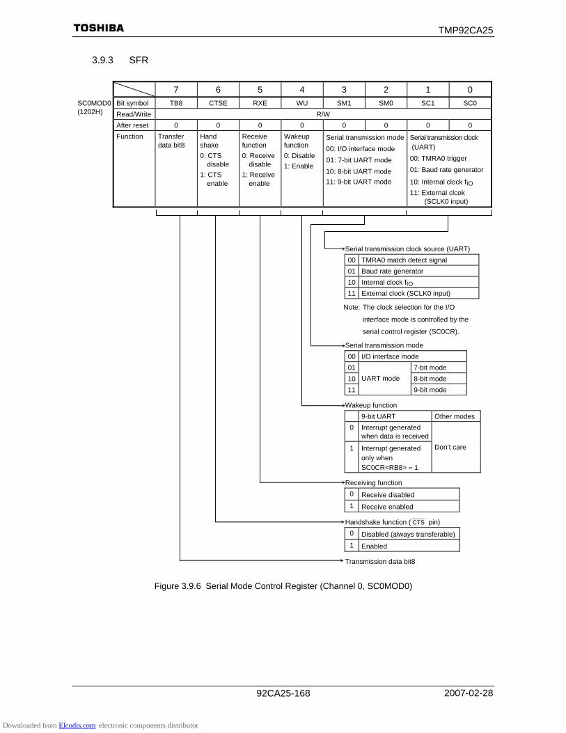
TMP92CA25
2007-02-28 92CA25-168
3.9.3 SFR
7 6 5 4 3 2 1 0
Bit symbol TB8 CTSE RXE WU SM1 SM0 SC1 SC0 SC0MOD0 (1202H) Read/Write R/W After reset 0 0 0 0 0 0 0 0 Function Transfer
data bit8 Hand shake 0: CTS
disable 1: CTS
enable
Receive function 0: Receive
disable 1: Receive
enable
Wakeup function 0: Disable 1: Enable
Serial transmission mode 00: I/O interface mode 01: 7-bit UART mode 10: 8-bit UART mode 11: 9-bit UART mode
Serial transmission clock (UART) 00: TMRA0 trigger 01: Baud rate generator
10: Internal clock fIO 11: External clcok
(SCLK0 input)
Serial transmission clock source (UART) 00 TMRA0 match detect signal 01 Baud rate generator 10 Internal clock fIO 11 External clock (SCLK0 input)
Note: The clock selection for the I/O
interface mode is controlled by the
serial control register (SC0CR).
Serial transmission mode 00 I/O interface mode 01 7-bit mode 10 8-bit mode 11
UART mode 9-bit mode
Wakeup function 9-bit UART Other modes
0 Interrupt generated when data is received
1 Interrupt generated only when SC0CR<RB8> = 1
Don’t care
Receiving function 0 Receive disabled 1 Receive enabled
Handshake function ( CTS pin) 0 Disabled (always transferable) 1 Enabled
Transmission data bit8
Figure 3.9.6 Serial Mode Control Register (Channel 0, SC0MOD0)
Downloaded from Elcodis.com electronic components distributor

TMP92CA25
2007-02-28 92CA25-169
7 6 5 4 3 2 1 0
Bit symbol RB8 EVEN PE OERR PERR FERR SCLKS IOC SC0CR (1201H) Read/Write R R/W R (Cleared to 0 when read) R/W After reset Undefined 0 0 0 0 0 0 0
1: Error Function Received
data bit8 Parity 0: Odd 1: Even
Parity addition 0: Disable 1: Enable
Overrun Parity Framing
0: SCLK0 1: SCLK0
0: Baud rate generator
1: SCLK0 pin input
I/O interface input clock selection 0 Baud rate generator 1 SCLK0 pin input
Edge selection for SCLK pin (I/O mode) 0 Transmits and receives
data on rising edge of SCLK0. 1 Transmits and receives
data on falling edge SCLK0. Framing error flag Parity error flag Overrun error flag
Cleared to 0 when read
Parity additions enable 0 Disabled 1 Enabled
Even parity addition/check 0 Odd parity 1 Even parity
Received data bit8
Note: As all error flags are cleared after reading do not test only a single bit with a bit testing instruction.
Figure 3.9.7 Serial Control Register (Channel 0, SC0CR)
Downloaded from Elcodis.com electronic components distributor

TMP92CA25
2007-02-28 92CA25-170
7 6 5 4 3 2 1 0
Bit symbol − BR0ADDE BR0CK1 BR0CK0 BR0S3 BR0S2 BR0S1 BR0S0 BR0CR (1203H) Read/Write R/W After reset 0 0 0 0 0 0 0 0 Function Always
write “0”. +(16 − K)/16 division 0: Disable 1: Enable
00: φT0 01: φT2 10: φT8 11: φT32
Divided frequency setting
7 6 5 4 3 2 1 0 Bit symbol BR0K3 BR0K2 BR0K1 BR0K0 BR0ADD
(1204H) Read/Write R/W After reset 0 0 0 0 Function
Sets frequency divisor “K” (divided by N + (16 − K)/16).
Sets baud rate generator frequency divisor BR0CR<BR0ADDE> = 1 BR0CR<BR0ADDE> = 0
BR0CR <BR0S3:0>
BR0ADD <BR0K3:0>
0000 (N = 16) or
0001 (N = 1)
0010 (N = 2)to
1111 (N = 15)
0001 (N = 1) (Only UART)to
1111 (N = 15) 0000 (N = 16)
0000 Disable Disable 0001 (K = 1)
to 1111 (K = 15)
Disable Divided by N + (16 − K)/16
Divided by N
Note1:Availability of +(16-K)/16 division function
N UART mode I/O mode
2 to 15 ○ ×
1 , 16 × ×
The baud rate generator can be set to “1” in UART mode only when the +(16-K)/16 division function is not used. Do not
use in I/O interface mode.
Note2:Set BR0CR <BR0ADDE> to 1 after setting K (K = 1 to 15) to BR0ADD<BR0K3:0> when +(16-K)/16 division function is
used. Writes to unused bits in the BR0ADD register do not affect operation, and undefined data is read from these
unused bits.
Figure 3.9.8 Baud Rate Generator Control (Channel 0, BR0CR, BR0ADD)
Setting the input clock of baud rate generator 00 Internal clock φT0 01 Internal clock φT2 10 Internal clock φT8 11 Internal clock φT32
+(16 − K)/16 division enable 0 Disable 1 Enable
Downloaded from Elcodis.com electronic components distributor
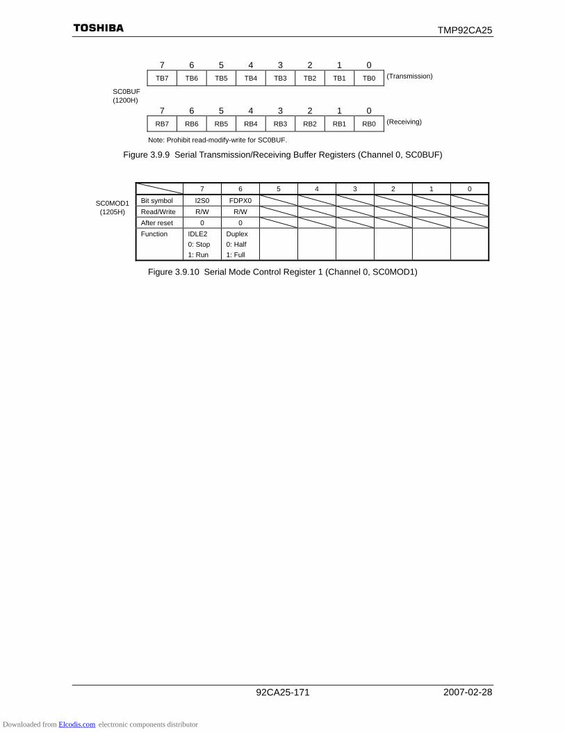
TMP92CA25
2007-02-28 92CA25-171
7 6 5 4 3 2 1 0 TB7 TB6 TB5 TB4 TB3 TB2 TB1 TB0 (Transmission)
SC0BUF (1200H)
7 6 5 4 3 2 1 0 RB7 RB6 RB5 RB4 RB3 RB2 RB1 RB0 (Receiving)
Note: Prohibit read-modify-write for SC0BUF.
Figure 3.9.9 Serial Transmission/Receiving Buffer Registers (Channel 0, SC0BUF)
7 6 5 4 3 2 1 0
Bit symbol I2S0 FDPX0 Read/Write R/W R/W After reset 0 0 Function IDLE2
0: Stop 1: Run
Duplex 0: Half 1: Full
Figure 3.9.10 Serial Mode Control Register 1 (Channel 0, SC0MOD1)
SC0MOD1 (1205H)
Downloaded from Elcodis.com electronic components distributor

TMP92CA25
2007-02-28 92CA25-172
3.9.4 Operation in Each Mode
(1) Mode 0 (I/O interface mode) This mode allows an increase in the number of I/O pins available for transmitting
data to or receiving data from an external shift register. This mode includes the SCLK output mode to output synchronous clock SCLK, and
SCLK input mode to input external synchronous clock SCLK.
Figure 3.9.11 SCLK Output Mode Connection Example
Figure 3.9.12 Example of SCLK Input Mode Connection
Output extension
TC74HC595 or equivalent
AB
SI CD
SCK EF
RCK GH
TXD
SCLK
Port
Shift register TMP92CA25
Input extension
TC74HC165 or equivalent
A B
QH C D
CLOCK E F
S/ L G H
RXD
SCLK
Port
Shift register TMP92CA25
Output extension
TC74HC595 or equivalent
AB
SI CD
SCK EF
RCK GH
TXD
SCLK
Port
Shift register TMP92CA25
Input extension
TC74HC165 or equivalent
A B
QH C D
CLOCK E F
S/ L G H
RXD
SCLK
Port
Shift register TMP92CA25
External clock External clock
Downloaded from Elcodis.com electronic components distributor
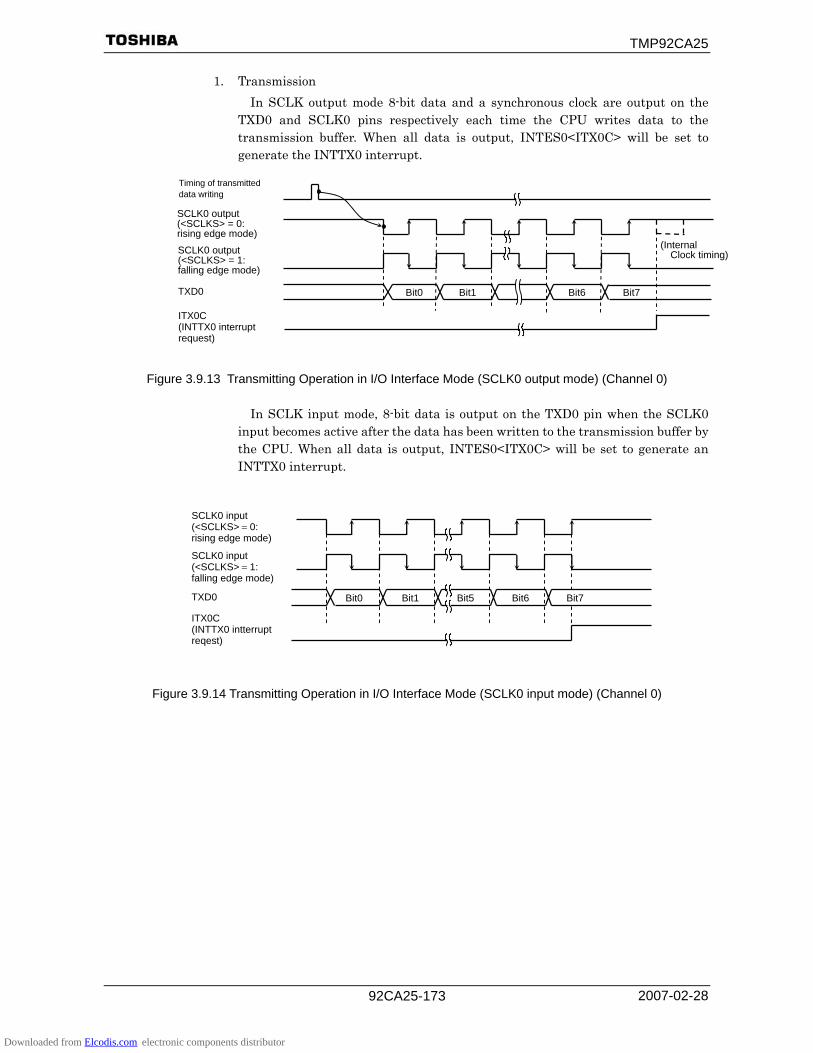
TMP92CA25
2007-02-28 92CA25-173
1. Transmission In SCLK output mode 8-bit data and a synchronous clock are output on the
TXD0 and SCLK0 pins respectively each time the CPU writes data to the transmission buffer. When all data is output, INTES0<ITX0C> will be set to generate the INTTX0 interrupt.
Figure 3.9.13 Transmitting Operation in I/O Interface Mode (SCLK0 output mode) (Channel 0)
In SCLK input mode, 8-bit data is output on the TXD0 pin when the SCLK0 input becomes active after the data has been written to the transmission buffer by the CPU. When all data is output, INTES0<ITX0C> will be set to generate an INTTX0 interrupt.
Figure 3.9.14 Transmitting Operation in I/O Interface Mode (SCLK0 input mode) (Channel 0)
Bit0 Bit1 Bit6 Bit7 Bit5
SCLK0 input (<SCLKS> = 0: rising edge mode)
SCLK0 input (<SCLKS> = 1: falling edge mode)
TXD0
ITX0C (INTTX0 intterrupt reqest)
TXD0
ITX0C (INTTX0 interrupt request)
SCLK0 output (<SCLKS> = 0: rising edge mode)
Timing of transmitted data writing
Bit0 Bit1 Bit6 Bit7
SCLK0 output (<SCLKS> = 1: falling edge mode)
(Internal Clock timing)
Downloaded from Elcodis.com electronic components distributor

TMP92CA25
2007-02-28 92CA25-174
2. Receiving In SCLK output mode the synchronous clock is output on the SCLK0 pin and
the data is shifted to receiving buffer 1. This is initiated when the receive interrupt flag INTES0<IRX0C> is cleared as the received data is read. When 8-bit data is received, the data is transferred to receiving buffer 2 (SC0BUF) following the timing shown below and INTES0<IRX0C> is set to 1 again, causing an INTRX0 interrupt to be generated.
Setting SC0MOD0<RXE> to 1 initiates SCLK0 output.
Figure 3.9.15 Receiving Operation in I/O Interface Mode (SCLK0 output mode)
In SCLK input mode the data is shifted to receiving buffer 1 when the SCLK input goes active. The SCLK input goes active when the receive interrupt flag INTES0<IRX0C> is cleared as the received data is read. When 8-bit data is received, the data is shifted to receiving buffer 2 (SC0BUF) following the timing shown below and INTES0<IRX0C> is set to 1 again, causing an INTRX0 interrupt to be generated.
Figure 3.9.16 Receiving Operation in I/O Interface Mode (SCLK0 input mode)
Note: The system must be put in the receive-enable state (SC0MOD0<RXE> = 1) before data can be received.
SCLK0 output(<SCLKS> = 0: rising edge mode)
IRX0C (INTRX0 interrupt request)
RXD0 Bit0 Bit1 Bit6 Bit7
SCLK0 output(<SCLKS> = 1: falling edge mode)
SCLK0 input (<SCLKS> = 0: rising edge mode)
SCLK0 input (<SCLKS> = 1: falling edge mode)
IRX0C (INTRX0 interrupt request)
RXD1 Bit1 Bit6 Bit7 Bit5 Bit0
Downloaded from Elcodis.com electronic components distributor
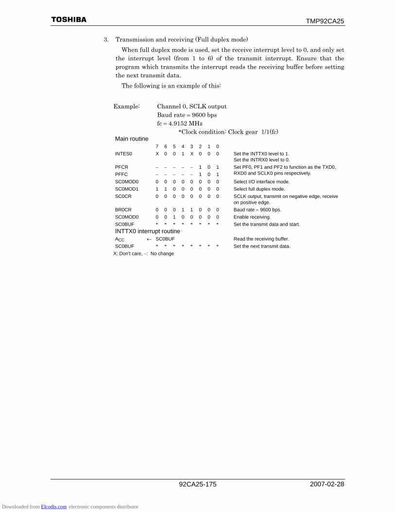
TMP92CA25
2007-02-28 92CA25-175
3. Transmission and receiving (Full duplex mode) When full duplex mode is used, set the receive interrupt level to 0, and only set
the interrupt level (from 1 to 6) of the transmit interrupt. Ensure that the program which transmits the interrupt reads the receiving buffer before setting the next transmit data.
The following is an example of this:
Example: Channel 0, SCLK output Baud rate = 9600 bps fc = 4.9152 MHz
*Clock condition: Clock gear 1/1(fc) Main routine 7 6 5 4 3 2 1 0 INTES0 X 0 0 1 X 0 0 0 Set the INTTX0 level to 1.
Set the INTRX0 level to 0. PFCR − − − − − 1 0 1PFFC − − − − − 1 0 1
Set PF0, PF1 and PF2 to function as the TXD0, RXD0 and SCLK0 pins respectively.
SC0MOD0 0 0 0 0 0 0 0 0 Select I/O interface mode. SC0MOD1 1 1 0 0 0 0 0 0 Select full duplex mode. SC0CR 0 0 0 0 0 0 0 0 SCLK output, transmit on negative edge, receive
on positive edge. BR0CR 0 0 0 1 1 0 0 0 Baud rate = 9600 bps. SC0MOD0 0 0 1 0 0 0 0 0 Enable receiving. SC0BUF * * * * * * * * Set the transmit data and start. INTTX0 interrupt routine ACC ← SC0BUF Read the receiving buffer. SC0BUF * * * * * * * * Set the next transmit data.
X: Don't care, −: No change
Downloaded from Elcodis.com electronic components distributor
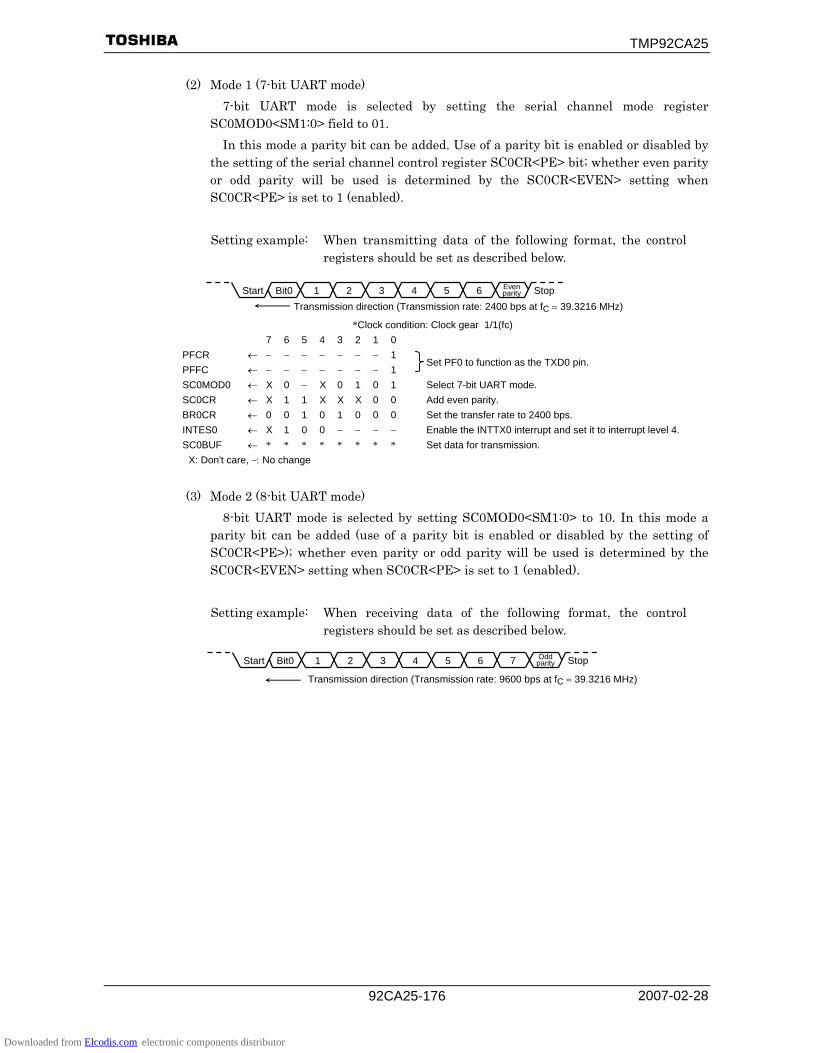
TMP92CA25
2007-02-28 92CA25-176
(2) Mode 1 (7-bit UART mode) 7-bit UART mode is selected by setting the serial channel mode register
SC0MOD0<SM1:0> field to 01. In this mode a parity bit can be added. Use of a parity bit is enabled or disabled by
the setting of the serial channel control register SC0CR<PE> bit; whether even parity or odd parity will be used is determined by the SC0CR<EVEN> setting when SC0CR<PE> is set to 1 (enabled).
Setting example: When transmitting data of the following format, the control
registers should be set as described below.
*Clock condition: Clock gear 1/1(fc) 7 6 5 4 3 2 1 0 PFCR ← − − − − − − − 1PFFC ← − − − − − − − 1
Set PF0 to function as the TXD0 pin.
SC0MOD0 ← X 0 − X 0 1 0 1 Select 7-bit UART mode. SC0CR ← X 1 1 X X X 0 0 Add even parity. BR0CR ← 0 0 1 0 1 0 0 0 Set the transfer rate to 2400 bps. INTES0 ← X 1 0 0 − − − − Enable the INTTX0 interrupt and set it to interrupt level 4.SC0BUF ← * * * * * * * * Set data for transmission.
X: Don't care, −: No change
(3) Mode 2 (8-bit UART mode) 8-bit UART mode is selected by setting SC0MOD0<SM1:0> to 10. In this mode a
parity bit can be added (use of a parity bit is enabled or disabled by the setting of SC0CR<PE>); whether even parity or odd parity will be used is determined by the SC0CR<EVEN> setting when SC0CR<PE> is set to 1 (enabled).
Setting example: When receiving data of the following format, the control
registers should be set as described below.
Transmission direction (Transmission rate: 9600 bps at fC = 39.3216 MHz)
Start Bit0 1 2 3 4 5 6 Oddparity Stop 7
Start Bit0 1 2 3 4 5 6 Evenparity Stop
Transmission direction (Transmission rate: 2400 bps at fC = 39.3216 MHz)
Downloaded from Elcodis.com electronic components distributor

TMP92CA25
2007-02-28 92CA25-177
Main settings 7 6 5 4 3 2 1 0 PFCR ← − − − − − − 0 − Set PF1 to function as the RXD0 pin. PFFC ← − − − − − − 0 − SC0MOD0 ← − 0 1 X 1 0 0 1 Enable receiving in 8-bit UART mode. SC0CR ← X 0 1 X X X 0 0 Add odd parity. BR0CR ← 0 0 0 1 1 0 0 0 Set the transfer rate to 9600 bps. INTES0 ← − − − − X 1 0 0 Enable the INTTX0 interrupt and set it to interrupt
level 4. Interrupt processing ACC ← SC0CR AND 00011100 if ACC ≠ 0 then ERROR
Check for errors
ACC ← SC0BUF Read the received data X: Don't care, −: No change
(4) Mode 3 (9-bit UART mode) 9-bit UART mode is selected by setting SC0MOD0<SM1:0> to 11. In this mode a
parity bit cannot be added. In the case of transmission the MSB (9th bit) is written to SC0MOD0<TB8>. In the
case of receiving it is stored in SC0CR<RB8>. When the buffer is written or read, <TB8>or <RB8> is read or written first, before the rest of the SC0BUF data.
Wakeup function In 9-bit UART mode, the wakeup function for slave controllers is enabled by
setting SC0MOD0<WU> to 1. The interrupt INTRX0 can only be generated when<RB8> = 1.
Note: The TXD pin of each slave controller must be in open-drain output mode.
Figure 3.9.17 Serial Link Using Wakeup Function
TXD RXD
Master
TXD RXD
Slave1
TXD RXD
Slave 2
TXD RXD
Slave 3
Downloaded from Elcodis.com electronic components distributor

TMP92CA25
2007-02-28 92CA25-178
Protocol
1. Select 9-bit UART mode on the master and slave controllers.
2. Set the SC0MOD0<WU> bit on each slave controller to 1 to enable data receiving.
3. The master controller transmits data one frame at a time. Each frame includes an 8-bit select code which identifies a slave controller. The MSB (bit8) of the data (<TB8>) is set to 1.
4. Each slave controller receives the above frame. Each controller checks the above select code against its own select code. The controller whose code matches clears its <WU> bit to 0.
5. The master controller transmits data to the specified slave controller (the controller whose SC0MOD0<WU> bit has been cleared to 0). The MSB (bit8) of the data (<TB8>) is cleared to 0.
6. The other slave controllers (whose <WU> bits remain at 1) ignore the received data because their MSBs (bit8 or <RB8>) are set to 0, disabling INTRX0 interrupts. The slave controller whose <WU> bit = 0 can also transmit to the master controller. In this way it can signal the master controller that the data transmission from the master controller has been completed.
Start Bit0 1 2 3 4 5 6
Select code of slave controller
7 Stop8
“1”
Data “0”
Start Bit0 1 2 3 4 5 6 7 StopBit8
Downloaded from Elcodis.com electronic components distributor

TMP92CA25
2007-02-28 92CA25-179
Setting example: To link two slave controllers serially with the master controller using the internal clock fIO as the transfer clock.
• Setting the master controller Main PFCR ← − − − − − − 0 1PFFC ← − − − − − − 0 1
Set PF0 and PF1 to function as the TXD0 and RXD0 pins respectively.
INTES0 ← 1 1 0 0 1 1 0 1 Enable the INTTX0 interrupt and set it to interrupt level 4. Enable the INTRX0 interrupt and set it to interrupt level 5.
SC0MOD0 ← 1 0 1 0 1 1 1 0 Set fIO as the transmission clock for 9-bit UART mode. SC0BUF ← 0 0 0 0 0 0 0 1 Set the select code for slave controller 1. INTTX0 interrupt SC0MOD0 ← 0 − − − − − − − Set TB8 to 0. SC0BUF ← * * * * * * * * Set data for transmission.
• Setting the slave controller
Main PFCR ← − − − − − − 0 1PFFC ← − − − − − − 0 1PFFC2 ← X X X X X X X 1
Select PF1 and PF0 to function as the RXD0 and TXD0 pins respectively (Open-drain output).
INTES0 ← 1 1 0 1 1 1 1 0 Enable INTRX0 and INTTX0. SC0MOD0 ← 1 0 1 1 1 1 1 0 Set <WU> to 1 in 9-bit UART transmission mode using fSYS as
the transfer clock. INTRX0 interrupt ACC ← SC0BUF if ACC = select code Then SC0MOD0 ← − − − 0 − − − − Clear <WU> to 0
TXD RXD
Master
TXD RXD
Slave1
TXD RXD
Slave 2
Select code00000001
Select code 00001010
Downloaded from Elcodis.com electronic components distributor
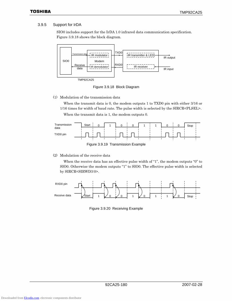
TMP92CA25
2007-02-28 92CA25-180
3.9.5 Support for IrDA
SIO0 includes support for the IrDA 1.0 infrared data communication specification. Figure 3.9.18 shows the block diagram.
Figure 3.9.18 Block Diagram
(1) Modulation of the transmission data When the transmit data is 0, the modem outputs 1 to TXD0 pin with either 3/16 or
1/16 times for width of baud rate. The pulse width is selected by the SIRCR<PLSEL>. When the transmit data is 1, the modem outputs 0.
Figure 3.9.19 Transmission Example
(2) Modulation of the receive data When the receive data has an effective pulse width of “1”, the modem outputs “0” to
SIO0. Otherwise the modem outputs “1” to SIO0. The effective pulse width is selected by SIRCR<SIRWD3:0>.
Figure 3.9.20 Receiving Example
Start Transmission data
Stop0 0 0010 11
TXD0 pin
Start Receive data Stop1 1001 01 0
RXD0 pin
Transmission data
SIO0
IR modulator
IR demodulatorReceive data
IR transmitter & LED
IR receiver
Modem
TXD0
RXD0
IR output
IR input
TMP92CA25
Downloaded from Elcodis.com electronic components distributor
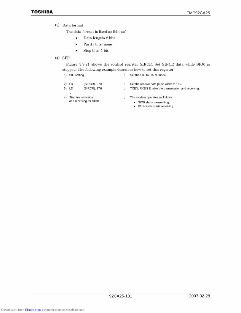
TMP92CA25
2007-02-28 92CA25-181
(3) Data format The data format is fixed as follows:
• Data length: 8 bits • Parity bits: none • Stop bits: 1 bit
(4) SFR Figure 3.9.21 shows the control register SIRCR. Set SIRCR data while SIO0 is
stopped. The following example describes how to set this register: 1) SIO setting ; Set the SIO to UART mode. ↓ 2) LD (SIRCR), 07H ; Set the receive data pulse width to 16×. 3) LD (SIRCR), 37H ; TXEN, RXEN Enable the transmission and receiving. ↓ 4) Start transmission
and receiving for SIO0 ; The modem operates as follows:
• SIO0 starts transmitting. • IR receiver starts receiving.
Downloaded from Elcodis.com electronic components distributor

TMP92CA25
2007-02-28 92CA25-182
(5) Notes 1. Baud rate for IrDA
When IrDA is operated, set 01 to SC0MOD0<SC1:0> to generate baud rate. Settings other than the above (TA0TRG, fIO and SCLK0 input) cannot be used.
2. The pulse width for transmission The IrDA 1.0 specification is defined in Table 3.9.3.
Table 3.9.3 Baud Rate and Pulse Width Specifications
Baud Rate Modulation Rate Tolerance
(% of rate) Pulse Width
(min) Pulse Width
(typ.) Pulse Width
(max)
2.4 Kbps RZI ±0.87 1.41 μs 78.13 μs 88.55 μs 9.6 Kbps RZI ±0.87 1.41 μs 19.53 μs 22.13 μs
19.2 Kbps RZI ±0.87 1.41 μs 9.77 μs 11.07 μs 38.4 Kbps RZI ±0.87 1.41 μs 4.88 μs 5.96 μs 57.6 Kbps RZI ±0.87 1.41 μs 3.26 μs 4.34 μs
115.2 Kbps RZI ±0.87 1.41 μs 1.63 μs 2.23 μs
The pulse width is defined as either baud rate T × 3/16 or 1.6 μs (1.6 μs is equal
to 3/16 pulse width when baud rate is 115.2 Kbps). The TMP92CA25 has a function which can select the pulse width of
transmission as either 3/16 or 1/16. However, 1/16 pulse width can only be selected when the baud rate is equal to or less than 38.4 Kbps.
For the same reason, when using IrDA 115.2 Kbps with USB, the + (16 − K)/16 division function in the baud rate generator of SIO0 cannot be used to generate a 115.2 Kbps baud rate, except under special conditions as explained in (6) below.
The + (16 − K)/16 division function cannot be used alsowhen the baud rate is 38.4 Kbps and the pulse width is 1/16.
Table 3.9.4 Baud Rate and Pulse Width for (16 − K)/16 Division Function
Baud Rate Pulse Width
115.2 Kbps 57.6 Kbps 38.4 Kbps 19.2 Kbps 9.6 Kbps 2.4 Kbps T × 3/16 × (Note) ○ ○ ○ ○ ○ T × 1/16 − − × ○ ○ ○
○: (16 − K)/16 division function can be used. ×: (16 − K)/16 division function cannot be used. −: Cannot be set to 1/16 pulse width.
Note: (16 − K)/16 division function can be used under special
conditions.
Downloaded from Elcodis.com electronic components distributor

TMP92CA25
2007-02-28 92CA25-183
7 6 5 4 3 2 1 0
Bit symbol PLSEL RXSEL TXEN RXEN SIRWD3 SIRWD2 SIRWD1 SIRWD0SIRCR (1207H) Read/Write R/W After reset 0 0 0 0 0 0 0 0 Function Select
transmit pulse width 0: 3/16 1: 1/16
Receive data 0: “H” pulse 1: “L” pulse
Transmit 0: Disable 1: Enable
Receive 0: Disable 1: Enable
Select receive pulse width Set effective pulse width to equal to or more than 2x × (value + 1) + 100 ns Can be set: 1 to 14 Cannot be set: 0, 15
Select receive pulse width Formula: Effective pulse width ≥ 2x × (value + 1) + 100 ns x = 1/fSYS
0000 Cannot be set 0001 Equal to or more than 4x + 100 ns
to 1110 Equal to or more than 30x + 100 ns 1111 Cannot be set
Receive operation 0 Disable (Received input is ignored) 1 Enable
Transmit operation 0 Disable (Input from SIO is ignored) 1 Enable
Select transmit pulse width 0 3/16 1 1/16
Figure 3.9.21 IrDA Control Register
Note: If a pulse width complying with IrDA1.0 standard (1.6
μs min.) can be guaranteed with a low baud rate,
setting this bit to “1” will result in reduced power
dissipation.
Downloaded from Elcodis.com electronic components distributor

TMP92CA25
2007-02-28 92CA25-184
3.10 Serial Bus Interface (SBI)
The TMP92CA25 has 1-channel serial bus interface which an I2C bus mode. The serial bus interface is connected to an external device through P93 (SDA) and P94 (SCL)
in the I2C bus mode. Each pin is specified as follows.
P9F2<P94F2, P93F2> P9CR<P94C, P93C> P9FC<P94F, P93F >
I2C Bus Mode 11 11 11
X: Don’t care
3.10.1 Configuration
Figure 3.10.1 Serial Bus Interface (SBI)
SIO clock
control
Divider
I2C busclock
sync. + control
SBI0CR2/SBI0SR
SCL SCK
Input/ output control SO SI SDA
I2C0AR SBI0BR SBI0CR1 SBI0BR0, 1
Shift register
Transfer control circuit
Noise canceller
φT
Noise canceller
I2C bus data control
SIO data control
INTSBI interrupt request
P94 (SO/SDA)
P93 (SCL)
SBI0 control register 2/
SBI0 status register
I2C bus address register
SBI databuffer
register
SBI controlregister 1
SBI baud rate register 0, 1
Downloaded from Elcodis.com electronic components distributor

TMP92CA25
2007-02-28 92CA25-185
3.10.2 Serial Bus Interface (SBI) Control
The following registers are used to control the serial bus interface and monitor the operation status. • Serial bus interface 0 control register 1 (SBI0CR1)
• Serial bus interface 0 control register 2 (SBI0CR2)
• Serial bus interface 0 data buffer register (SBI0DBR)
• I2C bus 0 address register (I2C0AR)
• Serial bus interface 0 status register (SBI0SR)
• Serial bus interface 0 baud rate register 0 (SBI0BR0)
• Serial bus interface 0 baud rate register 1 (SBI0BR1) The above registers differ depending on a mode to be used. Refer to section 3.10.4 “I2C
Bus Mode Control Register”.
3.10.3 The Data Formats in the I2C Bus Mode
The data formats in the I2C bus mode is shown below.
(a) Addressing format
(b) Addressing format (with restart)
(c) Free data format (data transferred from master device to slave device)
Figure 3.10.2 Data Format in the I2C Bus Mode
S Slave address R /
W Data
A C K
ACK
S Slave address R/
WData
A C K
ACK
P
8 bits 1 1 to 8 bits 1 8 bits 1 1 to 8 bits 1
1 1 or more 1 1 or more
S Slave address R /
W Data
A C K
ACK
Data ACK
P
8 bits 1 1 to 8 bits 1 1 to 8 bits 1
1 1 or more
S Data Data A C K
ACK
Data ACK
P
8 bits 1 1 to 8 bits 1 1 to 8 bits 1
1 1 or more
S: Start condition
R/ W : Direction bit
ACK: Acknowledge bit
P: Stop condition
Downloaded from Elcodis.com electronic components distributor

TMP92CA25
2007-02-28 92CA25-186
3.10.4 I2C Bus Mode Control Register
The following registers are used to control and monitor the operation status when using the serial bus interface (SBI) in the I2C bus mode.
Serial Bus Interface 0 Control Register 1
7 6 5 4 3 2 1 0 Bit symbol BC2 BC1 BC0 ACK SCK2 SCK1 SCK0/
SWRMONRead/Write W R/W W R/W After reset 0 0 0 0 0 0 0/1 (Note 2)Function Number of transferred bits
Acknowl- edge mode specifica- tion
0: Not generate
1: Generate
Internal serial clock selection and software reset monitor (Note 1)
Internal serial clock selection <SCK2:0> at write 000001010011100101110111
n = 5n = 6n = 7n = 8n = 9n = 10n = 11
Reserved
− (Note 3)− (Note 3)− (Note 3)
− (Note 3)76.9 kHz 38.8 kHz 19.5 kHz (Reserved)
System clock: fSYS fSYS = 20 MHz (internal SCL output) fscl = [Hz]
Software reset state monitor <SWRMON> at read 0 During software reset 1 Initial data
Acknowledge mode specification 0 Not generate clock pulse for acknowledge signal 1 Generate clock pulse for acknowledge signal
Number of bits transferred <ACK> = 0 <ACK> = 1
<BC2:0> Number of clock pulses Bits
Number of clock
pulses Bits
000 001 010 011 100 101 110 111
8 1 2 3 4 5 6 7
8 1 2 3 4 5 6 7
9 2 3 4 5 6 7 8
8 1 2 3 4 5 6 7
Note 1: For the frequency of the SCL pin clock, see 3.10.5 (3) “Serial clock”.
Note 2: Initial data of SCK0 is “0”, SWRMON is “1”.
Note 3: This I2C bus circuit does not support fast mode, it supports the Standard mode only. Although the I2C bus
circuit itself allows the setting of a baud rate over 100kbps, the compliance with the I2C specification is not
guaranteed in that case.
Figure 3.10.3 Registers for the I2C Bus Mode
fSYS 2n + 8
SBI0CR1 (1240H) Prohibit read- modify- write
Downloaded from Elcodis.com electronic components distributor

TMP92CA25
2007-02-28 92CA25-187
Serial Bus Interface Control Register 2
7 6 5 4 3 2 1 0 Bit symbol MST TRX BB PIN SBIM1 SBIM0 SWRST1 SWRST0
Read/Write W W (Note 1) W (Note 1) After reset 0 0 0 1 0 0 0 0 Function Master/
slave selection
Transmitter/receiver selection
Start/stop condition generation
Cancel INTSBI interrupt request
Serial bus interface operating mode selection (Note 2) 00: Port mode 01: (Reserved) 10: I2C bus mode 11: (Reserved)
Software reset generate write “10” and “01”, then an internal software reset signal is generated.
Serial bus interface operating mode selection (Note 2) 00 Port mode (Serial bus interface output disabled) 01 (Reserved) 10 I2C bus mode 11 (Reserved)
INTSBI interrupt request 0 − (Cannot clear to “0”) 1 Cancel interrupt request
Start/stop condition generation 0 Generates the stop condition
(When MST, TRX, PIN are “1”) 1 Generates the start condition
(When MST, TRX, PIN are “1”)
Transmitter/receiver selection 0 Receiver 1 Transmitter
Master/slave selection 0 Slave 1 Master
Note 1: Reading this register function as SBI0SR register.
Note 2: Switch a mode to port mode after confirming that the bus is free.
Switch a mode between I2C bus mode after confirming that input signals via port are high level.
Figure 3.10.4 Registers for the I2C Bus Mode
SBI0CR2 (1243H) Prohibit read- modify- write
Downloaded from Elcodis.com electronic components distributor

TMP92CA25
2007-02-28 92CA25-188
Serial Bus Interface Status Register
7 6 5 4 3 2 1 0 Bit symbol MST TRX BB PIN AL AAS AD0 LRB
Read/Write R After reset 0 0 0 1 0 0 0 0 Function Master/
slave status monitor
Transmitter/ receiver status monitor
I2C bus status monitor
INTSBI interrupt request monitor
Arbitration lost detection monitor 0: − 1: Detected
Slave address match detection monitor 0: Undetected
1: Detected
GENERAL CALL detection monitor 0: Undetected
1: Detected
Last received bit monitor 0: “0” 1: “1”
Last received bit monitor 0 Last received bit was “0” 1 Last received bit was “1”
GENERAL CALL detection monitor 0 Undetected 1 GENERAL CALL detected
Slave address match detection monitor 0 Undetected
1 Slave address match or GENERAL CALL detected
Arbitration lost detection monitor 0 − 1 Arbitration lost
INTSBI interrupt request monitor 0 Interrupt requested 1 Interrupt canceled
I2C bus status monitor 0 Free 1 Busy
Transmitter/receiver status monitor 0 Receiver 1 Transmitter
Master/slave status monitor 0 Slave 1 Master
Note: Writing in this register functions as SBI0CR2.
Figure 3.10.5 Registers for the I2C Bus Mode
SBI0SR (1243H) Prohibit read- modify- write
Downloaded from Elcodis.com electronic components distributor
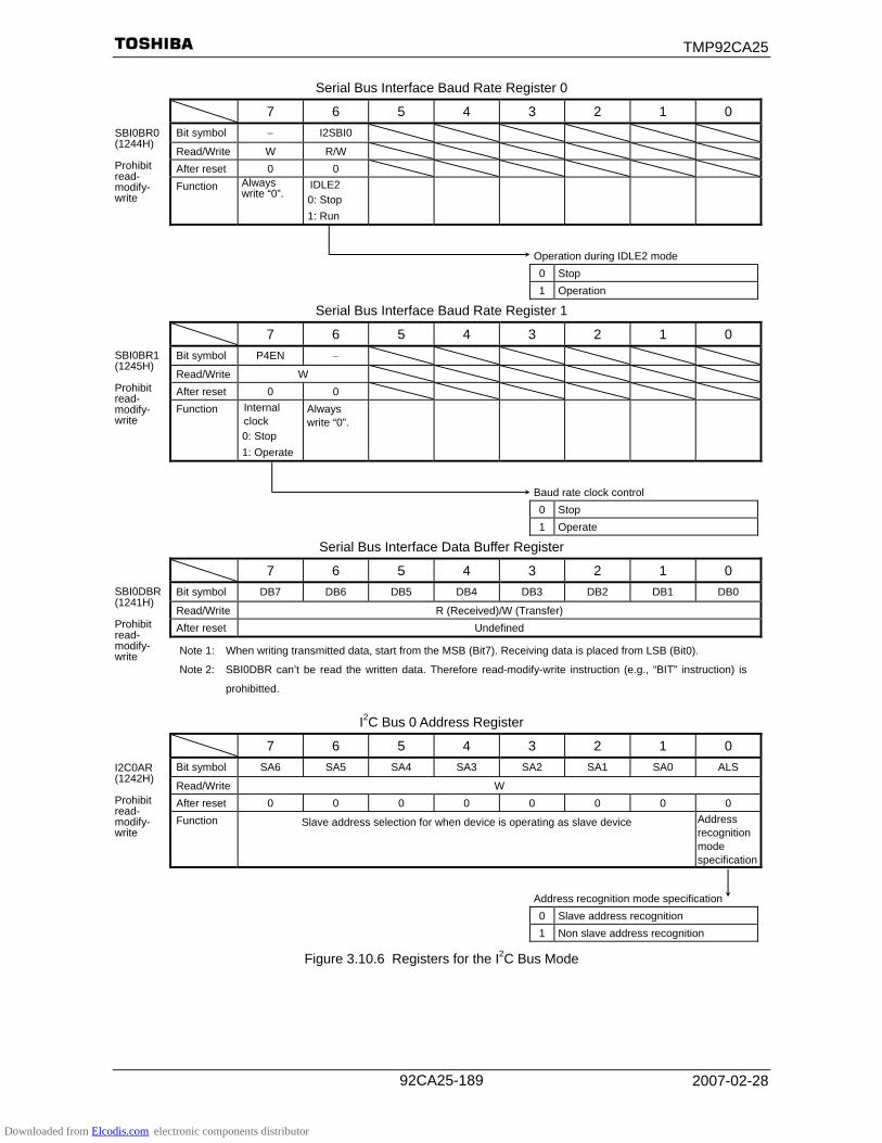
TMP92CA25
2007-02-28 92CA25-189
Serial Bus Interface Baud Rate Register 0
7 6 5 4 3 2 1 0 Bit symbol − I2SBI0
Read/Write W R/W After reset 0 0 Function Always
write “0”. IDLE2 0: Stop 1: Run
Operation during IDLE2 mode 0 Stop 1 Operation
Serial Bus Interface Baud Rate Register 1
7 6 5 4 3 2 1 0 Bit symbol P4EN −
Read/Write W After reset 0 0 Function Internal
clock 0: Stop 1: Operate
Always write “0”.
Baud rate clock control 0 Stop 1 Operate
Serial Bus Interface Data Buffer Register
7 6 5 4 3 2 1 0 Bit symbol DB7 DB6 DB5 DB4 DB3 DB2 DB1 DB0
Read/Write R (Received)/W (Transfer) After reset Undefined
Note 1: When writing transmitted data, start from the MSB (Bit7). Receiving data is placed from LSB (Bit0).
Note 2: SBI0DBR can’t be read the written data. Therefore read-modify-write instruction (e.g., “BIT” instruction) is
prohibitted.
I2C Bus 0 Address Register
7 6 5 4 3 2 1 0 Bit symbol SA6 SA5 SA4 SA3 SA2 SA1 SA0 ALS
Read/Write W After reset 0 0 0 0 0 0 0 0 Function Slave address selection for when device is operating as slave device Address
recognition mode specification
Address recognition mode specification 0 Slave address recognition 1 Non slave address recognition
Figure 3.10.6 Registers for the I2C Bus Mode
SBI0BR0 (1244H) Prohibit read- modify- write
SBI0BR1 (1245H) Prohibit read- modify- write
SBI0DBR (1241H) Prohibit read- modify- write
I2C0AR (1242H) Prohibit read- modify- write
Downloaded from Elcodis.com electronic components distributor

TMP92CA25
2007-02-28 92CA25-190
3.10.5 Control in I2C Bus Mode
(1) Acknowledge mode specification Set the SBI0CR1<ACK> to “1” for operation in the acknowledge mode. The
TMP92CA25 generates an additional clock pulse for an acknowledge signal when operating in master mode. In the transmitter mode during the clock pulse cycle, the SDA pin is released in order to receive the acknowledge signal from the receiver. In the receiver mode during the clock pulse cycle, the SDA pin is set to the low in order to generate the acknowledge signal.
Clear the <ACK> to “0” for operation in the non-acknowledge mode. The TMP92CA25 does not generate a clock pulse for the acknowledge signal when operating in the master mode.
(2) Number of transfer bits Since the SBI0CR1<BC2:0> is cleared to “000” on start up, a slave address and
direction bit transmissions are executed in 8 bits. Other than these, the <BC2:0> retains a specified value.
(3) Serial clock 1. Clock source
The SBI0CR1<SCK2:0> is used to specify the maximum transfer frequency for output on the SCL pin in the master mode. Set the baud rates, which have been calculated according to the formula below, to meet the specifications of the I2C bus, such as the smallest pulse width of tLOW.
SBI0CR1<SCK2:0> n 000 5 001 6 010 7 011 8 100 9 101 10 110 11
Figure 3.10.7 Clock Source
tHIGH tLOW 1/fscl
tLOW = 2n − 1/fSBI tHIGH = 2n−1/fSBI + 8/fSBI fscl = 1/(tLOW + tHIGH)
= fSBI 2n + 8
Note: fSBI is the clock fSYS.
Downloaded from Elcodis.com electronic components distributor

TMP92CA25
2007-02-28 92CA25-191
2. Clock synchronization In the I2C bus mode, in order to wired-AND a bus, a master device which pulls
down a clock pin to the low level, in the first place, invalidate a clock pulse of another master device which generates a high-level clock pulse. The master device with a high-level clock pulse needs to detect the situation and implement the following procedure.
This device has a clock synchronization function which allows normal data transfer even when more than one master exists on the bus.
The following example explains the clock synchronization procedures used when there are two masters present on the bus.
Figure 3.10.8 Clock Synchronization
When master A pulls the internal SCL output to the low level at point “a”, the bus’s SCL pin goes to the low level. After detecting this, master B resets a counter of high-level width of an own clock pulse and sets the internal SCL output the low level.
Master A finishes counting low-level width of an own clock pulse at point “b” and sets the internal SCL output to the high level. Since master B is holding the bus’s SCL pin the low level, master A waits for counting high-level width of an own clock pulse. After master B has finished counting low-level width of an own clock pulse at point “c” and master A detects the SCL pin of the bus at the high level, and starts counting high level of an own clock pulse.
The clock pulse on the bus is determined by the master device with the shortest high-level width and the master device with the longest low-level width from among those master devices connected to the bus.
(4) Slave address and address recognition mode specification When this device is to be used as a slave device, set the slave address <SA6:0> and
<ALS> in I2C0AR. Clear the <ALS> to “0” for the address recognition mode.
(5) Master/slave selection To operate this device as a master device set the SBI0CR2<MST> to “1”. To operate it as a slave device clear the SBI0CR2<MST> to “0”. The <MST> is
cleared to “0” in hardware when a stop condition is detected on the bus or when arbitration is lost.
Start couting high-level width of a clock pulse
Internal SCL output (Master A)
Internal SCL output (Master B)
SCL pin
Wait counting high-levelwidth of a clock pulse
Reset a counter of high-level width of a clock pulse
a b c
Downloaded from Elcodis.com electronic components distributor
TMP92CA25
2007-02-28 92CA25-192
(6) Transmitter/receiver selection To operate this device as a transmitter set the SBI0CR2<TRX> to “1”. To operate it
as a receiver clear the SBI0CR2<TRX> to “0”. When data with an addressing format is transferred in the slave mode, when a slave
address with the same value that an I2C0AR or a GENERAL CALL is received (All 8-bit data are “0” after a start condition), the <TRX> is set to “1” in hardware if the direction bit ( WR/ ) sent from the master device is “1”, and is cleared to “0” in hardware if the bit is “0”.
In the master mode, when an acknowledge signal is returned from the slave device, the <TRX> is cleared to “0” in hardware if the value of the transmitted direction bit is “1”, and is set to “1” in hardware if the value of the bit is “0”. If an acknowledge signal is not returned, the current state is maintained.
The <TRX> is cleared to “0” in hardware when a stop condition is detected on the I2C bus or when arbitration is lost.
(7) Start/stop condition generation When the SBI0SR<BB> = “0”, slave address and direction bit which are set to
SBI0DBR is output on the bus after generating a start condition by writing “1111” to the SBI0CR2<MST, TRX, BB, PIN>. It is necessary to set transmitted data to the data buffer register (SBI0DBR) and set “1” to the <ACK> beforehand.
Figure 3.10.9 Start Condition Generation and Slave Address Generation
When the SBI0SR<BB> = “1”, the sequence for generating a stop condition can be initiated by writing “111” to the SBI0CR2<MST, TRX, PIN> and writing “0” to the SBI0CR2<BB>. Do not modify the contents of the SBI0CR2<MST, TRX, BB, PIN> until a stop condition has been generated on the bus.
Figure 3.10.10 Stop Condition Generation
The state of the bus can be ascertained by reading the contents of the SBI0SR<BB>. The SBI0SR<BB> will be set to “1” if a start condition has been detected on the bus, and will be cleared to “0” if a stop condition has been detected.
Stop condition generation in master mode have limit. Therefore, please refer to 3.10.6 (4) “Stop condition generation”.
1 2 3 4 5 6 7 8 9
A6 A5 A4 A3 A2 A1 A0 R/ W
Slave address and the direction bit Acknowledge signal
Start condition
SCL pin
SDA pin
SCL pin
SDA pin
Stop condition
Downloaded from Elcodis.com electronic components distributor

TMP92CA25
2007-02-28 92CA25-193
(8) Interrupt service requests and interrupt cancellation When a serial bus interface interrupt request 0 by transfer of the slave address or
the data (INTSBI) is generated, the SBI0SR<PIN> is cleared to “0”. The SCL pin is pulled down to the low-level while the <PIN> = “0”.
The <PIN> is cleared to “0” when a single word of data is transmitted or received. Either writing data to or reading data from SBI0DBR sets the <PIN> to “1”.
The time from the <PIN> being set to “1” until the release of the SCL pin is tLOW. In the address recognition mode (e.g., when <ALS> = “0”), the <PIN> is cleared to “0”
when the slave address matches the value set in I2C0AR or when a GENERAL CALL is received (All 8-bit data are “0” after a start condition). Although the SBI0CR2<PIN> can be set to “1” by a program, writing “0” to the SBI0CR2<PIN> does not clear it to “0”.
(9) Serial bus interface operation mode selection The SBI0CR2<SBIM1:0> is used to specify the serial bus interface operation mode. Set the SBI0CR2<SBIM1:0> to “10” when the device is to be used in I2C bus mode
after confirming pin condition of serial bus interface to “H”. Switch a mode to port after confirming a bus is free.
(10) Arbitration lost detection monitor Since more than one master device can exist simultaneously on the bus in I2C bus
mode, a bus arbitration procedure has been implemented in order to guarantee the integrity of transferred data.
Data on the SDA pin is used for I2C bus arbitration. The following example illustrates the bus arbitration procedure when there are two
master devices on the bus. Master A and master B output the same data until point “a”. After master A outputs “L” and master B, “H”, the SDA pin of the bus is wire-AND and the SDA pin is pulled down to the low level by master A. When the SCL pin of the bus is pulled up at point “b”, the slave device reads the data on the SDA pin, that is, data in master A. Data transmitted from master B becomes invalid. The master B state is known as “ARBITRATION LOST”. Master B device which loses arbitration releases the internal SDA output in order not to affect data transmitted from other masters with arbitration. When more than one master sends the same data at the first word, arbitration occurs continuously after the second word.
Figure 3.10.11 Arbitration Lost
Internal SDA output becomes “1” after arbitration has been lost.
SCL pin
Internal SDA output (Master A)
Internal SDA output (Master B)
SDA pin
a b
Downloaded from Elcodis.com electronic components distributor

TMP92CA25
2007-02-28 92CA25-194
This device compares the levels on the bus’s SDA pin with those of the internal SDA output on the rising edge of the SCL pin. If the levels do not match, arbitration is lost and the SBI0SR<AL> is set to “1”.
When the <AL> is set to “1”, the SBI0SR<MST, TRX> are cleared to “00” and the mode is switched to a slave receiver mode. Thus, clock output is stopped in data transfer after setting <AL> = “1”.
The <AL> is cleared to “0” when data is written to or read from SBI0DBR or when data is written to SBI0CR2.
Figure 3.10.12 Example of a Master Device B (D7A = D7B, D6A = D6B)
(11) Slave address match detection monitor The SBI0SR<AAS> is set to “1” in the slave mode, in the address recognition mode
(e.g., when the I2C0AR<ALS> = “0”), when a GENERAL CALL is received, or when a slave address matches the value set in I2C0AR. When the I2C0AR<ALS> = “1”, the SBI0SR<AAS> is set to “1” after the first word of data has been received. The SBI0SR<AAS> is cleared to “0” when data is written to or read from the data buffer register SBI0DBR.
(12) GENERAL CALL detection monitor The SBI0SR<AD0> is set to “1” in the slave mode, when a GENERAL CALL is
received (all 8-bit received data is “0”, after a start condition). The SBI0SR<AD0> is cleared to “0” when a start condition or stop condition is detected on the bus.
(13) Last received bit monitor The value on the SDA pin detected on the rising edge of the SCL pin is stored in the
SBI0SR<LRB>. In the acknowledge mode, immediately after an INTSBI interrupt request has been
generated, an acknowledge signal is read by reading the contents of the SBI0SR<LRB>.
<AL>
<MST>
<TRX>
Stop the clock pulse
1
Keep internal SDA output to high level as losing arbitration
Accessed to SBI0DBR or SBI0CR2
Internal SCL output
Internal SDA output
Internal SDA output
Internal SCL output Master
A
Master B
2 3 4 5 6 7 8 9 1 2 3 4
D7A
D6B
D5A D4A D3A D2A D1A D0A D7A’ D6A’ D5A’ D4A’
1 2 3 4
D7B
D6A
Downloaded from Elcodis.com electronic components distributor

TMP92CA25
2007-02-28 92CA25-195
(14) Software reset function The software reset function is used to initialize the SBI circuit, when SBI is locked by
external noises, etc. An internal reset signal pulse can be generated by setting SBI0CR2<SWRST1:0> to
“10” and “01”. This initializes the SBI circuit internally. All command (except SBI0CR2<SBIM1:0>) registers and status registers are
initialized as well. The SBI0CR1<SWRMON> is automatically set to “1” after the SBI circuit has been
initialized.
(15) Serial bus interface data buffer register (SBI0DBR) The received data can be read and the transferred data can be written by reading or
writing the SBI0DBR. When the start condition has been generated in the master mode, the slave address
and the direction bit are set in this register.
(16) I2C bus address register (I2C0AR) I2C0AR<SA6:0> is used to set the slave address when this device functions as a
slave device. The slave address output from the master device is recognized by setting
I2C0AR<ALS> is set to “0”. The data format is the addressing format. When the slave address in not recognized at the <ALS> is set to “1”, the data format is the free data format.
(17) Baud rate register (SBI0BR1) Write “1” to the SBI0BR1<P4EN> before operation commences.
(18) Setting register for IDLE2 mode operation (SBI0BR0) The setting of SBI0BR0<I2SBI0> determines whether the device is operating or is
stopped in IDLE2 mode. Therefore, setting <I2SBI0> is necessary before the HALT instruction is executed.
Downloaded from Elcodis.com electronic components distributor

TMP92CA25
2007-02-28 92CA25-196
3.10.6 Data Transfer in I2C Bus Mode
(1) Device initialization Set the SBI0BR1<P4EN> and the SBI0CR1<ACK, SCK2:0>. Set the
SBI0BR1<P4EN> to “1” and clear bits 7 to 5 and 3 of the SBI0CR1 to “0”. Set a slave address in I2C0AR<SA6:0> and the I2C0AR<ALS> (<ALS> = “0” when
an addressing format.) For specifying the default setting to a slave receiver mode, clear “000” to the <MST,
TRX, BB>, set “1” to the <PIN>, set “10” to the <SBIM1:0> and set “00” to the <SWRST1:0>.
(2) Start condition and slave address generation 1. Master mode
In the master mode the start condition and the slave address are generated as follows.
Check a bus free status (when <BB> = “0”). Set the SBI0CR1<ACK> to “1” (Acknowledge mode) and specify a slave address
and a direction bit to be transmitted to the SBI0DBR. When the <BB> is ”0”, the start condition is generated by writing “1111” to the
SBI0CR2<MST, TRX, BB, PIN>. Subsequently to the start condition, 9 clocks are output from the SCL pin. While 8 clocks are output, the slave address and the direction bit which are set to the SBI0DBR. At the 9th clock pulse the SDA pin is released and the acknowledge signal is received from the slave device.
An INTSBI interrupt request occurs on the falling edge of the 9th clock pulse. The <PIN> is cleared to “0”. In the master mode the SCL pin is pulled down to the low level while the <PIN> is “0”. When an INTSBI interrupt request occurs, the value of <TRX> is changed according to the direction bit setting only if the slave device returns an acknowledge signal.
2. Slave mode In the slave mode, the start condition and the slave address are received. After the start condition is received from the master device, while 8 clocks are
output from the SCL pin, the slave address and the direction bit which are output from the master device are received.
When a GENERAL CALL or the same address as the slave address set in I2C0AR is received, the SDA line is pulled down to the low level at the 9th clock, and the low level at the 9th clock, and the acknowledge signal is output.
An INTSBI interrupt request occurs on the falling edge of the 9th clock. The <PIN> is cleared to “0”. In slave mode the SCL line is pulled down to the low-level while the <PIN> = “0”.
Downloaded from Elcodis.com electronic components distributor

TMP92CA25
2007-02-28 92CA25-197
Figure 3.10.13 Start Condition Generation and Slave Address Transfer
(3) 1-word data transfer Check the <MST> setting using an INTSBI interrupt process after the transfer of
each word of data is completed and determine whether the device is in the master mode or the slave mode.
1. When the <MST> is “1” (Master mode)
Check the <TRX> setting and determine whether the device is in the transmitter mode or the receiver mode.
When the <TRX> is “1” (Transmitter mode) Check the <LRB> setting. When the <LRB> = “1”, there is no receiver
requesting data. Implement the process for generating a stop condition (See section 3.10.6 (4).) and terminate data transfer.
When the <LRB> = “0”, the receiver is requesting new data. When the next transmitted data is 8 bits, write the transmitted data to the SBI0DBR. When the next transmitted data is other than 8 bits, set the <BC2:0>, set the <ACK> to “1” and write the transmitted data to the SBI0DBR. After the data has been written, the <PIN> is set to “1”, a serial clock pulse is generated to trigger transfer of the next word of data via the SCL pin, and the word is transmitted. After the data has been transmitted, an INTSBI interrupt request is generated. The <PIN> is set to “0” and the SCL pin is pulled down to the low level. If the length of the data to be transferred is greater than one word, repeat the latter steps of the procedure, starting from the check of the <LRB> setting.
Figure 3.10.14 Example in which <BC2:0> = “000” and <ACK> = “1” in Transmitter Mode
1 2 3 4 5 6 7 8 9
A6 A5 A4 A3 A2 A1 ACK R/ W
Slave address + Direction bit
Acknowledge signal from a slave device
Start condition
SCL pin
SDA pin
<PIN>
INTSBI interrupt request
Output of master Output of slave
A0
1 2 3 4 5 6 7 8 9
D7 D6 D5 D4 D3 D2 D1 D0 Acknowledge signal from a receiver
Write to SBI0DBR
SCL pin
SDA pin
<PIN>
INTSBI interrupt request
ACK
Output from master Output from slave
Downloaded from Elcodis.com electronic components distributor
TMP92CA25
2007-02-28 92CA25-198
When the <TRX> is “0” (Receiver mode) When the next transmitted data is other than 8 bits, set the <BC2:0> again.
Set the <ACK> to “1” and read the received data from the SBI0DBR so as to release the SCL pin. (The value of data which is read immediately after a slave address is sent is undefined.) After the data has been read, the <PIN> is set to “1”. Serial clock pulse for transferring new 1 word of data is defined SCL and outputs “L” level from SDA pin with acknowledge timing.
An INTSBI interrupt request is generated and the <PIN> is set to “0”. Then this device pulls down the SCL pin to the low level. This device outputs a clock pulse for 1 word of data transfer and the acknowledge signal each time that received data is read from SBI0DBR.
Figure 3.10.15 Example of when <BC2:0> = “000”, <ACK> = “1” in Receiver Mode
In order to terminate the transmission of data to a transmitter, clear the <ACK> to “0” before reading data which is 1 word before the last data to be received. The last data does not generate a clock pulse for the acknowledge signal. After the data has been transmitted and an interrupt request has been generated, set the <BC2:0> to “001” and read the data. This device generates a clock pulse for a 1-bit data transfer. Since the master device is a receiver, the SDA pin on a bus keeps the high level. The transmitter receives the high-level signal as an ACK signal. The receiver indicates to the transmitter that data transfer is complete.
After 1-bit data is received and an interrupt request has occurred, this device generates a stop condition (See section 3.10.6 (4).) and terminates data transfer.
Figure 3.10.16 Termination of Data Transfer in Master Receiver Mode
1 2 3 4 5 6 7 8 1
D7 D6 D5 D4 D3 D2 D1 D0 Acknowledge signal sent to a transmitter
SCL pin
SDA pin
<PIN>
INTSBI interrupt request
“001” → <BC2:0> read SBI0DBR
“0” → <ACK> read SBI0DBR
9
Output of master Output of slave
1 2 3 4 5 6 7 8 9
D7 D6 D5 D4 D3 D2 D1 D0
Acknowledge signal to a transmitter
Read SBI0DBR
SCL pin
SDA pin
<PIN>
INTSBI interrupt request
New D7
Output from master Output from slave
ACK
Downloaded from Elcodis.com electronic components distributor
TMP92CA25
2007-02-28 92CA25-199
2. When the <MST> is “0” (Slave mode) In the slave mode, this device operates either in normal slave mode or in slave
mode after losing arbitration. In the slave mode, an INTSBI interrupt request occurs when this device
receives a slave address or a GENERAL CALL from the master device, or when a GENERAL CALL is received and data transfer is complete, or after matching a received slave address. In the master mode, this device operates in a slave mode if it is losing arbitration. An INTSBI interrupt request occurs when word data transfer terminates after losing arbitration. When an INTSBI interrupt request occurs, the <PIN> is cleared to “0”, and the SCL pin is pulled down to the low level. Either reading data to or writing data from the SBI0DBR, or setting the <PIN> to “1” releases the SCL pin after taking tLOW time.
Check the SBI0SR<AL>, <TRX>, <AAS>, and <AD0> and implements processes according to conditions listed in the next table.
Downloaded from Elcodis.com electronic components distributor
TMP92CA25
2007-02-28 92CA25-200
Table 3.10.1 Operation in the Slave Mode
<TRX> <AL> <AAS> <AD0> Conditions Process 1 1 0 This device loses arbitration when
transmitting a slave address and receives a slave address of which the value of the direction bit sent from another master is “1”.
1 0 In the slave receiver mode, this device receives a slave address of which the value of the direction bit sent from the master is “1”.
Set the number of bits in 1 word to the <BC2:0> and write the transmitted data to the SBI0DBR.
1
0
0 0 In the slave transmitter mode, 1-word data is transmitted.
Check the <LRB>. If the <LRB> is set to “1”, set the <PIN> to “1” since the receiver does not request the next data. Then, clear the <TRX> to “0” to release the bus. If the <LRB> is cleared to “0”, set the number of bits in a word to the <BC2:0> and write transmitted data to the SBI0DBR since the receiver requests next data.
1 1/0 This device loses arbitration when transmitting a slave address and receives a GENERAL CALL or slave address of which the value of the direction bit sent from another master is “0”.
1
0 0 This device loses arbitration when transmitting a slave address or data and terminates transferring word data.
1 1/0 In the slave receiver mode, this device receives a GENERAL CALL or slave address of which the value of the direction bit sent from the master is “0”.
Read the SBI0DBR for setting the <PIN> to “1” (Reading dummy data) or set the <PIN> to “1”.
0
0
0 1/0 In the slave receiver mode, the device terminates receiving 1-word data.
Set the number of bits in a word to the <BC2:0> and read received data from the SBI0DBR.
Downloaded from Elcodis.com electronic components distributor
TMP92CA25
2007-02-28 92CA25-201
(4) Stop condition generation When the SBI0SR<BB> is “1”, the sequence for generating a stop condition is started
by writing “111” to SBI0CR2<MST, TRX, PIN> and “0” to SBI0CR2<BB>. Do not modify the contents of SBI0CR2<MST, TRX, PIN, BB> until a stop condition is generated on a bus.
When the bus’s SCL line has been pulled down by other devices, this device generates a stop condition when the other device has released the SCL line and the SDA pin rising.
Figure 3.10.17 Stop Condition Generation (Single master)
Figure 3.10.18 Stop Condition Generation (Multi master)
Internal SCL
SDA Pin
<PIN>
<BB> (Read)
Stop condition “1” → <MST> “1” → <TRX> “0” → <BB> “1” → <PIN>
SCL Pin
The case of pulled low by other devices
SCL pin
SDA Pin
<PIN>
<BB> (Read)
Stop condition
“1” → <MST> “1” → <TRX> “0” → <BB> “1” → <PIN>
Internal SCL
Downloaded from Elcodis.com electronic components distributor

TMP92CA25
2007-02-28 92CA25-202
(5) Restart Restart is used during data transfer between a master device and a slave device to
change the data transfer direction. The following description explains how to restart when this device is in the master mode.
Clear the SBI0CR2<MST, TRX, BB> to “000” and set the SBI0CR2<PIN> to “1” to release the bus. The SDA line remains the high level and the SCL pin is released. Since a stop condition is not generated on the bus, other devices assume the bus to be in a busy state. Check the SBI0SR<BB> until it becomes “0” to check that the SCL pin of this device is released. Check the <LRB> until it becomes 1 to check that the SCL line on a bus is not pulled down to the low level by other devices. After confirming that the bus stays in a free state, generate a start condition with procedure described in 3.10.6 (2).
In order to meet setup time when restarting, take at least 4.7 μs of waiting time by software from the time of restarting to confirm that the bus is free until the time to generate the start condition.
Figure 3.10.19 Timing Diagram when Restarting
Start condition
<LRB>
SCL line
Internal SCL output
SDA line
<PIN>
4.7 μs (Min)
<BB>
“0” → <MST>“0” → <TRX>“0” → <BB> “1” → <PIN>
“1” → <MST>“1” → <TRX>“1” → <BB> “1” → <PIN>
9
Downloaded from Elcodis.com electronic components distributor

TMP92CA25
2007-02-28 92CA25-203
3.11 SPIC (SPI Controller)
SPIC is the controller that can be connected to SD card, MMC (Multi Media Card) etc. in SPI mode.
The features as follows.
Double buffer (Transmit/Receive) Generate CRC7 and CRC16 (Transmit/Receive data) Baud Rate : 20Mbps max and 400Kbps min Connect several SD cards and MMC.( Use other output port for SPCS pin as CS ) Use as general clock synchronous SIO
MSB/LSB-first, 8/16bit data length, clock Rising/Falling edge 1 Interrupt : INTSPI
Read, Mask, Clear interrupt and Clear enable can control each 4 interrupts: RFR (Receive buffer of SPIRD: Full), RFW (Transmission buffer of SPITD: Empty), REND (Receive buffer of SPIRS: Full), TEND (Transmission buffer of SPITS: Empty). RFR, RFW can high-speed transaction by micro DMA.
Downloaded from Elcodis.com electronic components distributor

TMP92CA25
2007-02-28 92CA25-204
3.11.1 Block diagram
It shows block diagram and connection to SD card in Figure 3.11.1
Note1: SPCLK, SPCS , SPDO and SPDI pins are set to input port (Port K7, K6, K5, K4) by reset. These signals are needed pull-up
resister to fix voltage level, could you adjust resistance value for your final set.
Note2: Please use general input port or interrupt signal for WP (Write Protect) and CD (Card Detect).
Figure 3.11.1 SPIC Block diagram and Connection example
fSYS Baud rate Generator
SP
IMD
/CT
SPCLK
SP
ITD
SPCS
SP
ITS
Tr
ansm
it ,R
ecei
ve C
ontro
ller SPDO
SP
IRD
SP
IRS
SPDI
SP
IIE/IS
/WE
INTSPI
SP
ICR
SPIC (SPI Controller)
TMP92CA25 SD Card
SCLK
CS
DI
DO
PxxWP (Write Protect)
Pyy/INTyCD (Card Detect)
100KΩ
100KΩ
100KΩ
100KΩ
Inte
rnal
dat
a bu
s
SP
IST
16bit
16bit
16bit
16bit
16bit
16bit
Downloaded from Elcodis.com electronic components distributor

TMP92CA25
2007-02-28 92CA25-205
3.11.2 SFR
SFR of SPIC are as follows. These are connected to CPU with 16bit data bus.
(1) SPIMD (SPI Mode setting register) SPIMD register is for operation mode or clock etc.
SPIMD Register 7 6 5 4 3 2 1 0
bit Symbol XEN CLKSEL2 CLKSEL1 CLKSEL0
Read/Write R/W R/W
After Reset 0 1 0 0
Function
SYSCK 0: disable 1: enable
Select baud rate 000:fSYS 100: fSYS/16 001: fSYS/2 101: fSYS/32 010: fSYS/4 111: fSYS/64
011: fSYS/8 111:Reserved
15 14 13 12 11 10 9 8 bit Symbol LOOPBACK MSB1ST DOSTAT TCPOL RCPOL TDINV RDINV
Read/Write R/W R/W
After Reset 0 1 1 0 0 0 0
Function
LOOPBACK test mode
0:disbale
1:enable
Start bit for transmit/receive
0:LSB
1:MSB
SPDO pin
(no transmit)
0:fixed to ”0”
1:fixed to ”1”
Synchronous clock edge
during transmitting
0: fall
1: rise
Synchronous clock edge
during receiving
0: fall
1: rise
Invert data
During transmitting
0: disable
1: enable
Invert data
During receiving
0: disable
1: enable
Figure 3.11.2 SPIMD Register (a) <LOOPBACK>
Because Internal SPDO can be input to internal SPDI, it can be used as test. Set <XEN>=1 and <LOOPBACK>=1, outputs clock from SPCLK pin regardless of operation of transmit/receive.
Please change the setting when transmitting/receiving is not in operation.
Figure 3.11.3 <LOOPBACK> Register Function (b) <MSB1ST>
Select the start bit of transmit/receive data Please change the setting when transmitting/receiving is not in operation.
(c) <DOSTAT>
Set the status of SPDO pin during no transmitting (after transmitting or during receiving). Please change the setting when transmitting/receiving is not in operation.
Y B
SPDI pin
SPDO pin Transmitting data
Receiving dataA
S
SPIMD<LOOPBACK>
SPIMD (0820H)
(0821H)
Downloaded from Elcodis.com electronic components distributor

TMP92CA25
2007-02-28 92CA25-206
(d) <TCPOL>
Select the edge of synchronous clock during transmitting. Please change the setting during <XEN> = “0”. And set the same value of <RCPOL>.
Figure 3.11.4 <TCPOL> Register function (e) <RCPOL>
Select the edge of synchronous clock during receiving. Please change the setting during <XEN>= “0”. And set the same value of <TCPOL>.
Figure 3.11.5 <TCPOL> Register function (f) <TDINV>
Select logical invert/no invert when output transmitted data from SPDO pin. Please change the setting when transmitting/receiving is not in operation. Data that input to CRC calculation circuit is transmission data that is written to SPITD. This input data is not corresponded to <TDINV>. <TDINV> is not corresponded to <DOSTAT>: it set condition of SPDO pin when it is not
transferred.
(g) <RDINV> Select logical invert/no invert for received data from SPDI pin. Please change the setting when transmitting/receiving is not in operation. Data that input to CRC calculation circuit is selected by <RDINV>.
(h) <XEN> Select the operation for the internal clock.
LSB
SPCLK pin (<TCPOL> = “0”)
SPDO pin Bit0 Bit1 Bit2 Bit3 Bit4 Bit7
MSB
SPCLK pin (<TCPOL>= “1”)
LSB
SPCLK pin (<RCPOL>= “0”)
SPDI pin Bit0 Bit1 Bit2 Bit3 Bit4 Bit7
MSB
SPCLK pin (<RCPOL>= “1”)
Downloaded from Elcodis.com electronic components distributor

TMP92CA25
2007-02-28 92CA25-207
(i) <CLKSEL2:0>
Select baud rate. Baud rate is created from fSYS and settings are in under table. Please change the setting when transmitting/receiving is not in operation.
Table 3.11.1 Example of baud rate
Baud rate [Mbps] <CLKSEL2:0> fSYS =12MHz fSYS =16MHz fSYS =20MHz
fSYS 12 16 20
fSYS/2 6 8 10
fSYS/4 3 4 5
fSYS/8 1.5 2 2.5
fSYS/16 0.75 1 1.25
fSYS/32 0.375 0.5 0.625
fSYS/64 0.1875 0.25 0.3125
Downloaded from Elcodis.com electronic components distributor
TMP92CA25
2007-02-28 92CA25-208
(2) SPICT(SPI Control Register) SPICT register is for data length or CRC etc.
SPICT Register
Figure 3.11.6 SPICT Register (a) <CRC16_7_B>
Select CRC7 or CRC16 to calculate.
(b) <CRCRX_TX_B> Select input data to CRC calculation circuit.
(c) <CRCRESET_B> Initialize CRC calculate register. The process that calculating CRC16 of transmits data and sending CRC next to transmit
data is explained as follows.
1. Set SPICT <CRC16_7_B> for select CRC7 or CRC16 and <CRCRX_TX_B> for select calculating data.
2. For reset SPICR register, write “1” after set <CRCRESET_B> to “0”. 3. Write transmit data to SPITD register, and wait for finish transmission all data. 4. Read SPICR register, and obtain the result of CRC calculation. 5. Transmit CRC which is obtained in (4) by the same way as (3).
CRC calculation of receive data is the same process.
7 6 5 4 3 2 1 0 bit Symbol CEN SPCS_B UNIT16 ALGNEN RXWEN RXUEN
Read/Write R/W R/W
After Reset 0 1 0 0 0 0
Function
communication
control
0: disable
1: enable
SPCS pin
0: output “0”
1: output “1”
Data length
0: 8bit
1: 16bit
Full duplex
alignment
0: disable
1: enable
Sequential receive
0: disable
1: enable
Receive UNIT
0: disable
1: enable
15 14 13 12 11 10 9 8 bit Symbol CRC16_7_B CRCRX_TX_B CRCRESET_B DMAERFW DMAERFR
Read/Write R/W R/W
After Reset 0 0 0 0 0
Function
CRC select
0: CRC7
1: CRC16
CRC data
0: Transmit
1: Receive
CRC calculate register
0:Reset
1:Release
Reset
Micro DMA
0: Disable
1: Enable
Micro DMA
0: Disable
1: Enable
SPICT (0822H) (0822H)
Downloaded from Elcodis.com electronic components distributor
TMP92CA25
2007-02-28 92CA25-209
Figure 3.11.7 Flow chart of CRC calculation
Start
<CRC16_7_B>= “1”, <CRCRX_TX_B>= “0”
<CRCRESET_B>= “0”→“1”
Transmit all data
Read CRC from SPICR
Write CRC to SPITD and send
End
Downloaded from Elcodis.com electronic components distributor

TMP92CA25
2007-02-28 92CA25-210
(d) <DNAERFW> Set clearing interrupt in CPU to unnecessary because be supported RFR interrupt to Micro
DMA. If write “1” to, it be set to one-shot interrupt, clearing interrupt by SPIWE register become to unnecessary. SPIST<RFW> flag generate 1-shot interrupt when change from “0” to “1”(Rising).
(e) <DMAERFR> Set clearing interrupt in CPU to unnecessary because be supported RFR interrupt to Micro
DMA. If write “1” to, it be set to one-shot interrupt, clearing interrupt by SPIWE register become to unnecessary. SPIST<RFR> flag generate 1-shot interrupt when change from “0” to “1”(Rising).
(f) <CEN> Select enable/disable of the pin for SD card or MMC. When the card isn’t inserted or
no-power supply to DVcc, penetrated current is flowed because SPDI pin becomes floating. In addition, current is flowed to the card because SPCS , SPCLK and SPDO pin output “1”. This register can avoid these matters. If write “0” to <CEN> with PKCR and PKFC selecting SPCS , SPCLK, SPDO and SPDI
signal, SPDI pin is prohibit to input (avoiding penetrated current) and SPCS , SPCLK, SPDO pin become high impedance. Please write <CEN> = “1” after card is inserted, supply power to Vcc of card and supply
clock to this circuit (SPIMD<XEN> = “1”).
(g) <SPCS_B> Set the value output to SPCS pin.
(h) <UNIT16> Select the length of transmit/receive data. Data length is described as UNIT downward. Please change the setting when transmitting/receiving is not in operation.
(i) <ALGNEN> Select whether using alignment function for transmit/receive per UNIT during full
duplex. Please change the setting when transmitting/receiving is not in operation.
(j) <RXWEN> Set enable/disable of sequential receiving.
(k) <RXUEN> Set enable/disable of receiving operation per UNIT. In case <RXWEN> = “1”, this bit is not
valid. Please change the setting when transmitting/receiving is not in operation.
Downloaded from Elcodis.com electronic components distributor

TMP92CA25
2007-02-28 92CA25-211
[Transmit / receive operation mode]
It is supported 8 operation modes. They are selected in <ALGNEN>, <RXWEN> and <RXUEN> registers.
Table 3.11.2 transmit/receive operation mode
Register setting Operation mode
<ALGNEN> <RXWEN> <RXUEN>Note
(1) Transmit UNIT 0 0 0 Transmit written data per UNIT (2) Sequential transmit 0 0 0 Transmit written data sequentially (3) Receive UNIT 0 0 1 Receive data of only 1 UNIT (4) Sequential receive 0 1 0 Receive automatically if buffer has
space (5)Transmit/Receive UNIT with no alignment 0 0 1 Transmit/receive 1 UNIT at once with
no alignment per each UNIT (6) Sequential Transmit/Receive UNIT with no alignment
0 1 0 Transmit/receive sequentially at once with no alignment per each UNIT
(7) Transmit/Receive UNIT with alignment 1 0 1 Transmit/receive 1 UNIT with
alignment per each UNIT (8) Sequential Transmit/Receive UNIT with alignment
1 1 0 Transmit/receive sequentially with alignment per each UNIT
Downloaded from Elcodis.com electronic components distributor
TMP92CA25
2007-02-28 92CA25-212
Difference between UNIT transmission and Sequential transmission UNIT transmit mode is transmitted every 1 UNIT by writing data after confirmed
SPIST<TEND>=1.The written transmission data is shifted in turn. In hard ware, transmission is kept executing as long as data exists. If it transmit data sequentially, write next data when SPITD is empty and SPIST<REND>=1.
UNIT transmission and sequential transmission depend on the way of using. Hardware doesn’t depend on.
Figure 3.11.8 show Flow chart of UNIT transmission and Sequential transmission.
Figure 3.11.8 Flow chart of UNIT transmission and Sequential transmission
Y
N
N
N
Y
Y
N
UNIT transmission Sequential transmission
Y
Write transmission data to SPITD
Does SPITS have space? SPIST<TEND>=1?
Does SPITD have space? SPIST<RFW>=1?
Does SPITD have space? SPIST<RFW>=1?
Transmission all data end?
Transmission all data end?
Transmission end? SPIST<TEND>=1?
Transmission end? SPIST<TEND>=1?
Start
Transmission end
Transmission end
Y
N
N
N
Y
Y
Write transmission data to SPITD
Start
Downloaded from Elcodis.com electronic components distributor
TMP92CA25
2007-02-28 92CA25-213
Difference between UNIT receive and Sequential receive UNIT receive is the mode that receiving only 1 UNIT data. By writing “1” to SPICT<RXUEN>, receives 1UNIT data, and received data is loaded in
receive data register (SPIRD). When SPIRD register is read, read it after wrote “0” to SPICT<RXUEN>.
If data was read from SPIRD with the condition SPICT<RXE>= “1”, 1 UNIT data is received again automatically. In hardware, this mode receives sequentially by Single buffer.
SPIST<REND> is changed during UNIT receiving. Sequential receive is the mode that receive data and automatically when receive FIFO has
space. Whenever buffer has space, next data is received automatically. Therefore, if data was read
after data is loaded in SPIRD, it is received sequentially every UNIT. In hardware, this mode receives sequentially by double buffer.
Figure 3.11.9 show Flow chart of UNIT receive and Sequential receive.
Downloaded from Elcodis.com electronic components distributor

TMP92CA25
2007-02-28 92CA25-214
Figure 3.11.9 Flow chart of UNIT receive and Sequential receive
Start
Program receive number -1 Receiving end?
End
Y
N
N
Y
Read receive data from SPIRD
Receiving end? SPIST<RFR>=1?
N
Y
Write “1” to SPICT<RXUEN>
Write “0” to SPICT<RXUEN>
Read last receiving data from SPIRD
Last receiving end? SPIST<RFR>=1?
Start
Program receive number -2 Receiving end?
End
Y
N
N
Y
Read receiving data from SPIRD
N
Y
Write “1” to SPICT<RXWEN>
Write “0” to SPICT<RXWEN>
Read last receiving data from SPIRD
N
Y
N
Y
Read second data from last from SPIRD
Receiving end? SPIST<RFR>=1?
Last second receiving end ? SPIST<RFR>=1?
Last second receiving end ? SPIST<REND>=1?
Does last-data exist in SPIRD? SPIST<RFR>=1?
UNIT receive Sequential receive
Downloaded from Elcodis.com electronic components distributor
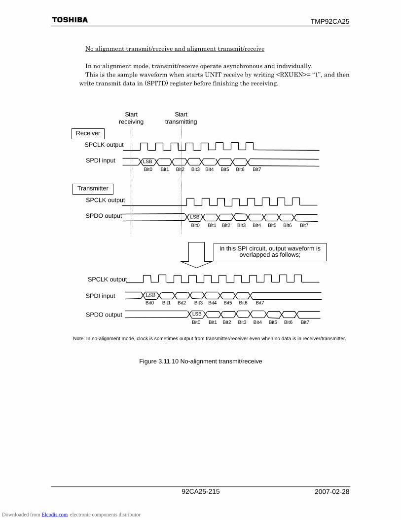
TMP92CA25
2007-02-28 92CA25-215
No alignment transmit/receive and alignment transmit/receive In no-alignment mode, transmit/receive operate asynchronous and individually. This is the sample waveform when starts UNIT receive by writing <RXUEN>= “1”, and then
write transmit data in (SPITD) register before finishing the receiving.
Note: In no-alignment mode, clock is sometimes output from transmitter/receiver even when no data is in receiver/transmitter.
Figure 3.11.10 No-alignment transmit/receive
Bit0 Bit1 Bit2 Bit3 Bit4 Bit5 Bit6 Bit7 LSB
Receiver
SPCLK output
SPDI input
Start receiving
LSB
SPCLK output
SPDO output
Transmitter
SPCLK output
LSB SPDI input
LSBSPDO output
In this SPI circuit, output waveform is overlapped as follows;
Start transmitting
Bit0 Bit1 Bit2 Bit3 Bit4 Bit5 Bit6 Bit7
Bit0 Bit1 Bit2 Bit3 Bit4 Bit5 Bit6 Bit7
Bit0 Bit1 Bit2 Bit3 Bit4 Bit5 Bit6 Bit7
Downloaded from Elcodis.com electronic components distributor

TMP92CA25
2007-02-28 92CA25-216
In alignment mode, it differs from no-alignment mode in transmit/receive is synchronous
every UNIT though it is identical in transmit and receive operate simultaneously. Writing <ALGNEN>= “1” first, and SPICT<RXE>= “1” and keep waiting state for starting
UNIT receiving. When writing SPICT<RXE>= “1” after <ALGNEN>= “1”, receiving does not start right away. This is because the data to transmit at the same time has not been prepared. Transmit/receive start when writing the data to (SPITD) register with the condition <TXE>= “1”.
The waveform of each transmit/receive operation is as follows;
Figure 3.11.11 Alignment transmit/receive
Transmitter
SPCLK output
SPDI input
LSB
SPCLK output
SPDO output
Receiver
LSB
Start receiving
Start transmitting
Bit0 Bit1 Bit2 Bit3 Bit4 Bit5 Bit6 Bit7
Bit0 Bit1 Bit2 Bit3 Bit4 Bit5 Bit6 Bit7
Downloaded from Elcodis.com electronic components distributor
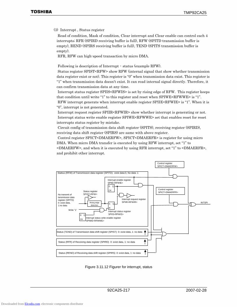
TMP92CA25
2007-02-28 92CA25-217
(3) Interrupt , Status register
Read of condition, Mask of condition, Clear interrupt and Clear enable can control each 4 interrupts; RFR (SPIRD receiving buffer is full), RFW (SPITD transmission buffer is empty), REND (SPIRS receiving buffer is full), TEND (SPITS transmission buffer is empty). RFR, RFW can high-speed transaction by micro DMA. Following is description of Interrupt ・ status (example RFW). Status register SPIST<RFW> show RFW (internal signal that show whether transmission
data register exist or not). This register is “0” when transmission data exist. This register is “1” when transmission data doesn’t exist. It can read internal signal directly. Therefore, it can confirm transmission data at any time. Interrupt status register SPIIS<RFWIS> is set by rising edge of RFW. This register keeps
that condition until write “1” to this register and reset when SPIWE<RFWWE> is “1”. RFW interrupt generate when interrupt enable register SPIIE<RFWIE> is “1”. When it is
“0”, interrupt is not generated. Interrupt request register SPIIR<RFWIR> show whether interrupt is generating or not. Interrupt status write enable register SPIWE<RFWWE> set that enables reset for reset
interrupts status register by mistake. Circuit config of transmission data shift register (SPITS), receiving register (SPIRD),
receiving data shift register (SPIRS) are same with above register. Control register SPICT<DMAERFW>, SPICT<DMAERFR> is register for using micro
DMA. When micro DMA transfer is executed by using RFW interrupt, set “1” to <DMAERFW>, and when it is executed by using RFR interrupt, set “1” to <DMAERFR>, and prohibit other interrupt.
Figure 3.11.12 Figurer for interrupt, status
Interrupt enable register SPIIE<RFWIE> D Q
CK
QS
R
Interrupt status register SPIIS<RFWIS>
Interrupt request register SPIIR<RFWIR>
No transmit of tansmission data register (SPITD) 0: exist data, 1:no data
Write “1”
D Q
CK Interrupt status write enable register SPIWE<RFWWE>
Status (TEND) of Transmission data shift register (SPIST) 0: exist data, 1: no data
Status (RFR) of Receiving data register (SPIRD) 0: exist data, 1: no data
Status (REND) of Receiving data shift register (SPIRS) 0: exist data, 1: no data
Control register SPICT<DMAERFW>
Control register SPICT<DMAERFR> Status register
SPIST<RFW>
Stattus (RFW) of Transmission data register (SPITD): exist data:0, No data: 1
Rising edge detection
INTSPI
Downloaded from Elcodis.com electronic components distributor

TMP92CA25
2007-02-28 92CA25-218
(3-1) SPIST(SPI status register) SPIST shows 4 status.
SPIST Register
7 6 5 4 3 2 1 0 bit Symbol TEND REND RFW RFR
Read/Write R
After Reset 1 0 1 0
Function
Receiving
0:operation
1: no
operation
Receive
Shift register
0: no data
1: exist data
Transmit buffer 0: untransmitted data exist 1: no
untransmitted data
Receive buffer
0:no
valid data
1:valid data
exist
15 14 13 12 11 10 9 8 bit Symbol
Read/Write
After Reset
Function
Figure 3.11.13 SPIST Register
(a) <TEND> This bit is set to “0” when valid data to transmit exists in the shift register for transmit. It
is set to “1” when finish transmitting all the data.
(b) <REND> This bit is set to “0” when receiving is in operation or no valid data exist in receive shift
register. It is set to “1”, when valid data exist in receive read register and keep the data without
shifting. It is cleared to “0”, when CPU read the data and shift to receive read register.
(c) <RFW> After wrote the received data to receive data write register, shift the data to receive data
shift register. It keeps “0” until all valid data has moved. And it is set to “1” when it can accept the next data with no valid data.
(d) <RFR> This bit is set to “1” when received data is shifted from received data shift register to
received data read register and valid data exist. It is set to “0” when the data is read and no valid data.
SPIST (0824H) (0825H)
Downloaded from Elcodis.com electronic components distributor

TMP92CA25
2007-02-28 92CA25-219
(3-2) SPIIS(SPI interrupt status register)
SPIIS register read 4 interrupt status and clear interrupt. This register is cleared to “0” by writing “1” to applicable bit. Status of this register show
interrupt source state. This register can confirm changing of interrupt condition, even if SPI interrupt enable register (SPIIE) is masked.
SPIIS Register 7 6 5 4 3 2 1 0
bit Symbol TENDIS RENDIS RFWIS RFRIS
Read/Write R/W
After Reset 0 0 0 0
Function
Read
0:no interrupt
1:interrupt
Write
0:Don’t care
1:clear
Read
0:no interrupt
1:interrupt
Write
0:Don’t care
1:clear
Read
0:no interrupt
1:interrupt
Write
0:Don’t care
1:clear
Read
0:nointerrupt
1:interrupt
Write
0:Don’t care
1:clear
15 14 13 12 11 10 9 8 bit Symbol
Read/Write
After Reset
Function
Figure 3.11.14 SPIIS Register (a) <TENDIS>
This bit read status of TEND interrupt and clear interrupt. If write this bit, set “1” to SPIWE<TENDWE>.
(b) <REMDIS>
This bit read status of REND interrupt and clear interrupt. If write this bit, set “1” to SPIWE<RENDWE>.
(c) <RFWDIS>
This bit read status of RFW interrupt and clear interrupt. If write this bit, set “1” to SPIWE<RFWWE>.
(d) <RFRIS>
This bit read status of RFR interrupt and clear interrupt. If write this bit, set “1” to SPIWE<RFRWE>.
SPIIS (0828H) (0829H)
Downloaded from Elcodis.com electronic components distributor
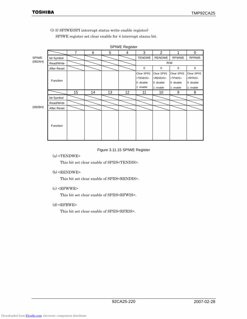
TMP92CA25
2007-02-28 92CA25-220
(3-3) SPIWE(SPI interrupt status write enable register)
SPIWE register set clear enable for 4 interrupt stasus bit.
SPIWE Register 7 6 5 4 3 2 1 0
bit Symbol TENDWE RENDWE RFWWE RFRWE
Read/Write R/W
After Reset 0 0 0 0
Function
Clear SPIIS
<TENDIS>
0: disable
1: enable
Clear SPIIS
<RENDIS>
0: disable
1: enable
Clear SPIIS
<TFWIS>
0: disable
1: enable
Clear SPIIS
<RFRIS>
0: disable
1: enable
15 14 13 12 11 10 9 8 bit Symbol
Read/Write
After Reset
Function
Figure 3.11.15 SPIWE Register (a) <TENDWE>
This bit set clear enable of SPIIS<TENDIS>.
(b) <RENDWE> This bit set clear enable of SPIIS<RENDIS>.
(c) <RFWWE>
This bit set clear enable of SPIIS<RFWIS>.
(d) <RFRWE> This bit set clear enable of SPIIS<RFRIS>.
SPIWE (082AH) (082BH)
Downloaded from Elcodis.com electronic components distributor
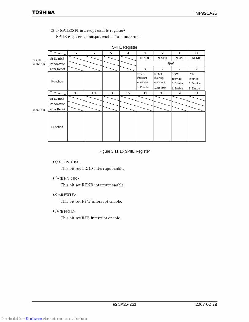
TMP92CA25
2007-02-28 92CA25-221
(3-4) SPIIE(SPI interrupt enable register)
SPIIE register set output enable for 4 interrupt.
SPIIE Register 7 6 5 4 3 2 1 0
bit Symbol TENDIE RENDIE RFWIE RFRIE
Read/Write R/W
After Reset 0 0 0 0
Function
TEND interrupt
0: Disable
1: Enable
REND interrupt
0: Disable
1: Enable
RFW
interrupt
0: Disable
1: Enable
RFR
interrupt
0: Disable
1: Enable
15 14 13 12 11 10 9 8 bit Symbol
Read/Write
After Reset
Function
Figure 3.11.16 SPIIE Register
(a) <TENDIE> This bit set TEND interrupt enable.
(b) <RENDIE>
This bit set REND interrupt enable.
(c) <RFWIE> This bit set RFW interrupt enable.
(d) <RFRIE>
This bit set RFR interrupt enable.
SPIIE (082CH) (082DH)
Downloaded from Elcodis.com electronic components distributor
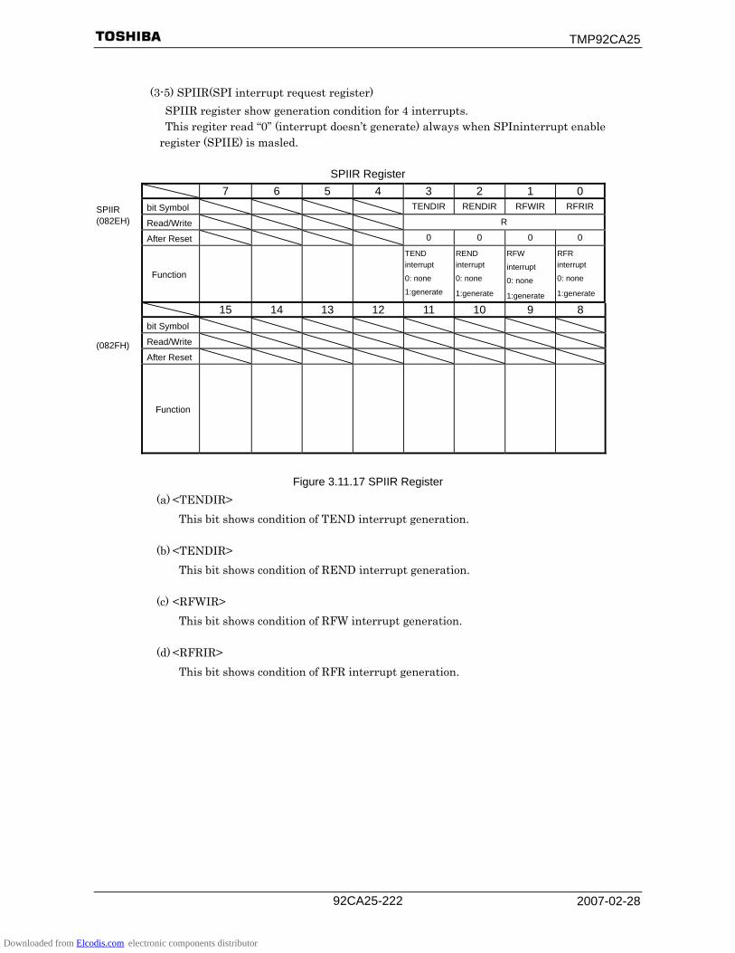
TMP92CA25
2007-02-28 92CA25-222
(3-5) SPIIR(SPI interrupt request register)
SPIIR register show generation condition for 4 interrupts. This regiter read “0” (interrupt doesn’t generate) always when SPIninterrupt enable
register (SPIIE) is masled.
SPIIR Register 7 6 5 4 3 2 1 0
bit Symbol TENDIR RENDIR RFWIR RFRIR
Read/Write R
After Reset 0 0 0 0
Function
TEND interrupt
0: none
1:generate
REND interrupt
0: none
1:generate
RFW
interrupt
0: none
1:generate
RFR interrupt
0: none
1:generate
15 14 13 12 11 10 9 8 bit Symbol
Read/Write
After Reset
Function
Figure 3.11.17 SPIIR Register (a) <TENDIR>
This bit shows condition of TEND interrupt generation.
(b) <TENDIR> This bit shows condition of REND interrupt generation.
(c) <RFWIR> This bit shows condition of RFW interrupt generation.
(d) <RFRIR> This bit shows condition of RFR interrupt generation.
SPIIR (082EH) (082FH)
Downloaded from Elcodis.com electronic components distributor
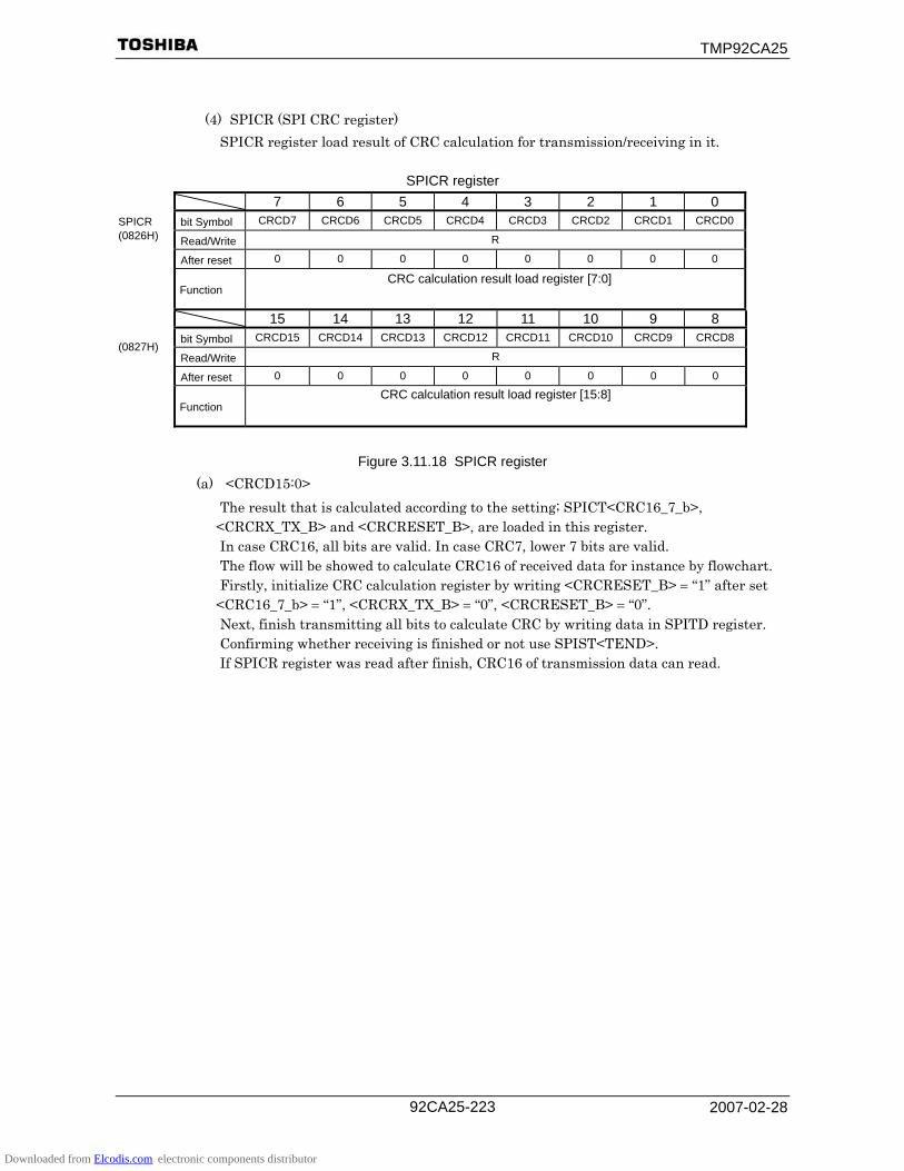
TMP92CA25
2007-02-28 92CA25-223
(4) SPICR (SPI CRC register) SPICR register load result of CRC calculation for transmission/receiving in it.
SPICR register
7 6 5 4 3 2 1 0 bit Symbol CRCD7 CRCD6 CRCD5 CRCD4 CRCD3 CRCD2 CRCD1 CRCD0
Read/Write R
After reset 0 0 0 0 0 0 0 0
Function CRC calculation result load register [7:0]
15 14 13 12 11 10 9 8 bit Symbol CRCD15 CRCD14 CRCD13 CRCD12 CRCD11 CRCD10 CRCD9 CRCD8
Read/Write R
After reset 0 0 0 0 0 0 0 0
Function CRC calculation result load register [15:8]
Figure 3.11.18 SPICR register (a) <CRCD15:0>
The result that is calculated according to the setting; SPICT<CRC16_7_b>, <CRCRX_TX_B> and <CRCRESET_B>, are loaded in this register. In case CRC16, all bits are valid. In case CRC7, lower 7 bits are valid. The flow will be showed to calculate CRC16 of received data for instance by flowchart. Firstly, initialize CRC calculation register by writing <CRCRESET_B> = “1” after set
<CRC16_7_b> = “1”, <CRCRX_TX_B> = “0”, <CRCRESET_B> = “0”. Next, finish transmitting all bits to calculate CRC by writing data in SPITD register. Confirming whether receiving is finished or not use SPIST<TEND>. If SPICR register was read after finish, CRC16 of transmission data can read.
SPICR (0826H) (0827H)
Downloaded from Elcodis.com electronic components distributor
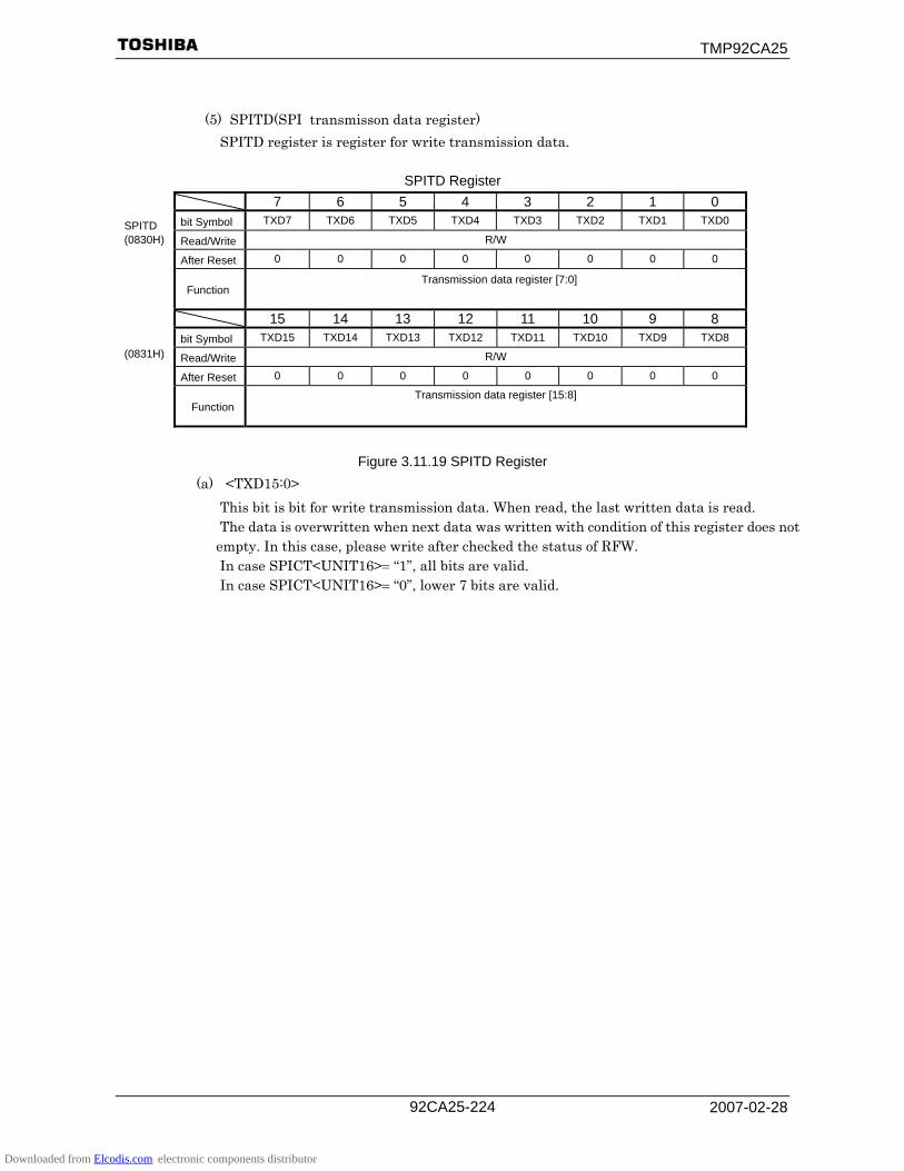
TMP92CA25
2007-02-28 92CA25-224
(5) SPITD(SPI transmisson data register) SPITD register is register for write transmission data.
SPITD Register
7 6 5 4 3 2 1 0 bit Symbol TXD7 TXD6 TXD5 TXD4 TXD3 TXD2 TXD1 TXD0
Read/Write R/W
After Reset 0 0 0 0 0 0 0 0
Function Transmission data register [7:0]
15 14 13 12 11 10 9 8 bit Symbol TXD15 TXD14 TXD13 TXD12 TXD11 TXD10 TXD9 TXD8
Read/Write R/W
After Reset 0 0 0 0 0 0 0 0
Function Transmission data register [15:8]
Figure 3.11.19 SPITD Register (a) <TXD15:0>
This bit is bit for write transmission data. When read, the last written data is read. The data is overwritten when next data was written with condition of this register does not
empty. In this case, please write after checked the status of RFW. In case SPICT<UNIT16>= “1”, all bits are valid. In case SPICT<UNIT16>= “0”, lower 7 bits are valid.
SPITD (0830H) (0831H)
Downloaded from Elcodis.com electronic components distributor

TMP92CA25
2007-02-28 92CA25-225
(6) SPIRD(SPI receiving data register) SPIRD register is register for read receiving data.
SPIRD Register 7 6 5 4 3 2 1 0
bit Symbol RXD7 RXD6 RXD5 RXD4 RXD3 RXD2 RXD1 RXD0
Read/Write R
After Reset 0 0 0 0 0 0 0 0
Function Receive data register [7:0]
15 14 13 12 11 10 9 8 bit Symbol RXD15 RXD14 RXD13 RXD12 RXD11 RXD10 RXD9 RXD8
Read/Write R
After Reset 0 0 0 0 0 0 0 0
Function Receive data register [15:8]
Figure 3.11.20 SPIRD Register
(a) <RXD15:0> SPIRD register is register for reading receiving data. Please read after checked status of
RFK. In case SPICT<UNIT16> = “1”, all bits are valid. In case SPICT<UNIT16> = “0”, lower 7 bits are valid.
SPIRD (0832H) (0833H)
Downloaded from Elcodis.com electronic components distributor

TMP92CA25
2007-02-28 92CA25-226
(7) SPITS (SPI receiving data shift register)
SPITS register change transmission data to serial. This register is used for confirming changing condition when LSI test.
SPITS Register
7 6 5 4 3 2 1 0 bit Symbol TSD7 TSD6 TSD5 TSD4 TSD3 TSD2 TSD1 TSD0
Read/Write R
After Reset 0 0 0 0 0 0 0 0
Function Transmit data shift register [7:0]
15 14 13 12 11 10 9 8 bit Symbol TSD15 TSD14 TSD13 TSD12 TSD11 TSD10 TSD9 TSD8
Read/Write R
After Reset 0 0 0 0 0 0 0 0
Function Transmit data shift register [15:8]
Figure 3.11.21 SPITS Register (a) <TSD15:0>
This register is register for reading the status of transmission data shift register. In case SPICT<UNIT16>= “1”, all bits are valid. In case SPICT<UNIT16>= “0”, lower 8 bits are valid.
SPITS (0834H)
(0835H)
Downloaded from Elcodis.com electronic components distributor
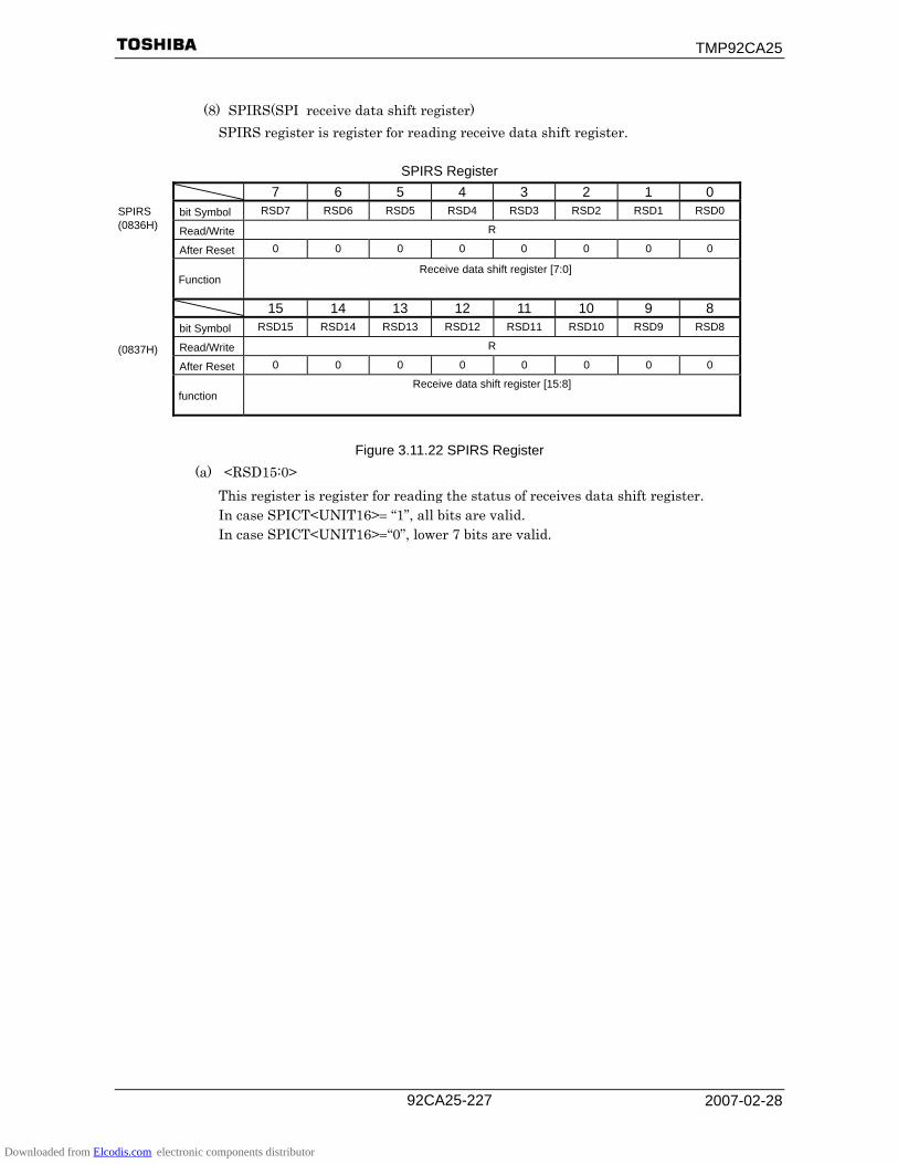
TMP92CA25
2007-02-28 92CA25-227
(8) SPIRS(SPI receive data shift register)
SPIRS register is register for reading receive data shift register.
SPIRS Register 7 6 5 4 3 2 1 0
bit Symbol RSD7 RSD6 RSD5 RSD4 RSD3 RSD2 RSD1 RSD0
Read/Write R
After Reset 0 0 0 0 0 0 0 0
Function Receive data shift register [7:0]
15 14 13 12 11 10 9 8 bit Symbol RSD15 RSD14 RSD13 RSD12 RSD11 RSD10 RSD9 RSD8
Read/Write R
After Reset 0 0 0 0 0 0 0 0
function Receive data shift register [15:8]
Figure 3.11.22 SPIRS Register (a) <RSD15:0>
This register is register for reading the status of receives data shift register. In case SPICT<UNIT16>= “1”, all bits are valid. In case SPICT<UNIT16>=“0”, lower 7 bits are valid.
SPIRS (0836H) (0837H)
Downloaded from Elcodis.com electronic components distributor

TMP92CA25
2007-02-28 92CA25-228
3.11.3 Operation timing
Following examples show operation timing.
• Setting condition 1: Transmission in UNIT=8bit, LSB first
Figure 3.11.23 Transmission timing
In above condition, SPIST<RFW> flag is set to “0” just after wrote transmission data. When data of SPITD register finish shifting to transmission register (SPITS), SPIST<RFW> is set to “1”, it is informed that can write next transmission data, start transmission clock and data from SPCLK pin and SPDO pin at same time with inform.
In this case, SPIIS, SPIIR change and INTSPI interrupt generate by synchronization to rising of SPIST<RFW> flag. When SPIIR register is setting to “1”, interrupt is not generated even if SPIST<RFW> was set to “1”.
When finish transmission and lose data that must to transmit to SPITD register and SPITS register, transmission data and clock are stopped by setting “1” to SPIST<TEND>, and INTSPI interrupt is generated at same time. In this case, if SPIST<TEND> is set to “1” at different interrupt source, INTSPI is not generated. Therefore must to clear SPIIS<RFW> to “0”.
SPCLK pin (<TCPOL>= “0”)
SPDO pin
SPCLK pin (<TCPOL>= “1”)
MSB MSB
SPIIS<TENDIS>
SPIIS<RFWIS>
SPIST<TEND>
SPIST<RFW>
INTSPI Interrupt signal
SPITD Write pulse
SPIIR<RFW> (SPIIE<RFWIE>= “1”)
SPIIS<RFWIS> Clear write pulse
SPIIR<TENDIR> (SPIIE<TENDIE>= “1”)
LSBLSBBit0 Bit1 Bit2 Bit3 Bit4 Bit7 Bit0 Bit1 Bit2 Bit3 Bit4 Bit7
Downloaded from Elcodis.com electronic components distributor

TMP92CA25
2007-02-28 92CA25-229
• Setting condition 2: UNIT transmission in UNIT = 8bit, LSB first
Figure 3.11.24 UNIT receiving (SPICT<RXUEN>=1)
If set SPICT<RXUEN> to “1” without valid receiving data to SPIRD register (SPIST<RFR>=“0”), UNIT receiving is started. When receiving is finished and stored receiving data to SPIRD register, SPIST<RFR> flag is set to “1”, and inform that can read receiving data. Just after read SPIRD register, SPIST<RFR> flag is cleared to “0” and it start receiving next data automatically.
If be finished UNIT receiving, set SPICT<RXUEN> to “0” after confirmed that SPIST<RFR> was set to “1”.
SPIRD Read pulse
SPCLK pin (<RCPOL>= “0”)
SPDI pin
SPCLK pin (<RCPOL>= “1”)
LSB MSB MSB
SPIIS<RENDIS>
SPIIS<RFRIS>
SPIST<REND>
SPIST<RFR>
LSB Bit0 Bit1 Bit2 Bit3 Bit4 Bit7 Bit0 Bit1 Bit2 Bit3 Bit4 Bit7
Downloaded from Elcodis.com electronic components distributor

TMP92CA25
2007-02-28 92CA25-230
• Setting condition 3: Sequential receiving in UNIT=8 bit, LSB first
Figure 3.11.25 continuous receiving (SPICT<RXWEN>=1)
If set SPICT<RXWEN> to “1” without valid receiving data in SPIRD register (SPIST<RFR>=0), sequential receiving is started. When first receiving is finished and stored receiving data to SPIRD register, SPIST<RFR> flag is set to “1”, and inform that can read receiving data. Sequential receiving is received until receiving data is stored to SPIRD and SPIRS registers If finished sequential receiving, set SPICT<RXWEN> to “0” after confirmed that SPIST<REND> was set to “1”.
SPIRD Read pulse
SPCLK pin (<RCPOL>= “0”)
SPDI pin
SPCLK pin (<RCPOL>= “1”)
SPIIS<RENDIS>
SPIST<REND>
SPIST<RFR>
SPIIS<RFRIS>
LSB MSB LSB MSB LSB MSB
Bit0 Bit1 Bit2 Bit3 Bit4 Bit7 Bit0 Bit1 Bit2 Bit3 Bit4 Bit7 Bit0 Bit1 Bit2 Bit3 Bit4 Bit7
Downloaded from Elcodis.com electronic components distributor

TMP92CA25
2007-02-28 92CA25-231
• Setting condition 4: Transmission by using micro DMA in UNIT=8bit, LSB first
Figure 3.11.26 Micro DMA transmission (transmission)
If all bits of SPIIE register are “0” and SPICT<DMAERFW> is “1”, transmission is started by writing transmission data to SPITD register.
If data of SPITD register is shifted to SPITS register and SPIST<RFW> is set to “1” and can write next transmission data, INTSPI interrupt (RFW interrupt) is generated. By starting Micro DMA at this interrupt, can transmit sequential data automatically.
However, If transmit it at Micro DMA, set Micro DMA beforehand.
SPITD Write pulse
SPCLK pin (<TCPOL>= “0”)
SPDO pin
SPCLK pin (<TCPOL>= “1”)
SPIIS<TENDIS>
SPIIS<RFWIS>
SPIST<TEND>
SPIST<RFW>
INTSPI Interrupt pulse
SPIIR<RFWIR>
LSB MSB LSB MSB LSB
Bit0 Bit1 Bit2 Bit3 Bit4 Bit7 Bit0 Bit1 Bit2 Bit3 Bit4 Bit7 Bit0
Downloaded from Elcodis.com electronic components distributor
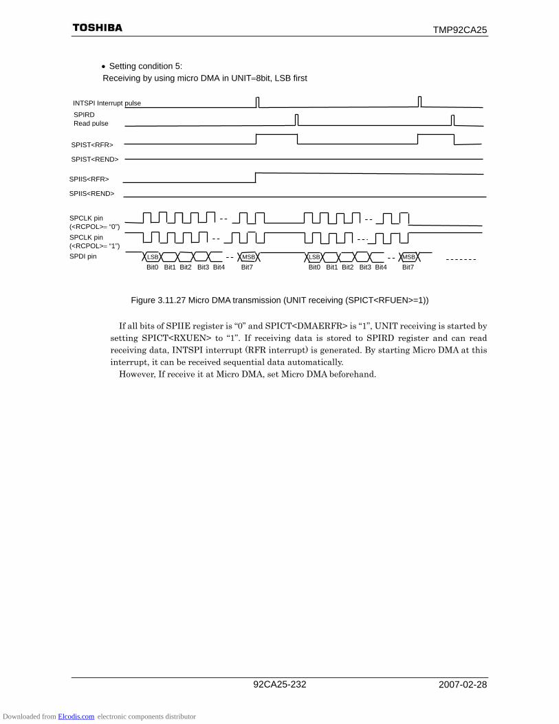
TMP92CA25
2007-02-28 92CA25-232
• Setting condition 5: Receiving by using micro DMA in UNIT=8bit, LSB first
Figure 3.11.27 Micro DMA transmission (UNIT receiving (SPICT<RFUEN>=1)) If all bits of SPIIE register is “0” and SPICT<DMAERFR> is “1”, UNIT receiving is started by
setting SPICT<RXUEN> to “1”. If receiving data is stored to SPIRD register and can read receiving data, INTSPI interrupt (RFR interrupt) is generated. By starting Micro DMA at this interrupt, it can be received sequential data automatically.
However, If receive it at Micro DMA, set Micro DMA beforehand.
SPIRD Read pulse
SPIIS<REND>
SPIIS<RFR>
SPIST<REND>
SPIST<RFR>
INTSPI Interrupt pulse
SPCLK pin (<RCPOL>= “0”)
SPDI pin
SPCLK pin (<RCPOL>= “1”)
LSB MSB LSB MSB
Bit0 Bit1 Bit2 Bit3 Bit4 Bit7 Bit0 Bit1 Bit2 Bit3 Bit4 Bit7
Downloaded from Elcodis.com electronic components distributor
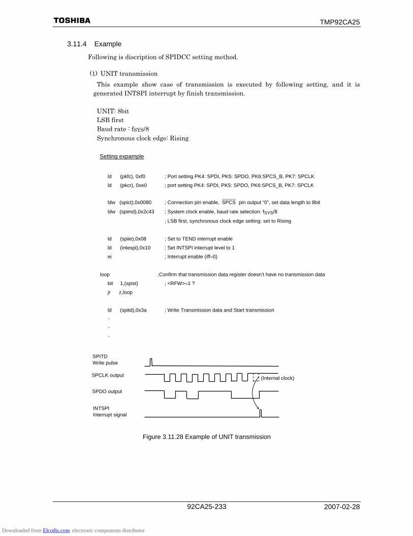
TMP92CA25
2007-02-28 92CA25-233
3.11.4 Example
Following is discription of SPIDCC setting method.
(1) UNIT transmission This example show case of transmission is executed by following setting, and it is
generated INTSPI interrupt by finish transmission.
UNIT: 8bit LSB first Baud rate : fSYS/8 Synchronous clock edge: Rising
Setting expample
ld (pkfc), 0xf0 ; Port setting PK4: SPDI, PK5: SPDO, PK6:SPCS_B, PK7: SPCLK
ld (pkcr), 0xe0 ; port setting PK4: SPDI, PK5: SPDO, PK6:SPCS_B, PK7: SPCLK
ldw (spict),0x0080 ; Connection pin enable, SPCS pin output “0”, set data length to 8bit
ldw (spimd),0x2c43 ; System clock enable, baud rate selection: fSYS/8
; LSB first, synchronous clock edge setting: set to Rising
ld (spiie),0x08 ; Set to TEND interrupt enable
ld (intespi),0x10 ; Set INTSPI interrupt level to 1
ei ; Interrupt enable (iff=0)
loop ;Confirm that transmission data register doesn’t have no transmission data
bit 1,(spist) ; <RFW>=1 ?
jr z,loop
ld (spitd),0x3a ; Write Transmission data and Start transmission
・
・
・
Figure 3.11.28 Example of UNIT transmission
SPCLK output
SPDO output
SPITD Write pulse
INTSPI Interrupt signal
(Internal clock)
Downloaded from Elcodis.com electronic components distributor
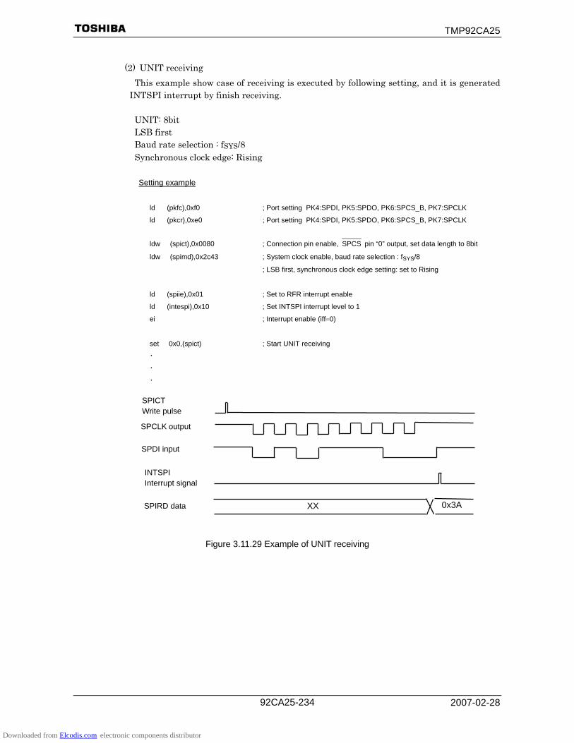
TMP92CA25
2007-02-28 92CA25-234
(2) UNIT receiving
This example show case of receiving is executed by following setting, and it is generated INTSPI interrupt by finish receiving.
UNIT: 8bit LSB first Baud rate selection : fSYS/8 Synchronous clock edge: Rising
Setting example
ld (pkfc),0xf0 ; Port setting PK4:SPDI, PK5:SPDO, PK6:SPCS_B, PK7:SPCLK
ld (pkcr),0xe0 ; Port setting PK4:SPDI, PK5:SPDO, PK6:SPCS_B, PK7:SPCLK
ldw (spict),0x0080 ; Connection pin enable, SPCS pin “0” output, set data length to 8bit
ldw (spimd),0x2c43 ; System clock enable, baud rate selection : fSYS/8
; LSB first, synchronous clock edge setting: set to Rising
ld (spiie),0x01 ; Set to RFR interrupt enable
ld (intespi),0x10 ; Set INTSPI interrupt level to 1
ei ; Interrupt enable (iff=0)
set 0x0,(spict) ; Start UNIT receiving
・
・
・
Figure 3.11.29 Example of UNIT receiving
SPCLK output
SPDI input
SPICT Write pulse
INTSPI Interrupt signal
SPIRD data XX 0x3A
Downloaded from Elcodis.com electronic components distributor
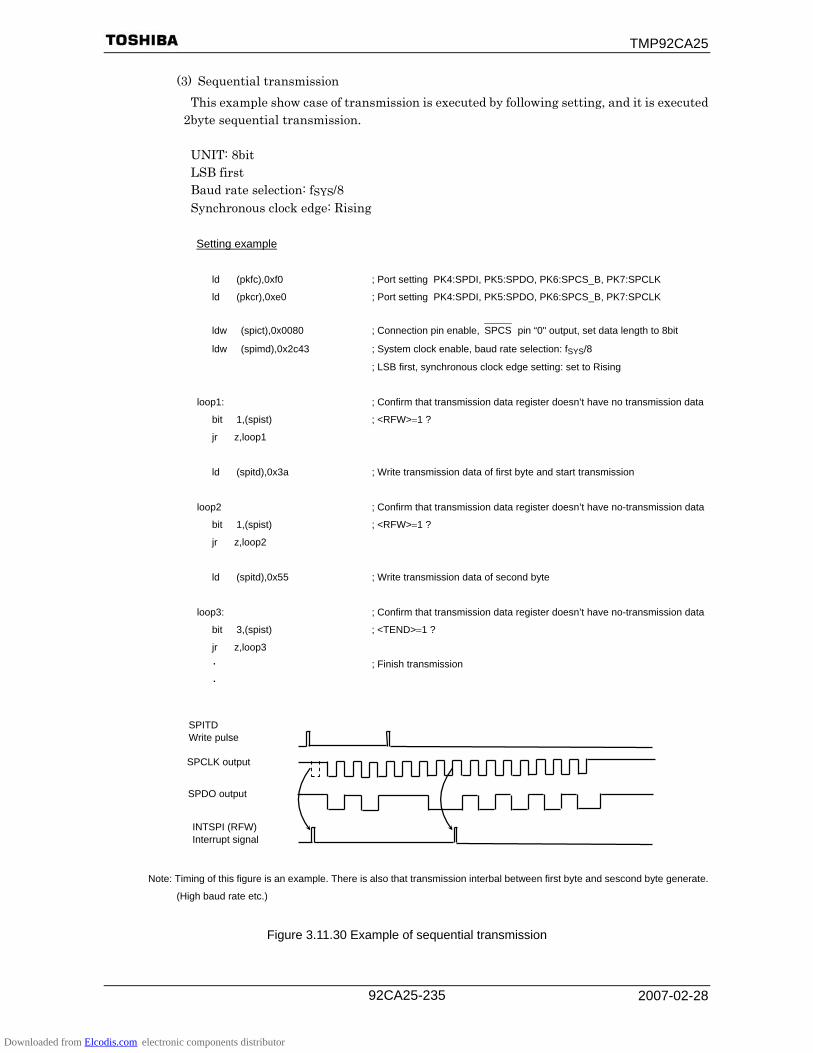
TMP92CA25
2007-02-28 92CA25-235
(3) Sequential transmission This example show case of transmission is executed by following setting, and it is executed
2byte sequential transmission.
UNIT: 8bit LSB first Baud rate selection: fSYS/8 Synchronous clock edge: Rising
Setting example
ld (pkfc),0xf0 ; Port setting PK4:SPDI, PK5:SPDO, PK6:SPCS_B, PK7:SPCLK
ld (pkcr),0xe0 ; Port setting PK4:SPDI, PK5:SPDO, PK6:SPCS_B, PK7:SPCLK
ldw (spict),0x0080 ; Connection pin enable, SPCS pin “0" output, set data length to 8bit
ldw (spimd),0x2c43 ; System clock enable, baud rate selection: fSYS/8
; LSB first, synchronous clock edge setting: set to Rising
loop1: ; Confirm that transmission data register doesn’t have no transmission data
bit 1,(spist) ; <RFW>=1 ?
jr z,loop1
ld (spitd),0x3a ; Write transmission data of first byte and start transmission
loop2 ; Confirm that transmission data register doesn’t have no-transmission data
bit 1,(spist) ; <RFW>=1 ?
jr z,loop2
ld (spitd),0x55 ; Write transmission data of second byte
loop3: ; Confirm that transmission data register doesn’t have no-transmission data
bit 3,(spist) ; <TEND>=1 ?
jr z,loop3
・ ; Finish transmission
・
Note: Timing of this figure is an example. There is also that transmission interbal between first byte and sescond byte generate.
(High baud rate etc.)
Figure 3.11.30 Example of sequential transmission
SPCLK output
SPDO output
SPITD Write pulse
INTSPI (RFW) Interrupt signal
Downloaded from Elcodis.com electronic components distributor
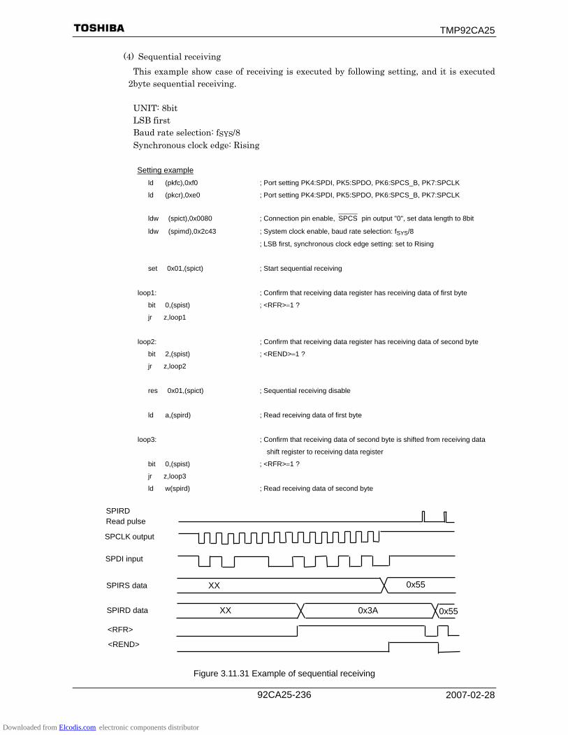
TMP92CA25
2007-02-28 92CA25-236
(4) Sequential receiving This example show case of receiving is executed by following setting, and it is executed
2byte sequential receiving.
UNIT: 8bit LSB first Baud rate selection: fSYS/8 Synchronous clock edge: Rising
Setting example
ld (pkfc),0xf0 ; Port setting PK4:SPDI, PK5:SPDO, PK6:SPCS_B, PK7:SPCLK
ld (pkcr),0xe0 ; Port setting PK4:SPDI, PK5:SPDO, PK6:SPCS_B, PK7:SPCLK
ldw (spict),0x0080 ; Connection pin enable, SPCS pin output "0", set data length to 8bit
ldw (spimd),0x2c43 ; System clock enable, baud rate selection: fSYS/8
; LSB first, synchronous clock edge setting: set to Rising
set 0x01,(spict) ; Start sequential receiving
loop1: ; Confirm that receiving data register has receiving data of first byte
bit 0,(spist) ; <RFR>=1 ?
jr z,loop1
loop2: ; Confirm that receiving data register has receiving data of second byte
bit 2,(spist) ; <REND>=1 ?
jr z,loop2
res 0x01,(spict) ; Sequential receiving disable
ld a,(spird) ; Read receiving data of first byte
loop3: ; Confirm that receiving data of second byte is shifted from receiving data
shift register to receiving data register
bit 0,(spist) ; <RFR>=1 ?
jr z,loop3
ld w(spird) ; Read receiving data of second byte
Figure 3.11.31 Example of sequential receiving
SPCLK output
SPDI input
SPIRD Read pulse
SPIRS data XX
0x3A SPIRD data XX
0x55
0x55
<RFR>
<REND>
Downloaded from Elcodis.com electronic components distributor
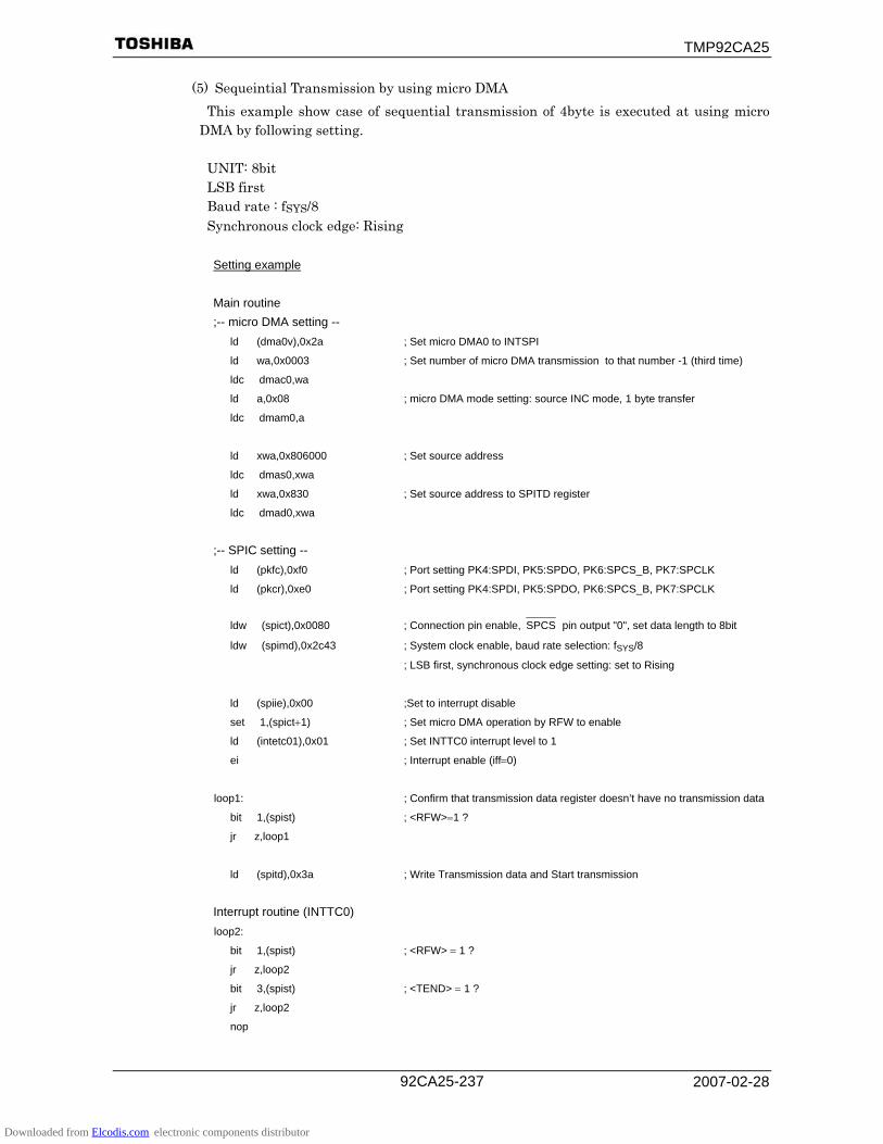
TMP92CA25
2007-02-28 92CA25-237
(5) Sequeintial Transmission by using micro DMA This example show case of sequential transmission of 4byte is executed at using micro
DMA by following setting.
UNIT: 8bit LSB first Baud rate : fSYS/8 Synchronous clock edge: Rising
Setting example Main routine ;-- micro DMA setting --
ld (dma0v),0x2a ; Set micro DMA0 to INTSPI
ld wa,0x0003 ; Set number of micro DMA transmission to that number -1 (third time)
ldc dmac0,wa
ld a,0x08 ; micro DMA mode setting: source INC mode, 1 byte transfer
ldc dmam0,a
ld xwa,0x806000 ; Set source address
ldc dmas0,xwa
ld xwa,0x830 ; Set source address to SPITD register
ldc dmad0,xwa
;-- SPIC setting --
ld (pkfc),0xf0 ; Port setting PK4:SPDI, PK5:SPDO, PK6:SPCS_B, PK7:SPCLK
ld (pkcr),0xe0 ; Port setting PK4:SPDI, PK5:SPDO, PK6:SPCS_B, PK7:SPCLK
ldw (spict),0x0080 ; Connection pin enable, SPCS pin output "0", set data length to 8bit
ldw (spimd),0x2c43 ; System clock enable, baud rate selection: fSYS/8
; LSB first, synchronous clock edge setting: set to Rising
ld (spiie),0x00 ;Set to interrupt disable
set 1,(spict+1) ; Set micro DMA operation by RFW to enable
ld (intetc01),0x01 ; Set INTTC0 interrupt level to 1
ei ; Interrupt enable (iff=0)
loop1: ; Confirm that transmission data register doesn’t have no transmission data
bit 1,(spist) ; <RFW>=1 ?
jr z,loop1
ld (spitd),0x3a ; Write Transmission data and Start transmission
Interrupt routine (INTTC0) loop2:
bit 1,(spist) ; <RFW> = 1 ?
jr z,loop2
bit 3,(spist) ; <TEND> = 1 ?
jr z,loop2
nop
Downloaded from Elcodis.com electronic components distributor

TMP92CA25
2007-02-28 92CA25-238
(6) UNIT receiving by using micro DMA This example show case of UNIT receiving sequentially 4byte is executed at using micro
DMA by following setting. UNIT: 8bit LSB first Baud rate : fSYS/8 Synchronous clock edge: Rising
Setting example Main routine ;-- micro DMA setting --
ld (dma0v),0x2a ; Set micro DMA0 to INTSPI
ld wa,0x0003 ; Set number of micro DMA transmission to that number -1 (third time)
ldc dmac0,wa
ld a,0x00 ; micro DMA mode setting: source INC mode, 1 byte transfer
ldc dmam0,a
ld xwa,0x832 ; Set source address to SPIRD register
ldc dmas0,xwa
ld xwa,0x807000 ; Set source address
ldc dmad0,xwa
;-- SPIC setting --
ld (pkfc),0xf0 ; Port setting PK4:SPDI, PK5:SPDO, PK6:SPCS_B, PK7:SPCLK
ld (pkcr),0xe0 ; Port setting PK4:SPDI, PK5:SPDO, PK6:SPCS_B, PK7:SPCLK
ldw (spict),0x0080 ; Connection pin enable, SPCS pin output “0”, set data length to 8bit
ldw (spimd),0x2c43 ; System clock enable, baud rate selection: fSYS/8
; LSB first, synchronous clock edge setting: set to Rising
ld (spiie),0x00 ; Set to interrupt disable
set 0,(spict+1) ; Set micro DMA operation by RFR to enable
ld (intetc01),0x01 ; Set INTTC0 interrupt level to 1
ei ; Interrupt enable (iff=0)
set 0x0,(spict) ; Start UNIT receiving
Interrupt routine (INTTC0) loop2: ; Wait receiving finish case of UNIT receiving
bit 0,(spist) ; <RFR> = 1 ?
jr z,loop2
res 0,(spict) ; UNIT receiving disable
ld a,(spird) ; Read last receiving data
nop
Downloaded from Elcodis.com electronic components distributor
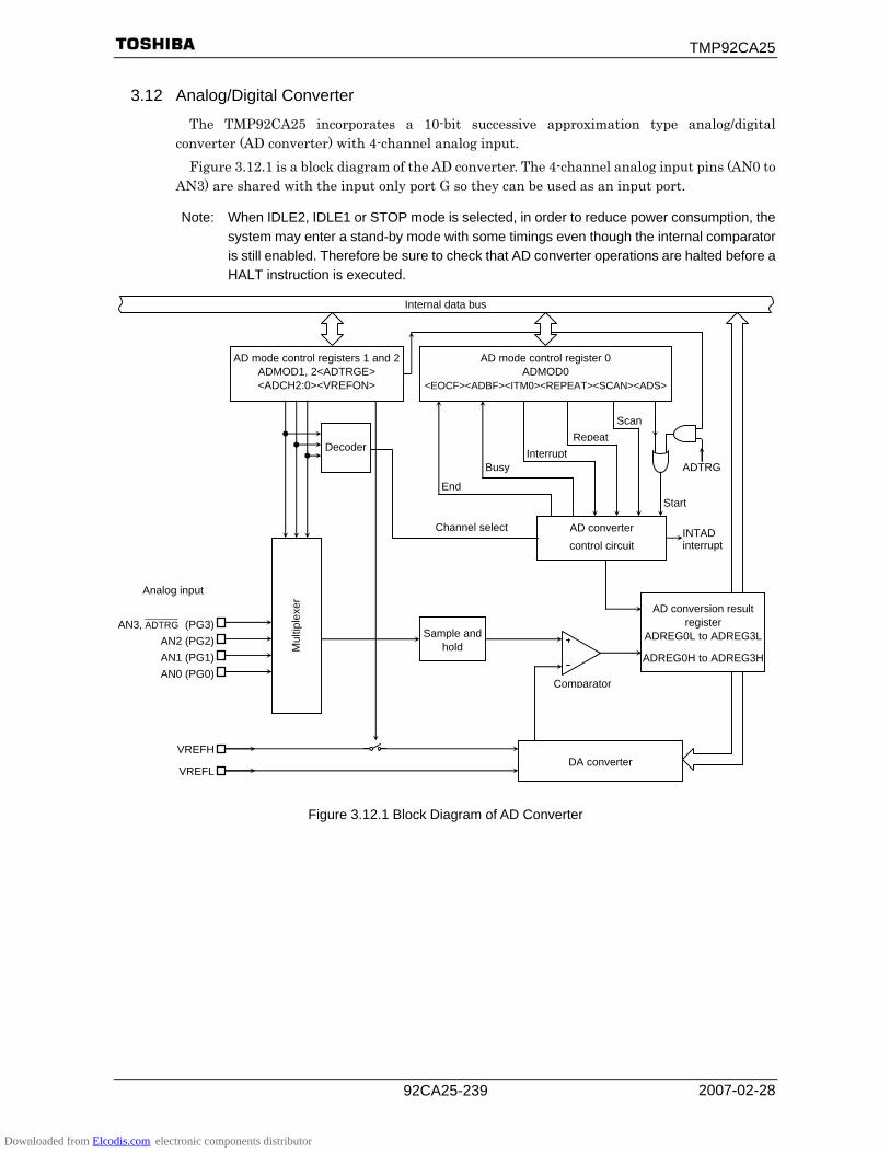
TMP92CA25
2007-02-28 92CA25-239
3.12 Analog/Digital Converter
The TMP92CA25 incorporates a 10-bit successive approximation type analog/digital converter (AD converter) with 4-channel analog input.
Figure 3.12.1 is a block diagram of the AD converter. The 4-channel analog input pins (AN0 to AN3) are shared with the input only port G so they can be used as an input port.
Note: When IDLE2, IDLE1 or STOP mode is selected, in order to reduce power consumption, the system may enter a stand-by mode with some timings even though the internal comparator is still enabled. Therefore be sure to check that AD converter operations are halted before a HALT instruction is executed.
Figure 3.12.1 Block Diagram of AD Converter
Internal data bus
AD mode control register 0 ADMOD0
<EOCF><ADBF><ITM0><REPEAT><SCAN><ADS>
AD mode control registers 1 and 2ADMOD1, 2<ADTRGE> <ADCH2:0><VREFON>
AD converter control circuit
Scan Repeat
InterruptBusy
EndStart
ADTRG
AD conversion result register
ADREG0L to ADREG3L
ADREG0H to ADREG3H
DA converter
Sample and hold M
ultip
lexe
r
Decoder
Comparator
AN3, ADTRG (PG3)AN2 (PG2)AN1 (PG1)AN0 (PG0)
VREFH
VREFL
INTAD interrupt
Channel select
Analog input
Downloaded from Elcodis.com electronic components distributor

TMP92CA25
2007-02-28 92CA25-240
3.12.1 Analog/Digital Converter Registers
The AD converter is controlled by the three AD mode control registers: ADMOD0, ADMOD1 and ADMOD2. The four AD conversion data result registers (ADREG0H/L to ADREG3H/L) store the results of AD conversion.
Figure 3.12.2 shows the registers related to the AD converter.
AD Mode Control Register 0
7 6 5 4 3 2 1 0 Bit symbol EOCF ADBF − − ITM0 REPEAT SCAN ADS ADMOD0
(12B8H) Read/Write R R/W After reset 0 0 0 0 0 0 0 0 Function AD
conversion end flag 0: Conversion
in progress 1: Conversion
complete
AD conversion busy flag 0: Conversion
stopped 1: Conversion
in progress
Always write “0”
Always write “0”
Interrupt specification in conversion channel fixed repeat mode0: Every
conversion1: Every
fourth conversion
Repeat mode specification 0: Single
conversion 1: Repeat
conversion mode
Scan mode specification 0: Conversion
channel fixed mode
1: Conversion channel scan mode
AD conversion start 0: Don’t care1: Start
conversion Always “0” when read
AD conversion start 0 Don’t care 1 Start AD conversion
Note: Always read as “0”.
AD scan mode setting 0 AD conversion channel fixed mode 1 AD conversion channel scan mode
AD repeat mode setting 0 AD single conversion mode 1 AD repeat conversion mode
Specify AD conversion interrupt for channel fixed repeat conversion mode Channel fixed repeat conversion mode
<SCAN> = “0”, <REPEAT> = “1” 0 Generates interrupt every conversion. 1 Generates interrupt every fourth conversion.
AD conversion busy flag 0 AD conversion stopped 1 AD conversion in progress
AD conversion end flag 0 Before or during AD conversion 1 AD conversion complete
Figure 3.12.2 AD Converter Related Register
Downloaded from Elcodis.com electronic components distributor

TMP92CA25
2007-02-28 92CA25-241
AD Mode Control Register 1
7 6 5 4 3 2 1 0 Bit symbol VREFON I2AD − − − − ADCH1 ADCH0 ADMOD1
(12B9H) Read/Write R/W After reset 0 0 0 0 0 0 0 0 Function VREF
application control 0: Off 1: On
IDLE2 0: Stop 1: Operate
Always write “0”
Always write “0”
Always write “0”
Always write “0”
Analog input channel selection
Analog input channel selection <SCAN>
<ADCH1:0>
0 Channel
fixed
1 Channel scanned
00 AN0 AN0 01 AN1 AN0→AN1 10 AN2 AN0→AN1→AN2
11 (Note) AN3 AN0→AN1→AN2→AN3
IDLE2 control 0 Stopped 1 In operation
Control of application of reference voltage to AD converter 0 Off 1 On
Before starting conversion (before writing 1 to ADMOD0<ADS>), set the <VREFON> bit to 1.
AD Mode Control Register 2
7 6 5 4 3 2 1 0 Bit symbol − − − − − − − ADTRGEADMOD2
(12BAH) Read/Write R/W After reset 0 0 0 0 0 0 0 0 Function Always
write “0” Always write “0”
Always write “0”
Always write “0”
Always write “0”
Always write “0”
Always write “0”
AD externaltrigger startcontrol 0: Disable1: Enable
AD conversion start control by external trigger ( ADTRG input) 0 Disabled 1 Enabled
Note: As pin AN3 also functions as the ADTRG input pin, do not set <ADCH1:0> = “11” when using
ADTRG with < ADTRGE > set to “1”.
Figure 3.12.3 AD Converter Related Register
Downloaded from Elcodis.com electronic components distributor

TMP92CA25
2007-02-28 92CA25-242
AD Conversion Result Register 0 Low
7 6 5 4 3 2 1 0 Bit symbol ADR01 ADR00 ADR0RFADREG0L
(12A0H) Read/Write R R After reset Undefined 0 Function Stores lower 2 bits of
AD conversion result. AD conversion
data storage flag
1: Conversion result stored
AD Conversion Result Register 0 High
7 6 5 4 3 2 1 0 Bit symbol ADR09 ADR08 ADR07 ADR06 ADR05 ADR04 ADR03 ADR02 ADREG0H
(12A1H) Read/Write R After reset Undefined Function Stores upper 8 bits of AD conversion result.
AD Conversion Result Register 1 Low
7 6 5 4 3 2 1 0 Bit symbol ADR11 ADR10 ADR1RFADREG1L
(12A2H) Read/Write R R After reset Undefined 0 Function Stores lower 2 bits of
AD conversion result. AD conversion
result flag
1: Conversion result stored
AD Conversion Result Register 1 High
7 6 5 4 3 2 1 0 Bit symbol ADR19 ADR18 ADR17 ADR16 ADR15 ADR14 ADR13 ADR12 ADREG1H
(12A3H) Read/Write R After reset Undefined Function Stores upper 8 bits of AD conversion result.
9 8 7 6 5 4 3 2 1 0
7 6 5 4 3 2 1 0 7 6 5 4 3 2 1 0
• Bits 5 to 1 are always read as 1.
• Bit0 is the AD conversion data storage flag <ADRxRF>.
When the AD conversion result is stored, the flag is set to
1. When either of the registers (ADREGxH, ADREGxL) is
read, the flag is cleared to 0.
Figure 3.12.4 AD Converter Related Registers
ADREGxH ADREGxL
Channel x conversion result
Downloaded from Elcodis.com electronic components distributor

TMP92CA25
2007-02-28 92CA25-243
AD Conversion Result Register 2 Low
7 6 5 4 3 2 1 0 Bit symbol ADR21 ADR20 ADR2RFADREG2L
(12A4H) Read/Write R R After reset Undefined 0 Function Stores lower 2 bits of
AD conversion result. AD conversion
data storage flag
1: Conversion result stored
AD Conversion Result Register 2 High
7 6 5 4 3 2 1 0 Bit symbol ADR29 ADR28 ADR27 ADR26 ADR25 ADR24 ADR23 ADR22 ADREG2H
(12A5H) Read/Write R After reset Undefined Function Stores upper 8 bits of AD conversion result.
AD Conversion Result Register 3 Low
7 6 5 4 3 2 1 0 Bit symbol ADR31 ADR30 ADR3RFADREG3L
(12A6H) Read/Write R R After reset Undefined 0 Function Stores lower 2 bits of
AD conversion result. AD conversion
data storage flag
1: Conversion result stored
AD Conversion Result Register 3 High
7 6 5 4 3 2 1 0 Bit symbol ADR39 ADR38 ADR37 ADR36 ADR35 ADR34 ADR33 ADR32 ADREG3H
(12A7H) Read/Write R After reset Undefined Function Stores upper 8 bits of AD conversion result.
9 8 7 6 5 4 3 2 1 0
7 6 5 4 3 2 1 0 7 6 5 4 3 2 1 0
• Bits 5 to 1 are always read as 1.
• Bit0 is the AD conversion data storage flag <ADRxRF>.
When the AD conversion result is stored, the flag is set to
1. When either of the registers (ADREGxH, ADREGxL) is
read, the flag is cleared to 0.
Figure 3.12.5 AD Converter Related Registers
ADREGxH ADREGxL
Channel x conversion result
Downloaded from Elcodis.com electronic components distributor
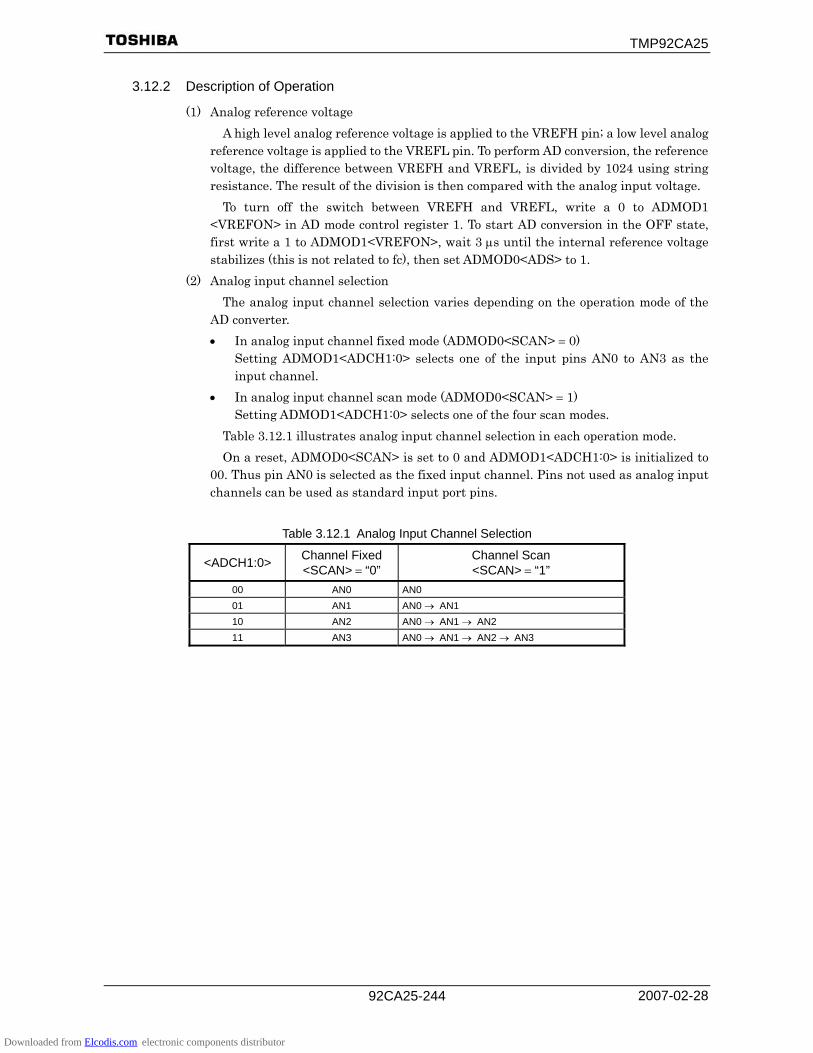
TMP92CA25
2007-02-28 92CA25-244
3.12.2 Description of Operation
(1) Analog reference voltage A high level analog reference voltage is applied to the VREFH pin; a low level analog
reference voltage is applied to the VREFL pin. To perform AD conversion, the reference voltage, the difference between VREFH and VREFL, is divided by 1024 using string resistance. The result of the division is then compared with the analog input voltage.
To turn off the switch between VREFH and VREFL, write a 0 to ADMOD1 <VREFON> in AD mode control register 1. To start AD conversion in the OFF state, first write a 1 to ADMOD1<VREFON>, wait 3 μs until the internal reference voltage stabilizes (this is not related to fc), then set ADMOD0<ADS> to 1.
(2) Analog input channel selection The analog input channel selection varies depending on the operation mode of the
AD converter. • In analog input channel fixed mode (ADMOD0<SCAN> = 0)
Setting ADMOD1<ADCH1:0> selects one of the input pins AN0 to AN3 as the input channel.
• In analog input channel scan mode (ADMOD0<SCAN> = 1) Setting ADMOD1<ADCH1:0> selects one of the four scan modes.
Table 3.12.1 illustrates analog input channel selection in each operation mode. On a reset, ADMOD0<SCAN> is set to 0 and ADMOD1<ADCH1:0> is initialized to
00. Thus pin AN0 is selected as the fixed input channel. Pins not used as analog input channels can be used as standard input port pins.
Table 3.12.1 Analog Input Channel Selection
<ADCH1:0> Channel Fixed <SCAN> = “0”
Channel Scan <SCAN> = “1”
00 AN0 AN0 01 AN1 AN0 → AN1 10 AN2 AN0 → AN1 → AN2 11 AN3 AN0 → AN1 → AN2 → AN3
Downloaded from Elcodis.com electronic components distributor

TMP92CA25
2007-02-28 92CA25-245
(3) Starting AD conversion
To start AD conversion, write a 1 to ADMOD0<ADS> in AD mode control register “0” or ADMOD2<ADTRGE> in AD mode control register 2, and input falling edge on ADTRG pin. When AD conversion starts, the AD conversion busy flag ADMOD0<ADBF> will be set to 1, indicating that AD conversion is in progress.
During AD conversion, a falling edge input on the ADTRG pin will be ignored. (4) AD conversion modes and the AD conversion end interrupt
The four AD conversion modes are: • Channel fixed single conversion mode • Channel scan single conversion mode • Channel fixed repeat conversion mode • Channel scan repeat conversion mode
The ADMOD0<REPEAT> and ADMOD0<SCAN> settings in AD mode control register 0 determine the AD mode setting.
Completion of AD conversion triggers an INTAD AD conversion end interrupt request. Also, ADMOD0<EOCF> will be set to 1 to indicate that AD conversion has been completed. 1. Channel fixed single conversion mode
Setting ADMOD0<REPEAT> and ADMOD0<SCAN> to 00 selects conversion channel fixed single conversion mode.
In this mode, data on one specified channel is converted once only. When the conversion has been completed, the ADMOD0<EOCF> flag is set to 1, ADMOD0<ADBF> is cleared to 0, and an INTAD interrupt request is generated.
2. Channel scan single conversion mode Setting ADMOD0<REPEAT> and ADMOD0<SCAN> to 01 selects conversion
channel scan single conversion mode. In this mode, data on the specified scan channels is converted once only. When
scan conversion has been completed, ADMOD0<EOCF> is set to 1, ADMOD0<ADBF> is cleared to 0, and an INTAD interrupt request is generated.
Downloaded from Elcodis.com electronic components distributor
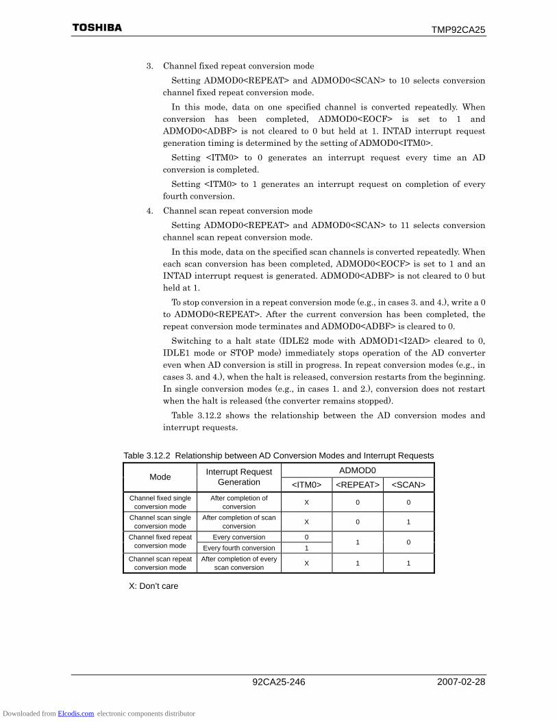
TMP92CA25
2007-02-28 92CA25-246
3. Channel fixed repeat conversion mode
Setting ADMOD0<REPEAT> and ADMOD0<SCAN> to 10 selects conversion channel fixed repeat conversion mode.
In this mode, data on one specified channel is converted repeatedly. When conversion has been completed, ADMOD0<EOCF> is set to 1 and ADMOD0<ADBF> is not cleared to 0 but held at 1. INTAD interrupt request generation timing is determined by the setting of ADMOD0<ITM0>.
Setting <ITM0> to 0 generates an interrupt request every time an AD conversion is completed.
Setting <ITM0> to 1 generates an interrupt request on completion of every fourth conversion.
4. Channel scan repeat conversion mode Setting ADMOD0<REPEAT> and ADMOD0<SCAN> to 11 selects conversion
channel scan repeat conversion mode. In this mode, data on the specified scan channels is converted repeatedly. When
each scan conversion has been completed, ADMOD0<EOCF> is set to 1 and an INTAD interrupt request is generated. ADMOD0<ADBF> is not cleared to 0 but held at 1.
To stop conversion in a repeat conversion mode (e.g., in cases 3. and 4.), write a 0 to ADMOD0<REPEAT>. After the current conversion has been completed, the repeat conversion mode terminates and ADMOD0<ADBF> is cleared to 0.
Switching to a halt state (IDLE2 mode with ADMOD1<I2AD> cleared to 0, IDLE1 mode or STOP mode) immediately stops operation of the AD converter even when AD conversion is still in progress. In repeat conversion modes (e.g., in cases 3. and 4.), when the halt is released, conversion restarts from the beginning. In single conversion modes (e.g., in cases 1. and 2.), conversion does not restart when the halt is released (the converter remains stopped).
Table 3.12.2 shows the relationship between the AD conversion modes and interrupt requests.
Table 3.12.2 Relationship between AD Conversion Modes and Interrupt Requests
ADMOD0 Mode Interrupt Request
Generation <ITM0> <REPEAT> <SCAN> Channel fixed single
conversion mode After completion of
conversion X 0 0
Channel scan single conversion mode
After completion of scan conversion X 0 1
Every conversion 0 Channel fixed repeat conversion mode Every fourth conversion 1
1 0
Channel scan repeat conversion mode
After completion of every scan conversion X 1 1
X: Don’t care
Downloaded from Elcodis.com electronic components distributor

TMP92CA25
2007-02-28 92CA25-247
(5) AD conversion time
84 states (8.4 μs at fSYS = 20 MHz) are required for the AD conversion of one channel. (6) Storing and reading the results of AD conversion
The AD conversion data upper and lower registers (ADREG0H/L to ADREG3H/L) store the results of AD conversion. (ADREG0H/L to ADREG3H/L are read-only registers.)
In channel fixed repeat conversion mode, the conversion results are stored successively in registers ADREG0H/L to ADREG3H/L. In other modes the AN0, AN1, AN2, AN3 and AN4 conversion results are stored in ADREG0H/L, ADREG1H/L, ADREG2H/L and ADREG3H/L respectively.
Table 3.12.3 shows the correspondence between the analog input channels and the registers which are used to hold the results of AD conversion.
Table 3.12.3 Correspondence between Analog Input Channels and AD Conversion Result Registers
AD Conversion Result Register Analog Input Channel
(Port G) Conversion Modes Other than at Right
Channel Fixed Repeat Conversion Mode
(ADMOD0<ITM0 = 1>) AN0 ADREG0H/L ADREG0H/L
AN1 ADREG1H/L ADREG1H/L
AN2 ADREG2H/L ADREG2H/L
AN3 ADREG3H/L ADREG3H/L
<ADRxRF>, bit0 of the AD conversion data lower register, is used as the AD
conversion data storage flag. The storage flag indicates whether the AD conversion result register has been read or not. When a conversion result is stored in the AD conversion result register, the flag is set to 1. When either of the AD conversion result registers (ADREGxH or ADREGxL) is read, the flag is cleared to 0.
Reading the AD conversion result also clears the AD conversion end flag ADMOD0<EOCF> to 0.
Downloaded from Elcodis.com electronic components distributor
TMP92CA25
2007-02-28 92CA25-248
Setting example: 1. Convert the analog input voltage on the AN3 pin and write the result to memory address 2800H using the AD
interrupt (INTAD) processing routine. Main routine: 7 6 5 4 3 2 1 0 INTE0AD ← 1 1 0 0 − − − − Enable INTAD and set it to interrupt level 4. ADMOD1 ← 1 1 0 0 0 0 1 1 Set pin AN3 to be the analog input channel. ADMOD0 ← X X 0 0 0 0 0 1 Start conversion in channel fixed single conversion mode. Interrupt routine processing example: WA ← ADREG3 Read value of ADREG3L and ADREG3H into 16-bits
general-purpose register WA. WA ← > > 6 Shift contents read into WA six times to right and zero fill
upper bits. (2800H) ← WA Write contents of WA to memory address 2800H.
2. This example repeatedly converts the analog input voltages on the three pins AN0, AN1 and AN2, using channel scan repeat conversion mode.
INTE0AD ← 1 0 0 0 − − − − Disable INTAD. ADMOD1 ← 1 1 0 0 0 0 1 0 Set pins AN0 to AN2 to be the analog input channels. ADMOD0 ← X X 0 0 0 1 1 1 Start conversion in channel scan repeat conversion mode. X: Don't care, −: No change
Downloaded from Elcodis.com electronic components distributor
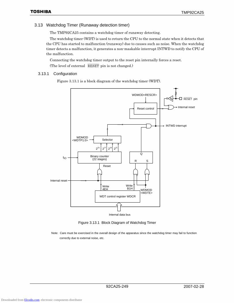
TMP92CA25
2007-02-28 92CA25-249
3.13 Watchdog Timer (Runaway detection timer)
The TMP92CA25 contains a watchdog timer of runaway detecting. The watchdog timer (WDT) is used to return the CPU to the normal state when it detects that
the CPU has started to malfunction (runaway) due to causes such as noise. When the watchdog timer detects a malfunction, it generates a non-maskable interrupt INTWD to notify the CPU of the malfunction.
Connecting the watchdog timer output to the reset pin internally forces a reset. (The level of external RESET pin is not changed.)
3.13.1 Configuration
Figure 3.13.1 is a block diagram of the watchdog timer (WDT).
Figure 3.13.1 Block Diagram of Watchdog Timer
Note: Care must be exercised in the overall design of the apparatus since the watchdog timer may fail to function
correctly due to external noise, etc.
WDMOD<WDTE>
RESET pin
Selector
215 217 219 221
Binary counter (22 stages)
Q
R S
WDT control register WDCR
WriteB1H
Write 4EH
Reset control
WDMOD<RESCR>
Internal reset
INTWD interrupt
Internal reset
fIO
WDMOD<WDTP1:0>
Internal data bus
Reset
Downloaded from Elcodis.com electronic components distributor
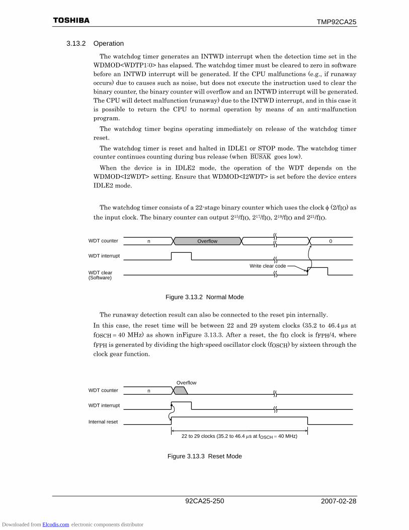
TMP92CA25
2007-02-28 92CA25-250
3.13.2 Operation
The watchdog timer generates an INTWD interrupt when the detection time set in the WDMOD<WDTP1:0> has elapsed. The watchdog timer must be cleared to zero in software before an INTWD interrupt will be generated. If the CPU malfunctions (e.g., if runaway occurs) due to causes such as noise, but does not execute the instruction used to clear the binary counter, the binary counter will overflow and an INTWD interrupt will be generated. The CPU will detect malfunction (runaway) due to the INTWD interrupt, and in this case it is possible to return the CPU to normal operation by means of an anti-malfunction program.
The watchdog timer begins operating immediately on release of the watchdog timer reset.
The watchdog timer is reset and halted in IDLE1 or STOP mode. The watchdog timer counter continues counting during bus release (when BUSAK goes low).
When the device is in IDLE2 mode, the operation of the WDT depends on the WDMOD<I2WDT> setting. Ensure that WDMOD<I2WDT> is set before the device enters IDLE2 mode.
The watchdog timer consists of a 22-stage binary counter which uses the clock φ (2/fIO) as
the input clock. The binary counter can output 215/fIO, 217/fIO, 219/fIO and 221/fIO.
Figure 3.13.2 Normal Mode
The runaway detection result can also be connected to the reset pin internally. In this case, the reset time will be between 22 and 29 system clocks (35.2 to 46.4 μs at fOSCH = 40 MHz) as shown inFigure 3.13.3. After a reset, the fIO clock is fFPH/4, where fFPH is generated by dividing the high-speed oscillator clock (fOSCH) by sixteen through the clock gear function.
Figure 3.13.3 Reset Mode
Overflow n 0 WDT counter
WDT interrupt
WDT clear (Software)
Write clear code
n WDT counter
WDT interrupt
22 to 29 clocks (35.2 to 46.4 μs at fOSCH = 40 MHz)
Overflow
Internal reset
Downloaded from Elcodis.com electronic components distributor

TMP92CA25
2007-02-28 92CA25-251
3.13.3 Control Registers
The watchdog timer (WDT) is controlled by two control registers WDMOD and WDCR. (1) Watchdog timer mode register (WDMOD)
1. Setting the detection time for the watchdog timer in <WDTP1:0> This 2-bit register is used for setting the watchdog timer interrupt time used
when detecting runaway. On a reset this register is initialized to WDMOD<WDTP1:0> = 00. The detection time for WDT is 215/fIO [s]. (The number of system clocks is
approximately 65,536.) 2. Watchdog timer enable/disable control register <WDTE>
At reset, the WDMOD<WDTE> is initialized to 1, enabling the watchdog timer. To disable the watchdog timer, it is necessary to set this bit to 0 and to write the
disable code (B1H) to the watchdog timer control register (WDCR). This makes it difficult for the watchdog timer to be disabled by runaway.
However, it is possible to return the watchdog timer from the disabled state to the enabled state merely by setting <WDTE> to 1.
3. Watchdog timer out reset connection <RESCR> This register is used to connect the output of the watchdog timer with the
RESET terminal internally. Since WDMOD<RESCR> is initialized to 0 at reset, a reset by the watchdog timer will not be performed.
(2) Watchdog timer control register (WDCR) This register is used to disable and clear the binary counter for the watchdog timer.
• Disable control The watchdog timer can be disabled by clearing WDMOD<WDTE> to 0 and then
writing the disable code (B1H) to the WDCR register. WDCR ← 0 1 0 0 1 1 1 0 Write the clear code (4EH). WDMOD ← 0 − − − 0 − − 0 Clear WDMOD <WDTE> to 0. WDCR ← 1 0 1 1 0 0 0 1 Write the disable code (B1H).
• Enable control
Set WDMOD<WDTE> to 1.
• Watchdog timer clear control To clear the binary counter and cause counting to resume, write the clear code
(4EH) to the WDCR register. WDCR ← 0 1 0 0 1 1 1 0 Write the clear code (4EH).
Note1: If the disable control is used, set the disable code (B1H) to WDCR after writing the clear code (4EH) once.
(Please refer to setting example.)
Note2: If the watchdog timer setting is changed, change setting after setting to disable condition once.
Downloaded from Elcodis.com electronic components distributor

TMP92CA25
2007-02-28 92CA25-252
7 6 5 4 3 2 1 0
Bit symbol WDTE WDTP1 WDTP0 − I2WDT RESCR − WDMOD (1300H) Read/Write R/W R/W After reset 1 0 0 0 0 0 0 Function WDT control
1: Enable Select detecting time 00: 215/fIO 01: 217/fIO 10: 219/fIO 11: 221/fIO
Always write “0”
IDLE2 0: Stop 1: Operate
1: Internally connects WDT out to the reset pin
Always write “0”
Watchdog timer out control 0 −
1 Connects WDT out to a reset
IDLE2 control 0 Stop 1 Operation
Watchdog timer detection time 00 215/fIO (Approximately 3.28 ms at fIO = 10 MHz) 01 217/fIO (Approximately 13.1 ms at fIO = 10 MHz) 10 219/fIO (Approximately 52.4 ms at fIO = 10 MHz) 11 221/fIO (Approximately 210 ms at fIO = 10 MHz)
Watchdog timer enable/disable control 0 Disabled 1 Enabled
Figure 3.13.4 Watchdog Timer Mode Register
7 6 5 4 3 2 1 0 Bit symbol − WDCR
(1302H) Read/Write W After reset − Function B1H: WDT disable code
4EH: WDT clear code
WDT disable/clear control B1H Disable code 4EH Clear code
Others Don’t care
Figure 3.13.5 Watchdog Timer Control Register
Read -modify -write instruction is prohibited
Downloaded from Elcodis.com electronic components distributor

TMP92CA25
2007-02-28 92CA25-253
3.14 Real Time Clock (RTC)
3.14.1 Function Description for RTC
1) Clock function (hour, minute, second) 2) Calendar function (month and day, day of the week, and leap year) 3) 24- or 12-hour (AM/PM) clock function 4) +/−30 s adjustment function (by software) 5) Alarm function (alarm output) 6) Alarm interrupt generate
3.14.2 Block Diagram
Figure 3.14.1 RTC Block Diagram
Note 1: Western calendar year column:
This product uses only the final two digits of the year. Therefore, the year following 99 is 00 years. In use, please take into account the first two digits when handling years in the western calendar.
Note 2: Leap year:
A leap year is divisible by 4, but the exception is any leap year which is divisible by 100; this is not considered a leap year. However, any year which is divisible by 400, is a leap year. This product does not take into account the above exceptions . Since this product accounts only for leap years divisible by 4, please adjust the system for any problems.
32-kHz clock Divider
Comparator
Alarm register
Adjust Read/write control
Carry hold (1s)
Address bus
Clock
Alarm select
ALARM INTRTC
16-Hz clock
1-Hz clock
ALARM
Data bus
AddressD0 to D7 WR RD
Downloaded from Elcodis.com electronic components distributor

TMP92CA25
2007-02-28 92CA25-254
3.14.3 Control Registers
Table 3.14.1 PAGE 0 (Clock function) Registers
Symbol Address Bit7 Bit6 Bit5 Bit4 Bit3 Bit2 Bit1 Bit0 Function Read/Write
SECR 1320H 40 sec 20 sec 10 sec 8 sec 4 sec 2 sec 1 sec Second column R/W MINR 1321H 40 min 20 min 10 min 8 min 4 min 2 min 1 min Minute column R/W
HOURR 1322H 20 hours/
PM/AM 10 hours 8 hours 4 hours 2 hours 1 hour Hour column
R/W
DAYR 1323H W2 W1 W0 Day of the week column
R/W
DATER 1324H Day 20 Day 10 Day 8 Day 4 Day 2 Day 1 Day column R/W MONTHR 1325H Oct. Aug. Apr. Feb. Jan. Month column R/W YEARR 1326H Year 80 Year 40 Year 20 Year 10 Year 8 Year 4 Year 2 Year 1
Year column (Lower two columns)
R/W
PAGER 1327H Interrupt enable Adjustment
functionClock enable
Alarm enable
PAGEsetting
PAGE register W, R/W
RESTR 1328H 1Hz enable
16Hz enable
Clock reset
Alarm reset Always write “0” Reset register
W only
Note: When reading SECR, MINR, HOURR, DAYR, MONTHR and YEARR of PAGE0, the current state is read.
Table 3.14.2 PAGE 1 (Alarm function) Registers
Symbol Address Bit7 Bit6 Bit5 Bit4 Bit3 Bit2 Bit1 Bit0 Function Read/Write
SECR 1320H R/W MINR 1321H 40 min 20 min 10 min 8 min 4 min 2 min 1 min Minute column R/W
HOURR 1322H 20 hours/
PM/AM 10 hours 8 hours 4 hours 2 hours 1 hour Hour column
R/W
DAYR 1323H W2 W1 W0 Day of the week column
R/W
DATER 1324H Day 20 Day 10 Day 8 Day 4 Day 2 Day 1 Day column R/W MONTHR 1325H 24/12 24-hour clock mode R/W YEARR 1326H LEAP1 LEAP0 Leap-year mode R/W PAGER 1327H Interrupt
enable Adjustment function
Clock enable
Alarm enable
PAGEsetting
PAGE register W, R/W
RESTR 1328H 1Hz enable
16Hz enable
Clock reset
Alarm reset Always write “0” Reset register
W only
Note: When reading SECR, MINR, HOURR, DAYR, MONTHR, YEARR of PAGE1, the current state is read.
Downloaded from Elcodis.com electronic components distributor

TMP92CA25
2007-02-28 92CA25-255
3.14.4 Detailed Explanation of Control Register
RTC is not initialized by system reset. Therefore, all registers must be initialized at the beginning of the program.
(1) Second column register (for PAGE0 only)
7 6 5 4 3 2 1 0 Bit symbol SE6 SE5 SE4 SE3 SE2 SE1 SE0 SECR
(1320H) Read/Write R/W After reset Undefined Function "0" is read. 40 sec.
column 20 sec. column
10 sec. column
8 sec. column
4 sec. column
2 sec. column
1 sec. column
0 0 0 0 0 0 0 0 sec 0 0 0 0 0 0 1 1 sec 0 0 0 0 0 1 0 2 sec 0 0 0 0 0 1 1 3 sec 0 0 0 0 1 0 0 4 sec 0 0 0 0 1 0 1 5 sec 0 0 0 0 1 1 0 6 sec 0 0 0 0 1 1 1 7 sec 0 0 0 1 0 0 0 8 sec 0 0 0 1 0 0 1 9 sec 0 0 1 0 0 0 0 10 sec
: 0 0 1 1 0 0 1 19 sec 0 1 0 0 0 0 0 20 sec
: 0 1 0 1 0 0 1 29 sec 0 1 1 0 0 0 0 30 sec
: 0 1 1 1 0 0 1 39 sec 1 0 0 0 0 0 0 40 sec
: 1 0 0 1 0 0 1 49 sec 1 0 1 0 0 0 0 50 sec
: 1 0 1 1 0 0 1 59 sec
Note: Do not set data other than as shown above.
Downloaded from Elcodis.com electronic components distributor

TMP92CA25
2007-02-28 92CA25-256
(2) Minute column register (for PAGE0/1)
7 6 5 4 3 2 1 0 Bit symbol MI6 MI5 MI4 MI3 MI2 MI1 MI0 MINR
(1321H) Read/Write R/W After reset Undefined Function “0” is read. 40 min
column 20 min column
10 min column
8 min column
4 min column
2 min column
1 min column
0 0 0 0 0 0 0 0 min 0 0 0 0 0 0 1 1 min 0 0 0 0 0 1 0 2 min 0 0 0 0 0 1 1 3 min 0 0 0 0 1 0 0 4 min 0 0 0 0 1 0 1 5 min 0 0 0 0 1 1 0 6 min 0 0 0 0 1 1 1 7 min 0 0 0 1 0 0 0 8 min 0 0 0 1 0 0 1 9 min 0 0 1 0 0 0 0 10 min
: 0 0 1 1 0 0 1 19 min 0 1 0 0 0 0 0 20 min
: 0 1 0 1 0 0 1 29 min 0 1 1 0 0 0 0 30 min
: 0 1 1 1 0 0 1 39 min 1 0 0 0 0 0 0 40 min
: 1 0 0 1 0 0 1 49 min 1 0 1 0 0 0 0 50 min
: 1 0 1 1 0 0 1 59 min
Note: Do not set data other than as shown above.
Downloaded from Elcodis.com electronic components distributor

TMP92CA25
2007-02-28 92CA25-257
(3) Hour column register (for PAGE0/1)
1. In 24-hour clock mode (MONTHR<MO0> = “1”)
7 6 5 4 3 2 1 0 Bit symbol HO5 HO4 HO3 HO2 HO1 HO0 HOURR
(1322H) Read/Write R/W After reset Undefined Function “0” is read. 20 hours
column 10 hours column
8 hours column
4 hours column
2 hours column
1 hour column
0 0 0 0 0 0 0 o’clock 0 0 0 0 0 1 1 o’clock 0 0 0 0 1 0 2 o’clock
: 0 0 1 0 0 0 8 o’clock 0 0 1 0 0 1 9 o’clock 0 1 0 0 0 0 10 o’clock
: 0 1 1 0 0 1 19 o’clock 1 0 0 0 0 0 20 o’clock
: 1 0 0 0 1 1 23 o’clock
Note: Do not set data other than as shown above.
2. In 12-hour clock mode (MONTHR<MO0> =“0”)
7 6 5 4 3 2 1 0 Bit symbol HO5 HO4 HO3 HO2 HO1 HO0 HOURR
(1322H) Read/Write R/W After reset Undefined Function “0” is read. PM/AM 10 hours
column 8 hours column
4 hours column
2 hours column
1 hour column
0 0 0 0 0 0 0 o’clock (AM)
0 0 0 0 0 1 1 o’clock 0 0 0 0 1 0 2 o’clock :
0 0 1 0 0 1 9 o’clock 0 1 0 0 0 0 10 o’clock 0 1 0 0 0 1 11 o’clock 1 0 0 0 0 0 0 o’clock
(PM) 1 0 0 0 0 1 1 o’clock
Note: Do not set data other than as shown above.
Downloaded from Elcodis.com electronic components distributor

TMP92CA25
2007-02-28 92CA25-258
(4) Day of the week column register (for PAGE0/1)
7 6 5 4 3 2 1 0 Bit symbol WE2 WE1 WE0 DAYR
(1323H) Read/Write R/W After reset Undefined Function “0” is read. W2 W1 W0
0 0 0 Sunday 0 0 1 Monday 0 1 0 Tuesday 0 1 1 Wednesday1 0 0 Thursday 1 0 1 Friday 1 1 0 Saturday
Note: Do not set data other than as shown
above.
(5) Day column register (PAGE0/1)
7 6 5 4 3 2 1 0 Bit symbol DA5 DA4 DA3 DA2 DA1 DA0 DATER
(1324H) Read/Write R/W After reset Undefined Function “0” is read. Day 20 Day 10 Day 8 Day 4 Day 2 Day 1
0 0 0 0 0 0 0 0 0 0 0 0 1 1st day 0 0 0 0 1 0 2nd day 0 0 0 0 1 1 3rd day 0 0 0 1 0 0 4th day
: 0 0 1 0 0 1 9th day 0 1 0 0 0 0 10th day 0 1 0 0 0 1 11th day
: 0 1 1 0 0 1 19th day 1 0 0 0 0 0 20th day
: 1 0 1 0 0 1 29th day 1 1 0 0 0 0 30th day 1 1 0 0 0 1 31st day
Note1: Do not set data other than as shown above.
Note2: Do not set for non-existent days (e.g.: 30th Feb).
Downloaded from Elcodis.com electronic components distributor

TMP92CA25
2007-02-28 92CA25-259
(6) Month column register (for PAGE0 only)
7 6 5 4 3 2 1 0
Bit symbol MO4 MO4 MO2 MO1 MO0 MONTHR (1325H) Read/Write R/W After reset Undefined Function “0” is read. 10 months 8 months 4 months 2 months 1 month
0 0 0 0 1 January 0 0 0 1 0 February 0 0 0 1 1 March 0 0 1 0 0 April 0 0 1 0 1 May 0 0 1 1 0 June 0 0 1 1 1 July 0 1 0 0 0 August 0 1 0 0 1 September1 0 0 0 0 October 1 0 0 0 1 November1 0 0 1 0 December
Note: Do not set data other than as shown above.
(7) Select 24-hour clock or 12-hour clock (for PAGE1 only)
7 6 5 4 3 2 1 0
Bit symbol MO0 MONTHR (1325H) Read/Write R/W After reset Undefined Function
“0” is read. 1: 24-hour0: 12-hour
Downloaded from Elcodis.com electronic components distributor
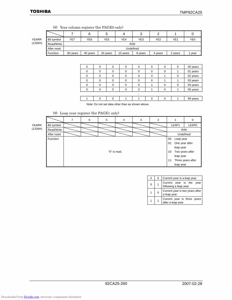
TMP92CA25
2007-02-28 92CA25-260
(8) Year column register (for PAGE0 only)
7 6 5 4 3 2 1 0 Bit symbol YE7 YE6 YE5 YE4 YE3 YE2 YE1 YE0 YEARR
(1326H) Read/Write R/W After reset Undefined Function 80 years 40 years 20 years 10 years 8 years 4 years 2 years 1 year
0 0 0 0 0 0 0 0 00 years 0 0 0 0 0 0 0 1 01 years 0 0 0 0 0 0 1 0 02 years 0 0 0 0 0 0 1 1 03 years 0 0 0 0 0 1 0 0 04 years 0 0 0 0 0 1 0 1 05 years :
1 0 0 1 1 0 0 1 99 years
Note: Do not set data other than as shown above.
(9) Leap year register (for PAGE1 only)
7 6 5 4 3 2 1 0
Bit symbol LEAP1 LEAP0 YEARR (1326H) Read/Write R/W After reset Undefined Function
“0” is read.
00: Leap year 01: One year after leap year 10: Two years after leap year 11: Three years after leap year
0 0 Current year is a leap year
0 1 Current year is the year following a leap year
1 0 Current year is two years after a leap year
1 1 Current year is three years after a leap year
Downloaded from Elcodis.com electronic components distributor

TMP92CA25
2007-02-28 92CA25-261
(10) Setting PAGE register (for PAGE0/1)
7 6 5 4 3 2 1 0
Bit symbol INTENA ADJUST ENATMR ENAALM PAGE PAGER (1327H) Read/Write R/W W R/W R/W After reset 0 Undefined Undefined UndefinedRead-modify-write instruction is prohibited.
Function INTRTC 0: Disable 1: Enable
“0” is read. 0: Don’t
care1: Adjust
Clock 0: Disable 1: Enable
ALARM 0: Disable 1: Enable
“0” is read. PAGE selection
Note: Please keep the setting order below of <ENATMR>, <ENAAML> and <INTENA>. Set different times for
Clock/Alarm setting and interrupt setting.
(Example) Clock setting/Alarm setting ld (pager), 0ch : Clock, Alarm enable ld (pager), 8ch : Interrupt enable
0 Select Page0
PAGE 1 Select Page1
0 Don’t care
ADJUST
1 Adjust sec. counter. When this bit is set to “1” the sec. counter becomes “0” when the value of the sec. counter is 0 – 29. When the value of the sec. counter is 30-59, the min. counter is carried and sec. counter becomes "0". Output Adjust signal during 1 cycle of fSYS. After being adjusted once, Adjust is released automatically. (PAGE0 only)
(11) Setting reset register (for PAGE0/1)
7 6 5 4 3 2 1 0
Bit symbol DIS1Hz DIS16Hz RSTTMR RSTALM − − − − RESTR (1328H) Read/Write W
After reset Undefined Read-modify write-instruction is prohibited.
Function 1Hz 0: Enable 1: Disable
16Hz 0: Enable 1: Disable
1:Clock reset
1: Alarm reset Always write “0”
0 Unused RSTALM
1 Reset alarm register
0 Unused
RSTTMR 1 Reset counter
<DIS1HZ> <DIS1HZ> (PAGER)
<ENAALM> Source signal
1 1 1 Alarm 0 1 0 1Hz 1 0 0 16Hz
Others Output “0”
Downloaded from Elcodis.com electronic components distributor

TMP92CA25
2007-02-28 92CA25-262
3.14.5 Operational description
(1) Reading clock data 1. Using 1Hz interrupt
1Hz interrupt and the count up of internal data synchronize. Therefore, data can read correctly if reading data after 1Hz interrupt occurred.
2. Using two times reading
There is a possibility of incorrect clock data reading when the internal counter carries over. To ensure correct data reading, please read twice, as follows:
Figure 3.14.2 Flowchart of clock data read
Start
END
PAGER<PAGE> = “0” , Select PAGE0
Read the clock data (1st)
Read the clock data (2nd)
1st data = 2nd dataNO
YES
Downloaded from Elcodis.com electronic components distributor

TMP92CA25
2007-02-28 92CA25-263
(2) Writing clock data
When a carry over occurs during a write operation, the data cannot be written correctly. Please use the following method to ensure data is written correctly.
1. Using 1Hz interrupt
1Hz interrupt and the count up of internal data synchronize. Therefore, data can write correctly if writing data after 1Hz interrupt occurred.
2. Resetting a counter
There are 15-stage counter inside the RTC, which generate a 1Hz clock from 32,768 KHz. The data is written after reset this counter.
However, if clearing the counter, it is counted up only first writing at half of the setting time, first writing only. Therefore, if setting the clock counter correctly, after clearing the counter, set the 1Hz-interrupt to enable. And set the time after the first interrupt (occurs at 0.5Hz) is occurred.
Figure 3.14.3 Flowchart of data write
Start
END
PAGER<PAGE> = “0” , Select PAGE0
RESTR<RSTTMR> = “1” reset counter
RESTR<DIS1HZ> = “0” enable 1Hz interrupt
First interrupts occur(After 0.5S)
NO
YES
Sets the time
Downloaded from Elcodis.com electronic components distributor

TMP92CA25
2007-02-28 92CA25-264
2. Disabling the clock
A clock carry over is prohibited when “0” is written to PAGER<ENATMR> in order to prevent malfunction caused by the Carry hold circuit. While the clock is prohibited, the Carry hold circuit holds a one sec. carry signal from a divider. When the clock becomes enabled, the carry signal is output to the clock, the time is revised and operation continues. However, the clock is delayed when clock-disabled state continues for one second or more. Note that at this time system power is down while the clock is disabled. . In this case the clock is stopped and clock is delayed.
Figure 3.14.4 Flowchart of Clock disable
Start
End
Disable the clock
Read the clock data
Enable the clock
Downloaded from Elcodis.com electronic components distributor
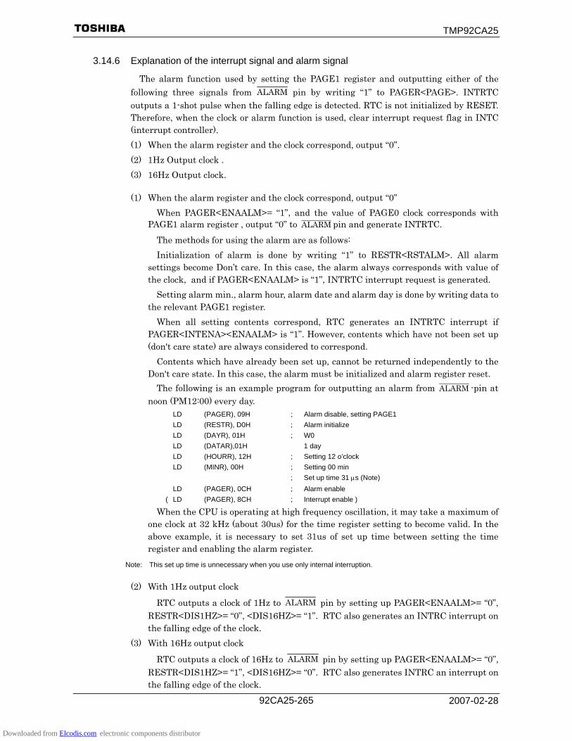
TMP92CA25
2007-02-28 92CA25-265
3.14.6 Explanation of the interrupt signal and alarm signal
The alarm function used by setting the PAGE1 register and outputting either of the following three signals from ALARM pin by writing “1” to PAGER<PAGE>. INTRTC outputs a 1-shot pulse when the falling edge is detected. RTC is not initialized by RESET. Therefore, when the clock or alarm function is used, clear interrupt request flag in INTC (interrupt controller). (1) When the alarm register and the clock correspond, output “0”. (2) 1Hz Output clock . (3) 16Hz Output clock.
(1) When the alarm register and the clock correspond, output “0”
When PAGER<ENAALM>= “1”, and the value of PAGE0 clock corresponds with PAGE1 alarm register , output “0” to ALARM pin and generate INTRTC.
The methods for using the alarm are as follows: Initialization of alarm is done by writing “1” to RESTR<RSTALM>. All alarm
settings become Don’t care. In this case, the alarm always corresponds with value of the clock, and if PAGER<ENAALM> is “1”, INTRTC interrupt request is generated.
Setting alarm min., alarm hour, alarm date and alarm day is done by writing data to the relevant PAGE1 register.
When all setting contents correspond, RTC generates an INTRTC interrupt if PAGER<INTENA><ENAALM> is “1”. However, contents which have not been set up (don't care state) are always considered to correspond.
Contents which have already been set up, cannot be returned independently to the Don't care state. In this case, the alarm must be initialized and alarm register reset.
The following is an example program for outputting an alarm from ALARM -pin at noon (PM12:00) every day.
LD (PAGER), 09H ; Alarm disable, setting PAGE1 LD (RESTR), D0H ; Alarm initialize LD (DAYR), 01H ; W0 LD (DATAR),01H 1 day LD (HOURR), 12H ; Setting 12 o’clock LD (MINR), 00H ; Setting 00 min ; Set up time 31 μs (Note) LD (PAGER), 0CH ; Alarm enable
( LD (PAGER), 8CH ; Interrupt enable )
When the CPU is operating at high frequency oscillation, it may take a maximum of one clock at 32 kHz (about 30us) for the time register setting to become valid. In the above example, it is necessary to set 31us of set up time between setting the time register and enabling the alarm register.
Note: This set up time is unnecessary when you use only internal interruption.
(2) With 1Hz output clock
RTC outputs a clock of 1Hz to ALARM pin by setting up PAGER<ENAALM>= “0”, RESTR<DIS1HZ>= “0”, <DIS16HZ>= “1”. RTC also generates an INTRC interrupt on the falling edge of the clock.
(3) With 16Hz output clock
RTC outputs a clock of 16Hz to ALARM pin by setting up PAGER<ENAALM>= “0”, RESTR<DIS1HZ>= “1”, <DIS16HZ>= “0”. RTC also generates INTRC an interrupt on the falling edge of the clock.
Downloaded from Elcodis.com electronic components distributor

TMP92CA25
2007-02-28 92CA25-266
3.15 LCD Controller
This LSI incorporates two types of liquid crystal display driving circuit for controlling LCDs. One circuit supports an internal RAM LCD driver that can store display data in the LCD driver itself, and the other circuit supports a shift-register type (SR mode) LCD driver that must serially transfer the display data to the LCD driver for each display picture.
It is possible for SR type to use PAN function which is shifted the display without rewriting display data.
1) Shift register type LCD driver control mode (SR mode)
Before setting start register, set the mode of operation, the start address of source data save memory and LCD size to control register.
After setting start register, the LCDC outputs a bus release request to the CPU and reads data from source memory.
The LCDC then transmits LCD size data to the external LCD driver through the special LCDC data bus (LD7to LD0). At this time, the control signals connected to the LCD driver output the specified waveform which is synchronized with the data transmission. After display data reading from RAM is completed, the LCDC cancels the bus release request and the CPU will re-start. It is possible to read the data from display memory at high-speed by FIFO buffer. And it is possible to transfer from LCD-driver-bus corresponded to the AC-standard of connected LCD driver.
In the TMP92CA25, SRAM and SDRAM burst mode can be used for the display RAM. 10-Kbytes of internal RAM are available for use as display RAM. As internal SRAM access is very fast (32-bit bus width, 1 SYSCLK read/write), it is possible to reduce CPU load to a minimum, enabling LCDC DMA. In addition, it can decrease much power consumption during displaying by using internal SRAM. It is possible to display 320×240(QVGA size at max size) using internal SRAM.
2) Internal RAM LCD driver control mode (RAM mode) Data transmission to the LCD driver is executed CPU command. After setting operation
mode to control register, when CPU command is executed the LCDC outputs chip select signal to the LCD driver connected externally by control pin (LCP0 etc.). Therefore control of data transmission numbers corresponding to LCD size is controlled by CPU command.
This mode supports random-access-type and sequential-access-type.
Downloaded from Elcodis.com electronic components distributor

TMP92CA25
2007-02-28 92CA25-267
3.15.1 LCDC features by Mode
The various features and pin operations of are as follows. Table 3.15.1 LCDC features by Mode (example: using TOSHIBA LCD driver)
Shift Register Type LCD Driver Control Mode LCD driver
STN
RAM Built-in Type LCD Driver Control
Mode Display color Monochrome Depends on LCD driver
The number of picture elements which can be handled
Monochrome, 4-, 8- and16-level grayscale Row (Common): 64, 120, 128, 160, 200, 240, 320, 480 Column (Segment):
64, 128, 160, 240, 320, 480, 640
Depends on LCD driver
Data bus width (SRAM, SDRAM) 16 bits, 32 bits (Internal RAM)
Data bus width (Destination: LCD driver) 4 bits, 8 bits
Depends on CS/WAIT controller
(Same as normal memory access)
Maximum transmission rate (at fSYS = 20 [MHz])
12.5 ns/byte at Internal RAM 25 ns/byte at external SRAM, 50 ns/byte at external SRAM, −
Pan function Available to use Depends on LCD driver
LCD data bus LD7 to LD0
Connect to data bus of LCD driver. • 8-bit LD7 to LD0 • 4-bit LD3 to LD0
Not used
D7 to D0 Not used Connect to data bus of LCD driver.
Bus state R/W Not used Connect to WR pin of
LCD driver.
Address bus A0 Not used
Connect to D/I pin of LCD driver for distinction of data or instruction.
LCP0
Shift clock 0 for column LCD driver Connect to CP pin of column LCD driver. LD bus data is latched at falling edge of this signal.
Chip enable signal for column LCD driver Connect to CE pin of 1st column LCD driver.
LLP
Latch pulse output for column and row LCD driver Connect to LP pin of column and row LCD driver. Display data is renewed to output buffer at rising edge of this signal.
Chip enable signal for column LCD driver Connect to CE pin of 2nd column LCD driver.
LFR
Alternating signal for LCD display control. Connect to FR pin of LCD driver.
Chip enable signal for column LCD driver Connect to CE pin of 3rd column LCD driver.
Ext
erna
l pin
s
LBCD
Refresh rate signal Chip enable signal for row LCD driver Connect to LE pin of row LCD driver.
Downloaded from Elcodis.com electronic components distributor

TMP92CA25
2007-02-28 92CA25-268
3.15.2 SFRs
LCDMODE0 Register
7 6 5 4 3 2 1 0 Bit symbol RAMTYPE1 RAMTYPE0 SCPW1 SCPW0 LMODE INTMODE LDO1 LDO0 LCDMODE0
(0840H) Read/Write R/W After reset 0 0 1 0 0 0 0 0 Function Display RAM
00: Internal RAM1 01: External SRAM 10: SDRAM 11: Internal RAM2
LD bus transmission speed 00: Reserved 01: 2 × fSYS 10: 4 × fSYS 11: 8 × fSYS
LCD driver type 0: SR 1: RAM built-in
Interrupt 0: LP 1: BCD
LD bus width control 00: 4bit A_type 01: 4bit B_type 10: 8bit type Others: Reserved
Note: Only “burst 1clk access” SDRAM access is supported
LCD fFP Register
7 6 5 4 3 2 1 0 Bit symbol FP7 FP6 FP5 FP4 FP3 FP2 FP1 FP0 LCDFFP
(0282H) Read/Write R/W After reset 0 0 0 0 0 0 0 0 Function Setting bit7 to bit0 for fFP
Divide FRM Register
7 6 5 4 3 2 1 0 Bit symbol FMN7 FMN6 FMN5 FMN4 FMN3 FMN2 FMN1 FMN0 LCDDVM
(0283H) Read/Write R/W After reset 0 0 0 0 0 0 0 0 Function Setting DVM bit7 to bit0
Downloaded from Elcodis.com electronic components distributor
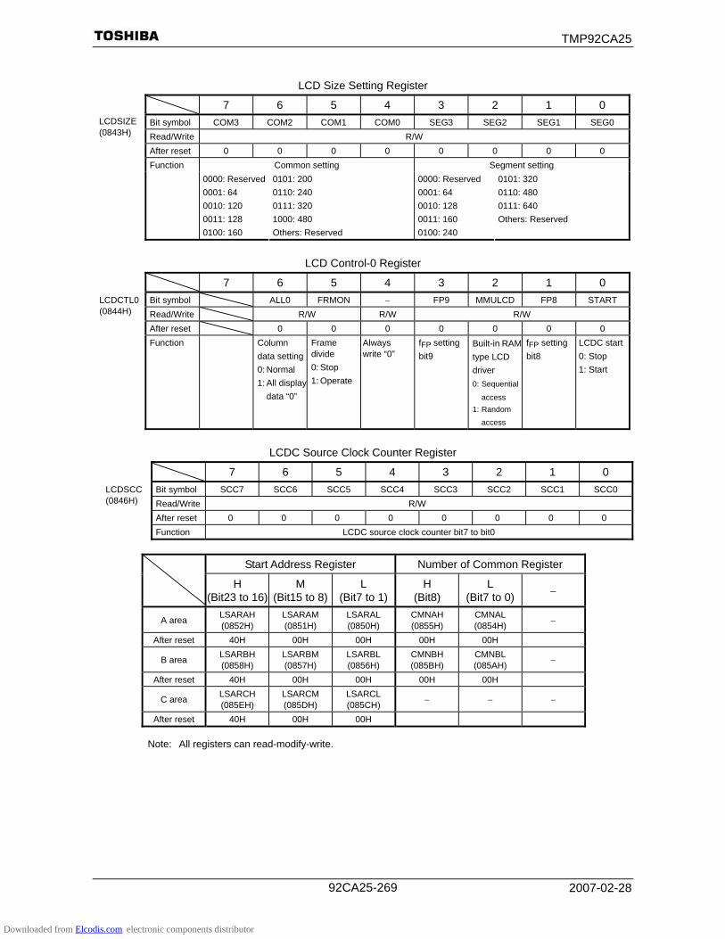
TMP92CA25
2007-02-28 92CA25-269
LCD Size Setting Register
7 6 5 4 3 2 1 0 Bit symbol COM3 COM2 COM1 COM0 SEG3 SEG2 SEG1 SEG0 LCDSIZE
(0843H) Read/Write R/W After reset 0 0 0 0 0 0 0 0
Common setting Segment setting Function 0000: Reserved 0001: 64 0010: 120 0011: 128 0100: 160
0101: 200 0110: 240 0111: 320 1000: 480 Others: Reserved
0000: Reserved 0001: 64 0010: 128 0011: 160 0100: 240
0101: 320 0110: 480 0111: 640 Others: Reserved
LCD Control-0 Register
7 6 5 4 3 2 1 0 Bit symbol ALL0 FRMON − FP9 MMULCD FP8 START LCDCTL0
(0844H) Read/Write R/W R/W R/W After reset 0 0 0 0 0 0 0 Function Column
data setting 0: Normal 1: All display data “0”
Frame divide 0: Stop 1: Operate
Always write “0”
fFP settingbit9
Built-in RAM type LCD driver 0: Sequential
access 1: Random access
fFP setting bit8
LCDC start0: Stop 1: Start
LCDC Source Clock Counter Register
7 6 5 4 3 2 1 0 Bit symbol SCC7 SCC6 SCC5 SCC4 SCC3 SCC2 SCC1 SCC0 LCDSCC
(0846H) Read/Write R/W After reset 0 0 0 0 0 0 0 0 Function LCDC source clock counter bit7 to bit0
Start Address Register Number of Common Register
H (Bit23 to 16)
M (Bit15 to 8)
L (Bit7 to 1)
H (Bit8)
L (Bit7 to 0) −
A area LSARAH (0852H)
LSARAM (0851H)
LSARAL (0850H)
CMNAH (0855H)
CMNAL (0854H) −
After reset 40H 00H 00H 00H 00H
B area LSARBH (0858H)
LSARBM (0857H)
LSARBL (0856H)
CMNBH (085BH)
CMNBL (085AH) −
After reset 40H 00H 00H 00H 00H
C area LSARCH (085EH)
LSARCM (085DH)
LSARCL (085CH) − − −
After reset 40H 00H 00H
Note: All registers can read-modify-write.
Downloaded from Elcodis.com electronic components distributor
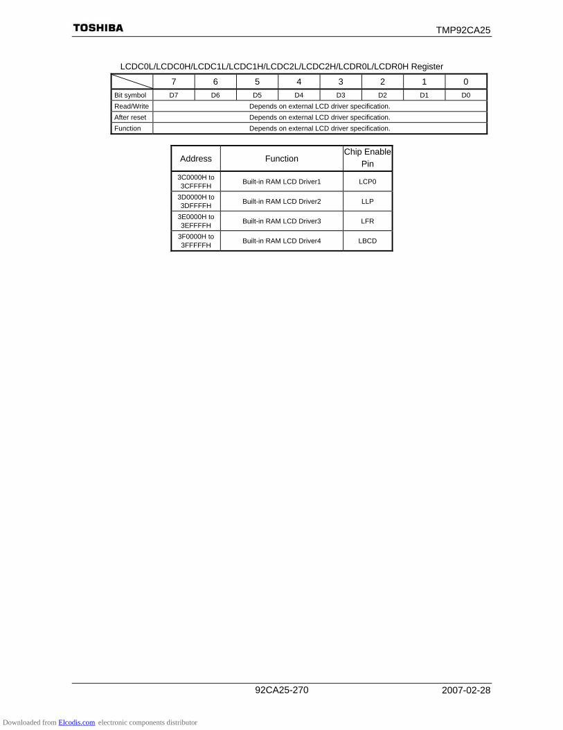
TMP92CA25
2007-02-28 92CA25-270
LCDC0L/LCDC0H/LCDC1L/LCDC1H/LCDC2L/LCDC2H/LCDR0L/LCDR0H Register
7 6 5 4 3 2 1 0 Bit symbol D7 D6 D5 D4 D3 D2 D1 D0 Read/Write Depends on external LCD driver specification.
After reset Depends on external LCD driver specification. Function Depends on external LCD driver specification.
Address Function Chip Enable
Pin 3C0000H to 3CFFFFH Built-in RAM LCD Driver1 LCP0
3D0000H to 3DFFFFH Built-in RAM LCD Driver2 LLP
3E0000H to 3EFFFFH Built-in RAM LCD Driver3 LFR
3F0000H to 3FFFFFH Built-in RAM LCD Driver4 LBCD
Downloaded from Elcodis.com electronic components distributor
TMP92CA25
2007-02-28 92CA25-271
3.15.3 Shift Register Type LCD Driver Control Mode (SR mode)
3.15.3.1 Description of Operation
Set the mode of operation, start address of display memory, grayscale level and LCD size to control registers before setting start register.
After setting start register, the LCDC outputs a bus release request to the CPU and reads data from source memory. After data reading from source data is completed, the LCDC cancels the bus release request and the CPU will restart. The LCDC then transmits LCD size data to the external LCD driver through the LD bus (special data bus only for LCD driver). At this time, the control signals (LCP0 etc.) connected to the LCD driver output the specified waveform which is synchronized with the data transmission.
The LCD controller generates control signals (LFR, LBCD, LLP etc.) from base clock LCDSCC. LCDSCC is the clock generator for the LCD controller, which is generated by system clock fSYS.
This LSI has a special clock generator for the LCDC. Details of LCD frame refresh rate can be set using this special generator. This generator is made from an 8-bit counter and 1/16 speed clock from the system clock.
Note 1: During display data read from source memory (during DMA operation), the CPU is stopped by the internal BUSREQ signal. When using SR mode LCDC, programmers must monitor CPU performance.
Note 2: This LSI has a 16-Kbyte SRAM, this internal RAM is available for use as display RAM. Internal RAM access is very fast (32-bit bus width, 1 SYSCLK read/write), it is possible to reduce CPU load to a minimum. It can also be used 16bits access mode if using internal RAM. This mode is for internal RAM to use as display RAM effectively.
When using display RAM as SDRAM, set SDRAM size by SDACR2 register of
SDRAMC. Data output width is selectable between 4 bits or 8 bits, and data output sequence
selectable between 2 modes. SR type LCD control setting is described below.
Downloaded from Elcodis.com electronic components distributor

TMP92CA25
2007-02-28 92CA25-272
3.15.3.2 Memory Space (Common spec. SR mode and TFT mode)
The LCDC can display an LCD panel image which is divided horizontally into 3 parts; upper, middle and lower. Each area is called A area, B area and C area with the characteristics shown below.
The Start/End address of each area in the physical memory space can be defined in the LCD start/end address registers. C area can be defined only in start address.
A and B areas can be displayed by program and set to enable or not in Start Address register and Row Number register. When the Row Number registers of A and B areas are set to 0, C area takes over all panel space.
When the size of A or B area is greater than the LCD panel, the area of the panel is all C area because the displaying priority is A > B > C. If the A area is set to enable while the panel area is defined as all C area (A and B areas are disabled), C area is shifted below the LCD panel and A area is inserted from the top of the LCD panel. Similarly if the B area is set to enable while the panel area is defined as all C area, B area is inserted from the bottom of the C area overlapping.
Figure 3.15.1 Memory Mapping from Physical Memory to LCD Panel
Logic address 400000H A area
B area
C area
Vertical pan
Column address
Horizontal pan
600000H
Row address
Ya
Yb
Memory map image
LCD Panel image
A area
C area
B area
Ya
Yb
Yc
Reserved area for horizontal pan of C area * Display data cannot input closely when
pan function is not used (SDRAM).
2X
Yc
X
Downloaded from Elcodis.com electronic components distributor
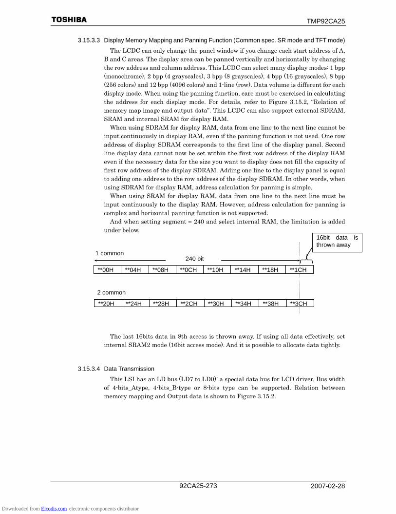
TMP92CA25
2007-02-28 92CA25-273
3.15.3.3 Display Memory Mapping and Panning Function (Common spec. SR mode and TFT mode)
The LCDC can only change the panel window if you change each start address of A, B and C areas. The display area can be panned vertically and horizontally by changing the row address and column address. This LCDC can select many display modes: 1 bpp (monochrome), 2 bpp (4 grayscales), 3 bpp (8 grayscales), 4 bpp (16 grayscales), 8 bpp (256 colors) and 12 bpp (4096 colors) and 1-line (row). Data volume is different for each display mode. When using the panning function, care must be exercised in calculating the address for each display mode. For details, refer to Figure 3.15.2, “Relation of memory map image and output data”. This LCDC can also support external SDRAM, SRAM and internal SRAM for display RAM.
When using SDRAM for display RAM, data from one line to the next line cannot be input continuously in display RAM, even if the panning function is not used. One row address of display SDRAM corresponds to the first line of the display panel. Second line display data cannot now be set within the first row address of the display RAM even if the necessary data for the size you want to display does not fill the capacity of first row address of the display SDRAM. Adding one line to the display panel is equal to adding one address to the row address of the display SDRAM. In other words, when using SDRAM for display RAM, address calculation for panning is simple.
When using SRAM for display RAM, data from one line to the next line must be input continuously to the display RAM. However, address calculation for panning is complex and horizontal panning function is not supported.
And when setting segment = 240 and select internal RAM, the limitation is added under below.
The last 16bits data in 8th access is thrown away. If using all data effectively, set internal SRAM2 mode (16bit access mode). And it is possible to allocate data tightly.
3.15.3.4 Data Transmission
This LSI has an LD bus (LD7 to LD0): a special data bus for LCD driver. Bus width of 4-bits_Atype, 4-bits_B-type or 8-bits type can be supported. Relation between memory mapping and Output data is shown to Figure 3.15.2.
**00H
16bit data is thrown away
**20H **20H
240 bit1 common
2 common
**24H
**04H **08H **0CH **10H **14H **18H **1CH
**28H **2CH **30H **34H **38H **3CH
Downloaded from Elcodis.com electronic components distributor
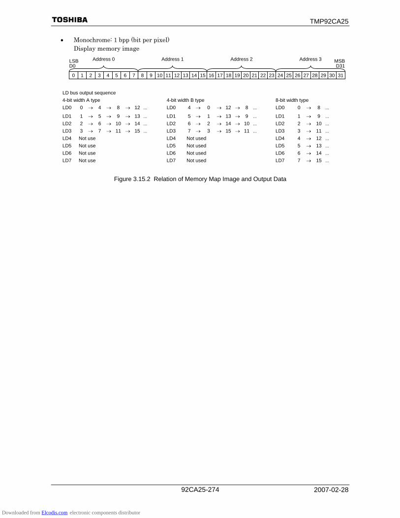
TMP92CA25
2007-02-28 92CA25-274
• Monochrome: 1 bpp (bit per pixel) Display memory image
LD bus output sequence 4-bit width A type 4-bit width B type 8-bit width type LD0 0 → 4 → 8 → 12 ... LD0 4 → 0 → 12 → 8 ... LD0 0 → 8 ...
LD1 1 → 5 → 9 → 13 ... LD1 5 → 1 → 13 → 9 ... LD1 1 → 9 ... LD2 2 → 6 → 10 → 14 ... LD2 6 → 2 → 14 → 10 ... LD2 2 → 10 ... LD3 3 → 7 → 11 → 15 ... LD3 7 → 3 → 15 → 11 ... LD3 3 → 11 ... LD4 Not use LD4 Not used LD4 4 → 12 ... LD5 Not use LD5 Not used LD5 5 → 13 ... LD6 Not use LD6 Not used LD6 6 → 14 ... LD7 Not use LD7 Not used LD7 7 → 15 ...
Figure 3.15.2 Relation of Memory Map Image and Output Data
0 1 2 3 4 5 6 7 8 9 10 11 12 13 14 15 16 17 18 19 20 21 22 23 24 25 26 27 28 29 30 31
Address 0 Address 1 Address 2 Address 3LSB D0
MSBD31
Downloaded from Elcodis.com electronic components distributor

TMP92CA25
2007-02-28 92CA25-275
3.15.3.5 Refresh Rate Setting
Frame cycle (refresh rate) is generated from setting of LSCC (LCDSCC<SCC7:0>) and FP [9:0] (LCDCTL0<FP9, 8>, LCDFFP<FP7:0>). The LBCD terminal outputs one pulse every cycle and the LFR normally outputs an inverted signal every cycle. But when the DIVIDE FRAME function is used, the LFR signal changes to a special signal for high quality display.
(1) Basic clock setting
This LSI has a special clock generator for basic source clock used in the LCD controller. This generator can set details of the refresh rate for the LCDC.
This generator is made by dividing the system clock by 16 and an 8-bit counter. The following shows the method of setting and calculation.
fBCD[Hz]: Frame rate (Refresh rate: Frequency of LBCD signal) FP: FP [9:0] setting value of FFP register SCC: <SCC7:0> setting value of LSCC register fBCD [Hz] = fSYS [Hz] / ((SCC+1) × 16 × FP) Example: fSYS [Hz] = 20MHz, 240COM (FP = 240), target refresh rate = 70Hz 70 [Hz] = 20000000 [Hz]/((SCC+1) × 16 × 240) (SCC+1) = 20000000/(70 ×16 × 240) = 74.4 Value of setting to register is only integer, SCC = 73. The floating value is disregarded. In this case, the refresh rate comes to 70.3 [Hz]
LCDC Source Clock Counter Register
7 6 5 4 3 2 1 0 Bit symbol SCC7 SCC6 SCC5 SCC4 SCC3 SCC2 SCC1 SCC0 LCDSCC
(0846H) Read/Write R/W After reset 0 0 0 0 0 0 0 0 Function LCDC Source Clock Counter bit7 to bit0
* Data should be written from 1-hex to FFFF-hex in the above register. It cancannot operate if set to “0”.
* If the refresh rate is set too fast, it may not be in time with the display data. tLP time is determined by SCC.
tLP [s] = (1/fSYS [Hz]) × 16 × (SCC + 1)
tLP is shown in 1-line (ROW) display time. 1-line data transmission must be completed during tLP cycle time. AboutRefer to “Data transmission and bus occupation” for details of data transmission time.
Downloaded from Elcodis.com electronic components distributor
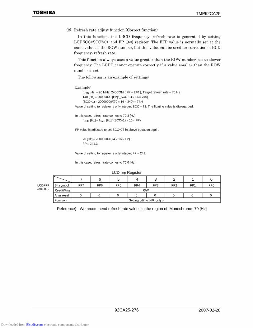
TMP92CA25
2007-02-28 92CA25-276
(2) Refresh rate adjust function (Correct function)
In this function, the LBCD frequency: refresh rate is generated by setting LCDSCC<SCC7:0> and FP [9:0] register. The FFP value is normally set at the same value as the ROW number, but this value can be used for correction of BCD frequency: refresh rate.
This function always uses a value greater than the ROW number, set to slower frequency. The LCDC cannot operate correctly if a value smaller than the ROW number is set.
The following is an example of settings:
Example: fSYS [Hz] = 20 MHz, 240COM ( FP = 240 ), Target refresh rate = 70 Hz 140 [Hz] = 20000000 [Hz]/((SCC+1) × 16 × 240) (SCC+1) = 20000000/(70 × 16 × 240) = 74.4 Value of setting to register is only integer, SCC = 73. The floating value is disregarded.
In this case, refresh rate comes to 70.3 [Hz] fBCD [Hz] = fSYS [Hz]/((SCC+1) × 16 × FP) FP value is adjusted to set SCC=73 in above equation again. 70 [Hz] = 20000000/(74 × 16 × FP) FP = 241.3 Value of setting to register is only integer, FP = 241.
In this case, refresh rate comes to 70.0 [Hz]
LCD fFP Register
7 6 5 4 3 2 1 0 Bit symbol FP7 FP6 FP5 FP4 FP3 FP2 FP1 FP0 LCDFFP
(0841H) Read/Write R/W After reset 0 0 0 0 0 0 0 0 Function Setting bit7 to bit0 for fFP
Reference) We recommend refresh rate values in the region of: Monochrome: 70 [Hz]
Downloaded from Elcodis.com electronic components distributor

TMP92CA25
2007-02-28 92CA25-277
(3) Divide frame adjust function
The DIVIDE FRAME function allows for adjustments to reduce uneven display in large LCD panels.
When this function is enabled by setting <FRMON> = 1, the LFR signal alternates between high and low level with each LLP cycle for the LCDDVM register values given below.
When this function is disabled by setting LCDCTL<FRMON> = 0, the LFR signal alternates between high and low level with each LBCD cycle. This function is not affected by the LBCD timing.
Note: Availability of this function depends on the actual LCD driver or LCD panel used. We recommend checking that register’s value when used in the proposed environment.
Divide Frame Register
7 6 5 4 3 2 1 0 Bit symbol FMN7 FMN6 FMN5 FMN4 FMN3 FMN2 FMN1 FMN0 LCDDVM
(0842H) Read/Write R/W After reset 0 0 0 0 0 0 0 0 Function Setting DVM bit7 to bit0
(Reference) In general, prime numbers (3, 5, 7, 11, 13 ...) are best for the value of the LCDDVM register.
Downloaded from Elcodis.com electronic components distributor

TMP92CA25
2007-02-28 92CA25-278
Figure 3.15.3 Whole Timing Diagram of SR Mode
Note: There is internal FI/FO_RAM (160bits) for controlling the speed of transfering to LCD driver. If the size of
segment is over 160, several bus request is generated at one tLP interval. (640segment: 5times max)
Figure 3.15.4 Detailed Timing Diagram of SR Mode
Condition: FFP [9:0] setting = 240 (COM) + 63, LCDDVM<FMN7:0> = 0BH
Figure 3.15.5 Waveform of LLP, LFR
LFR
LBCD
LLP
LCP
LD7 to LD0 (8-bit case)
1 2 3 1 2 3 1 2120 120
Use internal signal to CPU (Interrupt)
LFR
LBCD
LLP Use internal signal
(Internal) BUSRQ
LCP0
LD7 to LD0 (8 bits) N N + 1 N + 28 N + 29
tLP: LLP cycle
tSTOP: Stop time tOPR: CPU opration time
tCP = 2 states
tLPH = fSYS × 4
LLP
LFR
LP1 LP2 LP3 LP10 LP11 LP301 LP302 LP303 LP304
DVM disable
DVM enable
Downloaded from Elcodis.com electronic components distributor

TMP92CA25
2007-02-28 92CA25-279
3.15.3.6 LCD Data Transmission Speed and Data Bus Occupation Rate
After setting start register, the LCDC outputs a bus release request to the CPU and reads data from source memory. The LCDC then transmits LCD size data to the external LCD driver through the special LCDC data bus (LD11 to LD0). At this time, the control signals connected to the LCD driver output the specified waveform which is synchronized with the data transmission. After data reading from RAM for display is completed, the LCDC cancels the bus release request and the CPU will restart.
During data read from source memory (during DMA operation), the CPU is stopped by the internal BUSREQ signal. When using SR mode LCDC, programmers must monitor CPU performance. The occupation rate of the data bus depends on data size, transmission speed (CPU clock speed) and display RAM type used.
Display RAM Bus Width Valid Data Reading Time
(fSYS Clock/Byte)
Valid Data Reading TimetLRD (ns/Byte)
at fSYS = 20 MHz 16 bits 2/2 50
External SRAM 32 bits 2/4 25
Internal RAM 32 bits 1/4 12.5 External SDRAM 16 bits *1/2 *25
Note: When using SDRAM for display RAM, overhead time (+ 8 clocks) is required for every 1 row data reading.
tSTOP refers to the CPU stoppage time during transmission of 1 row data. tSTOP
is calculated by the equation below for each display mode.
tSTOP = (SegNum /8) × tLRD SegNum : Number of segment When SDRAM is used, more overhead time is required. tSTOP = (SegNum /8) × tLRD + ((1/fSYS) × 8)
Data bus occupation rate equals the percentage of tSTOP time in tLP time.
Data bus occupation rate = tSTOP/tLP Note: For tLP time, refer to “refresh rate setting”.
Downloaded from Elcodis.com electronic components distributor
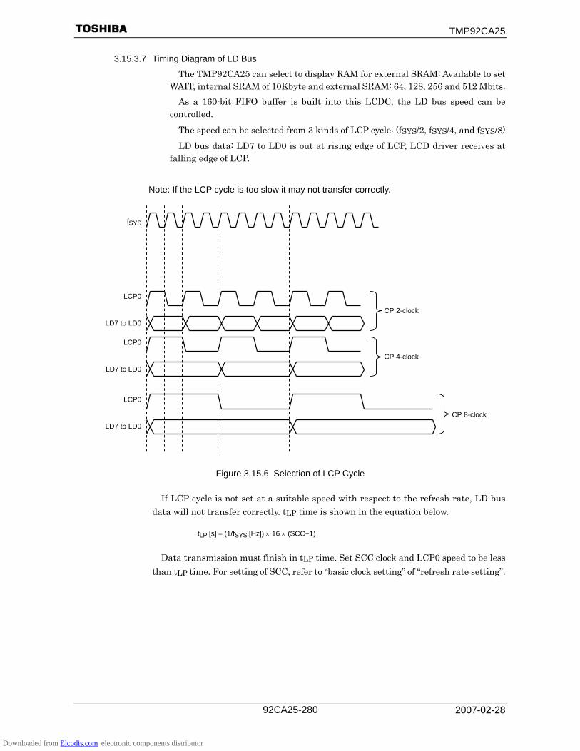
TMP92CA25
2007-02-28 92CA25-280
3.15.3.7 Timing Diagram of LD Bus
The TMP92CA25 can select to display RAM for external SRAM: Available to set WAIT, internal SRAM of 10Kbyte and external SRAM: 64, 128, 256 and 512 Mbits.
As a 160-bit FIFO buffer is built into this LCDC, the LD bus speed can be controlled.
The speed can be selected from 3 kinds of LCP cycle: (fSYS/2, fSYS/4, and fSYS/8) LD bus data: LD7 to LD0 is out at rising edge of LCP, LCD driver receives at
falling edge of LCP.
Note: If the LCP cycle is too slow it may not transfer correctly.
Figure 3.15.6 Selection of LCP Cycle
If LCP cycle is not set at a suitable speed with respect to the refresh rate, LD bus data will not transfer correctly. tLP time is shown in the equation below.
tLP [s] = (1/fSYS [Hz]) × 16 × (SCC+1)
Data transmission must finish in tLP time. Set SCC clock and LCP0 speed to be less
than tLP time. For setting of SCC, refer to “basic clock setting” of “refresh rate setting”.
fSYS
LCP0
LD7 to LD0
CP 2-clock
LCP0
LD7 to LD0
LCP0
LD7 to LD0
CP 4-clock
CP 8-clock
Downloaded from Elcodis.com electronic components distributor
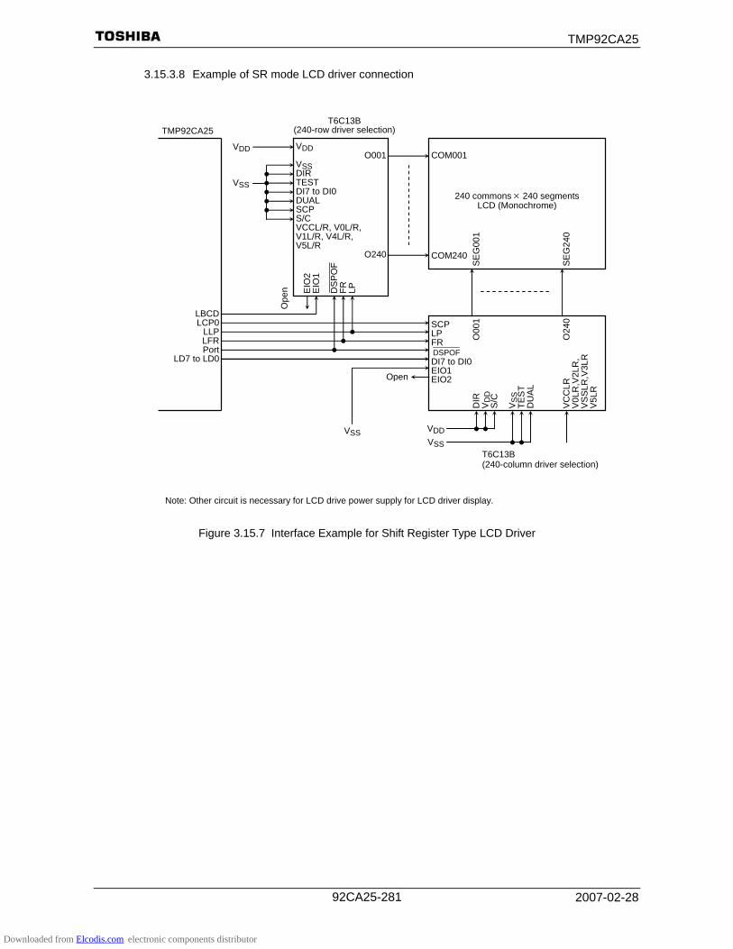
TMP92CA25
2007-02-28 92CA25-281
3.15.3.8 Example of SR mode LCD driver connection
Note: Other circuit is necessary for LCD drive power supply for LCD driver display.
Figure 3.15.7 Interface Example for Shift Register Type LCD Driver
TMP92CA25
VDD
VSS
VDD O001
VSS DIR TEST DI7 to DI0 DUAL SCP S/C VCCL/R, V0L/R, V1L/R, V4L/R, V5L/R
O240
EIO
2 E
IO1
DS
PO
F FR
LP
Ope
n
VSS
LBCD LCP0
LLP LFR Port
LD7 to LD0
SCP LP FR DSPOF DI7 to DI0 EIO1 EIO2
DIR
V
DD
S
/C
VS
S
TES
T D
UA
L V
CC
LR
V0L
R,V
2LR
, V
SS
LR,V
3LR
V
5LR
O00
1
O24
0
Open
VDDVSS
COM001 COM240
SE
G00
1 S
EG
240
240 commons × 240 segments LCD (Monochrome)
T6C13B (240-row driver selection)
T6C13B (240-column driver selection)
Downloaded from Elcodis.com electronic components distributor
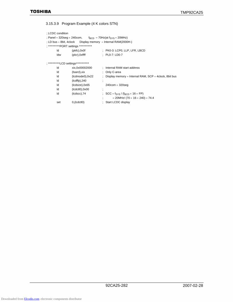
TMP92CA25
2007-02-28 92CA25-282
3.15.3.9 Program Example (4 K colors STN)
; LCDC condition ; Panel = 320seg × 240com, fBCD = 70Hz(at fSYS = 20MHz) ; LD bus = 8bit, 4clock Display memory = Internal RAM(2000H-) ; ********PORT settings ********* ld (pkfc),0x0f ; PK0-3: LCP0, LLP, LFR, LBCD ldw (plcr),0xffff ; PL0-7: LD0-7 ; ********LCD settings********* ld xix,0x00002000 ; Internal RAM start address ld (lsarcl),xix ; Only C-area ld (lcdmode0),0x22 ; Display memory = Internal RAM, SCP = 4clock, 8bit bus ld (lcdffp),240 ; ld (lcdsize),0x65 240com × 320seg ld (lcdctl0),0x00 ; ld (lcdscc),74 ; SCC = fSYS / (fBCD × 16 × FP) ; = 20MHz/ (70 × 16 × 240) = 74.4 set 0,(lcdctl0) ; Start LCDC display
Downloaded from Elcodis.com electronic components distributor
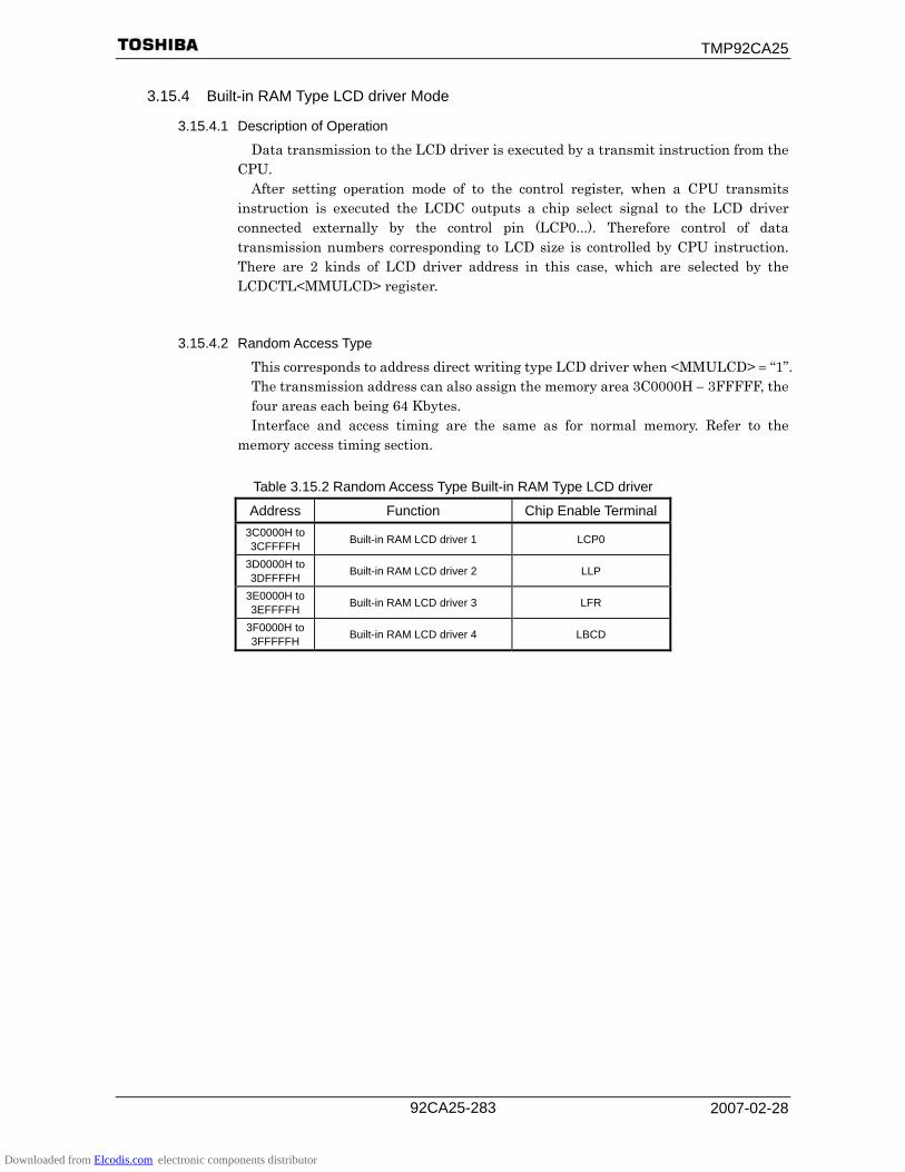
TMP92CA25
2007-02-28 92CA25-283
3.15.4 Built-in RAM Type LCD driver Mode
3.15.4.1 Description of Operation
Data transmission to the LCD driver is executed by a transmit instruction from the CPU.
After setting operation mode of to the control register, when a CPU transmits instruction is executed the LCDC outputs a chip select signal to the LCD driver connected externally by the control pin (LCP0...). Therefore control of data transmission numbers corresponding to LCD size is controlled by CPU instruction. There are 2 kinds of LCD driver address in this case, which are selected by the LCDCTL<MMULCD> register.
3.15.4.2 Random Access Type
This corresponds to address direct writing type LCD driver when <MMULCD> = “1”. The transmission address can also assign the memory area 3C0000H − 3FFFFF, the four areas each being 64 Kbytes. Interface and access timing are the same as for normal memory. Refer to the
memory access timing section.
Table 3.15.2 Random Access Type Built-in RAM Type LCD driver
Address Function Chip Enable Terminal 3C0000H to 3CFFFFH Built-in RAM LCD driver 1 LCP0
3D0000H to 3DFFFFH Built-in RAM LCD driver 2 LLP
3E0000H to 3EFFFFH Built-in RAM LCD driver 3 LFR
3F0000H to 3FFFFFH Built-in RAM LCD driver 4 LBCD
Downloaded from Elcodis.com electronic components distributor

TMP92CA25
2007-02-28 92CA25-284
3.15.4.3 Sequential Access Type
Data transmission to the LCD driver is executed by a transmit instruction from the CPU.
After setting operation mode to the control register, when a CPU transmit instruction is executed the LCDC outputs a chip select signal to the LCD driver connected externally by the control pin (LCP0...). Therefore control of data transmission numbers corresponding to LCD size is controlled by CPU instruction . There are 2 kinds of LCD driver address in this case, which are selected by the LCDCTL<MMULCD> register.
This corresponds to a LCD driver which has each 1 byte of instruction register and display data register in LCD driver when <MMULCD> = “0”. Please select the transmission address at this time from 1FE0H to 1FE7H.
LCDC0L/LCDC0H/LCDC1L/LCDC1H/LCDC2L/LCDC2H/LCDR0L/LCDR0H Register
7 6 5 4 3 2 1 0 Bit symbol D7 D6 D5 D4 D3 D2 D1 D0 Read/Write Depends on external LCDD specification
After reset Depends on external LCDD specification Function Depends on external LCDD specification
Note 1: This waveform is in the case of 3-state access.
Note 2: Rising timing of chip enable signal (e.g LCP0) is different.
Figure 3.15.8 Example of Access Timing for Built-in RAM Type LCD Driver (Wait = 0)
WAIT sampling
D7 to D0
LCP0, LLP,LFR, LBCD
R/ W
A23 to A0
System clock: fSYS
Data out
T1 TW T2
[Write cycle]
Data in
T1 TW T2
[Read cycle]
Downloaded from Elcodis.com electronic components distributor
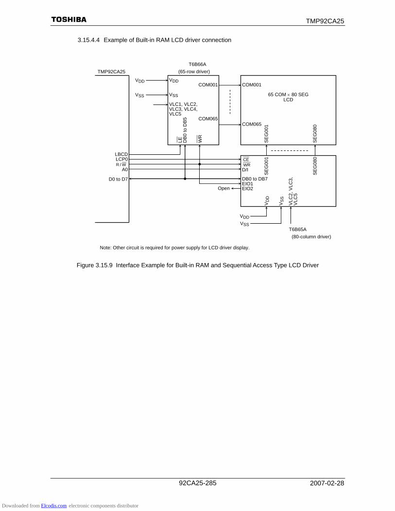
TMP92CA25
2007-02-28 92CA25-285
3.15.4.4 Example of Built-in RAM LCD driver connection
Note: Other circuit is required for power supply for LCD driver display.
Figure 3.15.9 Interface Example for Built-in RAM and Sequential Access Type LCD Driver
TMP92CA25
VDD
VSS
VDD COM001
VSS VLC1, VLC2, VLC3, VLC4, VLC5
COM065
LE
DB
0 to
DB
5 W
R
LBCDLCP0
W/RA0
D0 to D7
CE WR D/I DB0 to DB7 EIO1 EIO2
VD
D
VS
S
VLC
2, V
LC3,
V
LC5
SE
G00
1
SE
G08
0
Open
VDDVSS
COM001 COM065
SE
G00
1 S
EG
080
65 COM × 80 SEG LCD
T6B66A (65-row driver)
T6B65A (80-column driver)
Downloaded from Elcodis.com electronic components distributor
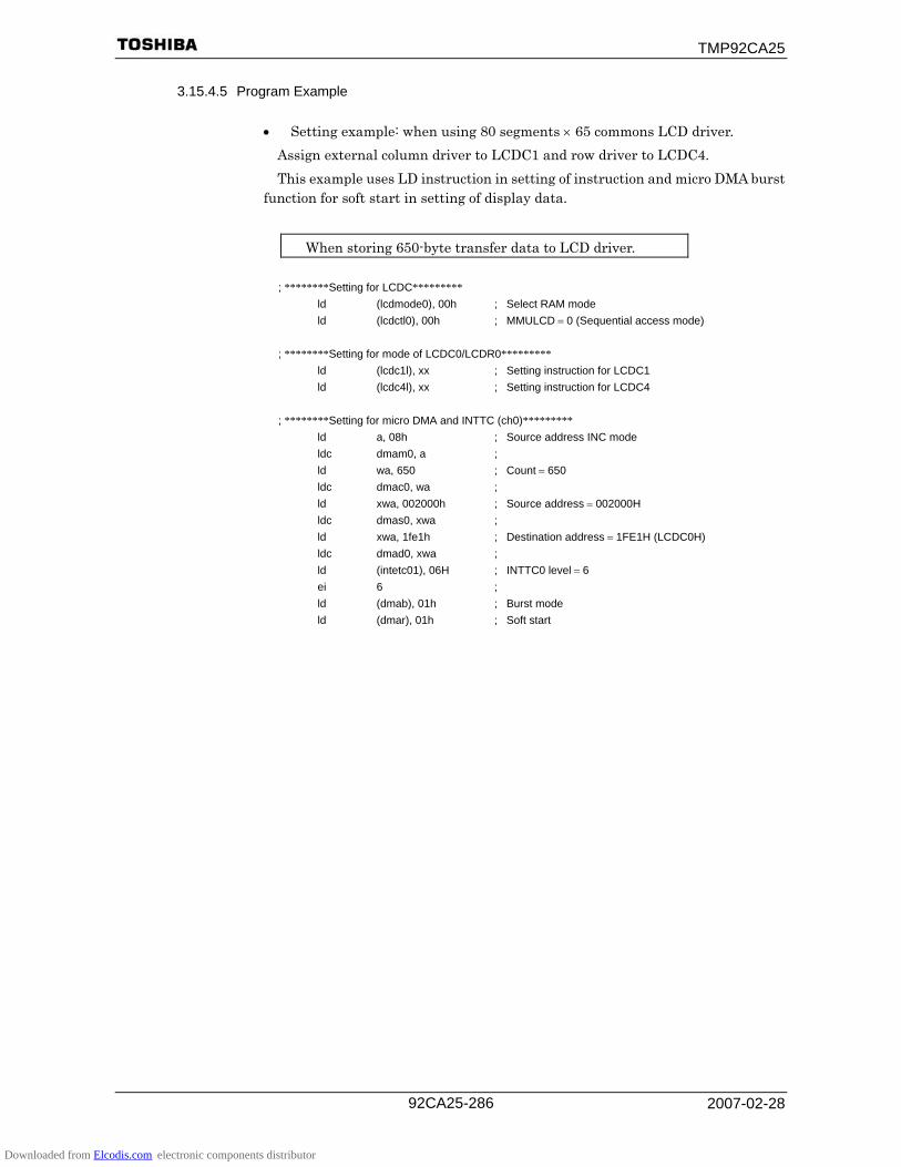
TMP92CA25
2007-02-28 92CA25-286
3.15.4.5 Program Example
• Setting example: when using 80 segments × 65 commons LCD driver. Assign external column driver to LCDC1 and row driver to LCDC4. This example uses LD instruction in setting of instruction and micro DMA burst
function for soft start in setting of display data.
When storing 650-byte transfer data to LCD driver.
; ********Setting for LCDC********* ld (lcdmode0), 00h ; Select RAM mode ld (lcdctl0), 00h ; MMULCD = 0 (Sequential access mode) ; ********Setting for mode of LCDC0/LCDR0********* ld (lcdc1l), xx ; Setting instruction for LCDC1 ld (lcdc4l), xx ; Setting instruction for LCDC4 ; ********Setting for micro DMA and INTTC (ch0)********* ld a, 08h ; Source address INC mode ldc dmam0, a ; ld wa, 650 ; Count = 650 ldc dmac0, wa ; ld xwa, 002000h ; Source address = 002000H ldc dmas0, xwa ; ld xwa, 1fe1h ; Destination address = 1FE1H (LCDC0H) ldc dmad0, xwa ; ld (intetc01), 06H ; INTTC0 level = 6 ei 6 ; ld (dmab), 01h ; Burst mode ld (dmar), 01h ; Soft start
Downloaded from Elcodis.com electronic components distributor
TMP92CA25
2007-02-28 92CA25-287
3.16 Melody/Alarm Generator (MLD)
The TMP92CA25 contains a melody function and alarm function, both of which are output from the MLDALM pin. Five kinds of fixed cycle interrupt are generated using a 15-bit counter for use as the alarm generator.
The features are as follows.
1) Melody generator The Melody function generates signals of any frequency (4 Hz to 5461 Hz) based on a
low-speed clock (32.768 kHz), and outputs the signals from the MLDALM pin. The melody tone can easily be heard by connecting an external loudspeaker.
2) Alarm generator
The alarm function generates eight kinds of alarm waveform having a modulation frequency (4096 Hz) determined by the low-speed clock (32.768 kHz). This waveform can be inverted by setting a value to a register.
The alarm tone can easily be heard by connecting an external loudspeaker. Five kinds of fixed cycle interrupts are generated (1 Hz, 2 Hz, 64 Hz, 512 Hz, and 8192
Hz) by using a counter which is used for the alarm generator. This section is constituted as follows. 3.16.1 Block Diagram 3.16.2 Control Registers 3.16.3 Operational description 3.16.3.1 Melody Generator 3.16.3.2 Alarm Generator
Downloaded from Elcodis.com electronic components distributor

TMP92CA25
2007-02-28 92CA25-288
3.16.1 Block Diagram
Figure 3.16.1 MLD Block Diagram
MELFH, MELFL register
Comparator (CP0)
12-bit counter (UC0)
F/F
[Melody Generator]
Edgedetector
ALMINT<IALM4E:0E>
15-bit counter (UC1)
8-bit counter (UC2)
Alarm wave form generator
ALM register
Invert
MELALMC<ALMINV>
Selector
ALMOUT
MELOUT
MELALMC<FC1:0>
Internal data busReset
MELFH <MELON>
Stop and clear
Low-speed clock
InvertMELOUT
[Alarm Generator] Internal data busReset
INTALM0 (8192 Hz)
INTALM1 (512 Hz)
INTALM2 (64 Hz)
INTALM3 (2 Hz)
INTALM4 (1 Hz)
INTALMH(HALT release)
MLDALM pin
4096 Hz
Clear
MELALMC <MELALM>
Downloaded from Elcodis.com electronic components distributor

TMP92CA25
2007-02-28 92CA25-289
3.16.2 Control Registers
ALM Register
7 6 5 4 3 2 1 0 Bit symbol AL8 AL7 AL6 AL5 AL4 AL3 AL2 AL1 ALM
(1330H) Read/Write R/W After reset 0 0 0 0 0 0 0 0 Function Setting alarm pattern
MELALMC Register
7 6 5 4 3 2 1 0 Bit symbol FC1 FC0 ALMINV − − − − MELALMMELALMC
(1331H) Read/Write R/W After reset 0 0 0 0 0 0 0 0 Function Free-run counter control
00: Hold 01: Restart 10: Clear 11: Clear and start
Alarm waveform invert 1: Invert
Always write “0”
Output waveform select 0: Alarm 1: Melody
Note 1: MELALMC<FC1> is always read “0”.
Note 2: When setting MELALMC register except <FC1:0> while the free-run counter is running, <FC1:0> is kept
“01”.
MELFL Register
7 6 5 4 3 2 1 0 Bit symbol ML7 ML6 ML5 ML4 ML3 ML2 ML1 ML0 MELFL
(1332H) Read/Write R/W After reset 0 0 0 0 0 0 0 0 Function Setting melody frequency (Lower 8 bits)
MELFH Register
7 6 5 4 3 2 1 0 Bit symbol MELON ML11 ML10 ML9 ML8 MELFH
(1333H) Read/Write R/W R/W After reset 0 0 0 0 0 Function Control
melody counter 0: Stop and
clear 1: Start
Setting melody frequency (Upper 4 bits)
ALMINT Register
7 6 5 4 3 2 1 0 Bit symbol − IALM4E IALM3E IALM2E IALM1E IALM0E ALMINT
(1334H) Read/Write R/W After reset 0 0 0 0 0 0 Function Always
write “0” 1: Interrupt enable for INTALM4 to INTALM0
Downloaded from Elcodis.com electronic components distributor
TMP92CA25
2007-02-28 92CA25-290
3.16.3 Operational description
3.16.3.1 Melody Generator
The Melody function generates signals of any frequency (4 Hz to 5461 Hz) based on a low-speed clock (32.768 kHz) and outputs the signals from the MLDALM pin.
The melody tone can easily be heard by connecting an external loud speaker.
(Operation) MELALMC<MELALM> must first be set as 1 in order to select the melody
waveform to be output from MLDALM. The melody output frequency must then be set to 12-bit registers MELFH and MELFL.
The following are examples of settings and calculations of melody output frequency.
(Formula for calculating melody waveform frequency)
at fs = 32.768 [kHz] Melody output waveform fMLD [Hz] = 32768/(2 × N + 4) Setting value for melody N = (16384/ fMLD) − 2 (Note: N = 1 to 4095 (001H to FFFH), 0 is not acceptable.)
(Example program)
When outputting an “A” musical note (440 Hz) LD (MELALMC), − − X X X X X 1 B ; Select melody waveform LD (MELFL), 23H ; N = 16384/440 − 2 = 35.2 = 023H LD (MELFH), 80H ; Start to generate waveform
Reference) Basic musical scale setting table
Scale Frequency [Hz] Register Value: N C 264 03CH D 297 035H E 330 030H F 352 02DH G 396 027H A 440 023H B 495 01FH C 528 01DH
Downloaded from Elcodis.com electronic components distributor

TMP92CA25
2007-02-28 92CA25-291
3.16.3.2 Alarm Generator
The alarm function generates eight kinds of alarm waveform having a modulation frequency of 4096 Hz determined by the low-speed clock (32.768 kHz). This waveform is reversible by setting a value to a register.
The alarm tone can easily be heard by connecting an external loud speaker . Five kinds of fixed cycle (interrupts can be generated 1 Hz, 2 Hz, 64 Hz, 512 Hz, 8
192 Hz) by using a counter which is used for the alarm generator.
(Operation) MELALMC<MELALM> must first be set as 0 in order to select the alarm
waveform to be output from MLDALMC. The “10” must be set on the MELALMC <FC1:0> register, and clear internal counter.
Finally the alarm pattern must then be set on the 8-bit register of ALM. If it is inverted output-data, set <ALMINV> as invert.
The following are examples of program, setting value of alarm pattern and waveform of each setting value.
(Setting value of alarm pattern)
Setting Value for ALM Register Alarm Waveform 00H Write “0” 01H AL1 pattern 02H AL2 pattern 04H AL3 pattern 08H AL4 pattern 10H AL5 pattern 20H AL6 pattern 40H AL7 pattern 80H AL8 pattern
Others Undefined (Do not set)
(Example program)
When outputting AL2 pattern (31.25 ms/8 times/1 s) LD (MELALMC), C0H ; Set output alarm waveform ; Free-run counter start LD (ALM), 02H ; Set AL2 pattern, start
Downloaded from Elcodis.com electronic components distributor

TMP92CA25
2007-02-28 92CA25-292
Example: Waveform of alarm pattern for each setting value (Not inverted)
500 ms
1 AL3 pattern (Once)
250 ms
AL8 pattern (Once)
Modulation frequency(4096 Hz)
AL1 pattern (Continuous output)
31.25 ms 1 s
1 2 8 1 AL2 pattern (8 times/1 s)
62.5 ms 1 s
1 2 1 AL4 pattern (Twice/1 s)
62.5 ms 1 s
1 2 1 3AL5 pattern (3 times/1 s)
62.5 ms
1 AL6 pattern (Once)
62.5 ms
1 2 AL7 pattern (Twice)
Downloaded from Elcodis.com electronic components distributor
TMP92CA25
2007-02-28 92CA25-293
3.17 SDRAM Controller (SDRAMC)
The TMP92CA25 includes an SDRAM controller which supports SDRAM access by CPU/LCDC.
The features are as follows.
(1) Support SDRAM Data rate type: Only SDR (Single data rate) type Bulk of memory: 16/64/128/256/512 Mbits Number of banks: 2/4 banks Width of data bus: 16 Read burst length: 1 word/full page Write mode: Single/burst
(2) Initialize function
All banks precharge command 8 times auto refresh command Set the mode register command
(3) Access mode
CPU Access LCDC Access Read burst length 1 word/full page selectable Full page Addressing mode Sequential Sequential CAS latency (clock) 2 2 Write mode Single/burst selectable −
(4) Access cycle CPU Access (Read/write) Read cycle: 1 word− 4 states/full page − 1 state Write cycle: Single − 3 states/burst − 1 state Access data width: 1 byte/ 1 word/ 1 long word LCDC Burst Access (Read only) Read cycle: full page − 1 state Full page Over head: 4 states (200 ns at fSYS = 20 MHz) Access data width: 1 word/ 1 long word
(5) Refresh cycle auto generate
Auto-refresh is generated while another area is being accessed. Refresh interval is programmable. Self-refresh is supported
Note 1: Display data for LCDC must be set from the head of each page.
Note 2: Condition of SDRAM’s area set by CS1 setting of memory controller.
Downloaded from Elcodis.com electronic components distributor

TMP92CA25
2007-02-28 92CA25-294
3.17.1 Control Registers
Figure 3.17.1 shows the SDRAMC control registers. Setting these registers controls the operation of SDRAMC.
SDRAM Access Control Register 1
7 6 5 4 3 2 1 0 Bit symbol − − SMRD SWRC SBST SBL1 SBL0 SMAC SDACR1
(0250H) Read/Write R/W After reset 0 0 0 0 0 1 0 0 Function Always
write “0” Always write “0”
Mode register set delay time0: 1 clock 1: 2 clocks
Write recover time 0: 1 clock 1: 2 clocks
Burst stop command 0: Precharge
all
1: Burst stop
Selecting burst length (Note 1) 00: Reserved 01: Full-page read, burst
write 10: 1-word read, single
write 11: Full-page read, single
write
SDRAM controller 0: Disable1: Enable
Note 1: Issue mode register set command after changing <SBL1:0>. Exercise care in settings when changing from
“full-page read” to “1-word read”. Please refer to “Limitations arising when using SDRAM”.
SDRAM Access Control Register 2
7 6 5 4 3 2 1 0 Bit symbol SBS SDRS1 SDRS0 SMUXW1 SMUXW0SDACR2
(0251H) Read/Write R/W After reset 0 0 0 0 0 Function Number of
banks 0: 2 banks1: 4 banks
Selecting ROW address size 00: 2048 rows (11 bits) 01: 4096 rows (12 bits) 10: 8192 rows (13 bits) 11: Reserved
Selecting address multiplex type 00: TypeA (A9-) 01: TypeB (A10-) 10: TypeC (A11-) 11: Reserved
SDRAM Refresh Control Register
7 6 5 4 3 2 1 0 Bit symbol − SSAE SRS2 SRS1 SRS0 SRC SDRCR
(0252H) Read/Write R/W R/W After reset 0 1 0 0 0 0 Function Always
write “0” SR Auto
Exit function 0: Disable 1: Enable
Refresh interval 000: 47 states 100: 156 states 001: 78 states 101: 195 states 010: 97 states 110: 249 states 011: 124 states 111: 312 states
Auto refresh 0: Disable1: Enable
Downloaded from Elcodis.com electronic components distributor

TMP92CA25
2007-02-28 92CA25-295
SDRAM Command Register
7 6 5 4 3 2 1 0 Bit symbol SCMM2 SCMM1 SCMM0 SDCMM
(0253H) Read/Write R/W After reset 0 0 0 Function Command issue
(Note 1) (Note 2) 000: Not execute 001: Initialization sequence
a. Precharge All command b. Eight Auto Refresh commands c. Mode Register Set command
100: Mode Register Set command 101: Self Refresh Entry command 110: Self Refresh Exit command Others: Reserved
Note 1: <SCMM2:0> is automatically cleared to “000” after the specified command is issued. Before writing the next
command, make sure that <SCMM2:0> is “000”. In the case of the Self Refresh Entry command, however,
<SCMM2:0> is not cleared to “000” by execution of this command. Thus, this register can be used as a flag
for checking whether or not Self Refresh is being performed.
Note 2: The Self Refresh Exit command can only be specified while Self Refresh is being performed.
Figure 3.17.1 SDRAM Control Registers
Downloaded from Elcodis.com electronic components distributor

TMP92CA25
2007-02-28 92CA25-296
3.17.2 Operation Description
(1) Memory access control SDRAM controller is enabled when SDACR1<SMAC> = 1. And then SDRAM control
signals ( SDCS , SDRAS , SDCAS , SDWE , SDLLDQM, SDLUDQM, SDCLK and SDCKE) are operating during the time CPU or LCDC accesses CS1 area.
1. Address multiplex function
In the access cycle, outputs row/column address through A0 to A15 pin. And multiplex width is decided by setting SDACR2<SMUXW0:1> of use memory size. The relation between multiplex width and Row/Column address is shown in Table 3.17.1 Address Multiplex.
Table 3.17.1 Address Multiplex
Address of SDRAM Accessing Cycle
Row Address Column Address TMP92CA25 Pin Name TypeA
<SMUXW> “00” TypeB
<SMUXW> “01”TypeC
<SMUXW> “10”16-Bit Data Bus Width
B1CSH<BnBUS> = “01” 32-Bit Data Bus Width
B1CSH<BnBUS> = “10”A0 A9 A10 A11 A1 A2 A1 A10 A11 A12 A2 A3 A2 A11 A12 A13 A3 A4 A3 A12 A13 A14 A4 A5 A4 A13 A14 A15 A5 A6 A5 A14 A15 A16 A6 A7 A6 A15 A16 A17 A7 A8 A7 A16 A17 A18 A8 A9 A8 A17 A18 A19 A9 A10 A9 A18 A19 A20 A10 A11
A10 A19 A20 A21 AP * AP * A11 A20 A21 A22 A12 A21 A22 A23 A13 A22 A23 EA24 A14 A23 EA24 EA25 A15 EA24 EA25 EA26
Row address
* AP: Auto Precharge
Burst length of SDRAM read/write by CPU can be select by setting SDACR1<SBL1:0>. Burst length of accessing by LCDC is fixed to operation contents.
SDRAM access cycle is shown in Figure 3.17.2 and Figure 3.17.3. SDRAM access cycle number does not depend on the settings of B1CSL register. In
the full page burst read cycle, a mode register set cycle and a precharge cycle are automatically inserted at the beginning and end of a cycle.
(2) Instruction executing on SDRAM
The CPU can execute instructions on SDRAM. However, the following functions do not operate.
a) Executing HALT instruction b) Execute instructions that write to SDCMM register
These operations must be executed by another memory such as the built-in RAM.
Downloaded from Elcodis.com electronic components distributor
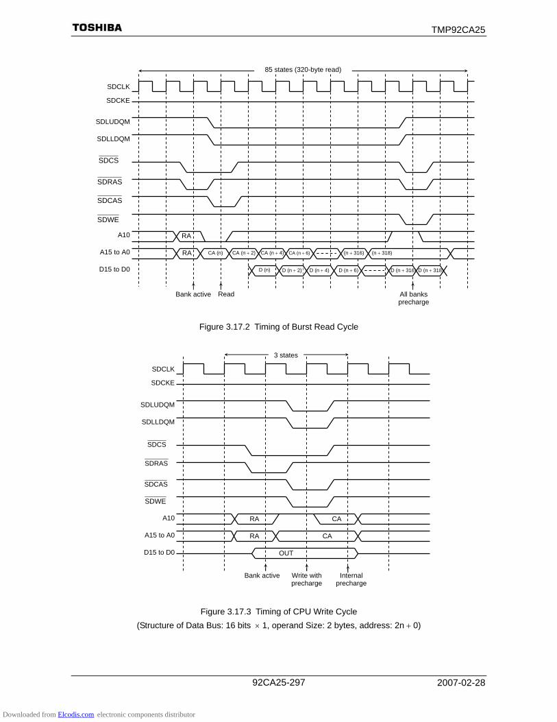
TMP92CA25
2007-02-28 92CA25-297
Figure 3.17.2 Timing of Burst Read Cycle
Figure 3.17.3 Timing of CPU Write Cycle (Structure of Data Bus: 16 bits × 1, operand Size: 2 bytes, address: 2n + 0)
SDCS
Read
(n + 318) (n + 316)CA (n + 6)CA (n + 4)CA (n + 2)
D (n + 4) D (n + 6) D (n + 316) D (n + 318) D (n + 2)
RA
SDCLK
SDCKE
SDLUDQM
SDLLDQM
A10 RA
A15 to A0
D (n)D15 to D0
Bank active All banks precharge
85 states (320-byte read)
CA (n)
SDRAS
SDCAS
SDWE
3 states
SDCLK
SDCKE
SDLUDQM
SDLLDQM
A10 RA
A15 to A0
D15 to D0
Bank active Internal precharge
CA
Write with precharge
RA CA
OUT
SDCS
SDRAS
SDCAS
SDWE
Downloaded from Elcodis.com electronic components distributor

TMP92CA25
2007-02-28 92CA25-298
(3) Refresh control
This LSI supports two refresh commands: auto-refresh and self-refresh.
(a) Auto-refresh The auto-refresh command is automatically generated at intervals set by
SDRCR<SRS2:0> by setting SDRCR<SRC> to “1”. The generation interval can be set from between 47 to 312 states (2.4 μs to 15.6 μs at fSYS = 20 MHz).
CPU operation (instruction fetch and execution) stops while performing the auto-refresh command. The auto-refresh cycle is shown in Figure 3.17.4 and the auto-refresh generation interval is shown in Table 3.17.2. The Auto-Refresh function cannot be used in IDLE1 and STOP modes. In these modes, use the Self- Refresh function to be explained next.
Note: A system reset disables the Auto-Refresh function.
Figure 3.17.4 Timing of Auto-Refresh Cycle
Table 3.17.2 Refresh Cycle Insertion Interval (Unit: μs)
SDRCR<SRS2:0> fSYS Frequency (System clock)
SRS2 SRS1 SRS0
Insertion Interval (State) 6 MHz 10 MHz 12.5 MHz 15 MHz 17.5 MHz 20 MHz
0 0 0 47 7.8 4.7 3.8 3.1 2.7 2.4 0 0 1 78 13.0 7.8 6.2 5.2 4.5 3.9 0 1 0 97 16.2 9.7 7.8 6.5 5.5 4.9 0 1 1 124 20.7 12.4 9.9 8.3 7.1 6.2 1 0 0 156 26.0 15.6 12.5 10.4 8.9 7.8 1 0 1 195 32.5 19.5 15.6 13.0 11.1 9.8 1 1 0 249 41.5 24.9 19.9 16.6 14.2 12.4 1 1 1 312 52.0 31.2 25.0 20.8 17.8 15.6
SDCLK
SDCKE
SDLUDQM
SDLLDQM
Auto refresh
2 states
SDCS
SDRAS
SDCAS
SDWE
Downloaded from Elcodis.com electronic components distributor

TMP92CA25
2007-02-28 92CA25-299
(b) Self-refresh
The self-refresh ENTRY command is generated by setting SDCMM<SCMM2:0> to “101”. The self-refresh cycle is shown in Figure 3.17.5. During self-refresh Entry, refresh is performed within the SDRAM (an auto-refresh command is not needed).
Note 1: When standby mode is released by a system reset, the I/O registers are initialized and the Self Refresh state is
exited. Note that the Auto Refresh function is also disabled at this time. Note 2: The SDRAM cannot be accessed while it is in the Self Refresh state. Note 3: To execute the HALT instruction after the Self Refresh Entry command, insert at least 10 bytes of NOP or other
instructions between the instruction to set SDCMM<SCMM2:0> to “101” and the HALT instruction.
Figure 3.17.5 Timing of Self-Refresh Cycle
SDCLK
SDCKE
SDLUDQM
SDLLDQM
Self refresh Entry
Self refresh Exit
Auto refresh
SDCS
SDRAS
SDCAS
SDWE
Downloaded from Elcodis.com electronic components distributor

TMP92CA25
2007-02-28 92CA25-300
Self-Refresh condition is released by executing Serf-Refresh command. Way to
execute Self-Refresh EXIT command is 2 ways: write “110” to SDCMM<SCMM2:0>, or execute EXIT automatically by synchronizing to releasing HALT condition. Both ways, after it executes Auto-Refresh at once just after Self-Refresh EXIT, it executes Auto-Refresh at setting condition. When it became EXIT by writing “110” to <SCMM2:0>, <SCMM2:0> is cleared to “000”.
EXIT command that synchronize to release HALT condition can be prohibited by setting SDRCR<SSAE> to “0”. If don’t set to EXIT automatically, set to prohibit. If using condition of SDRAM is satisfied by operation clock frequency (clock gear down, SLOW mode condition and so on) is falling, set to prohibit. Figure 3.17.6 shows execution flow in this case.
Figure 3.17.6 Execution flow example (Execute HALT instruction at low-speed clock).
Gear-down orChange to Low clock
SR EXIT
Change CLK
HALT
Interrupt
SR condition
Auto Exit disable Auto Exit enable
Gear-up or Change to High clock
fSYS
CPU
SDRAM condition
Auto Exit enable
Auto Exit enable
SREXIT
Change CLK
AR condition AR condition
Auto Exit enable
20MHz | |
32KHz
HALT condition
SDRAM controller internal condition
Downloaded from Elcodis.com electronic components distributor

TMP92CA25
2007-02-28 92CA25-301
; ********Sample program ********* LOOP1:
LDB
A, (SDCMM) ;
Check the command register clear
ANDB A, 00000111B ; J NZ, LOOP1 ; LDW (SDRCR), 0000010100000011B ; Auto Exit disable→ Self-refresh Entry NOP×10 ; Wait for execution of self-refresh entry LD
HALT (SYSCR1), 00001---B
;
fs
NOP ; Self-refresh Exit (Internal signal only) LD (SYSCR1), 00000---B ; fc LD (SDCMM), 00000110B ; Self-refresh Exit (command) LD (SDRCR), 0001---1B ; Auto Exit enable
Downloaded from Elcodis.com electronic components distributor

TMP92CA25
2007-02-28 92CA25-302
(4) SDRAM initialize
This LSI can generate the following SDRAM initialize routine after introduction of power supply to SDRAM. The command is shown in Figure 3.17.7.
1. Precharge all command 2. Eight Auto Refresh commands 3. Mode Register set command
The above commands are issued by setting SDCMM<SCMM2:0> to “001”. While these commands are issued, the CPU operation (an instruction fetch,
command execution) is halted. Before executing the initialization sequence, appropriate port settings must be
made to enable the SDRAM control signals and address signals (A0 to A15). After the initialization sequence is completed, SDCMM<SCMM2:0> is
automatically cleared to “000”.
Figure 3.17.7 Timing of Initialization command
627
SDCLK
SDCKE
SDLUDQM
SDLLDQM
A10
A15 to A0
Precharge all banks
Auto refresh
Set mode register
8 times refresh cycle
227
Auto refresh
Auto refresh
Auto refresh
Auto refresh
SDCS
SDRAS
SDCAS
SDWE
Downloaded from Elcodis.com electronic components distributor

TMP92CA25
2007-02-28 92CA25-303
(5) Connection example
Figure 3.17.8 shows an example of connections between the TMP92CA25 and SDRAM
Table 3.17.3 Connection with SDRAM SDRAM Pin Name
Data Bus Width: 16 Bits TMP92CA25
Pin Name 16 M 64 M 128 M 256 M 512 M
A0 A0 A0 A0 A0 A0 A1 A1 A1 A1 A1 A1 A2 A2 A2 A2 A2 A2 A3 A3 A3 A3 A3 A3 A4 A4 A4 A4 A4 A4 A5 A5 A5 A5 A5 A5 A6 A6 A6 A6 A6 A6 A7 A7 A7 A7 A7 A7 A8 A8 A8 A8 A8 A8 A9 A9 A9 A9 A9 A9
A10 A10 A10 A10 A10 A10A11 BS A11 A11 A11 A11A12 − BS0 BS0 A12 A12A13 − BS1 BS1 BS0 BS0A14 − − − BS1 BS1A15 − − − − −
SDCS CS CS CS CS CS SDLUDQM UDQM UDQM UDQM UDQM UDQMSDLLDQM LDQM LDQM LDQM LDQM LDQM
SDRAS RAS RAS RAS RAS RASSDCAS CAS CAS CAS CAS CASSDWE WE WE WE WE WE
SDCKE CKE CKE CKE CKE CKESDCLK CLK CLK CLK CLK CLKSDACR
<SMUXW> 00:
TypeA00:
TypeA01:
TypeB01:
TypeB10:
TypeC (An): Row address : Command address pin of SDRAM
Figure 3.17.8 Connection with SDRAM (4 M word × 16 bits)
TMP92CA25
SDCLKSDCKE
A13 to A12A11 to A0D15 to D0
SDRASSDCASSDWE
SDCS
SDLUDQMSDLLDQM
CLK CKE BS1 to BS0 A11 to A0 D15 to D0 RAS CAS WE CS UDQM LDQM
1 M word × 4 Banks × 16 bits
Downloaded from Elcodis.com electronic components distributor

TMP92CA25
2007-02-28 92CA25-304
3.17.3 Limitations arising when using SDRAM
Take care to note the following points when using SDRAMC. 1. WAIT access
When using SDRAM, some limitation is added when accessing memory other than SDRAM. In WAIT-pin input setting of the Memory Controller, if the setting time is inserted as an external WAIT, set a time less than the Auto-Refresh cycle × 8190 (Auto- Refresh function controlled by SDRAM controller).
2. Execution of SDRAM command before HALT instruction (SR (Self refresh)-Entry,
Initialize, Mode-set) When a SDRAM controller command (SR-Entry, Initialize and Mode-set) is issued,
several states are required for execution time after the SDCMM register is set. Therefore, when a HALT instruction is executed after the SDRAM command, please
insert a NOP of more than 10 bytes or 10 other instructions before executing the HALT instruction.
3. AR (Auto-Refresh) interval time
When using SDRAM, set the system clock frequency to satisfy the minimum operation frequency for the SDRAM and minimum refresh cycle.
In a system in which SDRAM is used and the clock is geared up and down exercise care in AR cycle for SDRAM.
4. Note when changing access mode
If changing access mode from “full page read” to “1 word read”, execute the following program. This program must not be executed on the SDRAM.
di ; Interrupt Disable (Added) ld a,(optional external memory
address) ; Dummy read instruction (Added)
ld (sdacr1),00001101b ; Change to “1-word read” ld (sdcmm),0x04 ; Execute MRS (mode register setting) ei ; Interrupt enable (Added)
Downloaded from Elcodis.com electronic components distributor
TMP92CA25
2007-02-28 92CA25-305
3.18 NAND-Flash Controller
3.18.1 Characteristics
The NAND-Flash controller (NDFC) is provided with dedicated pins for connecting with NAND-Flash memory. The NDFC also has an ECC calculation function for error correction.
Although the NDFC has two channels (channel 0, channel 1), all pins except for Chip Enable are shared between the two channels. These signals are controlled by NDCR<CHSEL>.
Only the operation of channel 0 is explained here. The NDFC has the following features:
1) Controlled NAND-Flash interface by setting registers.
2) ECC calculating circuits. (for SCL-type)
Note 1: The WP (Write Protect) pin of NAND Flash is not supported. If this function is needed, prepare it on an
external circuit.
Note 2: The two channels cannot be accessed simultaneously. It is necessary to switch between the two channels.
Downloaded from Elcodis.com electronic components distributor
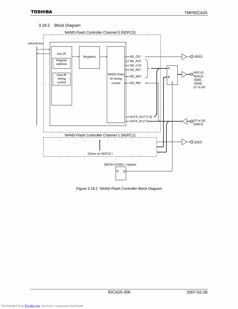
TMP92CA25
2007-02-28 92CA25-306
3.18.2 Block Diagram
Figure 3.18.1 NAND-Flash Controller Block Diagram
Internal bus
bus I/F
Register address
Host I/F timing control
Registers
NAND-Flash I/F timing
control
ND_CE*ND_ALEND_CLEND_RE*
ND_WE*
ND_RB*
DATA_OUT [7:0]DATA_IN [7:0]
CE0ND
A B
S
NDCLE, NDALE, NDRE , NDWE , D7 to D0
D7 to D0, NDR/ B
CE1ND
NAND-Flash Controller Channel 0 (NDFC0)
NAND-Flash Controller Channel 1 (NDFC1)
(Same as NDFC0 )
D Q
NDCR<CHSEL> register
Downloaded from Elcodis.com electronic components distributor

TMP92CA25
2007-02-28 92CA25-307
3.18.3 Operation Description
3.18.3.1 Accessing NAND-Flash Memory
The NDFC accesses data on NAND Flash memory indirectly through its internal registers. It also contains the ECC calculating circuits. Please see 3.18.3.2 for details of the ECC. This section explains the operations for accessing the NAND Flash.
Basically, set the command in ND0FMCR and then read or write to ND0FDTR. The
read cycle for ND0FDTR is completed after the external read cycle for the NAND-Flash is finished. Likewise, the write cycle for ND0FDTR is completed after the external write cycle for the NAND-Flash is finished.
1) Initialize
The initialize sequence is as follows. (1) ND0FSPR: Set the low pulse width. (2) ND0FIMR: Set 0x81 if interrupt is required.
(Release interrupt mask)
2) Write The write sequence is as follows.
(1) ND0FMCR: Set 0x7C for ECC data reset. (2) Write 512 bytes
ND0FMCR: Set 0x9D for NDCLE signal enable and command mode. ND0FDTR: Set 0x80 for the serial data input command. ND0FMCR: Set 0x9E for NDALE signal enable and address mode. ND0FDTR: Write address. Set A [7:0], A [16:9], and A [24:17]. If it is
required, set A [25]. ND0FMCR: Set 0xBC for the data mode. ND0FDTR: Write 512 bytes data.
(3) Read ECC data ND0FMCR: Set 0xDC for the ECC data read mode. NDECCRD: Read 6 bytes ECC data. First data: LPR [7:0] Second data: LPR [15:8] Third data: CPR [5:0], 2’b11 Fourth data: LPR [23:16] Fifth data: LPR [31:24] Sixth data: CPR [11:6], 2’b11
Downloaded from Elcodis.com electronic components distributor

TMP92CA25
2007-02-28 92CA25-308
(4) Write 16-byte redundant data
ND0FMCR: Set 0x9C for the data mode without ECC calculation. ND0FDTR: Write 16-byte redundant data. D520: LPR [23:16] D521: LPR [31:24] D522: CPR [11:6], 2’b11 D525: LPR [7:0] D526: LPR [15:8] D527: CPR [5:0], 2’b11
(5) Run page program ND0FMCR: Set 0x9D for NDCLE signal enable and command mode. ND0FDTR: Set 0x10 for the page program command. ND0FMCR: Set 0x1C for NDALE signal disable. Wait several states (e.g., “NOP” × 10) ND0FSR: Check BUSY flag. If it is 0, go to the next. If it is 1, wait until it becomes 0.
(6) Read status ND0FMCR: Set 0x1D for NDCLE signal and command mode. ND0FDTR: Set 0x70 for Status read command. ND0FMCR: Set 0x1C for NDCLE signal disable. ND0FDTR: Read the Status data from the NAND-Flash.
(7) Repeat 1 to 6 for all other pages if required.
Downloaded from Elcodis.com electronic components distributor

TMP92CA25
2007-02-28 92CA25-309
3) Read
The read sequence is as follows. (1) ND0FMCR: Set 0x7C for ECC data reset. (2) Read 512 bytes
ND0FMCR: Set 0x1D for NDCLE signal enable and command mode. ND0FDTR: Set 0x00 for the read command. ND0FMCR: Set 0x1E for NDALE signal enable and address mode. ND0FDTR: Set A [7:0], A [16:9], and A [24:17]. If it is required, set A
[25]. ND0FMCR: Set 0x1C for NDALE signal disable. Wait several states (e.g., “NOP” × 10)
ND0FSR: Check BUSY flag. If it is 0, go to the next. If it is 1, wait until it becomes 0. ND0FMCR: Set 0x3C for the data mode with ECC calculation. ND0FDTR: Read 512-byte data. ND0FMCR: Set 0x1C for the data mode without ECC calculation. ND0FDTR: Read 16-byte redundant data.
(3) Read ECC data
ND0FMCR: Set 0x5C for the ECC data read mode. NDECCRD: Read 6-byte ECC data. First data: LPR [7:0] Second data: LPR [15:8] Third data: CPR [5:0], 2’b11 Fourth data: LPR [23:16] Fifth data: LPR [31:24] Sixth data: CPR [11:6], 2’b11
(4) Software routine: Compare ECC data and redundant data, run the error routine if error is generated.
(5) Read other pages ND0FMCR: Set 0x1C. ND0FSR: Check BUSY flag. If it is 0, go to the next. If it is 1, wait until it becomes 0.
Downloaded from Elcodis.com electronic components distributor
TMP92CA25
2007-02-28 92CA25-310
4) ID read
The ID read sequence is as follows.
(1) ND0FMCR: Set 0x1D for NDCLE signal enable and command mode. (2) ND0FDTR: Set 0x90 for the ID Read command. (3) ND0FMCR: Set 0x1E for NDALE signal enable and the address mode. (4) ND0FDTR: Set 0x00. (5) ND0FMCR: Set 0x1C for the data mode without ECC calculation. (6) ND0FDTR: Read Maker code. (7) ND0FDTR: Read Device code.
3.18.3.2 ECC Control
The NDFC contains the ECC calculating circuits. The circuits are controlled by ND0FMCR. This circuit executes ECC data calculation. However, ECC comparison and error correction is not executed. This must be executed using software.
The calculated ECC data can be read from the NDECCRD register when ND0FMCR
is 0xD0 (write mode) or 0x50 (read mode). This is 6-byte data, and six NDECCRD read operations are required. The order of the data is as follows.
First data: LPR [7:0] Second data: LPR [15:8] Third data: CPR [5:0], 2’b11 Fourth data: LPR [23:16] Fifth data: LPR [31:24] Sixth data: CPR [11:6], 2’b11
Downloaded from Elcodis.com electronic components distributor

TMP92CA25
2007-02-28 92CA25-311
3.18.4 Registers
Table 3.18.1 NAND-Flash Control Registers for Channel 0
Address Register Register Name 1D00H (1D00H to 1EFFH) ND0FDTR NAND-Flash data transfer register 1CB0H (1CB0H to 1CB5H) ND0ECCRD NAND-Flash ECC-code read register 1CC4H ND0FMCR NAND-Flash mode control register 1CC8H ND0FSR NAND-Flash status register 1CCCH ND0FISR NAND-Flash interrupt status register 1CD0H ND0FIMR NAND-Flash interrupt mask register 1CD4H ND0FSPR NAND-Flash strobe pulse width register 1CD8H ND0FRSTR NAND-Flash reset register
Table 3.18.2 NAND-Flash Control Registers for Channel 1
Address Register Register Name 1D00H (1D00H to 1EFFH) ND1FDTR NAND-Flash data transfer register 1CB0H (1CB0H to 1CB5H) ND1ECCRD NAND-Flash ECC-code read register 1CE4H ND1FMCR NAND-Flash mode control register 1CE8H ND1FSR NAND-Flash status register 1CECH ND1FISR NAND-Flash interrupt status register 1CF0H ND1FIMR NAND-Flash interrupt mask register 1CF4H ND1FSPR NAND-Flash strobe pulse width register 1CF8H ND1FRSTR NAND-Flash reset register
Table 3.18.3 NAND-Flash Control Registers
Address Register Register Name 01C0H NDCR NAND-Flash control register
Downloaded from Elcodis.com electronic components distributor
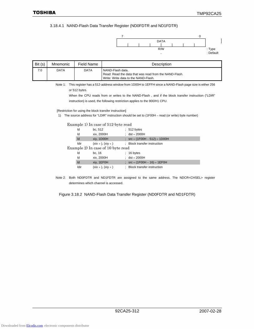
TMP92CA25
2007-02-28 92CA25-312
3.18.4.1 NAND-Flash Data Transfer Register (ND0FDTR and ND1FDTR)
7 0 DATA
R/W
− : Type : Default
Bit (s) Mnemonic Field Name Description
7:0 DATA DATA NAND-Flash data. Read: Read the data that was read from the NAND-Flash. Write: Write data to the NAND-Flash.
Note 1: This register has a 512-address window from 1D00H to 1EFFH since a NAND-Flash page size is either 256
or 512 bytes.
When the CPU reads from or writes to the NAND-Flash , and if the block transfer instruction (“LDIR”
instruction) is used, the following restriction applies to the 900/H1 CPU.
[Restriction for using the block transfer instruction] 1) The source address for “LDIR” instruction should be set to (1F00H – read (or write) byte number)
Example 1) In case of 512-byte read ld bc, 512 ; 512 bytes ld xix, 2000H ; dst = 2000H ld xiy, 1D00H ; src = (1F00H − 512) = 1D00H ldir (xix + ), (xiy + ) ; Block transfer instruction Example 2) In case of 16-byte read ld bc, 16 ; 16 bytes ld xix, 2000H ; dst = 2000H ld xiy, 1EF0H ; src = (1F00H − 16) = 1EF0H ldir (xix + ), (xiy + ) ; Block transfer instruction
Note 2: Both ND0FDTR and ND1FDTR are assigned to the same address. The NDCR<CHSEL> register
determines which channel is accessed.
Figure 3.18.2 NAND-Flash Data Transfer Register (ND0FDTR and ND1FDTR)
Downloaded from Elcodis.com electronic components distributor

TMP92CA25
2007-02-28 92CA25-313
3.18.4.2 NAND-Flash ECC-code Read Register (ND0ECCRD and ND1ECCRD)
7 0 ECC-code
R : Type − : Default
Bit (s) Mnemonic Field Name Description
7:0 ECC-code ECC-code Read calculated ECC data.
Note 1: Both ND0ECCRD and ND1ECCRD are assigned to the same address. The NDCR<CHSEL> register
determines which channel is accessed.
Figure 3.18.3 NAND-Flash ECC-code Read Register (ND0ECCRD and ND1ECCRD)
Downloaded from Elcodis.com electronic components distributor

TMP92CA25
2007-02-28 92CA25-314
3.18.4.3 NAND-Flash Mode Control Register (ND0FMCR and ND1FMCR)
7 6 5 4 3 5 1 0 WE ECC1 ECC0 CE PCNT1 PCNT0 ALE CLE
R/W R/W R/W R/W R/W R/W R/W R/W : Type
0 0 0 0 0 0 0 0 : Default
Bits Mnemonic Field Name Description 7 WE Write enable Write enable (Default: 0)
This bit enables the data write operation. When writing the data to the NAND-Flash, set this bit to “1”. When writing command or address, this bit need not be set to “1”. 0: Disable write operation 1: Enable write operation
6 ECC1
5 ECC0
ECC control ECC control (Default: 00) Control the ECC calculating circuits with <CE> (bit4) register. 11 (at<CE> = X): Reset ECC circuits 00 (at<CE> = 1): ECC circuits are disabled. 01 (at<CE> = 1): ECC circuits are enabled. 10 (at<CE> = 1): Read ECC data calculated by NDFC 10 (at<CE> = 0): Read ID data
4 CE Chip enable Chip enable (Default: 0) Enable NAND-Flash access. Set “1” to this bit when accessing the NAND-Flash. 0: Disable ( NDCE is High.) 1: Enable ( NDCE is Low.)
3 PCNT1 2 PCNT0
Power control Power control (Default: 00) Always write “11”
1 ALE Address latch enable
Address latch enable (Default: 0) This bit specifies the value of the NDALE signal. 0: Low 1: High
0 CLE Command latch enable
Command latch enable (Default: 0) This bit specifies the value of the NDCLE signal. 0: Low 1: High
Figure 3.18.4 NAND-Flash Mode Control Register (ND0FMCR and ND1FMCR)
Downloaded from Elcodis.com electronic components distributor

TMP92CA25
2007-02-28 92CA25-315
3.18.4.4 NAND-Flash Status Register (ND0FSR and ND1FSR)
7 6 0 BUSY
R : Type − : Default
Bits Mnemonic Field Name Description
7 BUSY BUSY BUSY (Default: Undefined) This bit shows the status of the NAND-Flash. 0: Ready 1: Busy
6:0 − − Reserved
Note: A noise-filter for some states is built into the NDFC, so when the NDR/ B pin changes, a <BUSY> flag is not
renewed at the same time. Therefore, insert several delays (e.g., “NOP” instruction × 10) using software before
starting this flag check.
Figure 3.18.5 NAND-Flash Status Register (ND0FSR and ND1FSR)
NDWE pin
Read command Address input Delay time Sensing <BUSY> flag
NDCLE pin
NDALE pin
NDR/ B pin
<BUSY> flag
Downloaded from Elcodis.com electronic components distributor

TMP92CA25
2007-02-28 92CA25-316
3.18.4.5 NAND-Flash Interrupt Status Register (ND0FISR and ND1FISR)
7 6 5 4 3 2 1 0 RDY
: Type : Default
Bits Mnemonic Field Name Description 7:1 − − Reserved 0 RDY Ready Ready (Default: 0)
When NDR/ B signal changes from low (BUSY) to High (READY) and NDFIMR<MRDY> is “1”, this bit is set to “1”. By writing “1”, this bit is cleared to 0. Read: 0: None 1: Change NDR/ B signal from BUSY to READY. Write: 0: No change 1: Clear to “0”
Figure 3.18.6 NAND-Flash Interrupt Status Register (ND0FISR and ND1FISR)
3.18.4.6 NAND-Flash Interrupt Mask Register (ND0FIMR and ND1FIMR)
7 6 4 3 2 1 0 INTEN 0 MRDY R/W R/W : Type
0 0 : Default
Bits Mnemonic Field Name Description 7 INTEN Interrupt enable Interrupt enable (Default: 0)
When <INTEN> and <MRDY> are set “1” and NDFISR<RDY> becomes “1”, INTNDFC occurs. 0: Disable 1: Enable
6:1 − − Reserved 0 MRDY Mask RDY
interrupt Mask RDY interrupt (Default: 0) This bit masks the NDFISR<RDY>. If <MRDY> is “1” and NDR/ B signal changes from Low to High, NDFISR<RDY> is set to “1”. 0: Disable to set NDFISR<RDY> 1: Enable to set NDFISR<RDY>
Figure 3.18.7 NAND-Flash Interrupt Mask Register (ND0FIMR and ND1FIMR)
Downloaded from Elcodis.com electronic components distributor

TMP92CA25
2007-02-28 92CA25-317
3.18.4.7 NAND-Flash Strobe Pulse Width Register (ND0FSPR and ND1FSPR)
7 6 5 4 3 2 1 0 SPW
R/W : Type 0000 : Default
Bits Mnemonic Field Name Description 7:4 − − Reserved 3:0 SPW Strobe pulse
width Strobe pulse width (Default: 0000) These bits set the Low pulse width of the NDRE and NDWE signals. The Low pulse width is ((value set to SPW) +1 )× fSYS clock
Figure 3.18.8 NAND-Flash Strobe Pulse Width Register (ND0FSPR and ND1FSPR)
Downloaded from Elcodis.com electronic components distributor

TMP92CA25
2007-02-28 92CA25-318
3.18.4.8 NAND-Flash Reset Register (ND0FRSTR and ND1FRSTR)
7 6 5 4 3 2 1 0 RST
R/W : Type 0 : Default
Bits Mnemonic Field Name Description 7:1 − − Reserved 0 RST Reset Reset (Default: 0)
By setting this bit, reset the NDFC (except NDCR<CHSEL> register). By reset, this bit is automatically cleared to “0”. 0: Don’t care 1: Reset
Note: After writing <RST> register, several waits are required (about 10 states) before accessing the NDFC.
Figure 3.18.9 NAND-Flash Reset Register (ND0FRSTR and ND1FRSTR)
3.18.4.9 NAND-Flash Control Register (NDCR)
7 6 5 4 3 2 1 0 Bit symbol CHSEL NDCR
(01C0H) Read/Write R/W After reset 0 Function 0: Channel 0
1: Channel 1
Downloaded from Elcodis.com electronic components distributor

TMP92CA25
2007-02-28 92CA25-319
3.18.5 Timing Diagrams
3.18.5.1 Command and Address Cycle
Figure 3.18.10 Command and Address Cycle
ND
CLE
ND
CE
D7
to D
0
ND
R/B
ND
ALE
ND
RE
ND
WE
ND0FMCR<CLE> = 0 ND0FMCR<ALE> = 1
ND0FMCR<CLE> = 1
ND0FMCR<CE> = 1
ND0FMCR<ALE> = 0
Downloaded from Elcodis.com electronic components distributor
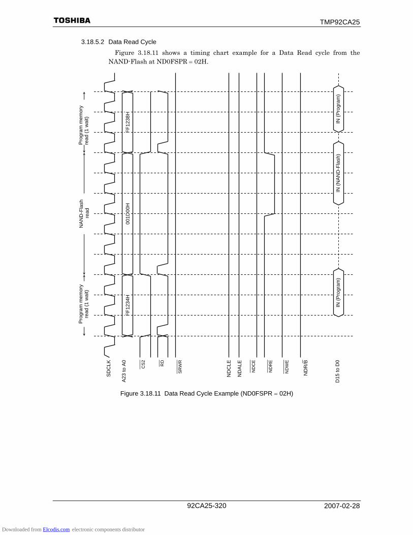
TMP92CA25
2007-02-28 92CA25-320
3.18.5.2 Data Read Cycle
Figure 3.18.11 shows a timing chart example for a Data Read cycle from the NAND-Flash at ND0FSPR = 02H.
Figure 3.18.11 Data Read Cycle Example (ND0FSPR = 02H)
IN (P
rogr
am)
IN (N
AN
D-F
lash
) IN
(Pro
gram
)
ND
CE
D15
to D
0
ND
R/B
ND
ALE
ND
RE
ND
WE
FF12
34H
00
1D00
H
FF12
38H
SD
CLK
A23
to A
0
CS
2
RD
SR
WR
Pro
gram
mem
ory
read
(1 w
ait)
NA
ND
-Fla
sh
read
P
rogr
am m
emor
y re
ad (1
wai
t)
ND
CLE
Downloaded from Elcodis.com electronic components distributor

TMP92CA25
2007-02-28 92CA25-321
3.18.5.3 Data Write Cycle
Figure 3.18.12 shows a timing chart example for a Data Write cycle to the NAND-Flash at ND0FSPR = 02H.
Figure 3.18.12 Data Write Cycle (ND0FSPR = 02H)
IN (P
rogr
am)
OU
T (N
AN
D-F
lash
) IN
(Pro
gram
)
ND
CE
D15
to D
0
ND
R/B
ND
ALE
ND
RE
ND
WE
FF12
34H
00
1D00
H
FF12
38H
SD
CLK
A23
to A
0
CS
2
RD
SR
WR
Pro
gram
mem
ory
read
(1 w
ait)
NA
ND
-Fla
sh
writ
e P
rogr
am m
emor
y re
ad (1
wai
t)
ND
CLE
Downloaded from Elcodis.com electronic components distributor

TMP92CA25
2007-02-28 92CA25-322
3.18.6 Example of NAND-Flash Use
Note 1: By reset, both NDRE and NDWE pins become input ports (Port 71 and Port 72) And so require pull-up
resistors.
Note 2: Use the NAND-Flash memory and board capacitance to set the correct value for the NDR/ B pin
pull-up resistor . 2 kΩ is a typical value.
Note 3: The NAND-Flash WP (write protect) pin is not supported by the TMP92CA25.
It must be provided by an external circuit if required.
Figure 3.18.13 Example of NAND-Flash Connection
TMP92CA25
NDCLE NDALE
NDRE
NDWE
NDR/ B D [7:0]
CE0ND CE1ND
External circuits for write protect
NAND-Flash 0 NAND-Flash 1
CLE ALE RE WE R/B (Open drain) I/O [7:0]
CE WP
CLE ALE RE WE R/B (Open drain) I/O [7:0]
CE WP
2 kΩ
100 kΩ
Downloaded from Elcodis.com electronic components distributor
TMP92CA25
2007-02-28 92CA25-323
3.19 16-Bit Timer/Event Counters (TMRB0)
The TMP92CA25 incorporates one multifunctional 16-bit timer/event counter (TMRB0) which has the following operation modes:
• 16-bit interval timer mode • 16-bit event counter mode • 16-bit programmable pulse generation (PPG) mode
The timer/event counter consists of a 16-bit up counter, two 16-bit timer registers (one of
them with a double buffer structure), a 16-bit capture register, two comparators, a capture input controller, a timer flip-flop and a control circuit.
The timer/event counter is controlled by an 11-byte control SFR. This chapter includes the following sections:
3.19.1 Block Diagrams 3.19.2 Operation of Each Block 3.19.3 SFRs 3.19.4 Operation in Each Mode
(1) 16-bit interval timer mode (2) 16-bit programmable pulse generation (PPG) output mode
Table 3.19.1 Pins and SFR of TMRB0
ChannelSpec.
TMRB0
External clock/capture trigger input pins None
External pins
Timer flip-flop output pins TB0OUT0 (also used as PC2)
Timer run register TB0RUN (1180H) Timer mode register TB0MOD (1182H) Timer flip-flop control register TB0FFCR (1183H)
TB0RG0L (1188H) TB0RG0H (1189H) TB0RG1L (118AH)
Timer register
TB0RG1H (118BH) TB0CP0L (118CH) TB0CP0H (118DH) TB0CP1L (118EH)
SFR (Address)
Capture register
TB0CP1H (118FH)
Downloaded from Elcodis.com electronic components distributor

TMP92CA25
2007-02-28 92CA25-324
3.19.1 Block Diagrams
Figure 3.19.1 Block Diagram of TMRB0
Inte
rnal
dat
a bu
s
Sle
lect
or
16-b
it co
mpa
rato
r (C
P10
)
TB0M
OD
<TB
0CLK
1:0>
φT1
φT4
φT16
Tim
er
flip-
flop
cont
rol
TB0F
F0
TB0O
UT0
Mat
ch
dete
ctio
n
16-b
it tim
er re
gist
er
TB0R
G0H
/L
R
egis
ter b
uffe
r 10
TA1O
UT
TB1M
OD
<T
B0C
PM
1:0>
16-b
it tim
e re
gist
er
TB0R
G1H
/L
TB0M
OD
<TB
0CP
0I>
16-b
it co
mpa
rato
r (C
P11
)
Cap
ture
, ex
tern
al in
terr
upt
inpu
t con
trol
TB0R
UN
<TB
0RU
N>
Cap
utur
e re
gist
er 1
TB
0CP
1H/L
C
aptu
re re
gist
er 0
TB
0CP
0H/L
Run
/ cl
ear
Inte
rnal
dat
a bu
s
Mat
ch d
etec
tion
16-b
it up
cou
nter
(U
C10
)
Cou
nt
cloc
k
(from
TM
RA0
1)
Pre
scal
er
cloc
k: φ
T0
32
16
8 4
2 φT1
φT4
φT16
TB0R
UN
<T
B0P
RU
N>
Inte
rnal
dat
a bu
s
TB0M
OD
<TB
0CLE
> Inte
nal d
ata
bus
Ove
rflow
in
terr
upt
INTT
BO
F0
Tim
er
flip-
flop
Tim
er fl
ip-fl
op
outp
ut
Inte
rrup
t out
put
INTT
B00
IN
TTB
01
TB0R
UN
<T
B0R
DE
>
Downloaded from Elcodis.com electronic components distributor
TMP92CA25
2007-02-28 92CA25-325
3.19.2 Operation of Each Block
(1) Prescaler The 5-bit prescaler generates the source clock for timer 0. The prescaler clock (φT0) is
a divided clock (divided by 8) from the fFPH. This prescaler can be started or stopped using TB0RUN<TB0PRUN>. Counting
starts when <TB0PRUN> is set to “1”; the prescaler is cleared to 0 and stops operation when <TB0PRUN> is cleared to “0”.
Table 3.19.2 Prescaler Clock Resolution
Timer counter input clock TMRB prescaler
TB0MOD<TB0CLK1:0>
System clock selection
SYSCR1
<SYSCK>
Clock gear selection
SYSCR1
<GEAR2:0>
−
φT1(1/2) φT4 (1/8) φT16 (1/32) 1 (fs) − fs/16 fs/64 fs/256
000 (1/1) fc/16 fc/64 fc/256 001 (1/2) fc/32 fc/128 fc/512 010 (1/4) fc/64 fc/256 fc/1024 011 (1/8) fc/128 fc/512 fc/2048
0 (fc)
100 (1/16)
1/8
fc/256 fc/1024 fc/4096
XXX: Don't care
(2) Up counter (UC10) UC10 is a 16-bit binary counter which counts up pulses input from the clock specified
by TB0MOD<TB0CLK1:0>. Any one of the prescaler internal clocks φT1, φT4 and φT16 can be selected as the
input clock. Counting or stopping and clearing of the counter is controlled by TB0RUN<TB0RUN>.
When clearing is enabled, the up counter UC10 will be cleared to “0” each time its value matches the value in the timer register TB0RG1H/L. If clearing is disabled, the counter operates as a free-running counter.
Clearing can be enabled or disabled using TB0MOD<TB0CLE>. A timer overflow interrupt (INTTBOF0) is generated when UC10 overflow occurs.
Downloaded from Elcodis.com electronic components distributor

TMP92CA25
2007-02-28 92CA25-326
(3) Timer registers (TB0RG0H/L and TB0RG1H/L)
These 16-bit registers are used to set the interval time. When the value in the up counter UC10 matches the value set in this timer register, the comparator match detect signal will go active.
Setting data for both Upper and Lower timer registers is always needed. For example, either using a 2-byte data transfer instruction or using a 1-byte data transfer instruction twice for the lower 8 bits and upper 8 bits in order.
The TB0RG0H/L timer register has a double-buffer structure, which is paired with a register buffer. The value set in TB0RUN<TB0RDE> determines whether the double-buffer structure is enabled or disabled: it is disabled when <TB0RDE> = “0”, and enabled when <TB0RDE> = “1”.
When the double buffer is enabled, data is transferred from the register buffer to the timer register when the values in the up counter (UC10) and the timer register TB0RG1H/L match.
After a reset, TB0RG0H/L and TB0RG1H/L are undefined. If the 16-bit timer is to be used after a reset, data should be written to it beforehand.
On a reset <TB0RDE> is initialized to “0”, disabling the double buffer. To use the double buffer, write data to the timer register, set <TB0RDE> to 1, then write data to the register buffer as shown below.
TB0RG0H/L and the register buffer both have the same memory addresses (001188H and 001189H) allocated to them. If <TB0RDE> = “0”, the value is written to both the timer register and the register buffer. If <TB0RDE> = “1”, the value is written to the register buffer only.
The addresses of the timer registers are as follows:
The timer registers are write-only registers and thus cannot be read.
TMRB0
TB0RG0H/L Upper 8 bits (TB0RG0H)
Lower 8 bits(TB0RG0L)
001189H 001188H
TB0RG1H/LUpper 8 bits(TB0RG1H)
Lower 8 bits(TB0RG1L)
00118BH 00118AH
Downloaded from Elcodis.com electronic components distributor

TMP92CA25
2007-02-28 92CA25-327
(4) Capture registers (TB0CP0H/L and TB0CP1H/L)
These 16-bit registers are used to latch the values in the up counters. All 16 bits of data in the capture registers should be read. For example, using a
2-byte data load instruction or two 1-byte data load instructions. The least significant byte is read first, followed by the most significant byte.
The addresses of the capture registers are as follows:
The capture registers are read-only registers and thus cannot be written to.
(5) Capture input control This circuit controls the timing to latch the value of the up counter UC10 into
TB0CP0H/L and TB0CP1H/L. The value in the up counter can be loaded into a capture register by software.
Whenever “0” is programmed to TB0MOD<TB0CP0I>, the current value in the up counter is loaded into capture register TB0CP0H/L. It is necessary to keep the prescaler in run mode (i.e., TB0RUN<TB0PRUN> must be held at a value of 1).
(6) Comparators (CP10 and CP11) CP10 and CP11 are 16-bit comparators which compare the value in the up counter
UC10 with the value set in TB0RG0H/L or TB0RG1H/L respectively, in order to detect a match. If a match is detected, the comparator generates an interrupt (INTTB00 or INTTB01 respectively).
(7) Timer flip-flops (TB0FF0) These flip-flops are inverted by the match detect signals from the comparators and
the latch signals to the capture registers. Inversion can be enabled and disabled for each element using TB0FFCR<TB0C0T1, TB0E1T1 and TB0E0T1>.
After a reset the value of TB0FF0 is undefined. If “00” is programmed to TB0FFCR <TB0FF0C1:0>, TB0FF0 will be inverted. If “01” is programmed to the capture registers, the value of TB0FF0 will be set to “1”. If “10” is programmed to the capture registers, the value of TB0FF0 will be cleared to “0”.
The values of TB0FF0 can be output via the timer output pin TB0OUT0 (which is shared with PC6). Timer output should be specified using the port B function register.
TMRB0
TB0CP0H/L Upper 8 bits (TB0CPH)
Lower 8 bits(TB0CP0L)
00118DH 00118CH
TB0CP1H/LUpper 8 bits(TB0CP1H)
Lower 8 bits(TB0CP1L)
00118FH 00118EH
Downloaded from Elcodis.com electronic components distributor
TMP92CA25
2007-02-28 92CA25-328
3.19.3 SFRs
TMRB0 Run Register
7 6 5 4 3 2 1 0 Bit symbol TB0RDE − I2TB0 TB0PRUN TB0RUNTB0RUN
(1180H) Read/Write R/W R/W R/W After reset 0 0 0 0 0
TMRB0 Prescaler
Up counter UC10
Function Double buffer 0: Disable 1: Enable
Always write “0”
IDLE2 0: Stop 1: Operate 0: Stop and clear
1: Run (Count up)
Count operation 0 Stop and clear 1 Count
Note: 1, 4 and 5 of TB0RUN are read as undefined values.
Figure 3.19.2 The Registers for TMRB
Downloaded from Elcodis.com electronic components distributor

TMP92CA25
2007-02-28 92CA25-329
TMRB0 Mode Register
7 6 5 4 3 2 1 0 Bit symbol − − TB0CP0I TB0CPM1 TB0CPM0 TB0CLE TB0CLK1 TB0CLK0TB0MOD
(1182H) Read/Write R/W W* R/W After reset 0 0 1 0 0 0 0 0 Function Always write “0” Execute
software capture 0: Software capture 1: Undefined
Capture timing 00: Disable 01: Reserved 10: Reserved 11: TA1OUT↑ TA1OUT↓
Control up counter 0: Disable clearing 1: Enable clearing
TMRB0 source clock 00: Reserved 01: φT1 10: φT4 11: φT16
TMRB0 source clock 00 Reserved 01 φT1 10 φT4 11 φT16
Up counter clear control 0 Disable 1 Enable clearing on match with TB0RG1H/L
Capture/interrupt timing 00 Disable 01 Reserved 10 Reserved 11 Capture to TB0CP0H/L at rising edge of TA1OUT
Capture to TB0CP1H/L at falling edge of TA1OUT
Software capture 0 The value in the up counter is captured to
TB0CP0H/L. 1 Undefined
Figure 3.19.3 The Registers for TMRB0
Read-modify-write instruction is prohibited.
Downloaded from Elcodis.com electronic components distributor

TMP92CA25
2007-02-28 92CA25-330
TMRB0 Flip-Flop Control Register
7 6 5 4 3 2 1 0 Bit symbol − − TB0C1T1 TB0C0T1 TB0E1T1 TB0E0T1 TB0FF0C1 TB0FF0C0TB0FFCR
(1183H) Read/Write W* R/W W* After reset 1 1 0 0 0 0 1 1
TB0FF0 inversion trigger 0: Disable trigger 1: Enable trigger
Function Always write “11”.
Invert when the UC value is loaded into TB0CP1H/L.
Invert when the UC value is loaded into TB0CP0H/L.
Invert when the UC value matches the value in TB0RG1H/L.
Invert when the UC value matches the value in TB0RG0H/L.
Control TB0FF0 00: Invert 01: Set 10: Clear 11: Don’t care * Always read as 11.
Timer flip-flop control (TB0FF0) 00 Invert 01 Set to 1
10 Clear to 0 11 Don’t care
Inverted when the UC10 value matches the value in TB0RG0H/L.
0 Disable trigger 1 Enable trigger
Inverted when the UC10 value matches the value in TB0RG1H/L.
0 Disable trigger 1 Enable trigger
Inverted when the UC10 value is loaded into TB0CP0. 0 Disable trigger 1 Enable trigger
Inverted when the UC10 value is loaded into TB0CP1H/L. 0 Disable trigger 1 Enable trigger
Figure 3.19.4 The Registers for TMRB
Read-modify-write instruction is prohibited.
Downloaded from Elcodis.com electronic components distributor

TMP92CA25
2007-02-28 92CA25-331
TMRB0 register
7 6 5 4 3 2 1 0 bit Symbol - Read/Write W
TB0RG0L (1188H) After reset Undefined
bit Symbol - Read/Write W
TB0RG0H (1189H) After reset Undefined
bit Symbol - Read/Write W
TB0RG1L (118AH) After reset Undefined
bit Symbol - Read/Write W
TB0RG1H (118BH) After reset Undefined
bit Symbol - Read/Write W
TB0CP0L (118CH)
After reset Undefined
bit Symbol - Read/Write W
TB0CP0H (118DH)
After reset Undefined
bit Symbol - Read/Write W
TB0CP1L (118EH)
After reset Undefined
bit Symbol - Read/Write W
TB0CP1H (118FH)
After reset Undefined
Note: All registers are prohibited to execute read-modify-write instruction.
Figure 3.19.5 The Registers for TMRB
Downloaded from Elcodis.com electronic components distributor

TMP92CA25
2007-02-28 92CA25-332
3.19.4 Operation in Each Mode
(1) 16-bit interval timer mode Generating interrupts at fixed intervals.
In this example, the interrupt INTTB01 is set to be generated at fixed intervals. The interval time is set in the timer register TB0RG1H/L.
7 6 5 4 3 2 1 0 TB0RUN ← 0 0 X X − 0 X 0 Stop TMRB0. INTETB01 ← X 1 0 0 X 0 0 0 Enable INTTB01 and set interrupt level 4. Disable INTTB00. TB0FFCR ← 1 1 0 0 0 0 1 1 Disable the trigger. TB0MOD ← 0 0 1 0 0 1 * * Select internal clock for input and disable the capture function. (** = 01, 10, 11) TB0RG1 ← * * * * * * * * * * * * * * * *
Set the interval time (16 bits).
TB0RUN ← 0 0 X X − 1 X 1 Start TMRB0. X: Don't care, −: No change
(2) 16-bit programmable pulse generation (PPG) output mode
Square wave pulses can be generated at any frequency and duty ratio. The output pulse may be either low active or high active.
The PPG mode is obtained by inversion of the timer flip-flop TB0FF0 that is enabled by the match of the up counter UC10 with timer register TB0RG0H/L or TB0RG1H/L and is output to TB0OUT0. In this mode the following conditions must be satisfied.
(Value set in TB0RG0H/L) < (Value set in TB0RG1H/L)
Figure 3.19.6 Programmable Pulse Generation (PPG) Output Waveforms
When the TB0RG0H/L double buffer is enabled in this mode, the value of register buffer 10 will be shifted into TB0RG0H/L at match with TB0RG1H/L. This feature facilitates the handling of low duty waves.
Figure 3.19.7 Operation of Register Buffer
Match with TB0RG0H/L(INTTB00 inerrupt)
Match with TB0RG1H/L(INTTB01 interrupt)
TB0OUT0 pin
Q2 Q1
Match with TB0RG0H/L
Q3 Q2
Up counter = Q1 Up counter = Q2
Shift into TB0RG1H/L TB0RG0H/L
(Value to be compared)
Register buffer
Match with TB0RG1H/L
Write TB0RG0H/L
Downloaded from Elcodis.com electronic components distributor
TMP92CA25
2007-02-28 92CA25-333
The following block diagram illustrates this mode.
Figure 3.19.8 Block Diagram of 16-Bit Mode
The following example shows how to set 16-bit PPG output mode:
7 6 5 4 3 2 1 0 TB0RUN ← 0 0 X X − 0 X 0 Disable the TB0RG0H/L double buffer and stop TMRB0.
* * * * * * * * TB0RG0H/L ←* * * * * * * *
Set the duty ratio (16 bits).
* * * * * * * * TB0RG1H/L ←* * * * * * * *
Set the frequency (16 bits).
TB0RUN ← 1 0 X X − 0 X 0 Enable the TB0RG0H/L double buffer. (The duty and frequency are changed on an INTTB01 interrupt.)
TB0FFCR ← 1 1 0 0 1 1 1 0 Set the mode to invert TB0FF0 at the match with TB0RG0H/L/TB0RG1H/L. Set TB0FF0 to “0”.
TB0MOD ← 0 0 1 0 0 1 * * Select the Prescaler output clock as the input clock and disable (** = 01, 10, 11) the capture function. PCCR ← − 1 X X − − − − PCFC ← − 1 X X − − − −
Set PC6 to function as TB0OUT0.
TB0RUN ← 1 0 X X − 1 X 1 Start TMRB0. X: Don't care, −: No change
Selector
16-bit up counter UC10
16-bit comparator 16-bit comparator
φT1φT4
φT16
F/F (TB0FF0)
TB0RG0H/L
Register buffer 10 TB0RG1H/L TB0RUN<TB0RDE>
TB0RG0-WR
TB0RUN<TB0RUN> TB0OUT0 (PPG output)
Internal data bus
Clear
Match
Selector
Downloaded from Elcodis.com electronic components distributor

TMP92CA25
2007-02-28 92CA25-334
3.20 Touch Screen Interface (TSI)
The TMP92CA25 has an interface for a 4-terminal resistor network touch screen. This interface supports two procedures: an X/Y position measurement and touch detection. Each procedure is executed by setting the TSI control register (TSICR0 and TSICR1) and
using an internal AD converter.
3.20.1 Touch Screen Interface Module Internal/External Connection
Figure 3.20.1 External Connection of TSI
Figure 3.20.2 Internal Block Diagram of TSI
Touch screen
Y+
Y−
X−
X+
MY
MX
PY
PX
TMP92CA25
External capacitors
PXEN
PYEN
MXEN INT4
MYEN PTST
TSI7
Touch screen control
AN3
AN2
AVCC
AVSS
VREFH
VREFL
AD converter
Dec.SPXSPY
SMYSMX
PXD (typ.200 kΩ)
Inte
rnal
dat
a bu
s
AVCC
AVSS
P97 (PY)
P96/INT4 (PX)
PG3/AN3 (MY)
PG2/AN2 (MX)
VREFH
VREFL
Downloaded from Elcodis.com electronic components distributor

TMP92CA25
2007-02-28 92CA25-335
3.20.2 Touch Screen Interface (TSI) Control Register
TSI Control Register
7 6 5 4 3 2 1 0 Bit symbol TSI7 PTST TWIEN PYEN PXEN MYEN MXEN TSICR0
(01F0H) Read/Write R/W R R/W After reset 0 0 0 0 0 0 0 Function 0: Disable
1: Enable Detection
condition 0: no touch1: touch
INT4 interrupt control 0: Disable 1: Enable
SPY 0 : OFF 1 : ON
SPX 0 : OFF 1 : ON
SMY 0 : OFF 1 : ON
SMX 0 : OFF 1 : ON
PXD (Internal Pull-down resistance) ON/OFF setting
<PXEN>
<TSI7> 0 1
0 OFF OFF 1 ON OFF
Debounce Time Setting Register
7 6 5 4 3 2 1 0 Bit symbol DBC7 DB1024 DB256 DB64 DB8 DB4 DB2 DB1 TSICR1
(01F1H) Read/Write R/W After reset 0 0 0 0 0 0 0 0
1024 256 64 8 4 2 1 Function 0: Disable 1: Enable Debounce time is set by the formula “(N × 64 − 16)/fSYS”.
“N” is the number of bits between bit6 and bit0 which are set to “1”. Note2)
Note1: Since an internal clock is used for the debounce circuit, when IDLE1, STOP mode, the de-bounce circuit
don’t operate and also interrupt which through this circuit is not generated. When IDLE1, STOP mode, set
this circuit to disable (Write “0” to TSICR1<DBC7>) before entering HALT state.
Note2: Ex:
TSICR1=95H →N = 64 + 4 + 1 = 69
Downloaded from Elcodis.com electronic components distributor

TMP92CA25
2007-02-28 92CA25-336
3.20.3 Touch Detection Procedure
The Touch detection procedure shows procedure until a pen is touched by the screen and it is detected.
By touching, TSI generates interrupt (INT4) and this procedure terminates. After an X/Y position measuring procedure is terminated, return to this procedure and wait for the next touch.
When the waiting state, make ON only the SPY switch ON and OFF the other 3 switches (SMY, SPX and SMX).
The pull-down resistor that is connected to the P96/INT4/PX pin is ON when the SPX switch is OFF.
During this waiting state, P96/INT4/PX pin’s level is L because the internal Pull-down resistors (PXD) between the X and Y directions in the touch screen are not connected and INT4 is not generated.
When the pen touches the screen, P96/INT4/PX pin’s level is H because the internal resistors between the X and Y directions in the touch screen are connected and INT4 is generated.
In order to avoid the generation of several interrupts from one touch, a debounce circuit is used, as below.
This can ignore the pulse under the time which is set to TSICR1 register. The circuit detects the rising of signal, counts-up the time of the counter which is set,
after count, receive the signal internal. During counting, when the signal is set to Low, counter is cleared. And the state become to state of waiting a rising edge.
Figure 3.20.3 Block Diagram of Debounce Circuit
Debounce circuit
TSICR1
Enables INT4 and selects the Rising edge or
Falling edge of INT4 INT4
TSICR0<PTST>
F/F
TSICR0<TWIEN>, IIMC<I4EDGE>, P9FC<P96F>
P96/INT4/PX pin
Downloaded from Elcodis.com electronic components distributor

TMP92CA25
2007-02-28 92CA25-337
Figure 3.20.4 Timing Diagram of Debounce Circuit
Debouncetime
Debouncetime
Debounce time
INT4
INT4 is generated by matching counter and specified debounce time.
IINT4 is not generated by matching counter and specified debounce period because it is an edge-type interrupt.
After pen is released, INT4 can be issued again.
Reset counter for debounce time
Start counter for debounce time
Downloaded from Elcodis.com electronic components distributor
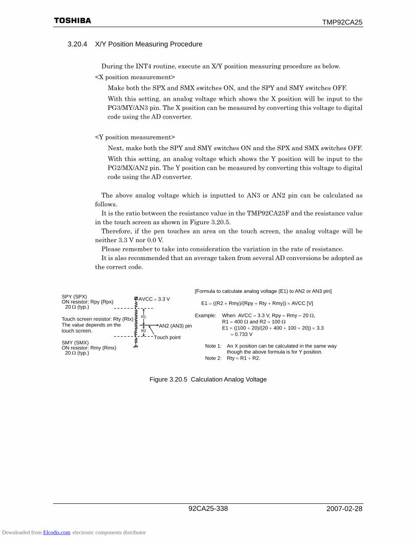
TMP92CA25
2007-02-28 92CA25-338
3.20.4 X/Y Position Measuring Procedure
During the INT4 routine, execute an X/Y position measuring procedure as below.
<X position measurement> Make both the SPX and SMX switches ON, and the SPY and SMY switches OFF. With this setting, an analog voltage which shows the X position will be input to the PG3/MY/AN3 pin. The X position can be measured by converting this voltage to digital code using the AD converter.
<Y position measurement>
Next, make both the SPY and SMY switches ON and the SPX and SMX switches OFF. With this setting, an analog voltage which shows the Y position will be input to the PG2/MX/AN2 pin. The Y position can be measured by converting this voltage to digital code using the AD converter.
The above analog voltage which is inputted to AN3 or AN2 pin can be calculated as
follows. It is the ratio between the resistance value in the TMP92CA25F and the resistance value
in the touch screen as shown in Figure 3.20.5. Therefore, if the pen touches an area on the touch screen, the analog voltage will be
neither 3.3 V nor 0.0 V. Please remember to take into consideration the variation in the rate of resistance. It is also recommended that an average taken from several AD conversions be adopted as
the correct code.
Figure 3.20.5 Calculation Analog Voltage
R2
R1
AN2 (AN3) pin
Touch point
Touch screen resistor: Rty (Rtx)The value depends on the touch screen.
SMY (SMX) ON resistor: Rmy (Rmx)
20 Ω (typ.)
SPY (SPX) ON resistor: Rpy (Rpx)
20 Ω (typ.) AVCC = 3.3 V
[Formula to calculate analog voltage (E1) to AN2 or AN3 pin]
E1 = ((R2 + Rmy)/(Rpy + Rty + Rmy)) × AVCC [V] Example: When AVCC = 3.3 V, Rpy = Rmy = 20 Ω,
R1 = 400 Ω and R2 = 100 Ω E1 = ((100 + 20)/(20 + 400 + 100 + 20)) × 3.3 = 0.733 V
Note 1: An X position can be calculated in the same way
though the above formula is for Y position. Note 2: Rty = R1 + R2.
Downloaded from Elcodis.com electronic components distributor

TMP92CA25
2007-02-28 92CA25-339
3.20.5 Flow Chart for TSI
Figure 3.20.6 Flow Chart for TSI Following pages explain each circuit condition of (a), (b) and (c) in above flow chart.
Main routine:
Execute main routine
TSICR0 ← 98H TSICR1 ← XXH (Voluntary)
INT4 routine:
<X position measurement>・TSICR0 ← 85H ・AD conversion for AN3 ・Store the result
<Y position measurement>・TSICR0 ← 8AH ・AD conversion for AN2 ・Store the result
Execute an operation by using X/Y position
Still touched ? TSICR0<PTST> = 1?
Return to main routine
No
Yes
(1) Touch detection procedure (2) X/Y position measurement procedure
Downloaded from Elcodis.com electronic components distributor
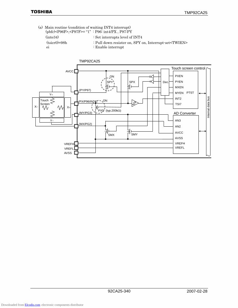
TMP92CA25
2007-02-28 92CA25-340
(a) Main routine (condition of waiting INT4 interrupt)
(pbfc)<P96F>,<P97F>= “1” : P96: int4/PX , P97:PY (inte34) : Set interrupts level of INT4
(tsicr0)=98h : Pull down resister on, SPY on, Interrupt-set<TWIEN> ei : Enable interrupt
AVSS
(PX/P96/INT4)
(PY/P97)
VREFH VREFL
PXEN
PYEN
MXEN
MYEN
AN3
AN2
(MY/PG3)
AVCC
(MX/PG2)
VREFH VREFL
AVCC
AVSS
AD Converter
Touch screen control
TSI7
SPY SPX
SMX SMY
PXD (typ.200kΩ)
Dec.
INT2
PTST
Inte
rnal
dat
a bu
s
Y+
Y−
Touch Screen
X+ X−
TMP92CA25
ON
ON
Downloaded from Elcodis.com electronic components distributor

TMP92CA25
2007-02-28 92CA25-341
(b) X position measurement (Start A/D conversion)
(tsicr0)=85h : SMX, SPX on (admod1)=83h : AN3 measure (admod0)=01h : A/D start
AVSS
(PX/P96/INT4)
(PY/P97)
VREFH VREFL
PXEN
PYEN
MXEN
MYEN
AN3
AN2
(MY/PG3)
AVCC
(MX/PG2)
VREFH VREFL
AVCC
AVSS
AD Converter
Touch screen control
TSI7
SPY SPX
SMX SMY
PXD (typ.200kΩ)
Dec
INT2
PTST
Inte
rnal
dat
a bu
s
Y+
Y−
Touch Screen
X+ X−
TMP92CA25
ON
ON
Downloaded from Elcodis.com electronic components distributor

TMP92CA25
2007-02-28 92CA25-342
(c) Y position measurement (Start A/D conversion)
(tsicr0)=8ah : SMY, SPY on (admod1)=82h : AN2 measure (admod0)=01h : A/D start
AVSS
(PX/P96/INT4)
(PY/P97)
VREFH VREFL
PXEN
PYEN
MXEN
MYEN
AN3
AN2
(MY/PG3)
AVCC
(MX/PG2)
VREFH VREFL
AVCC
AVSS
AD Converter
Touch screen control
TSI7
SPY SPX
SMX SMY
PXD (typ.200kΩ)
Dec.
INT2
PTST
Inte
rnal
dat
a bu
s
Y+
Y−
TouchScreen
X+ X−
TMP92CA25
ON
ON
Downloaded from Elcodis.com electronic components distributor

TMP92CA25
2007-02-28 92CA25-343
3.21 I2S (Inter-IC Sound)
An I2S format compatible serial output circuit is built-in. This product can be used in digital audio system applications by connecting LSI for sound
generation (e.g., a DA converter). This circuit has both I2S mode and general SIO mode. But both modes have only clock output
and data transmitting functions. Table 3.21.1 shows an outline for each mode.
Table 3.21.1 Outline for Each Mode
I2S mode SIO mode 1) Format I2S-format compatible
(Only master and transmitting)General
(Only master and transmitting) 2) Used pin 1. I2SCKO (Clock output)
2. I2SDO (Clock output) 3. I2SWS (Word select output)
1. I2SCKO (Clock output) 2. I2SDO (Data output)
3) WS frequency Selectable either fs/4 or TA1OUT (TMRA1 output) −
4) Baud rate (at fc = 40 MHz) Selectable either 20, 10, 5, or 2.5 Mbps
5) Transmittion buffer 16 bytes × 2 channels (Right, left) 32 bytes 6) Direction of data Selectable either MSB first or LSB first 7) Data length Selectable either 8 bits or 16 bits 8) Edge of clock Selectable either rising edge or falling edge 9) Interrupt INTI2S (FIFO empty interrupt)
Downloaded from Elcodis.com electronic components distributor

TMP92CA25
2007-02-28 92CA25-344
3.21.1 Block Diagram
Figure 3.21.1 I2S Block Diagram
2 4 8 Prescaler
fSYS
Sel
ecto
r
<MCK1:0>
I2SCKO control
<TXE, CLKE>
I2SCKO
Sel
ecto
r
<I2SWCK>
I2SWS control
<FMT, I2SWLVL>
I2SWS ÷ 4 fS
TA1OUT
Data selector,interrupt control
<BUSY>
FIFO control
FIFO control
I2S
BU
FR
I2S
BU
FL
Write pointer Read pointer
Write pointer Read pointer
I2S
CTL
0
16 bits
16 bits
16 bits
Inte
rnal
dat
a bu
s
<FMT><I2SFSEL><DIR> <BIT>
Shi
fter
<DIR>
I2SDO
INTI2S
0 1 7
16-byte FIFO (Left)(2 bytes × 8)
0 1 7
16-byte FIFO (Right)(2 bytes × 8)
Downloaded from Elcodis.com electronic components distributor

TMP92CA25
2007-02-28 92CA25-345
3.21.2 SFR
The following tables show the SFR for I2S. This I2S is connected to the CPU by the 16-bit data bus. When the CPU accesses the SFR, use a 2-byte load instruction.
I2SCTL0 Register
7 6 5 4 3 2 1 0 Bit symbol TXE FMT BUSY DIR BIT MCK1 MCK0 I2SWCKI2SCTL0
(080EH) Read/Write R/W R R/W After reset 0 0 0 0 0 0 0 0 Function Transmit
0: Stop 1: Start
Mode 0: I2S 1: SIO
Status 0: Stop
1: Under transmitting
First bit 0: MSB 1: LSB
Bit number0: 8 bits 1: 16 bits
Baud rate 00: fSYS 10: fSYS/4 01: fSYS/2 11: fSYS/8
WS clock
0: fs/4 1: TA1OUT
Note: <I2SWCK> is effective only for I2S mode.
15 14 13 12 11 10 9 8 Bit symbol I2SWLVL EDGE I2SFSEL I2SCLKE SYSCKE(080FH) Read/Write R/W R/W
After reset 0 0 0 0 0 Function WS level
0: Low left 1: High left
Clock edge for data out 0: Falling 1: Rising
Select for stereo 0: Stereo
(2 channels)
1: Monaural(1 channel)
Clock enable (After transmit) 0: Operation
1: Stop
System clock 0: Disable1: Enable
Note: <I2SWLVL>, <I2FSEL> and <I2SCLKE> are effective only in I2S mode.
I2SBUFR Register
15 14 13 12 11 10 9 8 7 6 5 4 3 2 1 0Bit symbol R15 R14 R13 R12 R11 R10 R9 R8 R7 R6 R5 R4 R3 R2 R1 R0I2SBUFR
(0800H) Read/Write W After reset Undefined Function Register for transmitting buffer (FIFO) (Right channel)
I2SBUFL Register
15 14 13 12 11 10 9 8 7 6 5 4 3 2 1 0Bit symbol L15 L14 L13 L12 L11 L10 L9 L8 L7 L6 L5 L4 L3 L2 L1 L0I2SBUFL
(0808H) Read/Write W After reset Undefined Function Register for transmitting buffer (FIFO) (Left channel)
Figure 3.21.2 I2S SFR
Read-modify-write instruction is prohibited
Read-modify-write instruction is prohibited
Downloaded from Elcodis.com electronic components distributor

TMP92CA25
2007-02-28 92CA25-346
3.21.3 Explanation of I2S Mode
(1) Connection example Figure 3.21.3 shows an example with external LSI.
Note: After reset, P90 to P92 are placed in a high-impedance state. Connect each pin with a pull-up or pull-down resistor as
necessary.
Figure 3.21.3 Example with External LSI
(2) Procedure A 32-byte FIFO is built-in. If the FIFO’s data becomes empty, an INTI2S interrupt is
generated. In the interrupt routine, write the next transmission data to the FIFO. The following shows a setting example and timing diagram.
(Setting example) Transmitting by I2S mode, I2SWS = 8.192 kHz, I2SCKO = 10 MHz, synchronous with rising edge (at fSYS = 20 MHz)
(Main routine) 7 6 5 4 3 2 1 0 INTE5I2S X 0 0 1 X − − − Set interrupts level. P9CR − − − − − 0 0 0 Set pins to P90 (I2SCKO), P91 (I2SDO), and P92 (I2SWS). P9FC − − − − − 1 1 1 I2SCTL0 0 0 − 0 0 0 1 0 Set I2S mode, MSB first, 8 bits, fSYS/2 clocks. 0 1 0 1 0 0 0 1 Set rising edge, clock stop. I2SBUFR ** ** ** ** ** ** ** ** Write 16-byte data to FIFO for right (8 times). I2SBUFL ** ** ** ** ** ** ** ** Write 16-byte data to FIFO for left (8 times). I2SCTL0 1 0 − 0 0 0 1 0 Start transmitting. 0 1 0 1 0 0 0 1
(INTI2S interrupt routine) I2SBUFR ** ** ** ** ** ** ** ** Write 16-byte data to FIFO for right (8 times). I2SBUFL ** ** ** ** ** ** ** ** Write 16-byte data to FIFO for left (8 times).
X: Don't care, −: No change
(Transmitter)
P92/I2SWS
P90/I2SCKO
P91/I2SDO
(Receiver) WS CK DATA
TMP92CA25
Example: DA converter
Downloaded from Elcodis.com electronic components distributor

TMP92CA25
2007-02-28 92CA25-347
Figure 3.21.4 Whole Timing Diagram
Figure 3.21.5 Detail Timing Diagram
(3) Notes 1) INTI2S timing
INTI2S is generated after the last data of FIFO is loaded to the internal shifter. FIFO is now empty and it is possible to write the next data.
2) I2SCTL0<TXE> A transmission is started by programming “1” to the <TXE> register and
stopped by writing “0”. After<TXE> is programmed “1” once, the transmission is repeated
automatically from right to left in order, alternately. If a transmission should be stopped, program “0” to <TXE> after <BUSY>
changes to “0” in the INTI2S interrupt routine. When <TXE> is programmed “0” during transmitting, transmitting stops
immediately. 3) FIFO size
A 16-byte FIFO is provided for both right and left channels. It is not necessary to use all data, but please use the even numbers (2, 4 ... 16).
4) I2SCTL0<I2SFSEL> Write “1” to <I2SFSEL> and use the right channel FIFO for monaural. It is not necessary to write data to the left channel FIFO. Channel transmission
data is fixed at “0”. 5) Address for I2SBUFR and I2SBUFL
If writing data to I2SBUFR or I2SBUFL, use “word or long word data load instruction”. A “byte data load instruction” cannot be used.
The address of I2SBUFR selectable from 0800H to 0803H, and I2SBUFL is selectable from 0808H to 080BH.
Write to FIFO
<TXE>
INTI2S
<BUSY>
I2SDO pin
I2SCKO pin
I2SWS pin
1 2 16 1
I2SCKO pin
I2SDO pin LSB MSB LSB MSB LSB MSB
I2SWS pin
Bit7 Bit6 Bit0 Bit7 Bit6 Bit0 Bit7
10 MHz
Downloaded from Elcodis.com electronic components distributor
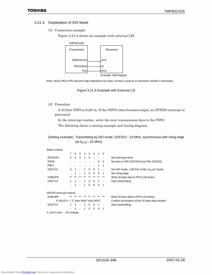
TMP92CA25
2007-02-28 92CA25-348
3.21.4 Explanation of SIO Mode
(1) Connection example Figure 3.21.6 shows an example with external LSI.
Note: Since P90 to P91 become high impedance by reset, connect a pull-up or pull-down resistor if necessary.
Figure 3.21.6 Example with External LSI
(2) Procedure A 32-byte FIFO is built-in. If the FIFO’s data becomes empty, an INTI2S interrupt is
generated. In the interrupt routine, write the next transmission data to the FIFO. The following shows a setting example and timing diagram.
(Setting example) Transmitting by SIO mode, I2SCKO = 10 MHz, synchronous with rising edge (at fSYS = 20 MHz)
(Main routine) 7 6 5 4 3 2 1 0 INTE5I2S X 0 0 1 X − − − Set interrupts level. P9CR − − − − − − 0 0 Set pins to P90 (I2SCKO) and P91 (I2SDO). P9FC − − − − − − 1 1 I2SCTL0 0 1 − 1 0 0 1 − Set SIO mode, LSB first, 8 bits, fSYS/2 clocks. − 1 − 1 0 0 0 1 Set rising edge. I2SBUFR ** ** ** ** ** ** ** ** Write 32-byte data to FIFO (16 times). I2SCTL0 1 1 − 1 0 0 1 − Start transmitting. − 1 − 1 0 0 0 1
(INTI2S interrupt routine) I2SBUFR ** ** ** ** ** ** ** ** Write 32-byte data to FIFO (16 times).
If <BUSY> = “1” then WAIT else NEXT Confirm termination of the 32-byte data transfer. I2SCTL0 1 1 − 1 0 0 1 − Start transmitting. − 1 − 1 0 0 0 1
X: Don't care, −: No change
(Transmitter)
P90/I2SCKO
P91/I2SDO
Port
(Receiver) SCK SI
RCK
TMP92CA25
Example: Shift register
Downloaded from Elcodis.com electronic components distributor
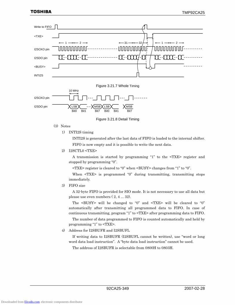
TMP92CA25
2007-02-28 92CA25-349
Figure 3.21.7 Whole Timing
Figure 3.21.8 Detail Timing
(3) Notes 1) INTI2S timing
INTI2S is generated after the last data of FIFO is loaded to the internal shifter. FIFO is now empty and it is possible to write the next data.
2) I2SCTL0 <TXE> A transmission is started by programming “1” to the <TXE> register and
stopped by programming “0”. <TXE> register is cleared to “0” when <BUSY> changes from “1” to “0”. When <TXE> is programmed “0” during transmitting, transmitting stops
immediately. 3) FIFO size
A 32-byte FIFO is provided for SIO mode. It is not necessary to use all data but please use even numbers ( 2, 4 ... 32).
The <BUSY> will be changed to “0” and <TXE> will be cleared to “0” automatically after transmitting all programmed data to FIFO. In case of continuous transmitting, program “1” to <TXE> after programming data to FIFO.
The number of data programmed to FIFO is counted automatically and held by programming “1” to <TXE>.
4) Address for I2SBUFR and I2SBUFL If writing data to I2SBUFR (I2SBUFL cannot be written), use “word or long
word data load instruction”. A “byte data load instruction” cannot be used. The address of I2SBUFR is selectable from 0800H to 0803H.
I2SCKO pin
I2SDO pin LSB Bit0 Bit1
10 MHz
MSBBit7 Bit0
LSBBit1 Bit7
MSB
Write to FIFO
<TXE>
INTI2S
<BUSY>
I2SDO pin
I2SCKO pin
1 2 31 32 1 2
Downloaded from Elcodis.com electronic components distributor

TMP92CA25
2007-02-28 92CA25-350
3.22 Power Supply Backup (Power Supply Backup)
TMP92CA25 includes three type power supply systems. Analog Power supply input (AVCC - AVSS) Digital Power suppy input (DVCC - DVSS) Power supply input for RTC (RTCVCC - DVSS)
Each Power supply is independent.
Figure 3.22.1 Power supply input system
Figure 3.22.2 Outside circuit example for PSB
XT2 XT1 BEDVSS1∼DVSS4AVSS
CPU control
& Other logic
ADC control
RTC control
High-OSC
Low-OSC
AVCC DVCC1∼DVCC3 RTCVCC TMP92CA25
Port M
PM1(MLDALM)
PM2( ALARM , MLDALM )
BE
RTC
32K_OSC
TMP92CA25 Sub battery for RTC
Main power suorce &
Other device
DVCC RTCVCC
DVSS
Downloaded from Elcodis.com electronic components distributor
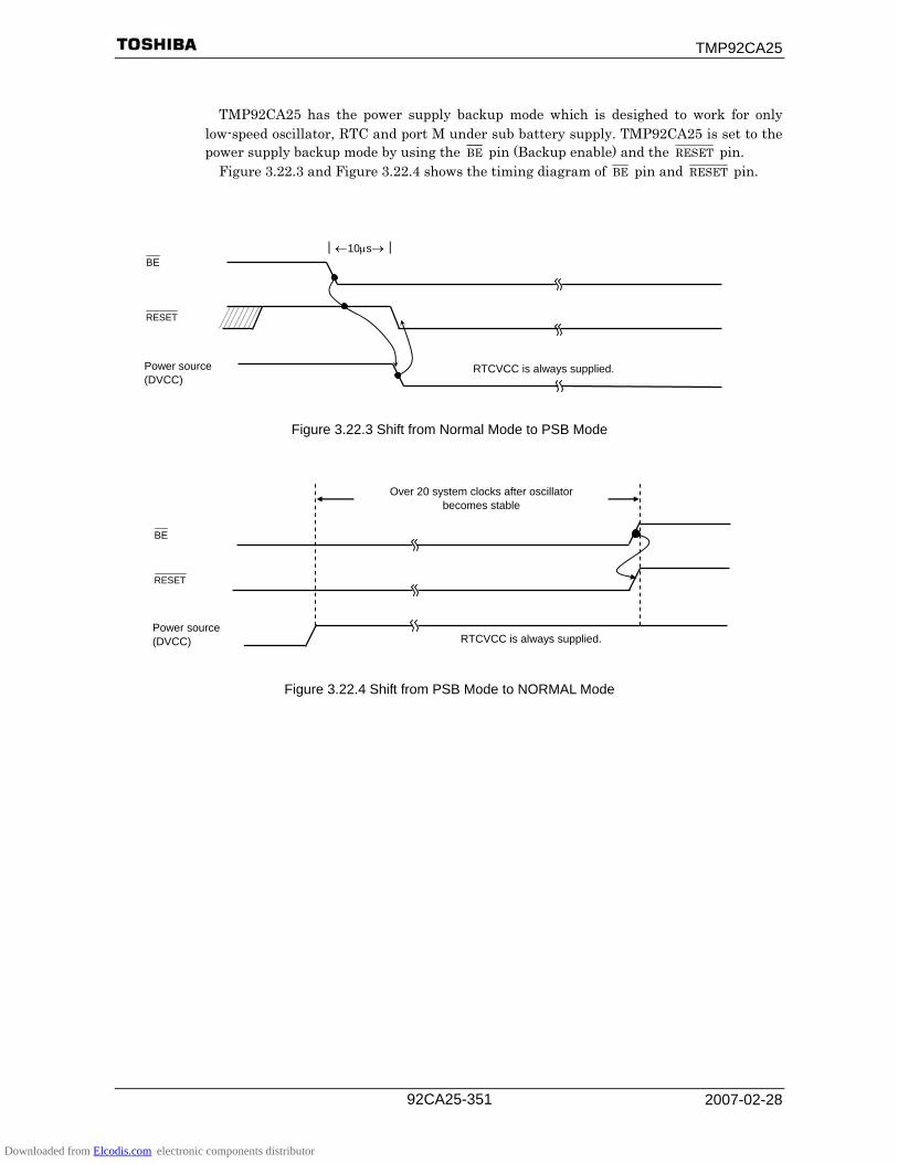
TMP92CA25
2007-02-28 92CA25-351
TMP92CA25 has the power supply backup mode which is desighed to work for only
low-speed oscillator, RTC and port M under sub battery supply. TMP92CA25 is set to the power supply backup mode by using the BE pin (Backup enable) and the RESET pin.
Figure 3.22.3 and Figure 3.22.4 shows the timing diagram of BE pin and RESET pin.
Figure 3.22.3 Shift from Normal Mode to PSB Mode
Figure 3.22.4 Shift from PSB Mode to NORMAL Mode
RESET
Power source (DVCC)
BE
RTCVCC is always supplied.
Over 20 system clocks after oscillator becomes stable
RESET
Power source (DVCC)
RTCVCC is always supplied.
|←10μs→| BE
Downloaded from Elcodis.com electronic components distributor
TMP92CA25
2007-02-28 92CA25-352
Backup enable pin ( BE ) Low frequency oscillator, RTC and Port M can work also if BE = “L”. If BE = “L”, Low frequency oscillator, RTC and Port Mare separated from CPU and
so on in internal. Therefore, it is prohibited accessing to RTC register and Port M. In addition, Low frequency oscillator (fs) isn’t provided except RTC circuit (Melody Alarm generator etc.). So, ALARM (= output function of RTC) can output from PM2 pin, if port is set before set to BE = “L”.
Note:
1: If “H” level signal was inputted to general purpose port with power off condition, current is used more than always. Therefore, set to “l” level or High-impedance condition. If this back up function is used, set BE pin to “L” level when DVCC power off.
2: When BE pin is set to “L”, Low frequency oscillator operation become same with EMCCR0<DRVOSCL> = “0”, forcibly. Therefore, don’t set to BE = “L”, when it is not operated Low frequency oscillator.
3: When BE pin is set to “L”, PM2, PM1 pins condition change according to setting value of PMDR<PM2D, PM1D>. If keep output PM2, PM1 pins write “11” to <PM2D, PM1D> before set to BE = “L”.
4: If release RESET , release RESET after BE = “H”.
Downloaded from Elcodis.com electronic components distributor

TMP92CA25
2007-02-28 92CA25-353
3.23 External bus release function
TMP92CA25 have external bus release function that can connect bus master to external. Bus release request ( BUSRQ ), bus release answer ( BUSAK ) pin is assigned to Port L6 and L7. And, it become effective by setting to PLCR and PLFC. Figure 3.23.1 shows operation timing. Time that from BUSRQ pin inputted “0” until
busis released ( BUSAK is set to “0”) depend on instruction that CPU execute at that time.
Figure 3.23.1 Bus release function operation timing
3.23.1 Non release pin
If it received bus release request, CPU release bus to external by setting BUSAK pin to “0” without start next bus. In this case, pin that is released have 3 types (A, B and C). Eve operation that set to high impedance (HZ) is different in 3 types. Table 3.23.1 shows support pin for 3 types. Any pin become non release pin only case of setting to that function by setting port. Therefore, if pin set to output port and so on, it is not set non relase pin, and it hold previous condition.
Table 3.23.1 Non release pin
Type Eve operation that set to HZ
Support function (Pin name)
A Drive “1” A23-A16(P67-P60), A15-A0, RD (P70), WRLL (P71), WRLU (P72), EA24(P73), EA25(P74), R/ W (P75),
0CS (P80), 1CS (P81), SDCS (P81), 2CS (P82), CSZA (P82), 3CS (P83),
CSZB (P84), CSZC (P85), CSZD (P86), CSZE (P87), EA24(PC6), EA25(PC7), CSZF (PC7), SRLLB , SDRAS (PJ0), SRLUB , SDCAS (PJ1), SRWR , SDWE (PJ2), SDCLK(PF7), SDLLDQM(PJ3), SDLUDQM(PJ4)
B Drive “0” SDCKE(PJ7) C None operation D15-D8(P17-P10), D7-D0
fSYS
BUSRQ (PL6)
BUSAK (PL7)
External bus pin (A type)
External bus pin(B type)
External bus pin (C type)
External bus release cycle
Downloaded from Elcodis.com electronic components distributor

TMP92CA25
2007-02-28 92CA25-354
3.23.2 Connection example
Figure 3.23.2 show connection example.
Figure 3.23.2 Connection example
3.23.3 Note
If use bus release function, be careful following notes.
1) Prohibit using this function together LCD controller and, SDRAM controller If use this function, prohibit use LCD controller in SR mode. And,
prohibitalso SDRAMC basically, but if external bus master use SDRAM, set SDRAM to SR (self refresh) condition before bus release request. And, when finish bus release, release SR condition. In this case, confirm each condition by handshake of general purpose port.
2) Support standby mode The condition that can receive this function is only CPU operationg
condition and during IDLE2 mode. During IDLE1 and STOP condition don’t receive. (Bus release function is ignored).
3) Internal resource access disable External bus master cannnot access to internal memory and interhal I/O
of TMP92CA25. Internal I/O operation during bus releasing. 4) Internal I/O operation during bus releasing
Internal I/O continue operation during bus releasing, please be careful. And, if set the watchdog timer, set runaway time by consider bus release time.
5) Non release pin Control output pin for NAND-Flash ( CE0ND , CE1ND , NDALE, NDCLE,
NDRE , NDWE ) are not non release pins.
CLE ALE
TMP92CA25
CLE ALE
BUSRQBUSAK
External bus pin (A type)
External bus pin (B type)
External bus pin (C type)
Memory
External bus master
Downloaded from Elcodis.com electronic components distributor

TMP92CA25
2007-02-28 92CA25-355
4. Electrical Characteristics
4.1 Absolute Maximum Ratings
Parameter Symbol Rating Unit Power Supply Voltage VCC −0.5 to 4.0 V Input Voltage VIN −0.5 to VCC + 0.5 V Output Current IOL 2 mA Output Current (MX, MY pin) IOL 15 mA Output Current IOH −2 mA Output Current (PX, PY pin) IOH −15 mA Output Current (Total) Σ IOL 80 mA Output Current (Total) Σ IOH −80 mA Power Dissipation (Ta = 85°C) PD 600 mW Soldering Temperature (10 s) TSOLDER 260 °C Storage Temperature TSTG −65 to 150 °C Operation Temperature TOPR −20 to 70 °C
Note: The Absolute maximum ratings are rated values which must not be exceeded during operation, even for an instant. Any one of the ratings must not be exceeded. If any absolute maximum rating is exceeded, the device may break down or its performance may be degraded, causing it to catch fire or explode resulting in injury to the user. Thus, when designing products which include this device, ensure that no absolute maximum rating value will ever be exceeded.
Solderability of lead free products
Test parameter Test condition Note
(1) Use of Sn-37Pb solder Bath Solder bath temperature = 230°C, Dipping time = 5 seconds The number of times = one, Use of R-type flux
Solderability
(2) Use of Sn-3.0Ag-0.5Cu solder bath Solder bath temperature = 245°C, Dipping time = 5 seconds The number of times = one, Use of R-type flux (use of lead-free)
Pass: solderability rate until forming ≥ 95%
Downloaded from Elcodis.com electronic components distributor

TMP92CA25
2007-02-28 92CA25-356
4.2 DC Electrical Characteristics (1/2)
VCC = 3.3 ± 0.3V/X1 = 6 to 40 MHz/Ta = −20 to 70°C VCC = 2.7 − 3.6V/X1 = 6 to 27 MHz/Ta = −20 to 70°C
Parameter Symbol Min Typ. Max Unit Condition 3.0 X1 = 6 to 40 MHz Power supply voltage
(DVCC = AVCC) (DVSS = AVSS = 0 V)
VCC 2.7
3.6 V X1 = 6 to 27 MHz
XT1 = 30 to 34 kHz
Input low voltage for D0 to D7 P10 to P17 (D8 to D15)
VIL0 0.6
Input low voltage for P40 to P47, P50 to P57, P60 to P67, P71 to P76, P90, P93 to P94, PC4 to PC7, PF3 to PF6, PG0 to PG3, PJ5 to PJ6, PK4 to PK7, PL4 to PL7
VIL1 0.3 × VCC
Input low voltage for P91 to P92, P96 to P97, PA0 to PA7, PC0 to PC3, PF0 to PF2, BE , RESET
VIL2 0.25 × VCC
Input low voltage for AM0 to AM1 VIL3 0.3
Input low voltage for X1, XT1 VIL4
−0.3
0.2 × VCC
V
Input high voltage for D0 to D7 P10 to P17 (D8 to D15)
VIH0 2.0
Input high voltage for P40 to P47, P50 to P57, P60 to P67, P71 to P76, P90, P93 to P94, PC4 to PC7, PF3 to PF6, PG0 to PG3, PJ5 to PJ6, PK4 to PK7, PL4 to PL7
VIH1 0.7 × VCC
Input high voltage for P91 to P92, P96 to P97, PA0 to PA7, PC0 to PC3, PF0 to PF2, BE , RESET
VIH2 0.75 × VCC
Input high voltage for AM0 to AM1 VIH3 VCC − 0.3
Input high voltage for X1, XT1 VIH4 0.8 × VCC
VCC + 0.3 V
Downloaded from Elcodis.com electronic components distributor

TMP92CA25
2007-02-28 92CA25-357
DC Electrical Characteristics (2/2) Parameter Symbol Min Typ. Max Unit Condition
Output low voltage VOL 0.45 IOL = 1.6 mA VOH1 2.4 IOH = −400 μA
Output high voltage VOH2 0.9 × VCC
V
IOH = −20 μA Internal resistor (ON) MX, MY pins IMon 30 VOL = 0.2V
Internal resistor (ON) PX, PY pins IMon 30
Ω VOH = VCC −0.2V
VCC = 3.0 to 3.6 V
Input leakage current ILI 0.02 ±5 μA 0.0 ≤ VIN ≤ VCC Output leakage current ILO 0.05 ±10 μA 0.2 ≤ VIN ≤ VCC − 0.2 V Power down voltage at STOP (for internal RAM backup) VSTOP 1.8 3.6 V VIL2 = 0.2 × VCC,
VIH2 = 0.8 × VCC Pull-up resistor for RESET , PA0 to PA7 RRST
Programmable pull down resistor for p96
RKH 80 500 kΩ
Pin capacitance CIO 10 pF fc = 1 MHz Schmitt width for P91 to P92, P96 to P97, PA0 to PA7,PC0 to PC3, PF0 to PF2, BE , RESET
VTH 0.4 1.0 V
NORMAL (Note 2) 42 65 IDLE2 13 26 IDLE1 3.1 8.7
mA VCC = 3.6 V, fc = 40 MHz
110 Ta ≤ 70°C SLOW (Note 2) 41
70 Ta ≤ 50°C 80 Ta ≤ 70°C
IDLE2 15 30 Ta ≤ 50°C 60 Ta ≤ 70°C
IDLE1 4 20 Ta ≤ 50°C
VCC = 3.6 V, fs = 32 kHz
50 Ta ≤ 70°C STOP
ICC
0.2 15
μA
Ta ≤ 50°C VCC = 3.6 V
Note 1: Typical values are for when Ta = 25°C and VCC = 3.3 V unless otherwise noted.
Note 2: ICC measurement conditions (NORMAL, SLOW):
All functions are operational; output pins except the bus pin are opened, and input pins are fixed.
Bus pin CL = 30 pF
Downloaded from Elcodis.com electronic components distributor

TMP92CA25
2007-02-28 92CA25-358
4.3 AC Characteristics
4.3.1 Basic Bus Cycle
Read cycle Variable
No. Parameter SymbolMin Max
40 MHz 36 MHz 27 MHz Unit
1 OSC period (X1/X2) tOSC 25 166.7 25 27.7 37.0 2 System clock period ( = T) tCYC 50 333.3 50 55.5 74.0 3 SDCLK low width tCL 0.5 T − 15 10 12.7 22 4 SDCLK high width tCH 0.5 T − 15 10 12.7 22
tAD (3.0 V) 2.0 T − 30 70 81 − 5-1 A0 to A23 valid → D0 to D15
Input at 0 waits tAD (2.7 V) 2.0 T − 35 − − 113 tAD3 (3.0 V) 3.0 T − 30 120 136.5 −
5-2 A0 to A23 valid → D0 to D15 Input at 1 wait tAD3 (2.7 V) 3.0 T − 35 − − 187
tRD(a) 1.5 T − 30 45 53.3 81 tRD(b) 1.25 T − 30 32.5 39.5 62.5 6-1 RD falling → D0 to D15
Input at 0 waits tRD(c) 1.0 T − 30 20 25.7 44 tRD3(a) 2.5 T − 30 95 108.8 155 tRD3(b) 2.25 T − 30 82.5 95 136.5 6-2 RD falling → D0 to D15
Input at 1 wait tRD3(c) 2.0T − 30 70 312 118 tRR(a) 1.5 T − 20 55 63.2 91 tRR(b) 1.25 T − 20 42.5 49.4 72.5 7-1 RD low width at 0 waits tRR(c) 1.0 T − 20 30 35.6 54 tRR3(a) 2.5 T − 20 105 118.8 165 tRR3(b) 2.25 T − 20 92.5 105 146.5 7-2 RD low width at 1 wait tRR3(c) 2.0 T − 20 80 91.2 128 tAR(a) 0.5 T − 20 5 7.7 17 tAR(a) 0.75 T − 20 17.5 21.5 35.5 8 A0 to A23 valid → RD falling tAR(a) 1.0 T − 20 30 35.3 54 tRK(a) 0.5 T − 20 5 7.7 17 tRK(b) 0.25 T − 20 −7.5 −6.1 −1.5 9 RD falling → SDCLK rising tRK(c) 0 T − 20 −20 −20 −20
10 A0 to A23 valid → D0 to D15 hold tHA 0 0 0 0 11 RD rising → D0 to D15 hold tHR 0 0 0 0 12 WAIT setup time tTK 15 15 15 15 13 WAIT hold time tKT 5 5 5 5
14 Data byte control access time for SRAM tSBA 1.5 T − 30 45 53.3 81
tRRH(a) 0.5 T − 15 10 12.7 22 tRRH(b) 0.75 T − 15 22.5 26.5 40.5 15 RD high width tRRH(c) 1.0 T − 15 35 40.3 59
ns
AC measuring condition
• Output: High = 0.7 VCC, Low = 0.3 VCC, CL = 50 pF
• Input: High = 0.9 VCC, Low = 0.1 VCC
Note1: The figures in the “Variable” column cover the whole VCC range (2.7 V to 3.6 V). Exceptions are shown by the VCC (min), “(3.0 V)” or “(2.7 V)”, added to the “Symbol” column.
Note2: The figures in the (a), (b) and (c) of “Symbol” column shows difference of falling timing of RD pin. Falling timing of RD pin is set by MEMECR0<RDTMG1:0>. If MEMCR0<RDTMG1:0> is “00”, it correspond with (a) in above table, and “01” is (b), “10” is (c).
Downloaded from Elcodis.com electronic components distributor

TMP92CA25
2007-02-28 92CA25-359
Write cycle Variable
No. Parameter SymbolMin Max
40 MHz 36 MHz 27 MHz Unit
16-1 D0 to D15 valid → WRxx rising at 0 waits tDW 1.25T − 35 27.5 34.3 57.5
16-2 D0 to D15 valid → WRxx rising at 1 wait tDW3 2.25T − 35 77.5 89.8 131.5
17-1 WRxx low width at 0 waits tWW 1.25T − 30 32.5 34.3 62.5 17-2 WRxx low width at 1 wait tWW3 2.25T − 30 82.5 89.8 136.5
18 A0 to A23 valid → WR falling tAW 0.5T − 20 5 7.7 17 19 WRxx falling → SDCLK rising tWK 0.5T − 20 5 7.7 17 20 WRxx rising → A0 to A23 hold tWA 0.25T − 5 7.5 8.8 13.5 21 WRxx rising → D0 to D15 hold tWD 0.25T − 5 7.5 8.8 13.5
tRDO (3.0 V) 0.5T − 5 20 22.7 − 22 RD rising → D0 to D15 output
tRDO (2.7 V) 0.5T − 7 − − 30 23 Write pulse width for SRAM tSWP 1.25T − 30 32.5 39.3 62.5
24 Data byte control to end of write for SRAM tSBW 1.25T − 30 32.5 39.3 62.5
25 Address setup time for SRAM tSAS 0.5T − 20 5 7.7 17 26 Write recovery time for SRAM tSWR 0.25T − 5 7.5 8.8 13.5 27 Data setup time for SRAM tSDS 1.25T − 35 27.5 34.3 57.5 28 Data hold time for SRAM tSDH 0.25T − 5 7.5 8.8 13.5
ns
AC measuring condition
• Output: High = 0.7 VCC, Low = 0.3 VCC, CL = 50 pF
• Input: High = 0.9 VCC, Low = 0.1 VCC
Note: The figures in the “Variable” column cover the whole VCC range (2.7 V to 3.6 V). Exceptions are shown by the VCC (min), “(3.0 V)” or “(2.7 V)”, added to the “Symbol” column.
Downloaded from Elcodis.com electronic components distributor
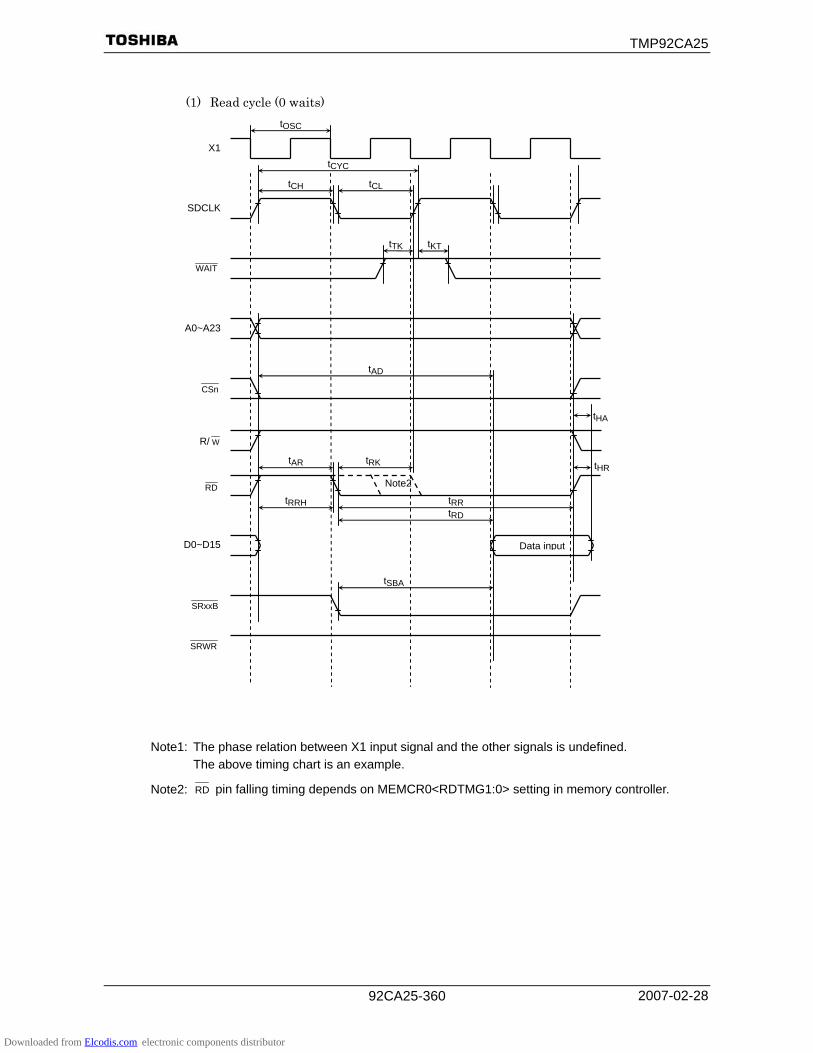
TMP92CA25
2007-02-28 92CA25-360
(1) Read cycle (0 waits)
Note1: The phase relation between X1 input signal and the other signals is undefined. The above timing chart is an example.
Note2: RD pin falling timing depends on MEMCR0<RDTMG1:0> setting in memory controller.
tOSC
SDCLK
WAIT
A0~A23
D0~D15
SRxxB
X1
CSn
RD
SRWR
tCH
tCYC
tCL
tTK tKT
tAD
tRRtRD
tRRH
tAR tRK
tSBA
Data input
tHA
tHR
R/ W
Note2
Downloaded from Elcodis.com electronic components distributor

TMP92CA25
2007-02-28 92CA25-361
(2) Write cycle (0 waits)
Note: The phase relation between X1 input signal and the other signals is undefined. The above timing chart is an example.
tOSC
SDCLK
WAIT
A0~A23
D0~D15
SRxxB
X1
CSn
WRxx
SRWR
tCH
tCYC
tCL
tTK tKT
tWWtDW
tAW tWK
tSBW
Data output
tWA
tSWR tWD
RD
tRDO
tSDH
tSAS tSWP
tSDS
R/ W
Downloaded from Elcodis.com electronic components distributor

TMP92CA25
2007-02-28 92CA25-362
(3) Read cycle (1 wait)
(4) Write cycle (1 wait)
SDCLK
Data output
tWW3tDW3
WAIT
A0 to A23
CSn
WRxx
D0 to D15
RD
R/ W
SDCLK
Data input
tRR3
tAD3
tRD3
WAIT
A0 to A23
CSn
RD
D0 to D15
R/ W
Downloaded from Elcodis.com electronic components distributor

TMP92CA25
2007-02-28 92CA25-363
4.3.2 Page ROM Read Cycle
(1) 3-2-2-2 mode
Variable No. Parameter Symbol
Min Max 40 MHz 36 MHz 27 MHz Unit
1 System clock period ( = T) tCYC 50 166.7 50 55.5 74 2 A0, A1 → D0 to D15 input tAD2 2.0T − 50 50 61 98 3 A2 to A23 → D0 to D15 input tAD3 3.0T − 50 100 116.5 172
tRD3(a) 2.5T − 45 80 93.8 140 tRD3(b) 2.25T − 45 67.5 79.6 121.5 4 RD falling → D0 to D15 input tRD3(c) 2.0T − 45 55 66 103
5 A0 to A23 Invalid → D0 to D15 hold tHA 0 0 0 0 6 RD rising → D0 to D15 hold tHR 0 0 0 0
ns
AC measuring condition • Output: High = 0.7 VCC, Low = 0.3 VCC, CL = 50 pF
• Input: High = 0.9 VCC, Low = 0.1 VCC
Note: The figures in the (a), (b) and (c) of “Symbol” column shows difference of falling timing of RD pin. Falling timing of RD pin is set by MEMECR0<RDTMG1:0>. If MEMCR0<RDTMG1:0> is “00”, it correspond with (a) in above table, and “01” is (b), “10” is (c).
Timing pulse (8-byte setting)
SDCLK
A0 to A23
2CS
RD
D0 to D15
+0 +1 +2 +3
Data input
Datainput
Data input
Data input
tAD3 tAD2 tAD2 tAD2 tHA
tHR tRD3 tHA tHAtHA
tCYC
Downloaded from Elcodis.com electronic components distributor
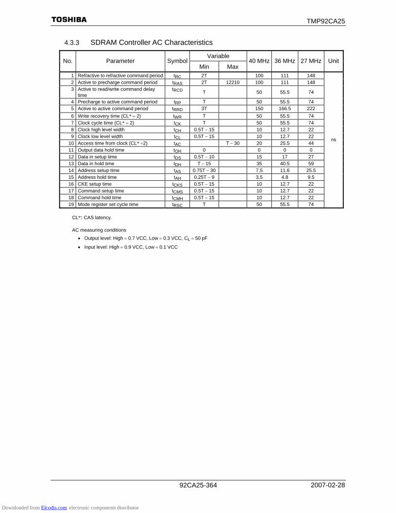
TMP92CA25
2007-02-28 92CA25-364
4.3.3 SDRAM Controller AC Characteristics
Variable No. Parameter Symbol
Min Max 40 MHz 36 MHz 27 MHz Unit
1 Ref/active to ref/active command period tRC 2T 100 111 148 2 Active to precharge command period tRAS 2T 12210 100 111 148 3 Active to read/write command delay
time tRCD T 50 55.5 74
4 Precharge to active command period tRP T 50 55.5 74 5 Active to active command period tRRD 3T 150 166.5 222 6 Write recovery time (CL* = 2) tWR T 50 55.5 74 7 Clock cycle time (CL* = 2) tCK T 50 55.5 74 8 Clock high level width tCH 0.5T − 15 10 12.7 22 9 Clock low level width tCL 0.5T − 15 10 12.7 22
10 Access time from clock (CL* =2) tAC T − 30 20 25.5 44 11 Output data hold time tOH 0 0 0 0 12 Data in setup time tDS 0.5T − 10 15 17 27 13 Data in hold time tDH T − 15 35 40.5 59 14 Address setup time tAS 0.75T − 30 7.5 11.6 25.5 15 Address hold time tAH 0.25T − 9 3.5 4.8 9.5 16 CKE setup time tCKS 0.5T − 15 10 12.7 22 17 Command setup time tCMS 0.5T − 15 10 12.7 22 18 Command hold time tCMH 0.5T − 15 10 12.7 22 19 Mode register set cycle time tRSC T 50 55.5 74
ns
CL*: CAS latency.
AC measuring conditions • Output level: High = 0.7 VCC, Low = 0.3 VCC, CL = 50 pF
• Input level: High = 0.9 VCC, Low = 0.1 VCC
Downloaded from Elcodis.com electronic components distributor

TMP92CA25
2007-02-28 92CA25-365
(1) SDRAM read timing (CPU access or LCDC normal access)
SDCLK
SDxxDQM
SDCS
SDRAS
SDCAS
SDWE
tCH tCL
tCK
tRCDtRP tRAS tRP
tCMS tCMHtCMS
tCMH
tRRD
Column Row A1 to A10
D0 to D15
16-bit data bus
A11
A12 to A15
tAHtAS
tAS tAH
Column Row
Column Row
Data input
tAC tOH
Downloaded from Elcodis.com electronic components distributor

TMP92CA25
2007-02-28 92CA25-366
(2) SDRAM write timing (CPU access)
SDCLK
SDxxDQM
SDCS
SDRAS
SDCAS
SDWE
tCH tCL
tCK
tWRtRP tRCD tRPtCMS
tRRDtCMS
tCMH
tRAS
tCMH
Column Row A1 to A12
D0 to D15
16-bit data bus
A11
A12 to A15
tAHtAS
tAS tAH
Column Row
Column Row
Data output
tDS tDH
Downloaded from Elcodis.com electronic components distributor
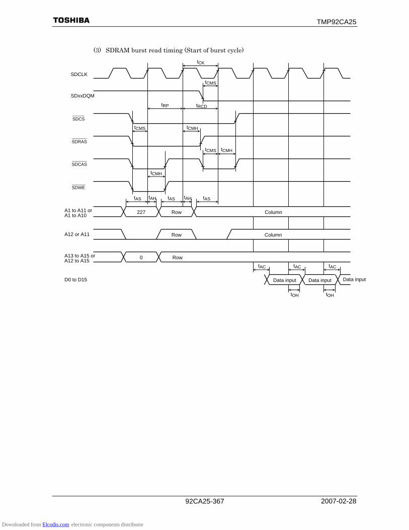
TMP92CA25
2007-02-28 92CA25-367
(3) SDRAM burst read timing (Start of burst cycle)
Column Row
SDCLK
SDxxDQM
SDCS
SDRAS
SDCAS
A1 to A11 or A1 to A10
D0 to D15
SDWE
A12 or A11
A13 to A15 or A12 to A15
tCK
tRCDtRP
tCMS tCMH
tCMH
tAHtAS
Column Row
Row
Data input
tAC
tCMH
tCMS
tCMS
227
tAH tAS tAS
0 tAC tAC
Data input Data input
tOH tOH
Downloaded from Elcodis.com electronic components distributor

TMP92CA25
2007-02-28 92CA25-368
(4) SDRAM burst read timing (End of burst cycle)
Column
Column 220
SDCLK
SDxxDQM
SDCS
SDRAS
SDCAS
A1 to A11 or A1 to A10
D0 to D15
SDWE
A12 or A11
A13 to A15 or A12 to A15
tCK
tRCtRSC
tCMS
tCMH
Column
Data input
tCMH
tCMS
tCMS
Column
tAS
tAC tAC
Data input
tOH tOH
tCMH
Column 0 Row
Data input
tOH
Downloaded from Elcodis.com electronic components distributor

TMP92CA25
2007-02-28 92CA25-369
(5) SDRAM initialize timing
220
SDCLK
SDxxDQM
SDCS
SDRAS
SDCAS
A1 to A12
SDWE
A20 to A23 (BS0 and BS1)
tCH tCL
tCK
tRSC tRC
tCMS tCMH
tCMS
tCMH
tAHtAS
tCMH
tCMS
tAS
Downloaded from Elcodis.com electronic components distributor

TMP92CA25
2007-02-28 92CA25-370
(6) SDRAM refresh timing
(7) SDRAM self refresh timing
SDCLK
SDxxDQM
SDCS
SDRAS
SDCAS
SDWE
tCK
tRC tRC
tCMHtCMS
SDCLK
SDCKE
SDCS
SDRAS
SDCAS
SDWE
tCK
tRC
tCMH tCMS
tCKS tCKS
SDxxDQM
Downloaded from Elcodis.com electronic components distributor

TMP92CA25
2007-02-28 92CA25-371
4.3.4 NAND Flash Controller AC Characteristics
Variable No. Parameter Symbol
Min Max 40 MHz 36 MHz 27 MHz Unit
1 NDRE low width tRP (1 + n) T − 12 38 43.5 62 tREA (3.0 V) (1 + n) T − 25 25 30.5 − 2
NDRE data access time tREA (2.7 V) (1 + n) T − 30 − − 44
3 Read data hold time tOH 0 0 0 0 4 NDWE low width tWP (0.75 + n) T − 20 17.5 21.6 35.5 5 Write data setup time tDS (3.25 + n) T − 30 132.5 150.3 210.5 6 Write data hold time tDH 0.25 T − 2 10.5 11.8 16.5
ns
AC measuring conditions • Output level: High = 0.7 VCC, Low = 0.3 VCC, CL = 50 pF
• Input level: High = 0.9 VCC, Low = 0.1 VCC
Note 1: The “n” shown in “Variable” refers to the wait number which is set to NDnFSPR<SPW3:0> register.
Example: When NDnFSPR<SPW3:0> = “0001”, tRP = (1 + n) T − 12 = 2T − 12
Note 2: The figures in the “Variable” column cover the whole VCC range (2.7 V to 3.6 V). Exceptions are shown by the VCC (min), “(3.0 V)” or “(2.7 V)”, added to the “Symbol” column.
Example: (3.0V) : VCC range = 3.0V to 3.6V
Data input
SDCLK
A0 to A23
NDRE
NDWE
D0 to D7
tRP
tREA
tOH
Read cycle
Data output
NDRE
NDWE
D0 to D7
tWP
tDH
Write cycle
tDS
Downloaded from Elcodis.com electronic components distributor

TMP92CA25
2007-02-28 92CA25-372
4.3.5 Serial Channel Timing
(1) SCLK input mode (I/O interface mode)
Variable Parameter Symbol
Min Max 40 MHz 36 MHz 27 MHz Unit
SCLK cycle tSCY 16T 0.8 0.888 1.184 μsOutput data → SCLK rising/falling tOSS tSCY/2 − 4T − 110 90 114 186 SCLK rising/falling → Output data hold tOHS tSCY/2 + 2T + 0 500 554 740 SCLK rising/falling → Input data hold tHSR 3 T + 10 160 175 232 SCLK rising/falling → Input data valid tSRD tSCY − 0 800 888 1184 Input data valid → SCLK rising/falling tRDS 0 0 0 0
ns
(2) SCLK output mode (I/O Interface mode)
Variable Parameter Symbol
Min Max 40 MHz 36 MHz 27 MHz Unit
SCLK cycle (Programmable) tSCY 16 T 8192T 0.8 0.888 1.184 μsOutput data → SCLK rising/falling tOSS tSCY/2 − 40 360 404 552 SCLK rising/falling → Output data hold tOHS tSCY/2 − 40 360 404 552 SCLK rising/falling → Input data hold tHSR 0 0 0 0 SCLK rising/falling → Input data valid tSRD tSCY − 1T − 180 570 654 967 Input data valid → SCLK rising/falling tRDS 1 T + 180 230 233 253
ns
4.3.6 Interrupt Operation
Variable Parameter Symbol
Min Max 40 MHz 36 MHz 27 MHz Unit
INT0 to INT5 low width tINTAL 4 T + 40 240 262 336 INT0 to INT5 high width tINTAH 4 T + 40 240 262 336
ns
tSCY
0
SCLK Output mode/ input rising mode
SCLK (Input falling mode)
Output dataTXD 1 2 3
tOSS tOHS
Input dataRXD 0 1 2 3
tSRDtRDS
tHSR
Valid Valid Valid Valid
Downloaded from Elcodis.com electronic components distributor

TMP92CA25
2007-02-28 92CA25-373
4.3.7 LCD Controller (SR mode)
Variable Parameter Symbol
Min Max 40 MHz 36 MHz 27 MHz Unit
LCP0 clock period ( = tm) tCW 2 T 100 111 148 LCP0 high width tCWH 0.5 tm − 12 38 43.5 62 LCP0 low width tCWL 0.5 tm − 12 38 43.5 62 Data valid → LCP0 falling tDSU 0.5 tm − 20 30 35.5 54 LCP0 falling → Data hold tDHD 0.5 tm − 5 45 50.5 69
ns
4.3.8 I2S Timing (I2S, SIO Mode)
Variable Parameter Symbol
Min Max 40 MHz 36 MHz 27 MHz Unit
I2SCKO clock period tCR T 50 55 74 I2SCKO high width tHB 0.5 tCR − 15 10 12 22 I2SCKO low width tLB 0.5 tCR − 15 10 12 22 I2SDO, I2SWS setup time tSD 0.5 tCR − 15 10 12 22 I2SDO, I2SWS hold time tHD 0.5 tCR − 5 20 22 32
ns
AC measuring conditions • Output level: High = 0.7 VCC, Low = 0.3 VCC, CL = 10 pF
LCP0
tCWH tCWL
tCW
LD0 to LD7
tDHD tDSU
LD0 to LD7 output
I2SCKO
tCR tLB tHB
I2SDO
tHD tHDtSD
I2SWS
Downloaded from Elcodis.com electronic components distributor

TMP92CA25
2007-02-28 92CA25-374
4.3.9 SPI control Timing
Variable Parameter Symbol
Min Max 40 MHz 36 MHz 27 MHz Unit
SPCLK frequency (=1/S) tCR 20 20 18 13.5 MHzSPCLK rising time tHB 6 6 6 6 SPCLK falling time tLB 6 6 6 6 SPCLK Low pulse width tSD 0.5S −6 19 21 31 SPCLK High pulse width tHD 0.5S −13 12 14 24 Output data valid → SPCLK rise 0.5S −18 7 9 19 Output data valid → SPCLK fall 0.5S −21 4 6 16 SPCLK rise → Output data hold 0.5S −10 15 17 27 Input data valid → SPCLK rise 0S + 5 5 5 5 SPCLK rise → Input data hold 0S + 5 5 5 5
ns
AC measuring conditions • Output level: High = 0.7 VCC, Low = 0.3 VCC, CL = 25 pF
• Input level: High = 0.9 VCC, Low = 0.1 VCC
SPCLK output (When SPIMD<TCPOL,RCPOL> = “11”)
SPDO output
fPP
tr
tf
0.2VCC
0.7VCCtWL tWH
tODS tODH
tIDS tIDH
SPDI intput
SPCLK output (When SPIMD<TCPOL,RCPOL> = “00”)
Downloaded from Elcodis.com electronic components distributor
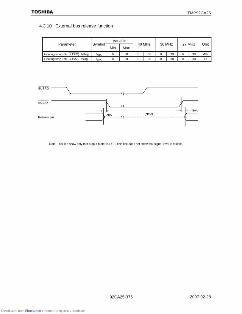
TMP92CA25
2007-02-28 92CA25-375
4.3.10 External bus release function
Note: This line show only that output buffer is OFF. This line does not show that signal level is middle.
Variable Parameter Symbol
Min Max40 MHz 36 MHz 27 MHz Unit
Floating time until BUSRQ falling tABA 0 30 0 30 0 30 0 30 MHzFloating time until BUSAK rising tBAA 0 30 0 30 0 30 0 30 ns
Release pin tABA
tBAA
(Note)
BUSRQ
BUSAK
Downloaded from Elcodis.com electronic components distributor
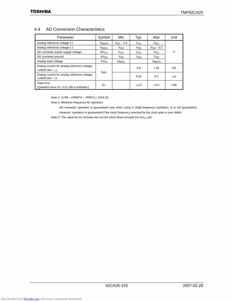
TMP92CA25
2007-02-28 92CA25-376
4.4 AD Conversion Characteristics
Parameter Symbol Min Typ. Max Unit Analog reference voltage (+) VREFH VCC − 0.2 VCC VCC Analog reference voltage (−) VREFL VSS VSS VSS + 0.2 AD converter power supply voltage AVCC VCC VCC VCC AD converter ground AVSS VSS VSS VSS Analog input voltage AVIN VREFL VREFH
V
Analog current for analog reference voltage <VREFON> = 1
0.8 1.35 mA
Analog current for analog reference voltage <VREFON> = 0
IREF 0.02 5.0 μA
Total error (Quantize error of ± 0.5 LSB is included.)
ET ±1.0 ±4.0 LSB
Note 1: 1LSB = (VREFH – VREFL) / 1024 [V]
Note 2: Minimum frequency for operation
AD converter operation is guaranteed only when using fc (high-frequency oscillator). fs is not guaranteed.
However, operation is guaranteed if the clock frequency selected by the clock gear is over 4MHz.
Note 3: The value for Icc includes the current which flows through the AVCC pin.
Downloaded from Elcodis.com electronic components distributor

TMP92CA25
2007-02-28 92CA25-377
4.5 Recommended Oscillation Circuit
The TMP92CA25 has been evaluated by the oscillator vender below. Use this information when selecting external parts.
Note: The total load value of the oscillator is the sum of external loads (C1 and C2) and the floating load of the actual assembled board. There is a possibility of operating error when using C1 and C2 values in the table below. When designing the board, design the minimum length pattern around the oscillator. We also recommend that oscillator evaluation be carried out using the actual board.
(1) Connection example
(2) Recommended ceramic oscillator: Murata Manufacturing Co., Ltd.
Note 1: The figure in parentheses ( ) under C1 and C2 is the built-in condenser type.
Note 2: The product numbers and specifications of the oscillators made by Murata Manufacturing Co., Ltd. are subject to change. For up-to-date information, please refer to the following URL:
http://www.murata.co.jp
Parameter of elements Running Condition
MCU
Oscillation
Frequency
[MHZ]
Oscillator Product Number C1
[pF]C2[pF]
Rf [Ω]
Rd[Ω]
Voltage of Power [V]
Ta [°C]
6.00 CSTCR6M00G55-R0 (39) (39)
10.00 CSTCE10M0G55-R0 (33) (33)TMP92CA25FG
20.00 CSTCE20M0V53-R0 (15) (15)
Open 0 2.7 ∼ 3.6 -20 ∼ +80
X1 X2
Rd
Rf
C2C1
High-frequency oscillator
XT1 XT2
Rd
C2C1
Low-frequency oscillator
Downloaded from Elcodis.com electronic components distributor

TMP92CA25
2007-02-28 92CA25-378
5. Table of Special function registers (SFRs) The SFRs include the I/O ports and peripheral control registers allocated to the 4-Kbyte address
space from 000000H to 001FFFH.
(1) I/O Port (11) UART/serial channel
(2) Interrupt control (12) SBI
(3) Memory controller (13) SPI controller
(4) MMU (14) AD converter
(5) Clock gear, PLL (15) Watchdog timer
(6) LCD controller (16) RTC (Real time clock)
(7) Touch screen I/F (17) Melody/alarm generator
(8) SDRAM controller (18) NAND flash controller
(9) 8-bit timer (19) I2S
(10) 16-bit timer
Table layout
Symbol Name Address 7 6 1 0
Bit symbol Read/Write Initial value after reset
Remarks
Note: “Prohibit RMW” in the table means that you cannot use RMW instructions on these register.
Example: When setting bit0 only of the register PxCR, the instruction “SET 0, (PxCR)” cannot be used. The LD (transfer)
instruction must be used to write all eight bits.
Read/Write R/W: Both read and write are possible. R: Only read is possible. W: Only write is possible. W*: Both read and write are possible (when this bit is read as “1”.) Prohibit RMW: Read-modify-write instructions are prohibited. (The EX, ADD, ADC,
BUS, SBC, INC, DEC, AND, OR, XOR, STCF, RES, SET, CHG, TSET, RLC, RRC, RL, RR, SLA, SRA, SLL, SRL, RLD and RRD instruction are read-modify-write instructions.)
R/W*: Read-modify-write is prohibited when controlling the pull-up resistor.
Downloaded from Elcodis.com electronic components distributor

TMP92CA25
2007-02-28 92CA25-379
Table 5.1 I/O Register Address Map
[1] Port Address Name Address Name Address Name Address Name
0000H 0010H 0020H P8 0030H PC
1H 1H 1H P8FC2 1H
2H 2H 2H 2H PCCR
3H 3H 3H P8FC 3H PCFC
4H P1 4H 4H P9 4H
5H 5H 5H P9FC2 5H
6H P1CR 6H 6H P9CR 6H
7H P1FC 7H 7H P9FC 7H
8H 8H P6 8H PA 8H
9H 9H 9H 9H
AH AH P6CR AH AH
BH BH P6FC BH PAFC BH
CH CH P7 CH CH PF
DH DH DH DH PFFC2
EH EH P7CR EH EH PFCR
FH
FH P7FC FH FH PFFC
Address Name Address Name Address Name Address Name
0040H PG 0050H PK 0080H 0090H PGDR
1H
1H 1H P1DR 1H
2H 2H PKCR 2H 2H 3H 3H PKFC 3H 3H PJDR 4H 4H PL 4H P4DR 4H PKDR 5H 5H 5H P5DR 5H PLDR 6H 6H PLCR 6H P6DR 6H PMDR 7H 7H PLFC 7H P7DR 7H PNDR 8H 8H PM 8H P8DR 8H 9H 9H 9H P9DR 9H AH AH AH PADR AH BH BH PMFC BH BH CH PJ CH PN CH PCDR CH DH DH DH DH EH PJCR EH PNCR EH EH FH PJFC FH PNFC FH PFDR FH
Note: Do not access un-named addresses.
Downloaded from Elcodis.com electronic components distributor

TMP92CA25
2007-02-28 92CA25-380
[2] INTC Address Name Address Name Address Name Address Name
00D0H INTE12
00E0H INTESPI 00F0H INTE0AD 0100H DMA0V 1H INTE34 1H INTESBI 1H INTETC01 1H DMA1V 2H 2H Reserved 2H INTETC23 2H DMA2V 3H 3H Reserved 3H INTETC45 3H DMA3V 4H INTETA01 4H Reserved 4H INTETC67 4H DMA4V 5H INTETA23 5H INTALM01 5H SIMC 5H DMA5V 6H 6H INTALM23 6H IIMC 6H DMA6V 7H 7H INTALM4 7H INTWDT 7H DMA7V 8H INTETB01 8H INTERTC 8H INTCLR 8H DMAB 9H 9H INTEKEY 9H 9H DMAR AH INTETBO0 AH INTELCD AH AH Reserved BH INTES0 BH INTE5I2S BH BH CH CH INTEND01 CH CH DH DH Reserved DH DH EH EH INTEP0 EH EH FH FH Reserved FH FH
[3] MEMC [4] MMU Address Name Address Name Address Name Address Name
0140H B0CSL
0150H 0160H 01D0H LOCALPX 1H B0CSH 1H 1H 1H LOCALPY 2H MAMR0 2H 2H 2H 3H MSAR0 3H 3H 3H LOCALPZ 4H B1CSL 4H 4H 4H LOCALLX 5H B1CSH 5H 5H 5H LOCALLY 6H MAMR1 6H 6H PMEMCR 6H 7H MSAR1 7H 7H 7H LOCALLZ 8H B2CSL 8H BEXCSL 8H MEMCR0 8H LOCALRX 9H B2CSH 9H BEXCSH 9H 9H LOCALRY AH MAMR2 AH AH AH BH MSAR2 BH BH BH LOCALRZ CH B3CSL CH CH CH LOCALWX DH B3CSH DH DH DH LOCALWY EH MAMR3 EH EH EH FH MSAR3 FH FH FH LOCALWZ
Note: Do not access un-named addresses.
Downloaded from Elcodis.com electronic components distributor

TMP92CA25
2007-02-28 92CA25-381
[5] CGEAR, PLL Address Name
10E0H SYSCR0
1H SYSCR1 2H SYSCR2 3H EMCCR0 4H EMCCR1 5H EMCCR2 6H Reserved 7H 8H PLLCR0 9H PLLCR1 AH BH CH DH EH FH
[6] LCDC Address Name Address Name
0840H LCDMODE0
0850H LSARAL 1H LCDFFP 1H LSARAM 2H LCDDVM 2H LSARAH 3H LCDSIZE 3H CMNAL 4H LCDCTL0 4H CMNAH 5H 5H 6H LCDSCC 6H LSARBL 7H 7H LSARBM 8H 8H LSARBH 9H 9H CMNBL AH AH CMNBH BH BH CH CH LSARCL DH DH LSARCM EH EH LSARCH FH FH
Note: Do not access un-named addresses.
Downloaded from Elcodis.com electronic components distributor

TMP92CA25
2007-02-28 92CA25-382
[7] TSI [8] SDRAMC [9] 8-bit timer [10] 16-bit timer Address Name Address Name Address Name Address Name
01F0H TSICR0
0250H SDACR1 1100H TA01RUN 1180H TB0RUN 1H TSICR1 1H SDACR2 1H 1H 2H 2H SDRCR 2H TA0REG 2H TB0MOD 3H 3H SDCMM 3H TA1REG 3H TB0FFCR 4H 4H 4H TA01MOD 4H 5H 5H 5H TA01FFCR 5H 6H 6H 6H 6H 7H 7H 7H 7H 8H 8H 8H TA23RUN 8H TB0RG0L 9H 9H 9H 9H TB0RG0H AH AH AH TA2REG AH TB0RG1L BH BH BH TA3REG BH TB0RG1H CH CH CH TA23MOD CH TB0CP0L DH DH DH TA3FFCR DH TB0CP0H EH EH EH EH TB0CP1L FH FH FH FH TB0CP1H
[11] SIO [12] SBI Address Name Address Name
1200H SC0BUF
1240H SBI0CR1 1H SC0CR 1H SBI0DBR 2H SC0MOD0 2H I2C0AR 3H BR0CR 3H SBI0CR2/SBI0SR4H BR0ADD 4H SBI0BR0 5H SC0MOD1 5H SBI0BR1 6H 6H 7H 7H 8H 8H 9H 9H AH AH BH BH CH CH DH DH EH EH FH FH
Note: Do not access un-named addresses.
Downloaded from Elcodis.com electronic components distributor

TMP92CA25
2007-02-28 92CA25-383
[13] SPI controller Address Name Address Name
0820H SPIMD
0830H SPITD 1H SPIMD 1H SPITD 2H SPICT 2H SPIRD 3H SPICT 3H SPIRD 4H SPIST 4H SPITS 5H SPIST 5H SPITS 6H SPICR 6H SPIRS 7H SPICR 7H SPIRS 8H SPIIS 8H 9H SPIIS 9H AH SPIWE AH BH SPIWE BH CH SPIIE CH DH SPIIE DH EH SPIIR EH FH SPIIR FH
Note: Do not access un-named addresses.
Downloaded from Elcodis.com electronic components distributor
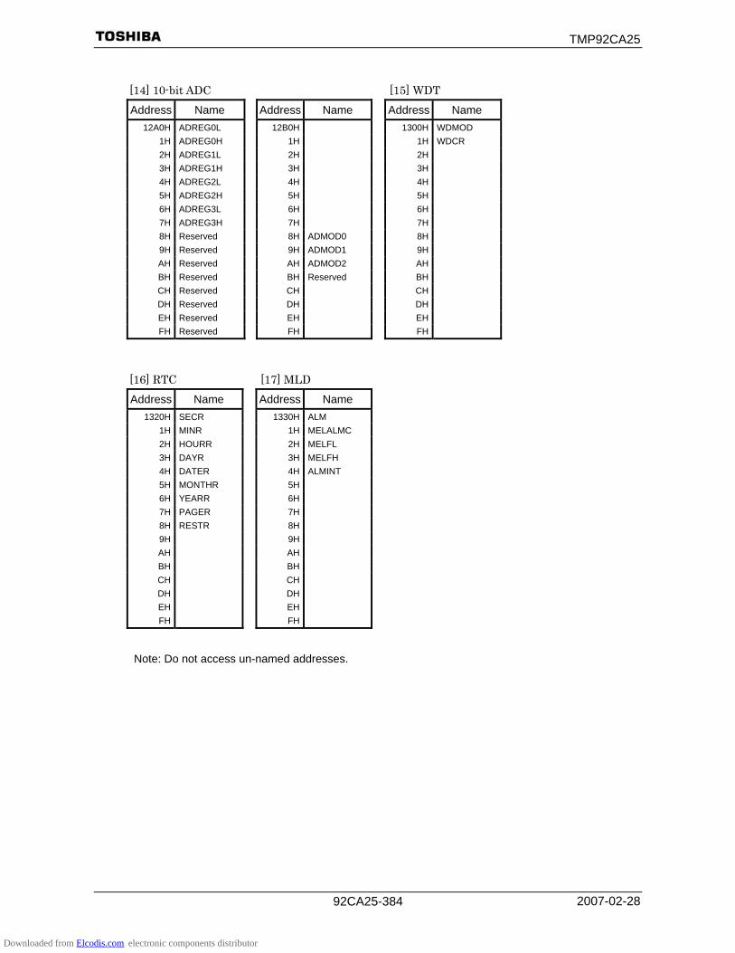
TMP92CA25
2007-02-28 92CA25-384
[14] 10-bit ADC [15] WDT Address Name Address Name Address Name
12A0H ADREG0L
12B0H 1300H WDMOD 1H ADREG0H 1H 1H WDCR 2H ADREG1L 2H 2H 3H ADREG1H 3H 3H 4H ADREG2L 4H 4H 5H ADREG2H 5H 5H 6H ADREG3L 6H 6H 7H ADREG3H 7H 7H 8H Reserved 8H ADMOD0 8H 9H Reserved 9H ADMOD1 9H AH Reserved AH ADMOD2 AH BH Reserved BH Reserved BH CH Reserved CH CH DH Reserved DH DH EH Reserved EH EH FH Reserved FH FH
[16] RTC [17] MLD Address Name Address Name
1320H SECR
1330H ALM 1H MINR 1H MELALMC 2H HOURR 2H MELFL 3H DAYR 3H MELFH 4H DATER 4H ALMINT 5H MONTHR 5H 6H YEARR 6H 7H PAGER 7H 8H RESTR 8H 9H 9H AH AH BH BH CH CH DH DH EH EH FH FH
Note: Do not access un-named addresses.
Downloaded from Elcodis.com electronic components distributor

TMP92CA25
2007-02-28 92CA25-385
[18] NAND flash controller Address Name Address Name Address Name Address Name
1CC0H
1CD0H ND0FIMR 1CE0H
1CF0H ND1FIMR 1H 1H 1H 1H 2H 2H 2H 2H 3H 3H 3H 3H 4H ND0FMCR 4H ND0FSPR 4H ND1FMCR 4H ND1FSPR 5H 5H 5H 5H 6H 6H 6H 6H 7H 7H 7H 7H 8H ND0FSR 8H ND0FRSTR 8H ND1FSR 8H ND1FRSTR 9H 9H 9H 9H AH AH AH AH BH BH BH BH CH ND0FISR CH CH ND1FISR CH DH DH DH DH EH EH EH EH FH FH FH FH
Address Name Address Name Address Name 1D00H ND0FDTR, 1CB0H ND0ECCRD 01C0H NDCR
to ND1FDTR to ND1ECCRD 1H
1EFFH 1CB5H 2H
3H
4H
5H
6H
7H
8H
9H
AH
BH
CH
DH
EH
FH
Note: Do not access un-named addresses.
Downloaded from Elcodis.com electronic components distributor
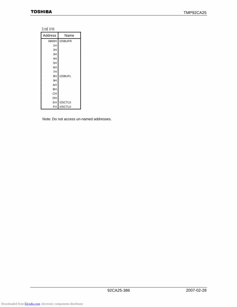
TMP92CA25
2007-02-28 92CA25-386
[19] I2S Address Name
0800H I2SBUFR 1H 2H 3H 4H 5H 6H 7H 8H I2SBUFL 9H AH BH CH DH EH I2SCTL0 FH I2SCTL0
Note: Do not access un-named addresses.
Downloaded from Elcodis.com electronic components distributor
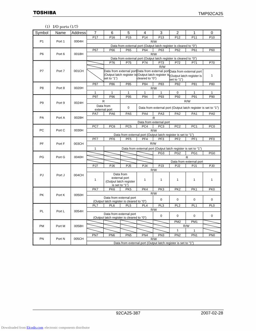
TMP92CA25
2007-02-28 92CA25-387
(1) I/O ports (1/7) Symbol Name Address 7 6 5 4 3 2 1 0
P17 P16 P15 P14 P13 P12 P11 P10 R/W P1 Port 1 0004H
Data from external port (Output latch register is cleared to “0”) P67 P66 P65 P64 P63 P62 P61 P60
R/W P6 Port 6 0018HData from external port (Output latch register is cleared to “0”)
P76 P75 P74 P73 P72 P71 P70 R/W
P7 Port 7 001CH Data from external port (Output latch register is set to “1”)
Data from external port (Output latch register is cleared to “0”)
Data from external port (Output latch register is set to “1”)
1
P87 P86 P85 P84 P83 P82 P81 P80 R/W P8 Port 8 0020H
1 1 1 1 1 0 1 1 P97 P96 P95 P94 P93 P92 P91 P90
R R/W P9 Port 9 0024HData from
external port 0 Data from external port (Output latch register is set to “1”)
PA7 PA6 PA5 PA4 PA3 PA2 PA1 PA0 R PA Port A 0028H
Data from external port PC7 PC6 PC5 PC4 PC3 PC2 PC1 PC0
R/W PC Port C 0030HData from external port (Output latch register is set to “1”)
PF7 PF6 PF5 PF4 PF3 PF2 PF1 PF0 R/W PF Port F 003CH
1 Data from external port (Output latch register is set to “1”) PG3 PG2 PG1 PG0 R PG Port G 0040H Data from external port
PJ7 PJ6 PJ5 PJ4 PJ3 PJ2 PJ1 PJ0 R/W
PJ Port J 004CH 1
Data from external port
(Output latch register is set to “1”)
1 1 1 1 1
PK7 PK6 PK5 PK4 PK3 PK2 PK1 PK0 R/W PK Port K 0050H
Data from external port (Output latch register is cleared to “0”) 0 0 0 0
PL7 PL6 PL5 PL4 PL3 PL2 PL1 PL0 R/W PL Port L 0054H
Data from external port (Output latch register is cleared to “0”) 0 0 0 0
PM2 PM1 R/W PM Port M 0058H 1 1
PN7 PN6 PN5 PN4 PN3 PN2 PN1 PN0 R/W PN Port N 005CH
Data from external port (Output latch register is set to “1”)
Downloaded from Elcodis.com electronic components distributor
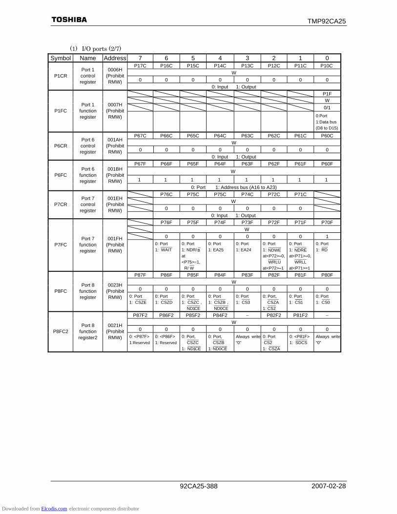
TMP92CA25
2007-02-28 92CA25-388
(1) I/O ports (2/7)
Symbol Name Address 7 6 5 4 3 2 1 0 P17C P16C P15C P14C P13C P12C P11C P10C
W 0 0 0 0 0 0 0 0
P1CR Port 1 control register
0006H (Prohibit RMW)
0: Input 1: Output P1F W 0/1 P1FC
Port 1 function register
0007H (Prohibit RMW)
0:Port 1:Data bus (D8 to D15)
P67C P66C P65C P64C P63C P62C P61C P60C W
0 0 0 0 0 0 0 0 P6CR
Port 6 control register
001AH (Prohibit RMW)
0: Input 1: Output P67F P66F P65F P64F P63F P62F P61F P60F
W
1 1 1 1 1 1 1 1 P6FC
Port 6 function register
001BH (Prohibit RMW)
0: Port 1: Address bus (A16 to A23) P76C P75C P75C P74C P72C P71C W 0 0 0 0 0 0
P7CR Port 7 control register
001EH (Prohibit RMW)
0: Input 1: Output P76F P75F P74F P73F P72F P71F P70F W 0 0 0 0 0 0 1
P7FC Port 7
function register
001FH (Prohibit RMW)
0: Port 1: WAIT
0: Port 1: NDR/B at <P75>=1,
R/ W
0: Port 1: EA25
0: Port 1: EA24
0: Port 1: NDWE at<P72>=0,
WRLU at<P72>=1
0: Port 1: NDRE at<P71>=0,
WRLL at<P71>=1
0: Port 1: RD
P87F P86F P85F P84F P83F P82F P81F P80F W
0 0 0 0 0 0 0 0 P8FC Port 8
function register
0023H (Prohibit RMW) 0: Port
1: CSZE 0: Port 1: CSZD
0: Port 1: CSZC ,
CE1ND
0: Port 1: CSZB , CE0ND
0: Port 1: 3CS
0: Port, CSZA 1: 2CS
0: Port 1: 1CS
0: Port 1: 0CS
P87F2 P86F2 P85F2 P84F2 − P82F2 P81F2 − W
0 0 0 0 0 0 0 0 P8FC2 Port 8
function register2
0021H (Prohibit RMW) 0: <P87F>
1:Reserved 0: <P86F>1: Reserved
0: Port, CSZC
1: CE1ND
0: Port, CSZB 1: CE0ND
Always write “0”
0: Port 2CS
1: CSZA
0: <P81F> 1: SDCS
Always write“0”
Downloaded from Elcodis.com electronic components distributor

TMP92CA25
2007-02-28 92CA25-389
(1) I/O ports (3/7)
Symbol Name Address 7 6 5 4 3 2 1 0 P95C P94C P93C P92C P91C P90C W 0 0 0 0 0 0
P9CR Port 9 control register
0026H(Prohibit RMW)
0: Port 1: CLK32KO
0: Port 1: Port,
SCL
0:Port 1: Port, SDA
0:Port, SCLK0,
0CTS I2SWS
1:Port, SCLK0
0: Port, RXD0 I2SDO
1: Port
0:Port, I2SCKO
1: Port, TXD0
P97F P96F P95F P94F P93F P92F P91F P90F W
0 0 0 0 0 0 0 0
P9FC Port 9
function register
0027H(Prohibit RMW)
0: Port 1: INT5
0: Port 1: INT4
0:Port, CLK32KO1: Reserved
0: Port 1: SCL
0: Port 1: SDA
0: Port, SCLK0,
0CTS 1: I2SWS,
SCLK0
0: Port, RXD0
1: I2SDO
0: Port 1: I2SCKO,
TXD0
P94F2 P93F2 P90FC2 W W 0 0 0 P9FC2
Port 9 function register2
0025H(Prohibit RMW) 0: CMOS
1: Open drain
0: CMOS 1: Open drain
0: CMOS 1: Open
drain PA7F PA6F PA5F PA4F PA3F PA2F PA1F PA0F
W 0 0 0 0 0 0 0 0
PAFC Port A
function register
002BH(Prohibit RMW)
0: Key-in disable 1: Key-in enable PC7C PC6C PC5C PC4C PC3C PC2C PC1C PC0C
W 0 0 0 0 0 0 0 0 PCCR
Port C control register
0032H(Prohibit RMW)
0: Input 1: Output
PC7F PC6F PC5F PC4F PC3F PC2F PC1F PC0F W
0 0 0 0 0 0 0 0
PCFC Port C
function register
0033H(Prohibit RMW)
0: Port 1: CSZF , EA25 at <PC7> = 0
0: Port 1:KO8 (Open -Drain)EA24 at <PC6> = 0
0: Port 1:Reserved
0: Port 1:Reserved
0: Port 1: INT3
0: Port 1: INT2, TB0OUT0
0: Port 1: INT1, TA3OUT
0: Port 1: INT0, TA1OUT
Downloaded from Elcodis.com electronic components distributor

TMP92CA25
2007-02-28 92CA25-390
(1) I/O ports (4/7)
Symbol Name Address 7 6 5 4 3 2 1 0 PF6C PF5C PF4C PF3C PF2C PF1C PF0C W 0 0 0 0 0 0 0
PFCR Port F control register
003EH(Prohibit RMW)
0: Port 1: Port
0: Port 1: Port
0: Port 1: Port
0: Port 1: Port
0: Port, SCLK0,
0CTS ,
(From PF2 at <PF2> = 0)
(from P92 at
<PF2> = 1) 1: Port,
SCLK0
0: Port, RXD0
1: Port
0: Port 1: Port,
TXD0
PF7F PF6F PF5F PF4F PF3F PF2F PF1F PF0F W
0 0 0 0 0 0 0 0
PFFC Port F
function register
003FH(Prohibit RMW)
0: Port 1: SDCLK
0: Port 1: Reserved
0: Port 1:Reserved
0: Port 1:Reserved
0: Port 1:Reserved
0: Port,
SCLK0, 0CTS
(from PF2 at <PF2>=0)
(from P92 at
<PF2> =1) 1:SCLK0
0: Port RXD0 (from PF1 pin) 1: RXD0 (from P91 pin)
0: Port 1: TXD0
− − PF0F2 W W W 0 0 0
PFFC2 Port F
function register2
003DH(Prohibit RMW) Always
write “0” Always
write “0” Output buffer
0: CMOS 1: Open-drain
PJ6C PJ5C W 0 0
PJCR Port J control register
004EH(Prohibit RMW)
0:Input 1: Output
PJ7F PJ6F PJ5F PJ4F PJ3F PJ2F PJ1F PJ0F
W
0 0 0 0 0 0 0 0 PJFC
Port J function register
004FH(Prohibit RMW)
0: Port 1: SDCKE at <PJ7>=1
0: Port 1: NDCLE at
<PJ6>=0
0: Port 1: NDALE at
<PJ5>=0
0: Port 1: SDLUDQM at <PJ4>=1
0: Port 1: SDLLDQM at <PJ3>=1
0: Port 1: SDWE , SDWR
0: Port 1: SDCAS , SRLUB
0: Port 1: SDRAS , SRLLB
PK7C PK7C PK7C PK7C
W
0 0 0 0 PKCR
Port K Control Register
0052H(Prohibit RMW)
0:Input 1: Output
PK7F PK6F PK5F PK4F PK3F PK2F PK1F PK0F
W
0 0 0 0 0 0 0 0 PKFC Port K
function register
0053H(Prohibit RMW)
0: Port 1: SPCLK
0: Port 1: SPCS
0: Port 1: SPDO
0: Port 1: SPDI
0: Port 1: LBCD
0: Port 1: LFR
0: Port 1: LLP
0: Port 1: LCP0
Downloaded from Elcodis.com electronic components distributor

TMP92CA25
2007-02-28 92CA25-391
(1) I/O ports (5/7) Symbol Name Address 7 6 5 4 3 2 1 0
PL7C PL6C PL5C PL4C
W
0 0 0 0 PLCR
Port L control register
0056H(Prohibit RMW)
0: Input 1: Output
PL7F PL6F PL5F PL4F PL3F PL2F PL1F PL0F
W
0 0 0 0 0 0 0 0 PLFC Port L
function register
0057H(Prohibit RMW) 0: Port
1: LD7, BUSAK
0: Port 1: LD6, BUSRQ
0: Port 1: LD5
0: Port 1: LD4 0: Port 1: Data bus for LCDC (LD3 to LD0)
PM2F PM1F
W
0 0 PMFC Port M function register
005BH(Prohibit RMW) 0: Port
1: ALARM MLDALM
0: Port 1: MLDALM
output
PN7C PN6C PN5C PN4C PN3C PN2C PN1C PN0C W
0 0 0 0 0 0 0 0 PNCR
Port N Control Register
005EH(Prohibit RMW)
0:Input 1: Output
PN7F PN6F PN5F PN4F PN3F PN2F PN1F PN0F
W
0 0 0 0 0 0 0 0 PNFC
Port N Function Register
005FH(Prohibit RMW)
0: CMOS output 1: Open drain output
Downloaded from Elcodis.com electronic components distributor

TMP92CA25
2007-02-28 92CA25-392
(1) I/O ports (6/7)
Symbol Name Address 7 6 5 4 3 2 1 0 P17D P16D P15D P14D P13D P12D P11D P10D
R/W
1 1 1 1 1 1 1 1 P1DR
Port 1 drive
register 0081H
Input/Output buffer drive register for standby mode P47D P46D P45D P44D P43D P42D P41D P40D
R/W
1 1 1 1 1 1 1 1 P4DR
Port 4 drive
register 0084H
Input/Output buffer drive register for standby mode P57D P56D P55D P54D P53D P52D P51D P50D
R/W
1 1 1 1 1 1 1 1 P5DR
Port 5 drive
register 0085H
Input/Output buffer drive register for standby mode P67D P66D P65D P64D P63D P62D P61D P60D
R/W
1 1 1 1 1 1 1 1 P6DR
Port 6 drive
register 0086H
Input/Output buffer drive register for standby mode P76D P75D P74D P73D P72D P71D P70D R/W
1 1 1 1 1 1 1 P7DR
Port 7 drive
register 0087H
Input/Output buffer drive register for standby mode P87D P86D P85D P84D P83D P82D P81D P80D
R/W
1 1 1 1 1 1 1 1 P8DR
Port 8 drive
register 0088H
Input/Output buffer drive register for standby mode P97D P96D P95D P94D P93D P92D P91D P90D
R/W
1 1 1 1 1 1 1 1 P9DR
Port 9 drive
register 0089H
Input/Output buffer drive register for standby mode PA7D PA6D PA5D PA4D PA3D PA2D PA1D PA0D
R/W
1 1 1 1 1 1 1 1 PADR
Port A drive
register 008AH
Input/Output buffer drive register for standby mode PC7D PC6D PC5D PC4D PC3D PC2D PC1D PC0D
R/W
1 1 1 1 1 1 1 1 PCDR
Port C drive
register 008CH
Input/Output buffer drive register for standby mode PF7D PF6D PF5D PF4D PF3D PF2D PF1D PF0D
R/W
1 1 1 1 1 1 1 1 PFDR
Port F drive
register 008FH
Input/Output buffer drive register for standby mode PG3D PG2D R/W
1 1 PGDR Port G drive
register 0090H
Input/Output buffer
drive register for standby mode
Downloaded from Elcodis.com electronic components distributor

TMP92CA25
2007-02-28 92CA25-393
(1) I/O ports (7/7)
Symbol Name Address 7 6 5 4 3 2 1 0 PJ7D PJ6D PJ5D PJ4D PJ3D PJ2D PJ1D PJ0D
R/W 1 1 1 1 1 1 1 1 PJDR
Port J drive
register 0093H
Input/Output buffer drive register for standby mode
PK7D PK6D PK5D PK4D PK3D PK2D PK1D PK0D
R/W
1 1 1 1 1 1 1 1 PKDR
Port K drive
register 0094H
Input/Output buffer drive register for standby mode PL7D PL6D PL5D PL4D PL3D PL2D PL1D PL0D
R/W 1 1 1 1 1 1 1 1
PLDR Port L drive
register 0095H
Input/Output buffer drive register for standby mode PM2D PM1D R/W 1 1 PMDR
Port M drive
register 0096H
Input/Output buffer drive register
for standby mode
PN7D PN6D PN5D PN4D PN3D PN2D PN1D PN0D R/W
1 1 1 1 1 1 1 1 PNDR
Port N drive
register 0097H
Input/Output buffer drive register for standby mode
Downloaded from Elcodis.com electronic components distributor

TMP92CA25
2007-02-28 92CA25-394
(2) Interrupt control (1/4)
Symbol Name Address 7 6 5 4 3 2 1 0 INT2 INT1
I2C I2M2 I2M1 I2M0 I1C I1M2 I1M1 I1M0 R R/W R R/W
INTE12 INT1 & INT2 enable 00D0H
0 0 0 0 0 0 0 0 INT4 INT3
I4C I4M2 I4M1 I4M0 I3C I3M2 I3M1 I3M0 R R/W R R/W
INTE34 INT3 & INT4 enable 00D1H
0 0 0 0 0 0 0 0 INTTA1 (TMRA1) INTTA0 (TMRA0)
ITA1C ITA1M2 ITA1M1 ITA1M0 ITA0C ITA0M2 ITA0M1 ITA0M0R R/W R R/W
INTETA01 INTTA0 & INTTA1 enable
00D4H
0 0 0 0 0 0 0 0 INTTA3 (TMRA3) INTTA2 (TMRA2)
ITA3C ITA3M2 ITA3M1 ITA3M0 ITA2C ITA2M2 ITA2M1 ITA2M0R R/W R R/W
INTETA23 INTTA2 & INTTA3 enable
00D5H
0 0 0 0 0 0 0 0 INTTB1 (TMRB1) INTTB0 (TMRB0)
ITB1C ITB1M2 ITB1M1 ITB1M0 ITB0C ITB0M2 ITB0M1 ITB0M0R R/W R R/W
INTETB01 INTTB0 & INTTB1 enable
00D8H
0 0 0 0 0 0 0 0 − INTTBO0 (TMRB0)
− − − − ITBO0C ITBO0M2 ITBO0M1 ITBO0M0− − R R/W
INTETBO0 INTTBO0 (Overflow)
enable 00DAH
Always write “0” 0 0 0 0 INTTX0 INTRX0
ITX0C ITX0M2 ITX0M1 ITX0M0 IRX0C IRX0M2 IRX0M1 IRX0M0R R/W R R/W
INTES0 INTRX0 & INTTX0 enable
00DBH
0 0 0 0 0 0 0 0 INTSPI −
ISPIC ISPIM2 ISPIM1 ISPIM0 − − − − R R/W − −
INTESPI INTSPI enable 00E0H
0 0 0 0 Always write “0” − INTSBI
− − − − ISBIC ISBIM2 ISBIM1 ISBIM0− − R R/W
INTESBI INTSBI enable 00E1H
Always write “0” 0 0 0 0 INTALM1 INTALM0
IA1C IA1M2 IA1M1 IA1M0 IA0C IA0M2 IA0M1 IA0M0 R R/W R R/W
INTEALM01 INTALM0 & INTALM1
enable 00E5H
0 0 0 0 0 0 0 0 INTALM3 INTALM2
IA3C IA3M2 IA3M1 IA3M0 IA2C IA2M2 IA2M1 IA2M0 R R/W R R/W
INTEALM23 INTALM2 & INTALM3
enable 00E6H
0 0 0 0 0 0 0 0
Downloaded from Elcodis.com electronic components distributor
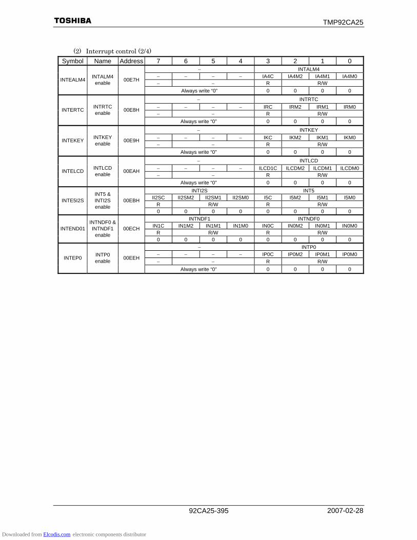
TMP92CA25
2007-02-28 92CA25-395
(2) Interrupt control (2/4)
Symbol Name Address 7 6 5 4 3 2 1 0 − INTALM4
− − − − IA4C IA4M2 IA4M1 IA4M0 − − R R/W
INTEALM4 INTALM4 enable 00E7H
Always write “0” 0 0 0 0
− INTRTC − − − − IRC IRM2 IRM1 IRM0 − − R R/W
INTERTC INTRTC enable 00E8H
Always write “0” 0 0 0 0
− INTKEY − − − − IKC IKM2 IKM1 IKM0 − − R R/W
INTEKEY INTKEY enable 00E9H
Always write “0” 0 0 0 0
− INTLCD − − − − ILCD1C ILCDM2 ILCDM1 ILCDM0− − R R/W
INTELCD INTLCD enable 00EAH
Always write “0” 0 0 0 0 INTI2S INT5
II2SC II2SM2 II2SM1 II2SM0 I5C I5M2 I5M1 I5M0 R R/W R R/W
INTE5I2S INT5 & INTI2S enable
00EBH
0 0 0 0 0 0 0 0 INTNDF1 INTNDF0
IN1C IN1M2 IN1M1 IN1M0 IN0C IN0M2 IN0M1 IN0M0 R R/W R R/W
INTEND01 INTNDF0 & INTNDF1
enable 00ECH
0 0 0 0 0 0 0 0 − INTP0
− − − − IP0C IP0M2 IP0M1 IP0M0 − − R R/W
INTEP0 INTP0 enable 00EEH
Always write “0” 0 0 0 0
Downloaded from Elcodis.com electronic components distributor

TMP92CA25
2007-02-28 92CA25-396
(2) Interrupt control (3/4)
Symbol Name Address 7 6 5 4 3 2 1 0 INTAD INT0
IADC IADM2 IADM1 IADM0 I0C I0M2 I0M1 I0M0 R R/W R R/W
INTE0AD INT0 & INTAD enable
00F0H
0 0 0 0 0 0 0 0 INTTC1 (DMA1) INTTC0 (DMA0)
ITC1C ITC1M2 ITC1M1 ITC1M0 ITC0C ITC0M2 ITC0M1 ITC0M0R R/W R R/W
INTETC01 INTTC0 & INTTC1 enable
00F1H
0 0 0 0 0 0 0 0 INTTC3 (DMA3) INTTC2 (DMA2)
ITC3C ITC3M2 ITC3M1 ITC3M0 ITC2C ITC2M2 ITC2M1 ITC2M0R R/W R R/W
INTETC23 INTTC2 & INTTC3 enable
00F2H
0 0 0 0 0 0 0 0 INTTC5 (DMA5) INTTC4 (DMA4)
ITC5C ITC5M2 ITC5M1 ITC5M0 ITC4C ITC4M2 ITC4M1 ITC4M0R R/W R R/W
INTETC45 INTTC4 & INTTC5 enable
00F3H
0 0 0 0 0 0 0 0 INTTC7 (DMA7) INTTC6 (DMA6)
ITC7C ITC7M2 ITC7M1 ITC7M0 ITC6C ITC6M2 ITC6M1 ITC6M0R R/W R R/W
INTETC67 INTTC6 & INTTC7 enable
00F4H
0 0 0 0 0 0 0 0 − − IR0LE W W 0 1 1
SIMC
SIO interrupt
mode control
00F5H (Prohibit RMW)
Always write “0”.
Always write “1”.
0: INTRX0 edge mode
1: INTRX0 level mode
I5EDGE I4EDGE I3EDGE I2EDGE I1EDGE I0EDGE I0LE − W R/W
0 0 0 0 0 0 0 0
IIMC Interrupt
input mode control
00F6H (Prohibit RMW)
INT5 edge 0: Rising 1: Falling
INT4 edge 0: Rising1: Falling
INT3 edge 0: Rising1: Falling
INT2 edge 0: Rising1: Falling
INT1 edge 0: Rising1: Falling
INT0 edge 0: Rising 1: Falling
0: INT0 edge mode
1:INT0 level mode
Always write “0”.
− INTWD − − − − ITCWD − − − − − R
INTWDT INTWD enable 00F7H
Always write “0” 0 − − − CLRV7 CLRV6 CLRV5 CLRV4 CLRV3 CLRV2 CLRV1 CLRV0
W 0 0 0 0 0 0 0 0
INTCLR Interrupt clear control
00F8H (Prohibit RMW)
Interrupt vector
Downloaded from Elcodis.com electronic components distributor

TMP92CA25
2007-02-28 92CA25-397
(2) Interrupt control (4/4)
Symbol Name Address 7 6 5 4 3 2 1 0 DMA0V5 DMA0V4 DMA0V3 DMA0V2 DMA0V1 DMA0V0 R/W 0 0 0 0 0 0
DMA0V DMA0 start vector 0100H
DMA0 start vector DMA1V5 DMA1V4 DMA1V3 DMA1V2 DMA1V1 DMA1V0 R/W 0 0 0 0 0 0
DMA1V DMA1 start vector 0101H
DMA1 start vector DMA2V5 DMA2V4 DMA2V3 DMA2V2 DMA2V1 DMA2V0 R/W 0 0 0 0 0 0
DMA2V DMA2 start vector 0102H
DMA2 start vector DMA3V5 DMA3V4 DMA3V3 DMA3V2 DMA3V1 DMA3V0 R/W 0 0 0 0 0 0
DMA3V DMA3 start vector 0103H
DMA3 start vector DMA4V5 DMA4V4 DMA4V3 DMA4V2 DMA4V1 DMA4V0 R/W 0 0 0 0 0 0
DMA4V DMA4 start vector 0104H
DMA4 start vector DMA5V5 DMA5V4 DMA5V3 DMA5V2 DMA5V1 DMA5V0 R/W 0 0 0 0 0 0
DMA5V DMA5 start vector 0105H
DMA5 start vector DMA6V5 DMA6V4 DMA6V3 DMA6V2 DMA6V1 DMA6V0 R/W 0 0 0 0 0 0
DMA6V DMA6 start vector 0106H
DMA6 start vector DMA7V5 DMA7V4 DMA7V3 DMA7V2 DMA7V1 DMA7V0 R/W 0 0 0 0 0 0
DMA7V DMA7 start vector 0107H
DMA7 start vector DBST7 DBST6 DBST5 DBST4 DBST3 DBST2 DBST1 DBST0
R/W 0 0 0 0 0 0 0 0
DMAB DMA burst 0108H
1: DMA request on burst mode DREQ7 DREQ6 DREQ5 DREQ4 DREQ3 DREQ2 DREQ1 DREQ0
R/W 0 0 0 0 0 0 0 0
DMAR DMA request
0109H (Prohibit RMW)
1: DMA request in software
Downloaded from Elcodis.com electronic components distributor
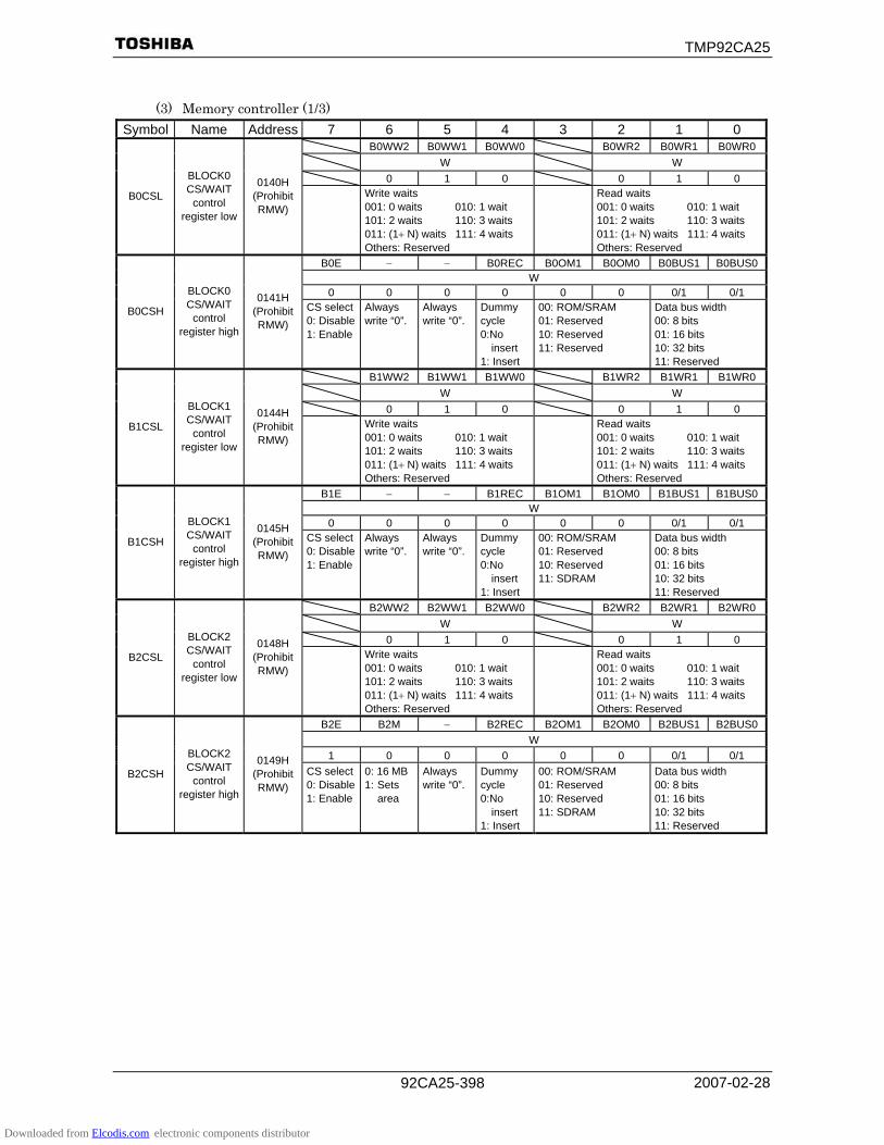
TMP92CA25
2007-02-28 92CA25-398
(3) Memory controller (1/3)
Symbol Name Address 7 6 5 4 3 2 1 0 B0WW2 B0WW1 B0WW0 B0WR2 B0WR1 B0WR0 W W 0 1 0 0 1 0
B0CSL
BLOCK0 CS/WAIT
control register low
0140H (Prohibit RMW)
Write waits 001: 0 waits 010: 1 wait 101: 2 waits 110: 3 waits 011: (1+ N) waits 111: 4 waits Others: Reserved
Read waits 001: 0 waits 010: 1 wait 101: 2 waits 110: 3 waits 011: (1+ N) waits 111: 4 waits Others: Reserved
B0E − − B0REC B0OM1 B0OM0 B0BUS1 B0BUS0W
0 0 0 0 0 0 0/1 0/1
B0CSH
BLOCK0 CS/WAIT
control register high
0141H (Prohibit RMW)
CS select 0: Disable 1: Enable
Always write “0”.
Always write “0”.
Dummy cycle 0:No
insert 1: Insert
00: ROM/SRAM 01: Reserved 10: Reserved 11: Reserved
Data bus width 00: 8 bits 01: 16 bits 10: 32 bits 11: Reserved
B1WW2 B1WW1 B1WW0 B1WR2 B1WR1 B1WR0 W W 0 1 0 0 1 0
B1CSL
BLOCK1 CS/WAIT
control register low
0144H (Prohibit RMW)
Write waits 001: 0 waits 010: 1 wait 101: 2 waits 110: 3 waits 011: (1+ N) waits 111: 4 waits Others: Reserved
Read waits 001: 0 waits 010: 1 wait 101: 2 waits 110: 3 waits 011: (1+ N) waits 111: 4 waits Others: Reserved
B1E − − B1REC B1OM1 B1OM0 B1BUS1 B1BUS0W
0 0 0 0 0 0 0/1 0/1
B1CSH
BLOCK1 CS/WAIT
control register high
0145H (Prohibit RMW)
CS select 0: Disable 1: Enable
Always write “0”.
Always write “0”.
Dummy cycle 0:No
insert 1: Insert
00: ROM/SRAM 01: Reserved 10: Reserved 11: SDRAM
Data bus width 00: 8 bits 01: 16 bits 10: 32 bits 11: Reserved
B2WW2 B2WW1 B2WW0 B2WR2 B2WR1 B2WR0 W W 0 1 0 0 1 0
B2CSL
BLOCK2 CS/WAIT
control register low
0148H (Prohibit RMW)
Write waits 001: 0 waits 010: 1 wait 101: 2 waits 110: 3 waits 011: (1+ N) waits 111: 4 waits Others: Reserved
Read waits 001: 0 waits 010: 1 wait 101: 2 waits 110: 3 waits 011: (1+ N) waits 111: 4 waits Others: Reserved
B2E B2M − B2REC B2OM1 B2OM0 B2BUS1 B2BUS0W
1 0 0 0 0 0 0/1 0/1
B2CSH
BLOCK2 CS/WAIT
control register high
0149H (Prohibit RMW)
CS select 0: Disable 1: Enable
0: 16 MB1: Sets area
Always write “0”.
Dummy cycle 0:No
insert 1: Insert
00: ROM/SRAM 01: Reserved 10: Reserved 11: SDRAM
Data bus width 00: 8 bits 01: 16 bits 10: 32 bits 11: Reserved
Downloaded from Elcodis.com electronic components distributor
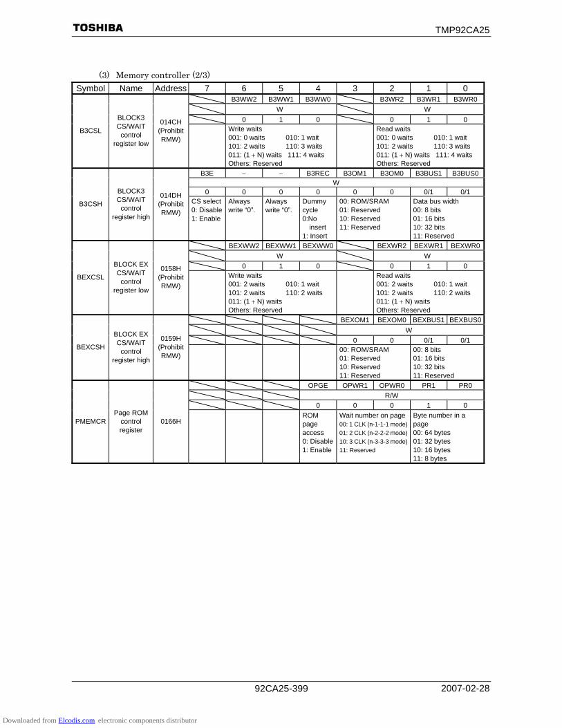
TMP92CA25
2007-02-28 92CA25-399
(3) Memory controller (2/3) Symbol Name Address 7 6 5 4 3 2 1 0
B3WW2 B3WW1 B3WW0 B3WR2 B3WR1 B3WR0 W W 0 1 0 0 1 0
B3CSL
BLOCK3 CS/WAIT
control register low
014CH(Prohibit RMW)
Write waits 001: 0 waits 010: 1 wait 101: 2 waits 110: 3 waits 011: (1 + N) waits 111: 4 waits Others: Reserved
Read waits 001: 0 waits 010: 1 wait 101: 2 waits 110: 3 waits 011: (1 + N) waits 111: 4 waits Others: Reserved
B3E − − B3REC B3OM1 B3OM0 B3BUS1 B3BUS0W
0 0 0 0 0 0 0/1 0/1
B3CSH
BLOCK3 CS/WAIT
control register high
014DH(Prohibit RMW)
CS select 0: Disable 1: Enable
Always write “0”.
Always write “0”.
Dummy cycle 0:No
insert 1: Insert
00: ROM/SRAM 01: Reserved 10: Reserved 11: Reserved
Data bus width 00: 8 bits 01: 16 bits 10: 32 bits 11: Reserved
BEXWW2 BEXWW1 BEXWW0 BEXWR2 BEXWR1 BEXWR0 W W 0 1 0 0 1 0
BEXCSL
BLOCK EX CS/WAIT
control register low
0158H(Prohibit RMW)
Write waits 001: 2 waits 010: 1 wait 101: 2 waits 110: 2 waits 011: (1 + N) waits Others: Reserved
Read waits 001: 2 waits 010: 1 wait 101: 2 waits 110: 2 waits 011: (1 + N) waits Others: Reserved
BEXOM1 BEXOM0 BEXBUS1 BEXBUS0 W 0 0 0/1 0/1
BEXCSH
BLOCK EX CS/WAIT
control register high
0159H(Prohibit RMW)
00: ROM/SRAM 01: Reserved 10: Reserved 11: Reserved
00: 8 bits 01: 16 bits 10: 32 bits 11: Reserved
OPGE OPWR1 OPWR0 PR1 PR0 R/W 0 0 0 1 0
PMEMCR Page ROM
control register
0166H ROM
page access 0: Disable1: Enable
Wait number on page 00: 1 CLK (n-1-1-1 mode) 01: 2 CLK (n-2-2-2 mode) 10: 3 CLK (n-3-3-3 mode) 11: Reserved
Byte number in a page 00: 64 bytes 01: 32 bytes 10: 16 bytes 11: 8 bytes
Downloaded from Elcodis.com electronic components distributor

TMP92CA25
2007-02-28 92CA25-400
(3) Memory controller (3/3)
Symbol Name Address 7 6 5 4 3 2 1 0 M0V20 M0V19 M0V18 M0V17 M0V16 M0V15 M0V14-9 M0V8
R/W 1 1 1 1 1 1 1 1
MAMR0
Memory address
mask register 0
0142H
0: Compare enable 1: Compare disable M0S23 M0S22 M0S21 M0S20 M0S19 M0S18 M0S17 M0S16
R/W 1 1 1 1 1 1 1 1
MSAR0
Memory start
address register 0
0143H
Set start address A23 to A16 M1V21 M1V20 M1V19 M1V18 M1V17 M1V16 MV15-9 M1V8
R/W 1 1 1 1 1 1 1 1
MAMR1
Memory address
mask register 1
0146H
0: Compare enable 1: Compare disable M1S23 M1S22 M1S21 M1S20 M1S19 M1S18 M1S17 M1S16
R/W 1 1 1 1 1 1 1 1
MSAR1
Memory start
address register 1
0147H
Set start address A23 to A16 M2V22 M2V21 M2V20 M2V19 M2V18 M2V17 M2V16 M2V15
R/W 1 1 1 1 1 1 1 1
MAMR2
Memory address
mask register 2
014AH
0: Compare enable 1: Compare disable M2S23 M2S22 M2S21 M2S20 M2S19 M2S18 M2S17 M2S16
R/W 1 1 1 1 1 1 1 1
MSAR2
Memory start
address register 2
014BH
Set start address A23 to A16 M3V22 M3V21 M3V20 M3V19 M3V18 M3V17 M3V16 M3V15
R/W 1 1 1 1 1 1 1 1
MAMR3
Memory address
mask register 3
014EH
0:Compare enable 1:Compare disable M3S23 M3S22 M3S21 M3S20 M3S19 M3S18 M3S17 M3S16
R/W 1 1 1 1 1 1 1 1
MSAR3
Memory start
address register 3
014FH
Set start address A23 to A16 CSDIS RDTMG1 RDTMG0 R/W 0 0 0
MEMCR0 Memory control
register 0 0168H
0: Disable 1: Enable
00: RD “H” pulse width = 0.5T (Default)01: RD “H” pulse width = 0.75T 10: RD “H” pulse width =1.0T11: Reserved
Downloaded from Elcodis.com electronic components distributor
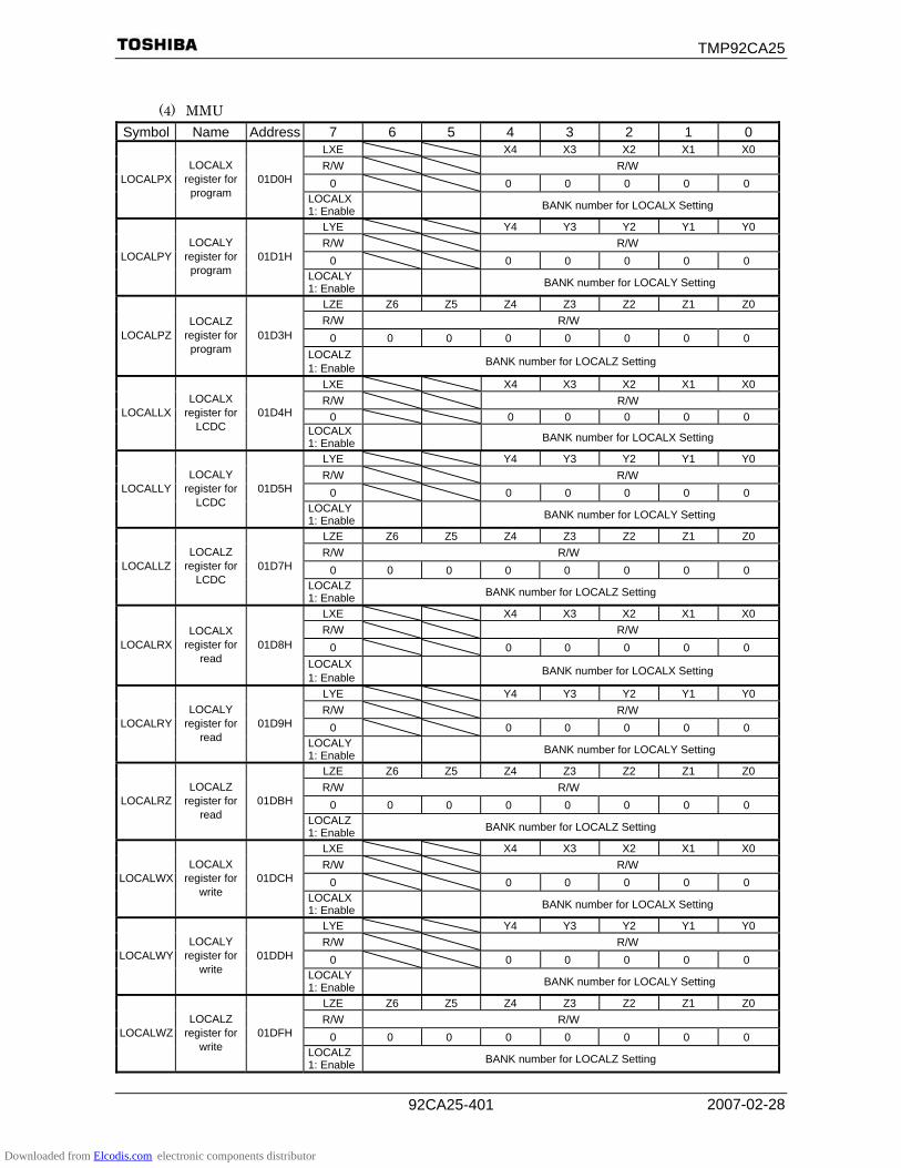
TMP92CA25
2007-02-28 92CA25-401
(4) MMU
Symbol Name Address 7 6 5 4 3 2 1 0 LXE X4 X3 X2 X1 X0 R/W R/W
0 0 0 0 0 0 LOCALPX LOCALX
register for program
01D0H
LOCALX 1: Enable
BANK number for LOCALX Setting
LYE Y4 Y3 Y2 Y1 Y0 R/W R/W
0 0 0 0 0 0 LOCALPY LOCALY
register for program
01D1H
LOCALY 1: Enable
BANK number for LOCALY Setting
LZE Z6 Z5 Z4 Z3 Z2 Z1 Z0 R/W R/W
0 0 0 0 0 0 0 0 LOCALPZ LOCALZ
register for program
01D3H
LOCALZ 1: Enable BANK number for LOCALZ Setting
LXE X4 X3 X2 X1 X0 R/W R/W
0 0 0 0 0 0 LOCALLX LOCALX
register for LCDC
01D4HLOCALX 1: Enable
BANK number for LOCALX Setting
LYE Y4 Y3 Y2 Y1 Y0 R/W R/W
0 0 0 0 0 0 LOCALLY LOCALY
register for LCDC
01D5H
LOCALY 1: Enable
BANK number for LOCALY Setting
LZE Z6 Z5 Z4 Z3 Z2 Z1 Z0 R/W R/W
0 0 0 0 0 0 0 0 LOCALLZ LOCALZ
register for LCDC
01D7H
LOCALZ 1: Enable BANK number for LOCALZ Setting
LXE X4 X3 X2 X1 X0 R/W R/W
0 0 0 0 0 0 LOCALRX LOCALX
register for read
01D8H
LOCALX 1: Enable
BANK number for LOCALX Setting
LYE Y4 Y3 Y2 Y1 Y0 R/W R/W
0 0 0 0 0 0 LOCALRY LOCALY
register for read
01D9H
LOCALY 1: Enable
BANK number for LOCALY Setting
LZE Z6 Z5 Z4 Z3 Z2 Z1 Z0 R/W R/W
0 0 0 0 0 0 0 0 LOCALRZ LOCALZ
register for read
01DBH
LOCALZ 1: Enable BANK number for LOCALZ Setting
LXE X4 X3 X2 X1 X0 R/W R/W
0 0 0 0 0 0 LOCALWX LOCALX
register for write
01DCH
LOCALX 1: Enable
BANK number for LOCALX Setting
LYE Y4 Y3 Y2 Y1 Y0 R/W R/W
0 0 0 0 0 0 LOCALWY LOCALY
register for write
01DDH
LOCALY 1: Enable
BANK number for LOCALY Setting
LZE Z6 Z5 Z4 Z3 Z2 Z1 Z0 R/W R/W
0 0 0 0 0 0 0 0 LOCALWZ LOCALZ
register for write
01DFH
LOCALZ 1: Enable BANK number for LOCALZ Setting
Downloaded from Elcodis.com electronic components distributor

TMP92CA25
2007-02-28 92CA25-402
(5) Clock gear, PLL
Symbol Name Address 7 6 5 4 3 2 1 0 XEN XTEN WUEF
R/W R/W 1 1 0
SYSCR0 System
clock control register 0
10E0H H-OSC (fc) 0: Stop
1: Oscillation
L-OSC (fs) 0: Stop
1: Oscillation
Warm-up timer
SYSCK GEAR2 GEAR1 GEAR0 R/W 0 1 0 0
SYSCR1 System
clock control register 1
10E1H Select
system clock 0: fc 1: fs
Select gear value of high frequency (fc) 000: fc 101: (Reserved) 001: fc/2 110: (Reserved) 010: fc/4 111: (Reserved) 011: fc/8 100: fc/16
− WUPTM1 WUPTM0 HALTM1 HALTM0 R/W R/W
0 1 0 1 1
SYSCR2 System
clock control register 2
10E2H Always write “0”
Warm-up timer 00: Reserved 01: 28/Inputted frequency10: 214/Inputted frequency11: 216/Inputted frequency
HALT mode 00: Reserved 01: STOP mode 10: IDLE1 mode 11: IDLE2 mode
PROTECT EXTIN DRVOSCH DRVOSCLR R/W 0 0 1 1
EMCCR0 EMC
control register 0
10E3H Protect flag 0: OFF 1: ON
1: External clock
High frequency oscillator driver ability 1: NORMAL0: WEAK
Low frequency oscillator driver ability 1: NORMAL0: WEAK
EMCCR1 EMC
control register 1
10E4H
EMCCR2 EMC
control register 2
10E5H
Switching the protect ON/OFF by write to following 1st KEY, 2nd KEY 1st KEY: EMCCR1=5AH, EMCCR2=A5H in succession write 2nd KEY: EMCCR1=A5H, EMCCR2=5AH in succession write
FCSEL LUPFG R/W R 0 0
PLLCR0 PLL
control register 0
10E8H Select fc clock 0: fOSCH1: fPLL
Lock up timer status flag
PLLON R/W
0 PLLCR1
PLL control
register 1 10E9H Control
on/off 0: OFF 1: ON
Downloaded from Elcodis.com electronic components distributor
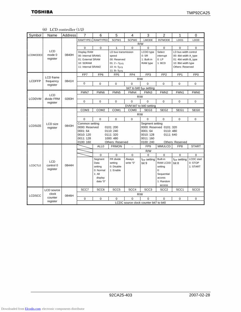
TMP92CA25
2007-02-28 92CA25-403
(6) LCD controller (1/2)
Symbol Name Address 7 6 5 4 3 2 1 0 RAMTYPE1 RAMTYPE0 SCPW1 SCPW0 LMODE INTMODE LDO1 LDO0
R/W 0 0 1 0 0 0 0 0
LCDMODE0 LCD
mode 0 register
0840H Display RAM 00: Internal SRAM1 01: External SRAM 10: SDRAM 11: Internal SRAM2
LD bus transmission speed 00: Reserved 01: 2 × fSYS 10: 4× fSYS 11: 8× fSYS
LCDD type0: SR 1: Built-in RAM type
Select interrupt 0: LP 1: BCD
LD bus width control 00: 4bit width A_type 01: 4bit width B_type 10: 8bit width type Others: Reserved
FP7 FP6 FP5 FP4 FP3 FP2 FP1 FP0 R/W
0 0 0 0 0 0 0 0 LCDFFP
LCD frame frequency register
0841H
bit7 to bit0 fFP setting FMN7 FMN6 FMN5 FMN4 FMN3 FMN2 FMN1 FMN0
R/W 0 0 0 0 0 0 0 0
LCDDVM LCD
divide FRM register
0283H
DVM bit7 to bit0 setting COM3 COM2 COM1 COM0 SEG3 SEG2 SEG1 SEG0
R/W 0 0 0 0 0 0 0 0
LCDSIZE LCD size register 0843H
Common setting 0000: Reserved 0101: 200 0001: 64 0110: 240 0010: 120 0111: 320 0011: 128 1000: 480 0100: 160 Others: Reserved
Segment setting 0000: Reserved 0101: 320 0001: 64 0110: 480 0010: 128 0111: 640 0011: 160 0100: 240 Others: Reserved
ALL0 FRMON − FP9 MMULCD FP8 START R/W 0 0 0 0 0 0 0
LCDCTL0 LCD
control 0 register
0844H
Segment Data setting 0: Normal 1: All
display data “0”
FR divide setting 0: Disable 1: Enable
Always write “0”
fFP setting bit 9
Built-in RAM LCDD setting 0: Sequential access 1: Random
access
fFP setting bit 8
LCDC start 0: STOP 1: START
SCC7 SCC6 SCC5 SCC4 SCC3 SCC2 SCC1 SCC0 R/W
0 0 0 0 0 0 0 0 LCDSCC
LCD source clock
counter register
0846H
LCDC source clock counter bit7 to bit0
Downloaded from Elcodis.com electronic components distributor
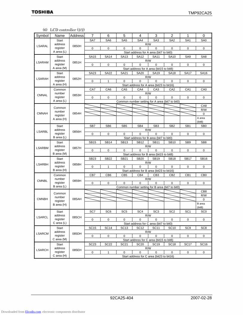
TMP92CA25
2007-02-28 92CA25-404
(6) LCD controller (2/2)
Symbol Name Address 7 6 5 4 3 2 1 0 SA7 SA6 SA5 SA4 SA3 SA2 SA1 SA0
R/W 0 0 0 0 0 0 0 0
LSARAL
Start address register
A area (L)
0850H
Start address for A area (bit7 to bit0) SA15 SA14 SA13 SA12 SA11 SA10 SA9 SA8
R/W 0 0 0 0 0 0 0 0
LSARAM
Start address register
A area (M)
0851H
Start address for A area (bit15 to bit8) SA23 SA22 SA21 SA20 SA19 SA18 SA17 SA16
R/W 0 1 0 0 0 0 0 0
LSARAH
Start address register
A area (H)
0852H
Start address for A area (bit23 to bit16) CA7 CA6 CA5 CA4 CA3 CA2 CA1 CA0
R/W 0 0 0 0 0 0 0 0
CMNAL
Common number register
A area (L)
0853H
Common number setting for A area (bit7 to bit0) CA8 R/W 0 CMNAH
Common number register
A area (H)
0854H A area
(bit8) SB7 SB6 SB5 SB4 SB3 SB2 SB1 SB0
R/W 0 0 0 0 0 0 0 0
LSARBL
Start address register
B area (L)
0856H
Start address for B area (bit7 to bit0) SB15 SB14 SB13 SB12 SB11 SB10 SB9 SB8
R/W 0 0 0 0 0 0 0 0
LSARBM
Start address register
B area (M)
0857H
Start address for B area (bit15 to bit8) SB23 SB22 SB21 SB20 SB19 SB18 SB17 SB16
R/W 0 1 0 0 0 0 0 0
LSARBH
Start address register
B area (H)
0858H
Start address for B area (bit23 to bit16) CB7 CB6 CB5 CB4 CB3 CB2 CB1 CB0
R/W 0 0 0 0 0 0 0 0
CMNBL
Common number register
B area (L)
0859H
Common number setting for B area (bit7 to bit0) CB8 R/W 0 CMNBH
Common number register
B area (H)
085AH B area
(bit8) SC7 SC6 SC5 SC4 SC3 SC2 SC1 SC0
R/W 0 0 0 0 0 0 0 0
LSARCL
Start address register
C area (L)
085CH
Start address for C area (bit7 to bit0) SC15 SC14 SC13 SC12 SC11 SC10 SC9 SC8
R/W 0 0 0 0 0 0 0 0
LSARCM
Start address register
C area (M)
085DH
Start address for C area (bit15 to bit8) SC23 SC22 SC21 SC20 SC19 SC18 SC17 SC16
R/W 0 1 0 0 0 0 0 0
LSARCH
Start address register
C area (H)
085EH
Start address for C area (bit23 to bit16)
Downloaded from Elcodis.com electronic components distributor

TMP92CA25
2007-02-28 92CA25-405
(7) Touch screen I/F
Symbol Name Address 7 6 5 4 3 2 1 0 TSI7 PTST TWIEN PYEN PXEN MYEN MXEN R/W R R/W
0 0 0 0 0 0 0
TSICR0
Touch screen I/F
control register 0
01F0H 0: Disable 1: Enable
Detectioncondition0: no touch 1: touch
INT4 interrupt control 0: Disable1: Enable
SPY 0 : OFF 1 : ON
SPX 0 : OFF 1 : ON
SMY 0 : OFF 1 : ON
SMX 0 : OFF 1 : ON
DBC7 DB1024 DB256 DB64 DB8 DB4 DB2 DB1 R/W
0 0 0 0 0 0 0 0 1024 256 64 8 4 2 1 TSICR1
Touch screen I/F
control register 1
01F1H 0: Disable 1: Enable Debounce time is set by the formula “(N × 64 − 16)/fSYS” − formula.
“N” is sum ofthe number of bits between bit6 and bit0 which is are set to “1”
(8) SDRAM controller Symbol Name Address 7 6 5 4 3 2 1 0
− − SMRD SWRC SBST SBL1 SBL0 SMAC R/W
0 0 0 0 0 1 0 0
SDACR1
SDRAM access control
register 1
0250H
Always write “0”
Always write “0”
Mode register set delay time
Write recovery time
Burst stop command
Select read burst length 00: Reserved 01: Full page read,
Burst write 10: 1 word read,
Single write 11: Full page read
Single write
0: Disable1: Enable
SBS SDRS1 SDRS0 SMUXW1 SMUXW0 R/W 0 0 0 0 0
SDACR2
SDRAM access control
register 2
0251H
Number of banks
Selecting ROW address size
Selecting address Multiplex type
− SSAE SRS2 SRS1 SRS0 SRC R/W R/W
0 1 0 0 0 0
SDRCR
SDRAM refresh control register
0252H Always write “0”
SR Auto exit function 0: Disable 1: Enable
Refresh interval 000: 47 states 100: 156 states 001: 78 states 101: 295 states 010: 97 states 110: 249 states 011: 124 states 111: 312 states
Auto refresh 0: Disable 1: Enable
SCMM2 SCMM1 SCMM0 R/W 0 0 0 SDCMM
SDRAM command register
0253H
Issuing command
Downloaded from Elcodis.com electronic components distributor

TMP92CA25
2007-02-28 92CA25-406
(9) 8-bit timer
Symbol Name Address 7 6 5 4 3 2 1 0 TA0RDE I2TA01 TA01PRUN TA1RUN TA0RUN
R/W R/W 0 0 0 0 0
TMRA01 prescaler
UP counter (UC1)
UP counter (UC0)
TA01RUN TMRA01
RUN register
1100H Double buffer 0: Disable 1: Enable
IDLE2 0: Stop 1: Operate
0: Stop and clear 1: Run (Count up)
− W TA0REG 8-bit timer
register 0
1102H (Prohibit RMW) Undefined
− W TA1REG 8-bit timer
register 1
1103H (Prohibit RMW) Undefined
TA01M1 TA01M0 PWM01 PWM00 TA1CLK1 TA1CLK0 TA0CLK1 TA0CLK0R/W
0 0 0 0 0 0 0 0
TA01MOD TMRA01
mode register
1104H Operation mode 00: 8-bit timer mode 01: 16-bit timer mode10: 8-bit PPG mode 11: 8-bit PWM mode
PWM cycle 00: Reserved 01: 26 10: 27 11: 28
Source clock for TMRA1 00: TA0TRG 01: φT1 10: φT16 11: φT256
Source clock for TMRA000: Reserved 01: φT1 10: φT4 11: φT16
TA1FFC1 TA1FFC0 TA1FFIE TA1FFIS W R/W 1 1 0 0
TA1FFCR
TMRA1 flip-flop control register
1105H (Prohibit RMW)
00: Invert TA1FF 01: Set TA1FF 10: Clear TA1FF 11: Don’t care
TA1FF control for inversion 0: Disable 1: Enable
TA1FF Inversion select 0: TMRA01: TMRA1
TA1RDE I2TA23 TA23PRUN TA3RUN TA2RUNR/W R/W
0 0 0 0 0 TMRA23 prescaler
UP counter (UC3)
UP counter (UC4)
TA23RUN TMRA23
RUN register
1108H Double buffer 0: Disable 1: Enable
IDLE2 0: Stop 1: Operate
0: Stop and clear 1: Run (Count up)
− W TA2REG 8-bit timer
register 2
110AH (Prohibit RMW) Undefined
− W TA3REG 8-bit timer
register 3
110BH (Prohibit RMW) Undefined
TA23M1 TA23M0 PWM21 PWM20 TA3CLK1 TA3CLK0 TA2CLK1 TA2CLK0R/W
0 0 0 0 0 0 0 0
TA23MOD TMRA23
mode register
110CH Operation mode 00: 8-bit timer mode 01: 16-bit timer mode10: 8-bit PPG mode 11: 8-bit PWM mode
PWM cycle 00: Reserved 01: 26 10: 27 11: 28
Source clock for TMRA3 00: TA2TRG 01: φT1 10: φT16 11: φT256
Source clock for TMRA200: Reserved 01: φT1 10: φT4 11: φT16
TA3FFC1 TA3FFC0 TA3FFIE TA3FFIS W R/W 1 1 0 0
TA3FFCR
TMRA3 flip-flop control register
110DH (Prohibit RMW)
00: Invert TA3FF 01: Set TA3FF 10: Clear TA3FF 11: Don’t care
TA3FF control for inversion 0: Disable 1: Enable
TA3FF inversion select 0: TMRA21: TMRA3
Downloaded from Elcodis.com electronic components distributor
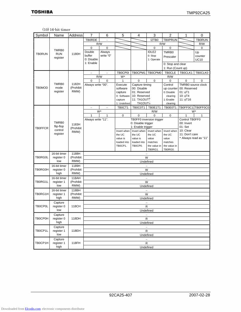
TMP92CA25
2007-02-28 92CA25-407
(10) 16-bit timer
Symbol Name Address 7 6 5 4 3 2 1 0 TB0RDE − I2TB0 TB0PRUN TB0RUN
R/W R/W R/W 0 0 0 0 0
TMRB0 Prescaler
Up counter UC10
TB0RUN TMRB0
RUN register
1180H Double buffer 0: Disable 1: Enable
Always write “0”
IDLE2 0: Stop 1: Operate
0: Stop and clear 1: Run (Count up)
− − TB0CP0I TB0CPM1 TB0CPM0 TB0CLE TB0CLK1 TB0CLK0R/W W* R/W
0 0 1 0 0 0 0 0
TB0MOD TMRB0 mode
register
1182H (Prohibit RMW)
Always write “00”. Execute software capture 0: Software capture 1: Undefined
Capture timing 00: Disable 01: Reserved 10: Reserved 11: TA1OUT↑ TA1OUT↓
Control up counter 0: Disable clearing 1: Enable clearing
TMRB0 source clock00: Reserved 01: φT1 10: φT4 11: φT16
− − TB0CT1 TB0C0T1 TB0E1T1 TB0E0T1 TB0FF0C1 TB0FF0C0W* R/W W*
1 1 0 0 0 0 1 1 TB0FF0 inversion trigger 0: Disable trigger 1: Enable trigger TB0FFCR
TMRB0 flip-flop control register
1183H (Prohibit RMW)
Always write “11”.
Invert when the UC value is loaded into TB0CP1.
Invert when the UC value is loaded into TB0CP0.
Invert when the UC value matches the value in TB0RG1.
Invert when the UC value matches the value in TB0RG0.
Control TB0FF0 00: Invert 01: Set 10: Clear 11: Don’t care * Always read as “11”
− W TB0RG0L
16-bit timer register 0
low
1188H (Prohibit RMW) Undefined
− W TB0RG0H
16-bit timer register 0
high
1189H (Prohibit RMW) Undefined
− W TB0RG1L
16-bit timer register 1
low
118AH (Prohibit RMW) Undefined
− W TB0RG1H
16-bit timer register 1
high
118BH (Prohibit RMW) Undefined
− R TB0CP0L
Capture register 0
low 118CH
Undefined − R TB0CP0H
Capture register 0
high 118DH
Undefined − R TB0CP1L
Capture register 1
low 118EH
Undefined − R TB0CP1H
Capture register 1
high 118FH
Undefined
Downloaded from Elcodis.com electronic components distributor

TMP92CA25
2007-02-28 92CA25-408
(11) UART/serial channel
Symbol Name Address 7 6 5 4 3 2 1 0 RB7 TB7
RB6 TB6
RB5 TB5
RB4 TB4
RB3 TB3
RB2 TB2
RB1 TB1
RB0 TB0
R (Receiving)/W (Transmission) SC0BUF
Serial channel 0
buffer register
1200H (Prohibit RMW)
Undefined RB8 EVEN PE OERR PERR FERR SCLKS IOC
R R/W R (Clear 0 after reading) R/W Undefined 0 0 0 0 0 0 0
1: Error SC0CR
Serial channel 0
control register
1201H Receive data bit8
Parity 0: Odd 1: Even
Parity 0: Disable1: Enable
Overrun Parity Framing 0: SCLK0↑ 1: SCLK0↓
0: Baud rate generator1: SCLK0 pin input
TB8 CTSE RXE WU SM1 SM0 SC1 SC0 R/W
0 0 0 0 0 0 0 0
SC0MOD0
Serial channel 0 mode 0 register
1202H Trans- mission data bit8
0: CTS disable
1: CTS enable
0: Receive disable
1: Receive enable
Wake-up0: Disable1: Enable
00: I/O Interface mode 01: 7-bit UART mode 10: 8-bit UART mode 11: 9-bit UART mode
00: TA0TRG 01: Baud rate generator 10: Internal clock fIO11: External clock (SCLK0 input)
− BR0ADDE BR0CK1 BR0CK0 BR0S3 BR0S2 BR0S1 BR0S0R/W
0 0 0 0 0 0 0 0 BR0CR
Serial channel 0 baud rate
control register
1203H Always write “0”
(16-K)/16 divided 0: Disable1: Enable
00: φT0 01: φT2 10: φT8 11: φT32
Set the frequency divisor “N” (0 to F)
BR0K3 BR0K2 BR0K1 BR0K0 R/W 0 0 0 0
BR0ADD
Serial channel 0 K setting register
1204H
Set the frequency divisor “K” (1 to F) I2S0 FDPX0
R/W 0 0
SC0MOD1
Serial channel 0 mode 1 register
1205H IDLE2 0: Stop 1: Operate
I/O interface mode 0: Half duplex
1: Full duplex
PLSEL RXSEL TXEN RXEN SIRWD3 SIRWD2 SIRWD1 SIRWD0R/W
0 0 0 0 0 0 0 0
SIRCR IrDA
control register
1207H Select transmit pulse width 0: 3/16 1: 1/16
Receive data 0: “H” pulse1: “L” pulse
Transmit0: Disable1: Enable
Receive 0: Disable1: Enable
Select receive pulse width Set effective pulse width for equal or more than 2x × (value + 1) + 100ns Can be set: 1 to 14 Can not be set: 0,15
Downloaded from Elcodis.com electronic components distributor
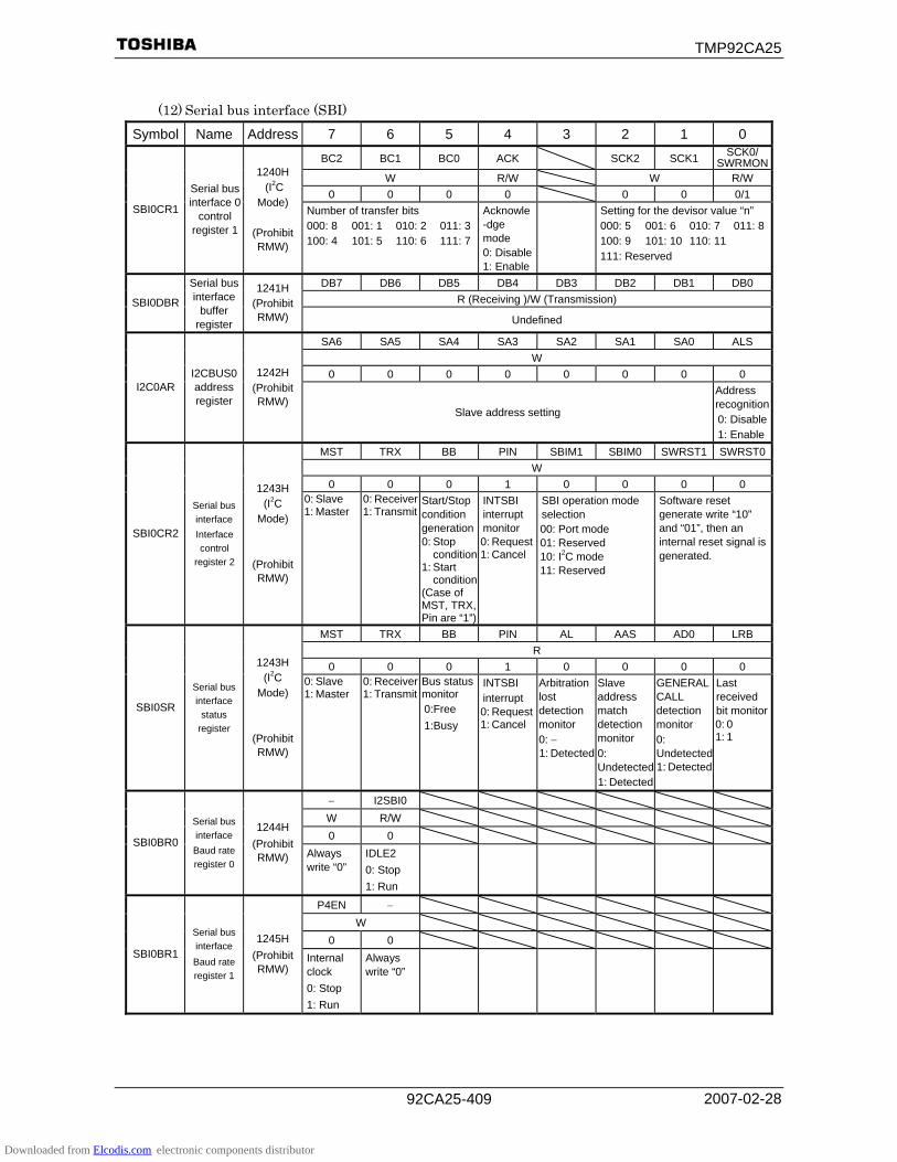
TMP92CA25
2007-02-28 92CA25-409
(12) Serial bus interface (SBI)
Symbol Name Address 7 6 5 4 3 2 1 0
BC2 BC1 BC0 ACK SCK2 SCK1 SCK0/ SWRMON
W R/W W R/W 0 0 0 0 0 0 0/1
SBI0CR1
Serial bus interface 0
control register 1
1240H (I2C
Mode)
(Prohibit RMW)
Number of transfer bits 000: 8 001: 1 010: 2 011: 3100: 4 101: 5 110: 6 111: 7
Acknowle-dge mode 0: Disable1: Enable
Setting for the devisor value “n” 000: 5 001: 6 010: 7 011: 8100: 9 101: 10 110: 11 111: Reserved
DB7 DB6 DB5 DB4 DB3 DB2 DB1 DB0 R (Receiving )/W (Transmission) SBI0DBR
Serial bus interface
buffer register
1241H (Prohibit RMW) Undefined
SA6 SA5 SA4 SA3 SA2 SA1 SA0 ALS W
0 0 0 0 0 0 0 0 I2C0AR
I2CBUS0 address register
1242H (Prohibit RMW)
Slave address setting
Address recognition0: Disable1: Enable
MST TRX BB PIN SBIM1 SBIM0 SWRST1 SWRST0W
0 0 0 1 0 0 0 0
SBI0CR2
Serial bus interface Interface control
register 2
1243H (I2C
Mode)
(Prohibit RMW)
0: Slave 1: Master
0: Receiver1: Transmit
Start/Stop condition generation0: Stop
condition1: Start
condition(Case of MST, TRX, Pin are “1”)
INTSBI interrupt monitor 0: Request1: Cancel
SBI operation mode selection 00: Port mode 01: Reserved 10: I2C mode 11: Reserved
Software reset generate write “10” and “01”, then an internal reset signal is generated.
MST TRX BB PIN AL AAS AD0 LRB R
0 0 0 1 0 0 0 0
SBI0SR
Serial bus interface
status register
1243H (I2C
Mode)
(Prohibit RMW)
0: Slave 1: Master
0: Receiver1: Transmit
Bus status monitor 0:Free 1:Busy
INTSBI interrupt 0: Request1: Cancel
Arbitration lost detection monitor 0: − 1: Detected
Slave address match detection monitor 0: Undetected 1: Detected
GENERAL CALL detection monitor 0: Undetected 1: Detected
Last received bit monitor0: 0 1: 1
− I2SBI0 W R/W 0 0 SBI0BR0
Serial bus interface Baud rate register 0
1244H (Prohibit RMW) Always
write “0” IDLE2 0: Stop 1: Run
P4EN − W
0 0 SBI0BR1
Serial bus interface Baud rate register 1
1245H (Prohibit RMW)
Internal clock 0: Stop 1: Run
Always write “0”
Downloaded from Elcodis.com electronic components distributor

TMP92CA25
2007-02-28 92CA25-410
(13)SPI controller (1/4) Symbol Name Address 7 6 5 4 3 2 1 0
XEN CLKSEL2 CLKSEL1 CLKSEL0
R/W R/W
0 1 0 0 Baud rate selection 0820H SYSCK
0: Disable1: Enable
000: fSYS 001: fSYS/2 010: fSYS/4 011: fSYS/8
100: fSYS/16 101: fSYS/32 110: fSYS/64 111: Reserved
LOOPBACK MSB1ST DOSTAT TCPOL RCPOL TDINV RDINV
R/W R/W
0 1 1 0 0 0 0
SPIMD SPI mode
setting register
0821HLOOPBACK test mode 0: Disable 1: Enable
Start bit for transmit
0: LSB
1: MSB
SPDO pin (No transmit)
0: Fixed to “0”
1: Fixed to “1”
Synchronous clock edge
during
transmitting
0: Falling
1: Rising
Synchronous clock edge
during
receiving
0: Falling
1: Rising
Invert data during
transmitting
0: Disable 1: Enable
Invert data during
receiving
0: Disable 1: Enable
CEN SPCS_B UNIT16 ALGNEN RXWEN RXUEN
R/W R/W 0 1 0 0 0 0
0822H Communication control 0: Disable 1: Enable
SPCS pin
0: Output “0”
1:Output “1”
Data length
0: 8bit
1: 16bit
Full duplex alignment 0: Disable 1: Enable
Sequential receive 0: Disable 1: Enable
Receive UNIT 0: Disable1: Enable
CRC16_7_B CRCRX_TX_B CRCRESET_B DMAERFW DMAERFR
R/W R/W
0 0 0 0 0
SPICT SPI control register
0823HCRC selection
0: CRC7
1: CRC16
CRC data
0: Transmit
1: Receive
CRC Calculation register
0:Reset
1:Relese reset
Micro DMA 0: Disable 1: Enable
Micro DMA 0: Disable1: Enable
TEND REND RFW RFR
R 1 0 1 0
0824H
Receiving
0: Operation
1: No operation
Receive shift t register
0: No data
1: Exist data
Transmit buffer
0: Exist un-transmitted data
1: No un-transmitted data
Receive buffer
0: No valid data
1: Exist valid data
SPIST SPI status register
0825H
Downloaded from Elcodis.com electronic components distributor

TMP92CA25
2007-02-28 92CA25-411
(13)SPI controller (2/4)
Symbol Name Address 7 6 5 4 3 2 1 0 CRCD7 CRCD6 CRCD5 CRCD4 CRCD3 CRCD2 CRCD1 CRCD0
R
0 0 0 0 0 0 0 0 0826H
CRC calculation result load register [7:0]
CRCD15 CRCD14 CRCD13 CRCD12 CRCD11 CRCD10 CRCD9 CRCD8
R
0 0 0 0 0 0 0 0
SPICR SPI CRC
register
0827H
CRC calculation result load register [15:8]
TENDIS RENDIS RFWIS RFRIS
R/W 0 0 0 0
0828H
Read
0:No interrupt
1:interrupt
Write
0:Don’t care
1:Clear
Read
0:No interrupt
1:interrupt
Write
0:Don’t care
1:Clear
Read
0:No interrupt
1:interrupt
Write
0:Don’t care
1:Clear
Read
0:No interrupt
1:interrupt
Write
0:Don’t care
1:Clear
SPIIS
SPI interrupt status
register
0829H
TENDWE RENDWE RFWWE RFRWE
R 0 0 0 0
082AH Clear SPIIS
<TENDIS>
0: Disable
1: Enable
Clear SPIIS
<RENDIS>
0: Disable
1: Enable
Clear SPIIS
<RFWIS>
0: Disable
1: Enable
Clear SPIIS
<RFRIS>
0: Disable
1: Enable
SPIWE
SPI interrupt
status write enable register
082BH
Downloaded from Elcodis.com electronic components distributor

TMP92CA25
2007-02-28 92CA25-412
(13) SPI controller (3/4) Symbol Name Address 7 6 5 4 3 2 1 0
TENDIE RENDIE RFWIE RFRIE
R/W
0 0 0 0 082CH TEND
interrupt
0: Disable 1: Enable
REND
interrupt
0: Disable
1: Enable
RFW
interrupt
0: Disable 1: Enable
RFR
interrupt
0: Disable
1: Enable
SPIIE
SPI interrupt enable register
082DH
TENDIR RENDIR RFWIR RFRIR
R 0 0 0 0
082EH TEND
interrupt
0: None
1: Generate
REND
interrupt
0: None
1: Generate
RFW
interrupt
0: None
1: Generate
RFR
interrupt
0: None
1: Generate
SPIIR
SPI interrupt request register
082FH
TXD7 TXD6 TXD5 TXD4 TXD3 TXD2 TXD1 TXD0
R/W 0 0 0 0 0 0 0 0
0830H
Transmission data register [7:0]
TXD15 TXD14 TXD13 TXD12 TXD11 TXD10 TXD9 TXD8
R/W
0 0 0 0 0 0 0 0
SPITD
SPI transmissio
n data register
0831H
Transmission data register [15:8]
Downloaded from Elcodis.com electronic components distributor

TMP92CA25
2007-02-28 92CA25-413
(13) SPI controller (4/4)
Symbol Name Address 7 6 5 4 3 2 1 0 RXD7 RXD6 RXD5 RXD4 RXD3 RXD2 RXD1 RXD0
R
0 0 0 0 0 0 0 0 0832H
Receive data register [7:0]
RXD15 RXD14 RXD13 RXD12 RXD11 RXD10 RXD9 RXD8
R
0 0 0 0 0 0 0 0
SPIRD SPI receive register
0833H
Receive data register [15:8]
TSD7 TSD6 TSD5 TSD4 TSD3 TSD2 TSD1 TSD0
R 0 0 0 0 0 0 0 0
0834H
Transmission data shift register [7:0]
TSD15 TSD14 TSD13 TSD12 TSD11 TSD10 TSD9 TSD8
R
0 0 0 0 0 0 0 0
SPITS
SPI transmission
data shift register
0835H
Transmission data register [15:8]
RSD7 RSD6 RSD5 RSD4 RSD3 RSD2 RSD1 RSD0
R 0 0 0 0 0 0 0 0
0836H
RSD15 RSD14 RSD13 RSD12 RSD11 RSD10 RSD9 RSD8
R/W
0 0 0 0 0 0 0 0
SPIRS SPI receive
data register
0837H
Downloaded from Elcodis.com electronic components distributor

TMP92CA25
2007-02-28 92CA25-414
(14) AD converter (1/2)
Symbol Name Address 7 6 5 4 3 2 1 0 EOCF ADBF − − ITM0 REPEAT SCAN ADS
R R/W 0 0 0 0 0 0 0 0
ADMOD0 AD mode
control register 0
12B8H
AD conversion end flag 1:END
AD conversionBUSY flag1: Busy
Always write “0”
Always write “0”
0: Every 1 time 1: Every 4 times
Repeat mode 0: Single
mode 1: Repeat
mode
Scan mode 0: Fixed channel mode 1: Channel
scan mode
AD conversion start
1: Start always read as “0”
VREFON I2AD − − − − ADCH1 ADCH0R/W R/W R/W
0 0 0 0 0 0 0 0
ADMOD1 AD mode
control register 1
12B9H Ladder resistance 0: OFF 1: ON
IDLE2 0: Stop 1: Operate
Always write “0”
Always write “0”
Always write “0”
Always write “0”
Input channel 000: AN0 001: AN1 010: AN2 011: AN3
− − − − − − − ADTRGR/W
0 0 0 0 0 0 0 0
ADMOD2 AD mode
control register 1
12BAH Always write “0”
Always write “0”
Always write “0”
Always write “0”
Always write “0”
Always write “0”
Always write “0”
AD external
trigger startcontrol 0: Disable1: Enable
ADR01 ADR00 ADR0RFR R ADREG0L
AD result register 0
low 12A0H
Undefined 0 ADR09 ADR08 ADR07 ADR06 ADR05 ADR04 ADR03 ADR02
R ADREG0H AD result register 0
high 12A1H
Undefined ADR11 ADR10 ADR1RF
R R ADREG1L AD result register 1
low 12A2H
Undefined 0 ADR19 ADR18 ADR17 ADR16 ADR15 ADR14 ADR13 ADR12
R ADREG1H AD result register 1
high 12A3H
Undefined ADR21 ADR20 ADR2RF
R R ADREG2L AD result register 2
low 12A4H
Undefined 0 ADR29 ADR28 ADR27 ADR26 ADR25 ADR24 ADR23 ADR22
R ADREG2H AD result register 2
high 12A5H
Undefined ADR31 ADR30 ADR3RF
R R ADREG3L AD result register 3
low 12A6H
Undefined 0 ADR39 ADR38 ADR37 ADR36 ADR35 ADR34 ADR33 ADR32
R ADREG3H AD result register 3
high 12A7H
Undefined
Downloaded from Elcodis.com electronic components distributor

TMP92CA25
2007-02-28 92CA25-415
(15) Watchdog timer
Symbol Name Address 7 6 5 4 3 2 1 0 WDTE WDTP1 WDTP0 − I2WDT RESCR −
R/W R/W 1 0 0 0 0 0 0
WDMOD WDT mode
register 1300H WDT
control 1: Enable
Select detecting time00: 215/fIO 01: 217/fIO 10: 219/fIO 11: 221/fIO
Always write “0”
IDLE2 0: Stop 1: Operate
1: Internally connects
WDT out
to the reset pin
Always write “0”
− W −
WDCR WDT
control register
1301H (Prohibit RMW)
B1H: WDT disable code 4E: WDT clear code
Downloaded from Elcodis.com electronic components distributor
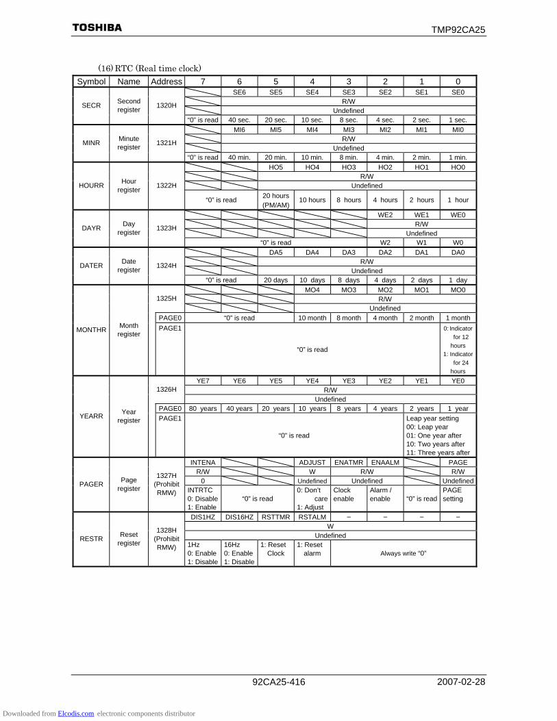
TMP92CA25
2007-02-28 92CA25-416
(16) RTC (Real time clock)
Symbol Name Address 7 6 5 4 3 2 1 0 SE6 SE5 SE4 SE3 SE2 SE1 SE0 R/W Undefined
SECR Second register 1320H
“0” is read 40 sec. 20 sec. 10 sec. 8 sec. 4 sec. 2 sec. 1 sec. MI6 MI5 MI4 MI3 MI2 MI1 MI0 R/W Undefined
MINR Minute register 1321H
“0” is read 40 min. 20 min. 10 min. 8 min. 4 min. 2 min. 1 min. HO5 HO4 HO3 HO2 HO1 HO0 R/W Undefined HOURR Hour
register 1322H
“0” is read 20 hours(PM/AM)
10 hours 8 hours 4 hours 2 hours 1 hour
WE2 WE1 WE0 R/W Undefined
DAYR Day register 1323H
“0” is read W2 W1 W0 DA5 DA4 DA3 DA2 DA1 DA0 R/W Undefined
DATER Date register 1324H
“0” is read 20 days 10 days 8 days 4 days 2 days 1 day MO4 MO3 MO2 MO1 MO0 R/W 1325H Undefined
PAGE0 “0” is read 10 month 8 month 4 month 2 month 1 month
MONTHR Month register
PAGE1
“0” is read
0: Indicator for 12
hours 1: Indicator
for 24 hours
YE7 YE6 YE5 YE4 YE3 YE2 YE1 YE0 R/W 1326H
Undefined PAGE0 80 years 40 years 20 years 10 years 8 years 4 years 2 years 1 year
YEARR Year register
PAGE1
“0” is read
Leap year setting 00: Leap year 01: One year after 10: Two years after 11: Three years after
INTENA ADJUST ENATMR ENAALM PAGE R/W W R/W R/W
0 Undefined Undefined UndefinedPAGER Page register
1327H (Prohibit RMW) INTRTC
0: Disable 1: Enable
“0” is read 0: Don’t
care1: Adjust
Clock enable
Alarm / enable “0” is read
PAGE setting
DIS1HZ DIS16HZ RSTTMR RSTALM − − − − W
Undefined RESTR Reset register
1328H (Prohibit RMW) 1Hz
0: Enable 1: Disable
16Hz 0: Enable1: Disable
1: Reset Clock
1: Reset alarm Always write “0”
Downloaded from Elcodis.com electronic components distributor
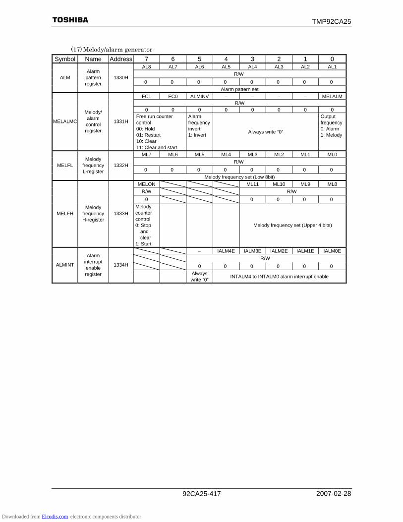
TMP92CA25
2007-02-28 92CA25-417
(17) Melody/alarm generator
Symbol Name Address 7 6 5 4 3 2 1 0 AL8 AL7 AL6 AL5 AL4 AL3 AL2 AL1
R/W 0 0 0 0 0 0 0 0
ALM Alarm pattern register
1330H
Alarm pattern set FC1 FC0 ALMINV − − − − MELALM
R/W 0 0 0 0 0 0 0 0
MELALMC
Melody/ alarm control register
1331HFree run counter control 00: Hold 01: Restart 10: Clear 11: Clear and start
Alarm frequency invert 1: Invert Always write “0”
Output frequency 0: Alarm 1: Melody
ML7 ML6 ML5 ML4 ML3 ML2 ML1 ML0 R/W
0 0 0 0 0 0 0 0 MELFL
Melody frequency L-register
1332H
Melody frequency set (Low 8bit) MELON ML11 ML10 ML9 ML8
R/W R/W 0 0 0 0 0
MELFH Melody
frequency H-register
1333HMelody counter control 0: Stop
and clear
1: Start
Melody frequency set (Upper 4 bits)
− IALM4E IALM3E IALM2E IALM1E IALM0E R/W 0 0 0 0 0 0 ALMINT
Alarm interrupt enable register
1334H
Always write “0” INTALM4 to INTALM0 alarm interrupt enable
Downloaded from Elcodis.com electronic components distributor
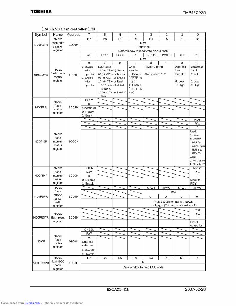
TMP92CA25
2007-02-28 92CA25-418
(18) NAND flash controller (1/2)
Symbol Name Address 7 6 5 4 3 2 1 0 D7 D6 D5 D4 D3 D2 D1 D0
R/W Undefined
ND0FDTR
NAND flash data transfer register
1D00H
Data window to read/write NAND flash WE ECC1 ECC0 CE PCNT1 PCNT0 ALE CLE
R/W 0 0 0 0 0 0 0 0
ND0FMCR
NAND flash mode
control register
1CC4H
0: Disable write operation
1: Enable write operation
ECC circuit 11 (at <CE>=X): Reset 00 (at <CE>=1): Disable01 (at <CE>=1): Enable10 (at <CE>=1): Read
ECC data calculated by NDFC
10 (at <CE>=0): Read ID data
Chip enable 0: Disable( NDCE is high) 1: Enable( NDCE is low)
Power Control Always write “11”
Address Latch Enable 0: Low 1: High
Command Latch Enable 0: Low 1: High
BUSY R
Undefined ND0FSR
NAND flash status
register
1CC8H 0: Ready 1: Busy
RDY R/W 0
ND0FISR
NAND flash
interrupt status
register
1CCCH
Read: 0: None 1: Change
NDR/ B signal from BUSY to READY.
Write: 0: No change1: Clear to “0”
INTEN MRDY R/W R/W
0 0 ND0FIMR
NAND flash
interrupt mask
register
1CD0H 0: Disable 1: Enable
Mask for RDY
SPW3 SPW2 SPW1 SPW0 R/W 0 0 0 0 ND0FSPR
NAND flash
strobe pulse width
register
1CD4H
Pulse width for NDRE , NDWE = fSYS × (This register’s value + 1)
RST R/W 0 ND0FRSTR
NAND flash reset
register 1CD8H
Reset controller
CHSEL R/W
0 NDCR
NAND flash
control register
01C0H Channel selection 0: Channel 0
1: Channel 1
D7 D6 D5 D4 D3 D2 D1 D0 R ND0ECCRD
NAND flash ECC
code register
1CB0H Data window to read ECC code
Downloaded from Elcodis.com electronic components distributor

TMP92CA25
2007-02-28 92CA25-419
(17) NAND flash controller (2/2)
Symbol Name Address 7 6 5 4 3 2 1 0 D7 D6 D5 D4 D3 D2 D1 D0
R/W Undefined
ND1FDTR
NAND flash data transfer register
1D00H
Data window to read/write NAND flash WE ECC1 ECC0 CE PCNT1 PCNT0 ALE CLE
R/W 0 0 0 0 0 0 0 0
ND1FMCR
NAND flash mode control register
1CE4H
0: Disable write operation
1: Enable write operation
ECC circuit 11 (at <CE>=X): Reset 00 (at <CE>=1): Disable01 (at <CE>=1): Enable10 (at <CE>=1): Read
ECC data calculated by NDFC
10 (at <CE>=0): Read ID data
Chip enable 0: Disable( NDCE is high) 1: Enable( NDCE is low)
Power Control Always write “11”
Address Latch Enable 0: Low 1: High
Command Latch Enable 0: Low 1: High
BUSY R
Undefined ND1FSR
NAND flash status
register
1CE8H 0: Ready 1: Busy
RDY R/W 0
ND1FISR
NAND flash
interrupt status
register
1CECH
Read: 0: None 1: Change
NDR/ B signal from BUSY to READY.
Write: 0: No change1: Clear to “0”
INTEN MRDY R/W R/W
0 0 ND1FIMR
NAND flash
interrupt mask
register
1CF0H 0: Disable 1: Enable
Mask for RDY
SPW3 SPW2 SPW1 SPW0 R/W 0 0 0 0 ND1FSPR
NAND flash
strobe pulse width
register
1CF4H Pulse width for NDRE , NDWE
= fSYS × (This register’s value +1)
RST R/W 0 ND1FRSTR
NAND flash reset
register 1CF8H
Reset controller
D7 D6 D5 D4 D3 D2 D1 D0 R ND1ECCRD
NAND flash ECC
code register
1CB0H Data window to read ECC code
Downloaded from Elcodis.com electronic components distributor

TMP92CA25
2007-02-28 92CA25-420
(19) I2S
Symbol Name Address 7 6 5 4 3 2 1 0 R15/R7 R14/R6 R13/R5 R12/R4 R11/R3 R10/R2 R9/R1 R8/R0
W Undefined
I2SBUFR I2S FIFO buffer (R)
0800H (Prohibit RMW)
Register for transmitting buffer (FIFO) (Right channel) L15/L7 L14/L6 L13/L5 L12/L4 L11/L3 L10/L2 L9/L1 L8/L0
W Undefined
I2SBUFL I2S FIFO buffer (L)
0808H (Prohibit RMW)
Register for transmitting buffer (FIFO) (Left channel) TXE FMT BUSY DIR BIT MCK1 MCK0 I2SWCK
R/W R R/W 0 0 0 0 0 0 0 0
080EH Transmit 0: Stop 1: Start
Mode 0: I2S 1: SIO
Status 0: Stop 1: Under
transmitting
First bit 0: MSB 1: LSB
Bit number 0: 8 bits 1: 16 bits
Baud rate 00: fSYS 10: fSYS/4 01: fSYS/2 11: fSYS/8
WS clock0: fs/4 1: TA1OUT
I2SWLVL EDGE I2SFSEL I2SCKE SYSCKER/W R/W
0 0 0 0 0
I2SCTL0 I2S
control register 0
080FH WS level 0: Low left 1: High left
Clock edge 0: Falling1: Rising
Select for stereo 0: Stereo
(2 channel)
1: Monaural(1 channel)
Clock enable (After transmit)0: Operation
1: Stop
System clock 0: Disable1: Enable
Downloaded from Elcodis.com electronic components distributor
TMP92CA25
2007-02-28 92CA25-421
6. Notes and Restrictions
6.1 Notation
(1) The notation for built-in I/O registers is as follows: Register symbol <Bit symbol> Example: TA01RUN<TA0RUN> denotes bit TA0RUN of register TA01RUN.
(2) Read-modify-write instructions (RMW) An instruction in which the CPU reads data from memory and writes the data to the
same memory location in one instruction. Example 1: SET 3, (TA01RUN); Set bit3 of TA01RUN. Example 2: INC 1, (100H); Increment the data at 100H.
• Examples of read-modify-write instructions on the TLCS-900 Exchange instruction
EX (mem), R
Arithmetic operations ADD (mem), R/# ADC (mem), R/# SUB (mem), R/# SBC (mem), R/# INC #3, (mem) DEC #3, (mem)
Logic operations
AND (mem), R/# OR (mem), R/# XOR (mem), R/#
Bit manipulation operations
STCF #3/A, (mem) RES #3, (mem) SET #3, (mem) CHG #3, (mem) TSET #3, (mem)
Rotate and shift operations
RLC (mem) RRC (mem) RL (mem) RR (mem) SLA (mem) SRA (mem) SLL (mem) SRL (mem) RLD (mem) RRD (mem)
(3) fOSCH, fc, fFPH, fSYS, fIO and one state The clock frequency input on pins X1 and 2 is referred to as fOSCH. The clock selected by
PLLCR0<FCSEL> is referred as fc.
The clock selected by SYSCR1<SYSCK> is refer to as fFPH. The clock frequency give by fFPH divided by 2 is referred to as system clock fSYS. The clock frequency give by fSYS divided by 2 is referred to as fIO.
One cycle of fSYS is referred to as one state.
Downloaded from Elcodis.com electronic components distributor

TMP92CA25
2007-02-28 92CA25-422
6.2 Notes
(1) AM0 and AM1 pins These pins are connected to the VCC (Power supply level) or the VSS (Grand level) pin.
Do not alter the level when the pin is active.
(2) Reserved address areas The 16 bytes area (FFFFF0H ∼ FFFFFFH) cannot be used since it is reserved for use as
internal area. If using an emulator, an optional 64 Kbytes of the 16M bytes area is used for emulator control. Therefore, if using an emulator, this area cannot be used.
(3) Standby mode (IDLE1) When the HALT instruction is executed in IDLE1 mode (in which only the oscillator
operates), the internal RTC (Real-time-clock) and MLD (Melody-alarm-generator) operate. When necessity, stop the circuit before the HALT instruction is executed.
(4) Warm-up counter The warm-up counter operates when STOP mode is released, even if the system is using
an external oscillator. As a result, a time equivalent to the warm-up time elapses between input of the release request and output of the system clock.
(5) Watchdog timer The watchdog timer starts operation immediately after a reset is released. Disable the
watchdog timer when is not to be used.
(6) AD converter The string resistor between the VREFH and VREFL pins can be cut by program so as to
reduce power consumption. When STOP mode is used, disable the resistor using the program before the HALT instruction is executed.
(7) CPU (Micro DMA) Only the “LDC cr, r” and “LDC r, cr” instructions can be used to access the control
registers in the CPU. (e.g., the transfer source address register (DMASn).)
(8) Undefined SFR The value of an undefined bit in an SFR is undefined when read.
(9) POP SR instruction Please execute the POP SR instruction during DI condition.
Downloaded from Elcodis.com electronic components distributor
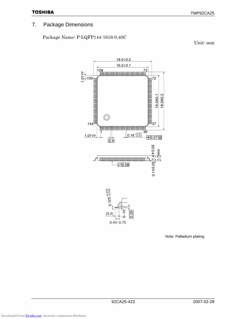
TMP92CA25
2007-02-28 92CA25-423
7. Package Dimensions
Package Name: P-LQFP144-1616-0.40C Unit: mm
Note: Palladium plating
Downloaded from Elcodis.com electronic components distributor

TMP92CA25
2007-02-28 92CA25-424
Downloaded from Elcodis.com electronic components distributor