
TLV320AIC3254EVM-K - User Guide (Rev. A) - Texas … · EVM Overview 1 EVM Overview 1.1 Features...
54
User's Guide SLAU264A – October 2008 – Revised September 2012 TLV320AIC3254EVM-K This user's guide describes the characteristics, operation, and use of the TLV320AIC3254EVM-K. This evaluation module (EVM) features a complete stereo audio codec with several inputs and outputs, extensive audio routing, mixing, and effects capabilities. A complete circuit description, schematic diagram, and bill of materials are also included. The following related documents are available through the Texas Instruments Web site at www.ti.com. EVM-Compatible Device Data Sheets Device Literature Number TLV320AIC3254 SLAS549 TAS1020B SLES025 REG1117-3.3 SBVS001 TPS767D318 SLVS209 SN74LVC125A SCAS290 SN74LVC1G125 SCES223 SN74LVC1G07 SCES296 Contents 1 EVM Overview ............................................................................................................... 3 2 EVM Description and Basics .............................................................................................. 3 3 TLV320AIC3254EVM-K Setup and Installation ......................................................................... 7 4 AIC3254 Control Software ............................................................................................... 11 Appendix A EVM Connector Descriptions ................................................................................... 26 Appendix B TLV320AIC3254EVM Schematic ............................................................................... 30 Appendix C TLV320AIC3254EVM Layout Views ........................................................................... 31 Appendix D TLV320AIC3254EVM Bill of Materials ......................................................................... 35 Appendix E USB-MODEVM Schematic ...................................................................................... 38 Appendix F USB-MODEVM Bill of Materials ................................................................................ 39 Appendix G USB-MODEVM Protocol ......................................................................................... 41 List of Figures 1 TLV320AIC3254EVM-K Block Diagram ................................................................................. 4 2 Initial Screen of TLV320AIC3254EVM-K Software ..................................................................... 9 3 Compatibility Tab .......................................................................................................... 10 4 Playback Script Tab ....................................................................................................... 12 5 Playback Panel ............................................................................................................ 13 6 Recording Panel ........................................................................................................... 14 7 DRC Information Tab ..................................................................................................... 15 8 Program Codec Pop-Up Window........................................................................................ 15 PowerTune is a trademark of Texas Instruments. I 2 S, I 2 C are trademarks of Koninklijke Philips Electronics N.V. Windows is a trademark of Microsoft Corporation. SPI is a trademark of Motorola, Inc. I 2 C is a trademark of Philips Corporation. is a trademark of ~ Texas Instruments, Inc.. 1 SLAU264A – October 2008 – Revised September 2012 TLV320AIC3254EVM-K Submit Documentation Feedback Copyright © 2008–2012, Texas Instruments Incorporated
Transcript of TLV320AIC3254EVM-K - User Guide (Rev. A) - Texas … · EVM Overview 1 EVM Overview 1.1 Features...
User's GuideSLAU264A–October 2008–Revised September 2012
TLV320AIC3254EVM-K
This user's guide describes the characteristics, operation, and use of the TLV320AIC3254EVM-K. Thisevaluation module (EVM) features a complete stereo audio codec with several inputs and outputs,extensive audio routing, mixing, and effects capabilities. A complete circuit description, schematicdiagram, and bill of materials are also included.
The following related documents are available through the Texas Instruments Web site at www.ti.com.
EVM-Compatible Device Data Sheets
Device Literature Number
TLV320AIC3254 SLAS549
TAS1020B SLES025
REG1117-3.3 SBVS001
TPS767D318 SLVS209
SN74LVC125A SCAS290
SN74LVC1G125 SCES223
SN74LVC1G07 SCES296
Contents1 EVM Overview ............................................................................................................... 32 EVM Description and Basics .............................................................................................. 33 TLV320AIC3254EVM-K Setup and Installation ......................................................................... 74 AIC3254 Control Software ............................................................................................... 11Appendix A EVM Connector Descriptions ................................................................................... 26Appendix B TLV320AIC3254EVM Schematic ............................................................................... 30Appendix C TLV320AIC3254EVM Layout Views ........................................................................... 31Appendix D TLV320AIC3254EVM Bill of Materials ......................................................................... 35Appendix E USB-MODEVM Schematic ...................................................................................... 38Appendix F USB-MODEVM Bill of Materials ................................................................................ 39Appendix G USB-MODEVM Protocol ......................................................................................... 41
List of Figures
1 TLV320AIC3254EVM-K Block Diagram ................................................................................. 4
2 Initial Screen of TLV320AIC3254EVM-K Software ..................................................................... 9
3 Compatibility Tab .......................................................................................................... 10
4 Playback Script Tab ....................................................................................................... 12
5 Playback Panel ............................................................................................................ 13
6 Recording Panel ........................................................................................................... 14
7 DRC Information Tab ..................................................................................................... 15
8 Program Codec Pop-Up Window........................................................................................ 15
PowerTune is a trademark of Texas Instruments.I2S, I2C are trademarks of Koninklijke Philips Electronics N.V.Windows is a trademark of Microsoft Corporation.SPI is a trademark of Motorola, Inc.I2C is a trademark of Philips Corporation.is a trademark of ~ Texas Instruments, Inc..
1SLAU264A–October 2008–Revised September 2012 TLV320AIC3254EVM-KSubmit Documentation Feedback
Copyright © 2008–2012, Texas Instruments Incorporated
www.ti.com
9 Adaptive Filtering Panel .................................................................................................. 16
10 Automatic Gain Control Panel ........................................................................................... 17
11 Dynamic Range Compression Panel ................................................................................... 18
12 Headset Detection Panel ................................................................................................. 19
13 DC Measurement Panel .................................................................................................. 20
14 Equalizers miniDSP Application ......................................................................................... 21
15 Spectrum Analyzer ........................................................................................................ 22
16 Audio Inputs Panel ........................................................................................................ 22
17 Status Flags Panel ........................................................................................................ 23
18 Register Tables Panel .................................................................................................... 24
19 Command-line Interface Panel .......................................................................................... 25
20 Top Layer................................................................................................................... 31
21 Mid-Layer 1................................................................................................................. 31
22 Mid-Layer 2................................................................................................................. 32
23 Bottom Layer ............................................................................................................... 32
24 Top Overlay ................................................................................................................ 33
25 Bottom Overlay ............................................................................................................ 33
26 Drill Drawing................................................................................................................ 34
27 Composite .................................................................................................................. 34
List of Tables
1 USB-MODEVM SW2 Settings............................................................................................. 5
2 List of Jumpers and Switches ............................................................................................. 5
3 Analog Interface Pinout................................................................................................... 26
4 Alternate Analog Connectors ............................................................................................ 27
5 Digital Interface Pinout.................................................................................................... 28
6 Power Supply Pin Out .................................................................................................... 29
7 TLV320AIC3254EVM Bill of Materials .................................................................................. 35
8 USB-MODEVM Bill of Materials ......................................................................................... 39
9 USB Control Endpoint HIDSETREPORT Request.................................................................... 41
10 Data Packet Configuration ............................................................................................... 41
11 GPIO Pin Assignments ................................................................................................... 44
2 TLV320AIC3254EVM-K SLAU264A–October 2008–Revised September 2012Submit Documentation Feedback
Copyright © 2008–2012, Texas Instruments Incorporated

www.ti.com EVM Overview
1 EVM Overview
1.1 Features• Full-featured evaluation board for the TLV320AIC3254 stereo audio codec.
• USB connection to PC provides power, control, and streaming audio data for easy evaluation.
• Onboard microphone for ADC evaluation
• Connection points for external control and digital audio signals for quick connection to othercircuits/input devices.
The TLV320AIC3254EVM-K is a complete evaluation kit, which includes a universal serial bus (USB)-based motherboard and evaluation software for use with a personal computer running the MicrosoftWindows™ operating system (Win2000 or XP).
1.2 Introduction
The TLV320AIC3254EVM is in the Texas Instruments (TI) modular EVM form factor, which allows directevaluation of the device performance and operating characteristics and eases software development andsystem prototyping.
The TLV320AIC3254EVM-K is a complete evaluation/demonstration kit, which includes a USB-basedmotherboard called the USB-MODEVM Interface board and evaluation software for use with a personalcomputer (PC) running the Microsoft Windows operating systems.
The TLV320AIC3254EVM-K is operational with one USB cable connection to a PC. The USB connectionprovides power, control, and streaming audio data to the EVM for reduced setup and configuration. TheEVM also allows external control signals, audio data, and power for advanced operation, which allowsprototyping and connection to the rest of the development or system evaluation.
2 EVM Description and Basics
This section provides information on the analog input and output, digital control, power, and generalconnection of the TLV320AIC3254EVM-K.
2.1 TLV320AIC3254EVM-K Block Diagram
The TLV320AIC3254EVM-K consists of two separate circuit boards, the USB-MODEVM and theTLV320AIC3254EVM. The USB-MODEVM is built around the TAS1020B streaming audio USB controllerwith an 8051-based core. The motherboard features two positions for modular EVMs, or one double-wideserial modular EVM can be installed. The TLV320AIC3254EVM is one of the double-wide modular EVMsthat is designed to work with the USB-MODEVM.
The simple diagram of Figure 1 shows how the TLV320AIC3254EVM is connected to the USB-MODEVM.The USB-MODEVM Interface board is intended to be used in USB mode, where control of the installedEVM is accomplished using the onboard USB controller device. Provision is made, however, for driving allthe data buses ( I2C™, SPI™, I2S, etc.) externally. The source of these signals is controlled by SW2 onthe USB-MODEVM. See Table 1 for details on the switch settings.
The USB-MODEVM has two EVM positions that allow for the connection of two small evaluation moduleor one larger evaluation module. The TLV320AIC3254EVM is designed to fit over both of the smallerevaluation module slots as shown in Figure 1
3SLAU264A–October 2008–Revised September 2012 TLV320AIC3254EVM-KSubmit Documentation Feedback
Copyright © 2008–2012, Texas Instruments Incorporated

EVM Position 2
EVM Position 1
TLV320AIC32x4EVM
Control Interface
TLV320AIC32x4
TAS1020B
USB 8051
Microcontroller
USB
SPI, I C2
I S, AC972
Audio Interface
USB-MODEVM
EVM Description and Basics www.ti.com
2.1.1 USB-MODEVM Interface Board
The simple diagram of Figure 1 shows only the basic features of the USB-MODEVM Interface board.
Because the TLV320AIC3254EVM is a double-wide modular EVM, it is installed with connections to bothEVM positions, which connects the TLV320AIC3254 digital control interface to the I2C port realized usingthe TAS1020B, as well as the TAS1020B digital audio interface.
In the factory configuration, the board is ready to be used with the USB-MODEVM. To view all thefunctions and configuration options available on the USB-MODEVM board, see the USB-MODEVMInterface Board schematic in Appendix G.
Figure 1. TLV320AIC3254EVM-K Block Diagram
4 TLV320AIC3254EVM-K SLAU264A–October 2008–Revised September 2012Submit Documentation Feedback
Copyright © 2008–2012, Texas Instruments Incorporated

www.ti.com EVM Description and Basics
2.2 Default Configuration and Connections
2.2.1 USB-MODEVM
Table 1 provides a list of the SW2 settings on the USB-MODEVM. For use with the TLV320AIC3254EVM,SW-2 positions 1, 3, 4, 5, 6, and 7 must be set to ON, whereas SW-2.2 and SW-2.8 must be set to OFF. Ifthe TLV320AIC3254EVM is to be used with an external audio interface, SW2.4 and SW2.5 also need tobe set to OFF and such interface must be connected as explained in Section 2.4
Table 1. USB-MODEVM SW2 Settings
SW-2 Switch Number Label Switch Description
1 A0 USB-MODEVM EEPROM I2C Address A0ON: A0 = 0OFF: A0 = 1
2 A1 USB-MODEVM EEPROM I2C Address A1ON: A1 = 0OFF: A1 = 1
3 A2 USB-MODEVM EEPROM I2C Address A2ON: A2 = 0OFF: A2 = 1
4 USB I2S I2S Bus Source SelectionON: I2S Bus connects to TAS1020OFF: I2S Bus connects to USB-MODEVM J14
5 USB MCK I2S Bus MCLK Source SelectionON: MCLK connects to TAS1020OFF: MCLK connects to USB-MODEVM J14
6 USB SPI SPI Bus Source SelectionON: SPI Bus connects to TAS1020OFF: SPI Bus connects to USB-MODEVM J15
7 USB RST RST Source SelectionON: EVM Reset Signal comes from TAS1020OFF: EVM Reset Signal comes from USB-MODEVM J15
8 EXT MCK External MCLK SelectionON: MCLK Signal is provided from USB-MODEVM J10OFF: MCLK Signal comes from either selection of SW2-5
2.2.2 TLV320AIC3254 Jumper Locations
Table 2 provides a list of jumpers found on the EVM and their factory default conditions.
Table 2. List of Jumpers and Switches
DefaultJumper Position Jumper Description
W1 2-3 When connecting 2-3, microphone bias comes from the MICBIAS pin on the device; when connecting 1-2, microphone (mic) bias issupplied through TP8.
W2 Installed Connects onboard Mic negative terminal to the circuit.
W3 Installed Connects onboard Mic positive terminal to the circuit.
W4 Open Provides mic bias to J5.3 (disconnect W2 and W3 before installing this jumper). Use for stereo electret microphones only.
W5 Installed Provides mic bias to J5.2 and onboard Mic positive terminal.
W6 Installed Sets the mic bias resistance to 1 kΩ. Use for differential electret mic configurations.
W7 Installed Connects J5.3 and onboard Mic negative terminal to the circuit.
W8 2-3 Connects J5.3 and onboard Mic negative terminal to AVSS or 1-kΩ resistor.
W9 Open Connects 16-Ω load to HPL outputs.
W10 Open Connects 16-Ω load to HPR outputs.
W11 Open When installed, shorts across the output capacitor on HPL; remove this jumper if using AC-coupled output drive
W12 Open When installed, shorts across the output capacitor on HPR; remove this jumper if using AC-coupled output drive
W13 Installed When installed, it selects onboard EEPROM as firmware source.
W14 1-2 When set to 1-2, SCLK/MIC_DET is used for SPI SCLK. When set to 2-3, SCLK/MIC_DET is used for headset detection.
5SLAU264A–October 2008–Revised September 2012 TLV320AIC3254EVM-KSubmit Documentation Feedback
Copyright © 2008–2012, Texas Instruments Incorporated
EVM Description and Basics www.ti.com
Table 2. List of Jumpers and Switches (continued)
DefaultJumper Position Jumper Description
W15 Open When installed, connects GPIO4 to reset AND gate (U3).
W16 Installed Provides a means of measuring IOVDD current.
W17 Installed Provides a means of measuring DVDD current.
W18 Installed Provides a means of measuring LDOin/HPVDD current. ???
W19 Installed Provides a means of measuring AVDD current.
W20 2-3 Sets U6 voltage source as +5VD or +5VA for LDOin/HPVDD.
W21 Installed Connects +3.3VD voltage source to IOVDD node.
W22 Open When installed, shorts across the input capacitor on IN2_L for DC measurement option. Remove this jumper for audio connections.
W23 Open When installed, shorts across the input capacitor on IN2_R for DC measurement option. Remove this jumper for audio connections.
SW1 I2C When set to I2C, the I2C signals from P12/J12 are connected to the codec and SPI_SELECT is set low. When set to SPI, the SPIsignals from P12/J12 are connected to the codec and SPI_SELECT is pulled to IOVDD.
SW2 LOW When set to LOW, AVDD and DVDD are connected to +1.8VA and +1.8VD, respectively, and LDO_SELECT is set low. When set toHI, AVDD, and DVDD are disconnected from other supplies and LDO_SELECT is pulled to IOVDD.
2.3 Analog Signal Connections
2.3.1 Analog Inputs
The analog input sources can be applied directly to terminal blocks J2, J3, and J4 or input jacks J1 andJ5. The connection details can be found in Appendix A.
2.3.2 Analog Output
The analog outputs are available from terminal blocks J6 and J8 or output jacks J7, J9, and J10. Note thatJ10 is provided for signal-to-noise ratio (SNR) measurements only. The connection details can be found inAppendix A.
2.4 Digital Signal Connections
The digital inputs and outputs of the EVM can be monitored through P12 and P22. If external signals needto be connected to the EVM, digital inputs must be connected via J14 and J15 on the USB-MODEVM andthe SW2 switch must be changed accordingly (see Section 2.2.1). The connector details are available inSection A.2.
2.5 Power Connections
The TLV320AIC3254EVM can be powered independently when being used in stand-alone operation or bythe USB-MODEVM when it is plugged onto the motherboard.
6 TLV320AIC3254EVM-K SLAU264A–October 2008–Revised September 2012Submit Documentation Feedback
Copyright © 2008–2012, Texas Instruments Incorporated

www.ti.com TLV320AIC3254EVM-K Setup and Installation
2.5.1 Stand-Alone Operation
When used as a stand-alone EVM, power is applied to P23/J23 directly, making sure to reference thesupplies to the appropriate grounds on that connector.
CAUTION
Verify that all power supplies are within the safe operating limits shown on theTLV320AIC3254 data sheet before applying power to the EVM.
P23/J23 provides connection to the common power bus for the TLV320AIC3254EVM. Power is suppliedon the pins listed in Table 6.
The TLV320AIC3254EVM-K motherboard (the USB-MODEVM Interface board) supplies power to P23/J23of the TLV320AIC3254EVM. Power for the motherboard is supplied either through its USB connection orvia terminal blocks on that board.
2.5.2 USB-MODEVM Operation
The USB-MODEVM Interface board can be powered from several different sources:
• USB
• 6-Vdc to 10-Vdc AC/DC external wall supply (not included)
• Laboratory power supply
When powered from the USB connection, JMP6 must have a shunt from pins 1–2 (this is the defaultfactory configuration). When powered from 6-Vdc to 10-Vdc power supply, either through the J8 terminalblock or J9 barrel jack, JMP6 must have a shunt installed on pins 2–3. If power is applied in any of theseways, onboard regulators generate the required supply voltages, and no further power supplies arenecessary.
If laboratory supplies are used to provide the individual voltages required by the USB-MODEVM Interface,JMP6 must have no shunt installed. Voltages are then applied to J2 (+5VA), J3 (+5VD), J4 (+1.8VD), andJ5 (+3.3VD). The +1.8VD and +3.3VD can also be generated on the board by the onboard regulators fromthe +5VD supply; to enable this configuration, the switches on SW1 need to be set to enable theregulators by placing them in the ON position (lower position, looking at the board with text reading right-side up). If +1.8VD and +3.3VD are supplied externally, disable the onboard regulators by placing SW1switches in the OFF position.
Each power supply voltage has an LED (D1-D7) that illuminates when the power supplies are active.
3 TLV320AIC3254EVM-K Setup and Installation
The following section provides information on using the TLV320AIC3254EVM-K, including setup, programinstallation, and program usage.
NOTE: If using the EVM in stand-alone mode, the software must be installed per the followinginstructions, but the hardware configuration may be different.
3.1 Software Installation
1. Download the latest version of the AIC3254 Control Software (CS) located in theTLV320AIC3254EVM-K Product Folder.
2. Open the self-extracting installation file.
3. Extract the software to a known folder.
4. Install the EVM software by double-clicking the Setup executable, and follow the directions. The usermay be prompted to restart their computer.
This installs all the TLV320AIC3254EVM-K software and required drivers onto the PC.
7SLAU264A–October 2008–Revised September 2012 TLV320AIC3254EVM-KSubmit Documentation Feedback
Copyright © 2008–2012, Texas Instruments Incorporated

TLV320AIC3254EVM-K Setup and Installation www.ti.com
3.2 EVM Connections
1. Ensure that the TLV320AIC3254EVM is installed on the USB-MODEVM Interface board, aligning J11,J12, J21, J22, and J23 with the corresponding connectors on the USB-MODEVM.
2. Verify that the jumpers and switches are in their default conditions.
3. Attach a USB cable from the PC to the USB-MODEVM Interface board. The default configurationprovides power, control signals, and streaming audio via the USB interface from the PC. On the USB-MODEVM, LEDs D3, D4, D5, and D7 illuminate to indicate that the USB is supplying power.
4. For the first connection, the PC recognizes new hardware and begins an initialization process. Theuser may be prompted to identify the location of the drivers or allow the PC to automatically search forthem. Allow the automatic detection option.
5. Once the PC confirms that the hardware is operational, D2 on the USB-MODEVM illuminates toindicate that the firmware has been loaded and the EVM is ready for use. If D2 does not illuminate,verify that the EEPROM jumper and switch settings conform to Table 1 and Table 2.
After the TLV320AIC3254EVM-K software installation (described in Section 3.2) is complete, evaluationand development with the TLV320AIC3254 can begin.
8 TLV320AIC3254EVM-K SLAU264A–October 2008–Revised September 2012Submit Documentation Feedback
Copyright © 2008–2012, Texas Instruments Incorporated

www.ti.com TLV320AIC3254EVM-K Setup and Installation
The TLV320AIC3254EVM-K software can now be launched. The user sees an initial screen that lookssimilar to Figure 2.
Figure 2. Initial Screen of TLV320AIC3254EVM-K Software
9SLAU264A–October 2008–Revised September 2012 TLV320AIC3254EVM-KSubmit Documentation Feedback
Copyright © 2008–2012, Texas Instruments Incorporated
TLV320AIC3254EVM-K Setup and Installation www.ti.com
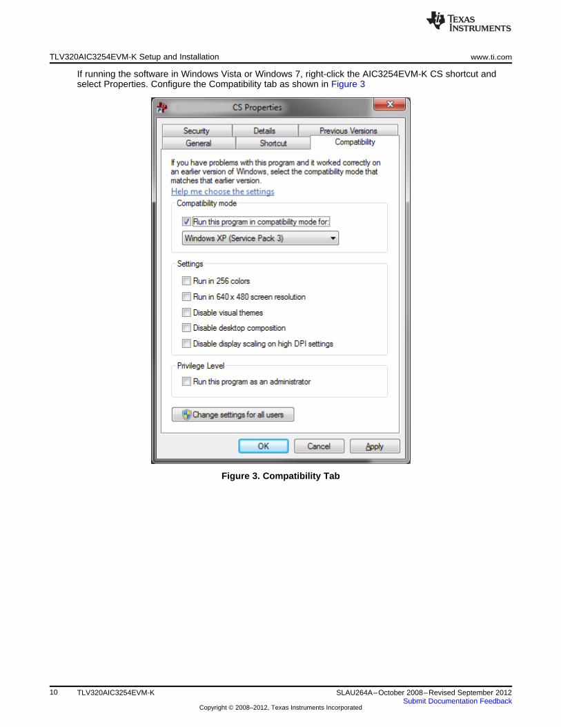
If running the software in Windows Vista or Windows 7, right-click the AIC3254EVM-K CS shortcut andselect Properties. Configure the Compatibility tab as shown in Figure 3
Figure 3. Compatibility Tab
10 TLV320AIC3254EVM-K SLAU264A–October 2008–Revised September 2012Submit Documentation Feedback
Copyright © 2008–2012, Texas Instruments Incorporated

www.ti.com AIC3254 Control Software
4 AIC3254 Control Software
The AIC3254 Control Software (CS) is an intuitive, easy-to-use, powerful tool to learn, evaluate, andcontrol the TLV320AIC3254. This tool was specifically designed to make learning the TLV320AIC3254software easy. The following sections describe the operation of this software.
NOTE: For configuration of the codec, the TLV320AIC3254 block diagram located in theTLV320AIC3254 data sheet is a good reference to help determine the signal routing.
4.1 Main Panel Window
The Main Panel window, shown in Figure 2, provides easy access to all the features of the AIC3254 CS.The Firmware Name and Version boxes provide information about the firmware loaded into the EVM'sEEPROM.
The USB-MODEVM Interface drop-down menu allows the user to select which communication protocolthe TAS1020B USB Controller uses to communicate with the TLV320AIC3254 or to toggle the TAS1020BGPIO pins. The TLV320AIC3254 supports I2C Standard, I2C Fast, and 8-bit register SPI. The USB-MODEVM Interface selection is global to all panels, including the Command-Line Interface. Tocommunicate to the TLV320AIC3254 using SPI, SW1 must be switched towards SPI and W14 must beset to 1-2 on the TLV320AIC3254EVM.
The Panel Selection Tree provides access to typical configurations, features, and other panels that allowthe user to control the TLV320AIC3254. The tree is divided into several categories which contain itemsthat pop up panels. A panel can be opened by double-clicking any item inside a category in the PanelSelection Tree.
Below the Panel Selection Tree are three buttons that pop up the following:
• Status Flags - Allows the user to monitor the TLV320AIC3254 status flags.
• Register Tables - A tool to monitor register pages.
• Command-Line Interface - A tool to execute/generate scripts and monitor register activity.
The USB LED indicates if the EVM kit is recognized by the software and the ACTIVITY LED illuminatesevery time a command request is sent.
The dialog box at the bottom of the Main Panel provides feedback of the current status of the software.
11SLAU264A–October 2008–Revised September 2012 TLV320AIC3254EVM-KSubmit Documentation Feedback
Copyright © 2008–2012, Texas Instruments Incorporated
AIC3254 Control Software www.ti.com
4.1.1 Typical Configurations
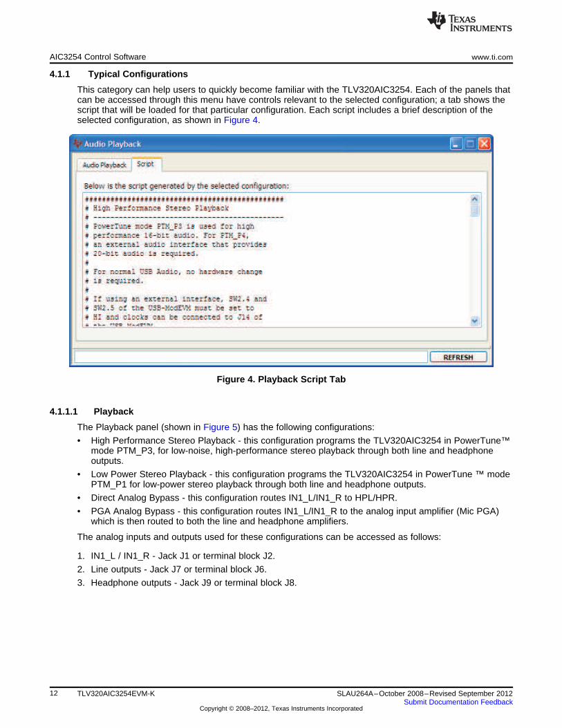
This category can help users to quickly become familiar with the TLV320AIC3254. Each of the panels thatcan be accessed through this menu have controls relevant to the selected configuration; a tab shows thescript that will be loaded for that particular configuration. Each script includes a brief description of theselected configuration, as shown in Figure 4.
Figure 4. Playback Script Tab
4.1.1.1 Playback
The Playback panel (shown in Figure 5) has the following configurations:
• High Performance Stereo Playback - this configuration programs the TLV320AIC3254 in PowerTune™mode PTM_P3, for low-noise, high-performance stereo playback through both line and headphoneoutputs.
• Low Power Stereo Playback - this configuration programs the TLV320AIC3254 in PowerTune ™ modePTM_P1 for low-power stereo playback through both line and headphone outputs.
• Direct Analog Bypass - this configuration routes IN1_L/IN1_R to HPL/HPR.
• PGA Analog Bypass - this configuration routes IN1_L/IN1_R to the analog input amplifier (Mic PGA)which is then routed to both the line and headphone amplifiers.
The analog inputs and outputs used for these configurations can be accessed as follows:
1. IN1_L / IN1_R - Jack J1 or terminal block J2.
2. Line outputs - Jack J7 or terminal block J6.
3. Headphone outputs - Jack J9 or terminal block J8.
12 TLV320AIC3254EVM-K SLAU264A–October 2008–Revised September 2012Submit Documentation Feedback
Copyright © 2008–2012, Texas Instruments Incorporated

www.ti.com AIC3254 Control Software
Figure 5. Playback Panel
4.1.1.2 Recording
The Recording panel (shown in Figure 6) has the following configurations:
• High Performance Stereo Recording - this configuration programs the TLV320AIC3254 in PowerTune™ mode PTM_R4, for low-noise, high-performance stereo recording. IN1_L and IN1_R are routed in asingle ended fashion.
• Low Power Stereo Recording - this configuration programs the TLV320AIC3254 in PowerTune ™mode PTM_R1 for low-power stereo playback. IN1_L and IN1_R are routed in a single ended fashion.
• Differential On-Board Microphone - this configuration programs the TLV320AIC3254's IN3_L andIN3_R as a differential pair. Jumpers related to the onboard microphone (W1 to W8) must be set totheir default configuration as described in Table 2.The analog inputs used for these configurations can be accessed as follows:
1. IN1_L / IN1_R - Jack J1 or terminal block J2.
2. IN3_L / IN3_R - Terminal block J4. Note that the onboard jack J5 must not be used for a differentialconfiguration.
13SLAU264A–October 2008–Revised September 2012 TLV320AIC3254EVM-KSubmit Documentation Feedback
Copyright © 2008–2012, Texas Instruments Incorporated

AIC3254 Control Software www.ti.com
Figure 6. Recording Panel
4.1.2 Features
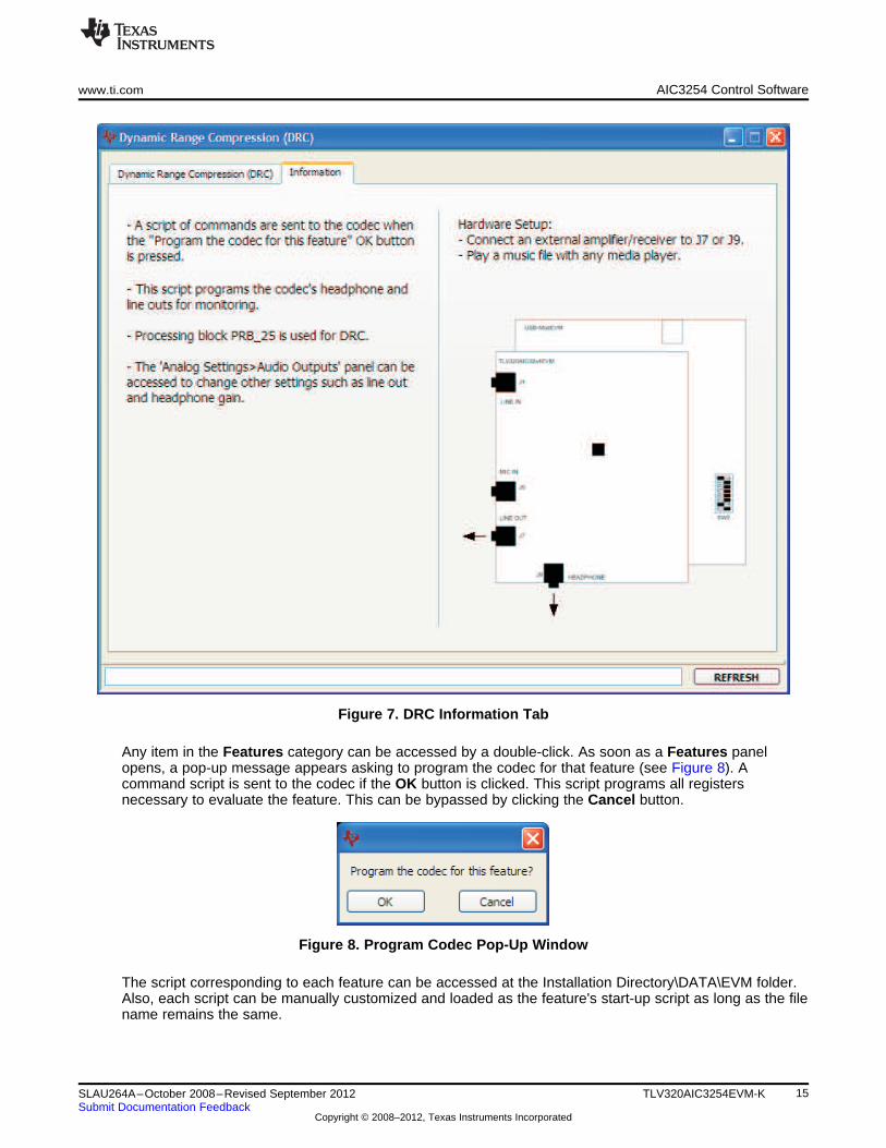
The Features category allows the user to evaluate various features of the TLV320AIC3254. Each of theFeatures panels include an Information tab that explains the feature and provides hardware setupinformation for easy evaluation, as seen in Figure 7.
14 TLV320AIC3254EVM-K SLAU264A–October 2008–Revised September 2012Submit Documentation Feedback
Copyright © 2008–2012, Texas Instruments Incorporated
www.ti.com AIC3254 Control Software
Figure 7. DRC Information Tab
Any item in the Features category can be accessed by a double-click. As soon as a Features panelopens, a pop-up message appears asking to program the codec for that feature (see Figure 8). Acommand script is sent to the codec if the OK button is clicked. This script programs all registersnecessary to evaluate the feature. This can be bypassed by clicking the Cancel button.
Figure 8. Program Codec Pop-Up Window
The script corresponding to each feature can be accessed at the Installation Directory\DATA\EVM folder.Also, each script can be manually customized and loaded as the feature's start-up script as long as the filename remains the same.
15SLAU264A–October 2008–Revised September 2012 TLV320AIC3254EVM-KSubmit Documentation Feedback
Copyright © 2008–2012, Texas Instruments Incorporated

AIC3254 Control Software www.ti.com
4.1.2.1 Adaptive Filtering
The TLV320AIC3254 features double-buffered filter coefficients which allow real-time filtering. TheTLV320AIC3254 features up to six cascaded biquads and a first-order IIR filter per DAC channel invarious signal processing blocks. Note that the TLV320AIC3254 has the potential for a larger amount ofbiquad sections if the embedded miniDSP is used for signal processing (see Section 4.1.3.1).
The Parametric Equalizer tab (shown in Figure 9) allows the user to modify the frequency response of thedigital input signal that is fed afterwards into the DAC channels. This application can be useful to fine-tunethe audio frequency response for a particular small speaker and enclosure system combination. Theprocessing block PRB_P2 (which is used for this application) has one IIR filter and six biquads in cascadeper audio channel. The first biquad (BQ0) is configured as a gain control which provides headroom andcompensation gain to the subsequent biquads in the cascade. Biquads BQ1 to BQ5 are configured for EQand/or shelf filters.
The Gain Q (quality) and fc (center frequency) parameters are available for the EQ filters whereas Gainfc (corner frequency) and Shelf Response are available for the shelf filters. These parameters can bemodified using their corresponding control. Also, by dragging a cursor in the frequency response window,the gain and fc for each biquad can be modified.
The PRB_P2 biquad coefficients are defined as 1.23, 2s complement format. Coefficients that are equal orlarger than unity must be normalized to comply with such format when converting from decimal format.This can be achieved by dividing all numerators of a biquad by a scale factor equal to the largestnumerator divided by 223 minus one (if the numerator is equal or larger than unity). Normalization results inan attenuated version of the same frequency response curve. The scale factor can then be used tocompensate for the attenuation at another unused biquad.
Figure 9. Adaptive Filtering Panel
16 TLV320AIC3254EVM-K SLAU264A–October 2008–Revised September 2012Submit Documentation Feedback
Copyright © 2008–2012, Texas Instruments Incorporated

www.ti.com AIC3254 Control Software
4.1.2.2 Automatic Gain Control
The left-channel Automatic Gain Control (AGC) can be enabled by checking the Enable Left AGC box(Figure 10). Pressing the Capture Audio button records the left-channel audio. Its corresponding data isdisplayed in the audio capture graph window. The small white window located at the bottom right of theAGC tab displays the audio waveform of the recorded data. Ensure that the AIC32x4 EVM is selected asthe computer's default audio capture device before pressing this button. To set the TLV320AIC3254EVM-K as the default audio device, open the Windows™ Control Panel → Sounds and Audio DevicesProperties and set the AIC32x4 EVM as the default audio recording device. Also, do not use any othermedia player or audio recording software while the control software is recording.
The target level and noise threshold parameters can be modified by dragging the horizontal cursor lineslocated at the audio capture graph window. Its numeric values are displayed to the right of the graph.Noise threshold can be disabled by unchecking the Enable Noise Threshold box. The AGC Max Gaincontrol sets the maximum allowed AGC PGA Gain. The AGC Gain indicator bar continuously displays thecontents of Page 0/Register 93 if the Enable Polling box is checked.
Other parameters can be accessed by checking the Advanced? box. For more information about AGC,see the Information tab and the data sheet.
Other flags related to this feature can be accessed at the Status Flags panel.
Figure 10. Automatic Gain Control Panel
17SLAU264A–October 2008–Revised September 2012 TLV320AIC3254EVM-KSubmit Documentation Feedback
Copyright © 2008–2012, Texas Instruments Incorporated

AIC3254 Control Software www.ti.com
4.1.2.3 Dynamic Range Compression
Dynamic Range Compression (DRC) can be enabled by checking the Enable Left DRC and EnableRight DRC boxes.
The level transfer characteristic graph is a function of the applied digital gain and the threshold parameter.The graph line is separated into two piece-wise linear regions where the red line represents the levelrange in which the DRC attenuation takes place, and the green line represents the level range in whichthe signal is not affected by DRC. As an example, setting the threshold to -24 dB with a gain to 24 dBimplies that an input signal strength variation from -48 dB (threshold - gain) to 0 dB results in an outputsignal strength variation from -24 dB to 0 dB, or a compression ratio of 2:1. Similarly, a threshold of -3 dBwith a gain of 24 dB implies that an input signal strength variation from -27 dB to 0 dB results in an outputsignal strength variation from -3 dB to 0 dB, or a ratio of 9:1. Note that a gain less than 0 dB does notresult in expansion.
The Attack and Decay are time domain parameters that control the rate in which the applied gain reachesthe target gain after the threshold level is crossed. As an example, a fast attack rate quickly reaches thetarget gain once the output signal crosses the programmed threshold region.
Other flags related to this feature can be accessed at the Status Flags panel.
Figure 11. Dynamic Range Compression Panel
18 TLV320AIC3254EVM-K SLAU264A–October 2008–Revised September 2012Submit Documentation Feedback
Copyright © 2008–2012, Texas Instruments Incorporated

www.ti.com AIC3254 Control Software
4.1.2.4 Headset Detection
The TLV320AIC3254EVM provides two terminal blocks (J8 and J4) that can be used to connect differenttypes of cellular headset jacks. For proper headset detection, the jack connections must comply with thefigure shown in the Headset Detection section of the datasheet.
The Headset Detection panel provides hardware setup information for a four-conductor stereo + cellularjack, as seen in Figure 12.
As an example, if stereo headphones are connected to the four-conductor jack, the tip and ring carry theAC-coupled HPL and HPR signal to the headphone speakers whereas the shield shorts the SCLK/MFP3pin to ground. This results in a stereo headset detection.
Checking the Enable Polling box displays the headset type at the Headset Type Detected box.
Other flags related to this feature can be accessed at the Status Flags panel.
Figure 12. Headset Detection Panel
4.1.2.5 DC Measurement
Terminal block J3 on the TLV320AIC3254EVM can be used to evaluate the DC measurement feature.The Information tab provides the hardware setup information.
The Left ADC (V) and Right ADC (V) boxes convert the register data to voltage. The voltage is derivedfrom the References shown at the upper right corner of the DC Measurement tab. The DC measurementregister data is in 2.22, 2s complement format.
19SLAU264A–October 2008–Revised September 2012 TLV320AIC3254EVM-KSubmit Documentation Feedback
Copyright © 2008–2012, Texas Instruments Incorporated

AIC3254 Control Software www.ti.com
Checking the Enable Polling box displays the DC measurement data.
Other flags related to this feature can be accessed at the Status Flags panel.
Figure 13. DC Measurement Panel
4.1.3 miniDSP Applications
The TLV320AIC3254 features two miniDSP cores, one for the ADC and another for the DAC.
Currently, the AIC3254 CS has two DAC miniDSP applications: Equalizers and Spectrum Analyzer. Visitthe TLV320AIC3254EVM-K product folder for updates and availability on new miniDSP applications.
See the miniDSP section in the data sheet (SLAS549) for information on how to develop custom miniDSPalgorithms.
4.1.3.1 Equalizers
The Equalizers miniDSP application features 20 cascaded biquad filters per DAC channel (Figure 14).Each of the 40 20-Band EQ sliders modify its corresponding biquad filter in the cascade as a function ofgain. Each Master slider controls the digital volume control of the TLV320AIC3254. All sliders can be setto track the opposing channel slider movement by turning on the Lock L+R switch. Preset configurationsare available at the red selection box below the graphic equalizer. A frequency slider movement changesany preset to Custom.
20 TLV320AIC3254EVM-K SLAU264A–October 2008–Revised September 2012Submit Documentation Feedback
Copyright © 2008–2012, Texas Instruments Incorporated

www.ti.com AIC3254 Control Software
The Small Speaker EQ section, contains filter presets that are suitable for small speaker applications.Emphasizing certain frequencies and reducing low-frequency energy provides higher volume with lessdistortion and more intelligible speech and music for small speakers. These presets use the first sevenbiquads of the cascade for filtering whereas the rest of the 13 graphic equalizer sliders can be used toemphasize other frequencies. This feature is enabled by setting the green ON/OFF switch to ON.
Although an option is available to program the codec for this feature when the panel pops up, provision ismade to re-program this miniDSP application by clicking the Program EQ into miniDSP button.
Figure 14. Equalizers miniDSP Application
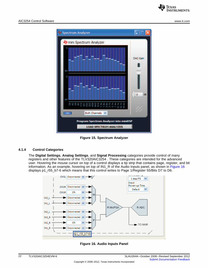
4.1.3.2 Spectrum Analyzer
The 20-Band Spectrum Analyzer provides a visual representation of the frequency content of the inputsignal (Figure 150. If Both Channels is selected in the selection box below the display window, theAIC3254 CS polls the registers related to both channels. To enable polling, set the ON/OFF switch to ON.
Modifying the DAC volume control does not affect the spectrum reading because the analysis is donebefore the DAC volume control.
Although an option is available to program the codec for this feature when the panel pops up, provision ismade to re-program this miniDSP application by clicking the Program Spectrum Analyzer into miniDSPbutton.
21SLAU264A–October 2008–Revised September 2012 TLV320AIC3254EVM-KSubmit Documentation Feedback
Copyright © 2008–2012, Texas Instruments Incorporated
AIC3254 Control Software www.ti.com
Figure 15. Spectrum Analyzer
4.1.4 Control Categories
The Digital Settings, Analog Settings, and Signal Processing categories provide control of manyregisters and other features of the TLV320AIC3254 . These categories are intended for the advanceduser. Hovering the mouse cursor on top of a control displays a tip strip that contains page, register, and bitinformation. As an example, hovering on top of IN1_R of the Audio Inputs panel, as shown in Figure 16displays p1_r55_b7-6 which means that this control writes to Page 1/Register 55/Bits D7 to D6.
Figure 16. Audio Inputs Panel
22 TLV320AIC3254EVM-K SLAU264A–October 2008–Revised September 2012Submit Documentation Feedback
Copyright © 2008–2012, Texas Instruments Incorporated

www.ti.com AIC3254 Control Software
Before changing a control, see the data sheet to ensure that a particular control is compatible with thecurrent state of the codec. As an example, some controls in the Analog Setup panel must be modified ina particular order as described in the data sheet. Other controls must only be modified with a specifichardware setup, such as powering up the AVDD LDO.
All controls update their status with respect to the register contents in the following conditions:
• A panel is opened.
• The Execute Command Buffer button in the Command-Line Interface is pressed.
• The Refresh button at the bottom right of a panel is pressed.
4.2 Status Flags Panel
The TLV320AIC3254 status flags can monitored in the Status Flags panel (Figure 17) which is locatedbelow the Panel Selection Tree . Pressing the POLL button continuously reads all the registers relevantto each flag and updates those flags accordingly. The rate at which the registers are read can be modifiedby changing the value in the Polling Interval numeric control. Note that a smaller interval reducesresponsiveness of other controls, especially volume sliders, due to bandwidth limitations. By default, thepolling interval is 200 ms and can be set to a minimum of 20 ms.
The Sticky Flags tab contains indicators whose corresponding register contents clear every time a read isperformed to that register. To read all the sticky flags, click the Read Sticky Flags button.
Figure 17. Status Flags Panel
4.3 Register Tables Panel
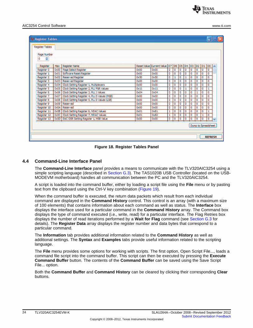
The contents of configuration and coefficient pages of the TLV320AIC3254 can be accessed through theRegister Tables panel (Figure 18).
The Page Number control changes to the page to be displayed in the register table. The register tablecontains page information such as the register name, reset value, current value, and a bitmap of thecurrent value. The contents of the selected page can be exported into a spreadsheet by clicking the Dumpto Spreadsheet button.
23SLAU264A–October 2008–Revised September 2012 TLV320AIC3254EVM-KSubmit Documentation Feedback
Copyright © 2008–2012, Texas Instruments Incorporated
AIC3254 Control Software www.ti.com
Figure 18. Register Tables Panel
4.4 Command-Line Interface Panel
The Command-Line Interface panel provides a means to communicate with the TLV320AIC3254 using asimple scripting language (described in Section G.3). The TAS1020B USB Controller (located on the USB-MODEVM motherboard) handles all communication between the PC and the TLV320AIC3254.
A script is loaded into the command buffer, either by loading a script file using the File menu or by pastingtext from the clipboard using the Ctrl-V key combination (Figure 19).
When the command buffer is executed, the return data packets which result from each individualcommand are displayed in the Command History control. This control is an array (with a maximum sizeof 100 elements) that contains information about each command as well as status. The Interface boxdisplays the interface used for a particular command in the Command History array. The Command boxdisplays the type of command executed (i.e., write, read) for a particular interface. The Flag Retries boxdisplays the number of read iterations performed by a Wait for Flag command (see Section G.3 fordetails). The Register Data array displays the register number and data bytes that correspond to aparticular command.
The Information tab provides additional information related to the Command History as well asadditional settings. The Syntax and Examples tabs provide useful information related to the scriptinglanguage.
The File menu provides some options for working with scripts. The first option, Open Script File..., loads acommand file script into the command buffer. This script can then be executed by pressing the ExecuteCommand Buffer button. The contents of the Command Buffer can be saved using the Save ScriptFile... option.
Both the Command Buffer and Command History can be cleared by clicking their corresponding Clearbuttons.
24 TLV320AIC3254EVM-K SLAU264A–October 2008–Revised September 2012Submit Documentation Feedback
Copyright © 2008–2012, Texas Instruments Incorporated

www.ti.com AIC3254 Control Software
Figure 19. Command-line Interface Panel
25SLAU264A–October 2008–Revised September 2012 TLV320AIC3254EVM-KSubmit Documentation Feedback
Copyright © 2008–2012, Texas Instruments Incorporated
www.ti.com
Appendix A EVM Connector Descriptions
This appendix contains the connection details for each of the main connectors on the EVM.
A.1 Analog Interface Connectors
A.1.1 Analog Dual-Row Socket Details, J11 and J21
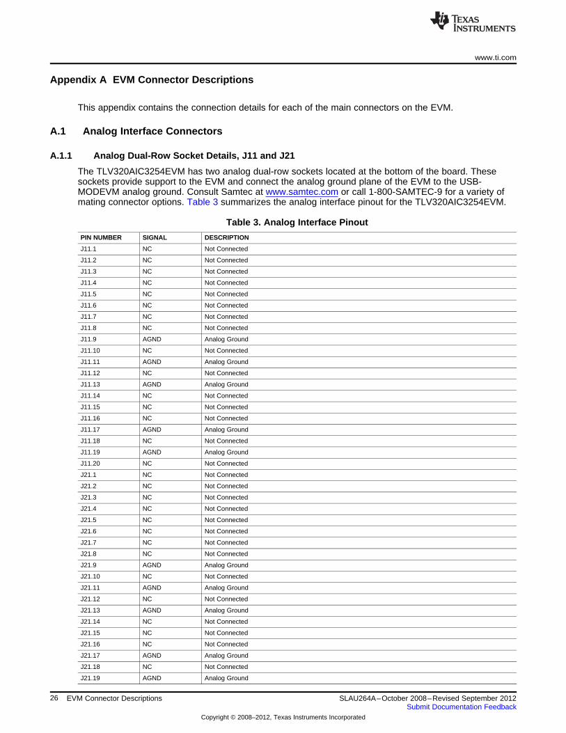
The TLV320AIC3254EVM has two analog dual-row sockets located at the bottom of the board. Thesesockets provide support to the EVM and connect the analog ground plane of the EVM to the USB-MODEVM analog ground. Consult Samtec at www.samtec.com or call 1-800-SAMTEC-9 for a variety ofmating connector options. Table 3 summarizes the analog interface pinout for the TLV320AIC3254EVM.
Table 3. Analog Interface Pinout
PIN NUMBER SIGNAL DESCRIPTION
J11.1 NC Not Connected
J11.2 NC Not Connected
J11.3 NC Not Connected
J11.4 NC Not Connected
J11.5 NC Not Connected
J11.6 NC Not Connected
J11.7 NC Not Connected
J11.8 NC Not Connected
J11.9 AGND Analog Ground
J11.10 NC Not Connected
J11.11 AGND Analog Ground
J11.12 NC Not Connected
J11.13 AGND Analog Ground
J11.14 NC Not Connected
J11.15 NC Not Connected
J11.16 NC Not Connected
J11.17 AGND Analog Ground
J11.18 NC Not Connected
J11.19 AGND Analog Ground
J11.20 NC Not Connected
J21.1 NC Not Connected
J21.2 NC Not Connected
J21.3 NC Not Connected
J21.4 NC Not Connected
J21.5 NC Not Connected
J21.6 NC Not Connected
J21.7 NC Not Connected
J21.8 NC Not Connected
J21.9 AGND Analog Ground
J21.10 NC Not Connected
J21.11 AGND Analog Ground
J21.12 NC Not Connected
J21.13 AGND Analog Ground
J21.14 NC Not Connected
J21.15 NC Not Connected
J21.16 NC Not Connected
J21.17 AGND Analog Ground
J21.18 NC Not Connected
J21.19 AGND Analog Ground
26 EVM Connector Descriptions SLAU264A–October 2008–Revised September 2012Submit Documentation Feedback
Copyright © 2008–2012, Texas Instruments Incorporated
www.ti.com Analog Interface Connectors
Table 3. Analog Interface Pinout (continued)
PIN NUMBER SIGNAL DESCRIPTION
J21.20 NC Not Connected
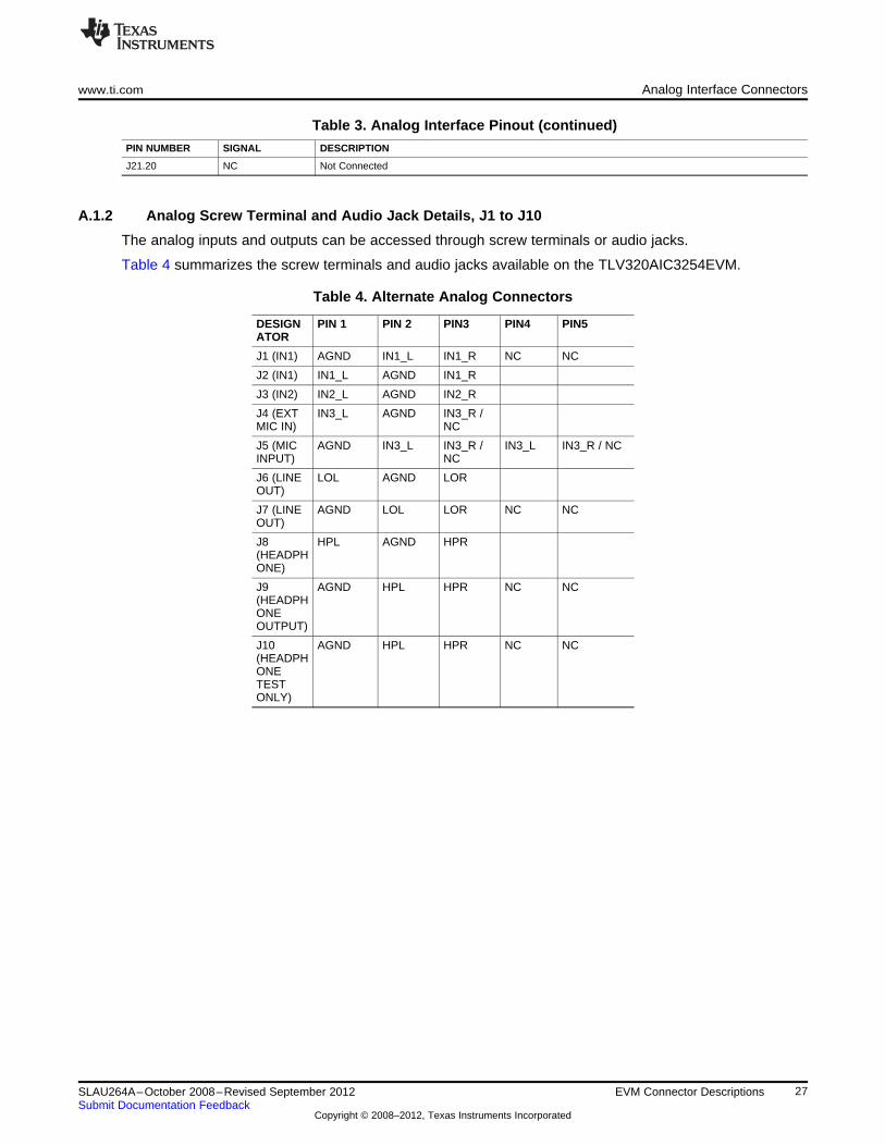
A.1.2 Analog Screw Terminal and Audio Jack Details, J1 to J10
The analog inputs and outputs can be accessed through screw terminals or audio jacks.
Table 4 summarizes the screw terminals and audio jacks available on the TLV320AIC3254EVM.
Table 4. Alternate Analog Connectors
DESIGN PIN 1 PIN 2 PIN3 PIN4 PIN5ATOR
J1 (IN1) AGND IN1_L IN1_R NC NC
J2 (IN1) IN1_L AGND IN1_R
J3 (IN2) IN2_L AGND IN2_R
J4 (EXT IN3_L AGND IN3_R /MIC IN) NC
J5 (MIC AGND IN3_L IN3_R / IN3_L IN3_R / NCINPUT) NC
J6 (LINE LOL AGND LOROUT)
J7 (LINE AGND LOL LOR NC NCOUT)
J8 HPL AGND HPR(HEADPHONE)
J9 AGND HPL HPR NC NC(HEADPHONEOUTPUT)
J10 AGND HPL HPR NC NC(HEADPHONETESTONLY)
27SLAU264A–October 2008–Revised September 2012 EVM Connector DescriptionsSubmit Documentation Feedback
Copyright © 2008–2012, Texas Instruments Incorporated

Digital Interface Connectors, P12/J12 and P22/J22 www.ti.com
A.2 Digital Interface Connectors, P12/J12 and P22/J22
The TLV320AIC3254EVM is designed to easily interface with multiple control platforms. Samtec partnumbers SSW-110-22-F-D-VS-K and TSM-110-01-T-DV-P provide a convenient 10-pin, dual-rowheader/socket combination at P12/J12 and P22/J22. These headers/sockets provide access to the digitalcontrol and serial data pins of the device. Consult Samtec at www.samtec.com or call 1-800- SAMTEC-9for a variety of mating connector options. Table 5 summarizes the digital interface pinout for theTLV320AIC3254EVM.
Table 5. Digital Interface Pinout
PIN NUMBER SIGNAL DESCRIPTION
P12.1/J12.1 NC Not Connected
P12.2/J12.2 NC Not Connected
P12.3/J12.3 SCLK SPI Serial Clock
P12.4/J12.4 DGND Digital Ground
P12.5/J12.5 NC Not Connected
P12.6/J12.6 NC Not Connected
P12.7/J12.7 /SS SPI Chip Select
P12.8/J12.8 NC Not Connected
P12.9/J12.9 NC Not Connected
P12.10/J12.10 DGND Digital Ground
P12.11/J12.11 MOSI SPI MOSI Slave Serial Data Input
P12.12/J12.12 NC Not Connected
P12.13/J12.13 MISO SPI MISO Slave Serial Data Output
P12.14/J12.14 RESET TAS1020B Reset
P12.15/J12.15 NC Not Connected
P12.16/J12.16 SCL I2C Serial Clock
P12.17/J12.17 NC Not Connected
P12.18/J12.18 DGND Digital Ground
P12.19/J12.19 NC Not Connected
P12.20/J12.20 SDA I2C Serial Data Input/Output
P22.1/J22.1 NC Not Connected
P22.2/J22.2 NC Not Connected
P22.3/J22.3 BCLK Audio Serial Data Bus Bit Clock (Input/Output)
P22.4/J22.4 DGND Digital Ground
P22.5/J22.5 NC Not Connected
P22.6/J22.6 NC Not Connected
P22.7/J22.7 WCLK Audio Serial Data Bus Word Clock (Input/Output)
P22.8/J22.8 NC Not Connected
P22.9/J22.9 NC Not Connected
P22.10/J22.10 DGND Digital Ground
P22.11/J22.11 DIN Audio Serial Data Bus Data Input (Input)
P22.12/J22.12 NC Not Connected
P22.13/J22.13 DOUT Audio Serial Data Bus Data Output (Output)
P22.14/J22.14 NC Not Connected
P22.15/J22.15 NC Not Connected
P22.16/J22.16 NC Not Connected
P22.17/J22.17 MCLK Master Clock Input
P22.18/J22.18 DGND Digital Ground
P22.19/J22.19 NC Not Connected
P22.20/J22.20 NC Not Connected
28 EVM Connector Descriptions SLAU264A–October 2008–Revised September 2012Submit Documentation Feedback
Copyright © 2008–2012, Texas Instruments Incorporated
www.ti.com Power Supply Connector Pin Header, P23/J23
Note that P22/J22 comprises the signals needed for an I2S™ serial digital audio interface; the controlinterface ( I2C™ and RESET) signals are routed to P12/J12.
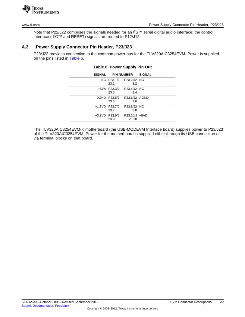
A.3 Power Supply Connector Pin Header, P23/J23
P23/J23 provides connection to the common power bus for the TLV320AIC3254EVM. Power is suppliedon the pins listed in Table 6.
Table 6. Power Supply Pin Out
SIGNAL PIN NUMBER SIGNAL
NC P23.1/J P23.2/J2 NC23.1 3.2
+5VA P23.3/J P23.4/J2 NC23.3 3.4
DGND P23.5/J P23.6/J2 AGND23.5 3.6
+1.8VD P23.7/J P23.8/J2 NC23.7 3.8
+3.3VD P23.9/J P23.10/J +5VD23.9 23.10
The TLV320AIC3254EVM-K motherboard (the USB-MODEVM Interface board) supplies power to P23/J23of the TLV320AIC3254EVM. Power for the motherboard is supplied either through its USB connection orvia terminal blocks on that board.
29SLAU264A–October 2008–Revised September 2012 EVM Connector DescriptionsSubmit Documentation Feedback
Copyright © 2008–2012, Texas Instruments Incorporated

www.ti.com
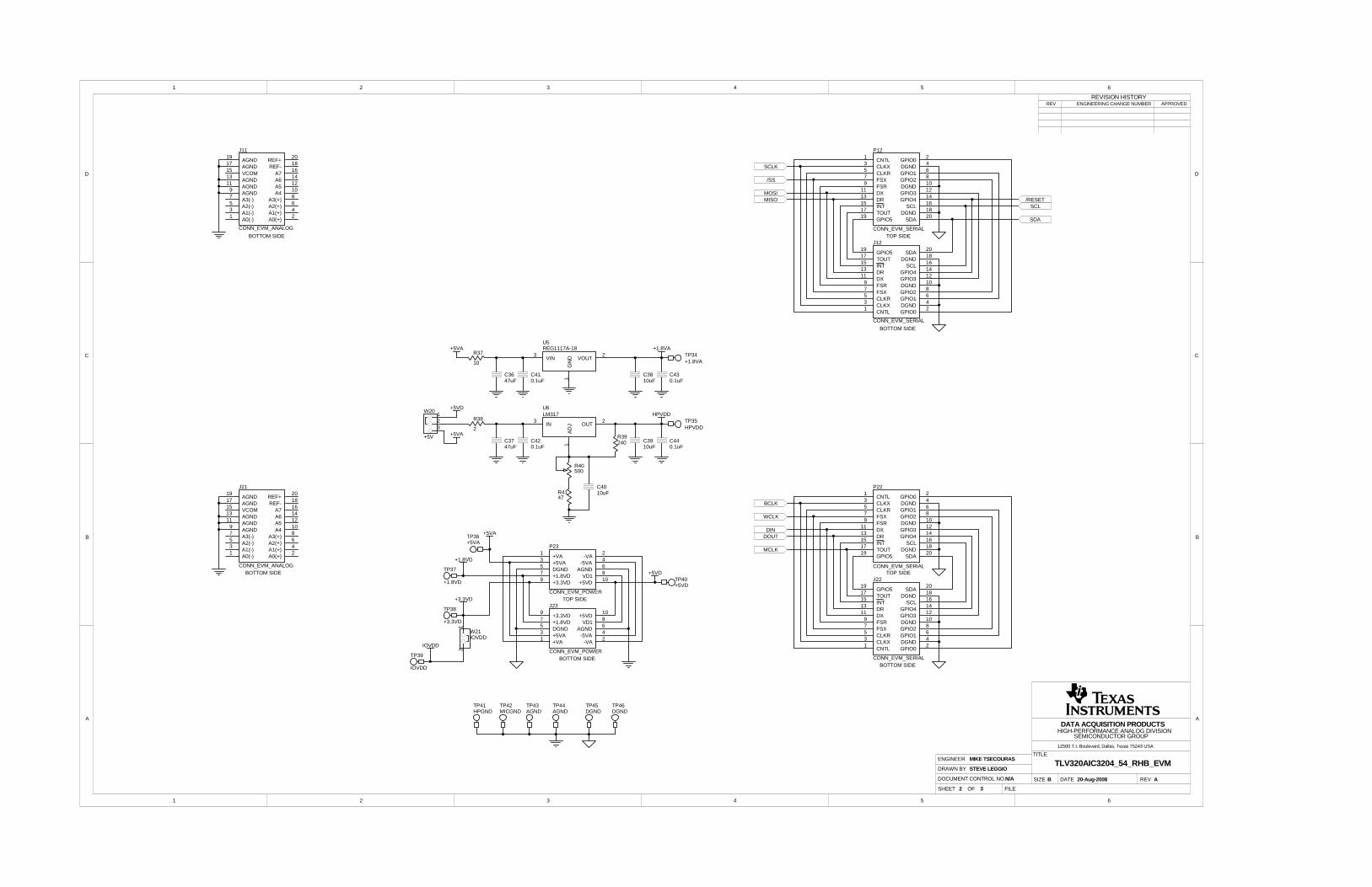
Appendix B TLV320AIC3254EVM Schematic
The schematic diagram for the TLV320AIC3254EVM is provided as a reference.
30 TLV320AIC3254EVM Schematic SLAU264A–October 2008–Revised September 2012Submit Documentation Feedback
Copyright © 2008–2012, Texas Instruments Incorporated

1 2 3 4 5 6
A
B
C
D
654321
D
C
B
A
Revision HistoryREV ECN Number Approved
ti12500 T.I. Boulevard, Dallas, Texas 75243 USA
TITLE
SHEET OF FILE
SIZE DATE REV20-Aug-2008
DRAWN BY
ENGINEER
A
DATA ACQUISITION PRODUCTSHIGH PERFORMANCE ANALOG DIVISION
SEMICONDUCTOR GROUP
Steve Leggio
Mike Tsecouras
A
1 3
TLV320AIC3204_54_RHB_EVM
DOCUMENT CONTROL NO.N/A
SINGLE-ENDEDSINGLE-ENDEDMONOMONO
INOUT
1-2
SINGLE-ENDED
IN
INOUT
IN3_L IN3_LIN3_RIN3_L
JUMPERSETTINGS
MICROPHONE CONFIGURATION
DIFFERENTIAL
OUT
IN2-3
IN3_LIN3_R
W4
W7W8
SINGLE-ENDEDSINGLE-ENDEDMONOMONO
OUTOUT
INOUTOUT1-2
SINGLE-ENDED
IN3_L IN3_LIN3_R
IN3_L
INPUT CONFIGURATION
DIFFERENTIAL
OUT
INOUT
IN3_LIN3_R
CODECINPUTS IN3_R
OUT
INOUT
MODE
Ring is connected to IN3_R.
Stereo electret microphones. Bias provided to both inputs. Ring is connected to IN3_R.
IN3_R is AC-coupled to AVSS.
Differential electret microphone. IN3_L & IN3_R configured as differential pair.
Microphone bias provided on tip. IN3_R AC coupled to GND. Ring not connected to circuit.
Ring is connected to IN3_R.
Microphone bias provided on tip. IN3_R AC coupled to GND. Ring not connected to circuit.
Differential line in. IN3_L & IN3_R configured as differential pair.
DIFFERENTIALSINGLE-ENDED
ININ2-31-2
IN3_L IN3_L
MICROPHONE CONFIGURATION
Differential - Mono.
Single Ended - Mono.
ONBOARD ELECTRETJACK LINEEXTERNAL ELECTRET
W2W3
OUTOUT
OUTOUT
OUTOUT
OUTOUT
OUTOUT
OUTOUT
OUTOUT
OUTOUT
ININ
ININ
MONO MONOSTEREO MONO STEREO MONO
ONBOARD MICJUMPERS
INPUT CONFIG W5W6
OUT
OUTOUTIN IN
INOUTOUT OUTOUTN/AN/A N/AN/A
OUTINOUT
OUTININ
Daughtercard_InterfaceDaughtercard_Interface.SCH
AIC3204_54_RHBAIC3204_54_RHB.SCH
IN3_R
INOUT
1-2
OUT
OUT
TYPICAL INPUT CONFIGURATIONS (IN3_L & IN3_R)
INPUT TYPE
DESCRIPTION
1 2 3 4 5 6
A
B
C
D
654321
D
C
B
Ati
12500 T.I. Boulevard, Dallas, Texas 75243 USA
SHEET
TITLE
DRAWN BY
OF FILE
ENGINEER
SIZE DATE REV
REVISION HISTORY
20-Aug-2008
REV ENGINEERING CHANGE NUMBER APPROVED
DATA ACQUISITION PRODUCTSHIGH-PERFORMANCE ANALOG DIVISION
ADOCUMENT CONTROL NO. B
+5VA
SEMICONDUCTOR GROUP
A0(+)2
A1(+)4
A2(+)6
A3(+)8
A410
A512
A614
A716
REF-18
REF+20
A0(-)1
A1(-)3
A2(-)5
A3(-)7
AGND9
AGND11
AGND13
VCOM15
AGND17
AGND19
J11
CONN_EVM_ANALOG
MIKE TSECOURAS
STEVE LEGGIO
2 3
TLV320AIC3204_54_RHB_EVM
N/A
A0(+)2
A1(+)4
A2(+)6
A3(+)8
A410
A512
A614
A716
REF-18
REF+20
A0(-)1
A1(-)3
A2(-)5
A3(-)7
AGND9
AGND11
AGND13
VCOM15
AGND17
AGND19
J21
CONN_EVM_ANALOG
-VA2
-5VA4
AGND6
VD18
+5VD10
+VA1
+5VA3
DGND5
+1.8VD7
+3.3VD9
J23
CONN_EVM_POWER
-VA2
-5VA4
AGND6
VD18
+5VD10
+VA1
+5VA3
DGND5
+1.8VD7
+3.3VD9
P23
CONN_EVM_POWER
GPIO02
DGND4
GPIO16
GPIO28
DGND10
GPIO312
GPIO414
SCL16
DGND18
SDA20
CNTL1
CLKX3
CLKR5
FSX7
FSR9
DX11
DR13
INT15
TOUT17
GPIO519
P12
CONN_EVM_SERIAL
GPIO02
DGND4
GPIO16
GPIO28
DGND10
GPIO312
GPIO414
SCL16
DGND18
SDA20
CNTL1
CLKX3
CLKR5
FSX7
FSR9
DX11
DR13
INT15
TOUT17
GPIO519
J12
CONN_EVM_SERIAL
GPIO02
DGND4
GPIO16
GPIO28
DGND10
GPIO312
GPIO414
SCL16
DGND18
SDA20
CNTL1
CLKX3
CLKR5
FSX7
FSR9
DX11
DR13
INT15
TOUT17
GPIO519
P22
CONN_EVM_SERIAL
GPIO02
DGND4
GPIO16
GPIO28
DGND10
GPIO312
GPIO414
SCL16
DGND18
SDA20
CNTL1
CLKX3
CLKR5
FSX7
FSR9
DX11
DR13
INT15
TOUT17
GPIO519
J22
CONN_EVM_SERIAL
/RESET
SDA
SCL
BOTTOM SIDE
BOTTOM SIDE
TOP SIDE
BOTTOM SIDE
TOP SIDE
BOTTOM SIDE
TOP SIDE
BOTTOM SIDE
+1.8VD
+3.3VD
TP41HPGND
TP44AGND
TP42MICGND
TP43AGND
C420.1uF
C3747uF
C4010uF
R39240
R4147
+5VA
TP36+5VA
TP35HPVDD
R40500
TP37
+1.8VD
TP38
+3.3VD
IOVDD
TP39
IOVDD
IN3
OUT2
AD
J1
U6LM317
C440.1uF
C3910uF
HPVDD
DOUT
BCLK
WCLK
DIN
MCLK
SCLK
MISOMOSI
/SS
R38
2
+1.8VA
C410.1uF
C3647uF
+5VAR37
10
C430.1uF
C3810uF
TP34+1.8VA
VIN3
VOUT2
GN
D1
U5REG1117A-18
+5VDTP40+5VD
+5VD123
W20
+5V
12
W21IOVDD
TP45DGND
TP46DGND

1 2 3 4 5 6
A
B
C
D
654321
D
C
B
A
Revision HistoryREV ECN Number Approved
ti12500 T.I. Boulevard, Dallas, Texas 75243 USA
TITLE
SHEET OF FILE
SIZE DATE REV20-Aug-2008
DRAWN BY
ENGINEER
A
DATA ACQUISITION PRODUCTSHIGH PERFORMANCE ANALOG DIVISION
SEMICONDUCTOR GROUP
Steve Leggio
Mike Tsecouras
A
1 3
TLV320AIC3204_54_RHB_EVM
DOCUMENT CONTROL NO.N/A
SC
L/S
SZ
SD
A/M
OS
I
DOUT
TP19DOUT
BCLK
WCLK
DIN
TP22BCLK
TP21WCLK
TP20DIN
MCLK
TP23MCLK
C30
0.1uFC35
22uF
12
W17
DV
DD
AV
DD
TP3IN2_L1
2
3
J3 IN2C3
0.47uF
C4
0.47uF
TP4IN2_R
TP1IN1_L1
2
3
J2 IN1C1
0.47uF
C2
0.47uF
TP2IN1_R
MIS
O
SP
I_S
EL
IN1_
L
IN1_
R
IN2_
L
HEADPHONE JACK
IOVDDC260.1uF
C3110uF 12
W16
SCLK
IN2_
R
LOR
LOL
IN3_R
IN3_L
MICBIAS
REF
MCLK
BCLK
WCLK
DIN
DOUT
SC
LK
/MIC
_DE
T
HP
R
HP
L GP
IO
/RE
SE
T
LD
O_S
EL
C21
47uFC22
47uFTP12HPR
TP11HPL
1
2
3
J8
HEADPHONE
C1947nF
12
W9
R9100
R2916 C20
47nF
12
W10
R10100
R3016
HPR
HPL
5
13
42J9
SJ1-3515-SMT
TP24GPIO
12W11
12W12
MISO
MOSI
/SS
R254.7K
IOVDD
HPVDD
C29
0.1uFC34
22uF
12
W18
C27
0.1uF
C32
10uF
TP14SDA
TP13SCL
SCL
SDA
+3.3VD
VCC8
VSS4
SDA5
SCL6
A01
A12
A23
WP7
U2
MICROCHIP_24LC64
R362.7K
R352.7K
12
W13
R342.7K
C23
0.1uF
+3.3VD
RED
C25
0.1uF
1A1
1B2
1Y7
VCC8
GND4
2Y3
2B6
2A5
U4 SN74LVC2G00
213
SW3
/RESET+3.3VD
R3310K
+3.3VD
R3210K
TP25/RESET
R31
332
C24
0.1uF
+3.3VDD1
/RESET
A1
B2
Y4
VCC5
GND3
U3
SN74LVC1G08
/RESETR28
4.7K
+3.3VD1 2
W15
"RESET"
SHOWN POSITION"/RESET"
C28
0.1uFC33
22uF
12
W19
+1.8VA
+1.8VD
IOVDD
R264.7K
TP16MOSI
TP17SCLK
TP15/SS
TP18MISO
C1747nF
C1847nF
R7
100
R8
100
C15
1.0uF
C16
1.0uF
LINE OUT
1
2
3
J6
LINE OUT
LOR
LOL
5
13
42
J7SJ1-3515-SMT
TP9LOL
TP10LOR
TP33LDO_SEL
TP30AVDD
54
23
6
1
879
111012
SW2
4PDT_ESW_EG4208
54
23
6
1
879
111012
SW14PDT_ESW_EG4208
MCLK1
BCLK2
WCLK3
DIN4
DOUT5
IOVDD6
IOVSS7
SCLK/MIC_DET8
SC
L/S
S9
SD
A/M
OS
I10
MIS
O11
SP
ISE
LEC
T12
IN1_
L13
IN1_
R14
IN2_
L15
IN2_
R16
AVSS17
REF18
MICBIAS19
IN3_L20
IN3_R21
LOL22
LOR23
AVDD24
HP
VD
D26
HP
R27
DV
SS
28
DV
DD
29
LDO
_SE
LEC
T30
RE
SE
TZ
31
GP
IO32
HP
L25
PPAD0
U1
TLV320AIC3254
TP26VREF
IN1_L
IN1_R
IN2_L
IN2_R
TP31HPVDD
TP32DVDD
EXT MIC IN
5
13
42J1
SJ1-3515-SMT
R11
0
R12
0C14NI
C13NI
C12NI
SW1:I2C SEL = 0SPI SEL = 1
SW2:EXTERNAL AVDD & DVDD = 0INTERNAL AVDD & DVDD = 1
IOVDD
R274.7K
TP27SPI_SEL
TP29SDA/MOSI
TP28SCL/SSZ
123
W14SCLK/MIC_DET
MIC DET used only with I2C interface.
TP6IN3_L
R61.0K
C6
0.47uF
C547uF
R11.0K
C7
0.47uF
R51.0K
5
13
42J5
SJ1-3515-SMT
12
MK1
MD9745APZ-F
R2100K
1
2
3
J4
EXT MIC IN
ONBOARD MIC
12
W2
12
W3
TP7IN3_R
R4
1.2K
R32.2K
C10NI
C11NI
12
3W1
MIC BIAS SEL
1
2
3
W8
1 2W4
1 2W5
1 2W6
TP5MIC BIAS
R19
0R20
0R21
0R22
0
R13
0R14
0
R15
0R16
0
R17
0
R18
0
R24
0
R23
0
TEST ONLY
5
13
42J10
SJ1-3515-SMT
C10, and C11 are not installed, but can be used to filter noise.
HEADPHONE
1 2W23
1 2W22
TP8EXT.BIAS
1 2W7

www.ti.com
Appendix C TLV320AIC3254EVM Layout Views
C.1 Layout Views
Figure 20. Top Layer
Figure 21. Mid-Layer 1
31SLAU264A–October 2008–Revised September 2012 TLV320AIC3254EVM Layout ViewsSubmit Documentation Feedback
Copyright © 2008–2012, Texas Instruments Incorporated

Layout Views www.ti.com
Figure 22. Mid-Layer 2
Figure 23. Bottom Layer
32 TLV320AIC3254EVM Layout Views SLAU264A–October 2008–Revised September 2012Submit Documentation Feedback
Copyright © 2008–2012, Texas Instruments Incorporated

www.ti.com Layout Views
Figure 24. Top Overlay
Figure 25. Bottom Overlay
33SLAU264A–October 2008–Revised September 2012 TLV320AIC3254EVM Layout ViewsSubmit Documentation Feedback
Copyright © 2008–2012, Texas Instruments Incorporated

Layout Views www.ti.com
Figure 26. Drill Drawing
Figure 27. Composite
34 TLV320AIC3254EVM Layout Views SLAU264A–October 2008–Revised September 2012Submit Documentation Feedback
Copyright © 2008–2012, Texas Instruments Incorporated
www.ti.com
Appendix D TLV320AIC3254EVM Bill of Materials
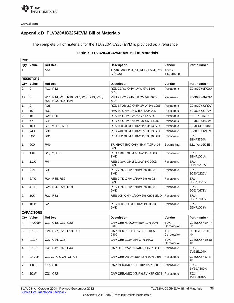
The complete bill of materials for the TLV320AIC3254EVM is provided as a reference.
Table 7. TLV320AIC3254EVM Bill of Materials
PCB
Qty Value Ref Des Description Vendor Part number
1 N/A TLV320AIC3204_54_RHB_EVM_Rev TexasA (PCB) Instruments
RESISTORS
Qty Value Ref Des Description Vendor Part number
2 0 R11, R12 RES ZERO OHM 1/4W 5% 1206 Panasonic EJ-8GEY0R00VS.D.
12 0 R13, R14, R15, R16, R17, R18, R19, R20, RES ZERO OHM 1/10W 5% 0603 Panasonic EJ-3GEY0R00VR21, R22, R23, R24 S.D.
1 2 R38 RESISTOR 2.0 OHM 1/4W 5% 1206 Panasonic EJ-8GEYJ2R0V
1 10 R37 RES 10 OHM 1/4W 5% 1206 S.D. Panasonic EJ-8GEYJ100V
2 16 R29, R30 RES 16 OHM 1W 5% 2512 S.D. Panasonic EJ-1TYJ160U
1 47 R41 RES 47 OHM 1/10W 5% 0603 S.D. Panasonic EJ-3GEYJ470V
4 100 R7, R8, R9, R10 RES 100 OHM 1/10W 1% 0603 S.D. Panasonic EJ-3EKF1000V
1 240 R39 RES 240 OHM 1/10W 5% 0603 S.D. Panasonic EJ-3GEYJ241V
1 332 R31 RES 332 OHM 1/10W 1% 0603 SMD Panasonic ERJ-3EKF3320V
1 500 R40 TRIMPOT 500 OHM 4MM TOP ADJ Bourns Inc. 3214W-1-501ESMD
3 1.0K R1, R5, R6 RES 1.00K OHM 1/10W 1% 0603 Panasonic ERJ-SMD 3EKF1001V
1 1.2K R4 RES 1.20K OHM 1/10W 1% 0603 Panasonic ERJ-SMD 3EKF1201V
1 2.2K R3 RES 2.2K OHM 1/10W 5% 0603 Panasonic ERJ-SMD 3GEYJ222V
3 2.7K R34, R35, R36 RES 2.7K OHM 1/10W 5% 0603 Panasonic ERJ-SMD 3GEYJ272V
4 4.7K R25, R26, R27, R28 RES 4.7K OHM 1/10W 5% 0603 Panasonic ERJ-SMD 3GEYJ472V
2 10K R32, R33 RES 10K OHM 1/10W 5% 0603 SMD Panasonic ERJ-3GEYJ103V
1 100K R2 RES 100K OHM 1/10W 1% 0603 Panasonic ERJ-SMD 3EKF1003V
CAPACITORS
Qty Value Ref Des Description Vendor Part number
4 47000pF C17, C18, C19, C20 CAP CER 47000PF 50V X7R 10% TDK C1608X7R1H470603 Corporation 3K
5 0.1uF C26, C27, C28, C29, C30 CAP CER .10UF 6.3V X5R 10% TDK C1005X5R0J100402 Corporation 4K
3 0.1uF C23, C24, C25 CAP CER .1UF 25V X7R 0603 TDK C1608X7R1E10Corporation 4K
4 0.1uF C41, C42, C43, C44 CAP .1UF 25V CERAMIC X7R 0805 Panasonic ECJ-2VB1E104K
6 0.47uF C1, C2, C3, C4, C6, C7 CAP CER .47UF 10V X5R 10% 0603 Panasonic C1608X5R1A474K
2 1.0uF C15, C16 CAP CERAMIC 1UF 10V X5R 0603 Panasonic ECJ-BVB1A105K
2 10uF C31, C32 CAP CERAMIC 10UF 6.3V X5R 0603 Panasonic ECJ-1VB0J106M
35SLAU264A–October 2008–Revised September 2012 TLV320AIC3254EVM Bill of MaterialsSubmit Documentation Feedback
Copyright © 2008–2012, Texas Instruments Incorporated

Appendix D www.ti.com
Table 7. TLV320AIC3254EVM Bill of Materials (continued)
3 10uF C38, C39, C40 CAP CERAMIC 10UF 10V X5R 0805 Panasonic ECJ-2FB1A106K
3 22uF C33, C34, C35 CAP CER 22UF 6.3V X5R 20% 0805 TDK C2012X5R0J22Corporation 6M
5 47uF C5, C21, C22, C36, C37 CAP CER 47UF 10V X5R 1210 Murata GRM32ER61A476KE20L
2 no value C10, C11 CAP 0603 N/A N/A- notinstalled
3 no value C12, C13, C14 CAP 1206 N/A N/A- notinstalled
INTEGRATED CIRCUITS
Qty Value Ref Des Description Vendor Part number
1 U1 Audio Codec Texas TLV320AIC3254Instruments IRHB
1 U2 IC SERIAL EEPROM 64K 2.5V 8- MicroChip 24LC64-I/SNSOIC
1 U3 Single 2-Input Positive-AND Gate Texas SN74LVC1G08Instruments DBVR
1 U4 Dual 2-Input Positive-NAND Gate Texas SN74LVC2G00Instruments DCTR
1 U5 Single Output LDO, 1.0A, Fixed(1.8V) Texas REG1117A-1.8Instruments
1 U6 3-Pin 1.5-A Adjustable Voltage Texas LM317DCYRegulator Instruments
MISCELLANEOUS ITEMS
Qty Value Ref Des Description Vendor Part number
1 D1 LED THIN 635NM RED DIFF 0805 Lumex SML-SMD LXT0805IW-TR
1 MK1 Omnidirectional Microphone Cartridge Knowles MD9745APZ-FAcoustics
or alternate Knowles MD9745APA-1Acoustics
2 SW1-SW2 SWITCH SLIDE 4PDT 30V RT E-Switch EG4208ANGLE
1 SW3 SWITCH SLIDE SPDT 30V.2A PC E-Switch EG1218MNT
5 J2, J3, J4, J6, J8 Screw Terminal Block, 3 Position On Shore ED555/3DSTechnology
5 J1, J5, J7, J9, J10 3.5mm Audio Jack, T-R-S, SMD CUI Inc. SJ1-3515-SMT
or alternate KobiConn 161-3335-E
11 not TP26, TP30, TP31, TP32, TP34, TP35, TP36, TEST POINT PC MINI .040"D RED Keystone 5000installed TP37, TP38, TP39, TP40 Electronics
29 not TP1, TP2, TP3, TP4, TP5, TP6, TP7, TP8, TEST POINT PC MINI .040"D WHITE Keystone 5002installed TP9, TP10, TP11, TP12, TP13, TP14, TP15, Electronics
TP16, TP17, TP18, TP19, TP20, TP21, TP22,TP23, TP24, TP25, TP27, TP28, TP29, TP33
6 TP41, TP42, TP43, TP44, TP45, TP46 TEST POINT PC MULTI PURPOSE Keystone 5011BLK Electronics
2 P12, P22 20 Pin SMT Plug Header Samtec TSM-110-01-L-DV-P
4 J11, J12, J21, J22 20 pin SMT Socket Header Samtec SSW-110-22-F-D-VS-K
1 P23 10 Pin SMT Plug Header Samtec TSM-105-01-L-DV-P
36 TLV320AIC3254EVM Bill of Materials SLAU264A–October 2008–Revised September 2012Submit Documentation Feedback
Copyright © 2008–2012, Texas Instruments Incorporated

www.ti.com Appendix D
Table 7. TLV320AIC3254EVM Bill of Materials (continued)
1 J23 10 pin SMT Socket Header Samtec SSW-105-22-F-D-VS-K
14 W2, W3, W4, W5, W6, W7, W9, W10, W11, 2 Pin Thru-hole Plug Header Samtec TSW-102-07-L-W12, W13, W15, W22, W23 (Jumper), 0 .1" spacing S
5 W16, W17, W18, W19, W21 Bus Wire (18-22 Gauge)
4 W1, W8, W14, W20 3 Position Jumper , 0 .1" spacing Samtec TSW-103-07-L-S
Installed Installed per test procedure. Header Shorting Block Samtec SNT-100-BK-Tper testprocedure.
ATTENTION: All components must be Rhos compliant. Some part numbers may be either leaded or Rhos. Verify that purchasedcomponents are Rhos compliant.
37SLAU264A–October 2008–Revised September 2012 TLV320AIC3254EVM Bill of MaterialsSubmit Documentation Feedback
Copyright © 2008–2012, Texas Instruments Incorporated

www.ti.com
Appendix E USB-MODEVM Schematic
The schematic diagram for USB-MODEVM Interface Board is provided as a reference.
38 USB-MODEVM Schematic SLAU264A–October 2008–Revised September 2012Submit Documentation Feedback
Copyright © 2008–2012, Texas Instruments Incorporated

1 2 3 4 5 6
A
B
C
D
654321
D
C
B
Ati
6730 SOUTH TUCSON BLVD., TUCSON, AZ 85706 USA
TITLE
SHEET OF FILE
SIZE DATE REVdd MMM yyyy
DRAWN BY
ENGINEER
REVISION HISTORYREV ENGINEERING CHANGE NUMBER APPROVED
B
DATA ACQUISITION PRODUCTSHIGH-PERFORMANCE ANALOG DIVISION
SEMICONDUCTOR GROUP
FRYE D. ZERKETTS
I. C. SPOTTS
???
A
1 1
untitled
DOCUMENT CONTROL NO.1234567
MCLKBCLKLRCLKI2SDINI2SDOUTMISOMOSISSSCLKRESETINTPWR_DWNP3.3P3.4P3.5P1.0SDASCLP1.1P1.2P1.3
Daughtercard InterfaceDaughtercard Interface
MCLKBCLK
LRCLKI2SDIN
I2SDOUT
INT
MISOMOSI
SSSCLK
RESET
PWR_DWN
SDASCL
P3.3P3.4P3.5P1.0
P1.1P1.2P1.3
USB InterfaceUSB Interface

1 2 3 4 5 6
A
B
C
D
654321
D
C
B
Ati
6730 SOUTH TUCSON BLVD., TUCSON, AZ 85706 USA
TITLE
SHEET OF FILE
SIZE DATE REV3-Apr-2007
DRAWN BY
ENGINEER
REVISION HISTORYREV ENGINEERING CHANGE NUMBER APPROVED
B
DATA ACQUISITION PRODUCTSHIGH-PERFORMANCE ANALOG DIVISION
SEMICONDUCTOR GROUP
RICK DOWNS
ROBERT BENJAMIN
C:\01_TI\designs\USB_MODEVM\usb-modevm_revD\USB Motherboard - ModEvm.ddb - Documents\SCH\Daughtercard Interface
D
2 2
USB-MODEVM INTERFACE
DOCUMENT CONTROL NO.6463996
GPIO02
DGND4
GPIO16
GPIO28
DGND10
GPIO312
GPIO414
SCL16
DGND18
SDA20
CNTL1
CLKX3
CLKR5
FSX7
FSR9
DX11
DR13
INT15
TOUT17
GPIO519
J12
DAUGHTER-SERIAL
+5VD
+5VA
1 2JMP2
1 2JMP1
JPR-2X1
+5VA +5VD
J2+5VA
J3+5VD
+5VA +5VDC2
10uF
C3
10uF
J4+1.8VD
J5+3.3VD
C4
10uF
C5
10uF
J1-5VA
C1
10uF
A0(+)2
A1(+)4
A2(+)6
A3(+)8
A410
A512
A614
A716
REF-18
REF+20
A0(-)1
A1(-)3
A2(-)5
A3(-)7
AGND9
AGND11
AGND13
VCOM15
AGND17
AGND19
J11
DAUGHTER-ANALOG
GPIO02
DGND4
GPIO16
GPIO28
DGND10
GPIO312
GPIO414
SCL16
DGND18
SDA20
CNTL1
CLKX3
CLKR5
FSX7
FSR9
DX11
DR13
INT15
TOUT17
GPIO519
J17
DAUGHTER-SERIAL
+5VD
+5VA
A0(+)2
A1(+)4
A2(+)6
A3(+)8
A410
A512
A614
A716
REF-18
REF+20
A0(-)1
A1(-)3
A2(-)5
A3(-)7
AGND9
AGND11
AGND13
VCOM15
AGND17
AGND19
J16
DAUGHTER-ANALOG
+1.8VD
+3.3VD
+1.8VD+3.3VD
1 2 3
JMP5
12
JMP3
12
JMP4
R2
2.7K
R1
2.7K
IOVDD
-5VA
-5VA
-5VA
MCLK
BCLK
LRCLK
I2SDIN
I2SDOUT
MISO
MOSI
SS
SCLK
RESET
P3.1-P3.2
PWR_DWN
P3.3
P3.4
P3.5
P1.0
SDA
SCL
P1.1
P1.2
P1.3
TP1 TP2 TP3
TP5
TP4
TP7AGND
TP8DGND
R21390
R22390
D7SML-LX0603GW-TR
GREEN
D6SML-LX0603GW-TR
GREEN
J11A (TOP) = SAM_TSM-110-01-L-DV-PJ11B (BOTTOM) = SAM_SSW-110-22-F-D-VS-
J12A (TOP) = SAM_TSM-110-01-L-DV-PJ12B (BOTTOM) = SAM_SSW-110-22-F-D-VS-
J13A (TOP) = SAM_TSM-105-01-L-DV-PJ13B (BOTTOM) = SAM_SSW-105-22-F-D-VS-
J16A (TOP) = SAM_TSM-110-01-L-DV-PJ16B (BOTTOM) = SAM_SSW-110-22-F-D-VS-
J17A (TOP) = SAM_TSM-110-01-L-DV-PJ17B (BOTTOM) = SAM_SSW-110-22-F-D-VS-
J18A (TOP) = SAM_TSM-105-01-L-DV-PJ18B (BOTTOM) = SAM_SSW-105-22-F-D-VS-
-VA2
-5VA4
AGND6
VD18
+5VD10
+VA1
+5VA3
DGND5
+1.8VD7
+3.3VD9
J13
DAUGHTER-POWER
-VA2
-5VA4
AGND6
VD18
+5VD10
+VA1
+5VA3
DGND5
+1.8VD7
+3.3VD9
J18
DAUGHTER-POWER
GND1
A12
A23
A34
A45
A56
A67
A78
A89
A910
A1011
A1112
B1113
B1014
B915
B816
B717
B618
B519
B420
B321
B222
B123
GATE24
U6
SN74TVC3010PW
IOVDD
+3.3VD
R6
200k
C29
0.1uF
IOVDD
R7
200k
R8
200k
+3.3VD
RA210k
IOVDD
INT
IOVDD
IOVDD
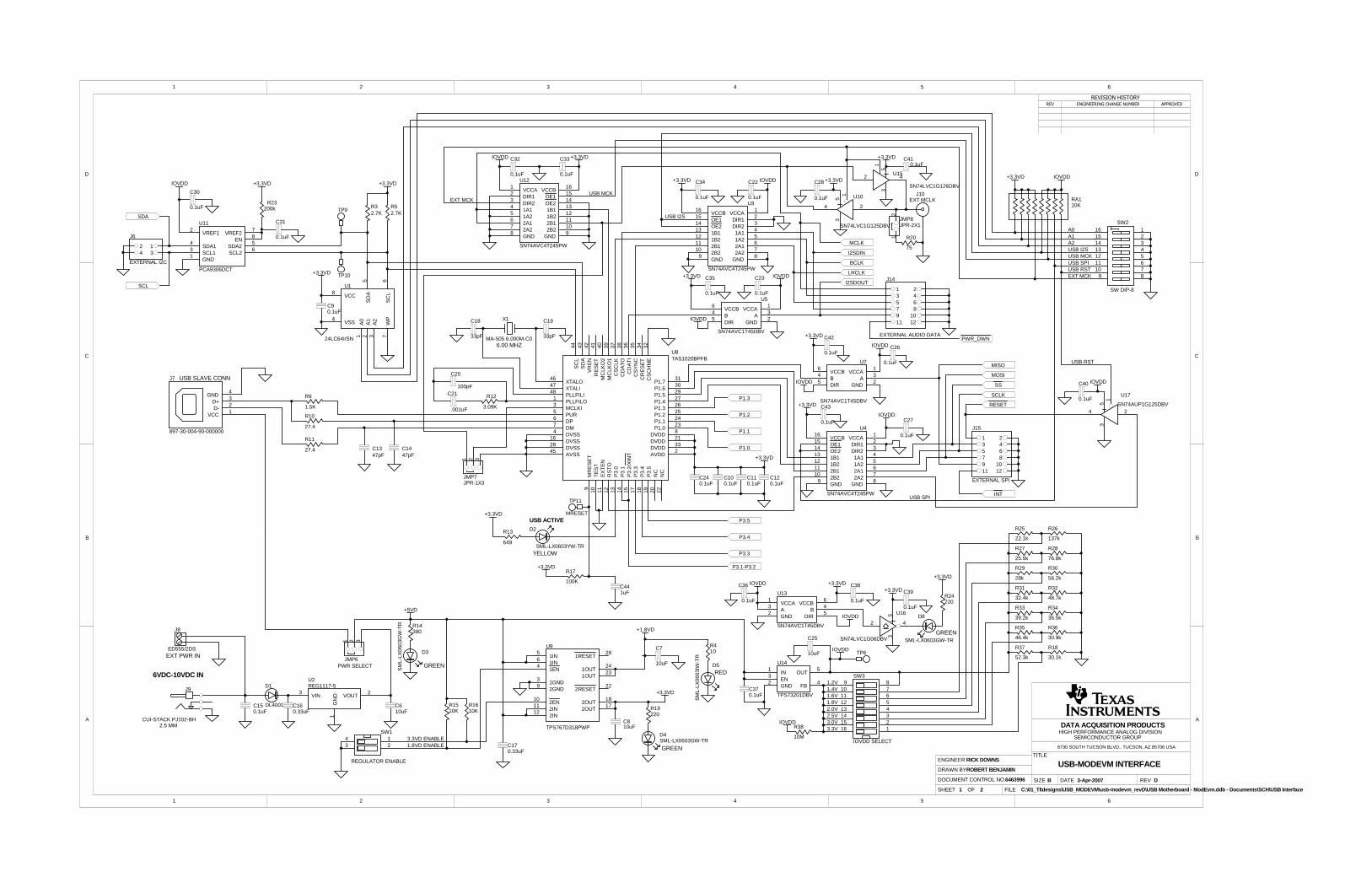
1 2 3 4 5 6
A
B
C
D
654321
D
C
B
Ati
6730 SOUTH TUCSON BLVD., TUCSON, AZ 85706 USA
TITLE
SHEET OF FILE
SIZE DATE REV3-Apr-2007
DRAWN BY
ENGINEER
REVISION HISTORYREV ENGINEERING CHANGE NUMBER APPROVED
B
DATA ACQUISITION PRODUCTSHIGH PERFORMANCE ANALOG DIVISION
SEMICONDUCTOR GROUP
RICK DOWNS
ROBERT BENJAMIN
C:\01_TI\designs\USB_MODEVM\usb-modevm_revD\USB Motherboard - ModEvm.ddb - Documents\SCH\USB Interface
D
1 2
USB-MODEVM INTERFACE
J9
CUI-STACK PJ102-BH
YELLOW
2.5 MM
6VDC-10VDC IN
C150.1uF
DOCUMENT CONTROL NO.
CS
CH
NE
32C
RE
SE
T34
CS
YN
C35
CD
AT
I36
CS
CLK
37M
CLK
O1
39M
CLK
O2
40R
ES
ET
41V
RE
N42
SD
A43
SC
L44
XTALO46
XTALI47
PLLFILI48
PLLFILO1
MCLKI3
PUR5
DP6
DM7
MR
ES
ET
9
DVSS4
DVSS16
DVSS28
AVSS45
TE
ST
10
EX
TE
N11
CD
AT
O38
RS
TO
12
NC
20
NC
22
P3.
013
P3.
114
P3.
2/X
INT
15
P3.
317
P3.
418
P3.
519
AVDD2
DVDD33
DVDD21
DVDD8
P1.023
P1.124
P1.225
P1.326
P1.427
P1.529
P1.630
P1.731
U8TAS1020BPFB
VCC1
D-2
D+3
GND4
J7
897-30-004-90-000000
R9
1.5K
R10
27.4
R11
27.4 C1347pF
C1447pF
1 2 3
JMP6PWR SELECT
C20
100pFC21
.001uF
R12
3.09K
X1
MA-505 6.000M-C0
C18
33pF
C19
33pF
+3.3VD
VCC8
VSS4
SD
A5
SC
L6
A0
1
A1
2
A2
3
WP
7
U1
24LC64I/SN
+3.3VD
C90.1uF
TP9
TP10
R32.7K
R52.7K
+3.3VD
MCLK
BCLK
LRCLK
I2SDIN
I2SDOUT
INT
MISO
MOSI
SS
SCLK
R13
649
+3.3VD
R410
C100.1uF
C110.1uF
C120.1uF
USB SLAVE CONN
EXT PWR IN
6.00 MHZ
6463996
RED
IOVDD
IOVDD
C23
0.1uF
C22
0.1uF
IOVDDC27
0.1uF
+3.3VD
C26
0.1uF
+3.3VD
IOVDD
+3.3VD
IOVDD
TP11
MRESET
3.3VD ENABLE1.8VD ENABLE C17
0.33uF
C7
10uF
1GND3
1EN4
1IN5
1IN6
2GND9
2EN10
2IN11
2IN12
2OUT17
2OUT18
2RESET22
1OUT23
1OUT24
1RESET28
U9
TPS767D318PWP
R17
100K
+3.3VD
C810uF
D5
SM
L-LX
0603
IW-T
R
D2
SML-LX0603YW-TR
D4SML-LX0603GW-TR
R19220
GREEN
USB I2SUSB MCKUSB SPI
USB SPI
USB I2S
USB MCK
+1.8VD
RESET
C240.1uF
USB ACTIVE
USB RST
USB RST
246
1357 89 1011 12
J15
EXTERNAL SPI
246
1357 89 1011 12
J14
EXTERNAL AUDIO DATAPWR_DWN
J10EXT MCLK
R20
75
+3.3VD
12345678
16151413121110
9
SW2
SW DIP-8
EXT MCK
24
13
J6
EXTERNAL I2C
IOVDD
SDA
SCL
+5VD
R1510K
R1610K
1423
SW1
REGULATOR ENABLE
VIN3
VOUT2
GN
D1
U2REG1117-5D1
DL4001 C160.33uF
C610uF
P3.3
P3.4
P3.5
P1.0
P1.1
P1.2
P1.3
J8
ED555/2DSTP6D3
SM
L-LX
0603
GW
-TR R14
390
GREEN
A0A1A2
24
15
3
U10
SN74LVC1G125DBV
C28
0.1uF RA110K
VREF12
VREF27
EN8
GND1
SCL26
SDA25
SCL13
SDA14
U11
PCA9306DCT
C30
0.1uFR23
200k
C31
0.1uF
+3.3VD
IN1
GND2
EN3
OUT5
FB4
U14
TPS73201DBV
11621531441351261171089
SW3
IOVDD SELECT
C25
10uF
1.2V1.4V1.6V1.8V2.0V2.5V3.0V3.3V
R27
25.5k
R29
28k
R35
46.4k
R36
30.9k
R34
36.5k
R32
48.7k
R31
32.4k
R33
39.2k
R25
22.1k
R26
137k
R28
76.8k
R30
56.2k
R18
30.1k
R37
52.3k
C370.1uF
VCCA1
DIR12
1A14
1A25
2A16
2A27
DIR23
GND8
GND9
OE214
2B210
2B111
1B212
1B113
OE115
VCCB16
U3
SN74AVC4T245PW
+3.3VD C34
0.1uF
VCCA1
A3
GND2
VCCB6
B4
DIR5
U7
SN74AVC1T45DBV
C42
0.1uF
VCCA1
A3
GND2
VCCB6
B4
DIR5
U5
SN74AVC1T45DBV
C35
0.1uF
IOVDD
IOVDD
VCCA1
DIR12
1A14
1A25
2A16
2A27
DIR23
GND8
GND9
OE214
2B210
2B111
1B212
1B113
OE115
VCCB16
U12
SN74AVC4T245PW
+3.3VDIOVDD C32
0.1uF
C33
0.1uF
EXT MCK
VCCA1
DIR12
1A14
1A25
2A16
2A27
DIR23
GND8
GND9
OE214
2B210
2B111
1B212
1B113
OE115
VCCB16
U4
SN74AVC4T245PW
C43
0.1uF
+3.3VD24
15
3
U17
SN74AUP1G125DBV
C40
0.1uF
IOVDD
1 2 3JMP7JPR-1X3
12
JMP8JPR-2X1
2 4
15
3
U15
SN74LVC1G126DBV
+3.3VD C410.1uF
VCCA1
A3
GND2
VCCB6
B4
DIR5
U13
SN74AVC1T45DBV
C36
0.1uF
C38
0.1uF
+3.3VDIOVDD
IOVDD
+3.3VD
+3.3VD
C39
0.1uF
D8
SML-LX0603GW-TR
R24220
GREEN
IOVDD
P3.1-P3.2
C441uF
+3.3VD
2 4
53
U16
SN74LVC1G06DBV
R38
10M
IOVDD

www.ti.com
Appendix F USB-MODEVM Bill of Materials
The complete bill of materials for USB-MODEVM Interface Board is provided as a reference.
Table 8. USB-MODEVM Bill of Materials
Designators Description Manufacturer Mfg. Part Number
R4 10Ω 1/10W 5% Chip Resistor Panasonic ERJ-3GEYJ1300V
R10, R11 27.4Ω 1/16W 1% Chip Resistor Panasonic ERJ-3EKF27R4V
R20 75Ω 1/4W 1% Chip Resistor Panasonic ERJ-14NF75R0U
R19 220Ω 1/10W 5% Chip Resistor Panasonic ERJ-3GEYJ221V
R14, R21, R22 390Ω 1/10W 5% Chip Resistor Panasonic ERJ-3GEYJ391V
R13 649Ω 1/16W 1% Chip Resistor Panasonic ERJ-3EKF6490V
R9 1.5KΩ 1/10W 5% Chip Resistor Panasonic ERJ-3GEYJ1352V
R1–R3, R5–R8 2.7KΩ 1/10W 5% Chip Resistor Panasonic ERJ-3GEYJ272V
R12 3.09KΩ 1/16W 1% Chip Resistor Panasonic ERJ-3EKF3091V
R15, R16 10KΩ 1/10W 5% Chip Resistor Panasonic ERJ-3GEYJ1303V
R17, R18 100kΩ 1/10W 5%Chip Resistor Panasonic ERJ-3GEYJ1304V
RA1 10KΩ 1/8W Octal Isolated Resistor Array CTS Corporation 742C163103JTR
C18, C19 33pF 50V Ceramic Chip Capacitor, ±5%, NPO TDK C1608C0G1H330J
C13, C14 47pF 50V Ceramic Chip Capacitor, ±5%, NPO TDK C1608C0G1H470J
C20 100pF 50V Ceramic Chip Capacitor, ±5%, NPO TDK C1608C0G1H101J
C21 1000pF 50V Ceramic Chip Capacitor, ±5%, NPO TDK C1608C0G1H102J
C15 0.1μF 16V Ceramic Chip Capacitor, ±10%, X7R TDK C1608X7R1C104K
C16, C17 0.33μF 16V Ceramic Chip Capacitor, ±20%, Y5V TDK C1608X5R1C334K
C9–C12, C22–C28 1μF 6.3V Ceramic Chip Capacitor, ±10%, X5R TDK C1608X5R0J1305K
C1–C8 10μF 6.3V Ceramic Chip Capacitor, ±10%, X5R TDK C3216X5R0J1306K
D1 50V, 1A, Diode MELF SMD Micro Commercial Components DL4001
D2 Yellow Light Emitting Diode Lumex SML-LX0603YW-TR
D3– D7 Green Light Emitting Diode Lumex SML-LX0603GW-TR
D5 Red Light Emitting Diode Lumex SML-LX0603IW-TR
Q1, Q2 N-Channel MOSFET Zetex ZXMN6A07F
X1 6MHz Crystal SMD Epson MA-505 6.000M-C0
U8 USB Streaming Controller Texas Instruments TAS1020BPFB
U2 5V LDO Regulator Texas Instruments REG1117-5
U9 3.3V/1.8V Dual Output LDO Regulator Texas Instruments TPS767D318PWP
U3, U4 Quad, 3-State Buffers Texas Instruments SN74LVC125APW
U5–U7 Single IC Buffer Driver with Open Drain o/p Texas Instruments SN74LVC1G07DBVR
U10 Single 3-State Buffer Texas Instruments SN74LVC1G125DBVR
U1 Microchip 24LC64I/SN64K 2-Wire Serial EEPROM I2C
USB-MODEVM PCB Texas Instruments 6463995
TP1–TP6, TP9–TP11 Miniature test point terminal Keystone Electronics 5000
TP7, TP8 Multipurpose test point terminal Keystone Electronics 5011
J7 USB Type B Slave Connector Thru-Hole Mill-Max 897-30-004-90-000000
J13, J2–J5, J8 2-position terminal block On Shore Technology ED555/2DS
J9 2.5mm power connector CUI Stack PJ-102B
J130 BNC connector, female, PC mount AMP/Tyco 414305-1
J131A, J132A, J21A, J22A 20-pin SMT plug Samtec TSM-110-01-L-DV-P
J131B, J132B, J21B, J22B 20-pin SMT socket Samtec SSW-110-22-F-D-VS-K
J133A, J23A 10-pin SMT plug Samtec TSM-105-01-L-DV-P
J133B, J23B 10-pin SMT socket Samtec SSW-105-22-F-D-VS-K
J6 4-pin double row header (2x2) 0.1" Samtec TSW-102-07-L-D
J134, J135 12-pin double row header (2x6) 0.1" Samtec TSW-106-07-L-D
JMP1–JMP4 2-position jumper, 0.1" spacing Samtec TSW-102-07-L-S
39SLAU264A–October 2008–Revised September 2012 USB-MODEVM Bill of MaterialsSubmit Documentation Feedback
Copyright © 2008–2012, Texas Instruments Incorporated

Appendix F www.ti.com
Table 8. USB-MODEVM Bill of Materials (continued)
Designators Description Manufacturer Mfg. Part Number
JMP8–JMP14 2-position jumper, 0.1" spacing Samtec TSW-102-07-L-S
JMP5, JMP6 3-position jumper, 0.1" spacing Samtec TSW-103-07-L-S
JMP7 3-position dual row jumper, 0.1" spacing Samtec TSW-103-07-L-D
SW1 SMT, half-pitch 2-position switch C&K Division, ITT TDA02H0SK1
SW2 SMT, half-pitch 8-position switch C&K Division, ITT TDA08H0SK1
Jumper plug Samtec SNT-100-BK-T
40 USB-MODEVM Bill of Materials SLAU264A–October 2008–Revised September 2012Submit Documentation Feedback
Copyright © 2008–2012, Texas Instruments Incorporated

www.ti.com
Appendix G USB-MODEVM Protocol
G.1 USB-MODEVM Protocol
The USB-MODEVM is defined to be a Vendor-Specific class and is identified on the PC system as an NI-VISA device. Because the TAS1020B has several routines in its ROM which are designed for use withHID-class devices, HID-like structures are used, even though the USB-MODEVM is not an HID-classdevice. Data is passed from the PC to the TAS1020B using the control endpoint.
Data is sent in a HIDSETREPORT (see Table 9).
Table 9. USB Control EndpointHIDSETREPORT Request
Part Value Description
bmRequestType 0x21 00100001
bRequest 0x09 SET_REPORT
wValue 0x00 don't care
wIndex 0x03 HID interface is index 3
wLength calculated by host
Data Data packet as described in Table 10.
The data packet consists of the following bytes, shown in Table 10:
Table 10. Data Packet Configuration
BYTE NUMBER TYPE DESCRIPTION
0 Interface Specifies serial interface and operation. The two values are logically ORed.Operation:
READ 0x00WRITE 0x10
Interface:
GPIO 0x08SPI_16 0x04I2C_FAST 0x02I2C_STD 0x01SPI_8 0x00
1 I2C Slave Address Slave address of I2C device or MSB of 16-bit reg addr for SPI
2 Length Length of data to write/read (number of bytes)
3 Register address Address of register for I2C or 8-bit SPI; LSB of 16-bit address for SPI
4..64 Data Up to 60 data bytes could be written at a time. EP0 maximum length is 64. The returnpacket is limited to 42 bytes, so advise only sending 32 bytes at any one time.
Example usage:Write two bytes (AA, 55) to device starting at register 5 of an I2C device with address A0:
[0] 0x11[1] 0xA0[2] 0x02[3] 0x05[4] 0xAA[5] 0x55
41SLAU264A–October 2008–Revised September 2012 USB-MODEVM ProtocolSubmit Documentation Feedback
Copyright © 2008–2012, Texas Instruments Incorporated

USB-MODEVM Protocol www.ti.com
Do the same with a fast mode I2C device:
[0] 0x12[1] 0xA0[2] 0x02[3] 0x05[4] 0xAA[5] 0x55
Now with an SPI device which uses an 8-bit register address:
[0] 0x10[1] 0xA0[2] 0x02[3] 0x05[4] 0xAA[5] 0x55
Now, do a 16-bit register address, as found on parts like the TSC2101. Assume the register address(command word) is 0x10E0:
[0] 0x14[1] 0x10 → Note: the I2C address now serves as MSB of reg addr.[2] 0x02[3] 0xE0[4] 0xAA[5] 0x55
In each case, the TAS1020 returns, in an HID interrupt packet, the following:
[0] interface byte | statusstatus:
REQ_ERROR 0x80
INTF_ERROR 0x40
REQ_DONE 0x20
[1] for I2C interfaces, the I2C address as sentfor SPI interfaces, the read back data from SPI line for transmission of the corresponding byte
[2] length as sent[3] for I2C interfaces, the reg address as sent
for SPI interfaces, the read back data from SPI line for transmission of the corresponding byte[4..60] echo of data packet sent
42 USB-MODEVM Protocol SLAU264A–October 2008–Revised September 2012Submit Documentation Feedback
Copyright © 2008–2012, Texas Instruments Incorporated

www.ti.com USB-MODEVM Protocol
If the command is sent with no problem, the returning byte [0] is the same as the sent one logically ORedwith 0x20 - in the preceding first example, the returning packet is:
[0] 0x31[1] 0xA0[2] 0x02[3] 0x05[4] 0xAA[5] 0x55
If for some reason the interface fails (for example, the I2C device does not acknowledge), it comes backas:
[0] 0x51 → interface | INTF_ERROR[1] 0xA0[2] 0x02[3] 0x05[4] 0xAA[5] 0x55
If the request is malformed, that is, the interface byte (byte [0]) takes on a value which is not as previouslydescribed, the return packet is:
[0] 0x93 → the user sent 0x13, which is not valid, so 0x93 returned[1] 0xA0[2] 0x02[3] 0x05[4] 0xAA[5] 0x55
The preceding examples used writes. Reading is similar:Read two bytes from device starting at register 5 of an I2C device with address A0:
[0] 0x01[1] 0xA0[2] 0x02[3] 0x05
43SLAU264A–October 2008–Revised September 2012 USB-MODEVM ProtocolSubmit Documentation Feedback
Copyright © 2008–2012, Texas Instruments Incorporated
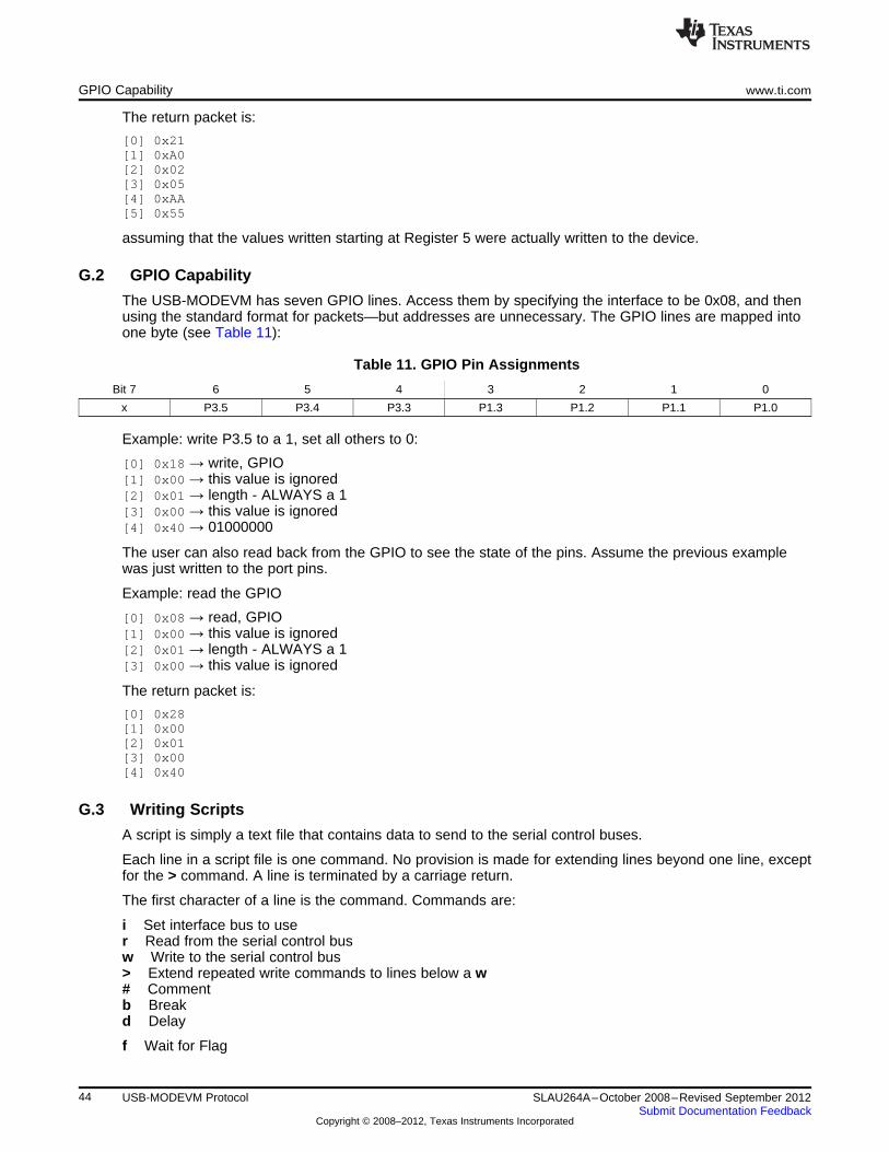
GPIO Capability www.ti.com
The return packet is:
[0] 0x21[1] 0xA0[2] 0x02[3] 0x05[4] 0xAA[5] 0x55
assuming that the values written starting at Register 5 were actually written to the device.
G.2 GPIO Capability
The USB-MODEVM has seven GPIO lines. Access them by specifying the interface to be 0x08, and thenusing the standard format for packets—but addresses are unnecessary. The GPIO lines are mapped intoone byte (see Table 11):
Table 11. GPIO Pin Assignments
Bit 7 6 5 4 3 2 1 0
x P3.5 P3.4 P3.3 P1.3 P1.2 P1.1 P1.0
Example: write P3.5 to a 1, set all others to 0:
[0] 0x18 → write, GPIO[1] 0x00 → this value is ignored[2] 0x01 → length - ALWAYS a 1[3] 0x00 → this value is ignored[4] 0x40 → 01000000
The user can also read back from the GPIO to see the state of the pins. Assume the previous examplewas just written to the port pins.
Example: read the GPIO
[0] 0x08 → read, GPIO[1] 0x00 → this value is ignored[2] 0x01 → length - ALWAYS a 1[3] 0x00 → this value is ignored
The return packet is:
[0] 0x28[1] 0x00[2] 0x01[3] 0x00[4] 0x40
G.3 Writing Scripts
A script is simply a text file that contains data to send to the serial control buses.
Each line in a script file is one command. No provision is made for extending lines beyond one line, exceptfor the > command. A line is terminated by a carriage return.
The first character of a line is the command. Commands are:
i Set interface bus to user Read from the serial control busw Write to the serial control bus> Extend repeated write commands to lines below a w# Commentb Breakd Delay
f Wait for Flag
44 USB-MODEVM Protocol SLAU264A–October 2008–Revised September 2012Submit Documentation Feedback
Copyright © 2008–2012, Texas Instruments Incorporated

www.ti.com Writing Scripts
The first command, i, sets the interface to use for the commands to follow. This command must befollowed by one of the following parameters:
i2cstd Standard mode I2C busi2cfast Fast mode I2C busspi8 SPI bus with 8-bit register addressingspi16 SPI bus with 16-bit register addressinggpio Use the USB-MODEVM GPIO capability
For example, if a fast mode I2C bus is to be used, the script begins with:
i i2cfast
A double quoted string of characters following the b command can be added to provide information to theuser about each breakpoint. When the script is executed, the software's command handler halts as soonas a breakpoint is detected and displays the string of characters within the double quotes.
The Wait for Flag command, f, reads a specified register and verifies if the bitmap provided with thecommand matches the data being read. If the data does not match, the command handler retries for up to200 times. This feature is useful when switching buffers in parts that support the adaptive filtering mode.The command f syntax follows:f [i2c address] [register] [D7][D6][D5][D4][D3][D2][D1][D0] where 'i2c address' and 'register'are in hexadecimal format and 'D7' through 'D0' are in binary format with values of 0, 1 or X fordon't care.
Anything following a comment command # is ignored by the parser, provided that it is on the same line.
The delay command d allows the user to specify a time, in milliseconds, that the script pauses beforeproceeding. The delay time is entered in decimal format.
A series of byte values follows either a read or write command. Each byte value is expressed inhexadecimal, and each byte must be separated by a space. Commands are interpreted and sent to theTAS1020B by the program using the protocol described in Section G.1.
The first byte following an r (read) or w (write) command is the I2C slave address of the device (if I2C isused) or the first data byte to write (if SPI is used—note that SPI interfaces are not standardized onprotocols, so the meaning of this byte varies with the device being addressed on the SPI bus). Thesecond byte is the starting register address that data will be written to (again, with I2C; SPI varies—seeSection G.1 for additional information about what variations may be necessary for a particular SPI mode).Following these two bytes are data, if writing; if reading, the third byte value is the number of bytes toread, (expressed in hexadecimal).
For example, to write the values 0xAA 0x55 to an I2C device with a slave address of 0x30, starting at aregister address of 0x03, the user writes:#example script i i2cfast w 30 03 AA 55 r 30 03 02
This script begins with a comment, specifies that a fast I2C bus will be used, then writes 0xAA 0x55 to theI2C slave device at address 0x30, writing the values into registers 0x03 and 0x04. The script then readsback two bytes from the same device starting at register address 0x03. Note that the slave device valuedoes not change. It is unnecessary to set the R/W bit for I2C devices in the script; the read or writecommands does that.
If extensive repeated write commands are sent and commenting is desired for a group of bytes, the >command can be used to extend the bytes to other lines that follow. A usage example for the > commandfollows:#example script for '>' command i i2cfast # Write AA and BB to registers 3 and 4, respectively w30 03 AA BB # Write CC, DD, EE and FF to registers 5, 6, 7 and 8, respectively > CC DD EE FF #Place a commented breakpoint b "AA BB CC DD EE FF was written, starting at register 3" # Readback all six registers, starting at register 3 r 30 03 06
The following example demonstrates usage of the Wait for Flag command, f:#example script for 'wait for flag' command i i2cfast # Switch to Page 44 w 30 00 2C # Switchbuffers w 30 01 05 # Wait for bit D0 to clear. 'x' denotes a don't care. f 30 01 xxxxxxx0
45SLAU264A–October 2008–Revised September 2012 USB-MODEVM ProtocolSubmit Documentation Feedback
Copyright © 2008–2012, Texas Instruments Incorporated

Writing Scripts www.ti.com
Any text editor can be used to write these scripts; Jedit is an editor that is highly recommended for generalusage. For more information, go to: http://www.jedit.org.
Once the script is written, it can be used in the command window by running the program, and thenselecting Open Script File... from the File menu. Locate the script and open it. The script is then displayedin the command buffer. The user can also edit the script once it is in the buffer and save it by selectingSave Script File... from the File menu.
Once the script is in the command buffer, it can be executed by pressing the Execute Command Bufferbutton. If there are breakpoints in the script, the script executes to that point, and the user is presentedwith a dialog box with a button to press to continue executing the script. When ready to proceed, push thatbutton and the script continues.
46 USB-MODEVM Protocol SLAU264A–October 2008–Revised September 2012Submit Documentation Feedback
Copyright © 2008–2012, Texas Instruments Incorporated

EVALUATION BOARD/KIT IMPORTANT NOTICE
Texas Instruments (TI) provides the enclosed product(s) under the following conditions:
This evaluation board/kit is intended for use for ENGINEERING DEVELOPMENT, DEMONSTRATION, OR EVALUATION PURPOSESONLY and is not considered by TI to be a finished end-product fit for general consumer use. Persons handling the product(s) must haveelectronics training and observe good engineering practice standards. As such, the goods being provided are not intended to be completein terms of required design-, marketing-, and/or manufacturing-related protective considerations, including product safety and environmentalmeasures typically found in end products that incorporate such semiconductor components or circuit boards. This evaluation board/kit doesnot fall within the scope of the European Union directives regarding electromagnetic compatibility, restricted substances (RoHS), recycling(WEEE), FCC, CE or UL, and therefore may not meet the technical requirements of these directives or other related directives.
Should this evaluation board/kit not meet the specifications indicated in the User’s Guide, the board/kit may be returned within 30 days fromthe date of delivery for a full refund. THE FOREGOING WARRANTY IS THE EXCLUSIVE WARRANTY MADE BY SELLER TO BUYERAND IS IN LIEU OF ALL OTHER WARRANTIES, EXPRESSED, IMPLIED, OR STATUTORY, INCLUDING ANY WARRANTY OFMERCHANTABILITY OR FITNESS FOR ANY PARTICULAR PURPOSE.
The user assumes all responsibility and liability for proper and safe handling of the goods. Further, the user indemnifies TI from all claimsarising from the handling or use of the goods. Due to the open construction of the product, it is the user’s responsibility to take any and allappropriate precautions with regard to electrostatic discharge.
EXCEPT TO THE EXTENT OF THE INDEMNITY SET FORTH ABOVE, NEITHER PARTY SHALL BE LIABLE TO THE OTHER FOR ANYINDIRECT, SPECIAL, INCIDENTAL, OR CONSEQUENTIAL DAMAGES.
TI currently deals with a variety of customers for products, and therefore our arrangement with the user is not exclusive.
TI assumes no liability for applications assistance, customer product design, software performance, or infringement of patents orservices described herein.
Please read the User’s Guide and, specifically, the Warnings and Restrictions notice in the User’s Guide prior to handling the product. Thisnotice contains important safety information about temperatures and voltages. For additional information on TI’s environmental and/orsafety programs, please contact the TI application engineer or visit www.ti.com/esh.
No license is granted under any patent right or other intellectual property right of TI covering or relating to any machine, process, orcombination in which such TI products or services might be or are used.
FCC Warning
This evaluation board/kit is intended for use for ENGINEERING DEVELOPMENT, DEMONSTRATION, OR EVALUATION PURPOSESONLY and is not considered by TI to be a finished end-product fit for general consumer use. It generates, uses, and can radiate radiofrequency energy and has not been tested for compliance with the limits of computing devices pursuant to part 15 of FCC rules, which aredesigned to provide reasonable protection against radio frequency interference. Operation of this equipment in other environments maycause interference with radio communications, in which case the user at his own expense will be required to take whatever measures maybe required to correct this interference.
EVM WARNINGS AND RESTRICTIONS
It is important to operate the EVM daughterboard within the input voltage range specified in Table A-4 and the EVM motherboard within theinput voltage range of 6 Vdc to 10 Vdc when using an external ac/dc power source. See the USB-MODEVM Interface Power section of thismanual when using laboratory power supplies.
Exceeding the specified input range may cause unexpected operation and/or irreversible damage to the EVM. If there are questionsconcerning the input range, please contact a TI field representative prior to connecting the input power.
Applying loads outside of the specified output range may result in unintended operation and/or possible permanent damage to the EVM.Please consult the EVM User's Guide prior to connecting any load to the EVM output. If there is uncertainty as to the load specification,please contact a TI field representative.
During normal operation, some circuit components may have case temperatures greater than 85°C. The EVM is designed to operateproperly with certain components above 85°C as long as the input and output ranges are maintained. These components include but arenot limited to linear regulators, switching transistors, pass transistors, and current sense resistors. These types of devices can be identifiedusing the EVM schematic located in the EVM User's Guide. When placing measurement probes near these devices during operation,please be aware that these devices may be very warm to the touch.
Mailing Address: Texas Instruments, Post Office Box 655303, Dallas, Texas 75265Copyright © 2008, Texas Instruments Incorporated

IMPORTANT NOTICE
Texas Instruments Incorporated and its subsidiaries (TI) reserve the right to make corrections, enhancements, improvements and otherchanges to its semiconductor products and services per JESD46, latest issue, and to discontinue any product or service per JESD48, latestissue. Buyers should obtain the latest relevant information before placing orders and should verify that such information is current andcomplete. All semiconductor products (also referred to herein as “components”) are sold subject to TI’s terms and conditions of salesupplied at the time of order acknowledgment.
TI warrants performance of its components to the specifications applicable at the time of sale, in accordance with the warranty in TI’s termsand conditions of sale of semiconductor products. Testing and other quality control techniques are used to the extent TI deems necessaryto support this warranty. Except where mandated by applicable law, testing of all parameters of each component is not necessarilyperformed.
TI assumes no liability for applications assistance or the design of Buyers’ products. Buyers are responsible for their products andapplications using TI components. To minimize the risks associated with Buyers’ products and applications, Buyers should provideadequate design and operating safeguards.
TI does not warrant or represent that any license, either express or implied, is granted under any patent right, copyright, mask work right, orother intellectual property right relating to any combination, machine, or process in which TI components or services are used. Informationpublished by TI regarding third-party products or services does not constitute a license to use such products or services or a warranty orendorsement thereof. Use of such information may require a license from a third party under the patents or other intellectual property of thethird party, or a license from TI under the patents or other intellectual property of TI.
Reproduction of significant portions of TI information in TI data books or data sheets is permissible only if reproduction is without alterationand is accompanied by all associated warranties, conditions, limitations, and notices. TI is not responsible or liable for such altereddocumentation. Information of third parties may be subject to additional restrictions.
Resale of TI components or services with statements different from or beyond the parameters stated by TI for that component or servicevoids all express and any implied warranties for the associated TI component or service and is an unfair and deceptive business practice.TI is not responsible or liable for any such statements.
Buyer acknowledges and agrees that it is solely responsible for compliance with all legal, regulatory and safety-related requirementsconcerning its products, and any use of TI components in its applications, notwithstanding any applications-related information or supportthat may be provided by TI. Buyer represents and agrees that it has all the necessary expertise to create and implement safeguards whichanticipate dangerous consequences of failures, monitor failures and their consequences, lessen the likelihood of failures that might causeharm and take appropriate remedial actions. Buyer will fully indemnify TI and its representatives against any damages arising out of the useof any TI components in safety-critical applications.
In some cases, TI components may be promoted specifically to facilitate safety-related applications. With such components, TI’s goal is tohelp enable customers to design and create their own end-product solutions that meet applicable functional safety standards andrequirements. Nonetheless, such components are subject to these terms.
No TI components are authorized for use in FDA Class III (or similar life-critical medical equipment) unless authorized officers of the partieshave executed a special agreement specifically governing such use.
Only those TI components which TI has specifically designated as military grade or “enhanced plastic” are designed and intended for use inmilitary/aerospace applications or environments. Buyer acknowledges and agrees that any military or aerospace use of TI componentswhich have not been so designated is solely at the Buyer's risk, and that Buyer is solely responsible for compliance with all legal andregulatory requirements in connection with such use.
TI has specifically designated certain components which meet ISO/TS16949 requirements, mainly for automotive use. Components whichhave not been so designated are neither designed nor intended for automotive use; and TI will not be responsible for any failure of suchcomponents to meet such requirements.
Products Applications
Audio www.ti.com/audio Automotive and Transportation www.ti.com/automotive
Amplifiers amplifier.ti.com Communications and Telecom www.ti.com/communications
Data Converters dataconverter.ti.com Computers and Peripherals www.ti.com/computers
DLP® Products www.dlp.com Consumer Electronics www.ti.com/consumer-apps
DSP dsp.ti.com Energy and Lighting www.ti.com/energy
Clocks and Timers www.ti.com/clocks Industrial www.ti.com/industrial
Interface interface.ti.com Medical www.ti.com/medical
Logic logic.ti.com Security www.ti.com/security
Power Mgmt power.ti.com Space, Avionics and Defense www.ti.com/space-avionics-defense
Microcontrollers microcontroller.ti.com Video and Imaging www.ti.com/video
RFID www.ti-rfid.com
OMAP Applications Processors www.ti.com/omap TI E2E Community e2e.ti.com
Wireless Connectivity www.ti.com/wirelessconnectivity
Mailing Address: Texas Instruments, Post Office Box 655303, Dallas, Texas 75265Copyright © 2012, Texas Instruments Incorporated