TLE7368 DS 11 - farnell.com
41
Automotive Power Data Sheet Rev. 2.1, 2010-11-22 TLE7368 Next Generation Micro Controller Supply TLE7368G TLE7368E TLE7368-2E TLE7368-3E
Transcript of TLE7368 DS 11 - farnell.com
Automot ive Power
Data Sheet Rev. 2.1, 2010-11-22
TLE7368Next Generation Micro Controller Supply
TLE7368G TLE7368E TLE7368-2E TLE7368-3E

Data Sheet 2 Rev. 2.1, 2010-11-22
TLE7368
Table of Contents
1 Overview . . . . . . . . . . . . . . . . . . . . . . . . . . . . . . . . . . . . . . . . . . . . . . . . . . . . . . . . . . . . . . . . . . . . . . . 3
2 Block Diagram . . . . . . . . . . . . . . . . . . . . . . . . . . . . . . . . . . . . . . . . . . . . . . . . . . . . . . . . . . . . . . . . . . . 5
3 Pin Configuration . . . . . . . . . . . . . . . . . . . . . . . . . . . . . . . . . . . . . . . . . . . . . . . . . . . . . . . . . . . . . . . . 63.1 Pin Assignment . . . . . . . . . . . . . . . . . . . . . . . . . . . . . . . . . . . . . . . . . . . . . . . . . . . . . . . . . . . . . . . . . . . 63.2 Pin Definitions and Functions TLE7368G . . . . . . . . . . . . . . . . . . . . . . . . . . . . . . . . . . . . . . . . . . . . . . . 6
4 General Product Characteristics . . . . . . . . . . . . . . . . . . . . . . . . . . . . . . . . . . . . . . . . . . . . . . . . . . . . 94.1 Absolute Maximum Ratings . . . . . . . . . . . . . . . . . . . . . . . . . . . . . . . . . . . . . . . . . . . . . . . . . . . . . . . . . 94.2 Functional Range . . . . . . . . . . . . . . . . . . . . . . . . . . . . . . . . . . . . . . . . . . . . . . . . . . . . . . . . . . . . . . . . 124.3 Thermal Resistance . . . . . . . . . . . . . . . . . . . . . . . . . . . . . . . . . . . . . . . . . . . . . . . . . . . . . . . . . . . . . . 124.4 Electrical Characteristics . . . . . . . . . . . . . . . . . . . . . . . . . . . . . . . . . . . . . . . . . . . . . . . . . . . . . . . . . . 13
5 Detailed Internal Circuits Description . . . . . . . . . . . . . . . . . . . . . . . . . . . . . . . . . . . . . . . . . . . . . . . 245.1 Buck Regulator . . . . . . . . . . . . . . . . . . . . . . . . . . . . . . . . . . . . . . . . . . . . . . . . . . . . . . . . . . . . . . . . . . 245.1.1 Buck Regulator Control Scheme . . . . . . . . . . . . . . . . . . . . . . . . . . . . . . . . . . . . . . . . . . . . . . . . . . . 245.1.2 High Side Driver Supply and 100% Duty Cycle Operation . . . . . . . . . . . . . . . . . . . . . . . . . . . . . . . 245.1.3 Electromagnetic Emission Reduction . . . . . . . . . . . . . . . . . . . . . . . . . . . . . . . . . . . . . . . . . . . . . . . 255.1.4 Charge Pump . . . . . . . . . . . . . . . . . . . . . . . . . . . . . . . . . . . . . . . . . . . . . . . . . . . . . . . . . . . . . . . . . . 265.1.5 Buck Converter Protection Circuits . . . . . . . . . . . . . . . . . . . . . . . . . . . . . . . . . . . . . . . . . . . . . . . . . 265.2 Linear Regulators . . . . . . . . . . . . . . . . . . . . . . . . . . . . . . . . . . . . . . . . . . . . . . . . . . . . . . . . . . . . . . . . 265.3 Voltage Tracking Regulators . . . . . . . . . . . . . . . . . . . . . . . . . . . . . . . . . . . . . . . . . . . . . . . . . . . . . . . 265.4 Power Up and Power Down Sequencing . . . . . . . . . . . . . . . . . . . . . . . . . . . . . . . . . . . . . . . . . . . . . . 275.5 Stand-by Regulator . . . . . . . . . . . . . . . . . . . . . . . . . . . . . . . . . . . . . . . . . . . . . . . . . . . . . . . . . . . . . . . 295.6 Overtemperature Protection . . . . . . . . . . . . . . . . . . . . . . . . . . . . . . . . . . . . . . . . . . . . . . . . . . . . . . . . 295.7 Device Enable Function . . . . . . . . . . . . . . . . . . . . . . . . . . . . . . . . . . . . . . . . . . . . . . . . . . . . . . . . . . . 295.8 Reset Function . . . . . . . . . . . . . . . . . . . . . . . . . . . . . . . . . . . . . . . . . . . . . . . . . . . . . . . . . . . . . . . . . . 295.9 Monitoring Circuit . . . . . . . . . . . . . . . . . . . . . . . . . . . . . . . . . . . . . . . . . . . . . . . . . . . . . . . . . . . . . . . . 315.10 Watchdog Circuit . . . . . . . . . . . . . . . . . . . . . . . . . . . . . . . . . . . . . . . . . . . . . . . . . . . . . . . . . . . . . . . . 33
6 Application Information . . . . . . . . . . . . . . . . . . . . . . . . . . . . . . . . . . . . . . . . . . . . . . . . . . . . . . . . . . 356.1 Choosing Components for the Buck Regulator . . . . . . . . . . . . . . . . . . . . . . . . . . . . . . . . . . . . . . . . . 366.2 Setting up LDO1, LDO2 . . . . . . . . . . . . . . . . . . . . . . . . . . . . . . . . . . . . . . . . . . . . . . . . . . . . . . . . . . . 366.3 Setting up of LDO3 . . . . . . . . . . . . . . . . . . . . . . . . . . . . . . . . . . . . . . . . . . . . . . . . . . . . . . . . . . . . . . . 366.4 Setting up the Stand-by Regulator . . . . . . . . . . . . . . . . . . . . . . . . . . . . . . . . . . . . . . . . . . . . . . . . . . . 376.4.1 Stand-by Regulator’s Output Voltage Configuration . . . . . . . . . . . . . . . . . . . . . . . . . . . . . . . . . . . . 37
7 Package Outlines . . . . . . . . . . . . . . . . . . . . . . . . . . . . . . . . . . . . . . . . . . . . . . . . . . . . . . . . . . . . . . . 38
8 Revision History . . . . . . . . . . . . . . . . . . . . . . . . . . . . . . . . . . . . . . . . . . . . . . . . . . . . . . . . . . . . . . . . 40
Table of Contents
Next Generation Micro Controller Supply
TLE7368
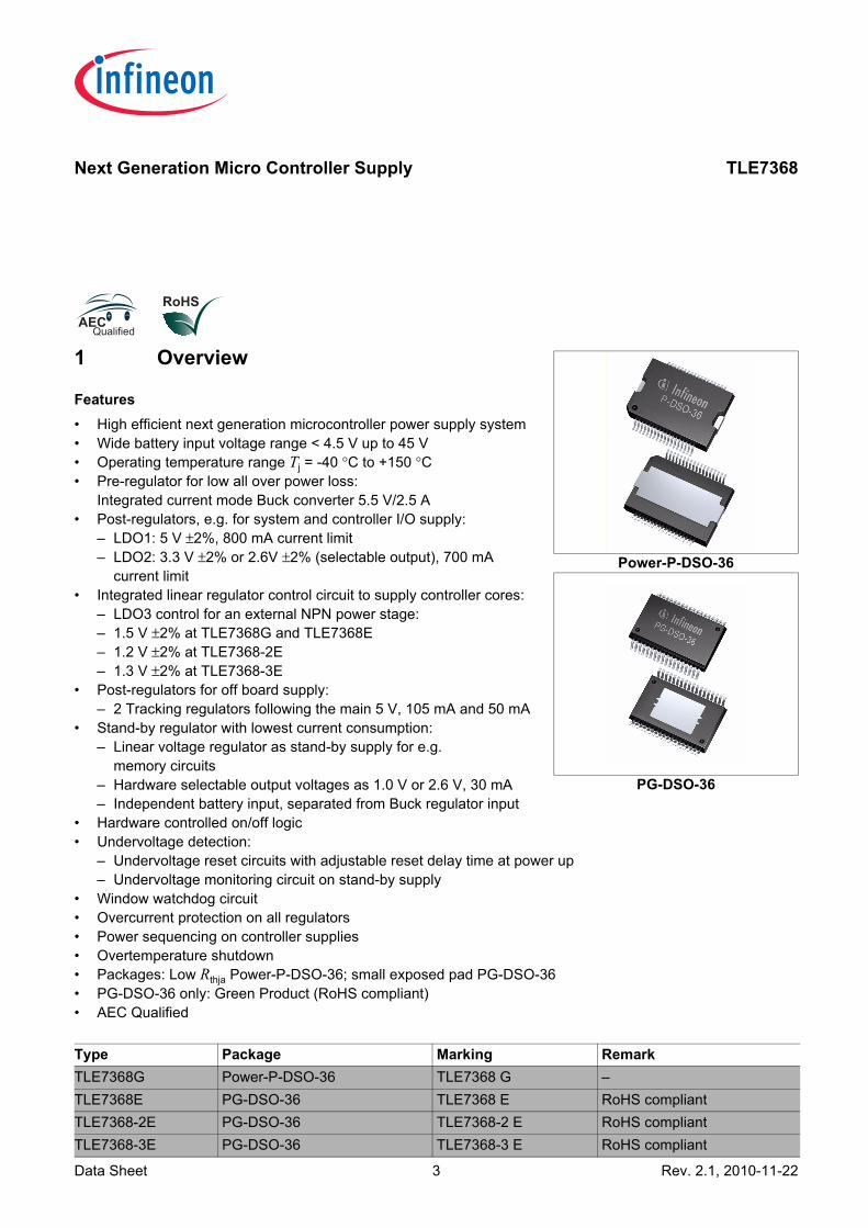
Power-P-DSO-36
PG-DSO-36
1 Overview
Features• High efficient next generation microcontroller power supply system• Wide battery input voltage range < 4.5 V up to 45 V• Operating temperature range Tj = -40 °C to +150 °C• Pre-regulator for low all over power loss:
Integrated current mode Buck converter 5.5 V/2.5 A• Post-regulators, e.g. for system and controller I/O supply:
– LDO1: 5 V ±2%, 800 mA current limit– LDO2: 3.3 V ±2% or 2.6V ±2% (selectable output), 700 mA
current limit• Integrated linear regulator control circuit to supply controller cores:
– LDO3 control for an external NPN power stage:– 1.5 V ±2% at TLE7368G and TLE7368E– 1.2 V ±2% at TLE7368-2E– 1.3 V ±2% at TLE7368-3E
• Post-regulators for off board supply:– 2 Tracking regulators following the main 5 V, 105 mA and 50 mA
• Stand-by regulator with lowest current consumption:– Linear voltage regulator as stand-by supply for e.g.
memory circuits– Hardware selectable output voltages as 1.0 V or 2.6 V, 30 mA– Independent battery input, separated from Buck regulator input
• Hardware controlled on/off logic• Undervoltage detection:
– Undervoltage reset circuits with adjustable reset delay time at power up– Undervoltage monitoring circuit on stand-by supply
• Window watchdog circuit• Overcurrent protection on all regulators• Power sequencing on controller supplies• Overtemperature shutdown• Packages: Low Rthja Power-P-DSO-36; small exposed pad PG-DSO-36• PG-DSO-36 only: Green Product (RoHS compliant)• AEC Qualified
Type Package Marking RemarkTLE7368G Power-P-DSO-36 TLE7368 G –TLE7368E PG-DSO-36 TLE7368 E RoHS compliantTLE7368-2E PG-DSO-36 TLE7368-2 E RoHS compliantTLE7368-3E PG-DSO-36 TLE7368-3 E RoHS compliant
Data Sheet 3 Rev. 2.1, 2010-11-22
TLE7368
Overview
DescriptionThe TLE7368 device is a multifunctional power supply circuit especially designed for Automotive powertrainsystems using a standard 12 V battery. The device is intended to supply and monitor next generation 32-bitmicrocontroller families (13 µm lithography) where voltage levels such as 5 V, 3.3 V or 1.5/1.2/1.3 V are required.The regulator follows the concept of its predecessor TLE6368/SONIC, where the output of a pre-regulator feedsthe inputs of the micro’s linear supplies. In detail, the TLE7368 cascades a Buck converter with linear regulatorsand voltage followers to achieve lowest power dissipation. This configuration allows to power the application evenat high ambient temperatures.The step-down converter delivers a pre-regulated voltage of 5.5 V with a minimum peak current capability of 2.5 A.Supplied by this step down converter two low drop linear post-regulators offer 5 V and 3.3 V (2.6 V) with highaccuracy. The current capability of the regulators is 800 mA and 700 mA. The 3.3 V (2.6 V) linear regulator doeshave its own input allowing to insert a dropper from the Buck output to reduce the on chip power dissipation ifnecessary. For the same reason, reduction of on chip power dissipation, the core supply (1.5 V, 1.2 V or 1.3 V)follows the concept of integrated control circuit with external power stage.Implementing the on board and microcontroller supplies in this way described, allows operation even at highambient temperatures.The regulator system contains the so called power sequencing function which provides a controlled power upsequence of the three output voltages.In addition to the main regulators the inputs of two voltage trackers are connected to the 5.5 V Buck converteroutput voltage. Their protected outputs follow the main 5 V linear regulator with high accuracy and are able to driveloads of 50 mA and 105 mA.To monitor the output voltage levels of each of the linear regulators two independent undervoltage detectioncircuits are available. They can be used to implement the reset or an interrupt function.For energy saving reasons, e.g. while the motor is turned off, the TLE7368 offers a stand-by mode. The standbymode can be enabled and disabled either by battery or the microcontroller. In this stand-by mode just the stand-by regulator remains active and the current drawn from battery is reduced to a minimum for extended batterylifetime. A selection pin allows to configure the output voltages of the stand-by regulator to the application’s needs.The input of the stand-by regulator is separated from the high power input of the pre-/post-regulator system.The TLE7368 is based on Infineon’s Power technology SPT™ which allows bipolar, CMOS and power DMOScircuitry to be integrated on the same monolithic chip/circuitry.
Data Sheet 4 Rev. 2.1, 2010-11-22

TLE7368
Block Diagram
Data Sheet 5 Rev. 2.1, 2010-11-22
2 Block Diagram
Figure 1 Block Diagram
C2-
C1-
C2+
C1+
5.5V
5.0V
2.6/3.3V
1.5/ 1.2/ 1.3V
1.0/2.6V
BST
SWFB/L_INQ_T1
Q_T2
Q_LDO1
IN_LDO2Q_LDO2
SEL_LDO2DRV_EXTFB_EXTWDO
Q_STBY
SEL_STBY
GND_A
MON_STBY
IN_STBYWDI
RO_2
RT
RO_1
EN_µCEN_IGN
IN
CC
P
GND_P
INT.BIASING,CHARGE PUMP
PWMCONTROLLER
ENABLE ≥ 1
RESET(WINDOW
COMPARATOR)
RESET(WINDOW
COMPARATOR)
STANDBYMONITOR
WINDOWWATCHDOG
TEMPERATURESENSE
TLE 7368
TIMING

TLE7368
Pin Configuration
3 Pin Configuration
3.1 Pin Assignment
Figure 2 Pin Configuration
3.2 Pin Definitions and Functions TLE7368G
Pin(TLE7368G)
Pin(TLE7368E)
Symbol Function
1 1 GND_A Analog ground connection; Connect to heatslug resp. exposed pad.
2 2 RT Reset and watchdog timing pin; Connect a ceramic capacitor to GND to determine the time base for the reset delay circuits and the watchdog cycle time
3 3 RO_1 Reset output Q_LDO1;Open drain output, active low. Connect an external 10 kΩ pull-up resistor to microcontroller I/O voltage.
4 4 RO_2 Reset output Q_LDO2 and FB_EXT; Open drain output, active low. Connect an external 10 kΩ pull-up resistor to microcontroller I/O voltage
5 – N.C. Internally not connected; Connect to GND_A
GND_A 1
2
3
RO_2 4
N.C. 5
IN_LDO2 6
Q_LDO2 7
Q_T1 8
CCP
9Q_T2
10EN_uC
11EN_IGN
12SEL_STBY
13C1-
14C2-
15C1+
16C2+
17
GND_P 18 IN19
WDI
20 IN
21 N.C.
22 SEL_Q2
23
SW
24
SW
25
BST
26
FB/L_IN
27
Q_LDO1
28
FB_EXT
29
WDO
30
DRV_EXT31
N.C.32
N.C.33
Q_STBY34
IN_STBY35
MON_STBY36
GND
GND
RT
RO_1
TLE 7368 G
GND_A 1
2
3
RO_2 4
5IN_LDO2
6Q_LDO2
7Q_T1
8
CCP
9
Q_T2
10
EN_uC
11
EN_IGN
12
SEL_STBY
13
C1-
14
C2-
15
C1+
16
C2+
17GND_P
18
IN
19
WDI
20
IN21
GND_A
22
SEL_Q223
SW
24
SW
25
BST
26
FB/L_IN
27
Q_LDO1
28
FB_EXT
29
WDO
30
DRV_EXT
31
32
GND_A
33 Q_STBY
34 IN_STBY
35 MON_STBY
36
RT
RO_1
TLE 7368 EGND_A
IN
Data Sheet 6 Rev. 2.1, 2010-11-22
TLE7368
Pin Configuration
6 5 IN_LDO2 LDO2 input; Connect this pin straight to the Buck converter output or add a dropper in between to reduce power dissipation on the chip.
7 6 Q_LDO2 Voltage regulator 2 output; 3.3 V or 2.6 V, depending on the state of SEL_LDO2. Block to GND with capacitor for stable regulator operation; selection of capacitor CQ_LDO2 according to Chapter 4.4 and Chapter 6.
8 7 Q_T1 Tracking regulator 1 output; Block to GND with capacitor for stable regulator operation; selection of capacitor CQ_T1 according to Chapter 4.4 and Chapter 6.
9 8 Q_T2 Tracking regulator 2 output; Block to GND with capacitor for stable regulator operation; selection of capacitor CQ_T2 according to Chapter 4.4 and Chapter 6.
10 9 EN_uC Enable input microcontroller; High level enables / low level disables the IC except the stand-by regulators;Integrated pull-down resistor
11 10 EN_IGN Enable input ignition line; High level enables / low level disables the IC except the stand-by regulators;Integrated pull-down resistor
12 11 SEL_STBY Selection input for stand-by regulator; Connect to GND to select 2.6 V output voltage for Q_STBY; Connect straight to Q_STBY to select 1.0 V output voltage for Q_STBY
13 12 C1- Charge pump negative #1; Connect a ceramic capacitor 100 nF, to C1+
14 13 C2- Charge pump negative #2; Connect a ceramic capacitor 100 nF, toC2+
15 14 C1+ Charge pump positive #1; Connect a ceramic capacitor 100 nF, to C1-
16 15 C2+ Charge pump positive #2; Connect a ceramic capacitor 100 nF, to C2-
17 16 CCP Charge pump output; Connect a ceramic capacitor, 220 nF, to GND; Used for internal IC supply, do not use for other circuitry.
18 17 GND_P Power ground; Exclusive GND connection of charge pump; Connect this pin to the power ground star point on the PCB.
– 18, 19 GND_A Analog ground connection; Connect to exposed pad.
19, 20 20, 21, 22 IN Buck regulator input; Connect to a pi-filter (or if not used to battery) with short lines; connect filter capacitors in any case with short lines; connect a small ceramic directly at the pin; For details refer to Chapter 6.Interconnect the pins.
21 – N.C. Internally not connected; Connect to GND_A.
Pin(TLE7368G)
Pin(TLE7368E)
Symbol Function
Data Sheet 7 Rev. 2.1, 2010-11-22

TLE7368
Pin Configuration
22 23 SEL_LDO2 Selection input LDO2; Connect to GND to select 2.6 V output voltage for LDO2; Connect straight to Q_LDO2 to select 3.3 V output voltage for LDO2.
23 24 WDI Window Watchdog input; Apply a watchdog trigger signal to this pin
24 25 WDO Window Watchdog output; Open drain output, active low, connect external 10 kΩ pull-up resistor to microcontroller I/O voltage
25, 26 26, 27 SW Buck power stage’s output; Connect both pins directly, on short lines, to the Buck converter circuit, i.e. the catch diode and the Buck inductance
27 28 BST Bootstrap driver supply input; Connect the buck power stage’s driver supply capacitor to the SW pins; For capacitor selection please refer to Chapter 6.
28 29 FB/L_IN Buck converter feedback input plus input for LDO1 and trackers; Connect the output of the buck converter circuit with short lines to these pins; For Buck output capacitor selection please refer to Chapter 6.
29 30 Q_LDO1 Voltage regulator 1 output; 5 V output; Block to GND with capacitor for stable regulator operation; Selection of capacitor CQ_LDO1 according to Chapter 4.4 and Chapter 6.
30 31 FB_EXT External regulator feedback input; Feedback input of control loop for the external power stage regulator. Connect to the emitter of the regulating transistor; Block to GND with capacitor for stable regulator operation; Selection of capacitor CQ_FB_EXT according to Chapter 4.4 and Chapter 6.
31 32 DRV_EXT Bipolar power stage driver output; Connect the base of an external NPN transistor directly to this pin; Regarding choice of the external power stage refer to Chapter 6.
32, 33 – N.C. Internally not connected; Connect to GND_A.34 33 Q_STBY Stand-by regulator output;
Output voltage depending on the state of SEL_STBY; Block to GND with capacitor for stable regulator operation; Selection of capacitor CQ_STBY according to Chapter 4.4 and Chapter 6.
35 34 IN_STBY Input to stand-by regulator; Always connect the reverse polarity protected battery line to this pin; Input to all IC internal biasing circuits; Block to GND directly at the IC with ceramic capacitor; For proper choice of input capacitors please refer to Chapter 6.
36 35 MON_STBY Monitoring output for stand-by regulator; power fail active low output with special timing, open drain, connect external pull-up resistor.
– 36 GND_A Analog ground connection; Connect to exposed pad.
Pin(TLE7368G)
Pin(TLE7368E)
Symbol Function
Data Sheet 8 Rev. 2.1, 2010-11-22
TLE7368
General Product Characteristics
4 General Product Characteristics
4.1 Absolute Maximum Ratings
Absolute Maximum Ratings 1)
Tj = -40 °C to +150 °C; all voltages with respect to ground.Pos. Parameter Symbol Limit Values Unit Conditions
Min. Max.Stand-by Regulator Input IN_STBY4.1.1 Voltage VIN_STBY -0.3 45 V –4.1.2 Current IIN_STBY – – A Limited internallySelection Input SEL_STBY4.1.3 Voltage VSEL_STBY -0.3 5.5 V –4.1.4 Voltage VSEL_STBY -0.3 6.2 V t < 10 s2)
4.1.5 Current ISEL_STBY – – A Limited internallyBuck Regulator Inputs IN4.1.6 Voltage VIN VSW - 0.3 45 V –4.1.7 Voltage VIN -0.3 45 V –4.1.8 Current IIN – – A Limited internallyWatchdog Input WDI4.1.9 Voltage VWDI -0.3 5.5 V –4.1.10 Voltage VWDI -0.3 6.2 V t < 10 s2)
4.1.11 Current IWDI – – A Limited internallyWatchdog Output WDO4.1.12 Voltage VWDO -0.3 5.5 V –4.1.13 Voltage VWDO -0.3 6.2 V t < 10 s2)
4.1.14 Current IWDO – – A Limited internallyCharge Pump Positive C<1+, 2+>4.1.15 Voltage VC<1+, 2+> -0.3 18 V –4.1.16 Current IC<1+, 2+> – – mA –Charge Pump Negative C<1-, 2->4.1.17 Voltage VC<1-, 2-> -0.3 5.5 V –4.1.18 Current IC<1-, 2-> – – mA –Charge Pump Output CCP4.1.19 Voltage VCCP -0.3 18 V –4.1.20 Current ICCP – – mA –Reset Output RO_14.1.21 Voltage VRO_1 -0.3 5.5 V –4.1.22 Voltage VRO_1 -0.3 6.2 V t < 10 s2)
4.1.23 Current IRO_1 – – A Limited internally
Data Sheet 9 Rev. 2.1, 2010-11-22
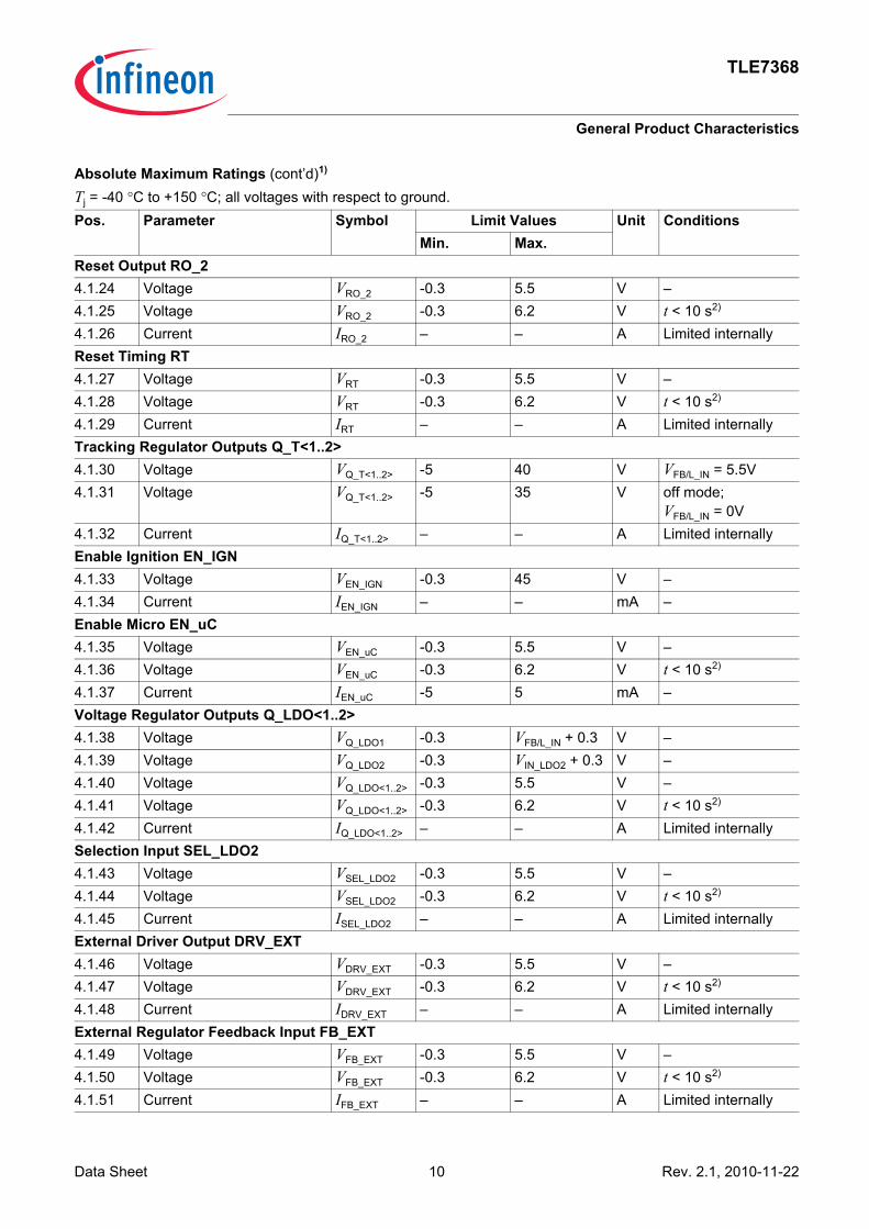
TLE7368
General Product Characteristics
Reset Output RO_24.1.24 Voltage VRO_2 -0.3 5.5 V –4.1.25 Voltage VRO_2 -0.3 6.2 V t < 10 s2)
4.1.26 Current IRO_2 – – A Limited internallyReset Timing RT4.1.27 Voltage VRT -0.3 5.5 V –4.1.28 Voltage VRT -0.3 6.2 V t < 10 s2)
4.1.29 Current IRT – – A Limited internallyTracking Regulator Outputs Q_T<1..2>4.1.30 Voltage VQ_T<1..2> -5 40 V VFB/L_IN = 5.5V4.1.31 Voltage VQ_T<1..2> -5 35 V off mode;
VFB/L_IN = 0V4.1.32 Current IQ_T<1..2> – – A Limited internallyEnable Ignition EN_IGN4.1.33 Voltage VEN_IGN -0.3 45 V –4.1.34 Current IEN_IGN – – mA –Enable Micro EN_uC4.1.35 Voltage VEN_uC -0.3 5.5 V –4.1.36 Voltage VEN_uC -0.3 6.2 V t < 10 s2)
4.1.37 Current IEN_uC -5 5 mA –Voltage Regulator Outputs Q_LDO<1..2>4.1.38 Voltage VQ_LDO1 -0.3 VFB/L_IN + 0.3 V –4.1.39 Voltage VQ_LDO2 -0.3 VIN_LDO2 + 0.3 V –4.1.40 Voltage VQ_LDO<1..2> -0.3 5.5 V –4.1.41 Voltage VQ_LDO<1..2> -0.3 6.2 V t < 10 s2)
4.1.42 Current IQ_LDO<1..2> – – A Limited internallySelection Input SEL_LDO24.1.43 Voltage VSEL_LDO2 -0.3 5.5 V –4.1.44 Voltage VSEL_LDO2 -0.3 6.2 V t < 10 s2)
4.1.45 Current ISEL_LDO2 – – A Limited internallyExternal Driver Output DRV_EXT4.1.46 Voltage VDRV_EXT -0.3 5.5 V –4.1.47 Voltage VDRV_EXT -0.3 6.2 V t < 10 s2)
4.1.48 Current IDRV_EXT – – A Limited internallyExternal Regulator Feedback Input FB_EXT4.1.49 Voltage VFB_EXT -0.3 5.5 V –4.1.50 Voltage VFB_EXT -0.3 6.2 V t < 10 s2)
4.1.51 Current IFB_EXT – – A Limited internally
Absolute Maximum Ratings (cont’d)1)
Tj = -40 °C to +150 °C; all voltages with respect to ground.Pos. Parameter Symbol Limit Values Unit Conditions
Min. Max.
Data Sheet 10 Rev. 2.1, 2010-11-22
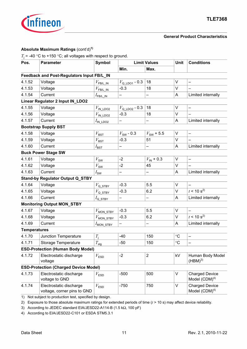
TLE7368
General Product Characteristics
Feedback and Post-Regulators Input FB/L_IN4.1.52 Voltage VFB/L_IN VQ_LDO1 - 0.3 18 V –4.1.53 Voltage VFB/L_IN -0.3 18 V –4.1.54 Current IFB/L_IN – – A Limited internallyLinear Regulator 2 Input IN_LDO24.1.55 Voltage VIN_LDO2 VQ_LDO2 - 0.3 18 V –4.1.56 Voltage VIN_LDO2 -0.3 18 V –4.1.57 Current IIN_LDO2 – – A Limited internallyBootstrap Supply BST4.1.58 Voltage VBST VSW - 0.3 VSW + 5.5 V –4.1.59 Voltage VBST -0.3 51 V –4.1.60 Current IBST – – A Limited internallyBuck Power Stage SW4.1.61 Voltage VSW -2 VIN + 0.3 V –4.1.62 Voltage VSW -2 45 V –4.1.63 Current ISW – – A Limited internallyStand-by Regulator Output Q_STBY4.1.64 Voltage VQ_STBY -0.3 5.5 V –4.1.65 Voltage VQ_STBY -0.3 6.2 V t < 10 s2)
4.1.66 Current IQ_STBY – – A Limited internallyMonitoring Output MON_STBY4.1.67 Voltage VMON_STBY -0.3 5.5 V –4.1.68 Voltage VMON_STBY -0.3 6.2 V t < 10 s2)
4.1.69 Current IMON_STBY – – A Limited internallyTemperatures4.1.70 Junction Temperature Tj -40 150 °C –4.1.71 Storage Temperature Tstg -50 150 °C –ESD-Protection (Human Body Model)4.1.72 Electrostatic discharge
voltageVESD -2 2 kV Human Body Model
(HBM)3)
ESD-Protection (Charged Device Model)4.1.73 Electrostatic discharge
voltage to GNDVESD -500 500 V Charged Device
Model (CDM)4)
4.1.74 Electrostatic discharge voltage, corner pins to GND
VESD -750 750 V Charged Device Model (CDM)4)
1) Not subject to production test, specified by design.2) Exposure to those absolute maximum ratings for extended periods of time (t > 10 s) may affect device reliability.3) According to JEDEC standard EIA/JESD22-A114-B (1.5 kΩ, 100 pF)4) According to EIA/JESD22-C101 or ESDA STM5.3.1
Absolute Maximum Ratings (cont’d)1)
Tj = -40 °C to +150 °C; all voltages with respect to ground.Pos. Parameter Symbol Limit Values Unit Conditions
Min. Max.
Data Sheet 11 Rev. 2.1, 2010-11-22

TLE7368
General Product Characteristics
Note: Stresses above the ones listed here may cause permanent damage to the device. Exposure to absolute maximum rating conditions for extended periods may affect device reliability.
Note: Integrated protection functions are designed to prevent IC destruction under fault conditions described in the data sheet. Fault conditions are considered as “outside” normal operating range. Protection functions are not designed for continuous repetitive operation.
4.2 Functional Range
Note: Within the functional range the IC operates as described in the circuit description. The electrical characteristics are specified within the conditions given in the related electrical characteristics table.
4.3 Thermal Resistance
Pos. Parameter Symbol Limit Values Unit ConditionsMin. Max.
4.2.1 Stand-by input voltage VIN_STBY 3.0 45 V 1)
1) At minimum battery voltage regulators with higher nominal output voltage will not be able to provide the full output voltage. Their outputs follow the battery with certain drop.
4.2.2 Buck input voltage VIN 4.5 45 V 1)
4.2.3 Peak to peak ripple voltage at FB/L_IN
VFB/L_IN 0 150 mVpp –
4.2.4 Junction temperature Tj -40 150 °C –
Pos. Parameter Symbol Limit Values Unit ConditionsMin. Typ. Max.
Power-P-DSO-364.3.1 Junction to ambient RthJA – 49 – K/W Footprint only1)
1) Worst case regarding peak temperature; zero airflow; mounted on FR4; 80 × 80 × 1.5 mm3; 35µ Cu; 5µ Sn
4.3.2 Junction to ambient RthJA – 39 – K/W Heat sink area 300mm2 1)
4.3.3 Junction to ambient RthJA – 32 – K/W Heat sink area 600mm2 1)
4.3.4 Junction to case RthJC – 4.4 – K/W –PG-DSO-364.3.5 Junction to ambient RthJA – 54 – K/W Footprint only1)
4.3.6 Junction to ambient RthJA – 42 – K/W Heat sink area 300mm2 1)
4.3.7 Junction to ambient RthJA – 35 – K/W Heat sink area 600mm2 1)
4.3.8 Junction to case RthJC – 5.6 – K/W –
Data Sheet 12 Rev. 2.1, 2010-11-22

TLE7368
General Product Characteristics
4.4 Electrical Characteristics
Electrical CharacteristicsVIN = VIN_STBY = 13.5 V, Tj = -40 °C to +150 °C, VCCP = 9.0 V; SEL_STBY = Q_STBY; all voltages with respect to ground.Pos. Parameter Symbol Limit Values Unit Conditions
Min. Typ. Max.Buck Regulator4.4.1 Switching frequency f 280 370 425 kHz –4.4.2 Current transition
rise/fall timetr, I – 50 – ns 1); slope magnitude 1 A; fixed
internally4.4.3 Power stage on
resistanceRON, Buck – – 280 mΩ –
4.4.4 Power stage peak current limit
Ipeak, SW 2.5 – 4.6 A VIN = 5.0 V;VSW ramped down from 5.0 V to 3.7 V;VFB/L_IN = 5.0 V
4.4.5 Buck converter output voltage
VFB/L_IN 5.4 – 6.0 V IBuck = 2.0 A2)
4.4.6 Buck converter output voltage
VFB/L_IN 5.4 – 6.4 V IBuck = 100 mA2)
4.4.7 Buck converter, turn on threshold
VIN, on – – 4.5 V VIN increasing
4.4.8 Buck converter, turn off threshold
VIN, off 3.5 – – V VIN decreasing
4.4.9 Buck converter On/off hysteresis
VIN, hyst 450 500 550 mV VIN, hyst = VIN, on - VIN, off
4.4.10 Bootstrap undervoltage lockout, turn on threshold
VBST_UV, on – – VSW + 5.0
V Bootstrap voltage increasing
4.4.11 Bootstrap undervoltage lockout, turn off threshold
VBST_UV, off VSW + 3.2
– – V Bootstrap voltage decreasing
4.4.12 Bootstrap undervoltage lockout, hysteresis
VBST_UV, hyst 0.2 – 1 V VBST_UV, hyst =VBST_UV, on - VBST_UV, off
Charge Pump4.4.13 Charge pump voltage VCCP 9 – 15 V CC1 = 100 nF;
CC2 = 100 nF;CCCP = 220 nF
4.4.14 Charge pump voltage VCCP 9 – 13.5 V VIN = 4.5 V;CC1 = 100 nF;CC2 = 100 nF;CCCP = 220 nF
4.4.15 Charge pump switching frequency
fCCP 1.0 – 2.5 MHz –
Data Sheet 13 Rev. 2.1, 2010-11-22

TLE7368
General Product Characteristics
Voltage Regulator Q_LDO14.4.16 Output voltage VQ_LDO1 4.9 – 5.1 V 1 mA < IQ_LDO1 < 700 mA3)
4.4.17 Output current limitation IQ_LDO1, lim 800 – 1600 mA VQ_LDO1 = 4.0 V4.4.18 Drop voltage Vdr, Q_LDO1 – – 400 mV IQ_LDO1 = 500 mA;
VFB/L_IN = 5.0 V;3) 4)
4.4.19 – – 400 mV IQ_LDO1 = 250 mA;VIN = 4.5 V;3) 4)
4.4.20 Load regulation ∆VQ_LDO1 – 60 120 mV/A –4.4.21 Power supply ripple
rejectionPSRRQ_LD O1 26 – – dB VFB/L_IN = 5.6 V;
VFB/L_IN, ripple pp = 150 mV;fFB/L_IN, ripple = 370 kHz;IQ_LDO1 = 250 mA;CQ_LDO1 = 4.7 µF, X7R1)
4.4.22 Output capacitor CQ_LDO1 1 – 470 µF 1) 5)
4.4.23 Output capacitor ESR CQ_LDO1
0 – 2 Ω at 10 kHz1)
Voltage Regulator Q_LDO24.4.24 Output voltage VQ_LDO2 3.23 – 3.37 V SEL_LDO2 = Q_LDO2;
IN_LDO2 = FB/L_IN; 1 mA < IQ_LDO2 < 500 mA
4.4.25 Output current limitation IQ_LDO2, lim 700 – 1400 mA SEL_LDO2 = Q_LDO2; IN_LDO2 = FB/L_IN;VQ_LDO2 = 2.8 V
4.4.26 Drop voltage Vdr, Q_LDO2 – – 400 mV SEL_LDO2 = Q_LDO2;VCCP = 9 V;IQ_LDO2 = 500 mA;4) 6)
4.4.27 Drop voltage Vdr, Q_LDO2 – – 400 mV SEL_LDO2 = Q_LDO2;VCCP = 9 V;IQ_LDO2 = 250 mA;VIN = 4.5 V;4) 6)
4.4.28 Load regulation ∆VQ_LDO2 – – 80 mV/A 3.3 V mode1 mA < IQ_LDO2 < 650 mA
4.4.29 Output voltage VQ_LDO2 2.56 – 2.67 V SEL_LDO2 = GND;IN_LDO2 = FB/L_IN; 1 mA < IQ_LDO2 < 500 mA
4.4.30 Output current limitation IQ_LDO2, lim 700 – 1400 mA SEL_LDO2 = GND;IN_LDO2 = FB/L_IN;VQ_LDO2 = 2.0 V
4.4.31 Drop voltage Vdr, Q_LDO2 – – 400 mV SEL_LDO2 = GND;VCCP = 9 V;IQ_LDO2 = 500 mA;4)6)
Electrical Characteristics (cont’d)VIN = VIN_STBY = 13.5 V, Tj = -40 °C to +150 °C, VCCP = 9.0 V; SEL_STBY = Q_STBY; all voltages with respect to ground.Pos. Parameter Symbol Limit Values Unit Conditions
Min. Typ. Max.
Data Sheet 14 Rev. 2.1, 2010-11-22
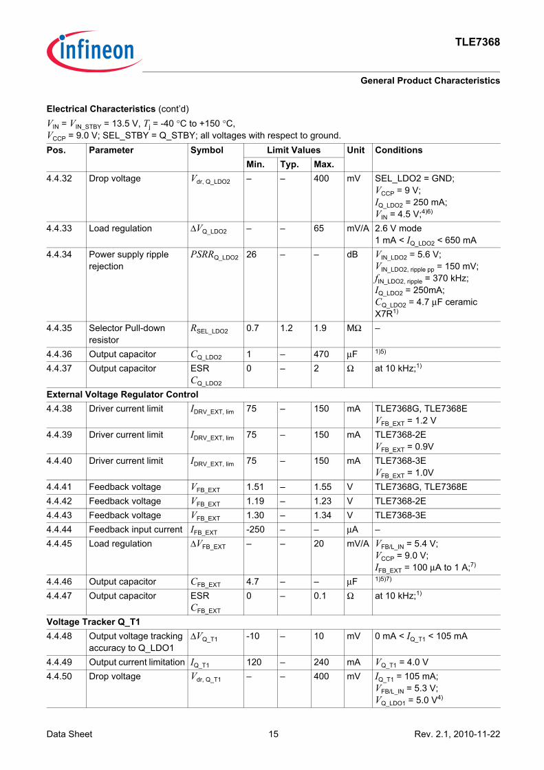
TLE7368
General Product Characteristics
4.4.32 Drop voltage Vdr, Q_LDO2 – – 400 mV SEL_LDO2 = GND;VCCP = 9 V;IQ_LDO2 = 250 mA;VIN = 4.5 V;4)6)
4.4.33 Load regulation ∆VQ_LDO2 – – 65 mV/A 2.6 V mode1 mA < IQ_LDO2 < 650 mA
4.4.34 Power supply ripple rejection
PSRRQ_LDO2 26 – – dB VIN_LDO2 = 5.6 V;VIN_LDO2, ripple pp = 150 mV;fIN_LDO2, ripple = 370 kHz;IQ_LDO2 = 250mA;CQ_LDO2 = 4.7 µF ceramic X7R1)
4.4.35 Selector Pull-down resistor
RSEL_LDO2 0.7 1.2 1.9 MΩ –
4.4.36 Output capacitor CQ_LDO2 1 – 470 µF 1)5)
4.4.37 Output capacitor ESR CQ_LDO2
0 – 2 Ω at 10 kHz;1)
External Voltage Regulator Control4.4.38 Driver current limit IDRV_EXT, lim 75 – 150 mA TLE7368G, TLE7368E
VFB_EXT = 1.2 V4.4.39 Driver current limit IDRV_EXT, lim 75 – 150 mA TLE7368-2E
VFB_EXT = 0.9V4.4.40 Driver current limit IDRV_EXT, lim 75 – 150 mA TLE7368-3E
VFB_EXT = 1.0V4.4.41 Feedback voltage VFB_EXT 1.51 – 1.55 V TLE7368G, TLE7368E4.4.42 Feedback voltage VFB_EXT 1.19 – 1.23 V TLE7368-2E4.4.43 Feedback voltage VFB_EXT 1.30 – 1.34 V TLE7368-3E4.4.44 Feedback input current IFB_EXT -250 – – µA –4.4.45 Load regulation ∆VFB_EXT – – 20 mV/A VFB/L_IN = 5.4 V;
VCCP = 9.0 V;IFB_EXT = 100 µA to 1 A;7)
4.4.46 Output capacitor CFB_EXT 4.7 – – µF 1)5)7)
4.4.47 Output capacitor ESR CFB_EXT
0 – 0.1 Ω at 10 kHz;1)
Voltage Tracker Q_T14.4.48 Output voltage tracking
accuracy to Q_LDO1∆VQ_T1 -10 – 10 mV 0 mA < IQ_T1 < 105 mA
4.4.49 Output current limitation IQ_T1 120 – 240 mA VQ_T1 = 4.0 V4.4.50 Drop voltage Vdr, Q_T1 – – 400 mV IQ_T1 = 105 mA;
VFB/L_IN = 5.3 V;VQ_LDO1 = 5.0 V4)
Electrical Characteristics (cont’d)VIN = VIN_STBY = 13.5 V, Tj = -40 °C to +150 °C, VCCP = 9.0 V; SEL_STBY = Q_STBY; all voltages with respect to ground.Pos. Parameter Symbol Limit Values Unit Conditions
Min. Typ. Max.
Data Sheet 15 Rev. 2.1, 2010-11-22

TLE7368
General Product Characteristics
4.4.51 Power supply ripple rejection
PSRRQ_T1 26 – – dB VFB/L_IN = 5.6 V;VFB/L_IN, ripple pp = 150 mV;fFB/L_IN, ripple = 370 kHz;VQ_LDO1 = 5.0 V;IQ_T1 = 100 mA;CQ_T1 = 4.7µF ceramic X7R;1)
4.4.52 Output capacitor CQ_T1 4.7 – – µF 1)5)
4.4.53 Output capacitor ESR CQ_T1 0 – 3 Ω at 10 kHz;1)
Voltage Tracker Q_T24.4.54 Output voltage tracking
accuracy to Q_LDO1∆VQ_T2 -10 – 10 mV 0 mA < IQ_T2 < 50 mA;
4.4.55 Output current limitation IQ_T2 60 – 110 mA VQ_T2 = 4.0 V4.4.56 Drop voltage Vdr, Q_T2 – – 400 mV IQ_T2 = 50 mA;
VFB/L_IN = 5.3 V;VQ_LDO1 = 5.0 V4)
4.4.57 Power supply ripple rejection
PSRRQ_T2 26 – – dB VFB/L_IN = 5.6 V;VFB/L_IN, ripple pp = 150 mV;fFB/L_IN, ripple = 370 kHz;VQ_LDO1 = 5.0 V;IQ_T2 = 40 mA;CQ_T2 = 4.7 µF ceramic X7R;1)
4.4.58 Output capacitor CQ_T2 4.7 – – µF 1)5)
4.4.59 Output capacitor ESR CQ_T2 0 – 3 Ω at 10 kHz;1)
Stand-by Regulator4.4.60 Output voltage VQ_STBY 0.93 1.02 1.08 V VIN_STBY > 3 V;
100 µA < IQ_STBY < 10 mA; SEL_STBY = Q_STBY
4.4.61 Output voltage VQ_STBY 0.93 1.02 1.08 V VIN_STBY > 4.5 V;IQ_STBY = 30 mA;SEL_STBY = Q_STBY
4.4.62 Output voltage VQ_STBY 2.51 2.62 2.73 V VIN_STBY > 3.0 V;100 µA < IQ_STBY < 10 mA; SEL_STBY = GND
4.4.63 Selector pull-up current ISEL_STBY -2 -5 -10 µA SEL_STBY = GND4.4.64 Output current limitation IQ_STBY, lim 31 – 90 mA VQ_ STBY = 0.5 V
Electrical Characteristics (cont’d)VIN = VIN_STBY = 13.5 V, Tj = -40 °C to +150 °C, VCCP = 9.0 V; SEL_STBY = Q_STBY; all voltages with respect to ground.Pos. Parameter Symbol Limit Values Unit Conditions
Min. Typ. Max.
Data Sheet 16 Rev. 2.1, 2010-11-22
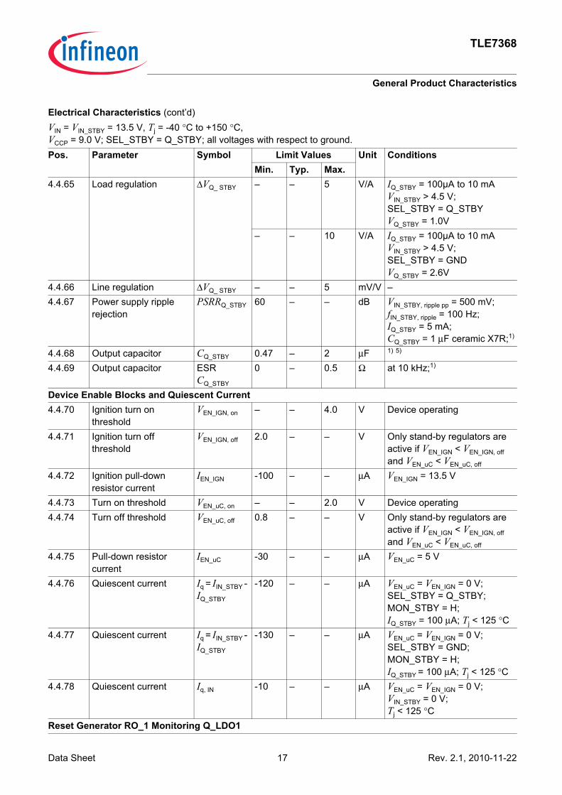
TLE7368
General Product Characteristics
4.4.65 Load regulation ∆VQ_ STBY – – 5 V/A IQ_STBY = 100µA to 10 mAVIN_STBY > 4.5 V;SEL_STBY = Q_STBYVQ_STBY = 1.0V
– – 10 V/A IQ_STBY = 100µA to 10 mAVIN_STBY > 4.5 V;SEL_STBY = GNDVQ_STBY = 2.6V
4.4.66 Line regulation ∆VQ_ STBY – – 5 mV/V –4.4.67 Power supply ripple
rejectionPSRRQ_STBY 60 – – dB VIN_STBY, ripple pp = 500 mV;
fIN_STBY, ripple = 100 Hz;IQ_STBY = 5 mA;CQ_STBY = 1 µF ceramic X7R;1)
4.4.68 Output capacitor CQ_STBY 0.47 – 2 µF 1) 5)
4.4.69 Output capacitor ESR CQ_STBY
0 – 0.5 Ω at 10 kHz;1)
Device Enable Blocks and Quiescent Current4.4.70 Ignition turn on
thresholdVEN_IGN, on – – 4.0 V Device operating
4.4.71 Ignition turn off threshold
VEN_IGN, off 2.0 – – V Only stand-by regulators are active if VEN_IGN < VEN_IGN, off and VEN_uC < VEN_uC, off
4.4.72 Ignition pull-down resistor current
IEN_IGN -100 – – µA VEN_IGN = 13.5 V
4.4.73 Turn on threshold VEN_uC, on – – 2.0 V Device operating4.4.74 Turn off threshold VEN_uC, off 0.8 – – V Only stand-by regulators are
active if VEN_IGN < VEN_IGN, off and VEN_uC < VEN_uC, off
4.4.75 Pull-down resistor current
IEN_uC -30 – – µA VEN_uC = 5 V
4.4.76 Quiescent current Iq = IIN_STBY - IQ_STBY
-120 – – µA VEN_uC = VEN_IGN = 0 V; SEL_STBY = Q_STBY;MON_STBY = H;IQ_STBY = 100 µA; Tj < 125 °C
4.4.77 Quiescent current Iq = IIN_STBY - IQ_STBY
-130 – – µA VEN_uC = VEN_IGN = 0 V; SEL_STBY = GND;MON_STBY = H;IQ_STBY = 100 µA; Tj < 125 °C
4.4.78 Quiescent current Iq, IN -10 – – µA VEN_uC = VEN_IGN = 0 V; VIN_STBY = 0 V;Tj < 125 °C
Reset Generator RO_1 Monitoring Q_LDO1
Electrical Characteristics (cont’d)VIN = VIN_STBY = 13.5 V, Tj = -40 °C to +150 °C, VCCP = 9.0 V; SEL_STBY = Q_STBY; all voltages with respect to ground.Pos. Parameter Symbol Limit Values Unit Conditions
Min. Typ. Max.
Data Sheet 17 Rev. 2.1, 2010-11-22
TLE7368
General Product Characteristics
4.4.79 Undervoltage Reset threshold on Q_LDO1
VURT Q_LDO1,
de
4.50 – 4.75 V VQ_LDO1 decreasing;VFB/L_IN = open;
4.4.80 Undervoltage Reset threshold on Q_LDO1
VURT Q_LDO1,
in
4.55 – 4.90 V VQ_LDO1 increasing
4.4.81 Undervoltage Reset hysteresis
VURO_1, hyst 100 – 220 mV –
4.4.82 Overvoltage Reset threshold on Q_LDO1
VORT Q_LDO1,
in
5.40 – 5.65 V VQ_LDO1 increasing
4.4.83 Overvoltage Reset threshold on Q_LDO1
VORT Q_LDO1,
de
5.25 – 5.60 V VQ_LDO1 decreasing
4.4.84 Overvoltage Reset hysteresis
VORO_1, hyst 80 – 180 mV –
4.4.85 RO_1, Reset output low voltage
VRO_1, low – – 0.4 V IRO_1 = -10 mA;VQ_LDO1 > 2.5 V
4.4.86 RO_1, Reset output low voltage
VRO_1, low – – 0.25 V VIN_STBY = 3.0 V;VQ_LDO1 = 2.5V;IRO_1 = -500 µA;
4.4.87 RO_1, Reset output leakage
IRO_1, high -1 – 1 µA VRO_1 = 5.0 V
4.4.88 Reset delay time base Tcycle 41.6 50 62.5 µs CRT = 1 nF4.4.89 Reset timing capacitor
rangeCRT 0.33 1.0 4.7 nF –
4.4.90 Reset delay time RO_1 tRD, RO_1 – 160 – Tcycle –4.4.91 Undervoltage Reset
reaction timetUVRR, RO_1 2 – 10 µs Voltage step at Q_LDO1 from
5.00 V to 4.48 V4.4.92 Overvoltage Reset
reaction timetOVRR, RO_1 20 – 80 µs Buck converter operating;
Voltage step at Q_LDO1 from 5.00 V to 5.67 V
Reset Generator RO_2 Monitoring Q_LDO2 and FB_EXT4.4.93 Undervoltage Reset
threshold on Q_LDO2VURT Q_LDO2,
de
3.135 – 3.230 V SEL_LDO2 = Q_LDO2;VQ_LDO2 decreasing;VIN_LDO2 = open
4.4.94 Undervoltage Reset headroom on Q_LDO2
VURT Q_LDO2,
head
55 117.5 – mV SEL_LDO2 = Q_LDO2;VURT Q_LDO2, head = VQ_LDO2 - VURT Q_LDO2, de;VQ_LDO2 @ IQ_LDO2 = 500 mA
4.4.95 Undervoltage Reset hysteresis Q_LDO2
VURO_2, hyst 15 – 55 mV SEL_LDO2 = Q_LDO2; VURO_2, hyst = VURT Q_LDO2, in - VURT Q_LDO2, de
4.4.96 Overvoltage Reset threshold on Q_LDO2
VORT Q_LDO2,
in
3.70 – 3.85 V SEL_LDO2 = Q_LDO2;VQ_LDO2 increasing
Electrical Characteristics (cont’d)VIN = VIN_STBY = 13.5 V, Tj = -40 °C to +150 °C, VCCP = 9.0 V; SEL_STBY = Q_STBY; all voltages with respect to ground.Pos. Parameter Symbol Limit Values Unit Conditions
Min. Typ. Max.
Data Sheet 18 Rev. 2.1, 2010-11-22
TLE7368
General Product Characteristics
4.4.97 Overvoltage Reset threshold on Q_LDO2
VORT Q_LDO2,
de
3.55 – 3.80 V SEL_LDO2 = Q_LDO2;VQ_LDO2 decreasing
4.4.98 Overvoltage Reset hysteresis
VORO_2, hyst 50 – 200 mV SEL_LDO2 = Q_LDO2;
4.4.99 Undervoltage Reset threshold on Q_LDO2
VURT Q_LDO2,
de
2.485 – 2.560 V SEL_LDO2 = GND;VQ_LDO2 decreasing;VIN_LDO2 = open
4.4.100 Undervoltage Reset headroom on Q_LDO2
VURT Q_LDO2,
head
47 – – mV SEL_LDO2 = GND;VURT Q_LDO2, head = VQ_LDO2 - VURT Q_LDO2, de;VQ_LDO2 @ IQ_LDO2 = 500 mA
4.4.101 Undervoltage Reset hysteresis Q_LDO2
VURO_2, hyst 15 – 60 mV SEL_LDO2 = GND;VURO_2, hyst = VURT Q_LDO2, in - VURT Q_LDO2, de
4.4.102 Overvoltage Reset threshold on Q_LDO2
VORT Q_LDO2,
in
2.85 – 3.0 V SEL_LDO2 = GND;VQ_LDO2 increasing
4.4.103 Overvoltage Reset threshold on Q_LDO2
VORT Q_LDO2,
de
2.73 – 2.95 V SEL_LDO2 = GND;VQ_LDO2 decreasing
4.4.104 Overvoltage Reset hysteresis Q_LDO2
VORO_2, hyst 50 – 120 mV SEL_LDO2 = GND;
4.4.105 Undervoltage Reset threshold on FB_EXT
VURT FB_EXT,
de
1.425 – 1.480 V TLE7368G, TLE7368EVFB_EXT decreasing;VFB/L_IN = 5 V or VQ_LDO2 = 3.3/2.6 V
4.4.106 Undervoltage Reset headroom on FB_EXT
VFB_EXT - VURT FB_EXT,
de
40 60 – mV TLE7368G, TLE7368EVFB/L_IN = 5 V or VQ_LDO2 = 3.3/2.6 V;VFB_EXT @ IFB_EXT = 1 A
4.4.107 Undervoltage Reset hysteresis FB_EXT
VURO_2, hyst 15 – 45 mV TLE7368G, TLE7368E
4.4.108 Overvoltage Reset threshold on FB_EXT
VORT FB_EXT,
in
1.65 – 1.72 V TLE7368G, TLE7368EVFB_EXT increasing
4.4.109 Overvoltage Reset threshold on FB_EXT
VORT FB_EXT,
de
1.55 – 1.67 V TLE7368G, TLE7368EVFB_EXT decreasing
4.4.110 Overvoltage Reset hysteresis FB_EXT
VORO_2, hyst 50 – 120 mV TLE7368G, TLE7368E
4.4.111 Undervoltage Reset threshold on FB_EXT
VURT FB_EXT,
de
1.08 – 1.15 V TLE7368-2EVFB_EXT decreasing;VFB/L_IN = 5 V or VQ_LDO2 = 3.3/2.6 V;
Electrical Characteristics (cont’d)VIN = VIN_STBY = 13.5 V, Tj = -40 °C to +150 °C, VCCP = 9.0 V; SEL_STBY = Q_STBY; all voltages with respect to ground.Pos. Parameter Symbol Limit Values Unit Conditions
Min. Typ. Max.
Data Sheet 19 Rev. 2.1, 2010-11-22
TLE7368
General Product Characteristics
4.4.112 Undervoltage Reset headroom on FB_EXT
VFB_EXT - VURT FB_EXT,
de
40 60 – mV TLE7368-2EVFB/L_IN = 5 V or VQ_LDO2 = 3.3/2.6 V;
4.4.113 Undervoltage Reset hysteresis
VURO_2, hyst 15 – 45 mV TLE7368-2E
4.4.114 Overvoltage Reset threshold on FB_EXT
VORT FB_EXT,
in
1.30 – 1.39 V TLE7368-2EVFB_EXT increasing;
4.4.115 Overvoltage Reset threshold on FB_EXT
VORT FB_EXT,
de
1.23 – 1.38 V TLE7368-2EVFB_EXT decreasing;
4.4.116 Overvoltage Reset hysteresis
VORO_2, hyst 10 – 70 mV TLE7368-2E
4.4.117 Undervoltage Reset threshold on FB_EXT
VURT FB_EXT,
de
1.17 – 1.25 V TLE7368-3EVFB_EXT decreasing;VFB/L_IN = 5 V or VQ_LDO2 = 3.3/2.6 V;
4.4.118 Undervoltage Reset headroom on FB_EXT
VFB_EXT - VURT FB_EXT,
de
40 60 – mV TLE7368-3EVFB/L_IN = 5 V or VQ_LDO2 = 3.3/2.6 V;
4.4.119 Undervoltage Reset hysteresis
VURO_2, hyst 15 – 45 mV TLE7368-3E
4.4.120 Overvoltage Reset threshold on FB_EXT
VORT FB_EXT,
in
1.35 – 1.43 V TLE7368-3EVFB_EXT increasing;
4.4.121 RO_2, Reset output low voltage
VRO_2, low – – 0.4 V IRO_2 = -10 mA;VQ_LDO2 > 2.0 V
4.4.122 RO_2, Reset output low voltage
VRO_2, low – – 0.25 V IRO_2 = -500 µA;VQ_LDO2 = 1V
4.4.123 RO_2, Reset output leakage
IRO_2, high -1 – 1 µA VRO_2 = 5.0 V
4.4.124 Reset delay time RO_2 tRD, RO_2 – 160 – Tcycle –4.4.125 Undervoltage Reset
reaction timetUVRR, RO_2 2 – 10 µs Voltage step on Q_LDO2 from
VQ_LDO2, nom to VURT Q_LDO2, de, min - 20 mV
4.4.126 Undervoltage Reset reaction time
tUVRR, RO_2 2 – 10 µs Voltage step on FB_EXT from VFB_EXT, nom to VURT FB_EXT, de, min - 20 mV
4.4.127 Overvoltage Reset reaction time
tOVRR, RO_2 20 – 80 µs Buck converter operating; Voltage step on Q_LDO2 from VQ_LDO2, nom to VORT Q_LDO2, in, max + 20 mV
Electrical Characteristics (cont’d)VIN = VIN_STBY = 13.5 V, Tj = -40 °C to +150 °C, VCCP = 9.0 V; SEL_STBY = Q_STBY; all voltages with respect to ground.Pos. Parameter Symbol Limit Values Unit Conditions
Min. Typ. Max.
Data Sheet 20 Rev. 2.1, 2010-11-22
TLE7368
General Product Characteristics
4.4.128 Overvoltage Reset reaction time
tOVRR, RO_2 20 – 80 µs Buck converter operating; Voltage step on FB_EXT from VFB_EXT, nom to VORT FB_EXT, in, max + 20 mV
Electrical Characteristics (cont’d)VIN = VIN_STBY = 13.5 V, Tj = -40 °C to +150 °C, VCCP = 9.0 V; SEL_STBY = Q_STBY; all voltages with respect to ground.Pos. Parameter Symbol Limit Values Unit Conditions
Min. Typ. Max.
Data Sheet 21 Rev. 2.1, 2010-11-22

TLE7368
General Product Characteristics
Monitoring Block4.4.129 MON_STBY,
Threshold on Q_STBYVMON, Q_STBY,
de
0.90 – – VIN_STBY = 3.0 V;SEL_STBY = Q_STBY;VQ_STBY decreasing;
4.4.129a MON_STBY headroom VMON, Q_STBY,
head
10 – – mV VIN_STBY = 3.0 V;SEL_STBY = Q_STBY;VQ_STBY decreasing;
4.4.130 MON_STBY hysteresis VMON_STBY,
hyst
10 – 30 mV SEL_STBY = Q_STBY
4.4.131 MON_STBY, Threshold on Q_STBY
VMON, Q_STBY,
de
2.36 – 2.50 V VIN_STBY = 3.0 V;SEL_STBY = GND;VQ_STBY decreasing;
4.4.132 MON_STBY hysteresis VMON_STBY,
hyst
20 – 50 mV SEL_STBY = GND
4.4.133 MON_STBY, Monitoring output low voltage
VMON_ STBY,
low
– – 0.4 V IMON_STBY1 < 10 mA;VIN_STBY > 3.0 V
4.4.134 MON_STBY time delay tMON_ STBY – 8 – tRD,
RO_1
see diagram in section “Monitoring Circuit” on Page 31
4.4.135 Monitor reaction time tRR, MON_STBY 3 – 6 µs –
Electrical Characteristics (cont’d)VIN = VIN_STBY = 13.5 V, Tj = -40 °C to +150 °C, VCCP = 9.0 V; SEL_STBY = Q_STBY; all voltages with respect to ground.Pos. Parameter Symbol Limit Values Unit Conditions
Min. Typ. Max.
Data Sheet 22 Rev. 2.1, 2010-11-22
TLE7368
General Product Characteristics
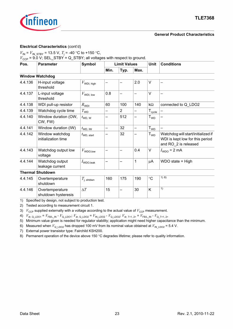
Window Watchdog4.4.136 H-input voltage
thresholdVWDI, high – – 2.0 V –
4.4.137 L-input voltage threshold
VWDI, low 0.8 – – V –
4.4.138 WDI pull-up resistor RWDI 60 100 140 kΩ connected to Q_LDO24.4.139 Watchdog cycle time TWD – 2 – Tcycle –4.4.140 Window duration (OW,
CW, FW)tWD, W – 512 – TWD –
4.4.141 Window duration (IW) tWD, IW – 32 – TWD –4.4.142 Window watchdog
initialization timetWD, start – 32 – TWD Watchdog will start/initialized if
WDI is kept low for this period and RO_2 is released
4.4.143 Watchdog output low voltage
VWDO,low – – 0.4 V IWDO = 2 mA
4.4.144 Watchdog output leakage current
IWDO,leak – – 1 µA WDO state = High
Thermal Shutdown4.4.145 Overtemperature
shutdownTj, shtdwn 160 175 190 °C 1) 8)
4.4.146 Overtemperature shutdown hysteresis
∆T 15 – 30 K 1)
1) Specified by design, not subject to production test.2) Tested according to measurement circuit 1.3) VCCP supplied externally with a voltage according to the actual value of VCCP measurement.4) Vdr, Q_LDO1 = VFB/L_IN - VQ_LDO1; Vdr, Q_LDO2 = VIN_LDO2 - VQ_LDO2; Vdr, T<1, 2> = VFB/L_IN - VQ_T<1, 2>
5) Minimum value given is needed for regulator stability; application might need higher capacitance than the minimum.6) Measured when VQ_LDO2 has dropped 100 mV from its nominal value obtained at VIN_LDO2 = 5.4 V.7) External power transistor type: Fairchild KSH200.8) Permanent operation of the device above 150 °C degrades lifetime; please refer to quality information.
Electrical Characteristics (cont’d)VIN = VIN_STBY = 13.5 V, Tj = -40 °C to +150 °C, VCCP = 9.0 V; SEL_STBY = Q_STBY; all voltages with respect to ground.Pos. Parameter Symbol Limit Values Unit Conditions
Min. Typ. Max.
Data Sheet 23 Rev. 2.1, 2010-11-22
TLE7368
Detailed Internal Circuits Description
5 Detailed Internal Circuits DescriptionIn the following the main circuit blocks of the TLE7368, namely the Buck converter, the linear regulators, thetrackers, the charge pump, the enable and reset circuits and the watchdog are described in more detail.
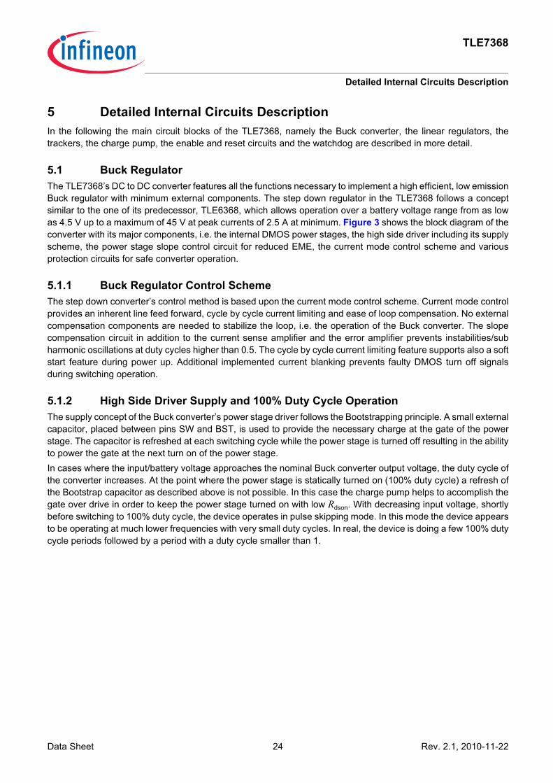
5.1 Buck RegulatorThe TLE7368’s DC to DC converter features all the functions necessary to implement a high efficient, low emissionBuck regulator with minimum external components. The step down regulator in the TLE7368 follows a conceptsimilar to the one of its predecessor, TLE6368, which allows operation over a battery voltage range from as lowas 4.5 V up to a maximum of 45 V at peak currents of 2.5 A at minimum. Figure 3 shows the block diagram of theconverter with its major components, i.e. the internal DMOS power stages, the high side driver including its supplyscheme, the power stage slope control circuit for reduced EME, the current mode control scheme and variousprotection circuits for safe converter operation.
5.1.1 Buck Regulator Control SchemeThe step down converter’s control method is based upon the current mode control scheme. Current mode controlprovides an inherent line feed forward, cycle by cycle current limiting and ease of loop compensation. No externalcompensation components are needed to stabilize the loop, i.e. the operation of the Buck converter. The slopecompensation circuit in addition to the current sense amplifier and the error amplifier prevents instabilities/subharmonic oscillations at duty cycles higher than 0.5. The cycle by cycle current limiting feature supports also a softstart feature during power up. Additional implemented current blanking prevents faulty DMOS turn off signalsduring switching operation.
5.1.2 High Side Driver Supply and 100% Duty Cycle OperationThe supply concept of the Buck converter’s power stage driver follows the Bootstrapping principle. A small externalcapacitor, placed between pins SW and BST, is used to provide the necessary charge at the gate of the powerstage. The capacitor is refreshed at each switching cycle while the power stage is turned off resulting in the abilityto power the gate at the next turn on of the power stage.In cases where the input/battery voltage approaches the nominal Buck converter output voltage, the duty cycle ofthe converter increases. At the point where the power stage is statically turned on (100% duty cycle) a refresh ofthe Bootstrap capacitor as described above is not possible. In this case the charge pump helps to accomplish thegate over drive in order to keep the power stage turned on with low Rdson. With decreasing input voltage, shortlybefore switching to 100% duty cycle, the device operates in pulse skipping mode. In this mode the device appearsto be operating at much lower frequencies with very small duty cycles. In real, the device is doing a few 100% dutycycle periods followed by a period with a duty cycle smaller than 1.
Data Sheet 24 Rev. 2.1, 2010-11-22

TLE7368
Detailed Internal Circuits Description
Figure 3 Buck Converter Block Diagram
5.1.3 Electromagnetic Emission ReductionThe Buck DMOS power stage is implemented as multiple cells. This allows to control the slope of the powerstage’s current at turn on/off by sequentially turning on/off the cells, achieving a smooth turn on/off and thereforeavoiding high frequency components in the electromagnetic emissions to the battery line. The current slope controlis adjusted internally, the typical current slew rate is 50 ns/A.
+ - + -
QS R
+ -
+ -
+ -
&
OTSD
Char
ge p
ump
Boot
stra
pch
arge
rBS
T
SW FB/L
_IN
CCP
C2-
C2+
C1-
C1+
IN
Erro
ram
plifi
er
Curre
ntco
mpa
rato
r
Over
tem
p.sh
utdo
wn
Oscil
lator
Slop
eco
mpe
nsat
ion
Curre
nt se
nse
ampl
ifier
Over
volta
gesh
utdo
wn
Leve
lsh
ifter
Leve
lsh
ifter
Slop
eco
ntro
l
Unde
r vol
tage
shut
down
High
side
drive
r
DMOS
pow
erst
ages
Data Sheet 25 Rev. 2.1, 2010-11-22

TLE7368
Detailed Internal Circuits Description
5.1.4 Charge PumpThe charge pump serves as support circuit for the Buck converter’s high side driver supply, the linear regulatorsdrive circuits for low drop operation and the internal device biasing blocks. In order to guarantee full deviceoperation at battery voltages as allow as even 4.5 V, the concept of a voltage tripler is chosen for the charge pump.It operates at a switching frequency of typical 2 MHz utilizing three small external capacitors, two pumping capsand one storage capacitor. The CCP circuit is equipped with a current limit function which avoids destruction incase of a short of one of the external CCP capacitors. The charge pump’s output, CCP, is designed to supply thecircuitry described above, it should not be used as e.g. driver rail for external on board/PCB circuits.
5.1.5 Buck Converter Protection CircuitsBesides the circuits mandatory for the Buck converter operation additional protection circuits are foreseen whichhelp preventing false operation of the device. Undervoltage lockouts are foreseen at the battery input line1) andthe high side driver supply rail to ensure the device operates only with proper voltages present. The overvoltageshutdown at the Buck converter output provides a safe high side shutdown for the case where the Buck controlloop becomes messed up due to non predictable circumstances. At overtemperatures the thermal shutdown circuitdisables the Buck converter until the device cools down to be enabled again.
5.2 Linear RegulatorsThe TLE7368 features three linear voltage regulator circuits, two fully integrated DMOS low drop voltageregulators and one integrated linear control circuit to operate with an external NPN power stage.Integrated linear regulator one (LDO1) offers a 5 V output and the second integrated linear regulator (LDO2) canbe configured with pin SEL_LDO2 either for 2.6 V or for 3.3 V. With SEL_LDO2 tied to GND 2.6 V will adjust atthe output of LDO2, SEL_LDO2 being connected to Q_LDO2 gives the 3.3 V option. The external regulator willadjust its output to 1.5 V or 1.2 V or 1.3 V (depending on variant of TLE7368) with the emitter of the NPN powerstage directly connected to pin FB_EXT, by using a voltage divider, higher output voltages can be achieved.The regulators are designed for low drop operation and offer high output voltage accuracies to meet the needs ofcurrent and next generation 32-bit microcontroller families. Additionally all regulators feature a short circuitprotection, i.e. the integrated regulators contain a output current limit function whereas the control circuit for theexternal NPN power stage limits the maximum base current.For low on chip power dissipation the input of LDO1 is internally directly connected to the Buck converter output(FB/L_IN). LDO2’s input is on purpose externally accessible at IN_LDO2. This allows the insertion of a dropelement between the Buck converter output and IN_LDO2 to split the power dissipation and avoid high losses onthe TLE7368. Similar for the external NPN power stage regulator, the collector of the NPN can be either connecteddirectly to the Buck converter output or a drop element can be inserted in between to split power dissipation.
5.3 Voltage Tracking RegulatorsFor off board/off PCB supplies, i.e. sensors, two voltage tracking regulators are incorporated in the TLE7368. Theiroutputs follow the output of the main 5 V regulator, Q_LDO1, within a tight tolerance of ±10 mV. The trackingregulators are implemented with bipolar PNP power stages for improved ripple rejection to reduce emission whenlead off board. Both tracker outputs can withstand short circuits to GND and battery in a range of -5 V to +40 V.When shorted to lower levels than the nominal output voltage level the current limit function prevents excessivecurrent draw.
1) Not shown in the schematic, Figure 3.
Data Sheet 26 Rev. 2.1, 2010-11-22

TLE7368
Detailed Internal Circuits Description
5.4 Power Up and Power Down SequencingIn a supply system with multiple outputs the sequence of enabling the individual regulators is important. Especially32-bit microcontrollers require a defined power up and power down sequencing. Figure 4 shows the details forthe power up and power down sequence of the TLE7368.At power up, the first circuit block to be enabled is the charge pump as it is mandatory for the other circuits tooperate. With the charge pump reaching its nominal value, the Buck converter starts to power up its output. Alsothe output voltage the linear regulators are enabled. The three linear regulators power up simultaneously. The 5 Vregulator acts as the master, the 3.3 V/2.6 V regulator and the 1.5 V regulator follow. As the 5 V regulator powersup also the tracking regulators follow. The ramp if the increasing output voltage of each line is determined by theconnected output capacitance, the load current and the current limit of the regulator under consideration. Inaddition an integrated supervision circuit ensures the following two conditions during power-up:
-0.3 V < (VQ_LDO1 - VQ_LDO2) < 3.1 V and (1)
-0.3 V < (VQ_LDO2 - VFB_EXT) (2)
The power down sequence is practically vice versa to the start up procedure. With the battery decreasing to zerothe charge pump and Buck regulator will stop to operate at the minimum battery threshold, the Buck output voltagewill fall down and so will the outputs of the linear regulators.In the event where the device is disabled, EN_IGN = low and EN_uC = low, the charge pump, the Buck converterand the linear regulators are disabled immediately.The linear regulators’ outputs are not discharged actively in any case of power down. Diode circuitry (i.e. Schottkydiodes) might be necessary to avoid violation of certain microcontrollers’ sequencing requirements.
Data Sheet 27 Rev. 2.1, 2010-11-22

TLE7368
Detailed Internal Circuits Description
Figure 4 Power Sequencing of the TLE7368
VIN
VIN, on
VCCP
VCCP, ok
VBST
VSW
VBST, on
VFB/L_IN
VQ_LDO1
VQ_LDO2
VFB_EXT
VQ_T<1,2>
VQ_LDO1
VQ_LDO2
VQ_LDO1
-0.3 < (Q_LDO1-Q_LDO2) < 3.1V
-0.3 < ( Q_LDO2 - FB_EXT)
VIN, off
*)
*)
*)
*)
*)
Linear regulators not activelydischarged at power down; externaSchottky diodes required to meetuC”s sequencing requirements
*) drop depending onapplication / setup
t
t
t
t
t
t
t
t
t
Data Sheet 28 Rev. 2.1, 2010-11-22

TLE7368
Detailed Internal Circuits Description
5.5 Stand-by RegulatorThe intention of the stand-by or keep alive regulator is to supply e.g. external memory even with the mainmicrocontroller supply being disabled. Therefore the state of the stand-by regulator is not controlled by the enableblock, but it is active all the time. The stand-by regulator starts to operate as soon as the battery voltage increasesabove its operating threshold. The current consumption during single operation of the stand-by regulator isreduced to a minimum. It can be configured for output voltages as either 1.0 V or 2.6 V through the SEL_STBY pin.
5.6 Overtemperature ProtectionAt junction temperatures between 160 °C and 190 °C, which can be caused by e.g. excessive power dissipationor increased ambient temperatures, the overtemperature protection kicks in and disables the Buck converter. Withthe Buck converter disabled the linear regulators will most likely not be able to keep up their output voltage and asystem reset can be expected. Due to the drop in power dissipation the junction temperature will decrease. Thebuilt in hysteresis circuit ensures that the junction temperature cools down by a certain temperature delta beforethe Buck converter is enabled again.
5.7 Device Enable FunctionThe device enable block controls the operation of the Buck converter as well as of the linear regulators and trackerblocks. Two external signal inputs determine the state of those blocks, a high voltage input EN_IGN and a lowvoltage input EN_uC. Internally the two signals are logic OR-ed which means that with either signal the Buck andlinear regulators can be turned on or held active, provided that the battery voltage is above its minimum operatingrange. In order to turn off the regulator blocks, the signals on both inputs, EN_IGN and EN_uC must be lower thantheir deactivating threshold. The stand-by regulator’s operation is not affected by the device enable block.
5.8 Reset FunctionThe Reset concept of the TLE7368 is chosen to support multiple microcontroller platforms. Two open drainoutputs, i.e. the Reset outputs, RO_1 and RO_2, indicate the states of the different regulators. Figure 5 gives thedetails on the Reset timing. RO_1 is tied to LDO1 and will indicate whenever its output, Q_LDO1, is crossing theunder- or overvoltage threshold. The second Reset output, RO_2, turns low whenever one of the two outputs,Q_LDO2 or FB_EXT, are crossing their under- and overvoltage thresholds. At power up in order to avoid a faultymicrocontroller start, a so called Reset delay function, i.e. the Reset release delay, is implemented. This delay untilthe reset is released, counted from the time where the regulator outputs cross the threshold, is determined by asmall external delay capacitor at pin RT.The power up reset delay time tRD is directly proportional to the capacitance CRT within the capacitance range of0.33 nF … 4.7 nF:
tRD = 160 × 50 µs × CRT/nF (3)
For the tolerance calculation please refer to the parameters 4.4.81, 4.4.82 and 4.4.83. In order to find the worstcase limits of tRD the capacitance tolerance should be taken into account.The Reset generators within the TLE7368 are supplied from multiple sources, VIN_STBY, VCCP, VFB_L/IN,VQ_LDO1 and VQ_LDO2, to fulfill next generation microcontroller requirements during power up and power down.
Data Sheet 29 Rev. 2.1, 2010-11-22

TLE7368
Detailed Internal Circuits Description
Figure 5 Reset Timing TLE7368
VFB/L_IN
VQ_LDO1
VQ_LDO2
VFB_EXT
VRO_2**)
t
t
t
t
VRO_1*)
t
tRD, RO_1tRD, RO_1
tUVRR, RO_1
< tUVRR, RO_1
tUVRR, RO_1
VORT Q_LDO1, in
tRD, RO_1
VORT Q_LDO1, deVURT Q_LDO1, in
VURT Q_LDO1, de
VORT Q_LDO2, in
VORT Q_LDO2, deVURT Q_LDO2, in
VURT Q_LDO2, de
VURT FB_EXT, in
VURT FB_EXT, de
VORT FB_EXT, in
VORT FB_EXT, de
tRD, RO_2
tUVRR, RO_2
tRD, RO_2
< tUVRR, RO_2
< tOVRR, RO_1
tOVRR, RO_2
tRD, RO_2
tOVRR, RO_2
tRD, RO_2
< tOVRR, RO_2 < tUVRR, RO_2
< tOVRR, RO_2
tUVRR, RO_2
*) pulled to e.g. Q_LDO1 by 10kOhm **) pulled to e.g. Q_LDO2 by 10kOhm
Data Sheet 30 Rev. 2.1, 2010-11-22

TLE7368
Detailed Internal Circuits Description
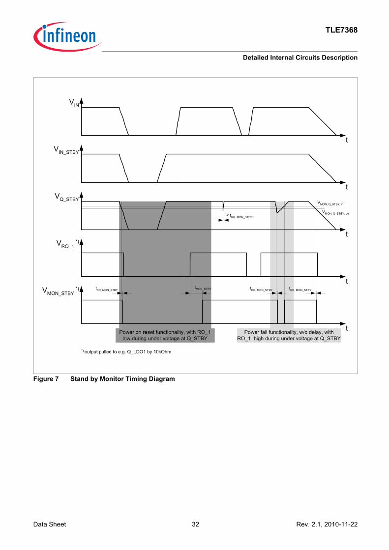
5.9 Monitoring CircuitThe monitoring block within the TLE7368 detects an undervoltage at the stand-by regulator output and is able todistinguish between two different undervoltage situations. When the stand-by output gets back into regulation afteran undervoltage event, the timing on the MON_STBY output signal indicates the kind of undervoltage scenariowhich has happened before. The behavior of the monitoring block is also described in Figure 6 and Figure 7below.In case of an undervoltage at the stand-by regulator with the 5 V regulator LDO1 in regulation (which means thatRO_1 = HIGH) the monitoring circuit has basically a power fail functionality which means that the MON_STBYoutput will be LOW just as long as the undervoltage at the stand-by output occurs. As soon as Q_STBY is comingback into regulation MON_STBY turns high again.When the 5 V regulator is out of regulation (RO_1 = LOW), e.g. in case of EN_uC = EN_IGN = LOW, theMON_STBY will turn LOW again if an undervoltage event happens at Q_STBY. The difference to the scenariodescribed above is now that when Q_STBY gets back into regulation the toggling of the MON_STBY output toHIGH is coupled with the 5 V Reset line, RO_1, turning HIGH. In detail, the MON_STBY line turns high delayedby tMON_STBY after the Reset line RO_1 had gone high.
Figure 6 Stand by Monitor State Diagram
MON = HighVQ_STBY < VMON, Q_STBY, de
andRO_1 = High Monitor timing
= don’t care
MON = Low
Monitor timing= no delay *)
MON = Low
Monitor timing= delay**)
*) power fail functionionality
**) power on reset functionality
VQ_STBY > VMON, Q_STBY, inand
RO_1 = High
VQ_STBY < VMON, Q_STBY, deand
RO_1 = Low
VQ_STBY > VMON, Q_STBY, inand
RO_1 = High
VQ_STBY < VMON, Q_STBY, deand
RO_1 = Low
VQ_STBY > VMON, Q_STBY, inand
RO_1 = Low
Data Sheet 31 Rev. 2.1, 2010-11-22
TLE7368
Detailed Internal Circuits Description
Figure 7 Stand by Monitor Timing Diagram
Power on reset functionality, with RO_1low during under voltage at Q_STBY
VIN_STBY
t
*) output pulled to e.g. Q_LDO1 by 10kOhm
VRO_1 *)
tVMON_STBY
*)
t
VQ_STBY
t
tMON_STBY
< tRR, MON_STBY1
VMON, Q_STBY, in
VMON, Q_STBY, de
tRR, MON_STBY tRR, MON_STBY tRR, MON_STBY
Power fail functionality, w/o delay, withRO_1 high during under voltage at Q_STBY
VIN
t
Data Sheet 32 Rev. 2.1, 2010-11-22

TLE7368
Detailed Internal Circuits Description
5.10 Watchdog Circuit
Figure 8 Window Watchdog State Diagram
Principle of Operation:A Window Watchdog is integrated in the TLE7368 to monitor a microcontroller. The Window Watchdog duty cycleconsists of an "Open window" and a "Closed window". The microcontroller that is being monitored has to send aperiodic falling edge trigger signal to the watchdog input pin WDI within the "Open Window". If a trigger signal isnot sent or if it is sent during the "Closed Window", then Watchdog Output (WDO) switches from high to lowsignaling a potential microcontroller fault has occurred. The watchdog cycle time TWD is derived from the time baseTCycle. An external capacitor connected between pins RT and GND determines TCycle.
Initialization:The Watchdog is switched off per default and activated by pulling WDI to low at least for the time tWD,start after RO_2has turned to high. Watchdog input pin WDI has an integrated pull-up resistor RWDI connected to Q_LDO2. If WDItransitions to high before tWD,start has elapsed, then the watchdog will not start operation. To initialize the Watchdogthe watchdog input WDI should transition to high within the "Ignore Window". The WDI signal may also transitionto high during the following "Open Window", but sufficient time must be left for a falling edge transition before theend of the "Open Window". The watchdog function is turned off following a RO_2 reset, and must be reinitializedto be turned back on.
Normal Operation:Please refer to Figure 8.The Watchdog starts operating in the "Ignore Window" state for a duration of tWD,IW. Within the "Ignore Window"the microcontroller is given time to initialize. Any signal to watchdog input WDI within the "Ignore Window" isignored. After time tWD,IW, the watchdog transitions from the "Ignore Window" state to the "Open Window" state fora maximum duration of tWD,W. Within the "Open Window" a valid trigger signal must be applied to the watchdog
AEA03533.VSD
No Trigger
ClosedWindow
OpenWindow
Trigger
WDO = LOW IgnoreWindow
Always
AlwaysNo Trigger DuringOpen Window
Trigger DuringClosed Window
Data Sheet 33 Rev. 2.1, 2010-11-22
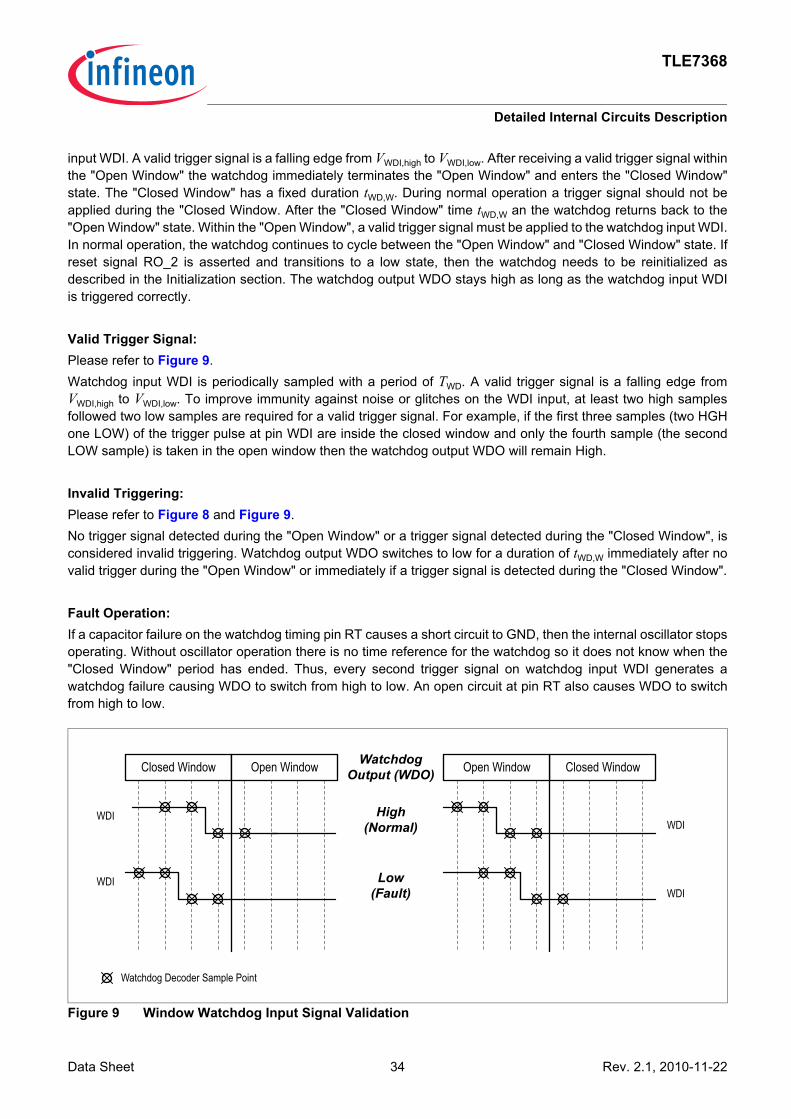
TLE7368
Detailed Internal Circuits Description
input WDI. A valid trigger signal is a falling edge from VWDI,high to VWDI,low. After receiving a valid trigger signal withinthe "Open Window" the watchdog immediately terminates the "Open Window" and enters the "Closed Window"state. The "Closed Window" has a fixed duration tWD,W. During normal operation a trigger signal should not beapplied during the "Closed Window. After the "Closed Window" time tWD,W an the watchdog returns back to the"Open Window" state. Within the "Open Window", a valid trigger signal must be applied to the watchdog input WDI.In normal operation, the watchdog continues to cycle between the "Open Window" and "Closed Window" state. Ifreset signal RO_2 is asserted and transitions to a low state, then the watchdog needs to be reinitialized asdescribed in the Initialization section. The watchdog output WDO stays high as long as the watchdog input WDIis triggered correctly.
Valid Trigger Signal:Please refer to Figure 9.Watchdog input WDI is periodically sampled with a period of TWD. A valid trigger signal is a falling edge fromVWDI,high to VWDI,low. To improve immunity against noise or glitches on the WDI input, at least two high samplesfollowed two low samples are required for a valid trigger signal. For example, if the first three samples (two HGHone LOW) of the trigger pulse at pin WDI are inside the closed window and only the fourth sample (the secondLOW sample) is taken in the open window then the watchdog output WDO will remain High.
Invalid Triggering:Please refer to Figure 8 and Figure 9.No trigger signal detected during the "Open Window" or a trigger signal detected during the "Closed Window", isconsidered invalid triggering. Watchdog output WDO switches to low for a duration of tWD,W immediately after novalid trigger during the "Open Window" or immediately if a trigger signal is detected during the "Closed Window".
Fault Operation:If a capacitor failure on the watchdog timing pin RT causes a short circuit to GND, then the internal oscillator stopsoperating. Without oscillator operation there is no time reference for the watchdog so it does not know when the"Closed Window" period has ended. Thus, every second trigger signal on watchdog input WDI generates awatchdog failure causing WDO to switch from high to low. An open circuit at pin RT also causes WDO to switchfrom high to low.
Figure 9 Window Watchdog Input Signal Validation
Data Sheet 34 Rev. 2.1, 2010-11-22
TLE7368
Application Information
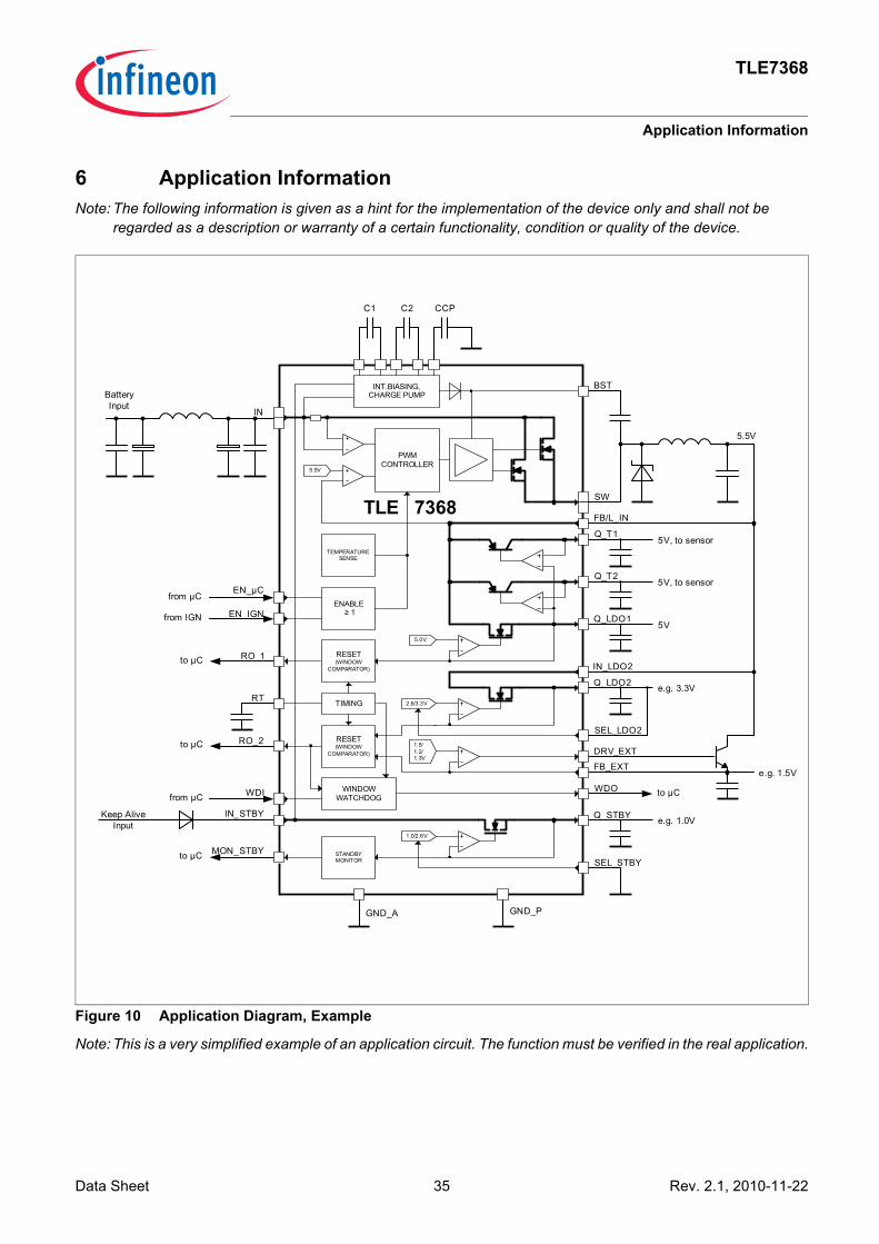
6 Application InformationNote: The following information is given as a hint for the implementation of the device only and shall not be
regarded as a description or warranty of a certain functionality, condition or quality of the device.
Figure 10 Application Diagram, Example
Note: This is a very simplified example of an application circuit. The function must be verified in the real application.
5.5V
5.0V
2.6/3.3V
1.5/ 1.2/ 1.3V
1.0/2.6V
BST
SW
FB/L_IN
Q_T1
Q_T2
Q_LDO1
IN_LDO2
Q_LDO2
SEL_LDO2
DRV_EXT
FB_EXT
WDO
Q_STBY
SEL_STBY
GND_A
MON_STBY
IN_STBY
WDI
RO_2
RT
RO_1
EN_µC
EN_IGN
IN
C2 CCPC1
GND_P
INT.BIASING,CHARGE PUMP
PWMCONTROLLER
ENABLE ≥ 1
RESET(WINDOW
COMPARATOR)
RESET(WINDOW
COMPARATOR)
STANDBYMONITOR
WINDOWWATCHDOG
TEMPERATURESENSE
TLE 7368
TIMING
5V, to sensor
5V, to sensor
5V
e.g. 3.3V
e.g. 1.0V
e.g. 1.5V
to µC
to µC
from µC
to µC
to µC
from µC
from IGN
Keep Alive Input
Battery Input
5.5V
Data Sheet 35 Rev. 2.1, 2010-11-22
TLE7368
Application Information
This section intends to give hints for correct set up of the IC, i.e. to avoid misbehavior caused by the influence ofother PCB board circuits and shows also how to calculate external components, power loss, etc.
6.1 Choosing Components for the Buck RegulatorStable operation of the Buck converter is ensured when choosing the external passive components according tothe characteristics given below:• Buck inductance: 18 µH < LBuck < 220 µH• Buck output capacitor: CBuck > 20 µF• ESR of Buck output capacitor: ESR_CBuck < 150 mΩ
6.2 Setting up LDO1, LDO2The linear regulators LDO1 and LDO2 need to be connected to appropriate output capacitors in order to keep theregulation loop stable and avoid oscillations. The essential parameters of the output capacitor are the minimumcapacitance and the equivalent series resistance (ESR). The required ranges for each output are specified inChapter 4.4 (Electrical Characteristics). Tantalum capacitors as well as multi layer ceramic capacitors aresuitable for LDO1 and LDO2.
6.3 Setting up of LDO3LDO3 consists of an integrated regulator which needs to be equipped with an external power transistor (NPN-Type). Suitable NPN power transistors types are e.g. KSH 200 from Fairchild semiconductor or NJD 2873T4 fromON semiconductor. The most important parameters to be checked when choosing the external transistor are the‘current gain bandwidth product’ (fT), the ‘DC current gain’ (hFE) and the thermal resistance of the package.Darlington type transistors should not be used. For stability of the regulation loop a multi layer ceramic capacitorof min. 4.7 µF must be connected to the LDO3 output voltage (Emitter of the external power transistor). In orderto improve suppression load current steps an additional capacitor of tantalum type can be connected in parallel.In case LDO3 voltage is not needed the external NPN transistor can be spared. For this configuration the pins‘DRV_EXT’ and ‘FB_EXT’ should be directly connected to each other in order to ensure correct operation ofReset 2. Also in this case a small ceramic capacitor of 220 nF connected from pin ‘FB_EXT’ to GND isrecommended in order to avoid oscillations of the regulation loop LDO3.
Table 1 LDO2 Output Voltage ConfigurationNo. SEL_LDO2 Q_LDO21 GND 2.6 V2 Q_LDO2 3.3 V
Data Sheet 36 Rev. 2.1, 2010-11-22
TLE7368
Application Information
6.4 Setting up the Stand-by RegulatorThe stand by regulator provides an output current up to 30 mA sourced via linear regulation directly from Batteryeven when the main regulator is disabled. This low quiescent current regulator is commonly used as supply forstand by memory. The output voltage can be selected as 1.0 V or 2.6 V. For stability of the regulation loop theoutput Q_STBY should be connected via a ceramic capacitor (470 nF to 2 µF) to GND.
6.4.1 Stand-by Regulator’s Output Voltage ConfigurationThe stand by regulator provides an output voltage of nominal 1.0 V or 2.6 V which is associated with anappropriate stand-by monitoring threshold. The output voltage level is selected by the SEL_STBY configuration.Connecting SEL_STBY to GND results in a voltage level of 2.6 V at Q_STBY, while connecting SEL_STBY withQ_STBY leads to 1.0 V configuration. An integrated pull-up current ensures that the system will turn in the lowerstand-by voltage mode in case of open mode at the SEL_STBY pin. However the SEL_STBY pin should beconnected either to Q_STBY or to GND in order to select the appropriate Q_STBY voltage level. Intermediatevoltage levels at SEL_STBY should be avoided.
Table 2 Stand-by Regulator’s Output Voltage ConfigurationNo. SEL_STBY Q_STBY1 GND 2.6 V2 Q_STBY 1.0 V
Data Sheet 37 Rev. 2.1, 2010-11-22
TLE7368
Package Outlines
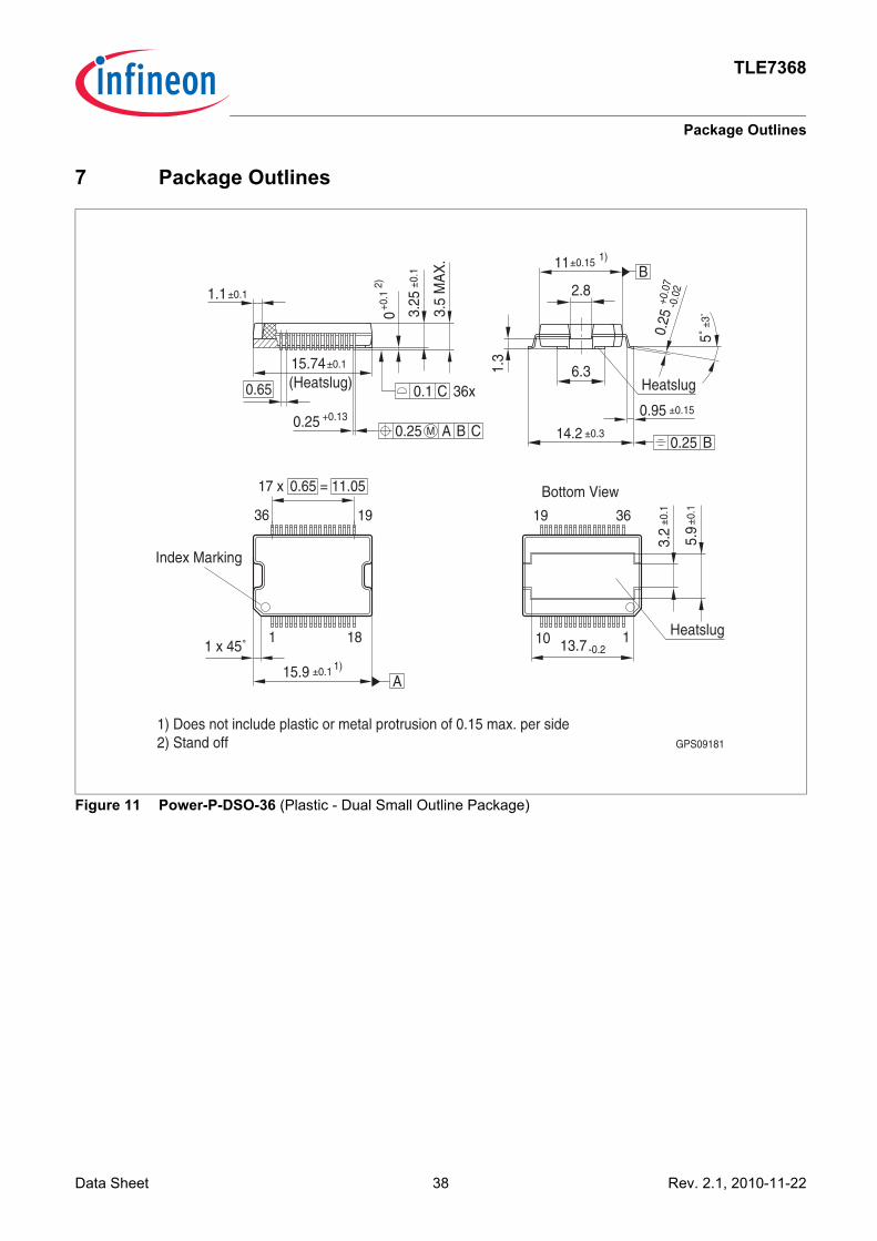
7 Package Outlines
Figure 11 Power-P-DSO-36 (Plastic - Dual Small Outline Package)
Bottom View
1) Does not include plastic or metal protrusion of 0.15 max. per side2) Stand off
1 18
0.25
±0.1
GPS09181
1.1
36
+0.130.25
36x
19
M
(Heatslug)15.74
0.65
17 x 0.65 = 11.05
±0.1
CA B
19
C3.
25
3.5
MA
X.
+0.1
2)0
0.1±0
.1
36
2.8B
11±0.15 1)
1.3
5˚0.25 ±3
˚
-0.0
2+0
.07
6.3
14.2 ±0.3B
±0.15
0.25
Heatslug
0.95
Heatslug
±0.1
5.9
3.2
±0.1
13.710 1-0.2
Index Marking
15.9 1)±0.1A
1 x 45˚
Data Sheet 38 Rev. 2.1, 2010-11-22

TLE7368
Package Outlines
Figure 12 PG-DSO-36 (Plastic Green - Dual Small Outline Package)
Green Product (RoHS compliant)To meet the world-wide customer requirements for environmentally friendly products and to be compliant withgovernment regulations the device is available as a green product. Green products are RoHS-Compliant (i.ePb-free finish on leads and suitable for Pb-free soldering according to IPC/JEDEC J-STD-020).
For additional package information, please go to the Infineon InternetPage “Products”: http://www.infineon.com/products. Dimensions in mm
PG-DSO-36-24, -38, -41, -42, -50-PO V09
Exposed Diepad
Index Marking
1) Does not include plastic or metal protrusion of 0.15 max. per side2) Does not include dambar protrusion of 0.05 max. per side3) Distance from leads bottom (= seating plane) to exposed diepad
Index Marking
1 18
36 19
18 1
19 36
Bottom View
0.65
17 x 0.65 = 11.05
±0.080.33 2)
3)
A-B0.17 M 36xC
C C
D
0.1 36xSEATING PLANE
0...0
.10
STA
ND
OFF
-0.2
2.45
2.55
MA
X.
1.1
-0.27.6 1)
0.35 x 45˚
0.7 ±0.2
10.3±0.3
+0.0
90.
23
8˚ M
AX
.
A
D
1)12.8 -0.2
B
PG-DSO-36-38PG-DSO-36-38PG-DSO-36-24, -41, -42Package
A6901-C007A6901-C003A6901-C001Leadframe
5.277
4.6PG-DSO-36-50 A6901-C008 6.0 5.4
5.15.1
Exposed Diepad Dimensions
Ejector Mark
4)
4) Excluding the mold flash allowance of 0.3 max per side
Ex
Ex Ey
Ey
Data Sheet 39 Rev. 2.1, 2010-11-22
Data Sheet 40 Rev. 2.1, 2010-11-22
TLE7368
Revision History
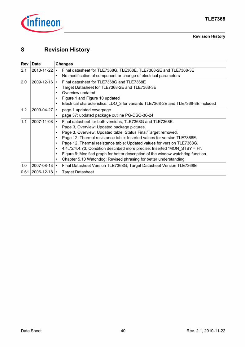
8 Revision History
Rev Date Changes2.1 2010-11-22 • Final datasheet for TLE7368G, TLE368E, TLE7368-2E and TLE7368-3E
• No modification of component or change of electrical parameters2.0 2009-12-16 • Final datasheet for TLE7368G and TLE7368E
• Target Datasheet for TLE7368-2E and TLE7368-3E• Overview updated• Figure 1 and Figure 10 updated• Electrical characteristics: LDO_3 for variants TLE7368-2E and TLE7368-3E included
1.2 2009-04-27 • page 1 updated coverpage• page 37: updated package outline PG-DSO-36-24
1.1 2007-11-08 • Final datasheet for both versions, TLE7368G and TLE7368E.• Page 3, Overview: Updated package pictures.• Page 3, Overview: Updated table: Status Final/Target removed.• Page 12, Thermal resistance table: Inserted values for version TLE7368E.• Page 12, Thermal resistance table: Updated values for version TLE7368G.• 4.4.72/4.4.73: Condition described more precise: Inserted “MON_STBY = H”.• Figure 9: Modified graph for better description of the window watchdog function.• Chapter 5.10 Watchdog: Revised phrasing for better understanding
1.0 2007-08-13 • Final Datasheet Version TLE7368G; Target Datasheet Version TLE7368E0.61 2006-12-18 • Target Datasheet

Edition 2010-11-22Published byInfineon Technologies AG81726 Munich, Germany© 2010 Infineon Technologies AGAll Rights Reserved.
Legal DisclaimerThe information given in this document shall in no event be regarded as a guarantee of conditions or characteristics. With respect to any examples or hints given herein, any typical values stated herein and/or any information regarding the application of the device, Infineon Technologies hereby disclaims any and all warranties and liabilities of any kind, including without limitation, warranties of non-infringement of intellectual property rights of any third party.
InformationFor further information on technology, delivery terms and conditions and prices, please contact the nearest Infineon Technologies Office (www.infineon.com).
WarningsDue to technical requirements, components may contain dangerous substances. For information on the types in question, please contact the nearest Infineon Technologies Office.Infineon Technologies components may be used in life-support devices or systems only with the express written approval of Infineon Technologies, if a failure of such components can reasonably be expected to cause the failure of that life-support device or system or to affect the safety or effectiveness of that device or system. Life support devices or systems are intended to be implanted in the human body or to support and/or maintain and sustain and/or protect human life. If they fail, it is reasonable to assume that the health of the user or other persons may be endangered.