TL494 Pulse-Width-Modulation Control · PDF fileTL494 Pulse-Width-Modulation Control Circuits...
21
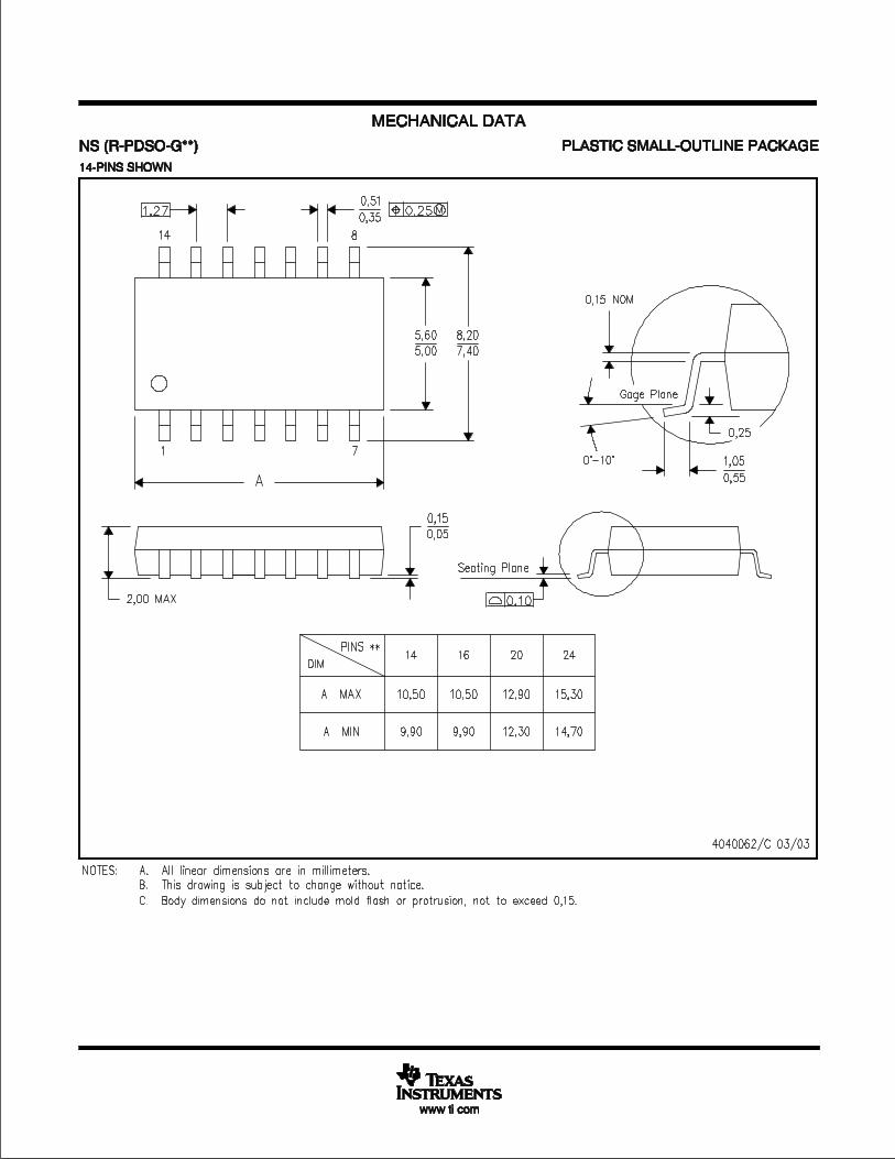
1 2 3 4 5 6 7 8 16 15 14 13 12 11 10 9 1IN+ 1IN- FEEDBACK DTC CT RT GND C1 2IN+ 2IN- REF OUTPUT CTRL V CC C2 E2 E1 D, DB, N, NS, OR PW PACKAGE (TOP VIEW) TL494 www.ti.com SLVS074F – JANUARY 1983 – REVISED JANUARY 2014 TL494 Pulse-Width-Modulation Control Circuits Check for Samples: TL494 1FEATURES DESCRIPTION The TL494 device incorporates all the functions • Complete PWM Power-Control Circuitry required in the construction of a pulse-width- • Uncommitted Outputs for 200-mA Sink or modulation (PWM) control circuit on a single chip. Source Current Designed primarily for power-supply control, this • Output Control Selects Single-Ended or device offers the flexibility to tailor the power-supply control circuitry to a specific application. Push-Pull Operation • Internal Circuitry Prohibits Double Pulse at The TL494 device contains two error amplifiers, an Either Output on-chip adjustable oscillator, a dead-time control (DTC) comparator, a pulse-steering control flip-flop, a • Variable Dead Time Provides Control Over 5-V, 5%-precision regulator, and output-control Total Range circuits. • Internal Regulator Provides a Stable 5-V The error amplifiers exhibit a common-mode voltage Reference Supply With 5% Tolerance range from –0.3 V to V CC – 2 V. The dead-time • Circuit Architecture Allows Easy control comparator has a fixed offset that provides Synchronization approximately 5% dead time. The on-chip oscillator can be bypassed by terminating RT to the reference output and providing a sawtooth input to CT, or it can drive the common circuits in synchronous multiple-rail power supplies. The uncommitted output transistors provide either common-emitter or emitter-follower output capability. The TL494 device provides for push-pull or single- ended output operation, which can be selected through the output-control function. The architecture of this device prohibits the possibility of either output being pulsed twice during push-pull operation. The TL494C device is characterized for operation from 0°C to 70°C. The TL494I device is characterized for operation from –40°C to 85°C. 1 Please be aware that an important notice concerning availability, standard warranty, and use in critical applications of Texas Instruments semiconductor products and disclaimers thereto appears at the end of this data sheet. PRODUCTION DATA information is current as of publication date. Copyright © 1983–2014, Texas Instruments Incorporated Products conform to specifications per the terms of the Texas Instruments standard warranty. Production processing does not necessarily include testing of all parameters.
-
Upload
duongkhanh -
Category
Documents
-
view
232 -
download
3
Transcript of TL494 Pulse-Width-Modulation Control · PDF fileTL494 Pulse-Width-Modulation Control Circuits...
1
2
3
4
5
6
7
8
16
15
14
13
12
11
10
9
1IN+1IN−
FEEDBACKDTC
CTRT
GNDC1
2IN+2IN−REFOUTPUT CTRLVCC
C2E2E1
D, DB, N, NS, OR PW PACKAGE(TOP VIEW)
TL494www.ti.com SLVS074F –JANUARY 1983–REVISED JANUARY 2014
TL494 Pulse-Width-Modulation Control CircuitsCheck for Samples: TL494
1FEATURES DESCRIPTIONThe TL494 device incorporates all the functions• Complete PWM Power-Control Circuitryrequired in the construction of a pulse-width-• Uncommitted Outputs for 200-mA Sink or modulation (PWM) control circuit on a single chip.
Source Current Designed primarily for power-supply control, this• Output Control Selects Single-Ended or device offers the flexibility to tailor the power-supply
control circuitry to a specific application.Push-Pull Operation• Internal Circuitry Prohibits Double Pulse at The TL494 device contains two error amplifiers, an
Either Output on-chip adjustable oscillator, a dead-time control(DTC) comparator, a pulse-steering control flip-flop, a• Variable Dead Time Provides Control Over5-V, 5%-precision regulator, and output-controlTotal Rangecircuits.• Internal Regulator Provides a Stable 5-VThe error amplifiers exhibit a common-mode voltageReference Supply With 5% Tolerancerange from –0.3 V to VCC – 2 V. The dead-time• Circuit Architecture Allows Easy control comparator has a fixed offset that providesSynchronization approximately 5% dead time. The on-chip oscillatorcan be bypassed by terminating RT to the referenceoutput and providing a sawtooth input to CT, or it candrive the common circuits in synchronous multiple-railpower supplies.
The uncommitted output transistors provide eithercommon-emitter or emitter-follower output capability.The TL494 device provides for push-pull or single-ended output operation, which can be selectedthrough the output-control function. The architectureof this device prohibits the possibility of either outputbeing pulsed twice during push-pull operation.
The TL494C device is characterized for operationfrom 0°C to 70°C. The TL494I device is characterizedfor operation from –40°C to 85°C.
1
Please be aware that an important notice concerning availability, standard warranty, and use in critical applications ofTexas Instruments semiconductor products and disclaimers thereto appears at the end of this data sheet.
PRODUCTION DATA information is current as of publication date. Copyright © 1983–2014, Texas Instruments IncorporatedProducts conform to specifications per the terms of the TexasInstruments standard warranty. Production processing does notnecessarily include testing of all parameters.
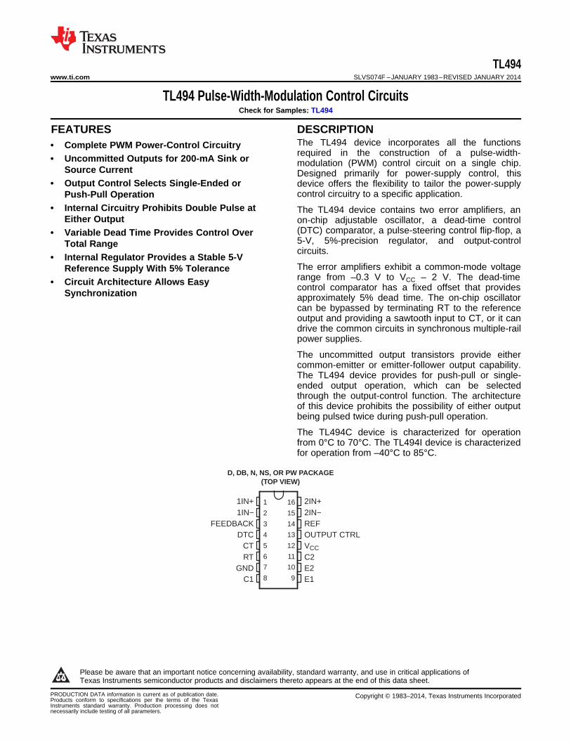
GND
VCC
ReferenceRegulator
C1
Pulse-SteeringFlip-Flop
C1
1D
DTC
CTRT
PWMComparator
+
−
Error Amplifier 1
≈ 0.1 V
Dead-Time ControlComparator
Oscillator
OUTPUT CTRL(see Function T able)
0.7 mA
E1
C2
E2
+
−
Error Amplifier 2
1IN+
1IN−
2IN+
2IN−
FEEDBACK
REF
65
4
1
2
16
15
3
13
8
9
11
10
12
14
7
Q1
Q2≈ 0.7 V
TL494SLVS074F –JANUARY 1983–REVISED JANUARY 2014 www.ti.com
This integrated circuit can be damaged by ESD. Texas Instruments recommends that all integrated circuits be handled withappropriate precautions. Failure to observe proper handling and installation procedures can cause damage.
ESD damage can range from subtle performance degradation to complete device failure. Precision integrated circuits may be moresusceptible to damage because very small parametric changes could cause the device not to meet its published specifications.
Function TableINPUT TO OUTPUT FUNCTIONOUTPUT CTRLVI = GND Single-ended or parallel outputVI = Vref Normal push-pull operation
Functional Block Diagram
2 Submit Documentation Feedback Copyright © 1983–2014, Texas Instruments Incorporated
Product Folder Links :TL494
TL494www.ti.com SLVS074F –JANUARY 1983–REVISED JANUARY 2014
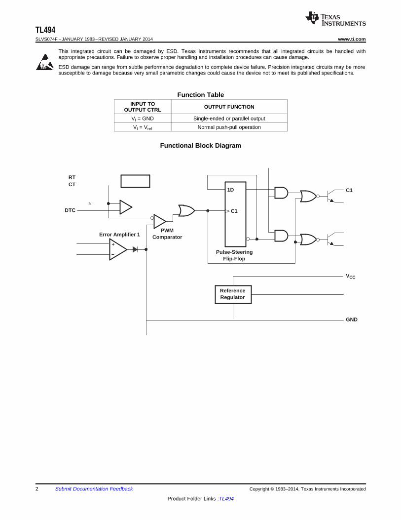
Absolute Maximum Ratingsover operating free-air temperature range (unless otherwise noted) (1)
MIN MAX UNITVCC Supply voltage (2) 41 VVI Amplifier input voltage VCC + 0.3 VVO Collector output voltage 41 VIO Collector output current 250 mA
D package 73DB package 82
θJA Package thermal impedance (3) (4) N package 67 °C/WNS package 64PW package 108
Lead temperature 1,6 mm (1/16 inch) from case for 10 seconds 260 °CTstg Storage temperature range –65 150 °C
(1) Stresses beyond those listed under Absolute Maximum Ratings may cause permanent damage to the device. These are stress ratingsonly, and functional operation of the device at these or any other conditions beyond those indicated under Recommended OperatingConditions is not implied. Exposure to absolute-maximum-rated conditions for extended periods may affect device reliability.
(2) All voltages are with respect to the network ground terminal.(3) Maximum power dissipation is a function of TJ(max), θJA, and TA. The maximum allowable power dissipation at any allowable ambient
temperature is PD = (TJ(max) – TA)/θJA. Operating at the absolute maximum TJ of 150°C can affect reliability.(4) The package thermal impedance is calculated in accordance with JESD 51-7.
Recommended Operating ConditionsMIN MAX UNIT
VCC Supply voltage 7 40 VVI Amplifier input voltage –0.3 VCC – 2 VVO Collector output voltage 40 V
Collector output current (each transistor) 200 mACurrent into feedback terminal 0.3 mA
fOSC Oscillator frequency 1 300 kHzCT Timing capacitor 0.47 10000 nFRT Timing resistor 1.8 500 kΩ
TL494C 0 70TA Operating free-air temperature °C
TL494I –40 85
Copyright © 1983–2014, Texas Instruments Incorporated Submit Documentation Feedback 3
Product Folder Links :TL494
N
n1
(xn X)2
N 1
TL494SLVS074F –JANUARY 1983–REVISED JANUARY 2014 www.ti.com
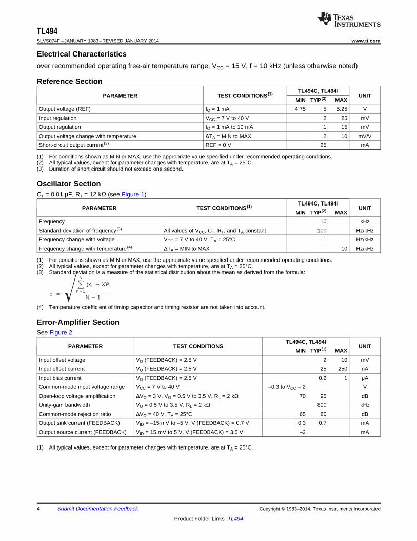
Electrical Characteristicsover recommended operating free-air temperature range, VCC = 15 V, f = 10 kHz (unless otherwise noted)
Reference SectionTL494C, TL494I
PARAMETER TEST CONDITIONS (1) UNITMIN TYP (2) MAX
Output voltage (REF) IO = 1 mA 4.75 5 5.25 VInput regulation VCC = 7 V to 40 V 2 25 mVOutput regulation IO = 1 mA to 10 mA 1 15 mVOutput voltage change with temperature ΔTA = MIN to MAX 2 10 mV/VShort-circuit output current (3) REF = 0 V 25 mA
(1) For conditions shown as MIN or MAX, use the appropriate value specified under recommended operating conditions.(2) All typical values, except for parameter changes with temperature, are at TA = 25°C.(3) Duration of short circuit should not exceed one second.
Oscillator SectionCT = 0.01 μF, RT = 12 kΩ (see Figure 1)
TL494C, TL494IPARAMETER TEST CONDITIONS (1) UNIT
MIN TYP (2) MAXFrequency 10 kHzStandard deviation of frequency (3) All values of VCC, CT, RT, and TA constant 100 Hz/kHzFrequency change with voltage VCC = 7 V to 40 V, TA = 25°C 1 Hz/kHzFrequency change with temperature (4) ΔTA = MIN to MAX 10 Hz/kHz
(1) For conditions shown as MIN or MAX, use the appropriate value specified under recommended operating conditions.(2) All typical values, except for parameter changes with temperature, are at TA = 25°C.(3) Standard deviation is a measure of the statistical distribution about the mean as derived from the formula:
(4) Temperature coefficient of timing capacitor and timing resistor are not taken into account.
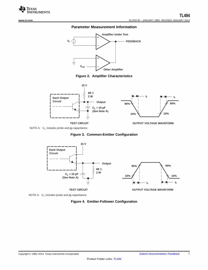
Error-Amplifier SectionSee Figure 2
TL494C, TL494IPARAMETER TEST CONDITIONS UNIT
MIN TYP (1) MAXInput offset voltage VO (FEEDBACK) = 2.5 V 2 10 mVInput offset current VO (FEEDBACK) = 2.5 V 25 250 nAInput bias current VO (FEEDBACK) = 2.5 V 0.2 1 μACommon-mode input voltage range VCC = 7 V to 40 V –0.3 to VCC – 2 VOpen-loop voltage amplification ΔVO = 3 V, VO = 0.5 V to 3.5 V, RL = 2 kΩ 70 95 dBUnity-gain bandwidth VO = 0.5 V to 3.5 V, RL = 2 kΩ 800 kHzCommon-mode rejection ratio ΔVO = 40 V, TA = 25°C 65 80 dBOutput sink current (FEEDBACK) VID = –15 mV to –5 V, V (FEEDBACK) = 0.7 V 0.3 0.7 mAOutput source current (FEEDBACK) VID = 15 mV to 5 V, V (FEEDBACK) = 3.5 V –2 mA
(1) All typical values, except for parameter changes with temperature, are at TA = 25°C.
4 Submit Documentation Feedback Copyright © 1983–2014, Texas Instruments Incorporated
Product Folder Links :TL494
TL494www.ti.com SLVS074F –JANUARY 1983–REVISED JANUARY 2014
Electrical Characteristicsover recommended operating free-air temperature range, VCC = 15 V, f = 10 kHz (unless otherwise noted)
Output SectionPARAMETER TEST CONDITIONS MIN TYP (1) MAX UNIT
Collector off-state current VCE = 40 V, VCC = 40 V 2 100 μAEmitter off-state current VCC = VC = 40 V, VE = 0 –100 μA
Common emitter VE = 0, IC = 200 mA 1.1 1.3Collector-emitter saturation voltage V
Emitter follower VO(C1 or C2) = 15 V, IE = –200 mA 1.5 2.5Output control input current VI = Vref 3.5 mA
(1) All typical values, except for temperature coefficient, are at TA = 25°C.
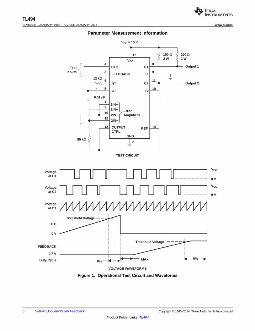
Dead-Time Control SectionSee Figure 1
PARAMETER TEST CONDITIONS MIN TYP (1) MAX UNITInput bias current (DEAD-TIME CTRL) VI = 0 to 5.25 V –2 –10 μA
VI (DEAD-TIME CTRL) = 0, CT = 0.01 μF,Maximum duty cycle, each output 45 %RT = 12 kΩZero duty cycle 3 3.3
Input threshold voltage (DEAD-TIME CTRL) VMaximum duty cycle 0
(1) All typical values, except for temperature coefficient, are at TA = 25°C.
PWM Comparator SectionSee Figure 1
PARAMETER TEST CONDITIONS MIN TYP (1) MAX UNITInput threshold voltage (FEEDBACK) Zero duty cyle 4 4.5 VInput sink current (FEEDBACK) V (FEEDBACK) = 0.7 V 0.3 0.7 mA
(1) All typical values, except for temperature coefficient, are at TA = 25°C.
Total DevicePARAMETER TEST CONDITIONS MIN TYP (1) MAX UNIT
VCC = 15 V 6 10RT = Vref,Standby supply current mAAll other inputs and outputs open VCC = 40 V 9 15Average supply current VI (DEAD-TIME CTRL) = 2 V, See Figure 1 7.5 mA
(1) All typical values, except for temperature coefficient, are at TA = 25°C.
Switching CharacteristicsTA = 25°C
PARAMETER TEST CONDITIONS MIN TYP (1) MAX UNITRise time 100 200 ns
Common-emitter configuration, See Figure 3Fall time 25 100 nsRise time 100 200 ns
Emitter-follower configuration, See Figure 4Fall time 40 100 ns
(1) All typical values, except for temperature coefficient, are at TA = 25°C.
Copyright © 1983–2014, Texas Instruments Incorporated Submit Documentation Feedback 5
Product Folder Links :TL494
TestInputs
DTC
FEEDBACK
RT
CT
GND50 kΩ
12 kΩ
0.01 µF
VCC
REFOUTPUTCTRL
E2
C2
E1
C1 Output 1
Output 2
150 Ω2 W
150 Ω2 W
VCC = 15 V
TEST CIRCUIT
1IN+
VCC
VCC
0 V
0 V
Voltageat C1
Voltageat C2
Voltageat CT
DTC
FEEDBACK
0 V
0.7 V
0% MAX 0%
Threshold V oltage
Threshold V oltage
VOLTAGE WAVEFORMS
Duty Cycle
ErrorAmplifiers
7
14
12
8
9
11
10
4
3
6
5
1
2
16
15
13
1IN−
2IN−
2IN+
TL494SLVS074F –JANUARY 1983–REVISED JANUARY 2014 www.ti.com
Parameter Measurement Information
Figure 1. Operational Test Circuit and Waveforms
6 Submit Documentation Feedback Copyright © 1983–2014, Texas Instruments Incorporated
Product Folder Links :TL494
Output
Each OutputCircuit
68 Ω2 W
15 V
CL = 15 pF(See Note A)
90%
10%
90%
10%
tftr
TEST CIRCUIT OUTPUT VOLTAGE WAVEFORM
NOTE A: CL includes probe and jig capacitance.
Output
Each OutputCircuit
68 Ω2 W
15 V
CL = 15 pF(See Note A)
90%
10%
90%
10%
tf tr
TEST CIRCUIT OUTPUT VOLTAGE WAVEFORM
NOTE A: CL includes probe and jig capacitance.
+
−
+
−
VI
Vref
FEEDBACK
Amplifier Under T est
Other Amplifier
TL494www.ti.com SLVS074F –JANUARY 1983–REVISED JANUARY 2014
Parameter Measurement Information
Figure 2. Amplifier Characteristics
Figure 3. Common-Emitter Configuration
Figure 4. Emitter-Follower Configuration
Copyright © 1983–2014, Texas Instruments Incorporated Submit Documentation Feedback 7
Product Folder Links :TL494
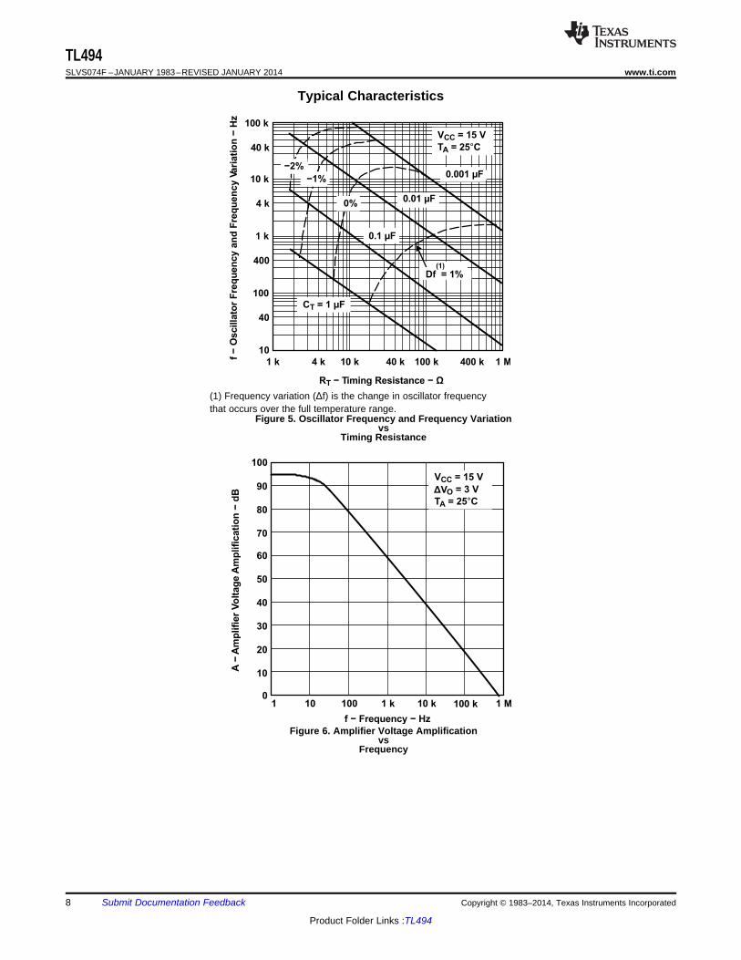
10
0
100
20
1 10 100 1 M
A−
Am
plifi
er
Vo
ltag
eA
mp
lifi
cati
on
−d
B
30
f − Frequency − Hz
1 k
VCC = 15 V
ΔVO = 3 V
TA = 25 C°
10 k
40
50
60
70
80
90
100 k
Df = 1%(1)
40
10
100
1 k 4 k 10 k 40 k 100 k 400 k 1 M
f−
Oscilla
tor
Fre
qu
en
cy a
nd
Fre
qu
en
cy V
ari
ati
on
−H
z
400
1 k
4 k
10 k
40 k
100 k
RT − Timing Resistance − Ω
0.1 Fµ
−2%
−1%
0%0.01 Fµ
0.001 Fµ
VCC = 15 V
TA = 25 C°
CT = 1 Fµ
TL494SLVS074F –JANUARY 1983–REVISED JANUARY 2014 www.ti.com
Typical Characteristics
(1) Frequency variation (Δf) is the change in oscillator frequencythat occurs over the full temperature range.
Figure 5. Oscillator Frequency and Frequency Variationvs
Timing Resistance
Figure 6. Amplifier Voltage Amplificationvs
Frequency
8 Submit Documentation Feedback Copyright © 1983–2014, Texas Instruments Incorporated
Product Folder Links :TL494
TL494www.ti.com SLVS074F –JANUARY 1983–REVISED JANUARY 2014
REVISION HISTORY
Changes from Revision E (February 2005) to Revision F Page
• Updated document to new TI data sheet format - no specification changes. ...................................................................... 1• Removed Ordering Information table. ................................................................................................................................... 1• Added ESD warning. ............................................................................................................................................................ 2
Copyright © 1983–2014, Texas Instruments Incorporated Submit Documentation Feedback 9
Product Folder Links :TL494
PACKAGE OPTION ADDENDUM
www.ti.com 10-Jun-2014
Addendum-Page 1
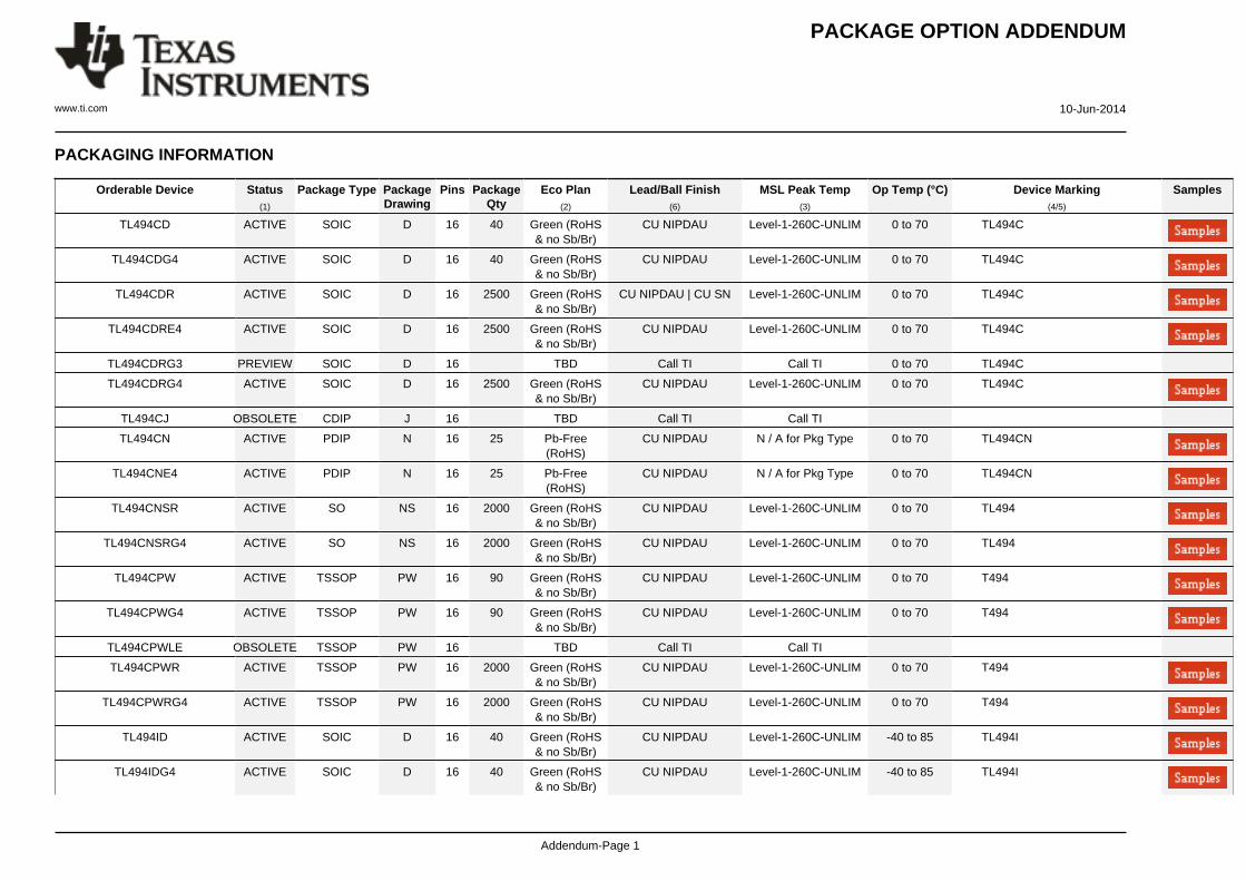
PACKAGING INFORMATION
Orderable Device Status(1)
Package Type PackageDrawing
Pins PackageQty
Eco Plan(2)
Lead/Ball Finish(6)
MSL Peak Temp(3)
Op Temp (°C) Device Marking(4/5)
Samples
TL494CD ACTIVE SOIC D 16 40 Green (RoHS& no Sb/Br)
CU NIPDAU Level-1-260C-UNLIM 0 to 70 TL494C
TL494CDG4 ACTIVE SOIC D 16 40 Green (RoHS& no Sb/Br)
CU NIPDAU Level-1-260C-UNLIM 0 to 70 TL494C
TL494CDR ACTIVE SOIC D 16 2500 Green (RoHS& no Sb/Br)
CU NIPDAU | CU SN Level-1-260C-UNLIM 0 to 70 TL494C
TL494CDRE4 ACTIVE SOIC D 16 2500 Green (RoHS& no Sb/Br)
CU NIPDAU Level-1-260C-UNLIM 0 to 70 TL494C
TL494CDRG3 PREVIEW SOIC D 16 TBD Call TI Call TI 0 to 70 TL494C
TL494CDRG4 ACTIVE SOIC D 16 2500 Green (RoHS& no Sb/Br)
CU NIPDAU Level-1-260C-UNLIM 0 to 70 TL494C
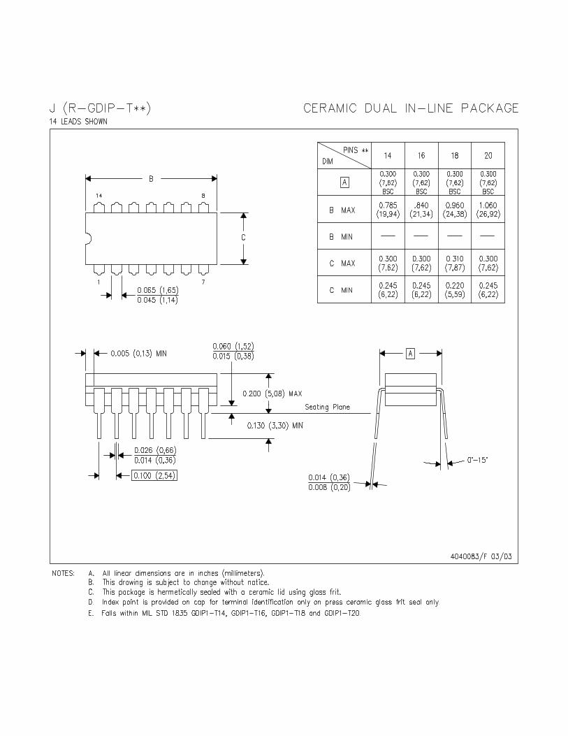
TL494CJ OBSOLETE CDIP J 16 TBD Call TI Call TI
TL494CN ACTIVE PDIP N 16 25 Pb-Free(RoHS)
CU NIPDAU N / A for Pkg Type 0 to 70 TL494CN
TL494CNE4 ACTIVE PDIP N 16 25 Pb-Free(RoHS)
CU NIPDAU N / A for Pkg Type 0 to 70 TL494CN
TL494CNSR ACTIVE SO NS 16 2000 Green (RoHS& no Sb/Br)
CU NIPDAU Level-1-260C-UNLIM 0 to 70 TL494
TL494CNSRG4 ACTIVE SO NS 16 2000 Green (RoHS& no Sb/Br)
CU NIPDAU Level-1-260C-UNLIM 0 to 70 TL494
TL494CPW ACTIVE TSSOP PW 16 90 Green (RoHS& no Sb/Br)
CU NIPDAU Level-1-260C-UNLIM 0 to 70 T494
TL494CPWG4 ACTIVE TSSOP PW 16 90 Green (RoHS& no Sb/Br)
CU NIPDAU Level-1-260C-UNLIM 0 to 70 T494
TL494CPWLE OBSOLETE TSSOP PW 16 TBD Call TI Call TI
TL494CPWR ACTIVE TSSOP PW 16 2000 Green (RoHS& no Sb/Br)
CU NIPDAU Level-1-260C-UNLIM 0 to 70 T494
TL494CPWRG4 ACTIVE TSSOP PW 16 2000 Green (RoHS& no Sb/Br)
CU NIPDAU Level-1-260C-UNLIM 0 to 70 T494
TL494ID ACTIVE SOIC D 16 40 Green (RoHS& no Sb/Br)
CU NIPDAU Level-1-260C-UNLIM -40 to 85 TL494I
TL494IDG4 ACTIVE SOIC D 16 40 Green (RoHS& no Sb/Br)
CU NIPDAU Level-1-260C-UNLIM -40 to 85 TL494I
PACKAGE OPTION ADDENDUM
www.ti.com 10-Jun-2014
Addendum-Page 2
Orderable Device Status(1)
Package Type PackageDrawing
Pins PackageQty
Eco Plan(2)
Lead/Ball Finish(6)
MSL Peak Temp(3)
Op Temp (°C) Device Marking(4/5)
Samples
TL494IDR ACTIVE SOIC D 16 2500 Green (RoHS& no Sb/Br)
CU NIPDAU | CU SN Level-1-260C-UNLIM -40 to 85 TL494I
TL494IDRE4 ACTIVE SOIC D 16 2500 Green (RoHS& no Sb/Br)
CU NIPDAU Level-1-260C-UNLIM -40 to 85 TL494I
TL494IDRG4 ACTIVE SOIC D 16 2500 Green (RoHS& no Sb/Br)
CU NIPDAU Level-1-260C-UNLIM -40 to 85 TL494I
TL494IN ACTIVE PDIP N 16 25 Pb-Free(RoHS)
CU NIPDAU N / A for Pkg Type -40 to 85 TL494IN
TL494INE4 ACTIVE PDIP N 16 25 Pb-Free(RoHS)
CU NIPDAU N / A for Pkg Type -40 to 85 TL494IN
TL494MJ OBSOLETE CDIP J 16 TBD Call TI Call TI -55 to 125
TL494MJB OBSOLETE CDIP J 16 TBD Call TI Call TI -55 to 125 (1) The marketing status values are defined as follows:ACTIVE: Product device recommended for new designs.LIFEBUY: TI has announced that the device will be discontinued, and a lifetime-buy period is in effect.NRND: Not recommended for new designs. Device is in production to support existing customers, but TI does not recommend using this part in a new design.PREVIEW: Device has been announced but is not in production. Samples may or may not be available.OBSOLETE: TI has discontinued the production of the device.
(2) Eco Plan - The planned eco-friendly classification: Pb-Free (RoHS), Pb-Free (RoHS Exempt), or Green (RoHS & no Sb/Br) - please check http://www.ti.com/productcontent for the latest availabilityinformation and additional product content details.TBD: The Pb-Free/Green conversion plan has not been defined.Pb-Free (RoHS): TI's terms "Lead-Free" or "Pb-Free" mean semiconductor products that are compatible with the current RoHS requirements for all 6 substances, including the requirement thatlead not exceed 0.1% by weight in homogeneous materials. Where designed to be soldered at high temperatures, TI Pb-Free products are suitable for use in specified lead-free processes.Pb-Free (RoHS Exempt): This component has a RoHS exemption for either 1) lead-based flip-chip solder bumps used between the die and package, or 2) lead-based die adhesive used betweenthe die and leadframe. The component is otherwise considered Pb-Free (RoHS compatible) as defined above.Green (RoHS & no Sb/Br): TI defines "Green" to mean Pb-Free (RoHS compatible), and free of Bromine (Br) and Antimony (Sb) based flame retardants (Br or Sb do not exceed 0.1% by weightin homogeneous material)
(3) MSL, Peak Temp. - The Moisture Sensitivity Level rating according to the JEDEC industry standard classifications, and peak solder temperature.
(4) There may be additional marking, which relates to the logo, the lot trace code information, or the environmental category on the device.
(5) Multiple Device Markings will be inside parentheses. Only one Device Marking contained in parentheses and separated by a "~" will appear on a device. If a line is indented then it is a continuationof the previous line and the two combined represent the entire Device Marking for that device.
PACKAGE OPTION ADDENDUM
www.ti.com 10-Jun-2014
Addendum-Page 3
(6) Lead/Ball Finish - Orderable Devices may have multiple material finish options. Finish options are separated by a vertical ruled line. Lead/Ball Finish values may wrap to two lines if the finishvalue exceeds the maximum column width.
Important Information and Disclaimer:The information provided on this page represents TI's knowledge and belief as of the date that it is provided. TI bases its knowledge and belief on informationprovided by third parties, and makes no representation or warranty as to the accuracy of such information. Efforts are underway to better integrate information from third parties. TI has taken andcontinues to take reasonable steps to provide representative and accurate information but may not have conducted destructive testing or chemical analysis on incoming materials and chemicals.TI and TI suppliers consider certain information to be proprietary, and thus CAS numbers and other limited information may not be available for release.
In no event shall TI's liability arising out of such information exceed the total purchase price of the TI part(s) at issue in this document sold by TI to Customer on an annual basis.
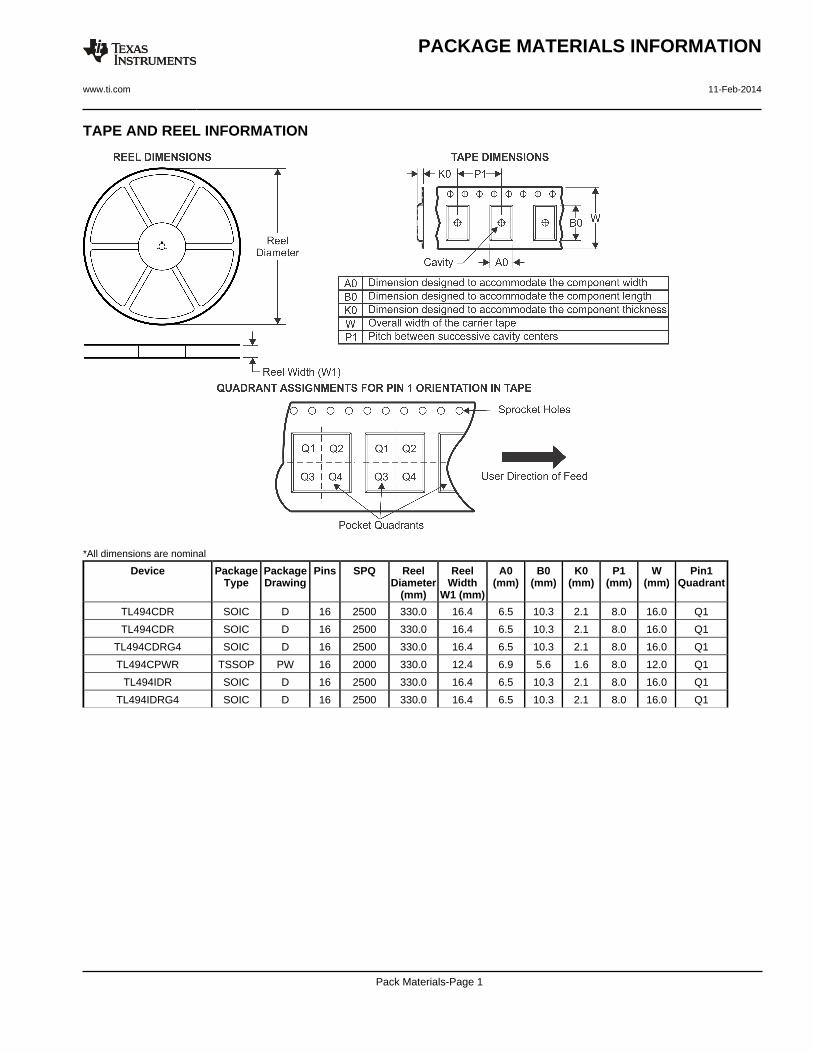
TAPE AND REEL INFORMATION
*All dimensions are nominal
Device PackageType
PackageDrawing
Pins SPQ ReelDiameter
(mm)
ReelWidth
W1 (mm)
A0(mm)
B0(mm)
K0(mm)
P1(mm)
W(mm)
Pin1Quadrant
TL494CDR SOIC D 16 2500 330.0 16.4 6.5 10.3 2.1 8.0 16.0 Q1
TL494CDR SOIC D 16 2500 330.0 16.4 6.5 10.3 2.1 8.0 16.0 Q1
TL494CDRG4 SOIC D 16 2500 330.0 16.4 6.5 10.3 2.1 8.0 16.0 Q1
TL494CPWR TSSOP PW 16 2000 330.0 12.4 6.9 5.6 1.6 8.0 12.0 Q1
TL494IDR SOIC D 16 2500 330.0 16.4 6.5 10.3 2.1 8.0 16.0 Q1
TL494IDRG4 SOIC D 16 2500 330.0 16.4 6.5 10.3 2.1 8.0 16.0 Q1
PACKAGE MATERIALS INFORMATION
www.ti.com 11-Feb-2014
Pack Materials-Page 1
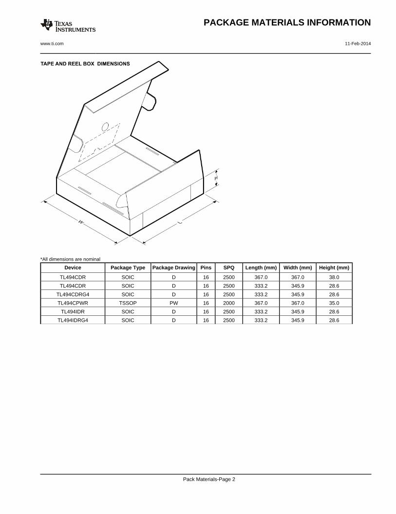
*All dimensions are nominal
Device Package Type Package Drawing Pins SPQ Length (mm) Width (mm) Height (mm)
TL494CDR SOIC D 16 2500 367.0 367.0 38.0
TL494CDR SOIC D 16 2500 333.2 345.9 28.6
TL494CDRG4 SOIC D 16 2500 333.2 345.9 28.6
TL494CPWR TSSOP PW 16 2000 367.0 367.0 35.0
TL494IDR SOIC D 16 2500 333.2 345.9 28.6
TL494IDRG4 SOIC D 16 2500 333.2 345.9 28.6
PACKAGE MATERIALS INFORMATION
www.ti.com 11-Feb-2014
Pack Materials-Page 2
IMPORTANT NOTICETexas Instruments Incorporated and its subsidiaries (TI) reserve the right to make corrections, enhancements, improvements and otherchanges to its semiconductor products and services per JESD46, latest issue, and to discontinue any product or service per JESD48, latestissue. Buyers should obtain the latest relevant information before placing orders and should verify that such information is current andcomplete. All semiconductor products (also referred to herein as “components”) are sold subject to TI’s terms and conditions of salesupplied at the time of order acknowledgment.TI warrants performance of its components to the specifications applicable at the time of sale, in accordance with the warranty in TI’s termsand conditions of sale of semiconductor products. Testing and other quality control techniques are used to the extent TI deems necessaryto support this warranty. Except where mandated by applicable law, testing of all parameters of each component is not necessarilyperformed.TI assumes no liability for applications assistance or the design of Buyers’ products. Buyers are responsible for their products andapplications using TI components. To minimize the risks associated with Buyers’ products and applications, Buyers should provideadequate design and operating safeguards.TI does not warrant or represent that any license, either express or implied, is granted under any patent right, copyright, mask work right, orother intellectual property right relating to any combination, machine, or process in which TI components or services are used. Informationpublished by TI regarding third-party products or services does not constitute a license to use such products or services or a warranty orendorsement thereof. Use of such information may require a license from a third party under the patents or other intellectual property of thethird party, or a license from TI under the patents or other intellectual property of TI.Reproduction of significant portions of TI information in TI data books or data sheets is permissible only if reproduction is without alterationand is accompanied by all associated warranties, conditions, limitations, and notices. TI is not responsible or liable for such altereddocumentation. Information of third parties may be subject to additional restrictions.Resale of TI components or services with statements different from or beyond the parameters stated by TI for that component or servicevoids all express and any implied warranties for the associated TI component or service and is an unfair and deceptive business practice.TI is not responsible or liable for any such statements.Buyer acknowledges and agrees that it is solely responsible for compliance with all legal, regulatory and safety-related requirementsconcerning its products, and any use of TI components in its applications, notwithstanding any applications-related information or supportthat may be provided by TI. Buyer represents and agrees that it has all the necessary expertise to create and implement safeguards whichanticipate dangerous consequences of failures, monitor failures and their consequences, lessen the likelihood of failures that might causeharm and take appropriate remedial actions. Buyer will fully indemnify TI and its representatives against any damages arising out of the useof any TI components in safety-critical applications.In some cases, TI components may be promoted specifically to facilitate safety-related applications. With such components, TI’s goal is tohelp enable customers to design and create their own end-product solutions that meet applicable functional safety standards andrequirements. Nonetheless, such components are subject to these terms.No TI components are authorized for use in FDA Class III (or similar life-critical medical equipment) unless authorized officers of the partieshave executed a special agreement specifically governing such use.Only those TI components which TI has specifically designated as military grade or “enhanced plastic” are designed and intended for use inmilitary/aerospace applications or environments. Buyer acknowledges and agrees that any military or aerospace use of TI componentswhich have not been so designated is solely at the Buyer's risk, and that Buyer is solely responsible for compliance with all legal andregulatory requirements in connection with such use.TI has specifically designated certain components as meeting ISO/TS16949 requirements, mainly for automotive use. In any case of use ofnon-designated products, TI will not be responsible for any failure to meet ISO/TS16949.Products ApplicationsAudio www.ti.com/audio Automotive and Transportation www.ti.com/automotiveAmplifiers amplifier.ti.com Communications and Telecom www.ti.com/communicationsData Converters dataconverter.ti.com Computers and Peripherals www.ti.com/computersDLP® Products www.dlp.com Consumer Electronics www.ti.com/consumer-appsDSP dsp.ti.com Energy and Lighting www.ti.com/energyClocks and Timers www.ti.com/clocks Industrial www.ti.com/industrialInterface interface.ti.com Medical www.ti.com/medicalLogic logic.ti.com Security www.ti.com/securityPower Mgmt power.ti.com Space, Avionics and Defense www.ti.com/space-avionics-defenseMicrocontrollers microcontroller.ti.com Video and Imaging www.ti.com/videoRFID www.ti-rfid.comOMAP Applications Processors www.ti.com/omap TI E2E Community e2e.ti.comWireless Connectivity www.ti.com/wirelessconnectivity
Mailing Address: Texas Instruments, Post Office Box 655303, Dallas, Texas 75265Copyright © 2014, Texas Instruments Incorporated