
TITLE : HV101HD1 -1E1 Preliminary Product...
29
TD-0008247 (1/3) A4(210 X 297) SPEC. NUMBER PRODUCT GROUP REV. ISSUE DATE PAGE TITLE : HV101HD1 - 1E1 Preliminary Product Specification A4(210 X 297) PAGE HYDIS Technologies OF 30 2012. 05. 23 P0 TFT LCD P R O P R I E T A R Y N O T E THIS SPECIFICATION IS THE PROPERTY OF HYDIS AND SHALL NOT BE REPRODUCED OR COPIED WITHOUT THE WRITTEN PERMISSION OF HYDIS AND MUST BE RETURNED TO HYDIS UPON ITS REQUEST 1 FOR MORE INFORMATION: AZ DISPLAYS, INC. 75 COLUMBIA, ALISO VIEJO, CA 92656 PHONE: (949) 360 5830 E-MAIL: [email protected] Website: www.azdisplays.com
Transcript of TITLE : HV101HD1 -1E1 Preliminary Product...

TD-0008247 (1/3) A4(210 X 297)
SPEC. NUMBER
PRODUCT GROUP REV. ISSUE DATE PAGE
TITLE : HV101HD1 - 1E1
Preliminary Product Speci�cation
A4(210 X 297)
PAGE
HYDIS Technologies
OF 30 2012. 05. 23 P0 TFT LCD
PR OPR IE TAR Y NOTE THIS SPECIFICATION IS THE PROPERTY OF HYDIS AND SHALL NOT BE REPRODUCED OR COPIED WITHOUT THE WRITTEN PERMISSION OF HYDIS AND MUST BE RETURNED TO HYDIS UPON ITS REQUEST
1
FOR MORE INFORMATION: AZ DISPLAYS, INC. 75 COLUMBIA, ALISO VIEJO, CA 92656 PHONE: (949) 360 5830 E-MAIL: [email protected] Website: www.azdisplays.com

TD-0008247 (2/3) A4(210 X 297)
REVISION HISTORY
PRODUCT GROUP REV ISSUE DATE
TFT LCD PRODUCT P0 2012. 05. 23
SPEC. NUMBER
SPEC TITLE
HV101HD1-1E1 Preliminary Product Specification PAGE
REV. ECN NO. DESCRIPTION OF CHANGES DATE PREPARED
P0 Initial Release 12. 05. 23 SH Kim
OF 30 2

TD-0008247 (3/3) A4(210 X 297)
PRODUCT GROUP REV ISSUE DATE
TFT LCD PRODUCT P0 2012. 05. 23
SPEC. NUMBER SPEC TITLE
HV101HD1-1E1 Preliminary Product Specification PAGE
OF 30 3
Contents
No Item Page
1.0 General Description 4
2.0 Absolute Maximum Ratings 6
3.0 Electrical Specifications 7
4.0 Optical Specifications 11
5.0 Interface Connections 16
6.0 Signal Timing Specifications 19
7.0 Signal Timing Waveforms 19
8.0 Input Signals, Basic Display Colors & Gray Scale of Colors 20
9.0 Power Sequence 21
10.0 Mechanical Characteristics 22
11.0 Mechanical Drawing 23
12.0 Reliability Test 25
13.0 Handling & Cautions 26
14.0 Labels 27
15.0 Packing Information 29

TD-0008247 (3/3) A4(210 X 297)
PRODUCT GROUP REV ISSUE DATE
TFT LCD PRODUCT P0 2012. 05. 23
SPEC. NUMBER SPEC TITLE
HV101HD1-1E1 Preliminary Product Specification PAGE
OF 30 4
1.0 GENERAL DESCRIPTION
1.1 Introduction
HV101HD1-1E1 is a color active matrix TFT LCD module using amorphous silicon TFT's
(Thin Film Transistors) as an active switching devices. This module has a 10.1 inch
diagonally measured active area with HD resolutions (1366 horizontal by 768 vertical
pixel array). Each pixel is divided into RED, GREEN, BLUE dots which are arranged in
vertical Stripe and this module can display 16.7M colors. The TFT-LCD panel used for this
module is a low reflection and higher color type.
1.2 Features
FAB Site : CPT
3.3 V Logic Power
LVDS Interface (1channel)
16.7M Colors (8bit)
Data Enable Signal Mode
SMD LED (36EA) Bottom alignment
Green Product (RoHS) & Halogen free
Ga
te D
rive
r
Source Driver
TFT LCD Panel
1366×RGB X 768
LVDS Input Signal
VDD
Ba
ck L
igh
t
(SM
D L
ED
Arra
y)
VLED
DC/DC
TCON
LED
Driver LED_EN
Co
nn
ecto
r (CN
1)
Anode/Cathode
LED_PWM
PW
M

TD-0008247 (3/3) A4(210 X 297)
PRODUCT GROUP REV ISSUE DATE
TFT LCD PRODUCT P0 2012. 05. 23
SPEC. NUMBER SPEC TITLE
HV101HD1-1E1 Preliminary Product Specification PAGE
OF 30 5
1.4 General Specifications
Parameter Specification Unit Remark
Active area 223.341(H) ×125.568(V) mm
Number of pixels 1366(H) ×RGB X 768(V) pixels
Pixel pitch 0.1635 × 0.1635 mm
Pixel arrangement RGB Vertical Stripe
Display colors 16.7M (8bit) colors
Display mode Normally Black
Outline dimension 234.53.0.3(H)×138.970.3(V)×2.40.2(D) mm
Weight 115 (Max.) g
Back-light Bottom alignment, 36-LEDs type
1.3 Application
industrial tablet
< Table 1. General Specifications >

TD-0008247 (3/3) A4(210 X 297)
PRODUCT GROUP REV ISSUE DATE
TFT LCD PRODUCT P0 2012. 05. 23
SPEC. NUMBER SPEC TITLE
HV101HD1-1E1 Preliminary Product Specification PAGE
OF 30 6
2.0 ABSOLUTE MAXIMUM RATINGS
The followings are maximum values which, if exceed, may cause faulty operation or
damage to the unit.
Parameter Symbol Min. Max. Unit Remarks
Logic Power Supply Voltage VDD -0.3 4.0 V
Logic Power Supply Voltage VCC -0.3 2.0 V
Back-light Power Supply Voltage HVDD -0.3 40 V
Back-light LED Current ILED 30.0 mA Note 1
Back-light LED Reverse Voltage VR - TBD V
Operating Temperature TOP -0 +50 ℃ Note 1,
Note 2 Storage Temperature TSP -20 +60 ℃
Note 1. Ambient temperature vs allowable forward current are shown in the figure below.
Note 2. Temperature and relative humidity range are shown in the figure below.
90% RH Max. ( 40℃ ≥ Ta)
Maximum wet - bulb temperature at 39℃ or less. ( > 40℃) No condensation.
Ta=25+/-2°C < Table 2. Absolute Maximum Ratings >

TD-0008247 (3/3) A4(210 X 297)
PRODUCT GROUP REV ISSUE DATE
TFT LCD PRODUCT P0 2012. 05. 23
SPEC. NUMBER SPEC TITLE
HV101HD1-1E1 Preliminary Product Specification PAGE
OF 30 7
3.0 ELECTRICAL SPECIFICATIONS 3.1 Electrical Specifications
Parameter Min. Typ. Ma
x. Unit Remarks
Logic Power Supply Voltage VDD - 3.3 - V
Logic Power Supply Current IDD - TBD - mA Vdd=3.3V, 25℃ Note 1
Back-light LED Voltage / Back-light LED Total Voltage
VLED
/VBL 2.8/ 16.8
2.9/ 17.4
3.0/ 18.0
V
Back-light LED Current / Back-light LED Total Current
ILED
/IBL -
17/ 102
- mA
Power Consumption
PDD - TBD - W
Note 2
Pcc - TBD - W
PBL 2.02 2.10 2.16 W
< Table 3. Electrical Specifications >
Notes : 1. The supply voltage is measured and specified at the interface connector of LCM.
( Test Pattern : White)
2. Calculated value for reference (VLED × ILED × # of LEDs (36EA) ).
This value is with LED driver efficiency (85%)

TD-0008247 (3/3) A4(210 X 297)
PRODUCT GROUP REV ISSUE DATE
TFT LCD PRODUCT P0 2012. 05. 23
SPEC. NUMBER SPEC TITLE
HV101HD1-1E1 Preliminary Product Specification PAGE
OF 30 8
3.2 PWM Duty Ratio vs Brightness
0
10
20
30
40
50
60
70
80
90
100
0 10 20 30 40 50 60 70 80 90 100
Duty Ratio (%)
Re
lative
Bri
gh
tne
ss (
%)
Notes :
In case of duty ratio 0%, LED can’t illuminate itself so this state is LED off.
In case of duty ratio 100%, the brightness of LED is maximum and the state is LED on.

TD-0008247 (3/3) A4(210 X 297)
PRODUCT GROUP REV ISSUE DATE
TFT LCD PRODUCT P0 2012. 05. 23
SPEC. NUMBER SPEC TITLE
HV101HD1-1E1 Preliminary Product Specification PAGE
OF 30
3.3 LVDS Interface
9
< Table 9, LVDS Rx Interface Timing Specification>
tRIP5
tRIP4
tRIP3
tRIP2
tRIP6
tRIP1
tRIP0
Rx Rx Rx Rx Rx Rx Rx Rx Rx Rx Rx
tRCIP
Vdiff=0[v] Vdiff=0[v] RxCLKIN+/-
RxINz +/-
* Z = 0, 1, 2
Item Symbol Min. Typ. Max. Unit Remarks
CLKIN Period tRCIP - 12.43 - nsec
Input Data 0 tRIP0 -0.4 0.0 +0.4 nsec
Input Data 1 tRIP1 tRICP/7-0.4 tRICP/7 tRICP/7+0.4 nsec
Input Data 2 tRIP2 2 ×tRICP/7-0.4 2 ×tRICP/7 2 ×tRICP/7+0.4 nsec
Input Data 3 tRIP3 3 ×tRICP/7-0.4 3 ×tRICP/7 3 ×tRICP/7+0.4 nsec
Input Data 4 tRIP4 4 ×tRICP/7-0.4 4 ×tRICP/7 4 ×tRICP/7+0.4 nsec
Input Data 5 tRIP5 5 ×tRICP/7-0.4 5 ×tRICP/7 5 ×tRICP/7+0.4 nsec
Input Data 6 tRIP6 6 ×tRICP/7-0.4 6 ×tRICP/7 6 ×tRICP/7+0.4 nsec
The specification of the LVDS Rx interface timing parameter

TD-0008247 (3/3) A4(210 X 297)
PRODUCT GROUP REV ISSUE DATE
TFT LCD PRODUCT P0 2012. 05. 23
SPEC. NUMBER SPEC TITLE
HV101HD1-1E1 Preliminary Product Specification PAGE
OF 30 10
4.0 OPTICAL SPECIFICATIONS
4.1 Overview
The test of optical specifications shall be measured in a dark room (ambient luminance 1
lux and temperature = 252℃) with the equipment of Luminance meter system (Goniometer
system and TOPCON BM-5A) and test unit shall be located at an approximate distance
50cm from the LCD surface at a viewing angle of θ and Φ equal to 0. We refer to θØ =0
(=θ3 ) as the 3 o’clock direction (the “right”), θØ =90 (= θ12 ) as the 12 o’clock direction
(“upward”), θØ =180 (= θ9 ) as the 9 o’clock direction (“left”) and θØ =270(= θ6 ) as the 6
o’clock direction (“bottom”). While scanning θ and/or Ø, the center of the measuring spot on
the Display surface shall stay fixed. The backlight should be operating for 30 minutes prior to
measurement. VDD shall be 3.3+/- 0.3V at 25C.
Parameter Symbol Condition Min. Typ. Max. Unit Remarks
Viewing Angle
range
Horizontal Θ3
CR > 10
80 89 - Deg.
Note 1 Θ9 80 89 - Deg.
Vertical Θ12 80 89 - Deg.
Θ6 80 89 - Deg.
Luminance Contrast ratio CR Θ = 0 500 800 - Note 2
Luminance of
White 1 Points Yw Θ = 0 350 400 - cd/m2 Note 4
White Luminance
uniformity 9 Points ΔY9 75 - - % Note 4
White Chromaticity Wx Θ = 0
TBD -
Note 3
Wy TBD -
Reproduction
of color
Red Rx
Θ = 0
- -
Ry - -
Green Gx - -
Gy - -
Blue Bx - -
By - -
NTSC 50 %
Response
Time
Total
(Tr + Td)
Ta= 25 C
Θ = 0 - - 30 ms Note 5
Cross Talk CT Θ = 0 - - 2.0 % Note 6
4.2 Optical Specifications <Table 6. Optical Specifications>

TD-0008247 (3/3) A4(210 X 297)
PRODUCT GROUP REV ISSUE DATE
TFT LCD PRODUCT P0 2012. 05. 23
SPEC. NUMBER SPEC TITLE
HV101HD1-1E1 Preliminary Product Specification PAGE
OF 30 11
Notes :
1. Viewing angle is the angle at which the contrast ratio is greater than 10. The viewing
angles are determined for the horizontal or 3, 9 o’clock direction and the vertical or 6,
12 o’clock direction with respect to the optical axis which is normal to the LCD surface
(see Figure1).
2. Contrast measurements shall be made at viewing angle of Θ= 0 and at the center of
the LCD surface. Luminance shall be measured with all pixels in the view field set first
to white, then to the dark (black) state (see Figure1). Luminance Contrast Ratio (CR) is
defined mathematically as CR = Luminance when displaying a white raster / Luminance
when displaying a black raster.
3. Reference only / Standard Front Surface Treatment Measured with green cover glass.
The color chromaticity coordinates specified in Table 4 shall be calculated from the
spectral data measured with all pixels first in red, green, blue and white. Measurements
shall be made at the center of the panel.

TD-0008247 (3/3) A4(210 X 297)
PRODUCT GROUP REV ISSUE DATE
TFT LCD PRODUCT P0 2012. 05. 23
SPEC. NUMBER SPEC TITLE
HV101HD1-1E1 Preliminary Product Specification PAGE
OF 30 12
Figure 1. Measurement Set Up
Figure 2. White Luminance and Uniformity Measurement Locations (9 points)
Optical characteristics measurement setup
Center of the screen
TFT-LCD module LCD panel
Photo detector
( TOPCON BM-5A)
50 cm Field = 1
o
4.3 Optical Measurements
Note 4. Luminance of white is defined as luminance values of 9 points across the LCD
surface. Luminance shall be measured with all pixels in the view field set first to
white. This measurement shall be taken at the locations shown in Figure 2 for a
total of the measurements per display.
* Yw = (Sum of 9 Points Luminance / 9 )
* LED Condition = (Duty Ratio 100%, LED current 17 mA)
Column
Row 10mm 683 10mm
10mm
384
10mm

TD-0008247 (3/3) A4(210 X 297)
PRODUCT GROUP REV ISSUE DATE
TFT LCD PRODUCT P0 2012. 05. 23
SPEC. NUMBER SPEC TITLE
HV101HD1-1E1 Preliminary Product Specification PAGE
OF 30 13
Figure 3. Response Time Testing
TFT Off(Black) TFT On(White) TFT Off(Black)
Tr
100%
90%
10%
0%
Td

TD-0008247 (3/3) A4(210 X 297)
PRODUCT GROUP REV ISSUE DATE
TFT LCD PRODUCT P0 2012. 05. 23
SPEC. NUMBER SPEC TITLE
HV101HD1-1E1 Preliminary Product Specification PAGE
OF 30 14
YA (1680,600) L256
YB(1680, 600)
960,300 L31
480,300
YB - YA
YB Cross-Talk (%) = × 100
Figure 4. Cross Modulation Test Description
VIEW AREA
Where:
YA = Initial luminance of measured area (cd/m2)
YB = Subsequent luminance of measured area (cd/m2)
The location measured will be exactly the same in both patterns
VIEW AREA
Note 5. The electro-optical response time measurements shall be made as Figure 4 by
switching the “data” input signal ON and OFF. The times needed for the luminance
to change from 10% to 90% is Tr, and 90% to 10% is Td.
Note 6. Cross-Talk of one area of the LCD surface by another shall be measured by
comparing the luminance (YA) of a 25mm diameter area, with all display pixels set
to a gray level, to the luminance (YB) of that same area when any adjacent area is
driven dark (Refer to Figure 4).
960,600 480,600

TD-0008247 (3/3) A4(210 X 297)
PRODUCT GROUP REV ISSUE DATE
TFT LCD PRODUCT P0 2012. 05. 23
SPEC. NUMBER SPEC TITLE
HV101HD1-1E1 Preliminary Product Specification PAGE
OF 30
5.0 INTERFACE CONNECTIONS
5.1 Electrical Interface Connection
< Table 7, Electrical Interface Connection >
CN1 HYDIS side connector I-PEX : 20455-040E-12
Pin No Symbol Function
1 NC NC (Please let it floating for test only)
2 VCC +3.3V Power
3 VCC +3.3V Power
4 V_EDID EDID 3.3V Power
5 NC NC (Please let it floating for test only)
6 CLK_EDID EDID Clock
7 DATA_EDID EDID Data
8 RXIN0- LVDS Signal(-)—channel 0
9 RXIN0+ LVDS Signal(+)—channel 0
10 GND Ground
11 RXIN1- LVDS Signal(-)—channel 1
12 RXIN1+ LVDS Signal(+)—channel 1
13 GND Ground
14 RXIN2- LVDS Signal(-)—channel 2
15 RXIN2+ LVDS Signal(+)—channel 2
16 GND Ground
17 RXCLKIN- LVDS Clock Signal(-)
18 RXCLKIN+ LVDS Clock Signal(+)
19 GND Ground
20 RXIN3- LVDS Signal(-)—channel 3
21 RXIN3+ LVDS Signal(+)—channel 3

TD-0008247 (3/3) A4(210 X 297)
PRODUCT GROUP REV ISSUE DATE
TFT LCD PRODUCT P0 2012. 05. 23
SPEC. NUMBER SPEC TITLE
HV101HD1-1E1 Preliminary Product Specification PAGE
OF 30 16
< Table 7, Electrical Interface Connection >
Pin No Symbol Function
22 GND Ground
23 NC NC (Please let it floating for test only)
24 NC NC (Please let it floating for test only)
25 GND Ground
26 NC NC (Please let it floating for test only)
27 NC NC (Please let it floating for test only)
28 GND Ground
29 NC NC (Please let it floating for test only)
30 NC NC (Please let it floating for test only)
31 VSSLED Ground – LED
32 VSSLED Ground – LED
33 VSSLED Ground – LED
34 NC NC (Please let it floating for test only)
35 PWM System PWM Signal Input (+3.3V Swing)
36 LED_EN LED enable pin (+3.3V Input)
37 NC NC (Please let it floating for test only)
38 VLED Power Supply for LED(VLED =4.5V ~ 21V)
39 VLED Power Supply for LED(VLED =4.5V ~ 21V)
40 VLED Power Supply for LED(VLED =4.5V ~ 21V)

TD-0008247 (3/3) A4(210 X 297)
PRODUCT GROUP REV ISSUE DATE
TFT LCD PRODUCT P0 2012. 05. 23
SPEC. NUMBER SPEC TITLE
HV101HD1-1E1 Preliminary Product Specification PAGE
OF 30 17
5.2 Data Input Format
R G B R G B R G B R G B
1 Pixel = 3 Dots
R G B
R G B R G B R G B R G B
(1, 1) (2, 1) (1365, 1) (1366, 1)
(1, 768) (2, 768) (1365, 768) (1366, 768)

TD-0008247 (3/3) A4(210 X 297)
PRODUCT GROUP REV ISSUE DATE
TFT LCD PRODUCT P0 2012. 05. 23
SPEC. NUMBER SPEC TITLE
HV101HD1-1E1 Preliminary Product Specification PAGE
OF 30 18
6.0. SIGNAL TIMING SPECIFICATIONS
6.1 The LCM is operated by the only DE (Data enable) mode
7.0 SIGNAL TIMING WAVEFORMS
7.1 Timing Waveforms of Interface Signal
Valid display data (768 Clocks)
T1
T2
T3
T4
T5
DE
DCLK
DE
DATA SIGNALS
< Table 8. Signal Timing >
Note 1. This value only guarantee for the circuit-operation
Item Symbol Min. Typ. Max. Unit
Frame Rate - 60 Hz
Frame Period T1 838 Lines
Vertical Display Time T2 768 Lines
Vertical Blanking Time T3 70 Lines
1 Line Scanning Time T4 1600 Clocks
Horizontal Display Time T5 1366 Clocks
Horizontal Blanking Time T6 243 Clocks
Clock Rate 1/T7 80.44 MHz

TD-0008247 (3/3) A4(210 X 297)
PRODUCT GROUP REV ISSUE DATE
TFT LCD PRODUCT P0 2012. 05. 23
SPEC. NUMBER SPEC TITLE
HV101HD1-1E1 Preliminary Product Specification PAGE
OF 30 19
8.0 INPUT SIGNALS, BASIC DISPLAY COLORS & GRAY SCALE OF
COLORS Each color is displayed in sixty-four gray scales from a 8 bit data signal input.
Colors & Gray Scale
Red Data Green Data Blue Data
R5 R4 R3 R2 R1 R0 G5 G4 G3 G2 G1 G0 B5 B4 B3 B2 B1 B0
Basic Colors
Black 0 0 0 0 0 0 0 0 0 0 0 0 0 0 0 0 0 0
Blue 0 0 0 0 0 0 0 0 0 0 0 0 1 1 1 1 1 1
Green 0 0 0 0 0 0 1 1 1 1 1 1 0 0 0 0 0 0
Cyan 0 0 0 0 0 0 1 1 1 1 1 1 1 1 1 1 1 1
Red 1 1 1 1 1 1 0 0 0 0 0 0 0 0 0 0 0 0
Magenta 1 1 1 1 1 1 0 0 0 0 0 0 1 1 1 1 1 1
Yellow 1 1 1 1 1 1 1 1 1 1 1 1 0 0 0 0 0 0
White 1 1 1 1 1 1 1 1 1 1 1 1 1 1 1 1 1 1
Gray Scale
Of Red
Black 0 0 0 0 0 0 0 0 0 0 0 0 0 0 0 0 0 0
△ 0 0 0 0 0 1 0 0 0 0 0 0 0 0 0 0 0 0
Darker 0 0 0 0 1 0 0 0 0 0 0 0 0 0 0 0 0 0
△ ↓ ↓ ↓
▽ ↓ ↓ ↓
Brighter 1 1 1 1 0 1 0 0 0 0 0 0 0 0 0 0 0 0
▽ 1 1 1 1 1 0 0 0 0 0 0 0 0 0 0 0 0 0
Red 1 1 1 1 1 1 0 0 0 0 0 0 0 0 0 0 0 0
Gray Scale
Of Green
Black 0 0 0 0 0 0 0 0 0 0 0 0 0 0 0 0 0 0
△ 0 0 0 0 0 0 0 0 0 0 0 1 0 0 0 0 0 0
Darker 0 0 0 0 0 0 0 0 0 0 1 0 0 0 0 0 0 0
△ ↓ ↓ ↓
▽ ↓ ↓ ↓
Brighter 0 0 0 0 0 0 1 1 1 1 0 1 0 0 0 0 0 0
▽ 0 0 0 0 0 0 1 1 1 1 1 0 0 0 0 0 0 0
Green 0 0 0 0 0 0 1 1 1 1 1 1 0 0 0 0 0 0
Gray Scale
Of Blue
Black 0 0 0 0 0 0 0 0 0 0 0 0 0 0 0 0 0 0
△ 0 0 0 0 0 0 0 0 0 0 0 0 0 0 0 0 0 1
Darker 0 0 0 0 0 0 0 0 0 0 0 0 0 0 0 0 1 0
△ ↓ ↓ ↓
▽ ↓ ↓ ↓
Brighter 0 0 0 0 0 0 0 0 0 0 0 0 1 1 1 1 0 1
▽ 0 0 0 0 0 0 0 0 0 0 0 0 1 1 1 1 1 0
Blue 0 0 0 0 0 0 0 0 0 0 0 0 1 1 1 1 1 1
Gray Scale
Of White
& Black
Black 0 0 0 0 0 0 0 0 0 0 0 0 0 0 0 0 0 0
△ 0 0 0 0 0 1 0 0 0 0 0 1 0 0 0 0 0 1
Darker 0 0 0 0 1 0 0 0 0 0 1 0 0 0 0 0 1 0
△ ↓ ↓ ↓
▽ ↓ ↓ ↓
Brighter 1 1 1 1 0 1 1 1 1 1 0 1 1 1 1 1 0 1
▽ 1 1 1 1 1 0 1 1 1 1 1 0 1 1 1 1 1 0
White 1 1 1 1 1 1 1 1 1 1 1 1 1 1 1 1 1 1

TD-0008247 (3/3) A4(210 X 297)
PRODUCT GROUP REV ISSUE DATE
TFT LCD PRODUCT P0 2012. 05. 23
SPEC. NUMBER SPEC TITLE
HV101HD1-1E1 Preliminary Product Specification PAGE
OF 30
T1
Valid
T2
T5
T3 T4
0.9VDD/0.9VCC
0.1VDD/ 0.1VCC 0V
0V
0V
T7
T6
0.9VDD/0.9VCC
0.1VDD/ 0.1VCC
20
9.0 POWER SEQUENCE To prevent a latch-up or DC operation of the LCD module, the power on/off sequence shall
be as shown in below
Power Supply
Interface Signal
Back- light
● T1 10 ms
● 0 T2 50 ms
● 70 ms T3
● 200 ms T4
● 0 T5 ≤ 50 ms
● 0 T6 10ms
● 150ms T7
Notes : 1. When the power supply VDD/ VCC is 0V, Keep the level of input signals
on the low or keep
high impedance.
2. Do not keep the interface signal high impedance when power is on.
3. Back Light must be turn on after power for logic and interface signal are valid.

TD-0008247 (3/3) A4(210 X 297)
PRODUCT GROUP REV ISSUE DATE
TFT LCD PRODUCT P0 2012. 05. 23
SPEC. NUMBER SPEC TITLE
HV101HD1-1E1 Preliminary Product Specification PAGE
OF 30 21
10.0 MECHANICAL CHARACTERISTICS 10.1 Dimensional Requirements
Figure 5 & 6 shows mechanical outlines for the model
Parameter Specification Unit
Active Area 223.341(H) ×125.568(V) mm
Number of pixels 1366(H) X 768(V) (1 pixel = R + G + B dots)
Pixel pitch 0.1635(H) X 0.1635(V) mm
Pixel arrangement RGB Vertical stripe
Display colors 262K (6bits)
Display mode Normally Black
Outline dimension 234.53(H)×138.97(V)×2.4(D) (Typ.) mm
Weight 115(Max.) g
Back-light Bottom alignment 36-LEDs type
10.2 LR and Polarizer Hardness.
The surface of the LCD has an Clear and a coating to reduce scratching.
10.3 Light Leakage
There shall not be visible light from the back-lighting system around the edges of the
screen as seen from a distance 50cm from the screen with an overhead light level of
150lux. The manufacture shall furnish limit samples of the panel showing the light leakage
acceptable.
< Table 9, Mechanical Characters >

TD-0008247 (3/3) A4(210 X 297)
PRODUCT GROUP REV ISSUE DATE
TFT LCD PRODUCT P0 2012. 05. 23
SPEC. NUMBER SPEC TITLE
HV101HD1-1E1 Preliminary Product Specification PAGE
OF 30 22
Figure 5. TFT-LCD Module Outline Dimension (Front View)
11.0 Mechanical Drawing
TO
P
BO
TT
OM
125.568 (active area)
234.5
3±0.2 (O
utlin
e)
(67.01)
35.61862.784
2-11.91(D-IC)
4.5
2 (to
Po
l.)2.16 (to Pol.)
(118.2
6)
227.4
9±0.2 (P
ol.)
129.71±0.2 (Pol.)
Shie
ld c
over
Activ
e A
rea C
ente
r
135.56
(7.1)
138.97
(2.5
2)
223.3
41±0.2
231.9
4±0.2
208.7
Shie
ld C
over
TD-0008247 (3/3) A4(210 X 297)
PRODUCT GROUP REV ISSUE DATE
TFT LCD PRODUCT P0 2012. 05. 23
SPEC. NUMBER SPEC TITLE
HV101HD1-1E1 Preliminary Product Specification PAGE
OF 30 23
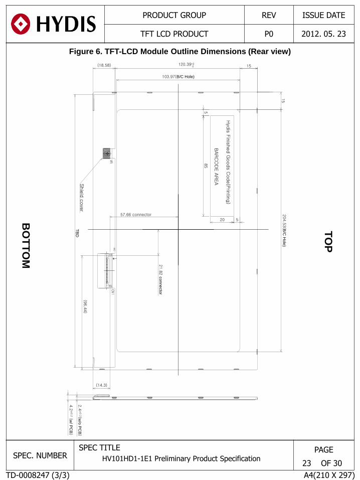
Figure 6. TFT-LCD Module Outline Dimensions (Rear view)
TO
P
BO
TT
OM
(18.58) 120.39+2 0
103.97(B/C Hole)
2.4
±0.2(w
/o P
CB
)
4.2
±0.2 (w
/ PC
B)
15
204.5
3(B
/C H
ole
)
15
TB
D
21.8
2 c
on
ne
cto
r
57.66 connector
Shie
ld c
over
(14.3)
(96.4
4)
1
Hydis
Fin
ished G
oods C
ode(P
rintin
g)
BAR
CO
DE A
REA
85
5
20 5

TD-0008247 (3/3) A4(210 X 297)
PRODUCT GROUP REV ISSUE DATE
TFT LCD PRODUCT P0 2012. 05. 23
SPEC. NUMBER SPEC TITLE
HV101HD1-1E1 Preliminary Product Specification PAGE
OF 30 24
12.0 RELIABLITY TEST The Reliability test items and its conditions are shown in below.
< Table10, Reliability Test >
No Test Item Test Condition Operating
1 High temperature storage test
Ta = 60 C, 240 hrs No
2 Low temperature storage test
Ta = -20 C, 240 hrs No
3 High temperature & high humidity operation test
Ta = 50 ℃, 80%RH, 240hrs Yes
4 High temperature operation test
Ta = 50 C, 240 hrs Yes
5 Low temperature operation test
Ta = 0 C, 240 hrs Yes
6 Thermal shock Ta = -20 C 60 C (30 min), 100 cycle No
7 Vibration test (non-operating)
Frequency : 10~500Hz Gravity/AMP : 1.5G Period : X,Y,Z 30min
NO
8 Shock test (non-operating)
Gravity : 220G Pulse width : 2ms, half sine wave ±X, ±Y, ±Z Once for each direction
No
9 Electro-static discharge test (non-operating)
C=150pF, R=330Ω, 5cycle/
Air 15KV, Contact 8kV No
Note 1
Note 1 :
1. ESD test condition is standard of customer system.

TD-0008247 (3/3) A4(210 X 297)
PRODUCT GROUP REV ISSUE DATE
TFT LCD PRODUCT P0 2012. 05. 23
SPEC. NUMBER SPEC TITLE
HV101HD1-1E1 Preliminary Product Specification PAGE
OF 30 25
13.0 HANDLING & CAUTIONS
13.1 Cautions when taking out the module
Pick the pouch only, when taking out module from a shipping package.
13.2 Cautions for handling the module
As the electrostatic discharges may break the LCD module, handle the LCD module with
care. Peel a protection sheet off from the LCD panel surface as slowly as possible.
As the LCD panel and back - light element are made from fragile glass (epoxy) material,
impulse and pressure to the LCD module should be avoided.
As the surface of the polarizer is very soft and easily scratched, use a soft dry cloth
without chemicals for cleaning.
Do not pull the interface connector in or out while the LCD module is operating.
Put the module display side down on a flat horizontal plane.
Handle connectors and cables with care.
13.3 Cautions for the operation
When the module is operating, do not lose MCLK, DE signals. If any one of these signals
were lost, the LCD panel would be damaged.
Obey the supply voltage sequence. If wrong sequence is applied, the module would be
damaged.
13.4 Cautions for the atmosphere
Dew drop atmosphere should be avoided.
Do not store and/or operate the LCD module in a high temperature and/or humidity
atmosphere. Storage in an electro-conductive polymer packing pouch and under relatively
low temperature atmosphere is recommended.
13.5 Cautions for the module characteristics
Do not apply fixed pattern data signal to the LCD module at product aging.
Applying fixed pattern for a long time may cause image sticking.
13.6 Cautions for the digitizer assembly
When assembling FPC connector, do not flip connector past 90° due to possible damage
to connector.
When positioning digitizer underneath driver IC, do not lift driver IC past 90° due to
possible damage to drive IC pattern.
Please be warned that during assembly of digitizer, the opening or closing of FPC will
result in possible electrostatic discharge damage to the LED
13.7 Other cautions
Do not re-adjust variable resistor or switch etc.
When returning the module for repair or etc., Please pack the module not to be broken.
We recommend to use the original shipping packages.

TD-0008247 (3/3) A4(210 X 297)
PRODUCT GROUP REV ISSUE DATE
TFT LCD PRODUCT P0 2012. 05. 23
SPEC. NUMBER SPEC TITLE
HV101HD1-1E1 Preliminary Product Specification PAGE
OF 30 26
14.0 LABELS
14.1 Product Label
Printing at Reflection sheet (LCM back side)
Model : HV101HD1-1E1
R H V 1 0 1 H D 0 0 0 2 1 2 0 1 0 4
Output
Factory
R : T2
U : WJ LCM1
V : WJ LCM2
Hydis model name BOM number Serial number
Year
2012 : 2
2013 : 3
Week
1

TD-0008247 (3/3) A4(210 X 297)
PRODUCT GROUP REV ISSUE DATE
TFT LCD PRODUCT P0 2012. 05. 23
SPEC. NUMBER SPEC TITLE
HV101HD1-1E1 Preliminary Product Specification PAGE
OF 30 27
14.2 Packing Label

TD-0008247 (3/3) A4(210 X 297)
PRODUCT GROUP REV ISSUE DATE
TFT LCD PRODUCT P0 2012. 05. 23
SPEC. NUMBER SPEC TITLE
HV101HD1-1E1 Preliminary Product Specification PAGE
OF 30 28
15.0 PACKING INFORMATION 15.1 Packing order
Notes : 1. Box Dimension: TBD 2. Package Quantity in one Box : TBD

TD-0008247 (3/3) A4(210 X 297)
PRODUCT GROUP REV ISSUE DATE
TFT LCD PRODUCT P0 2012. 05. 23
SPEC. NUMBER SPEC TITLE
HV101HD1-1E1 Preliminary Product Specification PAGE
OF 30 29
15.2 Pallet Packing
* Note
Pallet Dimension : TBD
Package Quantity in one Box : TBD
Box Quantity in one Pallet : TBD


![Lung Protective Mechanical Ventilation · Summary 0.38 [0.20 ... 13 –16 kPa 21.4 14.4 ± 0.9 0.4 [0.4 –0.42] 5 [5 –10] > 16 kPa 22.3 20.7 ± 6.0 0.4 [0.4 –0.45] 5 [5 –10]](https://static.fdocuments.in/doc/165x107/5f6ae5a024d48931f51ed82b/lung-protective-mechanical-ventilation-summary-038-020-13-a16-kpa-214.jpg)


![· 4.1.4035 0.4 0.-4.*..4 1.4 0.4 4.j 1.4 0.4 14-7.5 , 4] 1.4 . 4 30 )1428 ... 04 , , 4i.4J..ž dJ 04 : 04 I -i 0.4 0.4 pl...i4 4.41 k...l.Ä.; [4]](https://static.fdocuments.in/doc/165x107/5e12b7c12d278479c65ce711/414035-04-0-44-14-04-4j-14-04-14-75-4-14-4-30-1428-04-.jpg)

