
Title: font: times; size: 18 point; style: plain ...doras.dcu.ie/17972/1/OpEx_submission.doc ·...
23
Method to improve the noise figure and saturation power in multi- contact semiconductor optical amplifiers: simulation and experiment Kevin Carney, 1,* Robert Lennox, 2 Ramon Maldonado-Basilio 1 , Severine Philippe 1 , Frederic Surre 1 , Louise Bradley 2 and Pascal Landais 1 1 The Rince Institute, School of Electronic Engineering, Dublin City University, Glasnevin, Dublin 9, Ireland 2 School of Physics, Trinity College Dublin, Dublin 2, Ireland * [email protected] Abstract: The consequences of tailoring the longitudinal carrier density along the active layer of a multi-contact bulk semiconductor optical amplifier (SOA) are investigated using a rate equation model. It is shown that both the noise figure and output power saturation can be optimized for a fixed total injected bias current. The simulation results are validated by comparison with experiment using a multi-contact SOA. The inter- contact resistance is increased using a focused ion beam in order to optimize the carrier density control. A chip noise figure of 3.8 dB and a saturation output power of 9 dBm are measured experimentally for a total bias current of 150 mA. 2012 Optical Society of America OCIS codes: (250.9580) Semiconductor optical amplifiers; (060.4510) Optical communications. References and links 1. J. Mørk, M. L. Nielsen, T. W. Berg, “The Dynamics of Semiconductor Optical Amplifiers: Modeling and Applications”, Optics and Photonics News 14, 42-48 (2003). 2. Y. Liu, E. Tangdiongga, Z. Li, H. de Waardt, A. M. J. Koonen, G. D. Khoe, X. Shu, I. Bennion, and H. J. S. Dorren, “Error Free 320Gb/s All-Optical Wavelength Conversion using a Single Semiconductor Optical Amplifier”, J. Lightw. Technol. 25, 103-108 (2007).
Transcript of Title: font: times; size: 18 point; style: plain ...doras.dcu.ie/17972/1/OpEx_submission.doc ·...
Method to improve the noise figure and saturation power in multi-contact semiconductor
optical amplifiers: simulation and experimentKevin Carney,1,* Robert Lennox,2 Ramon Maldonado-Basilio1, Severine Philippe1,
Frederic Surre1, Louise Bradley2 and Pascal Landais1
1The Rince Institute, School of Electronic Engineering, Dublin City University, Glasnevin, Dublin 9, Ireland2School of Physics, Trinity College Dublin, Dublin 2, Ireland
Abstract: The consequences of tailoring the longitudinal carrier density along the active layer of a multi-contact bulk semiconductor optical amplifier (SOA) are investigated using a rate equation model. It is shown that both the noise figure and output power saturation can be optimized for a fixed total injected bias current. The simulation results are validated by comparison with experiment using a multi-contact SOA. The inter-contact resistance is increased using a focused ion beam in order to optimize the carrier density control. A chip noise figure of 3.8 dB and a saturation output power of 9 dBm are measured experimentally for a total bias current of 150 mA. 2012 Optical Society of America OCIS codes: (250.9580) Semiconductor optical amplifiers; (060.4510) Optical communications.
References and links1. J. Mørk, M. L. Nielsen, T. W. Berg, “The Dynamics of Semiconductor Optical Amplifiers: Modeling and Applications”, Optics and Photonics News 14, 42-48 (2003).2. Y. Liu, E. Tangdiongga, Z. Li, H. de Waardt, A. M. J. Koonen, G. D. Khoe, X. Shu, I. Bennion, and H. J. S. Dorren, “Error Free 320Gb/s All-Optical Wavelength Conversion using a Single Semiconductor Optical Amplifier”, J. Lightw. Technol. 25, 103-108 (2007).3. A. Borghesani, “Semiconductor Optical Amplifiers for Advanced Optical Applications”, in Proc. International Conference on Transparent Optical Networks 2006, (Nottingham, UK, 2006) pp. 119-122.4. L.H. Spiekman, “Ubiquitous Amplification: Applications of the Semiconductor Optical Amplifier”, in Proc. COIN-NGNCON 2006, (Jeju, South Korea, 2006), pp. 292-294.5. D.F. Welch, “Large-Scale InP Photonic Integrated Circuits: Enabling Efficient Scaling of Optical Transport Networks”, IEEE J. Sel. Topics Quantum Electron. 13 22-31 (2007).6. H. Kim and J. Song, "All-optical frequency downconversion technique utilizing a four-wave mixing effect in a single semiconductor optical amplifier for wavelength division multiplexing radio-over-fiber applications," Opt. Express 20, 8047-8054 (2012).7. R. Bonk, G. Huber, T. Vallaitis, S. Koenig, R. Schmogrow, D. Hillerkuss, R. Brenot, F. Lelarge, G. Duan, S. Sygletos, C. Koos, W. Freude, and J. Leuthold, "Linear semiconductor optical amplifiers for amplification of advanced modulation formats," Opt. Express 20, 9657-9672 (2012).8. F. Crottini, P. Salleras, M. A. Moreno, B. Dupertuis, B. Deveaud, and R. Brenot, “Noise Figure Improvement in Semiconductor Optical Amplifiers by Holding Beam at Transparency Scheme”, IEEE Photon. Technol. Lett., 17 977-979 (2005).9. R. Brenot, F. Pommereau, O. Le Gouezigou, J. Landreau, F. Poinet, and L. Le Gouezigou, “Experimental Study of the Impact of Optical Confinement on Saturation Effects in SOA”, in Proc. Optical Fiber Communications Conference, (Anaheim, Calif., 2005). 10. E.S. Bjorlin, J.E. Bowers, “Noise Figure of Vertial-Cavity Semiconductor Optical Amplifiers”, IEEE J. Quantum Electron. 38 61-66 (2002).11. K. Morito, S, Tanaka, S. Tomabechi, A. Kuramata, “A Broadband MQW Semiconductor Optical Amplifier with High Saturation Output Power and Low Noise Figure”, IEEE Photon. Technol. Lett. 17 974-976 (2005).
12. K. Carney, R. Lennox, R. Maldonado-Basilio, S. Philippe, A.L. Bradley, P. Landais, “Noise Controlled Semiconductor Optical Amplifier based on Lateral Cavity Laser”, Electronics Letters 46 1288-1289 (2010).13. G. Bendelli, K . Komori, S. Arai, and Y. Suematsu, “A New Structure for High-Power TW-SLA”, IEEE Photon. Technol. Lett. 3 42 (1991). 14. G. Guiliani, and D. D’Alessandro. “Noise analysis of conventional and gain-clamped semiconductor optical amplifiers”, J. Lightw. Technol. 18 1256 (2000).15. M. Yoshino and K. Inoue, “Improvement of saturation power in a semiconductor laser amplifier through pumping light injection”, IEEE Photon. Technol. Lett. 8 58-59 (1996).16. S. S. Saini, J. Bowser, R. Enke, V, Luciani, P. J. S. Heim, and M. Dagenais. “A semiconductor optical amplifier with high saturation power, low noise figure and low polarization dependent gain over the C-band”, in Proc. Lasers and Electro-Optics Society, (Rio Grande, Puerto Rico, 2004) pp. 102-103.17. R. Lennox, K. Carney, R. Maldonado-Basilio, S. Philippe, A.L. Bradley, P. Landais, “Impact of Bias Current Distribution on the Noise Figure and Saturation Power of a Multi-Contact Semiconductor Optical Amplifier”, Opt. Lett. 36 2521-2523 (2011).18. T. Mukai and Y. Yamamoto, “Noise in an AlGaAs Semiconductor Laser Amplifier”, IEEE J. Quantum Electron. 18 564-575 (1982).19. E. Desurvire, “On the Physical Origin of the 3dB Noise Figure Limit in Laser and Parametric Optical Amplifiers”, Opt. Fiber Technol. 5 40-61 (1999).20. M. Shtaif, B. Tromborg, G. Eisenstein, “Noise spectra of Semiconductor Optical Amplifiers: Relation between Semiclassical and Quantum Descriptions”, IEEE J. Quantum Electron. 34 869-878 (1998).21. H.A. Haus, “The Noise Figure of Optical Amplifiers”, IEEE Photon. Technol. Lett. 10 1602-1604 (1998).22. T. Briant, P. Grangier, R. Tualle-Brouri, A. Bellemain, R. Brenot, B. Thedrez, “Accurate Determination of the Noise Figure of Polarization Dependent Optical Amplifiers: Theory and Experiment”, J. Lightw. Technol. 24 1499-1503 (2006).23. D.M. Baney, P. Gallion, R. S. Tucker, “Theory and Measurement Techniques for the Noise Figure of Optical Amplifiers”, Opt. Fiber Technol. 6 122-154 (2000).24. Connolly MJ, Semiconductor Optical Amplifiers, (Kluwer Academic Publishers, 2002).25. Cristiano Gallep, Andrés Rieznik, Hugo Fragnito, Newton Frateschi, and Evandro Conforti, "Black-box model for the complete characterization of the spectral gain and noise in semiconductor optical amplifiers," Opt. Express 14, 1626-1631 (2006).26. Jongwoon Park and Yoichi Kawakami, "Time-domain models for the performance simulation of semiconductor optical amplifiers," Opt. Express 14, 2956-2968 (2006).27. M.J. Adams, J.V. Collins, I.D. Henning, “Analysis of Semiconductor Laser Optical Amplifiers”, IEE Proceedings J Optoelectronics 132 58-63 (1985).28. T. Durhuus, B. Mikkelsen, K.E. Stubkjaer, “Detailed Dynamic Model for Semiconductor Optical Amplifiers and their Crosstalk and Intermodulation Distortion”, J. Lightw. Technol 10 1056-1069 (1992).29. M.J. Connolly, “Wideband Semiconductor Optical Amplifier Steady-State Numerical Model”, IEEE J. Quantum Electron. 37 439-447 (2001).30. H.T. Friis, “Noise Figures of Radio Receivers”, Proc. of the IRE 32 419-422 (1944).31. Y. Yamamoto, K. Inoue, “Noise in Amplifiers”, J. Lightw. Technol. 21 2895-2915 (2003). 32. F. Surre and P. Landais, “A semiconductor optical amplifier with a reduced noise figure,” UK patent GB0821602.0, Feb. 9, 2011.
1. Introduction
The potential of semiconductor optical amplifiers (SOA) as non-linear entities within optical communication systems has resulted in a surge in experimental and theoretical investigations over the last two decades [1]. SOAs have garnered interest as candidates to replace current electrical methods of signal processing within optical networks, with the capacity to work at bit rates of 320Gb/s [2]. The benefits when operated in saturation have also been demonstrated as high speed wavelength converters and remote modulators [3-5]. In addition SOA present economic advantages, particularly pertaining to fabrication, low power consumption and suitability for integrated photonics [6]
Despite these attractive features, the role of SOAs in linear amplification systems is limited. While there is some use of SOAs in such applications [7], the Erbium doped fiber amplifier (EDFA) is the commonly chosen option. One of the major limitations of SOAs as linear

components is a high noise figure (NF). To date, a number of methods for NF reduction have been proposed. An improvement in steady state NF was realised through optical injection of a holding beam in both co- and counter-propagation geometries, essentially resulting in a modification of the carrier density profile [8]. More recent works include alterations to the confinement factor [9], vertical cavity SOAs (which have the added advantage of low modal loss) [10], and various device structures ranging from unique waveguide termination to low internal loss structures [11]. The use of a lateral lasing cavity to clamp a portion of the SOA waveguide, in order to shape the carrier density profile, has also been considered [12]. The results of many of these methods have been largely positive in terms of NF but have presented other disadvantages. For example, solutions involving a holding beam necessitate additional equipment and expense. Reducing the confinement factor to decrease NF also decreases the optical gain, and vertical-cavity SOAs suffer from a limited gain bandwidth due to the use of a resonant cavity.
An additional drawback of SOAs is that the saturation output power (P sat) can be low, limiting the dynamic range of input powers over which the signals can be amplified cleanly without distortion. This can be a significant penalty when the SOA is being used as a multichannel amplifier, due to the effects of channel crosstalk. As with the NF, researchers have investigated ways to increase Psat such that the range of operation is increased without undermining other device characteristics. Techniques to increase saturation output power include reducing the confinement factor [9], the use of flared waveguides [13], gain clamping [14], pump beams [15] and varying the contact resistance in order to increase the current density along the waveguide [16]. These techniques have various disadvantages, such as reduced gain when reducing the confinement factor, increased cost of fabrication for gain clamped devices and, similar to attempts to reduce the NF, the additional cost and system complexities associated with pump beam schemes.
Previously, it was experimentally demonstrated that varying the carrier density profile in a multi-contact SOA could influence the chip-NF and Psat [17]. The focus of this paper is to present a rate equation model for the numerical investigation of the physics underlying this phenomenon. Simulation results for different carrier density profiles are discussed. It will be shown that the carrier density profile can be tailored to minimize the chip NF or to optimize Psat for a fixed total bias current. The model is validated by comparison with experimental results obtained using a multi-contact bulk SOA. Additionally, it is shown that good control of the inter-contact resistance is important in order to realize the potential for NF reduction. The inter-contact resistance of the fabricated devices is increased using a Focused Ion Beam (FIB) technique and yields closer agreement between the experimental and simulation results.
2. Noise figure and power saturation
2.1 Noise figure
As a signal is amplified it experiences degradation due to additive noise, an unavoidable consequence of spontaneous emission. The fundamental limits on information systems are governed by this noise, and so mitigation is of the utmost importance. Many publications have dealt with the theoretical determination of optical noise and its origins in great detail [18-23]. A widely accepted definition exists to facilitate consistent measurement in the laboratory [23].
The noise is quantified in the optical and electronic domains by the NF, defined as the degradation of the signal-to-noise ratio (SNR) of a signal by propagation through active and passive elements. In linear units this is expressed as,
(1)
where SNRin and SNRout represent the SNR of the input and output signals, respectively. For clarity, when nf is given in lower case, it is calculated in linear scale, and in upper case, NF,
denotes a decibel (dB) scale. The resultant NF formula, which takes into account the dominant individual sources of noise, is given in terms of experimentally obtained optical parameters [23],
(2)
The first term in parenthesis represents the noise associated with beating between the signal and the co-polarised amplified spontaneous emission (ASE) within the measurement bandwidth where G is the single pass gain, ν is the optical frequency of the injected signal, and ρASE is the ASE power spectral density within this bandwidth. This is the dominant source of noise in SOAs of high gain. The second term in brackets relates to the shot noise of the signal itself. For appreciable gain the latter may be neglected, as the shot noise is relatively insignificant at higher signal powers.
2.2 Saturation output power
As the signal power injected into an SOA is increased, or as amplified spontaneous emission increases with gain, the carriers in the active region used for amplification are depleted, causing the gain to decrease. The saturation output power is defined as the output power emitted by the SOA at the point at which the gain has reduced by 3dB. The saturation output power is given by [24],
(3)
where A is active region area in the plane perpendicular to propagation, Γ confinement factor, and the saturation intensity Isat is given by,
(4)
In this equation a1 is differential gain coefficient, the variation of gain with respect to the carrier density, ν is the signal frequency and τ is spontaneous carrier lifetime. Thus a decrease in confinement factor or spontaneous carrier lifetime or an increase in waveguide area can give rise to an increased saturation power [9]. These approaches are not incompatible with our solution, which is described below.
3. Simulation
3.1 Structure of simulation
A variety of approaches to modelling SOAs is found in the literature [25, 26]. The simulation tool presented herein has been developed based on a travelling wave model [27, 28]. The SOA is modelled in n subsections, each of them electrically isolated from its neighbours. The values for all variables are calculated in each subsection. The carrier density is set at an initial value and is updated from the determined values of the ASE and signal fields. This process continues over a defined number of iterations. Values for carrier density as well as ASE and signal fields are used as initial conditions for the next iteration.
The model has been developed to investigate the effects of tailoring the longitudinal carrier density and see how it may provide control of the NF and power saturation. The noise model used in the simulation is a deterministic model. In this case the level of ASE is determined for the signal wavelength only, using the material gain approximation from reference 27. This noise model is less accurate for very low input powers, where the effect of wide-band ASE on the carrier density is proportionally greater. However, the powers used in the simulation study are appropriate to the deterministic model, and as will be shown there is good agreement
between the trends of the experimental data and the measurements. Furthermore, the model considers the ideal case in which the carrier density profile is determined by the injected bias current only, in which case each sub-section is perfectly isolated and carrier diffusion is not taken into account.
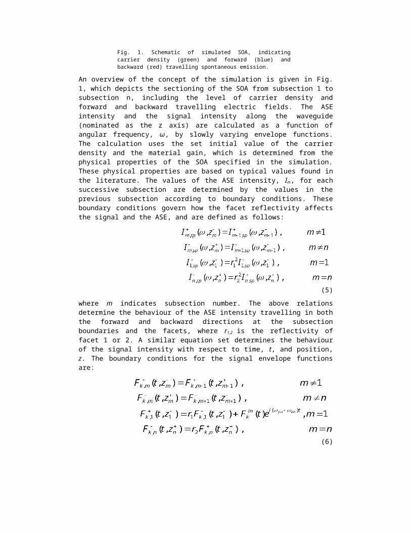
Fig. 1. Schematic of simulated SOA, indicating carrier density (green) and forward (blue) and backward (red) travelling spontaneous emission.
An overview of the concept of the simulation is given in Fig. 1, which depicts the sectioning of the SOA from subsection 1 to subsection n, including the level of carrier density and forward and backward travelling electric fields. The ASE intensity and the signal intensity along the waveguide (nominated as the z axis) are calculated as a function of angular frequency, ω, by slowly varying envelope functions. The calculation uses the set initial value of the carrier density and the material gain, which is determined from the physical properties of the SOA specified in the simulation. These physical properties are based on typical values found in the literature. The values of the ASE intensity, Im, for each successive subsection are determined by the values in the previous subsection according to boundary conditions. These boundary conditions govern how the facet reflectivity affects the signal and the ASE, and are defined as follows:
(5)
where m indicates subsection number. The above relations determine the behaviour of the ASE intensity travelling in both the forward and backward directions at the subsection boundaries and the facets, where r1,2 is the reflectivity of facet 1 or 2. A similar equation set determines the behaviour of the signal intensity with respect to time, t, and position, z. The boundary conditions for the signal envelope functions are:
(6)
where ωp0 and ωk0 are the gain peak angular frequency and signal angular frequency, respectively. Using the values for the ASE envelope function, modified by the boundary conditions above, the spontaneous emission photon density is obtained:
(7)
where Nm is the carrier density in subsection m, Gm is the single pass gain (expressed in linear scale) in subsection m calculated from the carrier density and material gain [27], Rr(Nm) is the radiative recombination rate, α is the internal loss coefficient and β is the effective spontaneous emission factor, a measure of the spontaneous emission coupled to the traveling mode. The photon density for the signal is also obtained in a similar way using the signal envelope function:
(8)
The values for the spontaneous emission photon density and the signal photon density are then used to solve the carrier density rate equation:
(9)
where im is the bias current injected at an individual subsection m, q is the charge of the carriers and V is the volume of the active region in subsection m. R(Nm) represents the recombination rates equal to ANm+BNm
2+CNm3, where A is the non-radiative recombination
coefficient, B the radiative recombination coefficient, and C the Auger recombination coefficient. This entire process comprises a single iteration of the model. The solved value of the carrier density is used to calculate the ASE and signal fields for the next iteration. Once convergence is reached, the gain and the NF are then obtained. The NF of each subsection in the SOA is determined from the population inversion factor, nsp, which is integral to the concept of reducing the NF, as detailed below.
3.2 Calculation of the noise figure from carrier density
The NF is, in general, proportional to the population inversion factor nsp, which is defined as,
(10)
where γ and α represent the stimulated emission and absorption rates, respectively. These values are dependent on the level of carrier density in the SOA. Thus expressing the optical NF formula (2) in terms of nsp, allows for the qualitative argument that increasing the conduction band population level has the effect of decreasing the NF. The equation for the additive noise power of an amplifier is given by,
(11)
where B0 is the measurement bandwidth and G is the single pass chip gain. As ρASE is equal to the noise power per unit bandwidth, Eq. (11) can be re-written as,
(12)
Replacing ρASE in Eq. (2) with (12) yields an expression for the noise figure in terms of nsp and gain, expressed in linear units,
(13)
For the situation where G >> 1, this expression reduces to nf = 2nsp, which, in the case of total population inversion (nsp = 1), leads to a quantum limit of the NF of 3dB [19].
3.3 Reduction of noise figure
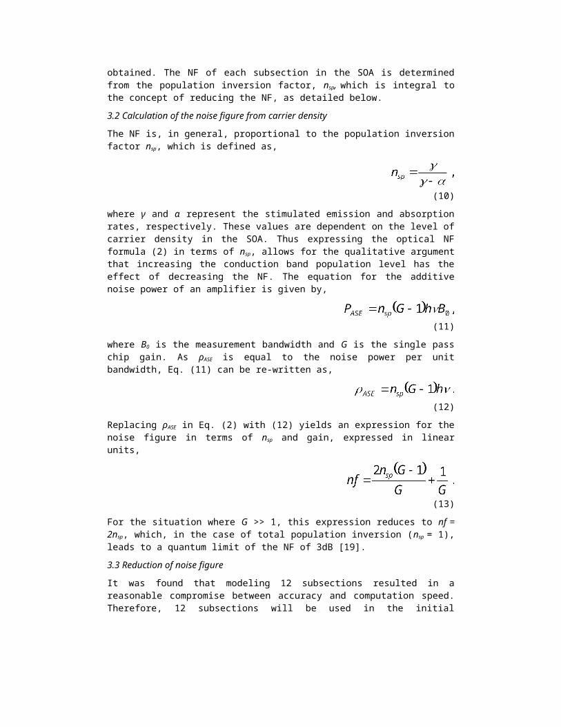
It was found that modeling 12 subsections resulted in a reasonable compromise between accuracy and computation speed. Therefore, 12 subsections will be used in the initial investigation of the potential to control the SOA NF and power saturation by tailoring the carrier density profile. A higher number of subsections will be used subsequently to achieve greater accuracy for direct comparison with experimental results. In Fig. 2 the carrier density and the population inversion are presented as a function of subsection. The dependence of the inversion factor on the carrier density can clearly be seen.
Fig. 2. Simulated carrier density and inversion factor dependence along the length of the device, for two opposite longitudinal carrier density profiles.
This dependence explains why increasing carrier density reduces the NF. However we cannot simply pump the device indefinitely for an improved NF due to the effects of ASE saturation and Auger recombination at higher biases. Therefore, for a given overall bias current itot, it is proposed to reduce the total NF (NFtot) with a very specific carrier density profile, compared with the carrier density profile for a standard SOA.
To control the NF at itot, the carrier density at the designated input of the device is held at a high value, increasing the gain and lowering the NF at this point. Backward travelling ASE cannot be neglected as it consumes carriers at the input of the device, which would otherwise available for signal gain, and so this effect must be reduced. A low carrier density is created in the output end of the device to satisfy this requirement. This is the carrier density profile shown at the top of Fig. 2 (profile 1). In profile 2, at the bottom of Fig. 2, the carrier density is low at the input and high at the output of the device. To explain the effect on NFtot in profile 1, one can think of the SOA as a chain of individual amplifiers, equivalent to the subsections in the simulation. The overall NF of such a system is largely determined by the NF of the initial subsections, as shown in [30] for an electrical amplifier cascade, and more recently optically in [31]. The Friis equation illustrates this idea,
(14)
where nfm and gm are the NF and gain, respectively, of a particular subsection m. Each successive term in the equation is reduced in value compared with the last, due to the presence of an additional gain term at every stage. The NF is added to cumulatively by each successive element in the equation, which are reducing in magnitude. Thus the first few terms make the most significant contribution to the overall value of nftot. This principle is illustrated further by Fig. 3(a) below. Under the same itot, the contribution of each subsection to the increase in overall NF (in dB) for three different distributions of carrier density, profiles 1 and 2, as well as profile from a standard SOA. Compared with both the standard profile and profile 2, the increase in NF for profile 1 in the initial subsections is smaller. This falls in line with what we expect based on Eq. (14), in so far as we try to minimize the input NF. In addition, while the increase in NF for this profile in the final subsections will be larger than the other cases, the magnitude is relatively insignificant, and so cannot be resolved in this figure. It should be noted that this figure represents the cumulative addition of NF to the initial NF of the first modeled subsection. The individual NF of this subsection is below the quantum limit of 3dB in each bias configuration. This anomaly is explained due to the sectioning of the model. If this particular section was examined on its own, it would itself have to be sectioned in order to accurately determine the NF, which would then be greater than 3dB. The above scenarios illustrate the concept by comparing three extreme examples.
From this comparison it is clear that to achieve the lowest NFtot, the subsections at the input of the device must be maintained at high carrier density. A three contact device is simulated by a model with 12 subsections. A total of 80 mA is injected into the first 4 subsections (20 mA per subsection), representing the first contact, and the bias applied to the middle and output contacts is varied from 0 - 90mA. The NF values are plotted below in Fig. 3(b). With a high bias injected into the first simulated contact there is an evolution of the NF reduction as the middle contact is increased and the output bias held constant below 30 mA. As predicted previously, the NF is expected to decrease from its maximum value, for lower middle and output biases, to its minimum for a carrier profile approaching that of profile 1. The increase in NF in the upper-right portion of the graph compared with the upper-left portion indicates that the NF cannot be minimized by arbitrarily pumping the SOA, and that therefore, for a specific total bias current, a specific carrier density profile exists where the NF is optimized.
Fig. 3. (a) Graphical illustration of the Friis equation for three separate bias configurations depicting the increase in NF for each successive subsection. Also indicated are the initial subsection NF and final NF values, illustrating the extent of NF increase at each bias configuration; (b) NF as a function of bias current applied to the middle and end contact of a simulated three contact SOA. The first contact is biased at 80 mA, for 1570 nm at for an injected signal of –20 dBm.
2 3 4 5 6 7 8 9 10 11 12
0.0
0.2
0.4
0.6
0.8
1.0
1.2
1.4
Incre
ase
in NF
, dB
Contributing subsection
Profile 1 Standard Profile 2
Profile 1 Standard Profile 2Subsection 1 NF (dB)
Final NF (dB)2.35 2.18 2.094.47 5.05 7.19
(a)
3.4 Controlling saturation power
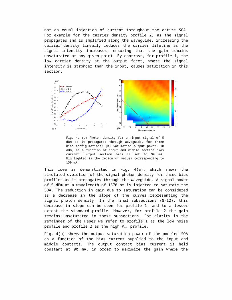
In contrast to the conditions for reduced NF, in order to increase the saturation output power of the SOA the current density in the device must be increased. The reason for this lies in the fact that the saturation power is inversely proportional to the spontaneous carrier lifetime, which in turn is inversely proportional to the carrier density (see Eq. 4). Thus operating at a higher bias current will increase Psat. This also has the effect of increasing the ASE, which causes a decrease in the stimulated emission lifetime, further increasing the saturation power. However, for a fixed total bias current, the most efficient distribution of carriers is not an equal injection of current throughout the entire SOA. For example for the carrier density profile 2, as the signal propagates and is amplified along the waveguide, increasing the carrier density linearly reduces the carrier lifetime as the signal intensity increases, ensuring that the gain remains unsaturated at any given point. By contrast, for profile 1, the low carrier density at the output facet, where the signal intensity is stronger than the input, causes saturation in this section.
Fig. 4. (a) Photon density for an input signal of 5 dBm as it propagates through waveguide, for three bias configurations; (b) Saturation output power, in dBm, as a function of input and middle section bias current. Output section bias is set to 90 mA. Highlighted is the region of values corresponding to 150 mA.
This idea is demonstrated in Fig. 4(a), which shows the simulated evolution of the signal photon density for three bias profiles as it propagates through the waveguide. A signal power of 5 dBm at a wavelength of 1570 nm is injected to saturate the SOA. The reduction in gain due to saturation can be considered as a decrease in the slope of the curves representing the signal photon density. In the final subsections (8-12), this decrease in slope can be seen for profile 1, and to a lesser extent the standard profile. However, for profile 2 the gain remains unsaturated in these subsections. For clarity in the remainder of the Paper we refer to profile 1 as the low noise profile and profile 2 as the high Psat profile.
Fig. 4(b) shows the output saturation power of the modeled SOA as a function of the bias current supplied to the input and middle contacts. The output contact bias current is held constant at 90 mA, in order to maximize the gain where the signal is strongest. As expected, the value for Psat increases with the total bias current, reaching a maximum value of ~ 16 dBm when all contacts are biased at 90 mA. The red line highlights the Psat values for a total bias current of 150 mA. This value has been selected as it corresponds to the manufacturer imposed limit for the test multi-contact SOAs, due to temperature restrictions. Within this limit, the highest Psat value is obtained with an input section current of 10 mA and a middle section current of 50 mA. Fig. 5 shows the simulated gain, NF and saturation power values for various bias conditions modeled for an SOA with three contacts. The middle contact bias is held constant whilst the two facet contacts are varied. This represents a transition from the low noise to high Psat profiles for a constant total injected bias. A signal with a power of -15
0 2 4 6 8 10 120.20.30.40.50.6
0.70.80.9
1.01.1
1.21.31.4
Standard Profile 1 Profile 2
Sign
al Ph
oton D
ensit
y, m
-3
Subsection
x1021
(a)
dBm at 1570 nm is injected. The maximum gain is observed while operating in the standard condition, with equal current injection to all contacts, corresponding to a single contact SOA. The magnitude of the gain decreases as the carrier density profile becomes less symmetrical. As expected, the NF is observed to decrease as the bias condition approaches that of the previously discussed low noise profile, and the saturation power increases for the opposite bias distribution, like that shown as the high Psat profile. It is observed that the NF is varies over a range of 2.72 dB, while the saturation output power has a range of 4.21dB. Therefore, it is noted that controlling the carrier density profile has a larger impact on the power saturation than on the NF.
Fig. 5. Simulated gain, noise figure and saturation power for various bias configurations. The overall bias current is 150mA.
4. Comparison with experimental results
The experimentally characterized multi-contact SOA studied in this paper is 700 μm long and has three contacts. After fabrication there is a slight variation in the size of the contacts. The basic gain and NF characteristics of the SOA are modeled using a 24 subsection simulation, for a range of wavelengths and input powers. In order to more accurately represent the actual contact sizes of the SOA, 8 of these subsections are representative of the input contact, 9 subsections for the middle contact and 7 subsections for the end contact. For the low noise profile, 80 mA is injected at the input contact, 50 mA in the middle contact and 20 mA in the output contact, and vice-versa for the high Psat case. The standard SOA case is modeled by injecting 50 mA into each contact. The total bias for all three cases is limited to 150 mA. These dimensions and current limitation are determined by the prototypes devices.
Fig. 6. Simulated evolution of ASE intensity along waveguide for both forward (solid) and backward (dash) traveling ASE, for the standard, low noise and high Psat cases
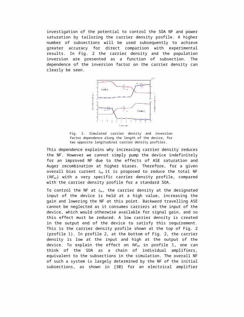
Fig. 6 shows the modeled distribution of the ASE intensity along the waveguide in both forward and reverse directions, for the three relevant bias configurations. Of particular note is the reduction of ASE for both high saturation power and low noise bias cases. This phenomenon is due to reduced amplification of spontaneous emission in regions of low current density, reducing ASE at the facets.
Fig. 7. (a) Simulated gain (dash) and noise figure (solid) spectra, for an input signal power of -15 dBm. The overall bias current of the SOA is 150 mA; (b) Gain (dash) as a function of the output power for the simulated device with an injected signal at 1570 nm. The overall bias current of these three SOAs is 150
mA.
The simulated gain and NF for an injected power of 15 dBm at various wavelengths are plotted in Fig. 7(a) for the three bias conditions. The minimum NF determined by the simulation is 4.47 dB at 1570 nm, for the low noise bias configuration. The maximum gain is observed in the standard bias configuration and is measured as 18.1 dB at a wavelength of 1555 nm. A gain difference of approximately 0.7 dB is observed between the low noise and high Psat cases. This discrepancy is explained by a slight difference in the size of the individual contacts of the SOA, which leads to different levels of carrier density per equivalent section for the low noise case vis-à-vis the high Psat case. A reduction in the NF of approximately 0.6 dB between the low noise configuration and the standard configuration is visible in the simulated data. Whereas a high current density at the input of the device leads to a lower NF, increasing the injected current along the length of the waveguide towards the output facet increases the saturation power of the device, allowing it to operate as a linear amplifier for a wider range of input powers. Fig. 7(b) shows the gain as a function of output power for the simulated device. The injected signal is at the peak gain wavelength for the low noise and high Psat profiles, which is 1570 nm for the simulation. An increase in saturation power of 1.72 dB, from 10.82 dBm to 12.53 dBm, is observed between the standard SOA case and the high saturation power case.
Based on the previous computational investigation, a multi-contact bulk SOA has been fabricated and tested. The concept of reducing the NF based on tailoring the carrier density profile has been previously demonstrated in a single contact SOA incorporating a lateral lasing cavity in order to control the carrier density distribution [12]. The multi-contact SOA configuration is cheaper to process and, as can be seen from the simulation results, offers the possibility to operate in different modes. In practice, one may employ numerous current sources to drive each contact independently, or use a single source in conjunction with a resistor network [32]. The device under test is a bulk InP/InGaAsP SOA, angled and anti-reflection coated, with a length of approximately 700 μm. Three electrodes are used for current injection into three sections of length 236 μm, 254 μm and 210 μm. Electrical isolation between the contacts is provided by a 10 μm slot, and resistance between sections is measured to be 300 Ω. For manufacturing reasons, the current in each contact is limited to 90 mA. A
1540 1550 1560 1570 1580 15904
6
8
10
12
14
16
18
4
6
8
10
12
14
16
18
Nois
e fig
ure,
dB
Gain,
dB
Wavelength, nm
Standard SOA Low noise High P sat
(a)-15 -10 -5 0 5 10 15
6
8
10
12
14
16
18
20
Gain,
dB
Output power, dBm
Standard SOA Low noise High P sat
(b)
schematic of the SOA is shown in Fig. 8. A preliminary experimental characterization of this device has been previously reported in [17]. In this section the experimental results provide validation of the modeling approach and, furthermore, comparison with the model also sheds further insight on some of the experimental observations.
Fig. 8. Schematic of multi-contact SOA, with three sections, driven by three separate current sources.
For the experimental characterization, the low noise profile consists of 90 mA injected at the input contact, 50 mA in the middle and 10 mA at the output contact, with the opposite injection scheme for the high Psat case. As for the simulation, the standard case consists of 50 mA injected to each contact. The reason for the difference in bias current in the simulated case is due to a difference in the transparency current in the low bias contact between the simulation and the actual device.
The gain and NF data are acquired using the optical NF formula (3), where the level of co-polarised ASE is measured using a linear polariser. Further details can be found in [17]. The gain and NF for an injected power of -15 dBm at various wavelengths are plotted in Fig. 9(a) for the three selected bias conditions. The minimum NF observed for the experimental data is 5.0 ± 0.2 dB at a wavelength of 1568 nm, measured for the low noise bias configuration. This compares favourably to NF values recorded for commercial SOAs. The corresponding minimum NF determined by the simulation is 4.5 ± 0.2 dB at 1570nm, for the low noise bias configuration. The maximum gain is again observed in the standard bias configuration and is measured as 17.5 ± 0.2 dB at a wavelength of 1563 nm. The gain difference of approximately 0.7dB observed between the low noise and high Psat cases in the simulated data is also present here. This discrepancy can been explained by a slight difference in the size of the individual sections of the SOA, as previously discussed. A reduction in the NF of approximately 0.3 dB between the low noise configuration and the standard configuration is visible, although this is not consistent across the entire bandwidth and is a smaller effect than anticipated. However, there is a clear reduction in the NF by approximately 2 dB at 1570 nm for the standard and low noise profiles compared with the high Psat profile. The trend of the experimental data is in agreement with the simulation data presented in Fig. 5.
Fig. 9. (a) Measured gain (square) and noise figure (triangles) spectra for SOA under investigation, for an input signal of -15 dBm; (b) Gain vs output power at 1570 nm injected wavelength.
In Fig. 5 it can be clearly seen that the slope of the NF versus bias configuration over the range from the low noise profile to the standard profile is relatively flat, whereas the NF is more sensitive to the change in bias over the range from the standard profile to high Psat
profile. Furthermore, Fig. 9(b) shows the gain as a function of output power for the three aforementioned bias configurations. The injected signal is at the measured peak gain wavelength of 1568 nm. A saturation power of 9 dBm is measured for the high P sat bias case. This represents a 1.5 dB increase over the standard case and 3 dB increase over the low NF case. This result corroborates the trend seen in the simulations. Fig. 5 clearly shows that Psat is sensitive to the changes in the bias configuration over the full range of bias profiles and that a similar level of change in Psat is expected as the profile is varied from the low noise case to the standard case and from the standard profile to the high P sat profile. The experimental results validate the modeling approach and present an excellent match with the simulation results presented in Fig. 7.
It is noted however that the simulation predicts a greater reduction of the NF of 0.6 dB relative to the standard case. It is considered that the lessening of the effect in the experimental device maybe due to carrier leakage across the sections. This would broaden the carrier profile, and impair the noise reduction effect. As previously discussed the simulation considered full isolation between sections and no carrier diffusion was taken into account, To explore further whether improved control of the carrier density profile can produced a further reduction in the NF relative to the standard profile, it was attempted to increase resistance between adjacent contacts using a Focused Ion Beam technique. The results are presented in Section 5.
4. FIB experiment
As discussed above, diffusion of carriers between the sections of the SOA could reduce the effectiveness of the injected bias current profile. Using a focused ion beam (FIB) technique, the resistance between the electrical contacts along the top of the SOA is increased. The FIB uses a focused beam of Ga+ ions to sputter atoms from the surface of the sample in question. In this way, the slots separating the electrical contacts can be etched deeper into the InP cladding of the SOA, and thereby increase the resistance. A second multi-contact SOA was used to test this approach. Compared with the SOA described earlier, the sections of the second SOA are less uniform in size. The input and middle sections are approximately 271 μm long, while the output section is much shorter, at 156.9 μm. Consequently, the standard bias profile for this device, correcting for the section sizes, is 59, 58, 33 mA, from input to output. Similarly, the corrected low noise profile is 92, 43, 17 mA. The inter-sectional resistances measured before the FIB etching process are 300 Ω at slot A (between input and middle sections), and 350 Ω at slot B (between middle and output sections). As a result of the FIB process, slot A is etched down to a depth of 1500 nm, while slot B is etched to approximately 700 nm. The FIB technique is susceptible to the presence of excess surface charge which can cause the sample to drift and makes it difficult to achieve the same depth for both slots. The measured resistance values for slot A and B after the FIB process are 600 Ω and 400 Ω, respectively.
The measured gain values are shown in Fig. 10(a), for both the standard profile and the low noise profile, before and after the FIB etching. Of note for the standard profile is the reduction of gain compared with the initial value before the etching, dropping from 23.5 dB at 1518 nm to 21 dB at approximately 1524 nm. In addition to this, the gain reduction is accompanied by a decrease in the gain bandwidth. The gain reduction is thought to be a result of the aforementioned drift, resulting in a removal of some of the gold contact material around slot B and subsequently, a localized gain reduction. The gain reduction in the low noise profile is not as severe, likely due to the difference in current distribution within the device. The NF as a
function of the input signal wavelength for both bias current profiles is shown in Fig. 10(b). Again data are shown for the unmodified SOA and post-FIB etching cases. The NF curves for the standard bias configuration do not show any substantial change.
Fig. 10. (a) Gain as a function of wavelength for low noise and standard profiles, at various stages of FIB etching. Standard profile represented by closed symbols, low noise profile by open symbols; (b) Noise figure as a function of wavelength for low noise and standard profiles, both before and after the FIB etching.
The minimum NF measured in this case is ~ 4.25 dB at 1570 nm for the unmodified SOA and post-FIB etching. It is expected that an increase in section resistance should not affect the NF of the standard profile. In contrast, a marked decrease in NF is observed for the low noise case, after the FIB process. The minimum NF measured for the unmodified SOA is ~ 4.3 dB at 1570 nm. Post-FIB etching, the measured NF at this wavelength is 3.8 dB, a decrease of 0.5 dB relative to the low noise profile of the unmodified SOA and 0.45 dB lower than the standard profile. It can be noted that this level of reduction is close to the reduction of 0.6 dB predicted in the simulation data. Furthermore, this NF is extremely low, approaching the 3 dB limit, and is, to our knowledge, the lowest published for a bulk material SOA. These results show that the NF for the low noise profile can be further reduced relative to that of the standard profile with improved isolation between sections. Of course, FIB etching is not an ideal solution for optimization of the resistance between sections, but it was a suitable option for modification of the post-fabrication devices. However, it is expected that a solution at the fabrication stage would yield even greater gains.
4. Conclusion
In this paper, we presented a rate equation model to investigate the impact of tailoring the carrier density profile along the length of the active layer of an SOA. It is demonstrated that different profiles can be used to optimize the NF of the device or the output power saturation for a fixed total bias current. The reduction in gain inherent to the two aforementioned profiles is a disadvantage. However, for applications such as low noise pre-amplification, the gain of the SOA is not as significant a factor as the NF. Similarly, for a power booster, when heavily saturated, the gain of the high Psat mode should be on par with that of the standard SOA profile. It was shown that the different carrier density profiles could be implemented using a multi-contact SOA device. The agreement between the experimental results and the simulation results provided validation of the modeling approach and demonstrated a practical and versatile scheme for controlling both the NF and saturation output power of a SOA based on a multi-contact bulk design. The inherent flexibility of this scheme is advantageous in terms of cost savings and reduced complexity of linear amplification schemes. Experiments on prototype devices showed a chip NF of 3.8 dB could be achieved for a low noise (pre-amplifier) configuration. An increase in saturation power of 3dB was obtained when switching from the pre-amplifier to the booster configuration.


![Developing Reusable Software Components for Embedded Systemsltahvild/courses/... · July 13, 2009 Components for Embedded Systems 28 References Cont’d [10] Severine Sentilles, Anders](https://static.fdocuments.in/doc/165x107/606be4a9ba084a3b6955bdba/developing-reusable-software-components-for-embedded-systems-ltahvildcourses.jpg)

