
Titanium Interconnection in Metallized Carbon Nanotube ...
153
Rochester Institute of Technology Rochester Institute of Technology RIT Scholar Works RIT Scholar Works Theses 8-9-2021 Titanium Interconnection in Metallized Carbon Nanotube Titanium Interconnection in Metallized Carbon Nanotube Conductors Conductors Dylan J. McIntyre [email protected] Follow this and additional works at: https://scholarworks.rit.edu/theses Recommended Citation Recommended Citation McIntyre, Dylan J., "Titanium Interconnection in Metallized Carbon Nanotube Conductors" (2021). Thesis. Rochester Institute of Technology. Accessed from This Dissertation is brought to you for free and open access by RIT Scholar Works. It has been accepted for inclusion in Theses by an authorized administrator of RIT Scholar Works. For more information, please contact [email protected].
Transcript of Titanium Interconnection in Metallized Carbon Nanotube ...
Rochester Institute of Technology Rochester Institute of Technology
RIT Scholar Works RIT Scholar Works
Theses
8-9-2021
Titanium Interconnection in Metallized Carbon Nanotube Titanium Interconnection in Metallized Carbon Nanotube
Conductors Conductors
Dylan J. McIntyre [email protected]
Follow this and additional works at: https://scholarworks.rit.edu/theses
Recommended Citation Recommended Citation McIntyre, Dylan J., "Titanium Interconnection in Metallized Carbon Nanotube Conductors" (2021). Thesis. Rochester Institute of Technology. Accessed from
This Dissertation is brought to you for free and open access by RIT Scholar Works. It has been accepted for inclusion in Theses by an authorized administrator of RIT Scholar Works. For more information, please contact [email protected].

R I T
Titanium Interconnection in Metallized Carbon
Nanotube Conductors
by
Dylan J. McIntyre
A dissertation submitted in partial fulfillment of the requirements
for the degree of Doctorate of Philosophy in Microsystems Engineering
Microsystems Engineering Program
Kate Gleason College of Engineering
Rochester Institute of Technology
Rochester, New York
09 August 2021
2
Titanium Interconnection in Metallized Carbon Nanotube Conductors
by
Dylan J. McIntyre
Committee Approval:
We, the undersigned committee members, certify that we have advised and/or supervised the
candidate on the work described in this dissertation. We further certify that we have reviewed the
dissertation manuscript and approve it in partial fulfillment of the requirements of the degree of
Doctor of Philosophy in Microsystems Engineering.
______________________________________________________________________________
Dr. Brian J. Landi Date
Professor, Department of Chemical Engineering
______________________________________________________________________________
Dr. Ivan Puchades Date
Assistant Professor, Department of Electrical and Microelectronic Engineering
______________________________________________________________________________
Dr. Parsian K. Mohseni Date
Assistant Professor, Department of Microsystems Engineering
______________________________________________________________________________
Dr. Karl D. Hirschman Date
Professor, Department of Electrical and Microelectronic Engineering
______________________________________________________________________________
Dr. Cory D. Cress Date
Materials Research Engineer, U.S. Naval Research Laboratory
______________________________________________________________________________
Dr. Michael S. Pierce Date
Associate Professor, School of Physics and Astronomy
Certified by:
______________________________________________________________________________
Dr. Stefan F. Preble Date
Director, Microsystems Engineering Program

3
ABSTRACT
Kate Gleason College of Engineering
Rochester Institute of Technology
Degree: Doctor of Philosophy Program: Microsystems
Engineering
Author’s Name: Dylan J. McIntyre
Advisor’s Name: Dr. Brian J. Landi
Dissertation Title: Titanium Interconnection in Metallized Carbon Nanotube Conductors
Metallized carbon nanotube (CNT) networks aim to achieve conductivities competitive
with bulk metals, while retaining the favorable temperature coefficient of resistance (TCR)
for CNT materials. Cu is the predominant metal for high conductivity applications due to
cost and availability. However, microscopy shows that Cu poorly wets a CNT surface and
requires an adhesion metal for an improved physical and electrical interface. The present
dissertation utilizes thermal evaporation as a direct method to evaluate 2-D coatings of Ti
as an interfacial metal for bulk Cu-CNT hybrids. Specifically, a 10 nm Ti layer maintained
a continuous and uniform coating after annealing to 400 °C for an hour, demonstrating the
temperature stability of Ti on a bulk CNT network. Additionally, Ti successfully
suppressed the delamination of a Cu overcoat and achieved a 12% decrease in resistance
for Cu-Ti-CNT hybrids after annealing at 400 °C.
The benefits observed with thermally evaporated Ti adhesion layers motivated the
development of a 3-D deposition approach using a novel joule-heated driven CVD
technique, which can deposit metal throughout the entire bulk volume. Specifically, an
oxygen-free precursor, cyclopentadienyl(cycloheptatrienyl) titanium(II), was used in the
process under an inert/reducing atmosphere (95% Ar/ 5% H2) to promote a pure Ti metal
deposition. Cross-sectional EDX mapping revealed that CVD successfully achieved
diffusion of Ti throughout the entirety of a ~30 µm-thick, porous CNT conductor,
demonstrating the capability of CVD as a method to fabricate bulk integrated Ti-CNT
conductors for the first time. CVD coating morphology is shown to be tunable via the
amount of precursor used, reactor pressure, and temperature, ranging from coatings
localized along the individual bundles within the network to a fully connected film
formation. Additionally, modification of reactor environment provides control over metal
oxidation during growth onto the CNTs, achieving oxide-free to mixed Ti-oxide
depositions as validated via Raman spectroscopy. The effectiveness of pure Ti as an
adhesion metal on CNTs is benefitted from its wettability, temperature stability, and low
contact resistance to CNTs; which can motivate investigating other potential adhesion
metals that typically produce stable oxides like tungsten.
Modeling of the temperature dependent electrical characteristics indicates an
increase in metallic conduction behavior for the Ti-CNT conductors, with a decrease in the
tunneling barrier between CNTs after Ti deposition, demonstrating the benefits of
nanometal interconnection and showcasing the utility of temperature dependent modeling
as a tool to assess nanoscale interaction of metallized CNT networks. CVD deposited Ti-
CNT conductors electroplated with Cu, annealed, densified and then annealed a second
time, realize conductivities as high as 43.1 MS/m, which is the highest conductivity
reported for a bulk metal-CNT conductor at 98% weight loading. A Ti seeded CNT
conductor (~9% w/w) electroplated to 98% total metal mass was demonstrated to achieve

4
a specific conductivity of 6257 Sm2/kg, with a TCR (from 300-600 K) of 3.49 × 10⁻³ K-1,
which combined result in a surpassing of the specific conductivity of pure Cu at
temperatures above 250 °C. Thus, the overall impact of this work is demonstration of
advanced conductors with a combined high conductivity and low TCR, which can provide
direct energy savings at elevated temperature operation for applications such as high
efficiency motors.

5
ACKNOWLEDGEMENTS
I would like to thank my advisor, Dr. Brian Landi, for the invaluable guidance and
support that he provided throughout my Ph.D. His advice has undoubtedly helped shape
my abilities as a researcher and communicator. Moreover, he has shared countless bits of
wisdom that extend to all areas of life. He has served as a role model of a leader and
provided a work environment that encouraged me to work hard through inspiration. I am
very grateful for having had the opportunity to pursue a Ph.D under his advisement.
I would like to thank my committee members: Dr. Ivan Puchades, Dr. Parsian
Mohseni, Dr. Karl Hirschman, and Dr. Cory Cress. Their guidance has helped me improve
both my fundamental understanding of the research as well my analysis and approach, and
ultimately contributed to my growth as a researcher. I’d also like to thank Dr. Michael
Pierce and the Microsystems Engineering Department head, Dr. Stefan Preble.
I would like to thank all of my co-workers, fellow students, and staff at RIT: Alireza
Abrand, Mohad Baboli, Sam Boyd, Dan Broderick, Andrew Bucossi, Kyle Crompton,
Martin Dann, Tristin Del Vecchio, Shannon Driess, Julia D’Rozario, Anastasiia
Fedorenko, Soumya Gupta, Stephanie Hart, Q Hernandez, Ryan Hirschman, Ross Hisert,
Emily Kessler-Lewis, Elaine Lewis, Erin Loughran, Tomasz Mazur, Sarah Nadzam,
George Nelson, Josh Owens, Amber Palka, Steve Polly, Jamie Rossi, Zackary Santos,
Meleni Sarantos, Jim Smith, Karen Soule, Jason Staub, Alex Tomkiewicz, Heather Ursino,
Thomas Wilhelm, Lisa Zimmerman, and any others that I haven’t listed here. You have all
made the experience here more enjoyable.
I would also like to thank Dr. Carolina Ilie, Dr. Mohammad Islam, and Dr. Alok
Kumar for their indispensable advice and guidance with regards to research, professional
development, and life in general throughout my undergraduate studies at SUNY Oswego.
Lastly, I would like to thank all of my family for their endless support and
encouragement, and inspiring me the entire way here. You have all played a big role in my
life, and I have so much gratitude for each and every one of you.
6
ACRONYMS
CHT-Ti-Cp, cyclopentadienyl(cylcoheptatrienyl)titanium(ii)
CNT, carbon nanotube
CFH, continuous filament heating
CVD, chemical vapor deposition
EDS/EDX, energy dispersive X-ray spectroscopy
M/L, mass per length
R/L, resistance per length
SEM, scanning electron microscopy
tCp2-Ti-Me2, Dimethylbis(t-butylcyclopentadienyl) Titanium (IV)
TCR, temperature coefficient of resistance
TTIP, Titanium Tetrapropoxide
W(Cp)2H2, bis(cyclopentadienyl)tungsten(iv)dihydride

7
Contents
1 Introduction ............................................................................................................... 13
1.1 Individual Carbon Nanotubes............................................................................. 13
1.2 Bulk Carbon Nanotube Conductors ................................................................... 15
1.3 Metal-CNT Conductors ...................................................................................... 18
1.3.1 Physical Vapor Deposition ......................................................................... 20
1.3.2 Chemical Vapor Deposition ........................................................................ 21
1.3.3 Electrodeposition ........................................................................................ 22
1.4 Metrics and Techniques ..................................................................................... 24
1.4.1 Conductivity, Specific Conductivity, and Temperature Dependent
Resistivity .................................................................................................................. 24
1.4.2 Morphology Analysis (SEM) ...................................................................... 29
1.4.3 Elemental Characterization (XRD, Raman, EDX) ..................................... 30
1.5 Interaction of Metals and CNTs ......................................................................... 32
1.5.1 CNT-Metal Compatibilities ........................................................................ 32
1.5.2 Ni Compatibility for CNT Hybrids ............................................................. 38
1.5.3 Ti-CNT Interaction ..................................................................................... 40
2 Opportunities for Advancement & Dissertation Goals .............................................. 42
2.1 Evaluation of Adhesion Metals for Metal-CNT Hybrid Conductors ................. 42
2.2 Scalable Fabrication Methods Towards Ti-rich Integrated Conductors ............ 43
2.3 Dissertation Objectives ...................................................................................... 44
3 Evaluation of Ti and Ni as Adhesion Metals ............................................................. 45
3.1 Thermal Evaporation and Annealing ................................................................. 45
4 Fabrication of Composites Through CVD & Electrodeposition ............................... 68
4.1 Fabrication of Ti-CNT Conductors Using Joule-heating Driven CVD ............. 69
4.1.1 CVD experimental setup ............................................................................. 69
4.1.2 CVD deposited Ti properties ...................................................................... 71
4.2 Electroplating to form Cu-Ti-CNT hybrids ....................................................... 74
4.2.1 Hybrid conductor performance ................................................................... 74
4.3 CVD and Electroplating Controls ...................................................................... 76
4.3.1 CVD & Electrodeposition Weight Loading Impact.................................... 76
4.3.2 Electrodeposition Rate ................................................................................ 79

8
4.3.3 Temperature Dependent Electrical Behavior .............................................. 81
5 Surface Modification towards Enhanced Ti-CNT Interface ...................................... 84
5.1 Contact Modification and Oxidation Prevention ............................................... 84
5.1.1 Material Processing: Purification and Joule-heating Annealing ................. 84
5.1.2 Vacuum CVD (< 0.250 Torr) .................................................................... 89
5.2 Evaluation of Metal Grain Structure on Hybrid Electrical Properties ............... 99
5.3 Transferability of Process Principles to another Material System: W-CNT
Hybrids ........................................................................................................................ 105
5.3.1 Vacuum CVD (< 0.250 Torr) ................................................................... 105
5.3.2 >760 Torr CVD ......................................................................................... 111
5.4 Outcomes .......................................................................................................... 116
6 Dissertation Conclusions and Impact ...................................................................... 117
7 Appendix A: Additional Experiments ..................................................................... 122
7.1 Serial Deposition towards Ti Passivation......................................................... 122
7.2 CVD on DexMat .............................................................................................. 123
7.3 IR Measurements of Various CNT Templates ................................................. 129
7.4 Alternative Ti Precursors ................................................................................. 130
7.4.1 Dimethylbis(t-butylcyclopentadienyl) Titanium (IV) [tCp2-Ti-Me2] ....... 130
7.4.2 Titanium Tetraisopropoxide (TTIP) ......................................................... 132
8 Works Cited ............................................................................................................. 135
9
Figure 1 Rendering of a (a) SWCNT, (b) MWCNT, (c) bundle of SWCNTs. Graphics
courtesy of Andrew Merrill as part of Dr. Landi’s research group. ................................. 15
Figure 2 Schematic of the electrical path for charge carriers in Cu with and without
CNTs present. ................................................................................................................... 19
Figure 3 Left image: Vacuum pump (left), temperature controller (center), and JANIS
cryostat (right). Right image: JANIS cryostat four-point probe stage. ............................. 29
Figure 4 (a.) SEM images of the starting CNT conductor material. (b.) Experimental
process for studying the CNT-metal interfacial interactions [99]. ................................... 48
Figure 5 SEM images of (a) as-deposited 100 nm Cu with samples separately annealed at
(b) 100 °C, (c) 200 °C, (d) 300 °C, and (e) 400 °C for 1 hour under 95% Ar / 5% H2
environment. Circled region with arrow indicating the presence of exposed CNTs [99]. 50
Figure 6 SEM images of (a) as-deposited 10 nm Ni with samples separately annealed at
(b) 100 °C, (c) 200 °C, (d) 300 °C, and (e) 400 °C for 1 hour under 95% Ar / 5% H2
environment [99]. .............................................................................................................. 52
Figure 7 SEM images of (a) as-deposited 10 nm Ti with samples separately annealed at
(b) 100 °C, (c) 200 °C, (d) 300 °C, and (e) 400 °C for 1 hour under 95% Ar / 5% H2
environment, showcasing sustained uniformity [99]. ....................................................... 54
Figure 8 SEM images of an annealed 10 nm thick Ni layer overcoated with 100 nm Cu,
undergoing a subsequent annealing step corresponding to the same conditions as the
underlying Ni layer: (a) 100 °C, (b) 200 °C, (c) 300 °C, and (d) 400 °C for 1 hour under
95% Ar / 5% H2 environment [99]. .................................................................................. 56
Figure 9 SEM images of an annealed 10 nm thick Ti layer overcoated with 100 nm Cu,
undergoing a subsequent annealing step corresponding to the same conditions as the
underlying Ti layer: (a) 100, (b) 200, (c) 300, or (d) 400 °C for 1 hour under 95% Ar / 5%
H2 environment [99]. ........................................................................................................ 57
Figure 10 Electrical performance of the CNTs and metal-CNT hybrids as-deposited, and
upon annealing at temperatures of 100 °C, 200 °C, 300 °C, and 400 °C for 1 hour in a
95% Ar / 5% H2 environment [99]. .................................................................................. 60
Figure 11 Electrical measurements comparing the two-step and one-step deposition
processes as-deposited (black) and after annealing to 400 °C (red) for the (a.) Cu-Ni-CNT
and (b.) Cu-Ti-CNT hybrids [99]...................................................................................... 61
Figure 12 1st cycle and 2nd cycle temperature-dependent electrical data for the (a) as-
received CNT, (b) Cu-CNT, (c) Cu-Ni-CNT, and (d) Cu-Ti-CNT conductors. Resistance
values are normalized to the start of the first cycle at 300 K 26.85 °C (300 K). Narrow
black arrows correspond to the ramp direction, while the wider arrows compared to the
dashed lines indicate the change in room temperature resistance from the 1st cycle to the
2nd cycle [99]. .................................................................................................................... 64
Figure 13 Surface SEM images of (a) as-received CNT conductor and (b) Ti-CNT
conductor fabricated via Joule-heating driven CVD using 25 mg of CHT-Ti-Cp
precursor. Cross-sectional SEM image of (c) the same Ti-CNT conductor with (d) an
EDS overlay of the Ti component. (e) Signal intensity of the observed elemental peaks
obtained via EDS from the surfaces of the as-received CNT conductor and a 25 mg
deposition of CHT-Ti-Cp [114]. ....................................................................................... 73
10
Figure 14 SEM images of CVD deposited CNT roving with a.) 1 mg, b.) 5 mg, and c.)
25 mg of CHT-Ti-Cp precursor as-deposited. (d-f) SEM images of the corresponding
conductors annealed at 300 °C for 1 hour under 95% Ar / 5% H2 environment,
showcasing sustained continuity [114]. ............................................................................ 74
Figure 15 Cross-sectional SEM of a.) the 5 mg CHT-Ti-Cp deposited CNT roving,
electroplated with copper to 98% total metal mass and b.) temperature dependent
electrical measurements of the Cu-Ti-CNT hybrid, as-received CNT conductor, and
99.999% pure copper [114]. .............................................................................................. 75
Figure 16 Cross-sectional SEM images of (a) 5 mg, and (b) 25 mg CHT-Ti-Cp deposited
CNT roving, electroplated with Cu to a total metal mass of 95%, using 5 mA current, and
further processed by densification, and annealing in 5% Ar / 95% H2 for 3 hours at 300
°C. ..................................................................................................................................... 77
Figure 17 Surface SEM images of a,b.) 0.625 mg CHT-Ti-Cp seeded CNT conductors.
Cross-sectional SEM images of the seeded conductors after c.) electroplating (5 mA
current) and annealing, as well as after d.) electroplating (5 mA current), annealing,
densification, and a final anneal in 5% Ar / 95% H2 for 3 hours at 300 °C. .................... 78
Figure 18 Cross-sectional SEM images a (a) 1 mg CHT-Ti-Cp deposited CNT roving,
(b) electroplated with Cu to a total metal mass of 98%, using 5 mA current, and further
processed by densification, and annealing in 5% Ar / 95% H2 for 3 hours at 300 °C. ..... 79
Figure 19 Cross-sectional SEM images of (a) 0.625 mg CHT-Ti-Cp deposited CNT
roving, (b) electroplated with Cu to a total metal mass of 98%, using 10 mA current, and
further processed by annealing, densification, and a final anneal in 5% Ar / 95% H2 for 3
hours at 300 °C. ................................................................................................................ 80
Figure 20 (a) Temperature-dependent resistance measurements for the various Cu-Ti-
CNT hybrids, as well as (b) a comparison the TCR versus specific conductivity for the
various CHT-Ti-Cp seeded conductors. ........................................................................... 83
Figure 21 Thermogravimetric analysis of as-received and purified Miralon (Lot 955388)
showing a reduction in residual catalyst ash from 15.4% down to 1.4%. ........................ 86
Figure 22 Surface view secondary electron SEM images of (a) as-received and (b)
purified Miralon roving, as well as (c) their corresponding EDX spectra and (d) elemental
composition. ...................................................................................................................... 86
Figure 23 (a) IR images of the purified Miralon roving biased at currents ranging from
100 to 350 mA, as well as (b) the corresponding average temperature of the conductors at
each applied current. ......................................................................................................... 88
Figure 24 (a) Plot of the weight loading %w/w versus the starting precursor mass for
CHT-Ti-Cp depositions performed at < 0.250 Torr, with a 200 °C mantle temperature,
and 250 mA applied current for 1 hour. SEM images showing the morphology of the
corresponding depositions with (b) 0.7 mg, (c) 1.2 mg, and (d) 4.7 mg CHT-Ti-Cp
precursor. .......................................................................................................................... 92
Figure 25 Raman spectroscopy measurements of a 5 mg CHT-Ti-Cp deposition onto
purified Miralon CNT roving performed at < 0.250 Torr, with a 200 °C mantle
temperature, and 250 mA applied current for 1 hour. ....................................................... 94
11
Figure 26 Picture of the three-neck flask set-up used for Joule-heating driven CVD, with
22 Ga. needles inserted into the outer necks’ rubber septa to act as pressure releases. .... 95
Figure 27 (a) Plot of the weight loading %w/w versus the starting precursor mass for
CHT-Ti-Cp depositions performed at > 760 Torr, with a 200 °C mantle temperature, and
300 mA applied current for 1 hour. SEM images showing the morphology of the
corresponding depositions with (b) 10 mg, (c) 15 mg, and (d) 20 mg CHT-Ti-Cp
precursor. .......................................................................................................................... 97
Figure 28 (a) Cross-sectional SEM of a 10 mg CHT-Ti-Cp deposition onto purified
Miralon roving performed at > 760 Torr, with a 200 °C mantle temperature, and 300 mA
applied current for 1 hour. (b) An overlay of the Ti signal, and (c) the corresponding
EDX spectrum. .................................................................................................................. 98
Figure 29 Raman spectroscopy measurements of a 10 mg CHT-Ti-Cp deposition onto
purified Miralon CNT roving performed at > 760 Torr, with a 200 °C mantle
temperature, and 300 mA applied current for 1 hour. ....................................................... 99
Figure 30 Individual I-V sweeps for a Ti-CNT sample fabricated using 10 mg CHT-Ti-
Cp deposition onto purified Miralon CNTs performed at > 760 Torr, with a 200 °C
mantle temperature, and 300 mA applied current for 1 hour. The I-V sweep in this figure
represents a typical I-V response for the metallized CNT hybrids and is used to determine
the resistance values for temperature dependent electrical data. .................................... 101
Figure 31 Temperature-dependent electrical measurements with curve fitting results for
(a) 0.7 mg, and (b) 5 mg CHT-Ti-Cp depositions onto purified Miralon CNTs performed
at < 0.250 Torr, with a 200 °C mantle temperature, and 250 mA applied current for 1
hour. (c) 10 mg CHT-Ti-Cp deposition onto purified Miralon CNTs performed at > 760
Torr, with a 200 °C mantle temperature, and 300 mA applied current for 1 hour. ........ 104
Figure 32 (a) Plot of the weight loading %w/w versus the starting precursor mass for
W(Cp)2H2 depositions performed at < 0.250 Torr, with a 150 °C mantle temperature, and
250 mA applied current for 1 hour. SEM images showing the morphology of the
corresponding depositions with (b) 3 mg, (c) 11 mg, and (d) 18 mg W(Cp)2H2 precursor.
......................................................................................................................................... 107
Figure 33 Raman spectroscopy measurements of an 18 mg W(Cp)2H2 deposition onto
purified Miralon CNT roving performed at < 0.250 Torr, with a 150 °C mantle
temperature, and 250 mA applied current for 1 hour. ..................................................... 108
Figure 34 Raman spectroscopy measurements of an 18 mg W(Cp)2H2 deposition onto
purified Miralon CNT roving performed at < 0.250 Torr, with a 150 °C mantle
temperature, and 250 mA applied current for 1 hour after annealing to 500, 600, and 900
°C in a 95% Ar/ 5% H2 environment. ............................................................................. 109
Figure 35 Surface SEM measurements of an 18 mg W(Cp)2H2 deposition onto purified
Miralon CNT roving performed at < 0.250 Torr, with a 150 °C mantle temperature, and
250 mA applied current for 1 hour as-deposited and after annealing to 500, 600, and 900
°C in a 95% Ar/ 5% H2 environment. ............................................................................. 110
Figure 36 (a) Plot of the weight loading %w/w versus the starting precursor mass for
W(Cp)2H2 depositions performed at > 760 Torr, with a 150 °C mantle temperature, and
300 mA applied current for 1 hour. SEM images showing the morphology of the
12
corresponding depositions with (b) 5 mg, (c) 10 mg, and (d) 21 mg W(Cp)2H2 precursor.
......................................................................................................................................... 113
Figure 37 (a) Surface-view SEM of a 10 mg W(Cp)2H2 deposition on purified Miralon
CNTs performed at > 760 Torr, with a 150 °C mantle temperature, and 300 mA applied
current for 1 hour. EDX map overlay of W signal in bottom image. (b) Corresponding
EDX spectrum. ................................................................................................................ 114
Figure 38 (a) Raman spectroscopy measurements of a 5 mg W(Cp)2H2 deposited purified
Miralon CNT roving at > 760 Torr, with a 150 °C mantle temperature, and 300 mA
applied current for 1 hour, with (b) an enlarged plot to show the WC peaks. ................ 115
Figure 39 Surface SEMs of (a) as-deposited 7.5 mg CHT-Ti-Cp and (b) serially
deposited 13 mg Cu(acac)2, as well as (c,d) after a 300 °C anneal in 95% Ar / 5% H2 for 1
hour, respectively . Both depositions were performed at < 0.250 Torr with a mantle
temperature of 200 °C and applied current of 350 mA for one hour. ............................. 123
Figure 40 (a) IR images of the 2 mm wide laser cut DexMat film biased at currents
ranging from 0.2 to 1.4 A, as well as (b) the corresponding average and maximum
temperature of the conductor at each applied current. .................................................... 124
Figure 41 Surface SEM images of a 21.3 mg CHT-Ti-Cp deposition onto 2 mm laser-cut
DexMat ribbon at > 760 Torr, with a 200 °C mantle temperature, and 1.3 A applied
current for 1 hour. ........................................................................................................... 125
Figure 42 Surface SEM images of a 21.3 mg W(Cp)2H2 deposition onto 2 mm laser-cut
DexMat ribbon at > 760 Torr, with a 150 °C mantle temperature, and 1.3 A applied
current for 1 hour. ........................................................................................................... 126
Figure 43 (a) Surface-view SEM of a 21.3 mg W(Cp)2H2 deposition onto 2 mm laser-cut
DexMat ribbon at > 760 Torr, with a 150 °C mantle temperature, and 1.3 A applied
current for 1 hour. EDX map overlay of W signal in bottom image. (b) Corresponding
EDX spectrum. ................................................................................................................ 127
Figure 44 (a) Raman spectroscopy measurements of a 21.3 mg W(Cp)2H2 deposition
onto 2 mm laser-cut DexMat ribbon at > 760 Torr, with a 150 °C mantle temperature, and
1.3 A applied current for 1 hour, with (b) an enlarged plot to show the WC peaks. ...... 127
Figure 45 Thermogravimetric analysis measurements of as-received DexMat and a 21.3
mg W(Cp)2H2 deposition onto 2 mm laser-cut DexMat ribbon at > 760 Torr, with a 150
°C mantle temperature, and 1.3 A applied current for 1 hour. ....................................... 129
Figure 46 (a) IR images of various CNT templates biased at currents at a range of
currents up to 4 A, as well as (b) the corresponding average temperature of the
conductors at each applied current. ................................................................................. 130
Figure 47: a.) Surface SEM images of the 6.5 mg tCp2-Ti-Me2 seeded CNT roving. b.)
False-colored cross-sectional SEM of 6.5 mg tCp2-Ti-Me2 seeded CNT conductor
electroplated at 10 mA current and finished. .................................................................. 131
Figure 48 Surface morphology of the TTIP and CHT-Ti-Cp depositions on CNT roving
as taken by SEM. ............................................................................................................ 133
Figure 49 Raman analysis of the (a.) TTIP and (b.) CHT-Ti-Cp depositions on CNT
roving. ............................................................................................................................. 134
13
1 Introduction
1.1 Individual Carbon Nanotubes
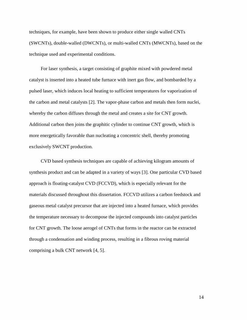
An individual CNT is comprised of a hexagonal arrangement of sp2 bonded C atoms
formed in a cylindrical geometry (as depicted in Figure 1a). The configuration of the
terminating atoms is formed based on the chiral angle connecting two
crystallographically equivalent points of the hexagonal lattice, which consequently
influences the electronic character of the nanotube. The chiral angle can range from 0° to
30°, where 0° forms a zigzag geometry at the terminating edge, while a chiral angle of
30° represents an armchair configuration. The resultant electronic properties of the CNT
can be approximated via the zone-folding approximation, which applies a periodic
boundary condition to the band structure of graphene to simulate the circular structure of
a CNT. In graphene, a Dirac cone is formed in the electronic band structure at the 6
corner points of the 1st Brillouin zone, whereby there is a zero band gap at the center of
the cone [1]. Therefore, if the periodic slices intersect the center of the Dirac cones,
metallic behavior is observed, which occurs in the case of armchair terminated CNTs.
Specific zigzag configurations also result in the metallic behavior due to slices crossing
through the center of the corner points of the 1st Brillouin zone. However, chiral angles
that result in slices passing through the tapering portion of the Dirac cone will be
semiconducting with a band gap related to the location of the slice. Additionally, the
number of concentric walls forming the CNT (see Figure 1b) influences the electronic
transport. Metallic behavior has been shown computationally for double walled CNTs,
even if the concentric walls are comprised of semiconducting nanotubes. The number of
concentric walls present tends to be influenced by the methods employed to synthesize
the CNTs. Laser vaporization and chemical vapor deposition (CVD) based synthesis
14
techniques, for example, have been shown to produce either single walled CNTs
(SWCNTs), double-walled (DWCNTs), or multi-walled CNTs (MWCNTs), based on the
technique used and experimental conditions.
For laser synthesis, a target consisting of graphite mixed with powdered metal
catalyst is inserted into a heated tube furnace with inert gas flow, and bombarded by a
pulsed laser, which induces local heating to sufficient temperatures for vaporization of
the carbon and metal catalysts [2]. The vapor-phase carbon and metals then form nuclei,
whereby the carbon diffuses through the metal and creates a site for CNT growth.
Additional carbon then joins the graphitic cylinder to continue CNT growth, which is
more energetically favorable than nucleating a concentric shell, thereby promoting
exclusively SWCNT production.
CVD based synthesis techniques are capable of achieving kilogram amounts of
synthesis product and can be adapted in a variety of ways [3]. One particular CVD based
approach is floating-catalyst CVD (FCCVD), which is especially relevant for the
materials discussed throughout this dissertation. FCCVD utilizes a carbon feedstock and
gaseous metal catalyst precursor that are injected into a heated furnace, which provides
the temperature necessary to decompose the injected compounds into catalyst particles
for CNT growth. The loose aerogel of CNTs that forms in the reactor can be extracted
through a condensation and winding process, resulting in a fibrous roving material
comprising a bulk CNT network [4, 5].
15
Figure 1 Rendering of a (a) SWCNT, (b) MWCNT, (c) bundle of SWCNTs. Graphics courtesy of Andrew Merrill as
part of Dr. Landi’s research group.
1.2 Bulk Carbon Nanotube Conductors
Bulk carbon nanotube (CNT) conductors have been extensively studied in recent
decades due to their excellent flexibility, corrosion resistance, mechanical, and electrical
properties [6, 7]. A driving force for the development of bulk CNT conductors towards
electrical applications is the promise of exceeding the conductivity of metals, which is
theoretically possible for an individual CNT. Ballistic conduction has been reported both
theoretically and experimentally [8–11], which would correspond to conductivities > 108
S/m for a 1 nm diameter and 1 µm length. However, these transport properties heavily
depend on individual CNT characteristics such as chirality and number of walls, which
govern the density of states and electronic band structure [12]. Consequently, a number
of issues arise when translating the properties of individual CNTs to the bulk scale. For
example, individual CNTs, when in close proximity, tend to agglomerate into bundles of
various sizes due to the strong interaction between the delocalized orbitals [13, 14]. The
bundling that occurs between the CNTs can, in turn, alter the electronic structure of the
CNTs. For example, bundling can induce a bandgap in Armchair CNTs, which otherwise
would have a zero-bandgap [15]. In general, bundling has been suggested to induce

16
scattering between the CNTs [16]. Moreover, the formation of a network leads to
additional parameters which impact transport. The overall electrical conduction in CNT
networks can be thought of as a sum of the individual electrical contributions stemming
from transport along individual CNTs (intra-CNT transport), as well as the conduction
between CNTs (inter-CNT transport).
The intra-CNT transport is greatly influenced by the presence of surface defects or
impurities located along the nanotube, which can arise as byproducts of synthesis.
Individual CNTs have been experimentally measured to have resistance per lengths on
the order of the 6 kΩ/µm [17], which is the theoretical quantum resistance limit for
SWCNTs [18]. However, this resistance is not reliably achieved due to the random
distribution of defects present after synthesis [19]. In fact, the difficulty in producing
homogenous defect-free CNTs leads to a large inconsistency in reported mean-free-path
(MFP) and R/L values [18, 20, 21]. Defects and impurities can act as scattering sites,
which greatly impact the MFP of electrons in 1D conductors.
Inter-CNT transport is otherwise affected primarily by the electrical barrier at the
contact point between intersecting CNTs, e.g. the junction sites. Junction resistance has
been reported to be a major contributing factor to the overall resistance in pristine CNT
networks via C-AFM studies, where current maps of the network reveal the transport
characteristics [22–25]. The junction resistance between two CNTs varies depending on
the electronic type of each nanotube. The contact resistance between similar electronic
type CNTs has been found to be far less than between electronically type mismatched
CNTs, with metallic-metallic junctions having the lowest contact resistance [22, 24].
17
Contact resistance can arise due to thin tunneling barriers present at the contacts, or by
the presence of Schottky barriers.
Models of the CNT network conduction have been developed, which describe
multiple competing effects in the conduction of electrons [16, 26]. Namely, charge carrier
conduction has partial contributions from metallic transport (limited by phonon
backscattering), tunneling through thin barriers, and variable range hopping between
spatially localized electronic states, which arise in highly disordered systems. The term
“variable range” stems from the fact that the electronic transition is not limited to
immediate neighbor states, but rather to other energetically favorable states depending on
the length of localization (i.e. extent of the wavefunction). An implication of this
phenomenon is that, as the temperature of the material increases, electrons in trapped
states may adsorb enough phonon energy to transition states and participate in
conduction, increasing the conductivity of the network. In fact, traditional metals
decrease in conductivity when temperature is increased, due to increased phonon activity,
which acts as a scattering mechanism for already free electrons. Bulk CNT networks, on
the other hand, have been shown to have an order of magnitude lower variation in
resistance with increasing temperature than traditional metals [27], making CNTs an
attractive material for high-temperature applications. The conduction behavior in bulk
CNT networks, therefore, differs greatly from traditional metals. As such, while
traditional metals have the advantage of high conductivity at the bulk scale, bulk CNT
networks exhibit favorable temperature dependent electrical properties. However, bulk
CNT networks still require advancement to realize their inherent conductive capabilities
for electrical applications.

18
Over the past decade, there has been a lot of attention focused on improving the
electrical conductivity of bulk CNT conductors. Post-processing techniques, for example,
have been explored to enhance the conductivity of bulk CNT networks via improving
alignment, bridging junctions, and/or modifying local electronic structure through
stretching [28], chemical doping [29–32], radial, solvent, or planar densifications [7, 33,
34], and thermal treatment [35]. Additionally, a hybridized metal-CNT network has been
of high interest in recent years as a means to achieve conductivities close to that of
metallic wires by bridging the resistive CNT junctions with highly conductive metals [27,
36, 37], while maintaining the favorable temperature coefficient of resistance (TCR) for
the CNT bulk materials [27, 37]. Utilizing metals for adhesion as opposed to non-metallic
adhesion materials is benefitted by the delivery techniques that can be adapted, such as
Joule-heating driven CVD, which can encourage site-selectivity of deposition to the
regions of the network that are benefitted the most [27], as will be discussed in more
detail later.
1.3 Metal-CNT Conductors
Hybridizing CNTs with metals is an attractive method toward improving network
conductivity, as the metals may serve to lower the electrical barrier between CNTs, as
well as fill out the void space with a conductive material. From the other perspective,
individual CNTs residing in a metal matrix can be thought of as ballistic transport centers
within the metal, improving the local transport throughout metal matrices, as described
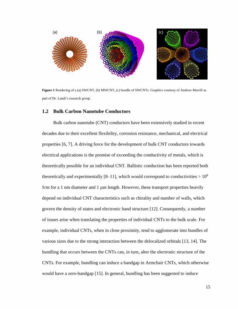
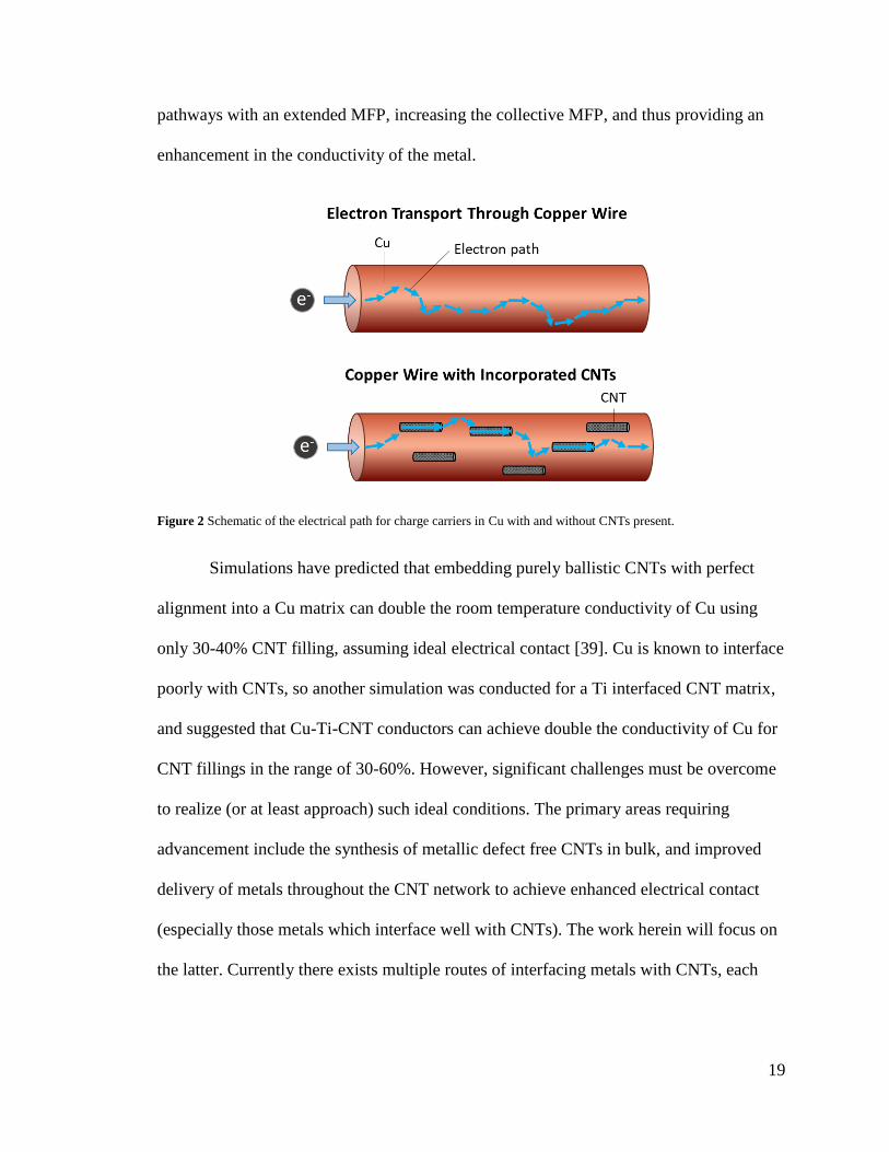
by Tokutomi et al. [38]. Charge carriers in a metal wire will scatter according to the
length of the MFP (see Figure 2). The presence of CNTs can act as local ballistic
19
pathways with an extended MFP, increasing the collective MFP, and thus providing an
enhancement in the conductivity of the metal.
Figure 2 Schematic of the electrical path for charge carriers in Cu with and without CNTs present.
Simulations have predicted that embedding purely ballistic CNTs with perfect
alignment into a Cu matrix can double the room temperature conductivity of Cu using
only 30-40% CNT filling, assuming ideal electrical contact [39]. Cu is known to interface
poorly with CNTs, so another simulation was conducted for a Ti interfaced CNT matrix,
and suggested that Cu-Ti-CNT conductors can achieve double the conductivity of Cu for
CNT fillings in the range of 30-60%. However, significant challenges must be overcome
to realize (or at least approach) such ideal conditions. The primary areas requiring
advancement include the synthesis of metallic defect free CNTs in bulk, and improved
delivery of metals throughout the CNT network to achieve enhanced electrical contact
(especially those metals which interface well with CNTs). The work herein will focus on
the latter. Currently there exists multiple routes of interfacing metals with CNTs, each
20
with their own advantages and disadvantages. The three primary routes that will be
explored here are PVD, CVD, and Electroplating.
1.3.1 Physical Vapor Deposition
The use of physical vapor deposition (PVD) can be employed for metalizing CNT
networks through methods such as thermal or e-beam evaporation [40–43] and
magnetron sputtering [44–48]. Thermal evaporation relies on ejecting atoms from a
source material via thermal stimulus and allowing them to condense onto a substrate. The
technique is carried out under vacuum, and thus the long mean-free-path for the vapor
particles enables uniform deposition along a topologically flat/smooth surface. However,
due to the line-of-sight nature of the technique, surface irregularities can cause
shadowing to occur, which results in non-uniform deposition. For a porous network (such
as that obtained by CNTs), these techniques offer limited penetrability, and provide
primarily surface coatings, as the top layer of CNT bundles will effectively mask or
shadow the underlying portions of the network. These techniques benefit from providing
very pure depositions, and are ideal for constructing layered conductors, or for probing
the interfacial interaction between the metals and the CNTs. These advantages make
PVD an ideal route for evaluating the surface interaction between metals and CNTs.
It has been hypothesized that the high energy of bombardment upon the CNT
substrate induced by incident sputtered metal atoms may lead to defects [49, 50], which
are claimed to localize electrons [49]. Electron localization results in an increase in the
network resistivity and is attributed to an increased sp2-sp3 rehybridization [51]. Janas,
et.al, found that, for Pt, Pd, Ag, and Au, sputtering indeed results in an increase in
resistance of the metal-CNT hybrid during the initial deposition stages [49]. Sputtering

21
Au onto a 10 µm thick CNT network had the greatest impact electrically (among the
metals studied), with a maximum increase in resistance of 200% compared to the starting
CNT network. In fact, for thinner CNT substrates (~100 nm), the impact on increased
resistance exacerbated, exhibiting a maximum increase in resistance of 1600% for the
Au-CNT network, further emphasizing the surface locality of the effect. However, after a
certain threshold of deposition time, percolation pathways formed which lead to a
reduction in electrical resistivity. With enough deposition time, the resistivity of the
networks eventually decreased beyond their starting resistance for all metals deposited.
Thus, PVD techniques can be used to fabricate metal-CNT conductors with improved
electrical properties, but may also impact the structure of the underlying CNTs.
1.3.2 Chemical Vapor Deposition
CVD is a popular technique for depositing metals onto topologically non-uniform
substrates due to its reactive nature, which allows for better conformality across irregular
and high-aspect ratio features [52]. Methods such as ALD are capable of achieving highly
controlled conformal coatings on CNT networks, however, can require several hundred
cycles (~1 min/cycle) to obtain thicknesses of ~15-30 nm for various metals [53, 54].
CVD otherwise offers a fast, scalable approach toward metal deposition, while still
enabling infiltration throughout CNT networks. Typically, a powder or liquid precursor is
brought into a vapor phase through applied heat. To reduce the precursor to a pure metal,
excess energy in the form of heat must be supplied to crack the ligand and decompose the
precursor. This excess heat can be applied after the vapor-phase precursor condenses onto
a cool substrate; otherwise the reduction can occur upon contact with an already hot
substrate (whereby the temperature exceeds the decomposition temperature).
22
There are multiple ways to provide heat to a substrate for decomposing the vapor-
phase precursor. An intriguing method in the context of CNT networks is Joule-heating
(or resistive heating). In this case, the resistive components of the network generate the
required energy for decomposing the precursors. At low currents, this lends the heating to
be site-specific in nature, spatially localizing the heat adjacent to the resistive regions in
the network. Alternatively, at sufficiently high currents, the lowest temperature anywhere
along the length of the conductor is above the decomposition temperature of the
precursor, in which case the deposition will tend toward a uniform distribution. Joule-
heating driven CVD is a novel delivery technique that has been established relatively
recently as an effective route for depositing metals into CNT networks for device
applications, whereby the metals preferentially deposit at the junctions sites between
contacting CNTs [55]. More recently, Leggiero, et al, have expanded this technique to
produce the first ever Joule-heating driven CVD-based bulk metal-CNT hybrid, whereby
site-specific depositions of Cu(tBaoac)2 were demonstrated, and full integration
throughout the thickness of the conductor was achieved [27]. This technique, when
combined with electroplating to interconnect the Cu seeds, led to a record conductivity of
28.1 MS/m for a conductor consisting of a mass percentage of 94.2% Cu w/w. Recent
advances in this technique render it a promising method toward high-conductivity bulk
CNT conductors.
1.3.3 Electrodeposition
A viable and well-studied route for delivering metals onto CNTs is electroplating
[27, 37, 50, 56–60]. Electroplating relies on the transfer of metal ions from a counter
electrode to a CNT working electrode through an electrolytic solution. Ions in solution

23
are adsorbed at the CNT surface via electrostatic attraction, and subsequently reduced by
the charged CNT interface or impurities [57]. As a result, electroplating can achieve
internal depositions within the CNT network via diffusion of ions in solution through the
network. The degree of internal plating depends on the rate of ion diffusion through the
CNT network relative to the deposition rate. Thus, surface plating can be encouraged by
increasing the current to the extent that deposition occurs more rapidly than ionic
diffusion through the CNT network [37]. As such, electroplating offers the tunability of
internal vs. surface depositions.
Hannula, et al, found that surface functionalization plays an important role in the
deposition properties for Cu electroplated CNTs [57]. It was found that Cu deposits in an
inhomogeneous manner on a pristine film comprised of >80% MWCNTs because of the
lack of active nucleation sites. On the other hand, oxygen functionalized films, produced
by thermal treatment in air or anodization, provided a highly active surface resulting in
uniform coatings. Surface activation via functionalization, however, increases the defect
content in the CNT film, evidenced by an increased D/G ratio. Increasing the
functionalization improves the hydrophilicity of the CNT film and provides more active
sites, however, excessive functionalization can severely impact the electrical properties of
the film. In such a scenario, there exists a trade-off between increased resistance and
improved wettability.
An alternative way to increase the amount of active sites is to perform a two-step
process, whereby the CNT conductor is first “seeded”, and then electroplated [27, 37,
50]. Such a method has been employed recently by Tran, et al, in which a wet-spun CNT
wire purchased through DexMat was sputtered with an Au adhesion layer, prior to Cu
24
electrodeposition [50]. Notably, electroplating the as-received CNT wire resulted in a
non-continuous Cu coating, with few nucleation sites leading to island growth in the
initial deposition stages. The Au sputtered CNT wire, however, had greatly improved
surface coverage during the initial deposition stages, with smaller and more abundant
nuclei. A previous study has shown that the presence of Au improves the hydrophilicity
of CNTs, which is important for the wetting of the aqueous electrolyte [49]. Additionally,
the Au provides uniform activation sites for nucleation during electroplating.
Furthermore, the Cu-Au-CNT wire achieved conductivities up to 80% of pure copper’s
conductivity and density savings up to 42%. Thus, metal seeding can offer an advantage
over oxygen functionalization for improving the electroplating deposition dynamics.
1.4 Metrics and Techniques
To quantify the performance of metals deposited onto CNTs via the
aforementioned methods, a variety of metrics are employed. Characterization of the
defect and elemental purity, conductivity, temperature dependent electrical properties,
and morphology, among other characteristics, provide crucial information toward
understanding the metal-CNT characteristics. Evaluating these properties is necessary to
quantify the advantages of the different deposition techniques and the improvements they
offer to the starting materials.
1.4.1 Conductivity, Specific Conductivity, and Temperature Dependent Resistivity
Volumetric and Specific Conductivity
Volumetric conductivity (or simply, conductivity) is a paramount metric for
assessing the performance of bulk CNT networks, and for drawing comparisons to
traditional metallic conductors. Bulk conductivity of a material is defined by three
25
parameters: the cross-sectional area of the conductor, A; and the resistance, R, over a unit
length, L. The equation governing conductivity is expressed as:
𝜎 =𝐿
𝑅⋅𝐴 (1)
Linear four-point probe measurements offer a reliable, facile method toward the
measurement of a material’s R/L, while circumventing the contact resistance of the
measurement probes. In this configuration, two outer probes supply current through the
conductor, while two inner probes separated by a distance, L, act as a voltage meter. The
R/L measurement can then be correlated with cross-sectional area to calculate
conductivity. The cross-sectional area can be either calculated based on optical
microscopy diameter measurements (for uniform cylindrical conductors) or obtained by
SEM (for irregular conductors).
A challenge that can arise when characterizing bulk CNT networks is the non-
uniformity in cross-sectional area that may be present along the length of the conductor.
In such cases, mass specific conductivity is a preferred metric, which evaluates the
electrical performance with respect to mass instead of cross-sectional area. Such a metric
can also be useful to determine weight-savings provided by the advanced conductors. The
mass specific conductivity is defined as follows:
𝜎𝑠𝑝 =𝜎
𝐷=
𝐿/𝑅𝐴
𝑀/𝐿𝐴=
𝐿2
𝑅𝑀 (2)
where D is the density of the conductor, and M is the mass of the conductor.
Measurement of the mass can be reliably made using a microbalance to provide the
necessary data for calculation of the specific conductivity.

26
Temperature Dependent Resistivity
Temperature dependent electrical behavior lends insight toward the interaction
between metals and CNTs. A vital component to hybridizing the CNTs with metals for
conductive applications relies on improving the conductivity of the CNTs while
preserving the beneficial temperature coefficient of resistance (TCR) properties inherent
to CNT materials. Several physical phenomena are responsible for the change in
resistance that materials experience under differing temperature conditions. In the case of
metals, phonons increase the amount of collisions that free electrons endure in their
conduction path, decreasing the MFP and increasing resistance at elevated temperatures.
However, for semiconductors, the extra energy can assist in breaking captive electrons
free from their host, allowing them to contribute to conduction at elevated temperatures.
In general, the temperature coefficient of resistance for metals, 𝛼0, is expressed as
𝛼0 =𝜌−𝜌0
𝜌0(𝑇−𝑇0) (3)
where 𝜌0 is the initial resistivity corresponding to an initial temperature, 𝑇0, and 𝜌 is the
final resistivity corresponding to an elevated or reduced temperature, 𝑇.
An additional factor governing the temperature dependent electrical properties of
metals is the metal grain structure. In fact, the measured TCR for electrochemically
deposited Cu interconnects has been demonstrated to vary with grain structure [61]. The
resistivity, 𝜌0, of a metal consists of two components: the temperature-dependent
component, which is influenced by phonon scattering, 𝜌𝑇(𝑇); and the scattering at
defects, surfaces, and grain boundaries, 𝜌𝑅, which is temperature-independent. Thus, the
27
resistivity can be expressed as 𝜌 = 𝜌𝑇(𝑇) + 𝜌𝑅 [61]. Therefore, to understand the role
that grain boundaries impart in the electrical behavior, the TCR can be rewritten as:
𝛼0 =𝜌𝑇(𝑇)−𝜌𝑇(𝑇0)
(𝜌𝑇(𝑇0)+𝜌𝑅)(𝑇−𝑇0) (4)
Consequently, it is evident that 𝛼0 will decrease with an increased 𝜌𝑅, which can arise
from a reduced grain size (or increased impurity concentration/crystal defects). While
grain expansion can be induced in thin copper films via annealing, the maximum size is
ultimately restricted based on film dimensions. A consequence of this is that, while the
thickness of a surface Cu film may be tuned by deposition parameters, depositions
internal to porous structures will ultimately be constricted in dimensions in accordance to
the pore confinements.
CNTs exhibit a more complex conduction behavior. Previous efforts have been
made to model the temperature dependent conduction behavior of CNT networks by
considering the different contributing factors to network conduction [16, 26], expressed
as:
𝜎(𝑇) = [𝐴exp (−𝑇𝑚
𝑇) + 𝐵exp (
𝑇𝑏
𝑇𝑠+𝑇)]
−1
+ 𝐻exp (−(𝑇0
𝑇)𝛾
) (5)
where A and B are coefficients related to morphology of the network (alignment, density,
etc.). The three terms correspond to the contributions from metallic conduction,
fluctuation assisted tunneling through thin barriers, and variable range hopping,
respectively. Energies of the respective components can be obtained by multiplying the
parameters by Boltzmann’s constant, kb. The energy kbTm is the metallic component that
28
corresponds to the backscattering energy of zone-boundary phonons for quasi 1-D
conductors. Charge carriers that exhibit metallic character in this way have improved
conduction at lower temperatures due to the lesser phonon activity. kbTb represents the
typical tunneling barrier energy which occurs between contact regions (CNT junctions),
and Ts/Tb relates to magnitude of the quantum resistivity in the low-temperature limit. T0
is a function of the electronic wave function localization length, which governs the
carrier’s ability to tunnel between localized states with assistance from phonon
absorption (VRH). As such, the relative sensitivity of this term to change in temperature
strongly depends on the localization length. Additionally, the dominance of this term is
influenced by the degree of localized states within the network. For thicker networks, a
greater number of metallic percolation pathways become available, and the VRH term
becomes negligible. For thinner networks, however, localized states represent a greater
proportion of the network, and the VRH term becomes an important consideration. The
location of localization is represented by 𝛾 =1
1+𝑑, where d is the dimensionality. In this
case, a dimensionality of 1 suggests intra-CNT localization, whereas d = 2 or 3 suggests
inter-CNT localization. These models have had success in fitting to measured data for
CNT networks and lends insight toward the character of different networks.
Temperature dependent conductivity measurements can be made at RIT are using
a commercial JANIS cryostat (see Figure 3) which handles temperatures ranging between
77 K – 800 K under vacuum (low 10-6 mbar). The temperature controller and four-point
probe equipment are interfaced with LabVIEW for precise temperature control and
electrical measurements. Measurements are typically made by recording IV sweeps at 5
degree increments at temperatures ranging from 300 – 600 K.

29
Figure 3 Left image: Vacuum pump (left), temperature controller (center), and JANIS cryostat (right). Right image:
JANIS cryostat four-point probe stage.
To gain insight toward the interaction between CNTs and deposited metals, a parallel
resistor model was developed [27] which treats the systems as two independent layers (no
interaction between CNTs and Cu), and can be expressed as
1
𝑅(𝑇)𝑡𝑜𝑡=
1
𝑅(𝑇)𝐶𝑢+
1
𝑅(𝑇)𝐶𝑁𝑇 (6)
where R(T) is the resistance as a function of temperature. In this case, resistance is
obtained via each materials’ measured specific conductivity, and R(T) is subsequently
calculated by using each materials’ corresponding TCR values. A sample which adheres
to the model reflects a non-interacting bilayer system. Deviation from this model
otherwise suggests that interaction between the materials exists. Thus, various models
can be applied to understand the conduction behavior of the metal-CNT networks as well
as whether interaction exists between the hybrid components.
1.4.2 Morphology Analysis (SEM)
Scanning electron microscopy (SEM) is a powerful tool for qualitatively
identifying the presence of particles (such as catalysts) in the network, as well as

30
assessing the microscopic morphology of the network and particles within it.
Additionally, SEM can be used to directly measure the cross-sectional area of the CNT
conductors. Due to the irregular nature of bulk CNT networks, cross-sectional
measurements may require specialized techniques to prepare the samples for SEM
imaging. Several methods exist to achieve cross-section preparation, each with their own
advantages and disadvantages. RIT has the capability to perform cross-sectioning via
epoxy-setting followed by microtoming, laser-cutting using a Forest Scientific 30 W
VLS2.30 CO2 laser, or razor slicing. The first option, microtoming, offers minimal
distortion to the cross-sectional area size, but is time and labor intensive. Laser-cutting
provides a rapid method of cutting CNT wires for cross-sectional assessment, however,
the local heat generated may lead to metal migration and/or flaring of the CNT bundles in
the network, distorting the cross-sectional area. Razor slicing also offers the advantage of
speed, however, may disturb the morphology of the cross-section area by pulling out
CNTs, and distorts the area through compression. As such, each of these techniques
presents their own challenges. Therefore, careful consideration must be made when
selecting the technique, depending on the application and desired analysis.
1.4.3 Elemental Characterization (XRD, Raman, EDX)
Scanning electron microscopes are capable of performing X-ray microanalysis to
determine the elemental profile present within a specimen. The technique is performed by
bombarding the sample with electrons whose energies are on the order of the binding
energy of the element’s core electrons. The excited core electrons then relax, emitting
photons in the X-ray range. The amount of orbital shells and occupancy of the subshells
within the host atom dictate the amount of energy required to excite the electron. Thus,
31
each element can be uniquely identified by collecting the characteristic X-ray emission
using a detector that is equipped on the SEM. This technique, referred to as energy
dispersive spectroscopy (EDS), is useful for analyzing the carbon and metal distribution
in the CNT hybrids.
Another X-ray related technique that can be used to identify the presence of
specific elements is X-ray diffraction (XRD). In compliance with the Bragg condition, an
X-ray beam of a particular energy is directed at a crystalline sample and undergoes
constructive interference at allowed diffraction angles dependent on the lattice spacing.
The sensitivity of this technique to the lattice parameters provides characteristic
measurements for elements as well as compounds such as oxides. Thus, XRD can help
determine whether the deposition of metals onto CNTs results in a metallic film, or forms
carbides/oxides.
A third spectroscopy technique, which is powerful for probing low-frequency
modes (e.g. vibrational and rotational), is Raman spectroscopy. In this case, incident
radiation in the visible, near-UV, or near-IR region is inelastically scattered (i.e. the
photons exhibit a different energy upon scattering) with an energy shift related to the
molecule’s nuclear vibrations. Molecules may exhibit multiple types of vibrational states
which may be unique to the molecule, enabling the identification of compositional
information as well as crystallinity of a structure. In the context of CNTs, the relative
defect ratio can be revealed through the presence of the D peak, as phonons responsible
for this signal are forbidden in sp2-bonded carbon. Additionally, the presence of certain
carbides and oxides can be identified by their vibrational modes, enabling this technique
to determine the state of certain metal films deposited onto the CNTs, lending insight
32
toward the bonding characteristic of the metals with the CNTs. In general, the variety of
characterization techniques described above are paramount for understanding the
metal:CNT interaction, and helps to identify the compatibility of the different metals with
CNTs.
1.5 Interaction of Metals and CNTs
1.5.1 CNT-Metal Compatibilities
An issue that arises with the integration of certain metals, such as Cu, is their poor
adhesion when deposited onto CNTs [45, 62], which prevents full utilization of the
potential electrical benefits provided by the hybrid conductors. A qualitative indication of
the wettability of metals on CNTs is the morphology that they take upon deposition,
which can be observed using SEM or TEM. The morphology of a fairly thorough survey
of metals as deposited onto individual CNTs has been performed by Zhang, et al, in 2000
[63, 64]. Specifically, Ti, Ni, Pd, Au, Al, and Fe were deposited at 5 nm and 15 nm
thicknesses using e-beam evaporation. Ti is shown to exhibit the best wettability amongst
the metals studied, as it deposits uniformly and continuously along the CNTs. Ni and Pd
are also shown to deposit mostly continuously, in the form of discrete particles, with
some degree of interruptions along the length of the coating. Au, Al, and Fe, on the other
hand form discrete islands as deposited. In fact, the size of the deposited Au clusters have
a bigger diameter than the thickness of the deposited coating, indicating migration of the
Au to minimize surface energy.
The deposition dynamics are largely dependent on the interaction between the
substrate and the condensate. The diffusion rate of adatoms on a surface is proportional to
the energy required for diffusion (𝐸𝑑𝑖𝑓𝑓) by exp(−𝐸𝑑𝑖𝑓𝑓/𝑘𝐵𝑇), where 𝑘𝐵 is the
33
Boltzmann constant, and T is temperature [65]. Thus, a lower diffusion energy results in
a higher rate of diffusion. The diffusion energy has been empirically determined to be
proportional to the binding energy, 𝐸𝐵, as 𝐸𝐷𝑖𝑓𝑓~𝐸𝐵/4 [65]. Accordingly, a strong
binding energy between the two constituents results in slow surface diffusion, which
results in a higher nucleation density. A weak binding energy, otherwise, permits fast
surface diffusion such that adatoms can find already formed nucleation centers and merge
to induce island growth. Thus, the morphology observed for the deposited metal atoms on
CNTs gives qualitative insight toward their binding energy and interaction.
Attempts to explain the interaction between CNTs and metals has proven
challenging, and groups have focused on correlating a variety of different parameters to
explain the behavior observed. For example, Zhang, et al, explained the results observed
in their evaporation studies described earlier [63, 64] based on the reactivity of bulk
carbon with the respective metals. Metals can interact with carbon in a variety of ways.
Fe, for example, is capable of dissolving carbon well for catalytic applications, while Ti
limits the mobility of the carbon as it locks the carbon into a carbide [66]. Metals like Cu
are otherwise inert to carbon. The range of interactions is explained by the bonding
behavior between carbon and the respective transition metals, for which, the carbon p-
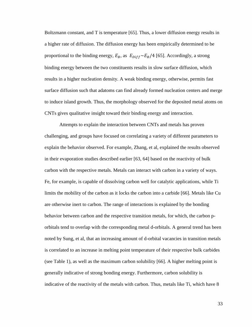
orbitals tend to overlap with the corresponding metal d-orbitals. A general trend has been
noted by Sung, et al, that an increasing amount of d-orbital vacancies in transition metals
is correlated to an increase in melting point temperature of their respective bulk carbides
(see Table 1), as well as the maximum carbon solubility [66]. A higher melting point is
generally indicative of strong bonding energy. Furthermore, carbon solubility is
indicative of the reactivity of the metals with carbon. Thus, metals like Ti, which have 8
34
d-orbital vacancies, react very readily with carbon to form carbides, and as such have
limited solubility. Metals like Fe and Ni, on the other hand, are capable of dissolving a
substantial amount of carbon without fully locking up in carbides, due to their moderate
reactivity [66]. Lastly, metals like Cu have very limited interaction with carbon and
exhibit no carbon solubility as a result.
Table 1: A list of metals and their corresponding number of d-orbital vacancies, as well as the melting point for the
respective stable carbide types. Lastly, effective eutectic solubilities at 1000 °C for C in molten transition metals. All
data obtained from Sung, et al [66].
The reactivity of metals with carbon is an important factor regarding the expected
bonding and adhesion characteristics. However, the electrical interaction between metals
and CNTs is another critical factor when considering their use for fabricating hybrid
conductors. A primary consideration is the contact resistance between the metals and the
CNTs, which can arise from the tunneling barriers generated by work function mismatch
[67, 68] as well as the contact geometry [69]. Furthermore, the electrical contact can be
influenced by adsorbates present on the CNTs, which modify the local density of states
35
(DOS) [70–72]. Adsorbates can arise from atmospheric or environmental exposure,
whereby the CNT’s non-localized π-electrons enable the sidewalls to form weak van der
Waals bonds with ambient molecules. Such adsorbates have been reported to measurably
influence the electrical conductivity of CNTs [73, 74], and in some cases decrease the
contact resistance [75].
More generally, however, wetting geometry imparts a significant role in contact
resistance between metals and CNTs. It is reported that, with poor wetting, the contact
area between the metal and the CNT decreases, and the work function difference
dominates the resistance [67]. Thus, these two factors must be considered when assessing
metal-CNT compatibility for electrical interfacing. Lim, et al., created a plot of metal-
CNT contact resistances versus the work function of the metals [67]. While Ti deviates
from the typical range of CNT work functions, it exhibited the lowest contact resistance
as a result of its excellent wetting to CNTs. Metals like Cu, on the other hand, exhibited
moderate contact resistance, despite having a matched work function, due to its poor
wettability.
As mentioned previously, good wettability has been associated with a high
amount of d-orbital vacancies. This trend has been observed for contact resistance as
well, in a study performed by Liebau, et al [76]. In this study, individual CNTs were
contacted by either Au/Fe, Pd, or Co electrodes to measure contact resistance via a two-
point probe method, which measures the intrinsic CNT resistances as well as the contact
resistances. A four-point probe method was used to measure the intrinsic resistance of 5
individual CNTs, which would serve as the CNT contribution to the resistance obtained
via the two-point probe measurements. In the case of the Au/Fe electrode, the CNTs
36
exhibited the highest resistances measured (20 MΩ – 2.5 GΩ). Pd exhibited much lower
resistances, between 70 – 450 kΩ. Co contacted CNTs, having the most d-orbital
vacancies, resulted in resistances below 150 kΩ. This demonstrates a trend that higher
metal d-orbital vacancy leads to improved contact resistance with CNTs, both of which
have previously been correlated with good wettability.
Metals with the highest conductivities often have few to no d-orbital vacancies
(such as Ag and Cu), and thus, interact poorly with CNTs. Therefore, when preparing
bulk metal-CNT hybrid conductors, an interfacial layer is necessary to improve the
contacting and interaction between the CNTs and the respective conductive metal
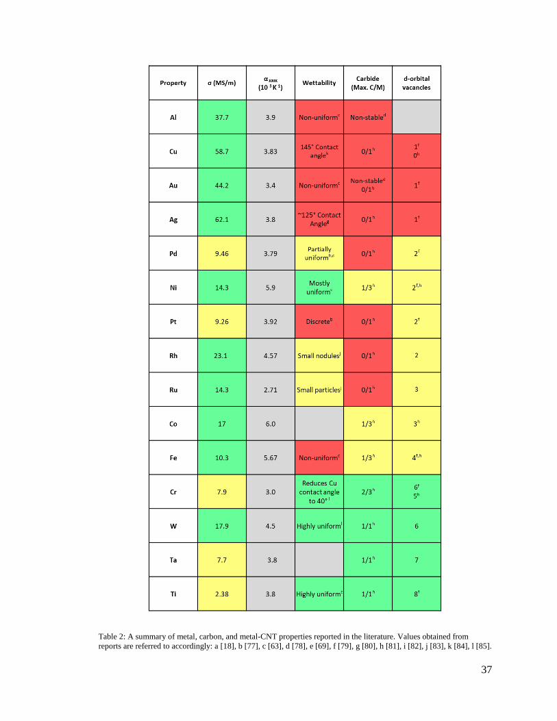
coating. Table 2 shows a summary of all the important considerations to bear for metal-
CNT conductor design, with metals ordered by their number of d-orbital vacancies. A
green cell indicates properties that are well aligned with intermixing of metals and
carbon, and suitable for high performance. Yellow cells indicate limited interaction or
performance, while red indicate very poor interaction or performance. Information for
some metal:CNT interaction properties are not readily available and are shaded grey.
Based on the collection of reported values, metals such as Al, Cu, Au, and Ag, while
highly conductive, will require an interfacing component if to be used with CNTs. Ti and
Ni are two candidates that stand out as promising adhesion metals, with overall good
compatibility with CNTs. As such, Ni and Ti have been selected for evaluation herein.
37
Table 2: A summary of metal, carbon, and metal-CNT properties reported in the literature. Values obtained from
reports are referred to accordingly: a [18], b [77], c [63], d [78], e [69], f [79], g [80], h [81], i [82], j [83], k [84], l [85].
38
1.5.2 Ni Compatibility for CNT Hybrids
Previous studies have shown that Ti and Ni have favorable wettability on CNTs, as well
as good electrical contact [63, 86], whereas metals such as gold, aluminum, and iron
show poor wetting properties[63]. In the case of Ni, Menon et al. found computationally
that the curvature of the CNTs can promote rehybridization of the carbon sp2 orbital with
the Ni d-orbital, altering the bonding characteristics from that experienced between Ni
and bulk carbon [87]. This motivates the use of Ni for use in bulk metal-CNT hybrid
conductors.
Zou et al. used electrodeposition to fabricate a bulk Cu-Ni-CNT conductor
consisting of a nanoscale Ni layer and a 2 µm thick Cu layer. Samples were annealed in
Ar for 30 minutes at 300 °C, resulting in a conductivity greater than 20 MS/m, and a
temperature coefficient of resistance as low as 1.14 × 10⁻³ K-1 [62]. Zou et al. showed via
cross-sectional electron microscopy that an annealed Cu-CNT conductor fabricated
without a Ni adhesion layer resulted in microgaps at the Cu-CNT interface, due to poor
wettability of the Cu. With the use of a Ni buffer layer, however, a well-connected
interface was formed, demonstrating the ability of Ni to interface well with CNTs.
However, another important aspect to note is that the Ni diffuses through the Cu layer
due to the mutual compatibility of the metals, as evidenced by an EDX line scan.
The impact that annealing has on the diffusion of Ni within the Cu layer was
further illustrated using surface EDX mapping, whereby the Ni signal became more
homogeneous after annealing. This can have a variety of consequences on the electrical
properties of Cu. For example, a previous study has shown that the conductivity of
electrodeposited Ni-Cu alloys decreases with increasing Ni content [88]. In this case,
39
diffusion of Ni into Cu should be limited. On the other hand, constantan is a Ni/Cu
(~45%/55%) alloy, which is known for its extremely low TCR of ~5.0 × 10⁻⁶ K-1 [89].
Thus, the observed low TCR for this Cu-Ni-CNT hybrid may be partially benefited by
the diffusion of the Ni into the Cu layer, although the true origin of this low TCR is not
fully understood. In this paper, it is speculated that partial elastic scattering at the surface
could possibly be reducing the TCR, however no evidence is provided. Regardless, Ni is
shown to interface well with CNTs as well as Cu, showing promise from a wettability
standpoint.
Milowska et al. have studied the interaction between Cu, Ni, and Cr with CNTs as
deposited (via magnetron sputtering) and after exposure to elevated temperatures
(ranging from 400 to 1000 °C) [45]. Electron microscopy images indicate that melting of
the Cu is observed at temperatures as low as 400 °C, leading to severe de-wetting at 600
°C, and eventually evaporation at 1000 °C. In the Cu-Ni-CNT system, however,
significant beading was not observed until 800 °C, with Ni remaining at 1000 °C after the
Cu evaporates. Furthermore, some amount of metal was visible beneath the CNT surface
in the Cu-Ni-CNT, suggesting a much greater interaction between the metals and the
CNTs. However, the high degree of interfacial interaction provided by the Ni comes at
the cost of degradation of the CNT structure. Milowska et al. measured higher D/G ratios
for the Cu-Ni-CNT system as the annealing temperature increased, attributed to the
solubility of carbon in Ni (which is corroborated by EDX measurements). The solubility
of carbon within the Ni is decreased with the presence of Cu, and thus, while Ni provides
great surface interaction with CNTs, careful considerations must be made regarding
applied temperatures and metal combination selection.
40
1.5.3 Ti-CNT Interaction
Ti is among the most reactive metals with CNTs, indicating superior wettability
[63] and binding [66], as well as electrical contact [67]. Computational studies
performed by Yang et al. investigated the adsorption of continuous Ti, Au, and Al chains
(linear connection of metal atoms) on various SWCNT surfaces and found that Ti is
energetically more favorable [90]. Their ab initio calculations determined binding
energies of 0.25 eV/metal atom and 0.52 eV/atom for Au and Al, respectively, while Ti
had binding energies as high as 2.04 eV. Moreover, it was found that the Ti chain imparts
a DOS at the Fermi level for the Ti deposited SWCNT, giving rise to metallic behavior
for an otherwise semiconducting SWCNT. First principle calculations were also carried
out on the bonding distance and electrical contact properties of metals on graphene and
SWCNTs by Matsuda et al. [91]. Ti was shown to exhibit the smallest bonding distance
on graphene at 2.17 Å, and a high binding energy of 2.09 eV. Further calculations were
conducted for (13,0) SWCNTs, resulting in an even smaller bonding distance of 2.11 A,
attributed to the curvature of the SWCNT. Matsuda’s calculations determined that the
interaction between the d-orbitals of the metals and carbon’s pπ orbitals have a critical
impact on the electrical and bonding characteristics imparted to the metal-CNT systems.
Electrical characteristics were probed by constructing I-V models to calculate the contact
resistances of the metals with the CNTs. Ti was found to have an extremely low contact
resistance on (7,7) SWCNTs of 6.9 kOhm/nm, an order of magnitude lower than the next
best contact resistance found (63.7 kOhm/nm for Pd-SWCNT). Overall, computational
studies have good agreement that Ti has highly favorable characteristics as deposited on
CNTs.
41
Zhang et al. also provided experimental evidence of the strong adhesion between
Ti and CNTs [63, 64]. As mentioned previously, Zhang coated individual CNTs with
various metals and found that Ti forms continuous coatings along the surface of the
CNTs [63]. In a follow up study, they coated CNTs with 1 nm of Ti and investigated the
coating properties of various other metals deposited onto the Ti-CNT system [64].
Electron microscopy images showcased that 5 nm coatings of Au, Pd, Fe, Al, and Pb onto
individual SWCNTs resulted in mostly discontinuous coatings as deposited. However, a
1 nm Ti adhesion layer was capable of significantly improving the wettability of all
metals studied, resulting in nearly continuous coatings for even the least compatible
metals.
Experimentally, the use of a Ti layer on CNTs has also been prevalent in
nanoelectronics, whereby Ti improves the contact resistance between CNTs and their
respective substrate [92, 93]. Srividya et al. found that as-grown vertically aligned CNTs
using an Fe catalyst exhibited poor adhesion with a Si substrate (with CNTs detaching
from the surface), whereas a Ti buffer layer provided sufficient support to maintain
adhesion of the CNTs [93]. Additionally, it has been reported that the high CNT-substrate
contact resistance can lead to excessive Joule-heating, eventually damaging/evaporating
the CNTs, resulting in a reduction in emission current for the CNT devices [94]. This
effect is witnessed in the CNT devices that Srividya et al. fabricated without the Ti
adhesion layer. However, the use of a Ti adhesion layer maintains a stable emission
current for extended periods of time, attributed to the lowering of the contact resistance
from the Ti-CNT interface (resulting in less Joule-heating).
42
Additionally, in a study performed by Chu et al., Ti was shown to exhibit strong
interfacial interaction in a Cu-Ti/CNT metal composite matrix while having no negative
impact on electrical conductivity with up to 15% CNTs by volume [95]. In this study,
Cu-Ti/CNT composites were prepared via mechanical ball milling of either Cu or
prealloyed Cu-Ti (0.85% Ti, 8-20 µm in size) powders and MWCNTs. The prepared
composites consisted of 0, 5, 10, and 15% wt CNTs and were tested for yield strength
and electrical conductivity. A measurably higher yield strength was evident for the Cu-
Ti/CNT composite and is attributed to a couple of factors. Namely, the presence of Ti
itself can slightly improve the resistance to plastic deformation by impeding the
movement of lattice dislocations. Moreover, Chu et al. observed the presence of TiC
(111) lattice fringes via HRTEM imaging, the presence of which may significantly
improve the interfacial interaction between the Cu and the CNTs and the corresponding
load-transfer ability. Furthermore, while the yield strength is improved significantly with
the presence of a Ti buffer, the electrical conductivity is unaffected. This suggests that Ti
is a very effective adhesion metal for use in Cu-CNT composites, which can improve the
interfacial interaction without negatively impacting the electrical performance.
2 Opportunities for Advancement & Dissertation Goals
2.1 Evaluation of Adhesion Metals for Metal-CNT Hybrid Conductors
Ti and Ni have shown promising adhesion properties as-deposited, however,
studies to date have focused on room temperature electrical variation and microscale
behavior, whereas understanding how adhesion metals on bulk networks are stable at
increased temperature due to operation conditions (such as motors) or under increasing
applied current [7, 27] is warranted. As highlighted earlier, Milowska et al. have studied
43
the effects of high-temperature annealing (400 °C to 1000 °C) on Cu-Ni-CNT
composites, finding that the Ni experiences a complex solubility with both Cu and CNTs
[45]. The effectiveness of Ti as an adhesion layer for conductive Cu-CNT hybrids at
elevated temperatures is yet to be reported. In fact, there has been very limited research in
general investigating the use of Ti as an adhesion layer for bulk metal-CNT hybrid
conductors. Much of the research to date on Ti-CNT structures are based in
microelectronics or MMC’s for mechanical purposes, which have demonstrated the clear
advantages that Ti shows as an electrical interface for CNTs. Utilizing Ti as an adhesion
layer for metal-CNT hybrids could offer the advantages of improving wettability of
conductive metal overcoats as well as provide an electrical interface capable of allowing
charge transfer due to its low contact resistance with CNTs.
2.2 Scalable Fabrication Methods Towards Ti-rich Integrated Conductors
One of the critical challenges with integrating Ti into bulk CNT networks is the high
reactivity of Ti and its corresponding tendency to form oxides. As a result of its high
reactivity, electrodeposition of metallic Ti is particularly challenging, often resulting in
depositions of various Ti compounds based on the media used [96–98]. Therefore, PVD
techniques offer an easy route for the deposition of pure Ti. However, due to the limited
penetrability of PVD techniques, they are not a viable solution for fabricating integrated
metal-CNT conductors. Joule-heating CVD based delivery offers a promising route
toward the fabrication of integrated Ti-CNT conductors, with the advantage of
maximizing metal-CNT interfacial area for enhanced interaction. There has been limited
work on the deposition of pure Ti onto bulk CNT networks through the Joule-heating
CVD method, as the technique is relatively recently developed for bulk CNT networks..
44
Such a technique would be suitable as a scalable fabrication method for fully integrated
Ti-CNT conductors, which can then be processed further to bridge the CNT bundles and
junctions with highly conductive metals that are typically incompatible with CNTs.
Ultimately, CVD deposited Ti-CNT conductors can enable the fabrication of high-
performance metal-CNT hybrids, mitigating the connectivity issues, improving their
temperature stability, and enhancing their electrical performance.
2.3 Dissertation Objectives
The aim of this dissertation is to optimize the fabrication of 3D Cu-Ti-CNT hybrids for
development of highly conductive, temperature-stable wires with favorable temperature
dependent electrical properties to provide energy savings in elevated temperature
applications. Developing an understanding of the relationship between metallization
processing conditions and resultant material characteristics is key for the fabrication of
high performance metal-CNT hybrids. The major focus areas in this dissertation are
subdivided below:
1. Evaluation of the electrical performance, temperature stability, and wettability of 2-D
Ti and Ni as adhesion metals for bulk Cu-CNT conductors via thermal evaporation.
2. Fabrication of high conductivity 3-D Cu-Ti-CNT hybrids combined with low TCR by
means of a Joule-heating CVD technique and electroplating.
3. Demonstration of Ti-rich depositions achieved via development in CVD processing
conditions. Assessment of the influence of CVD conditions on the nanoscale
interconnection characteristics by employing temperature-dependent electrical
modeling.

45
3 Evaluation of Ti and Ni as Adhesion Metals
3.1 Thermal Evaporation and Annealing
The use of physical vapor deposition (PVD) can be employed for metalizing CNT
networks through methods such as thermal or e-beam evaporation [40–43] and
magnetron sputtering [44–48]. In our recently published work, a thermal evaporation
technique was used to deposit thin metal films onto a CNT conductor, followed by
annealing, for assessing adhesion via scanning electron microscopy (SEM) analysis and
electrical characterization [99]. PVD was selected as a means to achieve a well-defined
thin-film interface for assessing the benefits of an adhesion layer towards scalable
designs. Samples were annealed at temperatures between 100 °C and 400 °C, a
temperature range which could be reached during the operation of motor applications or
during fabrication of the Cu-CNT conductors [27]. Furthermore, temperature-dependent
electrical measurements were conducted from 26.85 °C to 326.85 °C (300 K to 600 K) to
understand the permanent electrical effects that processing at elevated temperatures has
for the various hybrid conductors. Identification of a conductive adhesion metal for the
Cu-MA-CNT is critical for designing hybrid conductors, which can eventually replace
conventional conductors in applications in which they are exposed to elevated
temperatures. The following work in this section has been reprinted with permission from
(McIntyre, D. J., et al, Enhanced Copper–Carbon Nanotube Hybrid Conductors with
Objectives
— Assess the morphology of Ti and Ni deposited onto CNTs via thermal evaporation.
— Determine the stability of 10 nm Ti and Ni layers, and 100 nm Cu layer, on CNTs
after exposure to elevated temperature
— Study the electrical properties of Cu-MA-CNT hybrids and their temperature stability.
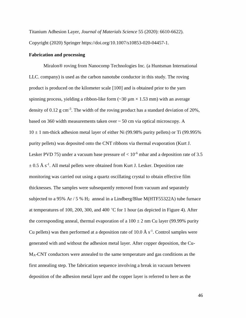
46
Titanium Adhesion Layer, Journal of Materials Science 55 (2020): 6610-6622).
Copyright (2020) Springer https://doi.org/10.1007/s10853-020-04457-1.
Fabrication and processing
Miralon® roving from Nanocomp Technologies Inc. (a Huntsman International
LLC. company) is used as the carbon nanotube conductor in this study. The roving
product is produced on the kilometer scale [100] and is obtained prior to the yarn
spinning process, yielding a ribbon-like form (~30 µm × 1.53 mm) with an average
density of 0.12 g cm-3. The width of the roving product has a standard deviation of 20%,
based on 360 width measurements taken over ~ 50 cm via optical microscopy. A
10 ± 1 nm-thick adhesion metal layer of either Ni (99.98% purity pellets) or Ti (99.995%
purity pellets) was deposited onto the CNT ribbons via thermal evaporation (Kurt J.
Lesker PVD 75) under a vacuum base pressure of < 10-6 mbar and a deposition rate of 3.5
± 0.5 Å s-1. All metal pellets were obtained from Kurt J. Lesker. Deposition rate
monitoring was carried out using a quartz oscillating crystal to obtain effective film
thicknesses. The samples were subsequently removed from vacuum and separately
subjected to a 95% Ar / 5 % H2 anneal in a Lindberg/Blue M(HTF55322A) tube furnace
at temperatures of 100, 200, 300, and 400 °C for 1 hour (as depicted in Figure 4). After
the corresponding anneal, thermal evaporation of a 100 ± 2 nm Cu layer (99.99% purity
Cu pellets) was then performed at a deposition rate of 10.0 Å s-1. Control samples were
generated with and without the adhesion metal layer. After copper deposition, the Cu-
MA-CNT conductors were annealed to the same temperature and gas conditions as the
first annealing step. The fabrication sequence involving a break in vacuum between
deposition of the adhesion metal layer and the copper layer is referred to here as the

47
“two-step” deposition process. An additional set of samples were fabricated by depositing
the adhesion metal layer and copper layer sequentially, without breaking vacuum,
referred to as the “one-step” deposition process.
Characterization
Analysis of film morphologies was performed using a Hitachi S-900 scanning
electron microscope (SEM) equipped with a secondary electron detector and biased at 2
kV accelerating voltage. Current-voltage sweeps (up to 100 mA) were conducted in an
ambient atmosphere at room temperature using a four-point-probe configuration with a
National Instruments NI PXI-5652 source/measure unit and NI PXI-4071 digital
multimeter. The probe tips were bent in a configuration that applies firm contact but
prevents penetration through the top layers of the samples (i.e. a dull contacting point
rather than a sharp contacting point). Temperature-dependent electrical measurements
were performed in a Janis cryostat under 10-6 mbar vacuum. Two cycles of temperature
sweeps over 26.85 – 326.85 °C (300 – 600 K) were performed with four-point probe I-V
sweeps being carried out at 5 °C increments. A National Instruments NI PXI-4110
programmable power supply and NI PXI-4072 digital multimeter were used to acquire
the electrical measurements.

48
Figure 4 (a.) SEM images of the starting CNT conductor material. (b.) Experimental process for studying
the CNT-metal interfacial interactions [99].
SEM Analysis
The SEM image in Figure 4a was acquired from the surface of the CNT conductor used
in this study, showing the network morphology of the CNT bundles. The presence of
residual iron catalyst and carbonaceous material from synthesis is visible. The porosity of
the network on the nanoscale enables infiltration of the metals and a greater surface area
for deposition. Meanwhile, the planar ribbon geometry of the material provides a
relatively flatter surface for line-of-site metal deposition than a wire-like format.
The processing steps used for the study of adhesion metals are summarized in
Figure 4b. Additionally, as a point of comparison for the Cu-MA-CNT conductors, a Cu-
CNT conductor was fabricated and subjected to the annealing steps. The SEM images in
Figure 5 show the morphology of a 100 nm Cu layer directly deposited onto the CNT
conductor followed by subsequent annealing treatments at 100, 200, 300, and 400 °C.
The morphology at each processing step was analyzed and compared against electrical
measurements to quantify the performance of the Cu-CNT system. The annealing
sequence performed on the Cu-CNT conductor provides a benchmark by which the

49
performance of the Cu-MA-CNT may be compared. Due to its thickness, the Cu layer
initially forms a continuous film along the CNT network as-deposited, with an average
grain size of 58 ± 6 nm measured based on SEM images. A gradual evolution of the Cu
grain structure is observed upon exposure to elevated temperatures. At an annealing
temperature of 100 °C, the onset of grain growth is observed with grain size increasing to
a measured 71 ± 1 nm. As the temperature is increased to 200 °C, more evident
coalescence is observed as the average grain size increases to approximately 137 ± 9 nm.
Grain growth appears to peak toward an average size of about 167 ± 7 nm at temperatures
of 300 °C. Similar grain growth effects have been observed on nanocrystalline Cu thin
films sputtered onto Cu substrates, whereby grain growth is observed at temperatures as
low as 100 °C and increases at temperatures of 300 °C [101]. However, the Cu grain size
appears to decrease for the 400 °C anneal, with an average size of 121 ± 7 nm. The
reduction in size is attributed to the Cu layer beginning to discretize, confining the area
for grain expansion. This is accompanied by delamination into an independent film,
consistent with a previous report in the literature, where melting of thin Cu films on
MWCNTs was observed at temperatures of 400 °C [45], and attributed to nanoscale
induced melting point depression [102]. Furthermore, poor wettability is evidenced by
the non-coated CNTs becoming visible between gaps generated during delamination in
the post-annealed Cu layer (as shown in Figure 5e). The observed delamination indicates
a need to introduce an adhesion metal to the Cu-CNT conductor to improve the stability
of the Cu overlayer when exposed to high temperatures. For applications in which the
conductors operate at elevated temperatures, the electrical performance of Cu-CNT wire
technologies must be stable upon exposure to these increased temperatures.
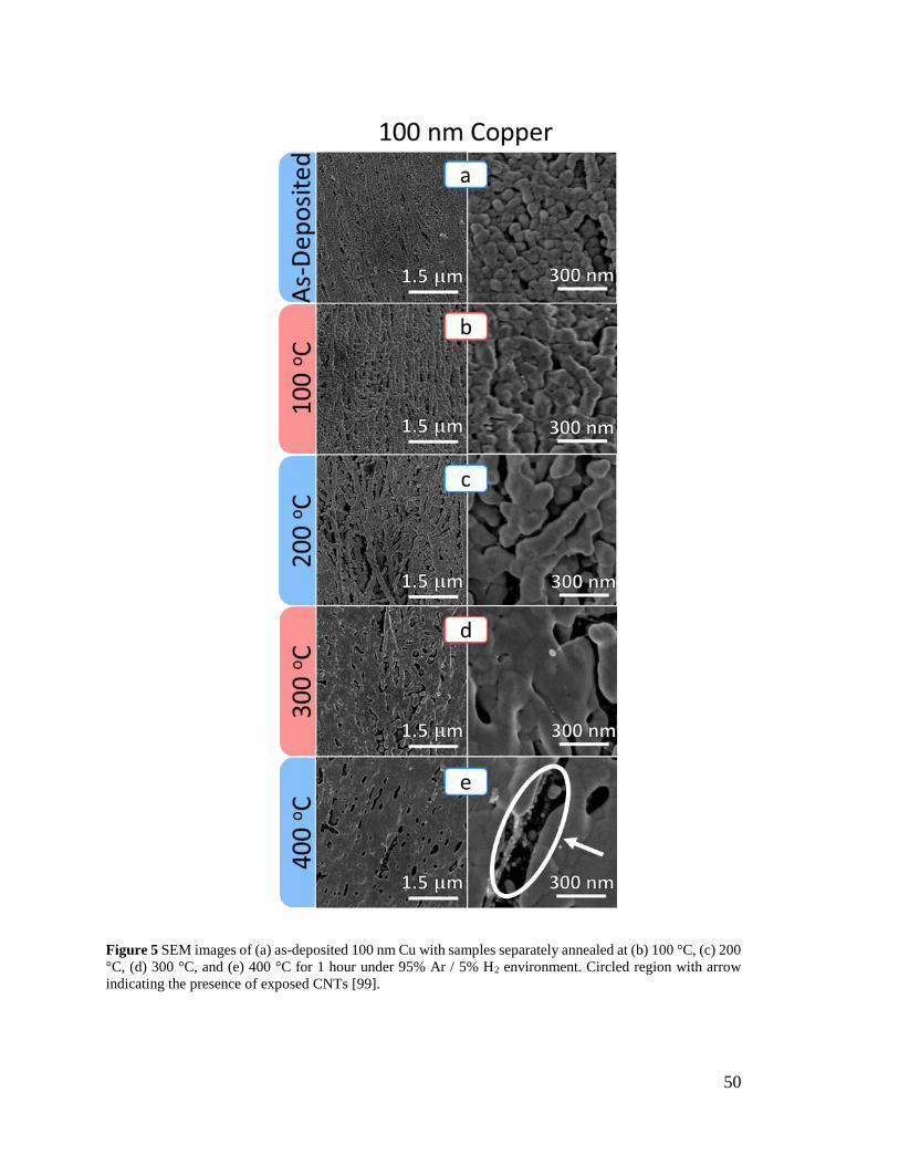
50
Figure 5 SEM images of (a) as-deposited 100 nm Cu with samples separately annealed at (b) 100 °C, (c) 200
°C, (d) 300 °C, and (e) 400 °C for 1 hour under 95% Ar / 5% H2 environment. Circled region with arrow
indicating the presence of exposed CNTs [99].
51
Figure 6 shows SEM images of the CNT conductor after deposition with 10 nm of
Ni thermally evaporated and after a 1 hour anneal in 5% H2 / 95% Ar at different
temperatures. From Figure 6, the gradual formation of discrete structures by the 10 nm
thick Ni can be observed as the temperature is increased to 400 °C. The as-deposited Ni
layer consists of well-distributed nanocrystallites, giving it a textured appearance. The
nanoscale textured surface features have been attributed to fast surface diffusion of
adatoms upon deposition, implying a low diffusion activation energy (i.e. weak binding
energy) characteristic of poor condensate-substrate interaction [65]. As the annealing
temperature is increased to 200 °C, the Ni layer begins to coalesce together. As the
temperature further increases to 300 °C, the layer continues to discretize, and Ni island
formation occurs. At 400 °C, the Ni island formations evolve into larger isolated
particles, which is attributed to Ostwald ripening effects, whereby the Ni atoms reduce
their total interfacial energy with the CNTs via coalescence into larger particles,
minimizing the total surface area due to poor interaction with the CNTs [103]. Such a
phenomenon has previously been observed for nanoscale Ni on TiO2/n-Si substrates,
whereby temperatures as low as 300 to 500 °C were found to induce dispersed island
formation for Ni thicknesses up to 8 nm as a result of Ni atoms being weakly bound to
the substrate [103]. Thus, the textured surface after deposition, combined with the
discrete particle formation observed upon annealing in this study, demonstrate
characteristics of weak binding of Ni with CNTs.

52
Figure 6 SEM images of (a) as-deposited 10 nm Ni with samples separately annealed at (b) 100 °C, (c) 200
°C, (d) 300 °C, and (e) 400 °C for 1 hour under 95% Ar / 5% H2 environment [99].
53
Figure 7 shows SEMs of the samples with 10 nm of Ti thermally evaporated onto
the CNT conductor (and after the 1 hour anneal) at different temperatures. The SEM of
the as-deposited Ti layer shows that the CNT bundles are uniformly coated when
compared to the starting CNT conductor. The presence of sparse particulates is attributed
to the residual iron catalyst present on the as-received CNT conductor as highlighted in
Figure 1. In contrast with the observations made with the Ni deposition, the Ti layer does
not exhibit visible surface irregularity upon deposition. In addition, it remains uniform
upon annealing. No observable differences can be made between the Ti coating as-
deposited and after annealing, suggesting favorable adhesion properties. The evolution of
the coating upon exposure to temperatures up to 400 °C reveal important insight toward
the effectiveness of the adhesion layers as part of conductors that will be subjected to
elevated temperatures.

54
Figure 7 SEM images of (a) as-deposited 10 nm Ti with samples separately annealed at (b) 100 °C, (c) 200
°C, (d) 300 °C, and (e) 400 °C for 1 hour under 95% Ar / 5% H2 environment, showcasing sustained
uniformity [99].
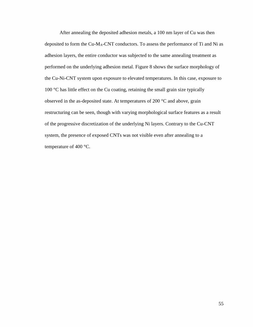
55
After annealing the deposited adhesion metals, a 100 nm layer of Cu was then
deposited to form the Cu-MA-CNT conductors. To assess the performance of Ti and Ni as
adhesion layers, the entire conductor was subjected to the same annealing treatment as
performed on the underlying adhesion metal. Figure 8 shows the surface morphology of
the Cu-Ni-CNT system upon exposure to elevated temperatures. In this case, exposure to
100 °C has little effect on the Cu coating, retaining the small grain size typically
observed in the as-deposited state. At temperatures of 200 °C and above, grain
restructuring can be seen, though with varying morphological surface features as a result
of the progressive discretization of the underlying Ni layers. Contrary to the Cu-CNT
system, the presence of exposed CNTs was not visible even after annealing to a
temperature of 400 °C.
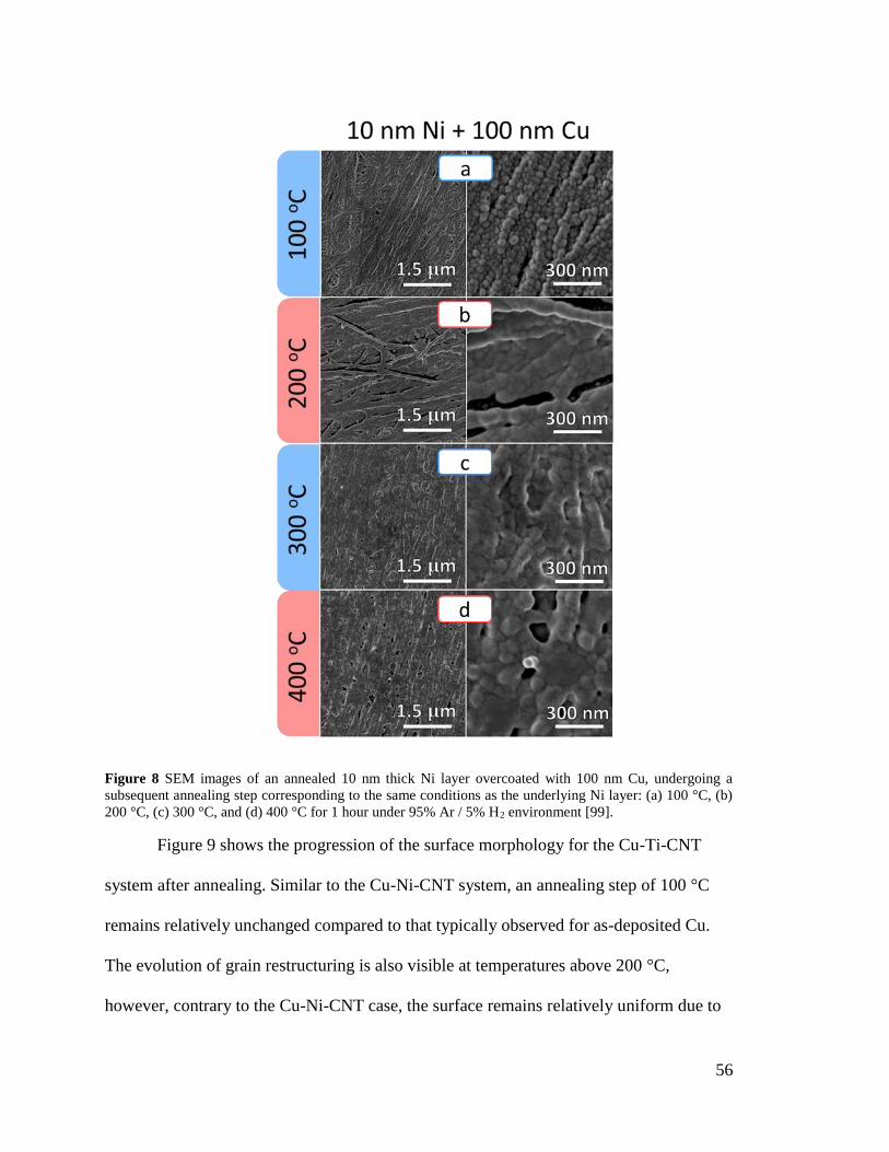
56
Figure 8 SEM images of an annealed 10 nm thick Ni layer overcoated with 100 nm Cu, undergoing a
subsequent annealing step corresponding to the same conditions as the underlying Ni layer: (a) 100 °C, (b)
200 °C, (c) 300 °C, and (d) 400 °C for 1 hour under 95% Ar / 5% H2 environment [99].
Figure 9 shows the progression of the surface morphology for the Cu-Ti-CNT
system after annealing. Similar to the Cu-Ni-CNT system, an annealing step of 100 °C
remains relatively unchanged compared to that typically observed for as-deposited Cu.
The evolution of grain restructuring is also visible at temperatures above 200 °C,
however, contrary to the Cu-Ni-CNT case, the surface remains relatively uniform due to
57
the enhanced adhesion of the Ti layer at all temperatures. The Cu-CNT system without
the use of an adhesion layer demonstrates poor interaction at annealing temperatures of
400 °C, as film gap formation occurs, exposing underlying CNTs (see Figure 5e). In the
case of both Ni and Ti adhesion layers, however, suppression of significant Cu
delamination is observed, with no underlying CNTs exposed, demonstrating improved
bonding between the Cu overcoat and the CNT conductor.
Figure 9 SEM images of an annealed 10 nm thick Ti layer overcoated with 100 nm Cu, undergoing a
subsequent annealing step corresponding to the same conditions as the underlying Ti layer: (a) 100, (b) 200,
(c) 300, or (d) 400 °C for 1 hour under 95% Ar / 5% H2 environment [99].

58
Electrical Performance
Physical analysis via SEM shows clear changes in nanoscale morphology for the
metal-CNT conductors upon exposure to the elevated temperatures, and the impact of
those effects on electrical transport is measured via four-point probe measurements. The
CNT conductor material starts with an average resistance per length (R/L) of ~ 340 Ω m-1
and increases by 8.8% after annealing at 400 °C, as seen in Figure 10. It is observed that
the deposition of Cu always decreases the R/L of the conductor, as observed without the
presence of an adhesion metal. Upon deposition of a 100 nm Cu layer, the R/L of Cu-
CNT hybrid reduces to 140 Ω m-1. However, due to the poor interaction between the Cu
film and the underlying CNT conductor, there is an irreversible increase in room
temperature resistance from 140 Ω m-1 to 200 Ω m-1 (40% increase) upon annealing up to
400 °C (see Figure 10). The increase in electrical resistance is attributed to the presence
of gaps generated via the annealing process as observed in Figure 2e, inducing
discontinuous conduction pathways [60]. Nevertheless, in all cases, this is an
improvement from the as-received CNT conductor and provides a benchmark by which
the electrical performance of the adhesion metals used in this study may be compared.
The resistance of the metal-CNT conductor is influenced by the width of the
deposited metal layer, which is dependent on the width of the starting conductor.
Therefore, the R/L values are corrected based on width measurements for each sample to
ensure that the samples are directly comparable. The corrected R/L values reported for
the Cu-CNT conductors have an average standard deviation of 4.6% based on
measurements taken across 2-4 samples fabricated and treated under the same conditions.
59
Figure 10 also shows that prior to Cu deposition, the R/L of the MA-CNT system
is similar to that of the as-received CNT conductor, with the anneal temperature having
no significant effect (~2% variation). The presence of a 10 nm metal layer is not
sufficient to strongly influence the electrical properties of the conductor due to the bulk
conductivity of the metals. The small difference observed between the two adhesion
metals prior to Cu deposition likely arises due to Ni having an order of magnitude greater
conductivity than Ti in bulk form (1.43 × 10⁷ and 2.38 × 10⁶ S m-1, respectively).
The deposition of 100 nm of Cu onto the CNT conductors leads to a decreased
R/L compared to that achieved from the as-deposited adhesion metals. The inclusion of a
10 nm Ni adhesion layer to form a Cu-Ni-CNT hybrid results in a slight decrease in the
as-deposited R/L compared to the Cu-CNT conductor, as seen in Figure 10. However, the
measured R/L of the Cu-Ni-CNT hybrid increases continuously after each anneal for
temperatures up to 300 °C, followed by a sharp increase in R/L up to 309 Ω m-1 around
400 °C. The R/L values reported for the Cu-Ni-CNT hybrids have an average standard
deviation of 6.2%.
In the case of a 10 nm Ti adhesion layer to form a Cu-Ti-CNT hybrid, a higher as-
deposited R/L is observed than the as-deposited Cu-CNT conductor. On the other hand,
the measured R/L of the Cu-Ti-CNT hybrid decreases after exposure to any elevated
temperature, stabilizing around 166 Ω m-1 after being annealed to 200 °C. The R/L values
reported for the Cu-Ti-CNT hybrids have an average standard deviation of 5.3%.
Furthermore, the Cu-Ti-CNT conductor exhibits lower R/L than the Cu-CNT conductor
after exposure to 400 °C, likely due to Cu grain expansion enabled by favorable
adhesion. These results are supported by the observations made in Figure 7 and Figure 9,
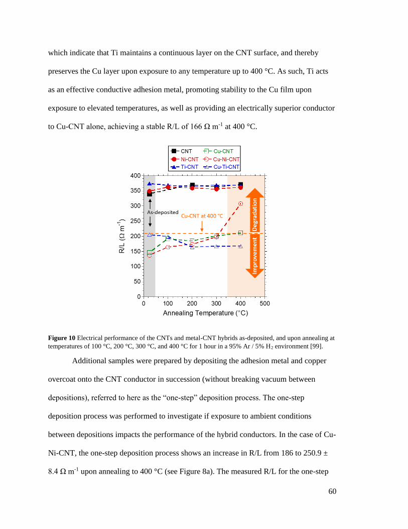
60
which indicate that Ti maintains a continuous layer on the CNT surface, and thereby
preserves the Cu layer upon exposure to any temperature up to 400 °C. As such, Ti acts
as an effective conductive adhesion metal, promoting stability to the Cu film upon
exposure to elevated temperatures, as well as providing an electrically superior conductor
to Cu-CNT alone, achieving a stable R/L of 166 Ω m-1 at 400 °C.
Figure 10 Electrical performance of the CNTs and metal-CNT hybrids as-deposited, and upon annealing at
temperatures of 100 °C, 200 °C, 300 °C, and 400 °C for 1 hour in a 95% Ar / 5% H2 environment [99].
Additional samples were prepared by depositing the adhesion metal and copper
overcoat onto the CNT conductor in succession (without breaking vacuum between
depositions), referred to here as the “one-step” deposition process. The one-step
deposition process was performed to investigate if exposure to ambient conditions
between depositions impacts the performance of the hybrid conductors. In the case of Cu-
Ni-CNT, the one-step deposition process shows an increase in R/L from 186 to 250.9 ±
8.4 Ω m-1 upon annealing to 400 °C (see Figure 8a). The measured R/L for the one-step

61
process is also higher than the Cu-CNT conductor exposed to the same conditions,
demonstrating the detrimental behavior of the Ni/Cu combination. The initial R/L of the
Cu-Ti-CNT samples prepared using the one-step process are lower than those fabricated
with a break in vacuum in-between deposition steps (see Figure 8b). However, after
annealing to 400 °C, the final R/L still maintains 157.9 ± 11.1 Ω m-1, in line with the
results observed for the two-step deposition. Thus, the annealing process in a reducing
environment at 400 °C is sufficient to reconcile any impact on the electrical properties
induced by exposure to the atmosphere (e.g. formation of surface oxides) between
deposition steps.
Figure 11 Electrical measurements comparing the two-step and one-step deposition processes as-deposited
(black) and after annealing to 400 °C (red) for the (a.) Cu-Ni-CNT and (b.) Cu-Ti-CNT hybrids [99].
Temperature-dependent measurements of the resistance of the constructed hybrids
were performed under vacuum at a constant up-ramp rate of 3.3 C min-1 in order to assess
their stability and variability after deposition. Measuring the resistance at incremental
temperatures provides complementary data to understand the dynamic changes in

62
electrical behavior compared to measurements after the static annealing conditions in
Figure 10.
Figure 12 shows the 1st and 2nd cycle temperature-dependent resistance
measurements for the CNT conductors. The resistance values are normalized to the
starting resistance (R/R0) at 26.85 °C (300 K) and show the relative change as a function
of temperature. Two cycles were measured to assess any permanent effects in conductor
transport due to exposure to higher temperatures. The measured R/R0 of the as-received
CNT conductor shows a non-linear behavior (see Figure 9a), as reported previously for
the complex CNT electronic behavior between resistivity and temperature [104]. The 2nd
cycle demonstrates that the as-received CNT response undergoes no change during the up
and down ramps indicating that the sample has stabilized. The observed increase in as-
received CNT starting resistance from the 1st to 2nd cycle is attributed to the reversible
desorption of oxygen or other ambient dopants, after exposure to elevated temperatures,
which directly influences the CNT electronic transport [105–107].
In the case of the Cu-CNT conductor (Figure 12b), the starting resistance of the
2nd cycle shows little variation from that of the 1st cycle. The lack of change under
vacuum may be attributed to the presence of a CuO passivation layer, as there is no
evidence suggesting that the film will coalesce into larger grains leading to more discrete
particles (and increase in R/L) as compared to the annealing studies above. Additionally,
the positive linearity in the slope is typical of metals, as increasing the temperature
increases phonon activity, decreasing the mean-free-path of electrons, thereby increasing
resistance [108].
63
Figure 12c shows the 1st and 2nd cycle data for the Cu-Ni-CNT conductor. The 1st
cycle up-ramp shows a steady increase in resistance until around 270 °C, where the
resistance begins to increase more steeply. The resistance returns to a starting resistance
that is 14% higher than the starting resistance of the 1st cycle. The permanent increase in
resistance upon annealing in vacuum is consistent with the trend observed for the
annealing measurement data presented in Figure 10, rendering Ni an ineffective adhesion
metal in Cu-Ni-CNT conductors exposed to elevated temperatures in either vacuum or
reducing environments.
Figure 12d shows the temperature-dependent measurements for the Cu-Ti-CNT
conductor. During the 1st cycle, a steady increase in resistance up to ~ 270 °C is
observed, however, in contrast with Cu-Ni-CNT, the slope of the resistance begins to
reverse as the temperature goes to 327 °C (600 K). The resistance steadily decreases to a
starting resistance that is 12% lower than the starting resistance of the 1st cycle. The
ability of Ti as an adhesion metal to provide a permanent decrease in room temperature
resistivity when subjected to elevated temperatures in a reducing atmosphere is
complemented by the measurements conducted under vacuum, whereby the resistivity of
Cu-Ti-CNT conductors decreases between the 1st and 2nd cycle, further validating the
benefit of Ti as an adhesion metal in elevated temperature applications.
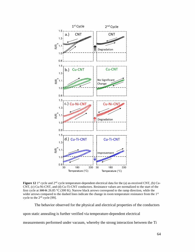
64
Figure 12 1st cycle and 2nd cycle temperature-dependent electrical data for the (a) as-received CNT, (b) Cu-
CNT, (c) Cu-Ni-CNT, and (d) Cu-Ti-CNT conductors. Resistance values are normalized to the start of the
first cycle at 300 K 26.85 °C (300 K). Narrow black arrows correspond to the ramp direction, while the
wider arrows compared to the dashed lines indicate the change in room temperature resistance from the 1st
cycle to the 2nd cycle [99].
The behavior observed for the physical and electrical properties of the conductors
upon static annealing is further verified via temperature-dependent electrical
measurements performed under vacuum, whereby the strong interaction between the Ti

65
and the CNTs results in a reduction in room temperature resistance from the first cycle to
the second cycle. The performance observed for the hybrids fabricated here can be
explained by the interaction expected between the various metals and the CNTs. Previous
studies have suggested that metals with a higher amount of vacancies in the d-orbital
react more readily with carbon [66], and thus exhibit better wettability on CNTs [79].
Since Cu has a full d-orbital, it exhibits the worst interaction with carbon. Ni exhibits
improved characteristics over that of Cu, due to having two d-orbital vacancies, however,
still exhibits weaker interaction with CNTs than Ti, forming quasicontinuous coatings
(when < 5 nm thick) as-deposited onto individual CNTs [63]. Ti exhibits the strongest
reactivity (of the three metals investigated here) with carbon owing to its eight d-orbital
vacancies [66]. Moreover, computational studies have calculated that Ti has a high
binding energy with CNTs of various chiralities [90, 109], which supports the formation
of continuous Ti chains on the surface [90], corroborating experimental findings of the
tendency of Ti to wet individual CNTs [63, 64]. It has been suggested that the high
binding energy calculated between Ti and CNTs may stem from hybridization of the 3d
orbitals of the Ti with the 2p orbitals of carbon, as the 3d orbitals in Ti tend to behave as
valence orbitals facilitating bonding [90, 110, 111]. The weakness/strength of these
interactions are also evidenced here by the textured nanostructure morphology of as-
deposited Ni (Figure 6a), and the uniform coating of the as-deposited Ti (Figure 7a),
respectively. While fast surface diffusion accompanied by low nucleation rate are
responsible for the formation of surface roughness upon deposition, a conformal coating
corresponds to a strong binding energy and condensation coefficient between the metals
and the CNTs [64].
66
The electrical properties of the conductors also reveal insight toward the metal-
CNT interaction. While Ni exhibits weaker interaction with carbon than Ti, it is capable
of providing some benefit to the electrical properties in a Cu-Ni-CNT conductor over that
of Cu-CNT alone when exposed to temperatures up to 300 °C in a reducing environment.
At temperatures of 400 °C, however, degradation is observed in the electrical benefits of
the Cu-Ni-CNT conductor, as the resistance sharply increases beyond that of the Cu-
CNT. The sharp rise in resistance may be attributed to the fact that the Ni layer on its
own minimizes its area on the surface of the CNTs at this temperature, thereby exposing
bare CNT surface prior to the Cu deposition as observed in Figure 6. Furthermore, the Ni
may be negatively impacting the CNT structure due to the high carbon solubility [45].
Additionally, the Cu and Ni are likely forming a low concentration Ni/Cu alloy which is
also contributing to an increase in R/L beyond that expected for Cu-CNT alone. It is
known that metallurgically processed [112] and electrodeposited [88] Ni-Cu alloys
experience an increase in resistivity over that of pure Cu as the Ni content is increased.
Moreover, nano-phase Ni-Cu is expected to have a depression in the liquidus and solidus
curves compared to its bulk form [113]. The high surface energy between the CNTs and
the Ni (as indicated by the formation of discrete Ni particles in Figure 6e) may further
reduce the temperatures required to form an alloy. The electrical data presented here
suggests that an alloy may be forming at temperatures as low as 400 °C, which is
detrimental for operation or processing of such metal-CNT hybrids at elevated
temperatures when using Ni as an adhesion metal. In contrast, enhanced interaction
between Ti and the CNT conductor enables the Cu grain structure to expand while
maintaining adhesion. In addition, the material compatibility between Ti and Cu sustains
67
the electrical benefits induced by the annealing to temperatures up to 400 °C. As a result,
the Cu-Ti-CNT conductor outperforms the Cu-CNT and Cu-Ni-CNT conductors upon
exposure to 400 °C, and, therefore, Ti emerges as an effective adhesion metal for metal-
CNT conductors.
In conclusion, interfacing CNTs and Cu with a Ni or Ti layer proves to mitigate
Cu-CNT connectivity problems, providing stability to the Cu overcoat upon exposure to
elevated temperatures. Without the use of an adhesion metal, Cu deposited onto the CNT
conductor coalesces at elevated temperature, which is relevant for motor applications,
and is accompanied by an irreversible increase in resistance. Ni showed poor adhesion to
the CNTs at elevated temperatures, however, the use of Ni in a Cu-Ni-CNT system
suppressed the delamination of the Cu layer. The electrical properties, however, were still
unfavorable at temperatures reaching 400 °C, ultimately increasing resistance by up to
125%. In the case of Ti, on the other hand, uniformity of the coating was preserved upon
heat treatment, and with the addition of a Cu overcoat, delamination was mitigated. In
addition, the conductive properties of the Cu overcoat in the Cu-Ti-CNT conductor
improved upon annealing, with room temperature resistances decreasing by up to 12%.
Furthermore, temperature-dependent electrical measurements performed under vacuum
demonstrate similar trends as seen in the static anneals in a reducing atmosphere. As a
result, Ti has been identified as an effective interfacing metal for metal-CNT conductors,
which when exposed to elevated temperatures (either through operation or processing),
can provide superior electrical and adhesion benefits, enabling a path forward for
conductor designs.

68
4 Fabrication of Composites Through CVD &
Electrodeposition
Ti is known to exhibit excellent interfacial interaction with CNTs and enhances the
electrical performance for Cu-CNT hybrids. A simple route for depositing Ti to form
integrated Ti-CNT bulk conductors is warranted to increase the total metal:CNT
interfacial contact area. Delivery of Ti rich films is difficult due to the high reactivity of
Ti. Physical vapor deposition techniques offer a facile route toward deposition of pure Ti;
however, these techniques deposit material primarily in the line-of-sight, resulting in
surface coatings. Chemical vapor deposition, on the other hand, is known for its
capability in providing more uniform coverage across irregular topographies [52], and is
suitable for penetrating porous networks [27]. Leggiero et al. have demonstrated the
successful deposition of metals on CNTs using a Joule-heating CVD technique, whereby
a CNT substrate is resistively heated to provide thermal energy sufficient for
decomposition of organometallic precursors [27]. Among the commercially available
CVD precursors, cyclopentadienyl(cycloheptatrienyl) titanium (II) [CHT-Ti-Cp] has been
demonstrated to have the potential to form Ti rich films (24). A potential fragmentation
pathway of the C7H7 and C5H5 rings can occur, in which a disproportionation results in
Objectives
— Identify a viable Ti precursor for CVD delivery.
— Assess Interaction of Ti Deposited via CVD.
— Electroplate to form Cu-Ti-CNT hybrids.
— Optimize metal depositions for high conductivity and favorable TCR.
69
two stable benzene rings being eliminated in turn from the parent ion (24,25). The
research herein reports the utilization of the Joule-heating CVD technique to fabricate
integrated Ti-CNT conductors, whereby the Ti is assessed as an adhesion metal for bulk
Cu-CNT conductors. Delivery of Ti via CVD enables the penetration of Ti into the CNT
network, maximizing the metal:CNT interfacial contact area in the bulk conductor. The
following work in this section has been reprinted with permission from (McIntyre, D. J.,
et al, Integrated Titanium-Carbon Nanotube Conductors via Joule-Heating Driven
Chemical Vapor Deposition, ECS Transactions 97.7 (2020): 321-327). Copyright (2020)
ECS https://doi.org/ 10.1149/09707.0321ecst.
4.1 Fabrication of Ti-CNT Conductors Using Joule-heating Driven CVD
4.1.1 CVD experimental setup
Fabrication and processing
The CNT conductor used in this study is Miralon® roving (lot 954738) obtained
from Nanocomp Technologies Inc. (a Huntsman International LLC. company). This free-
standing unspun CNT conductor takes a ribbon geometry (~30 µm × 1.53 mm), and the
full physical characteristics have been reported previously [27, 99]. A one-hour vacuum
dry at 100 °C is performed on the CNT conductor prior to analysis and processing.
Joule-heating driven chemical vapor deposition (CVD) was performed in
accordance to a previous study [27]. Flat Cu clips crimped to Cu electrical leads are
passed through rubber septa at two opposing necks in a three-neck flask. Three 12 cm
long CNT conductors are suspended in parallel by the Cu clips, sharing a common
electrical contact point at each clip. Precursor masses of 1 mg, 5 mg, and 25 mg
cyclopentadienyl(cycloheptatrienyl) Titanium(II) (CAS# 51203-49-7, Strem Chemicals

70
99%), were loaded into the bottom of the flask within a glovebox, in an inert Ar
atmosphere. A heating mantle temperature of 200 °C was used to sublimate the precursor.
The center neck of the flask was connected to a Schlenk line via a hose-barb adapter with
a stopcock, which allowed for pulling vacuum or supplying 5% H2 / 95% Ar (mol/mol)
gas. A constant current of 350 mA per CNT conductor is continuously applied for one
hour while the precursor is subliming, to provide sufficiently high temperatures required
for decomposing the metal-organic precursor upon contact with the CNTs. A target
vacuum pressure of 0.3 Torr was regulated by opening the stopcock as needed. The Ti-
CNT conductors were then subjected to a 95% Ar / 5 % H2 anneal in a tube furnace at a
temperature of 300 °C for one hour.
Electroplating in a sandwich cell configuration was performed as reported
previously [27] on the 5 mg CHT-Ti-Cp seeded CNT conductor. A constant-current
condition of 7.4 A/gCNT was applied for 354 minutes to achieve a target total metal mass
of 98% wt/wt. Due to irregularities in surface area, plating rate is calculated based on
mass of the CNT conductor. To determine the amount of mass/length needed to be added
in the form of Cu to obtain 98% total metal mass, the following equation is used:
(𝑀
𝐿)𝐴𝑑𝑑𝑒𝑑_𝐶𝑢
=(𝑀
𝐿)𝐴𝑠−𝑟𝑒𝑐𝑒𝑖𝑣𝑒𝑑_𝐶𝑁𝑇𝑠
0.02− (
𝑀
𝐿)𝑇𝑖−𝐶𝑁𝑇_𝐶𝑜𝑚𝑝𝑜𝑠𝑖𝑡𝑒
(7)
The chosen plating rate then determines how much time is necessary to achieve the target
amount of added Cu mass. After electroplating, the Cu-Ti-CNT conductor was then
densified to a target 30 µm using a rolling mill, and subsequently subjected to a 95% Ar /
5 % H2 anneal in a tube furnace at a temperature of 300 °C for three hours.

71
Characterization
Analysis of deposition morphologies was performed using a Hitachi S-4000
scanning electron microscope (SEM) equipped with a secondary electron detector and 10
kV accelerating voltage. Cross-sections for the Cu-Ti-CNT samples were prepared via
razorblade sectioning of the conductors. Energy dispersive X-ray measurements were
performed on the 25 mg CHT-Ti-Cp deposited sample using a Tescan Mira3 SEM
equipped with a Bruker XFlash 6|30 EDS at a 20 kV accelerating voltage. Cross-sections
for EDS mapping were epoxy-set and ultramicrotomed. The room temperature electrical
properties of the conductors were measured in an ambient atmosphere by applying
current-voltage sweeps (up to 100 mA) using a four-point-probe configuration with a
National Instruments NI PXI-5652 source/measure unit and NI PXI-4071 digital
multimeter. Temperature-dependent electrical measurements were performed by
sweeping the temperature from 300 to 600 K under 10-6 mbar vacuum in a Janis cryostat.
Four-point probe I-V sweeps were carried out at 5 K increments for two cycles of
temperature sweeps. Measurements were acquired using a National Instruments NI PXI-
4110 programmable power supply and NI PXI-4072 digital multimeter. The temperature
coefficient of resistance (TCR) was calculated based on the average slope of resistance
with respect to temperature, whereby the resistance is normalized to the starting
resistance at 300 K. TCR calculations are based on the second cycle data. Mass
measurements were made using a Mettler Toledo XP-2U microbalance.
4.1.2 CVD deposited Ti properties
CHT-Ti-Cp
The surface-view SEM image acquired in Figure 13a shows the network
morphology of the starting CNT conductor. A loose network morphology is observed
72
with the presence of nanoscale pores. Joule-heating driven CVD was performed using 25
mg of CHT-Ti-Cp precursor, leading to an average deposition mass loading of 67.2 ±
2.5% wt/wt. The standard deviation reported here is based on three samples fabricated
together at the same conditions. As shown in Figure 13b, a fully connected film forms at
the surface of the Ti-CNT conductor at this mass loading. An ultramicrotomed epoxy-set
cross-section of the Ti-CNT conductor is shown in Figure 13c, with the corresponding
EDS Ti signal overlay shown in Figure 13d. A higher concentration of Ti localizes at the
surface and is likely resultant of deposited Ti blocking the pores at the surface,
preventing further penetration as the CVD process evolves. However, Ti is observed to
be present throughout the entire cross-section of the conductor, indicating successful
penetration of the precursor during the initial stages of the CVD process. Additionally, a
strong Ti peak is observed in the surface-view EDS data (Figure 13e), demonstrating the
successful deposition of Ti. The presence of O is also observed, which may result from
residual adsorbed oxygen within the CNT network, or the formation of surface oxides
after exposure to atmosphere. The oxygen content may be reduced by performing a heat-
treatment to the CNT network, which is known to desorb oxygen and other ambient
dopants [105]. Furthermore, surface oxidation may be minimized by performing a
subsequent CVD deposition using Cu to passivate the Ti surface and improve the Cu-Ti
interface. Nevertheless, the Joule-heating driven CVD technique utilized here has shown
to successfully deposit Ti, and achieve penetration throughout the entirety of the bulk
CNT network.
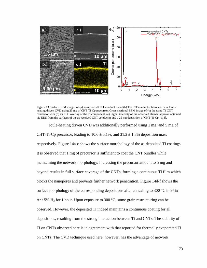
73
Figure 13 Surface SEM images of (a) as-received CNT conductor and (b) Ti-CNT conductor fabricated via Joule-
heating driven CVD using 25 mg of CHT-Ti-Cp precursor. Cross-sectional SEM image of (c) the same Ti-CNT
conductor with (d) an EDS overlay of the Ti component. (e) Signal intensity of the observed elemental peaks obtained
via EDS from the surfaces of the as-received CNT conductor and a 25 mg deposition of CHT-Ti-Cp [114].
Joule-heating driven CVD was additionally performed using 1 mg, and 5 mg of
CHT-Ti-Cp precursor, leading to 10.6 ± 5.1%, and 31.3 ± 1.8% deposition mass
respectively. Figure 14a-c shows the surface morphology of the as-deposited Ti coatings.
It is observed that 1 mg of precursor is sufficient to coat the CNT bundles while
maintaining the network morphology. Increasing the precursor amount to 5 mg and
beyond results in full surface coverage of the CNTs, forming a continuous Ti film which
blocks the nanopores and prevents further network penetration. Figure 14d-f shows the
surface morphology of the corresponding depositions after annealing to 300 °C in 95%
Ar / 5% H2 for 1 hour. Upon exposure to 300 °C, some grain restructuring can be
observed. However, the deposited Ti indeed maintains a continuous coating for all
depositions, resulting from the strong interaction between Ti and CNTs. The stability of
Ti on CNTs observed here is in agreement with that reported for thermally evaporated Ti
on CNTs. The CVD technique used here, however, has the advantage of network
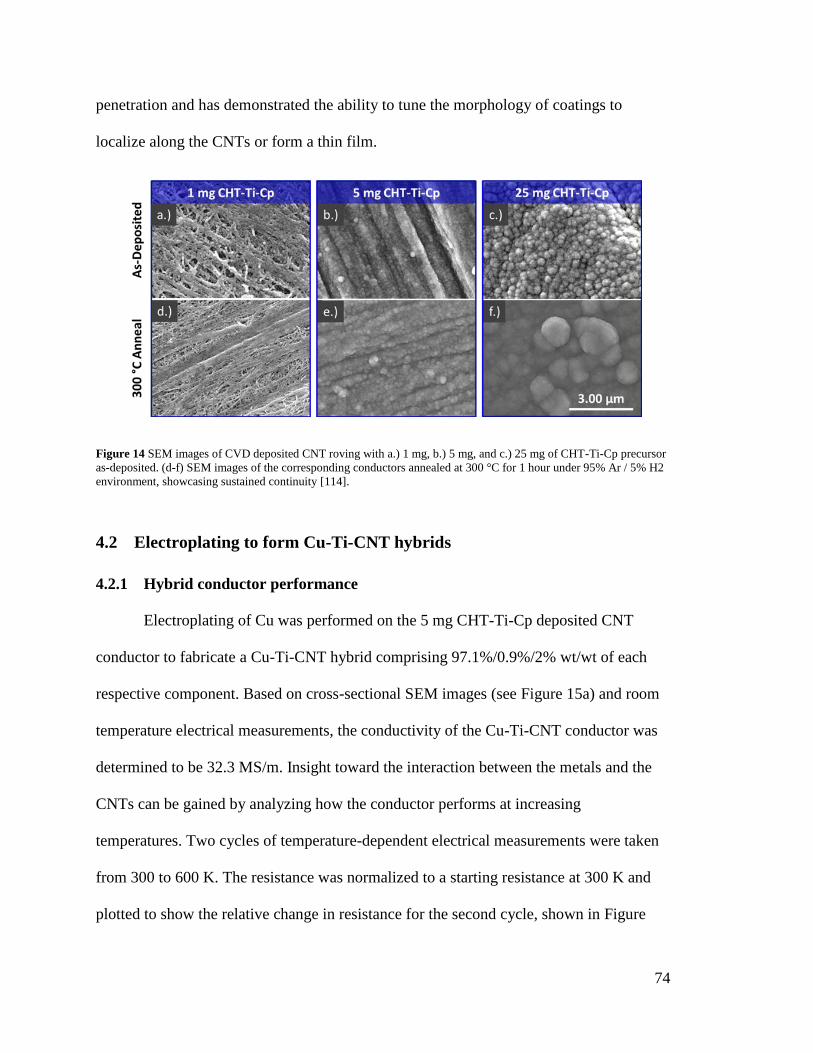
74
penetration and has demonstrated the ability to tune the morphology of coatings to
localize along the CNTs or form a thin film.
Figure 14 SEM images of CVD deposited CNT roving with a.) 1 mg, b.) 5 mg, and c.) 25 mg of CHT-Ti-Cp precursor
as-deposited. (d-f) SEM images of the corresponding conductors annealed at 300 °C for 1 hour under 95% Ar / 5% H2
environment, showcasing sustained continuity [114].
4.2 Electroplating to form Cu-Ti-CNT hybrids
4.2.1 Hybrid conductor performance
Electroplating of Cu was performed on the 5 mg CHT-Ti-Cp deposited CNT
conductor to fabricate a Cu-Ti-CNT hybrid comprising 97.1%/0.9%/2% wt/wt of each
respective component. Based on cross-sectional SEM images (see Figure 15a) and room
temperature electrical measurements, the conductivity of the Cu-Ti-CNT conductor was
determined to be 32.3 MS/m. Insight toward the interaction between the metals and the
CNTs can be gained by analyzing how the conductor performs at increasing
temperatures. Two cycles of temperature-dependent electrical measurements were taken
from 300 to 600 K. The resistance was normalized to a starting resistance at 300 K and
plotted to show the relative change in resistance for the second cycle, shown in Figure
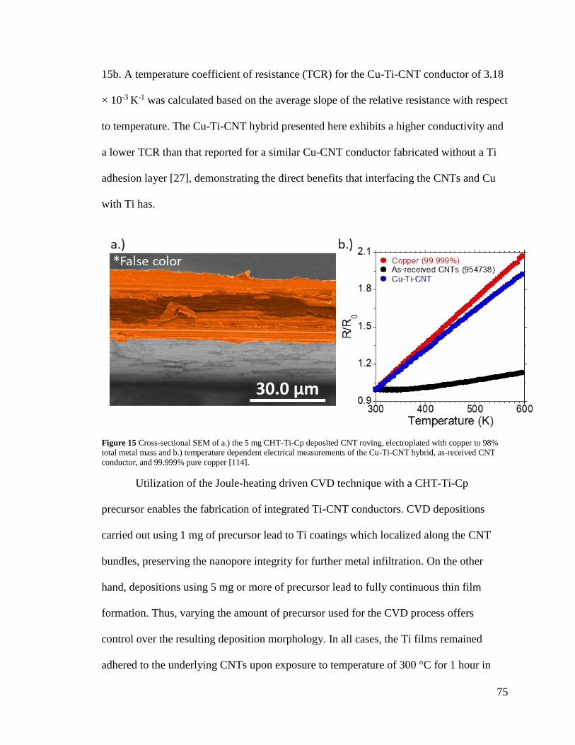
75
15b. A temperature coefficient of resistance (TCR) for the Cu-Ti-CNT conductor of 3.18
× 10-3 K-1 was calculated based on the average slope of the relative resistance with respect
to temperature. The Cu-Ti-CNT hybrid presented here exhibits a higher conductivity and
a lower TCR than that reported for a similar Cu-CNT conductor fabricated without a Ti
adhesion layer [27], demonstrating the direct benefits that interfacing the CNTs and Cu
with Ti has.
Figure 15 Cross-sectional SEM of a.) the 5 mg CHT-Ti-Cp deposited CNT roving, electroplated with copper to 98%
total metal mass and b.) temperature dependent electrical measurements of the Cu-Ti-CNT hybrid, as-received CNT
conductor, and 99.999% pure copper [114].
Utilization of the Joule-heating driven CVD technique with a CHT-Ti-Cp
precursor enables the fabrication of integrated Ti-CNT conductors. CVD depositions
carried out using 1 mg of precursor lead to Ti coatings which localized along the CNT
bundles, preserving the nanopore integrity for further metal infiltration. On the other
hand, depositions using 5 mg or more of precursor lead to fully continuous thin film
formation. Thus, varying the amount of precursor used for the CVD process offers
control over the resulting deposition morphology. In all cases, the Ti films remained
adhered to the underlying CNTs upon exposure to temperature of 300 °C for 1 hour in
76
95% Ar/ 5% H2, demonstrating the strong interaction between the Ti and CNTs. Cu-Ti-
CNT hybrids constructed via electrodeposition of Cu resulted in a high conductivity of
32.3 MS/m and a corresponding TCR of 3.18 × 10⁻³ K-1. Thus, the CVD technique shows
promise as a delivery route for fabricating integrated Ti-CNT conductors for use in high-
performance metal-CNT hybrids.
4.3 CVD and Electroplating Controls
Further optimization has been carried out by performing studies investigating the impact
that metal mass loading has on the room temperature electrical and temperature
dependent electrical performance of the Cu electroplated hybrids.
4.3.1 CVD & Electrodeposition Weight Loading Impact
95% Total Metal Mass / 5 mA Electroplating Current
CVD of CHT-Ti-Cp was performed onto the CNTs as described in 4.1.2 and
electroplated in a sandwich cell configuration with 5 mA cathodic current to a total metal
mass loading of 95% w/w (see Figure 16). Upon planar densification and annealing, the
Cu-Ti-CNT conductors seeded with 5 mg and 25 mg CHT-Ti-Cp exhibited a conductivity
of 1.1 MS/m and 4.9 MS/m, respectively, with TCR300K values of 1.5 and 2.5 × 10⁻³ K-1.
Conductivities were calculated using cross-sectional SEM images to determine the area,
and temperature dependent electrical measurements were performed in the Janis cryostat
as described earlier [114]. Electroplated coatings at 95% total metal mass loading led to
spotty coatings that weren’t well connected at the surface. The lack of sufficient electrical
connection is attributed to the low conductivities obtained at the 95% metal mass loading.
Thus, evaluation of higher electroplated weight loadings are investigated to promote
additional circuitous pathways and enhance the performance of the hybrid conductor.

77
Figure 16 Cross-sectional SEM images of (a) 5 mg, and (b) 25 mg CHT-Ti-Cp deposited CNT roving, electroplated
with Cu to a total metal mass of 95%, using 5 mA current, and further processed by densification, and annealing in 5%
Ar / 95% H2 for 3 hours at 300 °C.
98% Total Metal Mass / 5 mA Electroplating Current
CVD of CHT-Ti-Cp was performed onto the CNTs as described in 4.1.2.
Additionally, a Ti-CNT conductor was fabricated using 0.625 mg of CHT-Ti-Cp
precursor to assess the impact on electrodeposition behavior. As shown in Figure 17, the
deposited Ti with 0.625 mg precursor maintains the network morphology and had greater
retention to the pore structure than achieved at higher weight loadings. Samples were
electroplated in a sandwich cell configuration with 5 mA cathodic current to a total metal
mass loading of 98% w/w (see Figure 18). Electroplating the 0.625 mg CHT-Ti-Cp
seeded conductor (97.9% Cu / 0.1% Ti / 2.0% CNT) led to a surface coating consisting of
gaps and discontinuous regions, resulting in a specific conductivity of 2263 Sm2/k.
Previously, densification has been shown to increase the resistance of the
conductors; however, there exists a trade-off between cross-sectional area and resistance
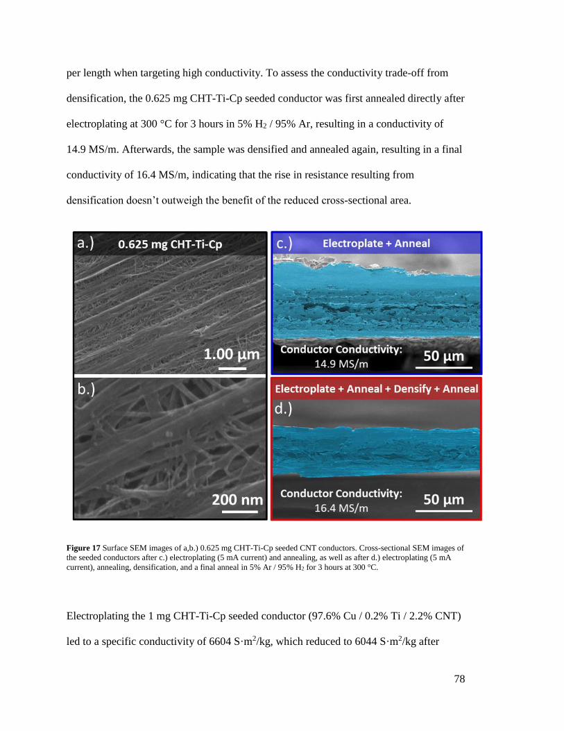
78
per length when targeting high conductivity. To assess the conductivity trade-off from
densification, the 0.625 mg CHT-Ti-Cp seeded conductor was first annealed directly after
electroplating at 300 °C for 3 hours in 5% H2 / 95% Ar, resulting in a conductivity of
14.9 MS/m. Afterwards, the sample was densified and annealed again, resulting in a final
conductivity of 16.4 MS/m, indicating that the rise in resistance resulting from
densification doesn’t outweigh the benefit of the reduced cross-sectional area.
Figure 17 Surface SEM images of a,b.) 0.625 mg CHT-Ti-Cp seeded CNT conductors. Cross-sectional SEM images of
the seeded conductors after c.) electroplating (5 mA current) and annealing, as well as after d.) electroplating (5 mA
current), annealing, densification, and a final anneal in 5% Ar / 95% H2 for 3 hours at 300 °C.
Electroplating the 1 mg CHT-Ti-Cp seeded conductor (97.6% Cu / 0.2% Ti / 2.2% CNT)
led to a specific conductivity of 6604 S·m2/kg, which reduced to 6044 S·m2/kg after
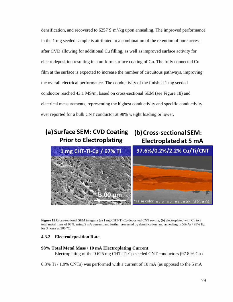
79
densification, and recovered to 6257 S·m2/kg upon annealing. The improved performance
in the 1 mg seeded sample is attributed to a combination of the retention of pore access
after CVD allowing for additional Cu filling, as well as improved surface activity for
electrodeposition resulting in a uniform surface coating of Cu. The fully connected Cu
film at the surface is expected to increase the number of circuitous pathways, improving
the overall electrical performance. The conductivity of the finished 1 mg seeded
conductor reached 43.1 MS/m, based on cross-sectional SEM (see Figure 18) and
electrical measurements, representing the highest conductivity and specific conductivity
ever reported for a bulk CNT conductor at 98% weight loading or lower.
Figure 18 Cross-sectional SEM images a (a) 1 mg CHT-Ti-Cp deposited CNT roving, (b) electroplated with Cu to a
total metal mass of 98%, using 5 mA current, and further processed by densification, and annealing in 5% Ar / 95% H2
for 3 hours at 300 °C.
4.3.2 Electrodeposition Rate
98% Total Metal Mass / 10 mA Electroplating Current
Electroplating of the 0.625 mg CHT-Ti-Cp seeded CNT conductors (97.8 % Cu /
0.3% Ti / 1.9% CNTs) was performed with a current of 10 mA (as opposed to the 5 mA
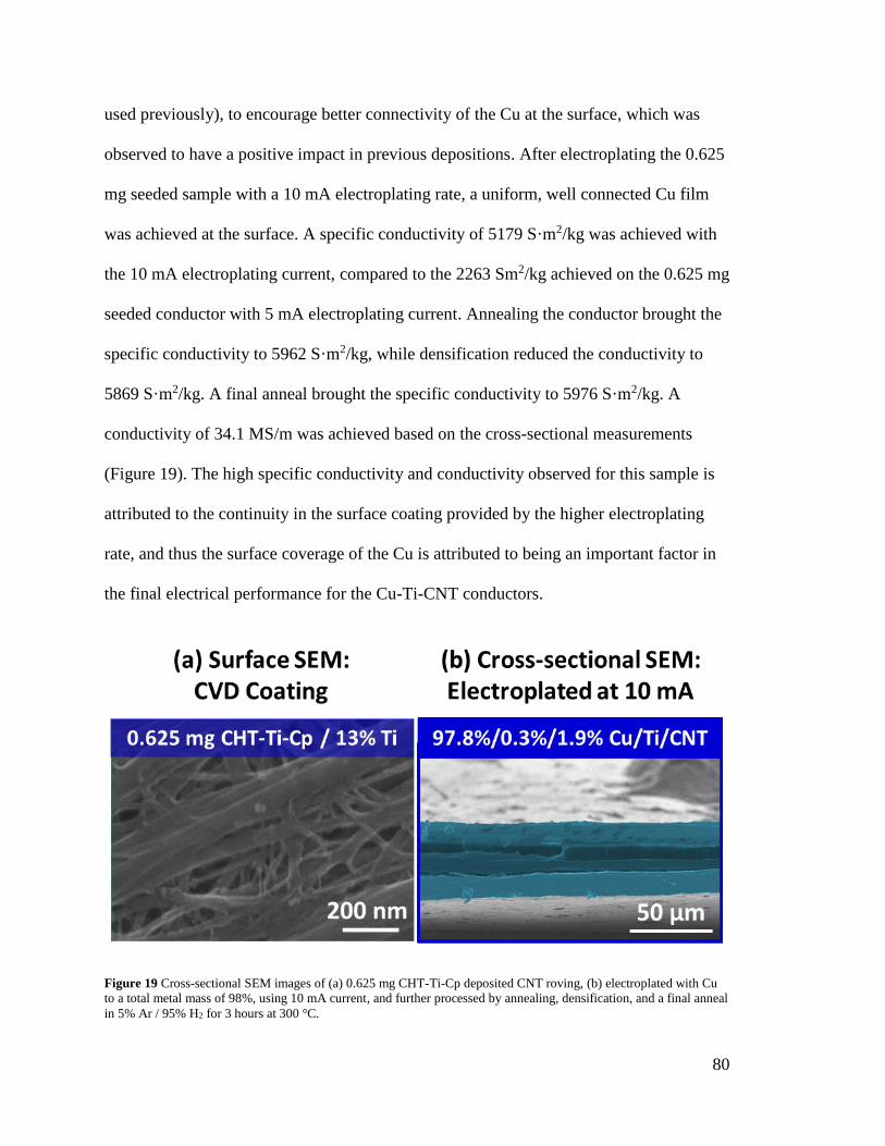
80
used previously), to encourage better connectivity of the Cu at the surface, which was
observed to have a positive impact in previous depositions. After electroplating the 0.625
mg seeded sample with a 10 mA electroplating rate, a uniform, well connected Cu film
was achieved at the surface. A specific conductivity of 5179 S·m2/kg was achieved with
the 10 mA electroplating current, compared to the 2263 Sm2/kg achieved on the 0.625 mg
seeded conductor with 5 mA electroplating current. Annealing the conductor brought the
specific conductivity to 5962 S·m2/kg, while densification reduced the conductivity to
5869 S·m2/kg. A final anneal brought the specific conductivity to 5976 S·m2/kg. A
conductivity of 34.1 MS/m was achieved based on the cross-sectional measurements
(Figure 19). The high specific conductivity and conductivity observed for this sample is
attributed to the continuity in the surface coating provided by the higher electroplating
rate, and thus the surface coverage of the Cu is attributed to being an important factor in
the final electrical performance for the Cu-Ti-CNT conductors.
Figure 19 Cross-sectional SEM images of (a) 0.625 mg CHT-Ti-Cp deposited CNT roving, (b) electroplated with Cu
to a total metal mass of 98%, using 10 mA current, and further processed by annealing, densification, and a final anneal
in 5% Ar / 95% H2 for 3 hours at 300 °C.

81
4.3.3 Temperature Dependent Electrical Behavior
Temperature dependent electrical measurements of the electroplated and fully processed
CHT-Ti-Cp seeded conductors have been conducted under vacuum (10-6 mbar) in the
temperature range of 300 – 600 K (see Figure 20a). Samples electroplated (5 mA current)
to a total metal mass loading of 95% exhibited the lowest TCR300K values for any of the
Cu-Ti-CNT conductors evaluated, at 1.5 and 2.5 × 10⁻³ K-1 for 1 mg and 5 mg CHT-Ti-
Cp seeded conductors respectively. As the weight loading is increased to 98% metal w/w
(at 5 mA current), the TCR values correspondingly increase, attributed to the better
connected surface Cu playing a more prominent role in the electrical transport. TCR300K
values of 3.12, 3.49 and 3.18 × 10⁻³ K-1 were obtained for 0.625, 1, and 5 mg CHT-Ti-Cp
seeded conductors, respectively. Lastly, a TCR300K value of 3.53 × 10⁻³ K-1 was obtained
for the 0.625 mg CHT-Ti-Cp seeded conductor that was electroplated to 98% total metal
mass at 10 mA electroplating current. Due to the extensive processing and measurement
time required for each sample, repeats for exact conditions have not been performed. The
results are thus assessed based on the general trends observed. It is generally observed
here that higher total mass loading as well as higher electroplating rates both lead to more
conductive coatings at the expense of a higher TCR, which is consistent with studies that
have found TCR to be dependent on the amount of filling and intermixing with the
underlying CNTs. Moreover, samples that had a better connected Cu film at the surface
tended to exhibit higher specific conductivities as well as higher TCR values as a result
of the increased participation of the Cu.
In all cases, the TCR is lower for the Cu-Ti-CNT hybrids, and thus a metric is
needed to assess whether the combination of TCR and conductivity indicates a lack of
82
interaction or favorable interaction. To evaluate the performance for conductivity or
specific conductivity, a simple rule of mixtures comparison is sufficient to indicate
whether the electrical performance exceeds that of two non-interacting conductors (i.e.
Cu and CNTs). For assessing the TCR, a model has been developed to calculate an
expected TCR for a non-interacting, parallel resistor combination of CNTs and Cu at any
Cu mass fraction from 0 to 100% [27], as shown in the curve in Figure 20b. The Cu-Ti-
CNT hybrids fabricated here have been plotted against the curve. Conductors with higher
specific conductivity and lower TCR than the curve represent cases where favorable
interaction leads to enhanced electrical properties. It is observed that the samples
fabricated at 95% total mass loading don’t interact well, and instead perform worse than
two independent resistors. Potentially the deposition in these cases led to increased
scattering and were not connected well enough to provide enhancements to the electrical
transport. However, samples with higher mass loading (98%) as well as faster
electroplating rates are observed to exceed the rule of mixtures performance, indicating
enhanced electrical interconnection. In fact, the 1 mg CHT-Ti-Cp seeded conductor has a
specific conductivity of 6257 Sm2/kg, combined with a TCR300K of 3.49 × 10⁻³ K-1, and
thus outperforms pure Cu in terms of specific conductivity at any temperature above 250
°C, demonstrating direct energy savings for elevated temperature applications.

83
Figure 20 (a) Temperature-dependent resistance measurements for the various Cu-Ti-CNT hybrids, as well as (b) a
comparison the TCR versus specific conductivity for the various CHT-Ti-Cp seeded conductors.
84
5 Surface Modification towards Enhanced Ti-CNT Interface
5.1 Contact Modification and Oxidation Prevention
5.1.1 Material Processing: Purification and Joule-heating Annealing
The non-localized electrons in CNTs leads to ambient susceptibility due to van der Waals
attractions at the sidewalls, whereby molecules adsorb out-of-plane to the CNTs [71, 72,
74]. Specifically, moisture and oxygen from the ambient are known to adsorb well to
CNTs [105]. The presence of adsorbed molecules alters the density of states for CNTs
and can negatively impact the contact between metals and CNTs [69]. In fact, previous
work demonstrated that current stressing provides enough Joule-heating to drive off
adsorbed molecules [115, 116], and was separately shown to drastically improve the
contact resistance between CNTs and metals [69]. Thus, the presence of foreign
molecules can strongly influence the overall electrical properties and must be considered
for metal-CNT hybrid conductor design.
In the context of Ti deposition onto CNTs, oxygen removal is especially
important, as Ti is highly reactive and forms non-conductive oxides. In addition to
adsorbed oxygen at the CNT walls, metal catalysts used during the synthesis of CNTs can
also remain trapped within the network and may be susceptible to oxide formation. Such
oxides (e.g. Fe2O3) may undergo a redox reaction with the highly reactive Ti, or
Objectives
— Purify NCTI roving to remove catalyst and improve interaction with CVD deposited
metals.
— Develop control over oxide formation during CVD depositions
— Evaluate the influence of CVD on the electrical properties by modeling the
temperature dependent electrical properties.

85
otherwise alter the contacting properties. Thus, in the pursuit of a Ti-rich film, multiple
sources of oxygen must be considered and managed. As seen in Figure 13e, a non-
negligible oxygen EDS signal is present upon CVD deposition of Ti onto the CNTs.
Since the CHT-Ti-Cp precursor doesn’t inherently contain oxygen, the only source of
oxygen is that within the CNT network, and that from exposure to atmosphere.
Pretreatment steps are employed here to reduce oxygen content and encourage the
deposition of Ti-rich or TiC films. A CNT purification technique has been previously
developed to remove carbonaceous impurities and catalysts [117]. This purification
technique is adapted and optimized for the CNT materials used herein for the removal of
the catalyst to provide a cleaner surface for contacting. The as-received Miralon is loaded
into a tube furnace and ramped to 560 °C at 10 °C/min in air to burn carbonaceous
material and oxidize the metal catalyst, and subsequently submerged in concentrated HCl
for 30 minutes to dissolve the catalyst. A final burn to 560 °C is performed with identical
conditions to the first burn to remove any residual acid. The efficiency of purification is
assessed via thermogravimetric analysis (see Figure 21), from which the residual catalyst
remaining within the CNTs after purification is shown to be < 1.4%. The amount of
catalyst remaining determined by TGA is corroborated with EDX measurements, which
shows <1 % Fe remaining, in close agreement with the TGA data (see Figure 22). It
should also be noted that purification leads to a reduction in the overall mass of the
conductors, reducing the mass/length to ~8 tex, and correspondingly increasing the R/L
to ~350 Ω/m. As such, the thermal response to an electric bias is also altered and must be
accounted for, for use in CVD experiments.
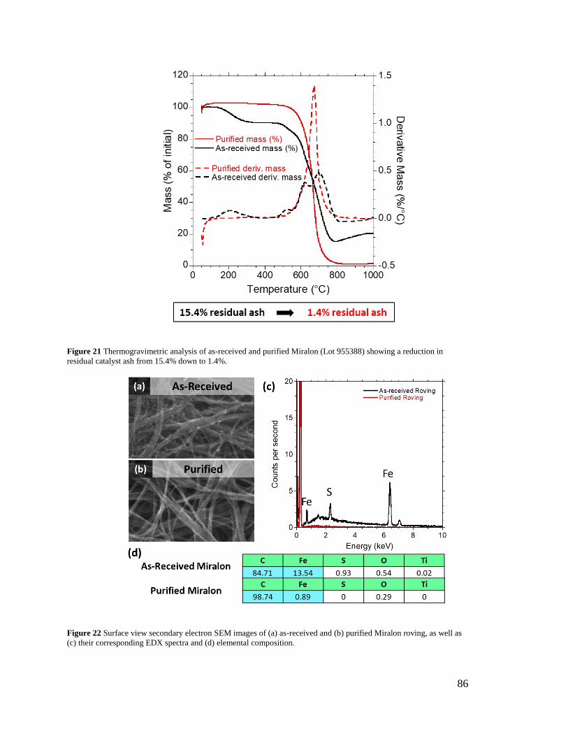
86
Figure 21 Thermogravimetric analysis of as-received and purified Miralon (Lot 955388) showing a reduction in
residual catalyst ash from 15.4% down to 1.4%.
Figure 22 Surface view secondary electron SEM images of (a) as-received and (b) purified Miralon roving, as well as
(c) their corresponding EDX spectra and (d) elemental composition.
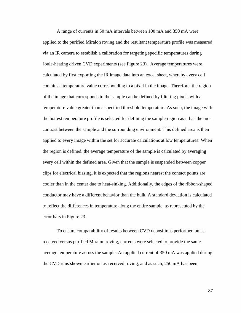
87
A range of currents in 50 mA intervals between 100 mA and 350 mA were
applied to the purified Miralon roving and the resultant temperature profile was measured
via an IR camera to establish a calibration for targeting specific temperatures during
Joule-heating driven CVD experiments (see Figure 23). Average temperatures were
calculated by first exporting the IR image data into an excel sheet, whereby every cell
contains a temperature value corresponding to a pixel in the image. Therefore, the region
of the image that corresponds to the sample can be defined by filtering pixels with a
temperature value greater than a specified threshold temperature. As such, the image with
the hottest temperature profile is selected for defining the sample region as it has the most
contrast between the sample and the surrounding environment. This defined area is then
applied to every image within the set for accurate calculations at low temperatures. When
the region is defined, the average temperature of the sample is calculated by averaging
every cell within the defined area. Given that the sample is suspended between copper
clips for electrical biasing, it is expected that the regions nearest the contact points are
cooler than in the center due to heat-sinking. Additionally, the edges of the ribbon-shaped
conductor may have a different behavior than the bulk. A standard deviation is calculated
to reflect the differences in temperature along the entire sample, as represented by the
error bars in Figure 23.
To ensure comparability of results between CVD depositions performed on as-
received versus purified Miralon roving, currents were selected to provide the same
average temperature across the sample. An applied current of 350 mA was applied during
the CVD runs shown earlier on as-received roving, and as such, 250 mA has been
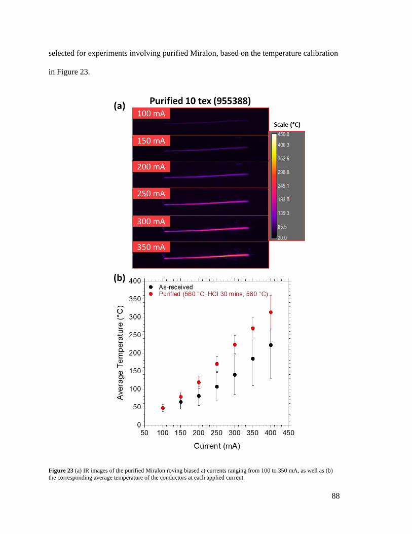
88
selected for experiments involving purified Miralon, based on the temperature calibration
in Figure 23.
Figure 23 (a) IR images of the purified Miralon roving biased at currents ranging from 100 to 350 mA, as well as (b)
the corresponding average temperature of the conductors at each applied current.
89
5.1.2 Vacuum CVD (< 0.250 Torr)
Using a purified CNT template helps to ensure that the impact of the CVD experiments
can be attributed to the deposited metal, and to reduce any unexpected interactions with
catalysts and/or species adsorbed at the surface of the CNTs. Thus, in the remaining
sections, CVD conditions are developed for purified Miralon roving, and the resulting
material properties are assessed via a mixture of electron microscopy, energy dispersive
X-ray spectroscopy, mass and electrical measurements, and Raman spectroscopy.
In this study, an as-received Miralon CNT roving material is subjected to the
purification procedure outline in section 5.1.1 to remove carbonaceous material, and
catalyst metals trapped within the network. After purfication, there is a potential for
oxygen to be adsorbed at the CNT sidewalls and/or bonded through functionalization.
EDX spectroscopy indicates an elemental purity of ~99% carbon after purification;
however, for extra caution, a reducing step is applied to clean the network. An in-situ
hydrogen reduction is performed wherein the CNT network is Joule-heated in a 5%
H2/95% Ar atmosphere for 1 minute to reduce any potential functionalization, followed
by 1 minute under vacuum, with sufficient current to reach temperatures > 300 °C
(shown to drive off ambient dopants during temperature dependent resistance
measurements shown in Figure 12). To monitor the impact of the treatment in-situ,
applied current is increased in 50 mA steps for 1 minute intervals. In between each
interval, the resistance of the sample is measured at 50 mA of applied current to ensure
that the resistance isn’t influenced by temperature during the measurement. The applied
current for reducing the CNTs is increased in 50 mA steps until the room-temperature
resistance is stabilized, indicating that the reaction is finished.
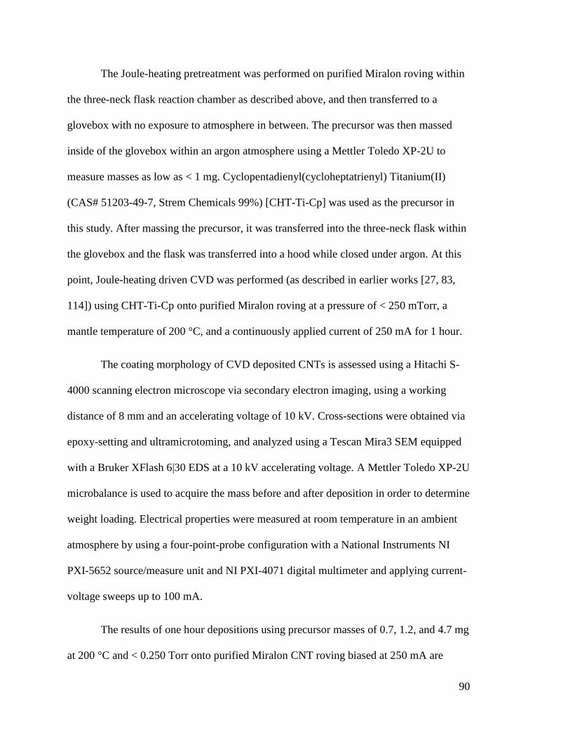
90
The Joule-heating pretreatment was performed on purified Miralon roving within
the three-neck flask reaction chamber as described above, and then transferred to a
glovebox with no exposure to atmosphere in between. The precursor was then massed
inside of the glovebox within an argon atmosphere using a Mettler Toledo XP-2U to
measure masses as low as < 1 mg. Cyclopentadienyl(cycloheptatrienyl) Titanium(II)
(CAS# 51203-49-7, Strem Chemicals 99%) [CHT-Ti-Cp] was used as the precursor in
this study. After massing the precursor, it was transferred into the three-neck flask within
the glovebox and the flask was transferred into a hood while closed under argon. At this
point, Joule-heating driven CVD was performed (as described in earlier works [27, 83,
114]) using CHT-Ti-Cp onto purified Miralon roving at a pressure of < 250 mTorr, a
mantle temperature of 200 °C, and a continuously applied current of 250 mA for 1 hour.
The coating morphology of CVD deposited CNTs is assessed using a Hitachi S-
4000 scanning electron microscope via secondary electron imaging, using a working
distance of 8 mm and an accelerating voltage of 10 kV. Cross-sections were obtained via
epoxy-setting and ultramicrotoming, and analyzed using a Tescan Mira3 SEM equipped
with a Bruker XFlash 6|30 EDS at a 10 kV accelerating voltage. A Mettler Toledo XP-2U
microbalance is used to acquire the mass before and after deposition in order to determine
weight loading. Electrical properties were measured at room temperature in an ambient
atmosphere by using a four-point-probe configuration with a National Instruments NI
PXI-5652 source/measure unit and NI PXI-4071 digital multimeter and applying current-
voltage sweeps up to 100 mA.
The results of one hour depositions using precursor masses of 0.7, 1.2, and 4.7 mg
at 200 °C and < 0.250 Torr onto purified Miralon CNT roving biased at 250 mA are
91
presented in Figure 24. Mass measurements indicate that an increase in metal mass
loading is obtained as the amount of precursor mass is increased, as expected, and is
consistent with that observed for other precursors [27, 83]. Three samples were separately
fabricated for the 4.7 mg condition to assess the reliability of targeting a specific weight
loading using a specified precursor mass. The three samples resulted in a standard
deviation for the weight loading of 4%, demonstrating the reliability of the method, and is
within the range of standard deviations observed for depositions performed onto as-
received Miralon CNTs with varied weight loadings (1.8-5.1%) [114]. All further
depositions are performed on individual samples and the reliability is confirmed through
the observation of consistent trends as established on prior sample sets. SEM imaging
shows that a light coating is deposited using 0.7 mg of precursor, which is localized along
the network morphology and preserves the mesoporous accessibility to an extent. As the
precursor mass is increased to 1.2 mg, thickening of the coating around the bundles is
observed and correspondingly, the void space between CNT bundles begins to fill in. At
4.7 mg, a fully connected film coats the CNT network, and the network morphology is no
longer visible. As such, tunability of the coating morphology is demonstrated.
Additionally, the Ti coating is observed to be uniform and continuous in all cases, with
no observation of discrete crystallite formation, owing to its favorable interaction with
CNTs.
92
Figure 24 (a) Plot of the weight loading %w/w versus the starting precursor mass for CHT-Ti-Cp depositions
performed at < 0.250 Torr, with a 200 °C mantle temperature, and 250 mA applied current for 1 hour. SEM images
showing the morphology of the corresponding depositions with (b) 0.7 mg, (c) 1.2 mg, and (d) 4.7 mg CHT-Ti-Cp
precursor.
93
Raman spectroscopy was performed to assess the characteristics of the hybrids
after deposition. After CVD was conducted, samples were transported in glass vials held
under an argon environment and sealed with Parafilm to prevent exposure to the
atmosphere. Samples were subject to only minutes of exposure to atmospheric conditions
while the Raman measurements were actively being taken. The measurements obtained
via Raman spectroscopy show the standard graphitic peak at 1583 cm-1 associated with
sp2-bonded carbon, as well as a defect peak at 1331 cm-1 associated with sp3-bonded
carbon. Additionally, peaks are observed to be present that are identified for TiO2 at
locations of 218, 440, and 604 cm-1, compared to those reported at 219, 443, and 609 cm-
1. Given that the precursor itself contains no oxygen, and the CNT network is treated to
provide > 99% carbon purity, it is hypothesized that the reactor chamber is susceptible to
trace amounts of oxygen insertion during the experiment at the inlets of the rubber setpa
whereby the electrical leads are passed through. To ensure an oxygen-free environment,
modifications to the reactor set-up were investigated.

94
Figure 25 Raman spectroscopy measurements of a 5 mg CHT-Ti-Cp deposition onto purified Miralon CNT roving
performed at < 0.250 Torr, with a 200 °C mantle temperature, and 250 mA applied current for 1 hour.
The standard three-neck flask set-up was modified to accommodate pressures greater
than atmosphere, allowing for a continuous flow of 95% Ar / 5% H2 (mol/mol) carrier
gas throughout the reactor flask as shown in Figure 26. In this configuration, a pressure >
760 Torr is first applied, and then two 22 Ga. needles are quickly implemented to act as
pressure release outlets, restricting entry of any foreign species at flask connection points.
Throughout a CVD experiment, a constant flow of the argon formulate gas is maintained.
Due to the presence of a carrier gas, it is expected that convective cooling will result in a
lower temperature of the purified Miralon roving for a given applied bias. To account for
this, CVD experiments presented here are conducted with an increased applied current of
300 mA, compared to the 250 mA used for vacuum experiments. Additionally, due to the
higher pressure within the reactor flask, it is expected that the vapor phase precursor will
encounter a greater amount of collisions prior to reaching the sample, and thus less

95
diffusion throughout the conductor is expected. Lastly, a mantle temperature of 200 °C is
maintained to sublimate the CHT-Ti-Cp precursor, consistent with the temperature
utilized for CVD depositions at < 0.250 Torr pressure, as the temperature of the mantle is
in direct contact with the medium contacting the precursor and not expected to be
influenced by pressure.
Figure 26 Picture of the three-neck flask set-up used for Joule-heating driven CVD, with 22 Ga. needles inserted into
the outer necks’ rubber septa to act as pressure releases.
The influence of precursor mass on the resultant deposition mass loading and
morphology are presented in Figure 27a, using 10, 15, and 20 mg of precursor. Similar to
experiments performed at < 0.250 Torr, the weight loading after deposition increases
correspondingly with increasing precursor mass. However, it is notable here that for a
given precursor mass, the resultant weight loading after deposition at > 760 Torr pressure
was lower when compared to < 0.250 Torr depositions. A number of factors contribute to
this phenomenon; it is expected that precursors will more readily sublimate at lower
pressures, and additionally, a higher mass fraction of vapor phase precursor in the
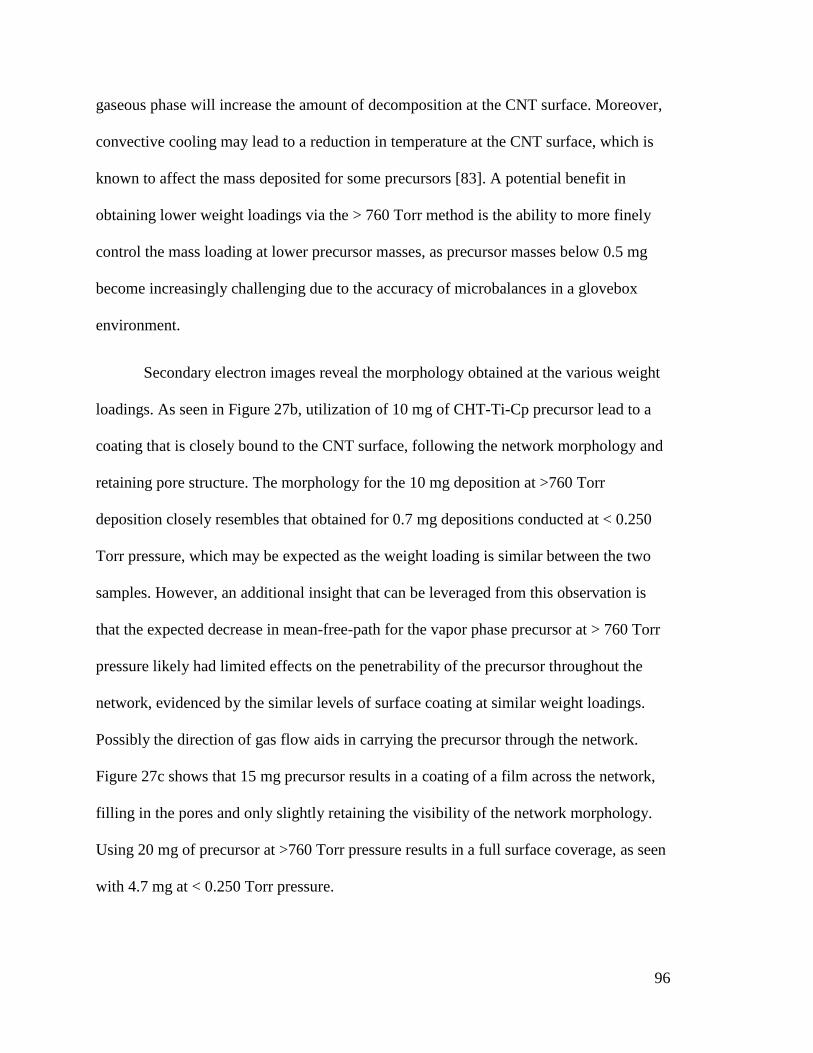
96
gaseous phase will increase the amount of decomposition at the CNT surface. Moreover,
convective cooling may lead to a reduction in temperature at the CNT surface, which is
known to affect the mass deposited for some precursors [83]. A potential benefit in
obtaining lower weight loadings via the > 760 Torr method is the ability to more finely
control the mass loading at lower precursor masses, as precursor masses below 0.5 mg
become increasingly challenging due to the accuracy of microbalances in a glovebox
environment.
Secondary electron images reveal the morphology obtained at the various weight
loadings. As seen in Figure 27b, utilization of 10 mg of CHT-Ti-Cp precursor lead to a
coating that is closely bound to the CNT surface, following the network morphology and
retaining pore structure. The morphology for the 10 mg deposition at >760 Torr
deposition closely resembles that obtained for 0.7 mg depositions conducted at < 0.250
Torr pressure, which may be expected as the weight loading is similar between the two
samples. However, an additional insight that can be leveraged from this observation is
that the expected decrease in mean-free-path for the vapor phase precursor at > 760 Torr
pressure likely had limited effects on the penetrability of the precursor throughout the
network, evidenced by the similar levels of surface coating at similar weight loadings.
Possibly the direction of gas flow aids in carrying the precursor through the network.
Figure 27c shows that 15 mg precursor results in a coating of a film across the network,
filling in the pores and only slightly retaining the visibility of the network morphology.
Using 20 mg of precursor at >760 Torr pressure results in a full surface coverage, as seen
with 4.7 mg at < 0.250 Torr pressure.
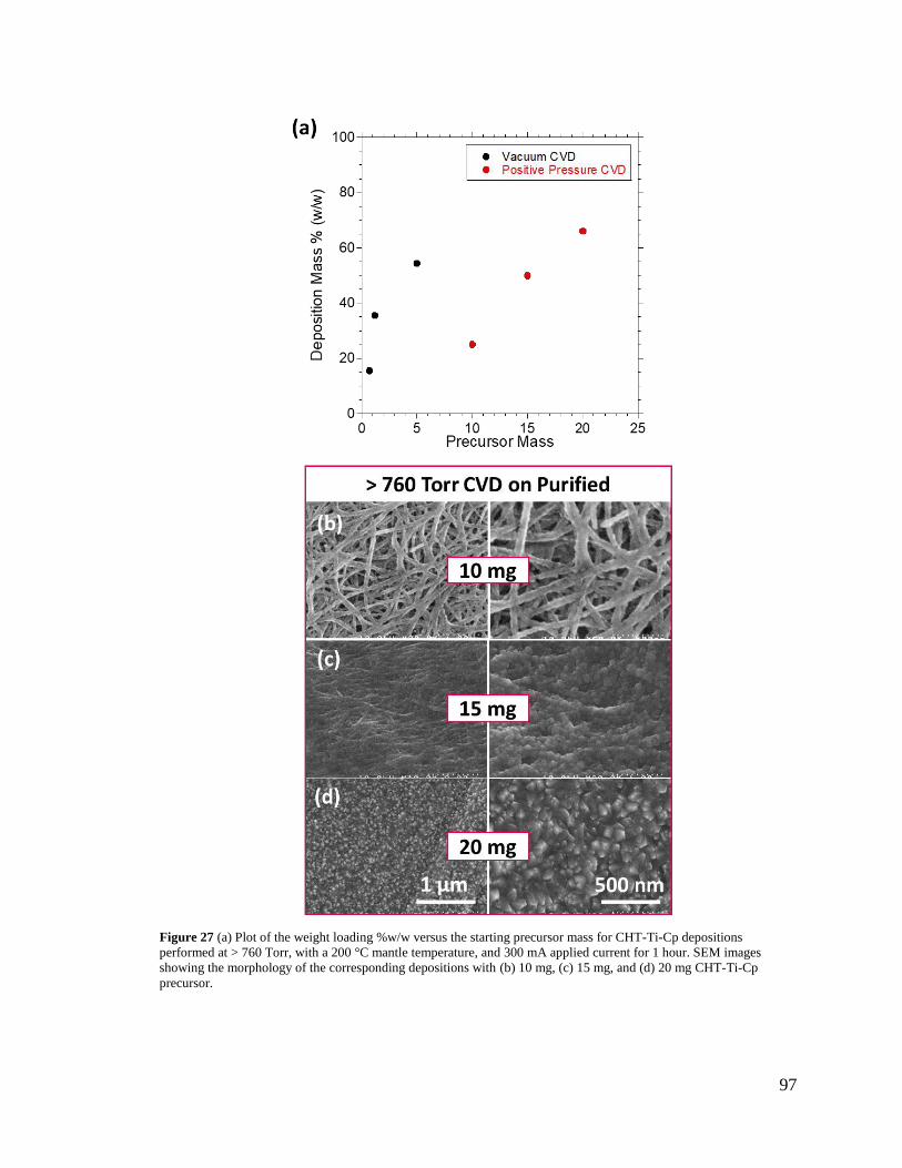
97
Figure 27 (a) Plot of the weight loading %w/w versus the starting precursor mass for CHT-Ti-Cp depositions
performed at > 760 Torr, with a 200 °C mantle temperature, and 300 mA applied current for 1 hour. SEM images
showing the morphology of the corresponding depositions with (b) 10 mg, (c) 15 mg, and (d) 20 mg CHT-Ti-Cp
precursor.
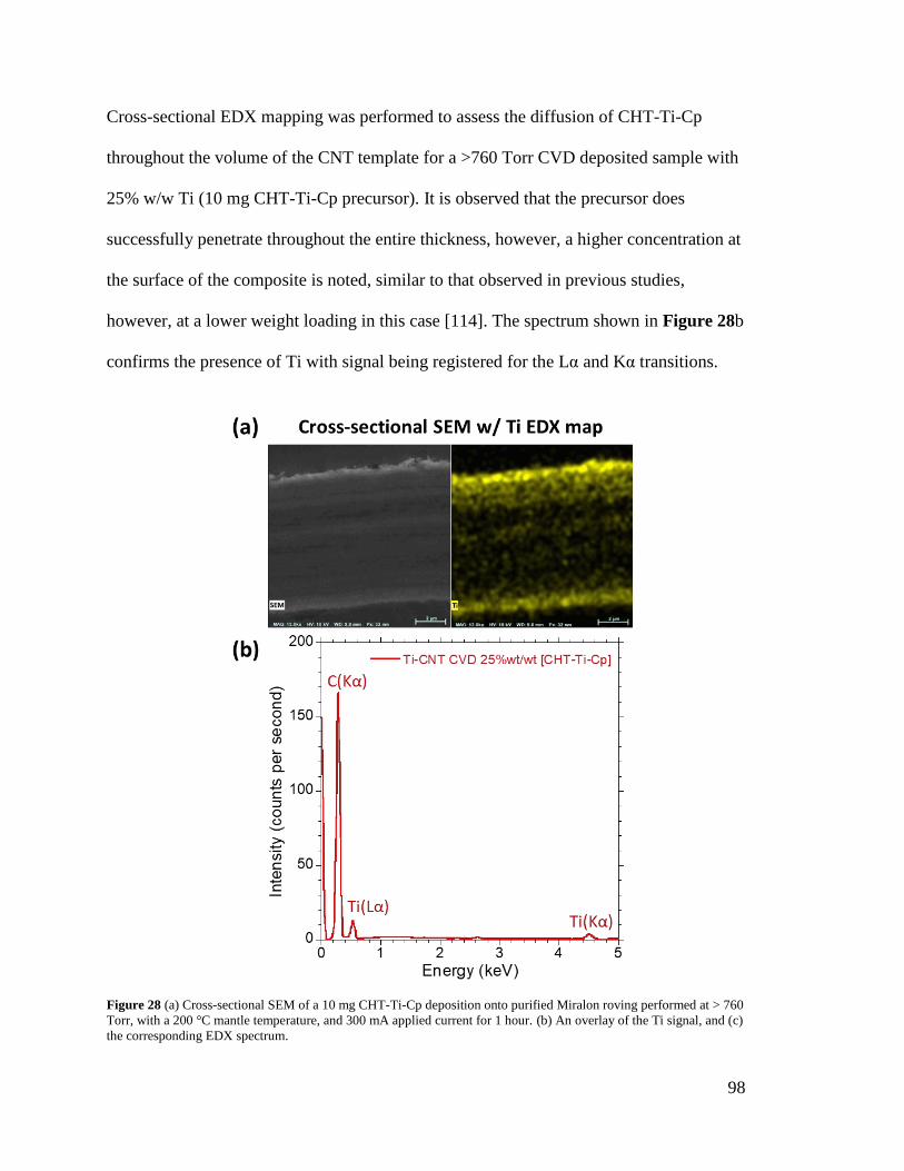
98
Cross-sectional EDX mapping was performed to assess the diffusion of CHT-Ti-Cp
throughout the volume of the CNT template for a >760 Torr CVD deposited sample with
25% w/w Ti (10 mg CHT-Ti-Cp precursor). It is observed that the precursor does
successfully penetrate throughout the entire thickness, however, a higher concentration at
the surface of the composite is noted, similar to that observed in previous studies,
however, at a lower weight loading in this case [114]. The spectrum shown in Figure 28b
confirms the presence of Ti with signal being registered for the Lα and Kα transitions.
Figure 28 (a) Cross-sectional SEM of a 10 mg CHT-Ti-Cp deposition onto purified Miralon roving performed at > 760
Torr, with a 200 °C mantle temperature, and 300 mA applied current for 1 hour. (b) An overlay of the Ti signal, and (c)
the corresponding EDX spectrum.

99
Raman spectroscopy showcases the standard graphitic peak and defect band
associated with CNTs as described earlier, however, a lack of any peak corresponding to
the vibrational modes for TiO2 are present (see Figure 29), in contrast with that observed
for the depositions performed at < 0.250 Torr. Environmental control is thus attributed as
being a major factor influencing oxidation during growth. The reduction in amount of
oxide present after CVD deposition demonstrates a path forward toward Ti-rich
depositions throughout a 3-D CNT network, providing a direct approach toward the
fabrication of fully interconnected Ti-CNT hybrids.
Figure 29 Raman spectroscopy measurements of a 10 mg CHT-Ti-Cp deposition onto purified Miralon CNT roving
performed at > 760 Torr, with a 200 °C mantle temperature, and 300 mA applied current for 1 hour.
5.2 Evaluation of Metal Grain Structure on Hybrid Electrical Properties
To understand the impact of metallization on the electrical interconnection
between CNT bundles, temperature-dependent electrical measurements were taken and

100
analyzed via electron transport modeling. A Janis VPF-800 cryostat was used to perform
the temperature-dependent electrical measurements under 10-6 mbar vacuum. Multiple
cycles of temperature sweeps from 80 – 600 K were performed with four-point probe I-V
sweeps being carried out at 5 °C increments, using a National Instruments NI PXI-4110
programmable power supply and NI PXI-4072 digital multimeter to acquire the electrical
measurements. Figure 30 shows a typical I-V sweep measurement for metallized CNT
hybrids, which is used to calculate resistance values. As shown previously, the first
temperature cycle can modify material properties either through annealing, or desorption
of weakly bound ambient species [99]. To ensure that analysis of the curves are
representative of the permanent material characteristics, multiple temperature cycles were
carried out until the temperature response during an up and down ramp remained stable
(i.e. no change in response regardless of ramp direction).
101
Figure 30 Individual I-V sweeps for a Ti-CNT sample fabricated using 10 mg CHT-Ti-Cp deposition onto purified
Miralon CNTs performed at > 760 Torr, with a 200 °C mantle temperature, and 300 mA applied current for 1 hour. The
I-V sweep in this figure represents a typical I-V response for the metallized CNT hybrids and is used to determine the
resistance values for temperature dependent electrical data.
Figure 31 shows temperature-dependent electrical data taken for Ti-CNT composites
fabricated with 0.7 and 5 mg CHT-Ti-Cp precursor at < 0.250 Torr pressure (16% and
54% w/w Ti respectively), as well as 10 mg CHT-Ti-Cp precursor deposited at > 760
Torr pressure (25% w/w Ti). Additionally, the samples prepared at < 0.250 Torr pressure
were subjected to a 6 hour, 400 °C (673.15 K) vacuum anneal within the Janis cryostat at
10-6 mbar pressure to assess the impact of annealing on the temperature dependent
properties. Conductivities were estimated based on average cross-sectional area of the
Miralon. Fitting of the curves was performed using the Kaiser model [16] described in
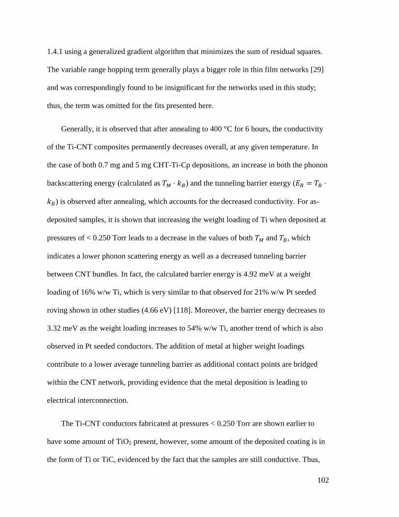
102
1.4.1 using a generalized gradient algorithm that minimizes the sum of residual squares.
The variable range hopping term generally plays a bigger role in thin film networks [29]
and was correspondingly found to be insignificant for the networks used in this study;
thus, the term was omitted for the fits presented here.
Generally, it is observed that after annealing to 400 °C for 6 hours, the conductivity
of the Ti-CNT composites permanently decreases overall, at any given temperature. In
the case of both 0.7 mg and 5 mg CHT-Ti-Cp depositions, an increase in both the phonon
backscattering energy (calculated as 𝑇𝑀 ⋅ 𝑘𝐵) and the tunneling barrier energy (𝐸𝐵 = 𝑇𝐵 ⋅
𝑘𝐵) is observed after annealing, which accounts for the decreased conductivity. For as-
deposited samples, it is shown that increasing the weight loading of Ti when deposited at
pressures of < 0.250 Torr leads to a decrease in the values of both 𝑇𝑀 and 𝑇𝐵, which
indicates a lower phonon scattering energy as well as a decreased tunneling barrier
between CNT bundles. In fact, the calculated barrier energy is 4.92 meV at a weight
loading of 16% w/w Ti, which is very similar to that observed for 21% w/w Pt seeded
roving shown in other studies (4.66 eV) [118]. Moreover, the barrier energy decreases to
3.32 meV as the weight loading increases to 54% w/w Ti, another trend of which is also
observed in Pt seeded conductors. The addition of metal at higher weight loadings
contribute to a lower average tunneling barrier as additional contact points are bridged
within the CNT network, providing evidence that the metal deposition is leading to
electrical interconnection.
The Ti-CNT conductors fabricated at pressures < 0.250 Torr are shown earlier to
have some amount of TiO2 present, however, some amount of the deposited coating is in
the form of Ti or TiC, evidenced by the fact that the samples are still conductive. Thus,
103
the Ti present is attributed to the low tunneling barrier obtained. Temperature-dependent
electrical measurements were also taken for a Ti-CNT conductor that was fabricated via
CVD at > 760 Torr pressure, to assess if the presence of TiO2 in the samples fabricated at
< 0.250 Torr influence the electrical interface. In this case, a Ti-CNT conductor with 25%
w/w Ti was modeled and exhibits a tunneling barrier energy of 2.40 meV, which is lower
than that obtained for samples fabricated at < 0.250 Torr pressure even with higher
weight loadings. Thus, minimizing the amount of TiO2 in the deposited coatings is
attributed to providing a lower barrier height between CNTs.
104
Figure 31 Temperature-dependent electrical measurements with curve fitting results for (a) 0.7 mg, and (b) 5 mg CHT-
Ti-Cp depositions onto purified Miralon CNTs performed at < 0.250 Torr, with a 200 °C mantle temperature, and 250
mA applied current for 1 hour. (c) 10 mg CHT-Ti-Cp deposition onto purified Miralon CNTs performed at > 760 Torr,
with a 200 °C mantle temperature, and 300 mA applied current for 1 hour.
105
5.3 Transferability of Process Principles to another Material System: W-
CNT Hybrids
The effectiveness of pure Ti as an adhesion metal on CNTs is benefitted from its
wettability, temperature stability, and low contact resistance to CNTs. W is an alternative
metal that exhibits similar properties to Ti with respect to CNTs, but also has a tendency
to form stable oxides. The processing principles developed for the Ti-CNT system are
evaluated in this section for a W-CNT composite to assess the effectiveness of the
process and establish the basis for an alternative metal-CNT system.
5.3.1 Vacuum CVD (< 0.250 Torr)
In this study, the purified Miralon roving described in section 5.1.1 is used as the
base CNT material, and the resulting material properties after CVD are assessed via a
combination of electron microscopy, energy dispersive X-ray spectroscopy, mass
measurements, and Raman spectroscopy.
A three-neck flask set-up is used for the deposition of W via Joule-heating driven
CVD as described in earlier works. A single strand of purified Miralon CNT roving is
suspended between two electrical leads passed through rubber septa enclosing the outer
two necks. The flask is brought into a glovebox purged under an argon environment. The
precursor was massed inside of the glovebox using a Mettler Toledo XP-2U
microbalance to measure masses as low as 3 mg. Bis(cyclopentadienyl) Tungsten(IV)
(CAS# 1271-33-6, Sigma-Aldrich 97%) [W(Cp)2H2] was used as the precursor in this
study. The massed precursor was transferred into the three-neck flask within the
glovebox and the flask was transferred into a hood equipped with a Schlenk line to
control the environment of the flask. The Schlenk line system consists of two lines; one
line for delivering 95% Ar/5% H2 gas, and the other for pulling vacuum on the system.
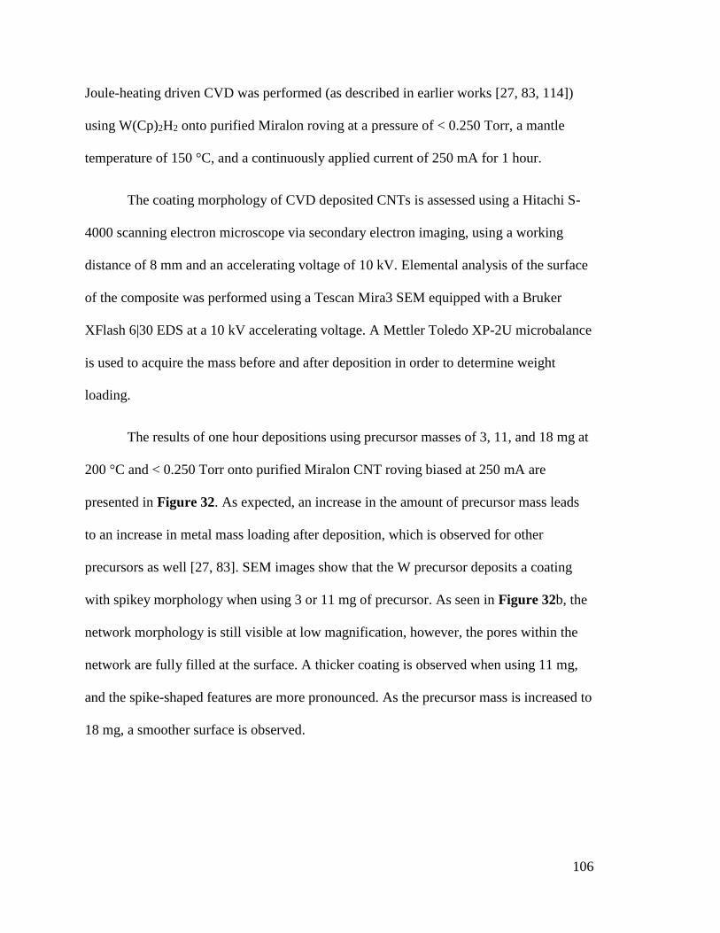
106
Joule-heating driven CVD was performed (as described in earlier works [27, 83, 114])
using W(Cp)2H2 onto purified Miralon roving at a pressure of < 0.250 Torr, a mantle
temperature of 150 °C, and a continuously applied current of 250 mA for 1 hour.
The coating morphology of CVD deposited CNTs is assessed using a Hitachi S-
4000 scanning electron microscope via secondary electron imaging, using a working
distance of 8 mm and an accelerating voltage of 10 kV. Elemental analysis of the surface
of the composite was performed using a Tescan Mira3 SEM equipped with a Bruker
XFlash 6|30 EDS at a 10 kV accelerating voltage. A Mettler Toledo XP-2U microbalance
is used to acquire the mass before and after deposition in order to determine weight
loading.
The results of one hour depositions using precursor masses of 3, 11, and 18 mg at
200 °C and < 0.250 Torr onto purified Miralon CNT roving biased at 250 mA are
presented in Figure 32. As expected, an increase in the amount of precursor mass leads
to an increase in metal mass loading after deposition, which is observed for other
precursors as well [27, 83]. SEM images show that the W precursor deposits a coating
with spikey morphology when using 3 or 11 mg of precursor. As seen in Figure 32b, the
network morphology is still visible at low magnification, however, the pores within the
network are fully filled at the surface. A thicker coating is observed when using 11 mg,
and the spike-shaped features are more pronounced. As the precursor mass is increased to
18 mg, a smoother surface is observed.

107
Figure 32 (a) Plot of the weight loading %w/w versus the starting precursor mass for W(Cp)2H2 depositions performed
at < 0.250 Torr, with a 150 °C mantle temperature, and 250 mA applied current for 1 hour. SEM images showing the
morphology of the corresponding depositions with (b) 3 mg, (c) 11 mg, and (d) 18 mg W(Cp)2H2 precursor.
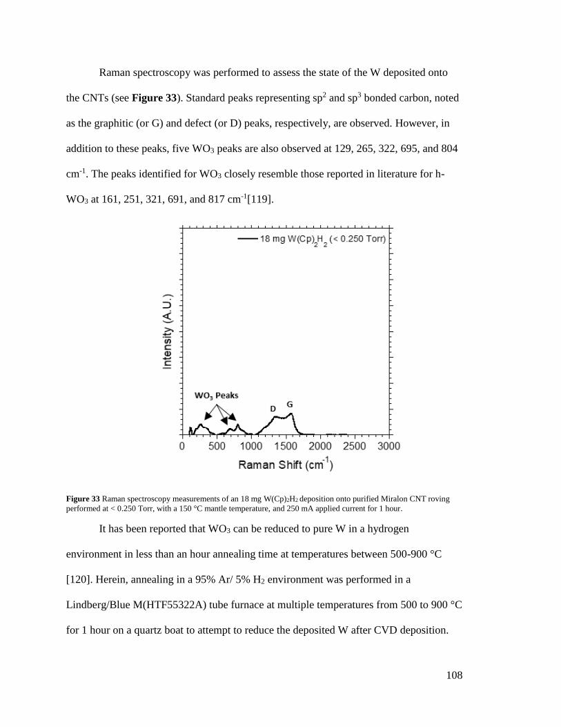
108
Raman spectroscopy was performed to assess the state of the W deposited onto
the CNTs (see Figure 33). Standard peaks representing sp2 and sp3 bonded carbon, noted
as the graphitic (or G) and defect (or D) peaks, respectively, are observed. However, in
addition to these peaks, five WO3 peaks are also observed at 129, 265, 322, 695, and 804
cm-1. The peaks identified for WO3 closely resemble those reported in literature for h-
WO3 at 161, 251, 321, 691, and 817 cm-1[119].
Figure 33 Raman spectroscopy measurements of an 18 mg W(Cp)2H2 deposition onto purified Miralon CNT roving
performed at < 0.250 Torr, with a 150 °C mantle temperature, and 250 mA applied current for 1 hour.
It has been reported that WO3 can be reduced to pure W in a hydrogen
environment in less than an hour annealing time at temperatures between 500-900 °C
[120]. Herein, annealing in a 95% Ar/ 5% H2 environment was performed in a
Lindberg/Blue M(HTF55322A) tube furnace at multiple temperatures from 500 to 900 °C
for 1 hour on a quartz boat to attempt to reduce the deposited W after CVD deposition.

109
Raman measurements on the annealed samples show that the peaks associated with WO3
remain after annealing to 500 and 600 °C, however, successful reduction is achieved at
900 °C, whereby all peaks related to oxides are vacant, and a pristine CNT curve is
observed from beneath the surface (see Figure 34). Moreover, a significant recovery of
the D/G ratio is observed, indicating that the high temperature annealing didn’t
negatively impact the CNT structure.
Figure 34 Raman spectroscopy measurements of an 18 mg W(Cp)2H2 deposition onto purified Miralon CNT roving
performed at < 0.250 Torr, with a 150 °C mantle temperature, and 250 mA applied current for 1 hour after annealing to
500, 600, and 900 °C in a 95% Ar/ 5% H2 environment.
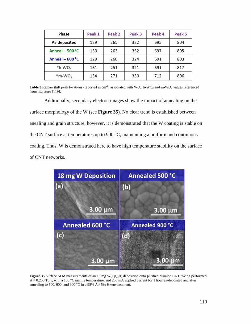
110
Table 3 Raman shift peak locations (reported in cm-1) associated with WO3. h-WO3 and m-WO3 values referenced
from literature [119].
Additionally, secondary electron images show the impact of annealing on the
surface morphology of the W (see Figure 35). No clear trend is established between
anealing and grain structure, however, it is demonstrated that the W coating is stable on
the CNT surface at temperatures up to 900 °C, maintaining a uniform and continuous
coating. Thus, W is demonstrated here to have high temperature stability on the surface
of CNT networks.
Figure 35 Surface SEM measurements of an 18 mg W(Cp)2H2 deposition onto purified Miralon CNT roving performed
at < 0.250 Torr, with a 150 °C mantle temperature, and 250 mA applied current for 1 hour as-deposited and after
annealing to 500, 600, and 900 °C in a 95% Ar/ 5% H2 environment.

111
5.3.2 >760 Torr CVD
Annealing in a reducing atmosphere successfully converted the CVD deposited WO3 film
to pure W. Joule-heating CVD at > 760 Torr pressure is explored as an alternative route
to achieve W-rich films by encouraging a pure W deposition onto the CNTs during
growth. In this study, the modified three-neck flask set-up was used to accommodate
pressures greater than 760 Torr, with a continuous flow of 95% Ar / 5% H2 (mol/mol) gas
as shown in Figure 26. CVD experiments presented here are conducted with an applied
current of 300 mA for 1 hour, using a mantle temperature of 150 °C to sublimate a
W(Cp)2H2 precursor.
The influence of precursor mass on the resultant deposition mass loading and
morphology are presented in Figure 36a, using 5, 10, and 21 mg of precursor. As
observed in the case for CHT-Ti-Cp deposition at > 760 Torr, the weight loading after
deposition increases correspondingly with increasing precursor mass. Furthermore, it is
again observed here that for a given precursor mass, the resultant weight loading after
deposition at > 760 Torr pressure was lower when compared to < 0.250 Torr depositions,
which is attributed to the lower mass fraction of vapor phase precursor as described
earlier as well as potential convective cooling effects.
Secondary electron images showcase the morphology obtained at the various
weight loadings. As seen in Figure 36b, utilization of 5 mg of CHT-Ti-Cp precursor led
to a continuous and uniform coating that adheres closely to the to the CNT network
morphology. Notably, the surface texture is much more smooth in comparison to the
spike-shaped features obtained via < 0.250 Torr depositions of W(Cp)2H2. The
morphology for the 10 mg and 21 mg depositions performed at >760 Torr deposition

112
show greater amount of filling due to the higher weight loading. Importantly, depositions
at all weight loadings showcase a smoother surface texture without the presence of spike-
shaped features that were observed in the < 0.250 Torr depositions, which may be
resultant of oxide formation.
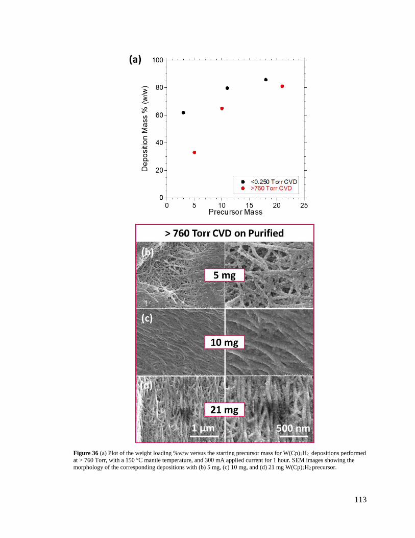
113
Figure 36 (a) Plot of the weight loading %w/w versus the starting precursor mass for W(Cp)2H2 depositions performed
at > 760 Torr, with a 150 °C mantle temperature, and 300 mA applied current for 1 hour. SEM images showing the
morphology of the corresponding depositions with (b) 5 mg, (c) 10 mg, and (d) 21 mg W(Cp)2H2 precursor.

114
To verify the deposition of W onto the CNTs, surface-view EDS mapping was
performed on a W-CNT sample with a weight loading of 65% w/w, shown in Figure 37.
Uniform coverage of W is shown across the surface of the CNTs, with a strong W signal
confirming the presence of W. The confirmation of W deposition validates W(Cp)2H2 as
a viable precursor for CVD depositions of W onto CNT networks.
Figure 37 (a) Surface-view SEM of a 10 mg W(Cp)2H2 deposition on purified Miralon CNTs performed at > 760 Torr,
with a 150 °C mantle temperature, and 300 mA applied current for 1 hour. EDX map overlay of W signal in bottom
image. (b) Corresponding EDX spectrum.
Raman spectroscopy was performed to understand the phase of W deposited onto
the CNTs, shown in Figure 38. Standard G, D, and G’ peaks are observed for the W-
CNT composite, which correspond to the vibrational modes observed in CNTs. No peaks
are observed that would correspond to WO3, however, which is consistent with that
observed for >760 Torr CVD depositions performed with CHT-Ti-Cp, whereby oxide
formation was minimized. Moreover, a small amount of signal is registered at 690 and
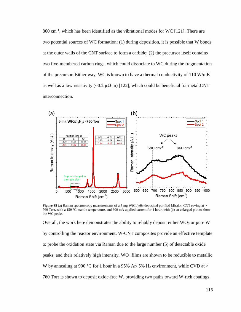
115
860 cm-1, which has been identified as the vibrational modes for WC [121]. There are
two potential sources of WC formation: (1) during deposition, it is possible that W bonds
at the outer walls of the CNT surface to form a carbide; (2) the precursor itself contains
two five-membered carbon rings, which could dissociate to WC during the fragmentation
of the precursor. Either way, WC is known to have a thermal conductivity of 110 W/mK
as well as a low resistivity (~0.2 µΩ·m) [122], which could be beneficial for metal:CNT
interconnection.
Figure 38 (a) Raman spectroscopy measurements of a 5 mg W(Cp)2H2 deposited purified Miralon CNT roving at >
760 Torr, with a 150 °C mantle temperature, and 300 mA applied current for 1 hour, with (b) an enlarged plot to show
the WC peaks.
Overall, the work here demonstrates the ability to reliably deposit either WO3 or pure W
by controlling the reactor environment. W-CNT composites provide an effective template
to probe the oxidation state via Raman due to the large number (5) of detectable oxide
peaks, and their relatively high intensity. WO3 films are shown to be reducible to metallic
W by annealing at 900 °C for 1 hour in a 95% Ar/ 5% H2 environment, while CVD at >
760 Torr is shown to deposit oxide-free W, providing two paths toward W-rich coatings
116
on the CNT surface. Additionally, the lack of tungsten oxide formation during CVD
deposition at > 760 Torr pressure with the W(Cp)2H2 precursor corroborates the
observation of oxide-free Ti deposition shown earlier using the CHT-Ti-Cp precursor,
further cementing the ability to deposit Ti-rich or W-rich films.
5.4 Outcomes
The work presented in this chapter has provided an understanding of the influence that
reactor environment and pressure have on the deposition properties. Success of oxide-free
deposition was achieved using a pressure > 760 Torr in an inert/reducing environment,
attributed to the absence of any leaks. However, modifying the pressure also influences
other aspects of the deposition dynamics. Namely, at pressures > 760 Torr, lower weight
loadings are deposited for a given precursor mass, and thus, finer control over low weight
loadings is possible. Additionally, depositions at > 760 Torr offer a route towards CVD
onto CNT samples that are sensitive to vacuum environments. At the same time, for
applications where higher weight loadings are desirable, deposition at < 0.250 Torr
benefits from achieving higher weight loadings while using less precursor. Moreover, a
vacuum environment enables longer mean-free-paths for vapor-phase precursors, which
may affect diffusion dynamics during deposition. For follow-on studies, an alternative
set-up could be implemented in which the reactor flask is situated within an
environmental enclosure. In this manner, the flask could be held under vacuum, while the
surrounding environment is purged with argon, such that any potential leaks into the flask
would be inert. Such a set-up would allow for the study of the pressure effects on the
reaction dynamics more closely.
117
6 Dissertation Conclusions and Impact The dissertation focused on the nature of adhesion metal interactions with carbon
nanotubes. In particular, Ti, Ni, and W were explored as candidate metals due to their
wettability, ability to form carbides, and their low contact resistance to CNTs. Multiple
deposition techniques were evaluated to create both 2-D thin film structures as well as the
use of a novel CVD approach for 3-D deposition. Sample processing methods such as
annealing and temperature-cycling were explored to understand the stability of the metals
at elevated temperature. The sample test structures were interrogated by SEM, Raman
spectroscopy, etc. to explore the morphology and structure that was produced. Electrical
measurements and mass characterization provided detailed relationships between
experimental conditions and the resulting physical properties. Each of these experiments
were directed at understanding the fundamental interaction and susceptibility to
electroplated coatings for enhanced hybrid conductors. Ultimately, the experimental
work was complemented by a physics-based model to extract parameters that can aid in
understanding the conduction mechanism for novel hybrids. The outcomes of each
chapter section are provided below as well as summary for the dissertation impacts along
with pathways for future work.
Chapter 3 utilizes thermal evaporation to directly evaluate the interfacial
characteristics of a 2-D Ti film on a CNT ribbon conductor. Specifically, a 10 nm layer of
Ti was shown via secondary electron imaging to deposit continuously and uniformly
along the CNT network, indicative of a high binding energy to the CNTs as-deposited.
The 10 nm Ti layer was demonstrated to maintain a tightly adhered coating up to 400 °C
for 1 hour in 95% Ar / 5% H2, warranting its use as an adhesion metal for elevated

118
temperature applications. A 100 nm Cu layer was deposited onto the as-received CNT
conductor and annealed to 400 °C, resulting in gap formation throughout the film as the
Cu began to delaminate from the surface due to poor interaction. Additionally, as a result
of film delamination, the annealed Cu-Ti-CNT hybrid increased in resistance by 40%.
Utilizing a 10 nm Ti layer in a Cu-Ti-CNT hybrid succesfully suppressed delamination of
the Cu overcoat, and achieved a 12% reduction in the resistance per length,
demonstrating the advantages of Ti as an adhesion metal for elevated temperature
applications.
Chapter 4 demonstrates the ability to deposit Ti throughout the entire volume of a
porous 3-D CNT conductor via Joule-heating driven CVD using a CHT-Ti-Cp precursor.
The diffusion of Ti throughout the ~30 µm thickness was verified through cross-sectional
EDS mapping, showing for the first time the fabrication of integrated bulk Ti-CNT
conductors via this technique. Moreover, control over coating morphology and weight
loading is demonstrated by varying precursor mass, achieving coatings tightly bound to
the CNT network geometry as well as fully connected thin films on the bulk conductor
surface. Additionally, electroplating was employed to fabricate Cu-Ti-CNT hybrids,
achieving conductivities as high as 43.1 MS/m after densification and annealing, which is
the highest value reported in literature for bulk metal-CNT conductors at 98% or lower
metal mass loading. Favorable interaction between the metals and the CNTs resulted in a
TCR of 3.49 × 10⁻³ K-1, combined with a specific conductivity of 6257 Sm2/kg, which
results in a conductor that surpasses the specific conductivity of pure Cu at or above a
temperature of 250 °C. This work demonstrates the fabrication of advanced metal-CNT
119
hybrids that can provide direct energy savings during operation at elevated temperatures
for applications such as high efficiency motors.
Chapter 5 establishes CVD reactor environment controls that enable either mixed
Ti-oxide or oxide-free depositions, performing depositions at < 0.250 Torr or > 760 Torr
in a 95% Ar/ 5% H2 envinronment. Depositions performed at > 760 Torr are shown to
have lower resultant weight loadings for a given starting precursor mass when compared
to depositions performed at < 0.250 Torr, allowing for higher precision of control when
targeting low masses. Additionally, Raman spectroscopy measurements indicate a lack of
oxide formation during depositions at > 760 Torr. The control over oxide formation was
verified by depositing W onto CNTs at < 0.250 Torr and > 760 Torr, corroborating the
same trends observed for Ti depositions. The W-CNT acts a useful template for probing
oxide formation due to WO3 having 5 easily detectable peaks measurable by Raman.
Moreover, in depositions performed at > 760 Torr pressure, the presence of WC was
observed, indicating an oxygen-free reaction environment. The results here demonstrate a
path toward W-rich and Ti-rich throughout a 3-D porous CNT conductor.
Additionally, in Chapter 5, the impact of oxide formation as well as weight
loading on the electrical properties of the Ti-CNT conductors is evaluated via modeling
of the temperature-dependent conductivity. Curve fitting revealed that the tunneling
barrier between CNT bundles within the network decreased with increased weight
loading of Ti deposited at < 0.250 Torr pressure. Furthermore, Ti deposited at > 760 Torr
was determined to have an even lower tunneling barrier than depositions performed at <
0.250 Torr, even with higher weight loadings, attributed to the reduced amount of oxides
present within the metal coating. The modeling performed herein directly supports the
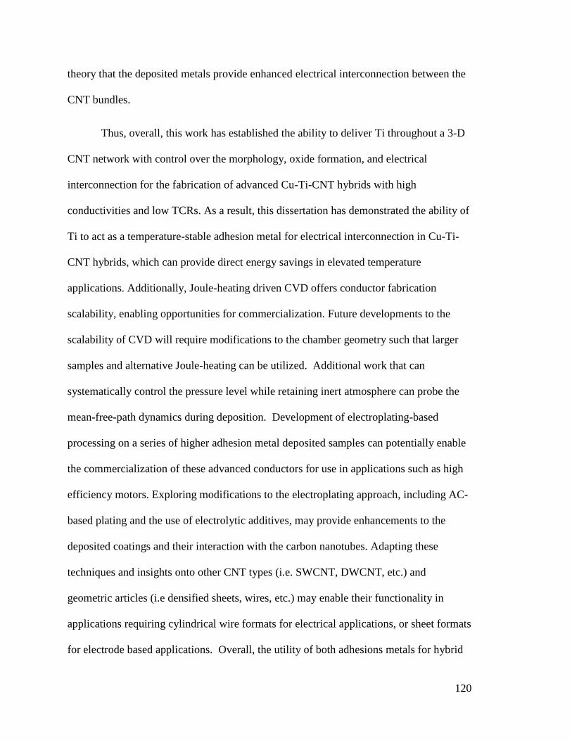
120
theory that the deposited metals provide enhanced electrical interconnection between the
CNT bundles.
Thus, overall, this work has established the ability to deliver Ti throughout a 3-D
CNT network with control over the morphology, oxide formation, and electrical
interconnection for the fabrication of advanced Cu-Ti-CNT hybrids with high
conductivities and low TCRs. As a result, this dissertation has demonstrated the ability of
Ti to act as a temperature-stable adhesion metal for electrical interconnection in Cu-Ti-
CNT hybrids, which can provide direct energy savings in elevated temperature
applications. Additionally, Joule-heating driven CVD offers conductor fabrication
scalability, enabling opportunities for commercialization. Future developments to the
scalability of CVD will require modifications to the chamber geometry such that larger
samples and alternative Joule-heating can be utilized. Additional work that can
systematically control the pressure level while retaining inert atmosphere can probe the
mean-free-path dynamics during deposition. Development of electroplating-based
processing on a series of higher adhesion metal deposited samples can potentially enable
the commercialization of these advanced conductors for use in applications such as high
efficiency motors. Exploring modifications to the electroplating approach, including AC-
based plating and the use of electrolytic additives, may provide enhancements to the
deposited coatings and their interaction with the carbon nanotubes. Adapting these
techniques and insights onto other CNT types (i.e. SWCNT, DWCNT, etc.) and
geometric articles (i.e densified sheets, wires, etc.) may enable their functionality in
applications requiring cylindrical wire formats for electrical applications, or sheet formats
for electrode based applications. Overall, the utility of both adhesions metals for hybrid

121
CNT conductors and the benefits of using joule-heating CVD to realize the depositions
show tremendous promise in this emerging field of metal-CNT conductors.

122
7 Appendix A: Additional Experiments Data sets included here are based on screening experiments to better understand CVD
parameters. The experiments performed here were sufficiently rigorous to be valid, but
don’t fit into a complete story, and are intended to explore alternative experimental
pathways.
7.1 Serial Deposition towards Ti Passivation
A potential source of oxidation for Ti coatings on CNTs can come from
environmental exposure. Encapsulation of the Ti layer can prevent the formation of
native oxides by eliminating exposure to the environment. Serial CVD deposition is
suggested to coat a Ti layer with a Cu overcoat prior to exposure to the ambient
environment. In this way, a CVD deposition of 7.5 mg CHT-Ti-Cp was performed at <
0.250 Torr with a mantle temperature of 200 °C and applied current of 350 mA for one
hour. Immediately after the Ti deposition was performed, the flask was transferred into a
glovebox, where 13 mg of Cu(acac)2 precursor was loaded into the flask. The flask was
then transferred back to the Schlenk line and a subsequent CVD deposition was
performed at the same conditions. Figure 39 shows the surface morphology of the Ti-
CNT and Cu-Ti-CNT depositions. A spike-shaped morphology is observed the Ti, which
is shown to be stable after an anneal to 300 °C in 95% Ar / 5% H2. The Cu deposition
appears to have some degree of coating on the spike-shaped features, with additional
spherical particles throughout. After annealing, the spherical Cu particles grow in size,
however, the coating underneath the spheres remains intact as well, suggesting that the Ti
layer may be helping with the adhesion of the Cu. More studies are needed to encourage
a continuous Cu coating along the surface, potentially by focusing on improving the Ti
adhesion layer through oxide-free deposition controls.
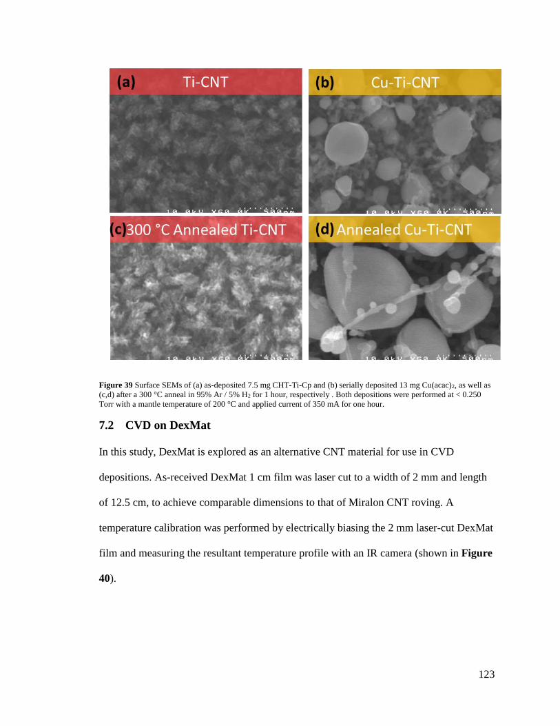
123
Figure 39 Surface SEMs of (a) as-deposited 7.5 mg CHT-Ti-Cp and (b) serially deposited 13 mg Cu(acac)2, as well as
(c,d) after a 300 °C anneal in 95% Ar / 5% H2 for 1 hour, respectively . Both depositions were performed at < 0.250
Torr with a mantle temperature of 200 °C and applied current of 350 mA for one hour.
7.2 CVD on DexMat
In this study, DexMat is explored as an alternative CNT material for use in CVD
depositions. As-received DexMat 1 cm film was laser cut to a width of 2 mm and length
of 12.5 cm, to achieve comparable dimensions to that of Miralon CNT roving. A
temperature calibration was performed by electrically biasing the 2 mm laser-cut DexMat
film and measuring the resultant temperature profile with an IR camera (shown in Figure
40).

124
Figure 40 (a) IR images of the 2 mm wide laser cut DexMat film biased at currents ranging from 0.2 to 1.4 A, as well
as (b) the corresponding average and maximum temperature of the conductor at each applied current.
Joule-heating driven CVD was performed on the 2 mm laser-cut DexMat film using 21.3
mg CHT-Ti-Cp precursor with a constant flow of 95% Ar/ 5% H2 (>760 Torr), a mantle
temperature of 200 °C, and electrical bias of 1.3 A for 1 hour, resulting a deposition of
36% w/w Ti. Figure 41 shows the surface morphology of the Ti, showcasing the
successful deposition of a fully connected film on the surface.
It is worth noting here that, despite having similar dimensions to the Miralon
roving, and depositing with matched conditions, CHT-Ti-Cp CVD performed on DexMat
achieved a weight loading of only 36% compared to the 66% obtained on Miralon.
Several factors influence the amount of deposition that occurs during a run. It has been
shown in this dissertation that the amount of starting precursor mass directly affects the
resultant weight loading after CVD. Furthermore, decreasing reactor pressure results in
higher weight loading depositions as well, attributed to the fact that powdered precursor
more readily sublimes at lower pressures. Similarly, previous studies have shown that
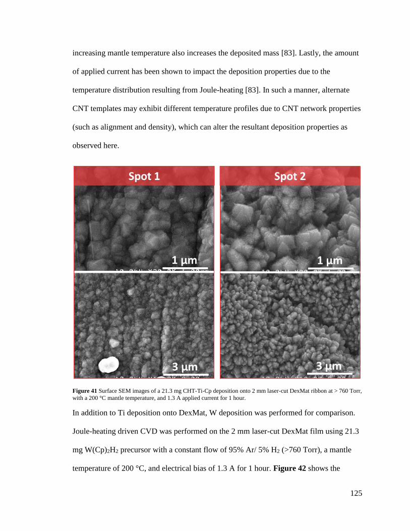
125
increasing mantle temperature also increases the deposited mass [83]. Lastly, the amount
of applied current has been shown to impact the deposition properties due to the
temperature distribution resulting from Joule-heating [83]. In such a manner, alternate
CNT templates may exhibit different temperature profiles due to CNT network properties
(such as alignment and density), which can alter the resultant deposition properties as
observed here.
Figure 41 Surface SEM images of a 21.3 mg CHT-Ti-Cp deposition onto 2 mm laser-cut DexMat ribbon at > 760 Torr,
with a 200 °C mantle temperature, and 1.3 A applied current for 1 hour.
In addition to Ti deposition onto DexMat, W deposition was performed for comparison.
Joule-heating driven CVD was performed on the 2 mm laser-cut DexMat film using 21.3
mg W(Cp)2H2 precursor with a constant flow of 95% Ar/ 5% H2 (>760 Torr), a mantle
temperature of 200 °C, and electrical bias of 1.3 A for 1 hour. Figure 42 shows the

126
surface morphology of the W, whereby a very light coating is observed, following along
the network morphology.
Figure 42 Surface SEM images of a 21.3 mg W(Cp)2H2 deposition onto 2 mm laser-cut DexMat ribbon at > 760 Torr,
with a 150 °C mantle temperature, and 1.3 A applied current for 1 hour.
Surface EDS mapping confirms the presence of W, with a uniform distribution across the
surface (Figure 43). Additionally, Fe and S are found in the sample, which likely result
from the catalyst used to synthesize the CNTs, and the acids used to process the CNT
product (such as chlorosulphonic acid, which contains S).
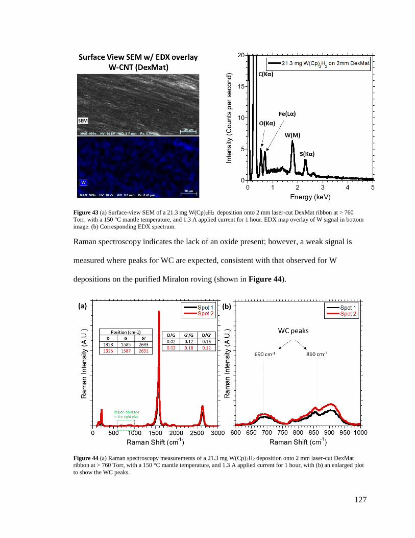
127
Figure 43 (a) Surface-view SEM of a 21.3 mg W(Cp)2H2 deposition onto 2 mm laser-cut DexMat ribbon at > 760
Torr, with a 150 °C mantle temperature, and 1.3 A applied current for 1 hour. EDX map overlay of W signal in bottom
image. (b) Corresponding EDX spectrum.
Raman spectroscopy indicates the lack of an oxide present; however, a weak signal is
measured where peaks for WC are expected, consistent with that observed for W
depositions on the purified Miralon roving (shown in Figure 44).
Figure 44 (a) Raman spectroscopy measurements of a 21.3 mg W(Cp)2H2 deposition onto 2 mm laser-cut DexMat
ribbon at > 760 Torr, with a 150 °C mantle temperature, and 1.3 A applied current for 1 hour, with (b) an enlarged plot
to show the WC peaks.
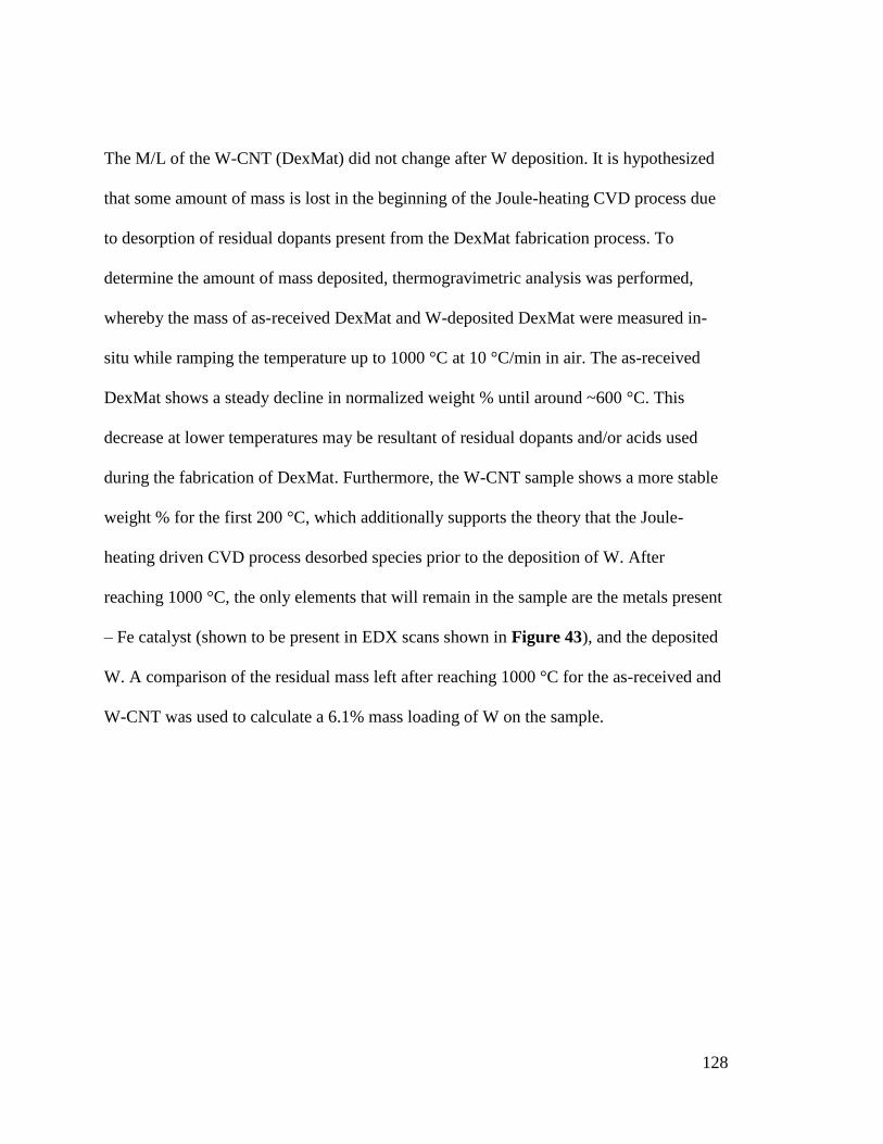
128
The M/L of the W-CNT (DexMat) did not change after W deposition. It is hypothesized
that some amount of mass is lost in the beginning of the Joule-heating CVD process due
to desorption of residual dopants present from the DexMat fabrication process. To
determine the amount of mass deposited, thermogravimetric analysis was performed,
whereby the mass of as-received DexMat and W-deposited DexMat were measured in-
situ while ramping the temperature up to 1000 °C at 10 °C/min in air. The as-received
DexMat shows a steady decline in normalized weight % until around ~600 °C. This
decrease at lower temperatures may be resultant of residual dopants and/or acids used
during the fabrication of DexMat. Furthermore, the W-CNT sample shows a more stable
weight % for the first 200 °C, which additionally supports the theory that the Joule-
heating driven CVD process desorbed species prior to the deposition of W. After
reaching 1000 °C, the only elements that will remain in the sample are the metals present
– Fe catalyst (shown to be present in EDX scans shown in Figure 43), and the deposited
W. A comparison of the residual mass left after reaching 1000 °C for the as-received and
W-CNT was used to calculate a 6.1% mass loading of W on the sample.

129
Figure 45 Thermogravimetric analysis measurements of as-received DexMat and a 21.3 mg W(Cp)2H2 deposition onto
2 mm laser-cut DexMat ribbon at > 760 Torr, with a 150 °C mantle temperature, and 1.3 A applied current for 1 hour.
7.3 IR Measurements of Various CNT Templates
Thermal imaging with an IR camera was performed on a variety of CNT templates under
electrical bias to generate an understanding of the temperature dynamics for use in CVD
or other applications. The CNT templates evaluated here consist of the following:
(1) Purified Miralon CNT roving subjected to a thermal oxidation up to 560 °C at 10
°C/min ramp, followed by an HCl rinse for 30 minutes, and an additional thermal
oxidation with the same conditions
(2) An experimental 40 tex Miralon roving
(3) The 40 tex Miralon roving with ultrasonically welded Cu pads for improved
current distribution over the wide injection area
(4) As-received DexMat 1 cm film
(5) As-received DexMat 1 cm film with ultrasonically welded Cu pads for current
distribution
0
20
40
60
80
100
120
0 200 400 600 800 1000
W-CNT CVD DexMat [W(Cp)2H
2]
DexMat As-Received
We
igh
t %
Temperature (°C)

130
(6) Laser-synthesized SWCNT ribbon cut from a purified paper.
The average temperature measured for a given applied current for each sample is shown
in Figure 46. In general, it is shown that the wider samples generate less heat at a given
current, which results from the lower resistance. Additionally, it is found that for the
widest samples (DexMat 1 cm film and 40 tex roving), hot spots accrue at the electrical
contact points. Ultrasonically welding Cu pads onto these samples results in a cooler
contact region, and improves the uniformity of the temperature profile overall. Thus, it is
shown here that it is crucial to use Cu pads on wider samples for proper current
distribution and improved heating uniformity.
Figure 46 (a) IR images of various CNT templates biased at currents at a range of currents up to 4 A, as well as (b) the
corresponding average temperature of the conductors at each applied current.
7.4 Alternative Ti Precursors
7.4.1 Dimethylbis(t-butylcyclopentadienyl) Titanium (IV) [tCp2-Ti-Me2]
Dimethylbis(t-butylcyclopentadienyl) Titanium (IV) [tCp2-Ti-Me2] was selected as an
alternative precursor to evaluate the performance of Ti on the CNT roving seeded via

131
CFH-CVD. The CVD process was conducted under static 0.300 Torr vacuum, with three
roving in parallel biased at 350 mA/roving for 1 hour. The mantle temperature was held
at 200 °C. A precursor mass of 6.5 mg lead to a weight loading of 25.1% w/w. As
observed in Figure 47, 6.5 mg of tCp2-Ti-Me2 precursor was sufficient to coat the CNTs
with a thin film while maintaining some of the network morphology. Finishing of the 6.5
mg tCp2-Ti-Me2 seeded conductor was performed by electroplating in a sandwich cell
configuration in Transene Cu acid solution at a current of 10 mA, followed by
densification and annealing at 300 °C for 3 hours in a reducing environment. The finished
6.5 mg tCp2-Ti-Me2 seeded conductor (97.4% Cu / 0.7% Ti / 1.9% CNT) exhibited a
specific conductivity of 3874 S·m2/kg, and conductivity of 36 MS/m, based on cross-
sectional SEM (see Figure 47b). Thus, tCp2-Ti-Me2 is shown here to be a viable
precursor for fabrication of high conductivity Cu-Ti-CNT hybrids.
Figure 47: a.) Surface SEM images of the 6.5 mg tCp2-Ti-Me2 seeded CNT roving. b.) False-colored cross-sectional
SEM of 6.5 mg tCp2-Ti-Me2 seeded CNT conductor electroplated at 10 mA current and finished.

132
7.4.2 Titanium Tetraisopropoxide (TTIP)
Cyclopentadienyl (Cycloheptatrienyl) Titanium (II) [CHT-Ti-Cp] and Titanium
Tetraisopropoxide (TTIP) precursors were selected to evaluate the deposition of Ti
compounds onto the CNT roving via CFH-CVD. The CVD process was conducted under
static 0.300 Torr vacuum, with three roving in parallel biased at 350 mA/roving for 1
hour. The mantle temperature was held at 200 °C for the CHT-Ti-Cp powder precursor,
however, the mantle was kept at 23 °C for the liquid TTIP precursor, as the vacuum alone
provides necessary conditions to evaporate the TTIP precursor. Deposition of 25 mg of
the TTIP and CHT-Ti-Cp precursor onto the CNT roving can be seen in Figure 48,
whereby the TTIP led to an 87.98% weight loading by mass, and the CHT-Ti-Cp led to a
67.15% weight loading. TTIP deposition is shown to form nano-needles, whereas the
CHT-Ti-Cp precursor deposits more bulbous structures. The R/L remained relatively
unchanged in the case of the CHT-Ti-Cp seeded conductor (354 ± 30 Ω/m), while the
TTIP precursor, which is known to form titanium oxides, deposited an insulating layer on
the surface of the roving.

133
Figure 48 Surface morphology of the TTIP and CHT-Ti-Cp depositions on CNT roving as taken by SEM.
To understand the phase of the titanium deposited onto the CNTs by the TTIP precursor,
Raman spectroscopy was performed. As see in Figure 49a, the TTIP seeded conductor
exhibits well-defined anatase TiO2 peaks, as compared to literature values.
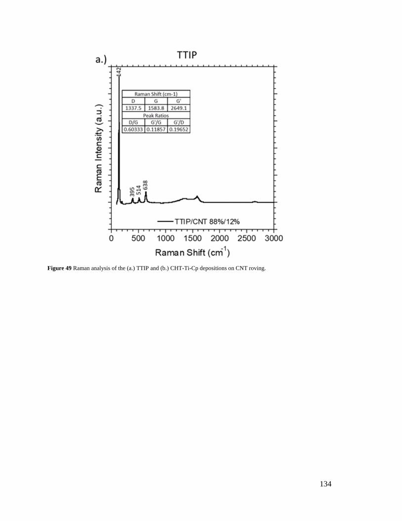
134
Figure 49 Raman analysis of the (a.) TTIP and (b.) CHT-Ti-Cp depositions on CNT roving.
135
8 Works Cited
1. Reich S, Thomsen C, Ordejón P (2002) Electronic band structure of isolated and
bundled carbon nanotubes. Phys Rev B - Condens Matter Mater Phys 65:1554111–
15541111. https://doi.org/10.1103/PhysRevB.65.155411
2. Landi BJ, Raffaelle RP (2007) Effects of carrier gas dynamics on single wall
carbon nanotube chiral distributions during laser vaporization synthesis. J Nanosci
Nanotechnol 7:883–890. https://doi.org/10.1166/jnn.2007.207
3. Jorio A, Saito R, Hertel T, et al (2018) C arbon Nanotube Photophysics
4. Cheng HM, Li F, Sun X, et al (1998) Bulk morphology and diameter distribution
of single-walled carbon nanotubes synthesized by catalytic decomposition of
hydrocarbons. Chem Phys Lett 289:602–610. https://doi.org/10.1016/S0009-
2614(98)00479-5
5. Wu AS, Chou TW, Gillespie JW, et al (2012) Electromechanical response and
failure behaviour of aerogel-spun carbon nanotube fibres under tensile loading. J
Mater Chem 22:6792–6798. https://doi.org/10.1039/c2jm15869h
6. Jarosz P, Schauerman C, Alvarenga J, et al (2011) Carbon nanotube wires and
cables: Near-term applications and future perspectives. Nanoscale 3:4542–4553.
https://doi.org/10.1039/c1nr10814j
7. Cress CD, Ganter MJ, Schauerman CM, et al (2017) Carbon nanotube wires with
continuous current rating exceeding 20 Amperes. J Appl Phys 122:.
https://doi.org/10.1063/1.4990981
136
8. Thomsen C, Maultzsch J (2004) Carbon Nanotubes: Basic Concepts and Physical
Properties. Wiley
9. Tans SJ, Devoret MH, Dai H, et al (1997) Individual single-wall carbon nanotubes
as quantum wires. Nature 386:474–477
10. White CT, Todorov TN (1998) Carbon nanotubes as long ballistic conductors.
Nature 393:240–241. https://doi.org/10.1038/30420
11. Zhang Z, Peng J, Zhang H (2001) Low-temperature resistance of individual single-
walled carbon nanotubes: A theoretical estimation. Appl Phys Lett 79:3515–3517.
https://doi.org/10.1063/1.1420493
12. Ouyang M, Huang JL, Cheung CL, Lieber CM (2001) Energy gaps in “Metallic”
single-walled carbon nanotubes. Science (80- ) 292:702–705.
https://doi.org/10.1126/science.1058853
13. Sun CH, Lu GQ, Cheng HM (2006) Simple approach to estimating the van der
Waals interaction between carbon nanotubes. Phys Rev B - Condens Matter Mater
Phys 73:1–5. https://doi.org/10.1103/PhysRevB.73.195414
14. Sun CH, Yin LC, Li F, et al (2005) Van der Waals interactions between two
parallel infinitely long single-walled nanotubes. Chem Phys Lett 403:343–346.
https://doi.org/10.1016/j.cplett.2005.01.030
15. Delaney P, Choi HJ, Ihm J, et al (1999) Broken symmetry and pseudogaps in ropes
of carbon nanotubes. Phys Rev B - Condens Matter Mater Phys 60:7899–7904.
https://doi.org/10.1103/PhysRevB.60.7899
137
16. Kaiser AB, Skákalová V, Roth S (2008) Modelling conduction in carbon nanotube
networks with different thickness, chemical treatment and irradiation. Phys E Low-
Dimensional Syst Nanostructures 40:2311–2318.
https://doi.org/10.1016/j.physe.2007.10.038
17. Li S, Yu Z, Rutherglen C, Burke PJ (2004) Electrical properties of 0.4 cm long
single-walled carbon nanotubes. Nano Lett 4:2003–2007.
https://doi.org/10.1021/nl048687z
18. Mann D, Javey A, Kong J, et al Ballistic Transport in Metallic Nanotubes with
Reliable Pd Ohmic Contacts_Mann Javey and Dai et al_NANO
LETTERS_2003.pdf. 1–15
19. Purewal MS, Hong BH, Ravi A, et al (2007) Scaling of resistance and electron
mean free path of single-walled carbon nanotubes. Phys Rev Lett 98:2–5.
https://doi.org/10.1103/PhysRevLett.98.186808
20. Bachtold A, Fuhrer MS, Plyasunov S, et al (2000) Scanned probe microscopy of
electronic transport in carbon nanotubes. Phys Rev Lett 84:6082–6085.
https://doi.org/10.1103/PhysRevLett.84.6082
21. Dürkop T, Getty SA, Cobas E, Fuhrer MS (2004) Extraordinary Mobility in
Semiconducting Carbon Nanotubes. Nano Lett 4:35–39.
https://doi.org/10.1021/nl034841q
22. Stadermann M, Papadakis SJ, Falvo MR, et al (2004) Nanoscale study of
conduction through carbon nanotube networks. Phys Rev B - Condens Matter
Mater Phys 69:8–11. https://doi.org/10.1103/PhysRevB.69.201402
138
23. Kalinin S V., Jesse S, Shin J, et al (2004) Scanning probe microscopy imaging of
frequency dependent electrical transport through carbon nanotube networks in
polymers. Nanotechnology 15:907–912. https://doi.org/10.1088/0957-
4484/15/8/006
24. Kodama Y, Sato R, Inami N, et al (2007) Field-effect modulation of contact
resistance between carbon nanotubes. Appl Phys Lett 91:.
https://doi.org/10.1063/1.2790805
25. Nirmalraj PN, Lyons PE, De S, et al (2009) Electrical connectivity in single-
walled carbon nanotube networks. Nano Lett 9:3890–3895.
https://doi.org/10.1021/nl9020914
26. Skákalová V, Kaiser AB, Woo YS, Roth S (2006) Electronic transport in carbon
nanotubes: From individual nanotubes to thin and thick networks. Conf Proc - 6th
Int Conf Adv Semicond Devices Microsystems, ASDAM’06 11–13.
https://doi.org/10.1109/ASDAM.2006.331142
27. Leggiero AP, Trettner KJ, Ursino HL, et al (2019) High Conductivity Copper −
Carbon Nanotube Hybrids via Site- Speci fi c Chemical Vapor Deposition. ACS
Appl Nano Mater 2:118–126. https://doi.org/10.1021/acsanm.8b01740
28. Downes RD, Hao A, Park JG, et al (2015) Geometrically constrained self-
assembly and crystal packing of flattened and aligned carbon nanotubes. Carbon N
Y 93:953–966. https://doi.org/10.1016/j.carbon.2015.06.012
29. Alvarenga J, Jarosz PR, Schauerman CM, et al (2010) High conductivity carbon
nanotube wires from radial densification and ionic doping. Appl Phys Lett 97:.

139
https://doi.org/10.1063/1.3506703
30. Zhao Y, Wei J, Vajtai R, et al (2011) Iodine doped carbon nanotube cables
exceeding specific electrical conductivity of metals. Sci Rep 1:1–5.
https://doi.org/10.1038/srep00083
31. Janas D, Milowska KZ, Bristowe PD, Koziol KKK (2017) Improving the electrical
properties of carbon nanotubes with interhalogen compounds. Nanoscale 9:3212–
3221. https://doi.org/10.1039/c7nr00224f
32. Puchades I, Lawlor CC, Schauerman CM, et al (2014) Mechanism of chemical
doping in electronic-type-separated single wall carbon nanotubes towards high
electrical conductivity. J Mater Chem C 2:4904–4908.
https://doi.org/10.1039/c4tc00699b
33. Li S, Zhang X, Zhao J, et al (2012) Enhancement of carbon nanotube fibres using
different solvents and polymers. Compos Sci Technol 72:1402–1407.
https://doi.org/10.1016/j.compscitech.2012.05.013
34. Liu P, Hu DCM, Tran TQ, et al (2016) Electrical property enhancement of carbon
nanotube fibers from post treatments. Colloids Surfaces A Physicochem Eng Asp
509:384–389. https://doi.org/10.1016/j.colsurfa.2016.09.036
35. Di J, Fang S, Moura FA, et al (2016) Strong, Twist-Stable Carbon Nanotube Yarns
and Muscles by Tension Annealing at Extreme Temperatures. Adv. Mater. 6598–
6605
36. Subramaniam C, Sekiguchi A, Yamada T, et al (2016) Nano-scale, planar and

140
multi-tiered current pathways from a carbon nanotube–copper composite with high
conductivity, ampacity and stability. Nanoscale 8:3888–3894.
https://doi.org/10.1039/C5NR03762J
37. Subramaniam C, Yamada T, Kobashi K, et al (2013) One hundred fold increase in
current carrying capacity in a carbon nanotube-copper composite. Nat Commun
4:1–7. https://doi.org/10.1038/ncomms3202
38. Tokutomi J, Uemura T, Sugiyama S, et al (2015) Hot extrusion to manufacture the
metal matrix composite of carbon nanotube and aluminum with excellent electrical
conductivities and mechanical properties. CIRP Ann - Manuf Technol 64:257–
260. https://doi.org/10.1016/j.cirp.2015.04.083
39. Hjortstam O, Isberg P, Söderholm S, Dai H (2004) Can we achieve ultra-low
resistivity in carbon nanotube-based metal composites? Appl Phys A Mater Sci
Process 78:1175–1179. https://doi.org/10.1007/s00339-003-2424-x
40. Ta BQ, Ngo A V., Nilsen O, et al (2013) Deposition of Palladium on Suspended
and Locally Grown Carbon N anotubes using Thermal Evaporation. 2013 13th
IEEE Conf Nanotechnol 1176–1179
41. Gingery D, Bühlmann P (2008) Formation of gold nanoparticles on multiwalled
carbon nanotubes by thermal evaporation. Carbon N Y 46:1966–1972.
https://doi.org/10.1016/j.carbon.2008.08.007
42. Cox ND, Rape A, Pham M, et al (2016) Free-standing silver/carbon nanotube
metal matrix composite thin films. J Mater Sci 51:10935–10942.
https://doi.org/10.1007/s10853-016-0305-x
141
43. Scarselli M, Camilli L, Castrucci P, et al (2012) In situ formation of noble metal
nanoparticles on multiwalled carbon nanotubes and its implication in metal-
nanotube interactions. Carbon N Y 50:875–884.
https://doi.org/10.1016/j.carbon.2011.09.048
44. Han B, Guo E, Xue X, et al (2017) Fabrication and densification of high
performance carbon nanotube/copper composite fibers. Carbon N Y 123:593–604.
https://doi.org/10.1016/j.carbon.2017.08.004
45. Milowska KZ, Ghorbani-Asl M, Burda M, et al (2017) Breaking the electrical
barrier between copper and carbon nanotubes. Nanoscale 9:8458–8469.
https://doi.org/10.1039/C7NR02142A
46. Janas D, Koziol KKK (2016) The influence of metal nanoparticles on electrical
properties of carbon nanotubes. Appl Surf Sci 376:74–78.
https://doi.org/10.1016/j.apsusc.2016.02.233
47. Muratore C, Reed AN, Bultman JE, et al (2013) Nanoparticle decoration of carbon
nanotubes by sputtering. Carbon N Y 57:274–281.
https://doi.org/10.1016/j.carbon.2013.01.074
48. Han B, Guo E, Xue X, et al (2018) Fabricating and strengthening the carbon
nanotube/copper composite fibers with high strength and high electrical
conductivity. Appl Surf Sci 441:984–992.
https://doi.org/10.1016/j.apsusc.2018.02.078
49. Janas D, Koziol KKK (2016) The influence of metal nanoparticles on electrical
properties of carbon nanotubes. Appl Surf Sci 376:74–78.
142
https://doi.org/10.1016/j.apsusc.2016.02.233
50. Tran TQ, Lee JKY, Chinnappan A, et al (2020) Strong, lightweight, and highly
conductive CNT/Au/Cu wires from sputtering and electroplating methods. J Mater
Sci Technol 40:99–106. https://doi.org/10.1016/j.jmst.2019.08.033
51. Rochefort A, Salahub DR, Avouris P (1998) The effect of structural distortions on
the electronic structure of carbon nanotubes. Chem Phys Lett 297:45–50.
https://doi.org/10.1016/S0009-2614(98)01105-1
52. Charatan RM, Gross ME, Eaglesham DJ (1994) Plasma enhanced chemical vapor
deposition of titanium nitride thin films using cyclopentadienyl cycloheptatrienyl
titanium. J Appl Phys 76:4377–4382. https://doi.org/10.1063/1.357327
53. Gregorczyk KE, Kozen AC, Chen X, et al (2015) Fabrication of 3D core-shell
multiwalled carbon nanotube@RuO2 lithium-ion battery electrodes through a
RuO2 atomic layer deposition process. ACS Nano 9:464–473.
https://doi.org/10.1021/nn505644q
54. Jin SH, Jun GH, Hong SH, Jeon S (2012) Conformal coating of titanium suboxide
on carbon nanotube networks by atomic layer deposition for inverted organic
photovoltaic cells. Carbon N Y 50:4483–4488.
https://doi.org/10.1016/j.carbon.2012.05.027
55. Do JW, Estrada D, Xie X, et al (2013) Nanosoldering carbon nanotube junctions
by local chemical vapor deposition for improved device performance. Nano Lett
13:5844–5850. https://doi.org/10.1021/nl4026083
143
56. Hannula PM, Peltonen A, Aromaa J, et al (2016) Carbon nanotube-copper
composites by electrodeposition on carbon nanotube fibers. Carbon N Y 107:281–
287. https://doi.org/10.1016/j.carbon.2016.06.008
57. Hannula PM, Aromaa J, Wilson BP, et al (2017) Observations of copper
deposition on functionalized carbon nanotube films. Electrochim Acta 232:495–
504. https://doi.org/10.1016/j.electacta.2017.03.006
58. Subramaniam C, Sekiguchi A, Yamada T, et al (2016) Nano-scale, planar and
multi-tiered current pathways from a carbon nanotube–copper composite with high
conductivity, ampacity and stability. Nanoscale 8:3888–3894.
https://doi.org/10.1039/C5NR03762J
59. Hussain S, Pal AK (2008) Incorporation of nanocrystalline silver on carbon
nanotubes by electrodeposition technique. Mater Lett 62:1874–1877.
https://doi.org/10.1016/j.matlet.2007.10.021
60. Sundaram R, Yamada T, Hata K, Sekiguchi A (2017) Electrical performance of
lightweight CNT-Cu composite wires impacted by surface and internal Cu spatial
distribution. Sci Rep 1–11. https://doi.org/10.1038/s41598-017-09279-x
61. Von Glasow A, Fischer AH, Steinlesberger G (2003) Using the temperature
coefficient of the resistance (TCR) as early reliability indicator for stressvoiding
risks in Cu interconnects. IEEE Int Reliab Phys Symp Proc 2003–Janua:126–131.
https://doi.org/10.1109/RELPHY.2003.1197732
62. Zou J, Liu D, Zhao J, et al (2018) Ni Nanobuffer Layer Provides Light-Weight
CNT/Cu Fibers with Superior Robustness, Conductivity, and Ampacity. ACS Appl
144
Mater Interfaces 10:8197–8204. https://doi.org/10.1021/acsami.7b19012
63. Zhang Y, Franklin NW, Chen RJ, Dai H (2000) Metal coating on suspended
carbon nanotubes and its implication to metal-tube interaction. Chem Phys Lett
331:35–41. https://doi.org/10.1016/S0009-2614(00)01162-3
64. Zhang Y, Dai H (2000) Formation of metal nanowires on suspended single-walled
carbon nanotubes. Appl Phys Lett 77:3015–3017.
https://doi.org/10.1063/1.1324731
65. Chopra KL (1969) Thin Film Phenomena. McGraw-Hill, New York
66. Sung CM, Tai MF (1997) Reactivities of Transition Metals with Carbon:
Implications to the Mechanism of Diamond Synthesis Under High Pressure. Int J
Refract Met Hard Mater 15:237–256. https://doi.org/10.1016/S0263-
4368(97)00003-6
67. Lim SC, Jang JH, Bae DJ, et al (2009) Contact resistance between metal and
carbon nanotube interconnects: Effect of work function and wettability. Appl Phys
Lett 95:93–96. https://doi.org/10.1063/1.3255016
68. Yamada T, Saito T, Suzuki M, et al (2010) Tunneling between carbon nanofiber
and gold electrodes. J Appl Phys 107:. https://doi.org/10.1063/1.3295901
69. Wilhite P, Vyas AA, Tan J, et al (2014) Metal-nanocarbon contacts. Semicond Sci
Technol 29:. https://doi.org/10.1088/0268-1242/29/5/054006
70. Blackburn JL, Barnes TM, Beard MC, et al (2008) Transparent conductive single-
walled carbon nanotube networks with precisely tunable ratios of semiconducting

145
and metallic nanotubes. ACS Nano 2:1266–1274.
https://doi.org/10.1021/nn800200d
71. Zhao J, Buldum A, Han J, Lu JP (2002) Gas molecule adsorption in carbon
nanotubes and nanotube bundles. Nanotechnology 13:195–200.
https://doi.org/10.1088/0957-4484/13/2/312
72. Leenaerts O, Partoens B, Peeters FM (2008) Adsorption of H2 O, N H3, CO, N
O2, and NO on graphene: A first-principles study. Phys Rev B - Condens Matter
Mater Phys 77:1–6. https://doi.org/10.1103/PhysRevB.77.125416
73. Zahab A, Spina L, Poncharal P, Marlière C (2000) Water-vapor effect on the
electrical conductivity of a single-walled carbon nanotube mat. Phys Rev B -
Condens Matter Mater Phys 62:10000–10003.
https://doi.org/10.1103/PhysRevB.62.10000
74. Sumanasekera GU, Adu CKW, Fang S, Eklund PC (2000) Effects of gas
adsorption and collisions on electrical transport in single-walled carbon nanotubes.
Phys Rev Lett 85:1096–1099. https://doi.org/10.1103/PhysRevLett.85.1096
75. Ifuku R, Nagashio K, Nishimura T, Toriumi A (2013) The density of states of
graphene underneath a metal electrode and its correlation with the contact
resistivity. Appl Phys Lett 103:. https://doi.org/10.1063/1.4815990
76. Liebau M, Unger E, Duesberg GS, et al (2003) Contact improvement of carbon
nanotubes via electroless nickel deposition. Appl Phys A Mater Sci Process
77:731–734. https://doi.org/10.1007/s00339-003-2207-4
146
77. Lee S, Kahng SJ, Kuk Y (2010) Nano-level wettings of platinum and palladium on
single-walled carbon nanotubes. Chem Phys Lett 500:82–85.
https://doi.org/10.1016/j.cplett.2010.09.082
78. Dai H (2000) Controlling nanotube growth. Phys World 13:43–47.
https://doi.org/10.1088/2058-7058/13/6/28
79. Lim SC, Jang JH, Bae DJ, et al (2010) Contact resistance between metal and
carbon nanotube interconnects: Effect of work function and wettability. Appl Phys
Lett 95:264103. https://doi.org/10.1063/1.3255016
80. Lian R, Yu H, He L, et al (2016) Sublimation of Ag nanocrystals and their wetting
behaviors with graphene and carbon nanotubes. Carbon N Y 101:368–376.
https://doi.org/10.1016/j.carbon.2016.01.105
81. Sung C, Taib M (1997) Reactivities of Transition Metals with Carbon :
Implications to the Mechanism of Diamond Synthesis Under High Pressure.
15:237–256
82. Chu K, Jia C chang, Jiang L kun, Li W sheng (2013) Improvement of interface and
mechanical properties in carbon nanotube reinforced Cu-Cr matrix composites.
Mater Des 45:407–411. https://doi.org/10.1016/j.matdes.2012.09.027
83. Leggiero AP, Driess SD, Loughran ED, et al (2020) Platinum nanometal
interconnection of copper–carbon nanotube hybrid electrical conductors. Carbon N
Y 168:290–301. https://doi.org/10.1016/j.carbon.2020.07.009
84. Standing R, Nicholas M (1978) The wetting of alumina and vitreous carbon by
147
copper-tin-titanium alloys. J Mater Sci 13:1509–1514.
https://doi.org/10.1007/BF00553207
85. Nie JH, Jia CC, Jia X, et al (2012) Fabrication and thermal conductivity of copper
matrix composites reinforced by tungsten-coated carbon nanotubes. Int J Miner
Metall Mater 19:446–452. https://doi.org/10.1007/s12613-012-0577-3
86. Dileo RA, Castiglia A, Ganter MJ, et al (2010) Enhanced Capacity and Rate
Capability of Carbon Nanotube Based Anodes with Batteries. ACS Nano 4:6121–
6131
87. Menon M, Andriotis AN, Froudakis GE (2000) Curvature dependence of the metal
catalyst atom interaction with carbon nanotubes walls. Chem Phys Lett 320:425–
434. https://doi.org/10.1016/S0009-2614(00)00224-4
88. Bakonyi I, Tóth-Kadar E, Tóth J, et al (1999) Magnetic and electrical transport
properties of electrodeposited Ni-Cu alloys and Ni 81 Cu 19 /Cu multilayers. J
Phys Condens Matter 11:963–973. https://doi.org/10.1088/0953-8984/11/4/004
89. Hur S-G, Kim D-J, Kang B-D, Yoon S-G (2004) Effect of the deposition
temperature on temperature coefficient of resistance in CuNi thin film resistors. J
Vac Sci Technol B Microelectron Nanom Struct 22:2698.
https://doi.org/10.1116/1.1815313
90. Yang CK, Zhao J, Lu JP (2002) Binding energies and electronic structures of
adsorbed titanium chains on carbon nanotubes. Phys Rev B - Condens Matter
Mater Phys 66:414031–414034. https://doi.org/10.1103/PhysRevB.66.041403

148
91. Matsuda Y, Deng WQ, Goddard WA (2007) Contact resistance properties between
nanotubes and various metals from quantum mechanics. J Phys Chem C
111:11113–11116. https://doi.org/10.1021/jp072794a
92. Uh HS, Park S, Kim B (2010) Enhanced field emission properties from titanium-
coated carbon nanotubes. Diam Relat Mater 19:586–589.
https://doi.org/10.1016/j.diamond.2009.11.021
93. Srividya S, Gautam S, Jha P, et al (2010) Titanium buffer layer for improved field
emission of CNT based cold cathode. Appl Surf Sci 256:3563–3566.
https://doi.org/10.1016/j.apsusc.2009.12.155
94. Bonard JM, Klinke C, Dean KA, Coll BF (2003) Degradation and failure of carbon
nanotube field emitters. Phys Rev B - Condens Matter Mater Phys 67:10.
https://doi.org/10.1103/PhysRevB.67.115406
95. Chu K, Jia CC, Li WS, Wang P (2013) Mechanical and electrical properties of
carbon-nanotube-reinforced Cu-Ti alloy matrix composites. Phys Status Solidi
Appl Mater Sci 210:594–599. https://doi.org/10.1002/pssa.201228549
96. Lisowska A, Biallozor S (1982) Investigations on electroreduction of TiCl4 in
dimethylsulfoxide. Electrochim Acta 27:105–110. https://doi.org/10.1016/0013-
4686(82)80067-4
97. Biallozor S, Lisowska A (1980) Study on electroreduction of titanium tetrachloride
in acetonitrile solutions. Electrochim Acta 25:1209–1214.
https://doi.org/10.1016/0013-4686(80)87121-0
149
98. Endres F, Zein El Abedin S, Saad AY, et al (2008) On the electrodeposition of
titanium in ionic liquids. Phys Chem Chem Phys 10:2189–2199.
https://doi.org/10.1039/b800353j
99. McIntyre DJ, Hirschman RK, Puchades I, Landi BJ (2020) Enhanced copper–
carbon nanotube hybrid conductors with titanium adhesion layer. J Mater Sci
55:6610–6622. https://doi.org/10.1007/s10853-020-04457-1
100. (2019) Nanocomp Technologies, INC. A Hunstman Company.
http://www.miralon.com/
101. Simoes S, Calinas R, Vieira MT, et al (2010) In situ TEM study of grain growth in
nanocrystalline copper thin films. Nanotechnology 21:.
https://doi.org/10.1088/0957-4484/21/14/145701
102. Shibuta Y, Suzuki T (2010) Melting and solidification point of fcc-metal
nanoparticles with respect to particle size: A molecular dynamics study. Chem
Phys Lett 498:323–327. https://doi.org/10.1016/j.cplett.2010.08.082
103. Carey JD, Ong LL, Silva SRP (2003) Formation of low-temperature self-organized
nanoscale nickel metal islands. Nanotechnology 14:1223–1227.
https://doi.org/10.1088/0957-4484/14/11/011
104. Kaiser AB (2001) Electronic transport properties of conducting polymers and
carbon nanotubes. Rep Prog Phys 64:1–49
105. Barnes TM, Blackburn JL, Lagemaat J Van De, et al (2008) Reversibility, Dopant
Desorption, and Tunneling in the Temperature- Dependent Conductivity of Type-
150
Separated, Conductive Carbon Nanotube Networks. ACS Nano 2:1968–1976.
https://doi.org/https://doi.org/10.1021/nn800194u
106. Colasanti S, Robbiano V, Loghin FC, et al (2016) Experimental and
Computational Study on the Temperature Behavior of CNT Networks. IEEE Trans
Nanotechnol 15:171–178. https://doi.org/10.1109/TNANO.2015.2510965
107. Roch A, Greifzu M, Talens ER, et al (2015) Ambient effects on the electrical
conductivity of carbon nanotubes. Carbon N Y 95:347–353.
https://doi.org/10.1016/j.carbon.2015.08.045
108. Kasap SO (2006) Principles of Electronic Materials and Devices, 3rd ed. McGraw-
Hill
109. Durgun E, Dag S, Bagci VMK, et al (2003) Systematic study of adsorption of
single atoms on a carbon nanotube. Phys Rev B - Condens Matter Mater Phys
67:1–4. https://doi.org/10.1103/PhysRevB.67.201401
110. Zhao J, Qiu Q, Wang B, et al (2001) Geometric and electronic properties of
titanium clusters studied by ultrasoft pseudopotential. Solid State Commun
118:157–161. https://doi.org/10.1016/S0038-1098(01)00044-8
111. Yi C, Bagchi S, Dmuchowski CM, et al (2018) Direct nanomechanical
characterization of carbon nanotube - titanium interfaces. Carbon N Y 132:548–
555. https://doi.org/10.1016/j.carbon.2018.02.069
112. AHMAD HM, GREIG D (1974) the Electrical Resistivity and Thermopower of
Nickel-Copper Alloys. Le J Phys Colloq 35:C4-223-C4-226.

151
https://doi.org/10.1051/jphyscol:1974440
113. Liang LH, Liu D, Jiang Q (2003) Size-dependent continuous binary solution phase
diagram. Nanotechnology 14:438–442. https://doi.org/10.1088/0957-
4484/14/4/306
114. McIntyre DJ, Leggiero AP, Hailstone RK, et al (2020) Integrated Titanium-Carbon
Nanotube Conductors via Joule-Heating Driven Chemical Vapor Deposition. ECS
Trans 97:321–327. https://doi.org/10.1149/09707.0321ecst
115. Kanbara T, Takenobu T, Takahashi T, et al (2010) Contact resistance modulation
in carbon nanotube devices investigated by four-probe experiments Contact
resistance modulation in carbon nanotube devices investigated by four-probe
experiments. 053118:86–89. https://doi.org/10.1063/1.2171481
116. Maeda S, Wilhite P, Kanzaki N, et al (2011) Change in carbon nanofiber resistance
from ambient to vacuum. AIP Adv 022102:. https://doi.org/10.1063/1.3582812
117. Landi BJ, Ruf HJ, Evans CM, et al (2005) Purity Assessment of Single-Wall
Carbon Nanotubes , Using Optical Absorption Spectroscopy. 9952–9965
118. Leggiero AP (2020) High Conductivity Metal–Carbon Nanotube Hybrid
Conductors Via Chemical Vapor Deposition and Electroplating. Rochester
Institute of Technology, Microsystems Engineering, Dissertation
119. Djaoued Y, Balaji S, Brüning R (2012) Electrochromic devices based on porous
tungsten oxide thin films. J Nanomater 2012:. https://doi.org/10.1155/2012/674168
120. Wilken T, Morcom W, Wert C, Woodhouse J (1976) Reduction of Tungsten Oxide

152
to Tungsten Metal. Metall Trans B 7:589–597
121. Porrati F, Sachser R, Strauss M, et al (2010) Artificial granularity in two-
dimensional arrays of nanodots fabricated by focused-electron-beam-induced
deposition. Nanotechnology 21:. https://doi.org/10.1088/0957-4484/21/37/375302
122. Woolley JC (1957) Introduction to solid state physics