TIP142
4
TIP140/141/142 TIP145/146/147 COMPLEMENTARY SILICON POWER DARLINGTON TRANSISTORS ■ TIP141, TIP142, TIP145 AND TIP147 ARE STMicroelectronics PREFERRED SALESTYPES ■ COMPLEMENTARY PNP - NPN DEVICES ■ MONOLITHIC DARLINGTON CONFIGURATION ■ INTEGRATED ANTIPARALLEL COLLECTOR-EMITTER DIODE APPLICATIONS ■ LINEAR AND SWITCHING INDUSTRIAL EQUIPMENT DESCRIPTION The TIP140, TIP141 and TIP142 are silicon Epitaxial-Base NPN power transistors in monolithic Darlington configuration, mounted in TO-218 plastic package. They are intented for use in power linear and switching applications. The complementary PNP types are TIP145, TIP146 and TIP147 respectively. ® INTERNAL SCHEMATIC DIAGRAM March 2000 ABSOLUTE MAXIMUM RATINGS Symbol Parameter Value Unit NPN TIP140 TIP141 TIP142 PNP TIP145 TIP146 TIP147 VCBO Collector-Base Voltage (I E = 0) 60 80 100 V VCEO Collector-Emitter Voltage (I B = 0) 60 80 100 V VEBO Emitter-Base Voltage (I C = 0) 5 V I C Collector Current 10 A I CM Collector Peak Current 20 A I B Base Current 0.5 A Ptot Total Dissipation at Tcase ≤ 25 o C 125 W Tstg Storage Temperature -65 to 150 o C Tj Max. Operating Junction Temperature 150 o C For PNP types voltage and current values are negative. R1 Typ. = 5 KΩ R2 Typ. = 150 Ω 1 2 3 TO-218 1/4
-
Upload
luis-ramirez -
Category
Documents
-
view
5 -
download
1
Transcript of TIP142

TIP140/141/142TIP145/146/147
COMPLEMENTARY SILICON POWER DARLINGTON TRANSISTORS
TIP141, TIP142, TIP145 AND TIP147 ARESTMicroelectronics PREFERREDSALESTYPES
COMPLEMENTARY PNP - NPN DEVICES MONOLITHIC DARLINGTON
CONFIGURATION INTEGRATED ANTIPARALLEL
COLLECTOR-EMITTER DIODE
APPLICATIONS LINEAR AND SWITCHING INDUSTRIAL
EQUIPMENT
DESCRIPTION The TIP140, TIP141 and TIP142 are siliconEpitaxial-Base NPN power transistors inmonolithic Darlington configuration, mounted inTO-218 plastic package. They are intented foruse in power linear and switching applications.The complementary PNP types are TIP145,TIP146 and TIP147 respectively.
®
INTERNAL SCHEMATIC DIAGRAM
March 2000
ABSOLUTE MAXIMUM RATINGS
Symbol Parameter Value Unit
NPN TIP140 TIP141 TIP142
PNP TIP145 TIP146 TIP147
VCBO Collector-Base Voltage (IE = 0) 60 80 100 V
VCEO Collector-Emitter Voltage (IB = 0) 60 80 100 V
VEBO Emitter-Base Voltage (IC = 0) 5 V
IC Collector Current 10 A
ICM Collector Peak Current 20 A
IB Base Current 0.5 A
Ptot Total Dissipation at Tcase ≤ 25 oC 125 W
Tstg Storage Temperature -65 to 150 oC
Tj Max. Operating Junction Temperature 150 oCFor PNP types voltage and current values are negative.
R1 Typ. = 5 KΩ R2 Typ. = 150 Ω
12
3
TO-218
1/4
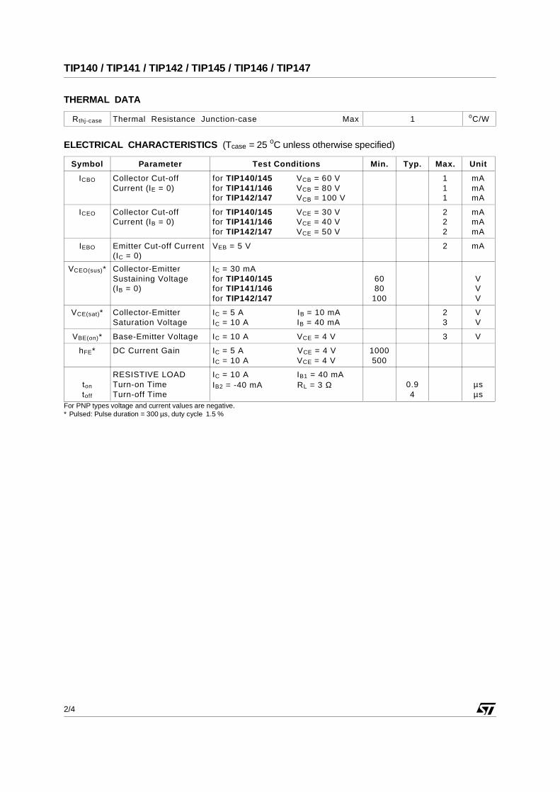
THERMAL DATA
Rthj-case Thermal Resistance Junction-case Max 1 oC/W
ELECTRICAL CHARACTERISTICS (Tcase = 25 oC unless otherwise specified)
Symbol Parameter Test Conditions Min. Typ. Max. Unit
ICBO Collector Cut-offCurrent (IE = 0)
for TIP140/145 VCB = 60 Vfor TIP141/146 VCB = 80 Vfor TIP142/147 VCB = 100 V
111
mAmAmA
ICEO Collector Cut-offCurrent (IB = 0)
for TIP140/145 VCE = 30 Vfor TIP141/146 VCE = 40 Vfor TIP142/147 VCE = 50 V
222
mAmAmA
IEBO Emitter Cut-off Current(IC = 0)
VEB = 5 V 2 mA
VCEO(sus)* Collector-EmitterSustaining Voltage(IB = 0)
IC = 30 mAfor TIP140/145for TIP141/146for TIP142/147
6080
100
VVV
VCE(sat)* Collector-EmitterSaturation Voltage
IC = 5 A IB = 10 mAIC = 10 A IB = 40 mA
23
VV
VBE(on)* Base-Emitter Voltage IC = 10 A VCE = 4 V 3 V
hFE* DC Current Gain IC = 5 A VCE = 4 VIC = 10 A VCE = 4 V
1000500
ton
toff
RESISTIVE LOADTurn-on TimeTurn-off Time
IC = 10 A IB1 = 40 mAIB2 = -40 mA RL = 3 Ω 0.9
4µsµs
For PNP types voltage and current values are negative.∗ Pulsed: Pulse duration = 300 µs, duty cycle 1.5 %
TIP140 / TIP141 / TIP142 / TIP145 / TIP146 / TIP147
2/4

DIM.mm inch
MIN. TYP. MAX. MIN. TYP. MAX.
A 4.7 4.9 0.185 0.193
C 1.17 1.37 0.046 0.054
D 2.5 0.098
E 0.5 0.78 0.019 0.030
F 1.1 1.3 0.043 0.051
G 10.8 11.1 0.425 0.437
H 14.7 15.2 0.578 0.598
L2 – 16.2 – 0.637
L3 18 0.708
L5 3.95 4.15 0.155 0.163
L6 31 1.220
R – 12.2 – 0.480
Ø 4 4.1 0.157 0.161
R
AC D
E
H
F
G
L6
¯
L3L2
L5
1 2 3
TO-218 (SOT-93) MECHANICAL DATA
P025A
TIP140 / TIP141 / TIP142 / TIP145 / TIP146 / TIP147
3/4

Information furnished is believed to be accurate and reliable. However, STMicroelectronics assumes no responsibility for the consequencesof use of such information nor for any infringement of patents or other rights of third parties which may result from its use. No license isgranted by implication or otherwise under any patent or patent rights of STMicroelectronics. Specification mentioned in this publication aresubject to change without notice. This publication supersedes and replaces all information previously supplied. STMicroelectronics productsare not authorized for use as critical components in life support devices or systems without express written approval of STMicroelectronics.
The ST logo is a trademark of STMicroelectronics
© 2000 STMicroelectronics – Printed in Italy – All Rights ReservedSTMicroelectronics GROUP OF COMPANIES
Australia - Brazil - China - Finland - France - Germany - Hong Kong - India - Italy - Japan - Malaysia - Malta - Morocco - Singapore - Spain - Sweden - Switzerland - United Kingdom - U.S.A.
http://www.st.com
TIP140 / TIP141 / TIP142 / TIP145 / TIP146 / TIP147
4/4