TIP-VBY1HS Data Sheet - solutions.inrevium.com · TABLE 8.1 PARAMETERIZATION TABLE ... TX_FORMA...
21
TIP-VBY1HS-DS Rev1.03 1 TIP-VBY1HS Data Sheet V-by-One ® HS Standard IP for Xilinx FPGA Rev.1.04 Tokyo Electron Device Ltd. DATA SHEET
Transcript of TIP-VBY1HS Data Sheet - solutions.inrevium.com · TABLE 8.1 PARAMETERIZATION TABLE ... TX_FORMA...

TIP-VBY1HS-DS
Rev1.03 1
Preliminary
TIP-VBY1HS
Data Sheet
V-by-One® HS Standard IP
for Xilinx FPGA
Rev.1.04
Tokyo Electron Device Ltd.
DATA SHEET

TIP-VBY1HS-DS
Rev1.03 2
Revision History
The following table shows the revision history for this document.
Revision Date Comments
Rev.1.0.0 2011/11/15 First release
Rev.1.0.2 2012/06/25 Kintex-7 Families Support
Rev.1.0.3 2015/12/04 Spartan-6 Families and Virtex-6 Families does not support
Artix-7 Families, Virtex-7 Families and KintexUltraScale Families Support
Rev.1.0.4 2016/05/13 Table 8.1 P_VNUM parameter fixed

TIP-VBY1HS-DS
Rev1.03 3
Table of Contents
1. Introduction ...................................................................................................................... 5
2. Features ........................................................................................................................... 5
3. References ...................................................................................................................... 5
4. Specification outline ......................................................................................................... 6
5. Functional Overview ........................................................................................................ 7
5.1. Transmitter part of the Core .......................................................................................... 7
5.2. Receiver part of the Core .............................................................................................. 9
6. I/O Signals ..................................................................................................................... 11
6.1. Common part of the Core ............................................................................................ 11
6.2. Transmitter part of the Core ........................................................................................ 11
6.3. Receiver part of the Core ............................................................................................ 13
7. Reference Clock ............................................................................................................ 15
7.1. Clock Construction ....................................................................................................... 15
7.2. Recommended Board Design..................................................................................... 16
8. Parameterization ............................................................................................................ 17
9. Verification ..................................................................................................................... 18
9.1. Simulation ...................................................................................................................... 18
10. Family Support ............................................................................................................. 19
11. Technical Support ........................................................................................................ 19
12. Licensing and Ordering Information ............................................................................. 20

TIP-VBY1HS-DS
Rev1.03 4
Schedule of Figures
FIGURE 5.1 TRANSMITTER PART OF THE CORE BLOCK DIAGRAM (INCLUDE GT) ....................................................... 7
FIGURE 5.2 TRANSMITTER PART OF THE CORE BLOCK DIAGRAM (WITHOUT GT) ...................................................... 8
FIGURE 5.3 RECEIVER PART OF THE CORE BLOCK DIAGRAM (INCLUDE GT) ............................................................. 9
FIGURE 5.4 RECEIVER PART OF THE CORE BLOCK DIAGRAM (WITHOUT GT) .......................................................... 10
FIGURE 7.1 TIP-VBY1HS CLOCK CONSTRUCTION .............................................................................................. 15
FIGURE 7.2 TRANSMITTER FPGA RECOMMENDED BOARD DESIGN....................................................................... 16
FIGURE 7.3 RECEIVER FPGA RECOMMENDED BOARD DESIGN ............................................................................ 16
FIGURE 9.1 BLOCK DIAGRAM FOR SIMULATION ..................................................................................................... 18
Schedule of Tables
TABLE 4.1 TIP-VBY1HS SPECIFICATION .............................................................................................................. 6
TABLE 6.1 COMMON PART I/O SIGNALS .............................................................................................................. 11
TABLE 6.2 TRANSMITTER PART I/O SIGNALS ....................................................................................................... 11
TABLE 6.3 TX DATA AND CONTROL MAPPING FOR BYTE MODE ................................................................................ 12
TABLE 6.4 RECEIVER PART I/O SIGNALS ............................................................................................................. 13
TABLE 6.5 RX DATA AND CONTROL MAPPING FOR BYTE MODE ............................................................................... 14
TABLE 8.1 PARAMETERIZATION TABLE ................................................................................................................ 17

TIP-VBY1HS-DS
Rev1.03 5
1. Introduction
V-by-One® HS standard has been developed by THine Electronics, Inc. to offer capabilities for Flat
Panel Display (FPD) markets that are requiring ever-higher frame rates and higher resolutions.
The TIP-VBY1HS Core provided by Tokyo Electron Device Ltd. (TED) is a high performance, flexible
solution for a high speed transmission of video signals designed to the V-by-One® HS standard for
the Xilinx FPGA.
State-of-the-art Kintex®-7 families, Virtex
®-7 families, Artix
®-7 families and Kintex
® UltraScale™
families are supported.
2. Features
Protocol compliant with V-by-One® HS 1.4 standard provided by THine Electronics, Inc.
Implementation of the Transmitter module or the Receiver one or both.
Supports 4, 8, 16, and 32 lanes operations.
Uses the GTP transceivers of Artix-7 families, the GTX transceivers of Kintex-7 families and the
GTH transceivers of Virtex-7 families and Kintex UltraScale families.
Supports up to 3.7125Gbps data rate per lane..
Elastic buffers and Lane alignment.
Data scrambling and Clock Data Recovery (CDR) to reduce EMI.
Variable settings of the driver swing, pre-emphasis.
Flexible implementation and package compatibility.
3. References
- V-by-One®HS Standard Version 1.4 (Dec 15, 2011) by THine Electronics, Inc.
- TIP-VBY1HS_UserManual
- 7 Series FPGAs GTX/GTH Transceivers (UG476)
- 7 Series FPGAs GTP Transceivers(UG482)
- UltraScale Architecture GTH Transceivers(UG576)
- Kintex-7 FPGA Data Sheet : DC and Switching Characteristics (DS182)
- Virtex-7 T and XT FPGAs Data Sheet: DC and AC Switching Characteristics(DS183)
- Artix-7 FPGAs Data Sheet: DC and AC Switching Characteristics(DS181)
Kintex UltraScale Architecture Data Sheet: DC and AC Switching Characteristics(DS892)

TIP-VBY1HS-DS
Rev1.03 6
4. Specification outline
Table 4.1 TIP-VBY1HS Specification
IP Facts
Core Specifics
Supported FPGA Family Kintex-7 Virtex-7 Artix-7 Kintex UltraScale
FPGA Speed Grade -3, -2, -1 Performance
(Serial Line Rate) 3.7125Gbps
Core Resources ( in case of Virtex-7 Synthesis design 4byte)
LANEs MGT FFs LUTs Block RAMs BUFGs PLLs
Transmitter
4 4 7,100 4,400 14
3(1) 1 (1) 8 8 12,400 6,900 28
16 16 24,800 13,700 56
32 32 55,100 33,200 112
Receiver
4 4 7300 3900 8
3 (1) 1 (1) 8 8 13,800 7,000 16
16 16 27,500 13,900 32
32 32 57,000 30,100 64
Core Highlights
Designed Verification RTL Test Bench
Provided with Core
Documentation Data Sheet
TIP-VBY1HS User Manual
Design File Formats RTL (IEEE P1376 encrypted)
Data format IP repository
Constraints File XDC(Xilinx Design Constraint)
Verification Verilog Test Bench
Design Tool Requirements
Synthesis and Implement Tools
Vivado® 2015.3
Simulation Mentor Graphics® ModelSim
® 10.4b and above
Support
Tokyo Electron Device Ltd.
(1) Number of the Clock resources (PLLs and BUFGs) will change according to the user logic, implementation and board circuit.

TIP-VBY1HS-DS
Rev1.03 7
5. Functional Overview
5.1. Transmitter part of the Core
In the first, the Transmitter part of the core allocates the video stream and control signals to the
Main links according to the number of the data lanes. Each Main Link transfers the allocated data
through the High-speed serial transceiver with framing, packet data mapping, scrambling, and
encoding.
The Transmitter part of the core also has a training function for the link start up with the receiver
side while checking the Hot plug and CDR Lock status signal.
In order to check the quality of the high-speed serial data lines, the Transmitter part of the core has
an operation mode in which they act as the bit error tester (BET) called “Field BET mode”.
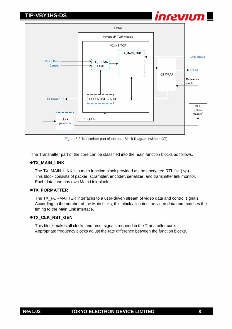
Figure 5.1 and Figure 5.2 show the function block diagram of the Transmitter part.
vbyone IP TOP module
VX1HS_TOP
TX_FORMATTER
TX_CLK_RST_GEN
TX_MAIN_LINK
GT_WRAP
Video Data
Control
TX_PXCLK_O
Link status
Reference clock
DATA
FPGA
PLL(Jitter
cleaner)
clock generater
INIT_CLK
Figure 5.1 Transmitter part of the core Block Diagram (include GT)
TIP-VBY1HS-DS
Rev1.03 8
vbyone IP TOP module
VX1HS_TOP
TX_FORMATTER
TX_CLK_RST_GEN
TX_MAIN_LINK
GT_WRAP
Video Data
Control
TX_PXCLK_O
Link status
Reference clock
DATA
FPGA
PLL(Jitter
cleaner)
clock generater
INIT_CLK
Figure 5.2 Transmitter part of the core Block Diagram (without GT)
The Transmitter part of the core can be classified into the main function blocks as follows.
TX_MAIN_LINK
The TX_MAIN_LINK is a main function block provided as the encrypted RTL file (.vp) .
This block consists of packer, scrambler, encoder, serializer, and transmitter link monitor.
Each data lane has own Main Link block.
TX_FORMATTER
The TX_FORMATTER interfaces to a user-driven stream of video data and control signals.
According to the number of the Main Links, this block allocates the video data and matches the
timing to the Main Link interface.
TX_CLK_RST_GEN
This block makes all clocks and reset signals required in the Transmitter core.
Appropriate frequency clocks adjust the rate difference between the function blocks.

TIP-VBY1HS-DS
Rev1.03 9
5.2. Receiver part of the Core
The Receiver part of the Core has a symmetrical function with the Transmitter part of the core.
Each Main Links receives the data from the transmitter side through the High-speed serial
transceiver and regenerates the allocated data with decoding, de-scrambling, packet data
un-mapping, and de-framing. In the end, these framing data from the Main Links combined to
regenerate the original stream of video data and control signals.
The Receiver core also has a training function for the link start up with the transmitter side while
generating the Hot plug and CDR Lock status signal.
In order to check the quality of the high-speed serial data lines, the Receiver part of the core has an
operation mode in which they act as the bit error tester (BET) called “Field BET mode”.
Figure 5.3 and Figure 5.4 show the function block diagram of the Receiver part.
vbyone IP TOP module
VX1HS_TOP
RX_DEFORMATTER
RX_CLK_RST_GEN
RX_MAIN_LINK
GT_WRAP
Video Data
Control
RX_PXCLK
Link status
Reference clock
DATA
FPGA
PLL(Jitter
cleaner)
clock generater
INIT_CLK
Figure 5.3 Receiver part of the core Block Diagram (include GT)

TIP-VBY1HS-DS
Rev1.03 10
vbyone IP TOP module
VX1HS_TOP
RX_DEFORMATTER
RX_CLK_RST_GEN
RX_MAIN_LINK
GT_WRAP
Video Data
Control
RX_PXCLK
Link status
Reference clock
DATA
FPGA
PLL(Jitter
cleaner)
clock generater
INIT_CLK
Figure 5.4 Receiver part of the core Block Diagram (without GT)
The Receiver part of the core can be classified into the main function blocks as follows.
RX_MAIN_LINK
The RX_MAIN_LINK is a main function block provided as the encrypted RTL file (.vp) .
This block consists of unpacker, de-scrambler, decoder, de-serializer, and receiver link monitor.
Each data lane has own Main Link block.
RX_DEFORMATTER
RX_DEFORMATTER matches the skew of the packet data from the Main Links and regenerates
the user-driven stream of video data and control signals from the allocated data in the Main Links.
RX_CLK_RST_GEN
This block makes all clocks and reset signals required in the Receiver core from the recovery
clock from the transceiver in Main block.
Appropriate frequency clocks adjust the rate difference between the function blocks and
regenerate the pixel clock of the Transmitter side.

TIP-VBY1HS-DS
Rev1.03 11
6. I/O Signals
6.1. Common part of the Core
Table 6.1 Common Part I/O Signals
Signal Name Direction Polarity Description Dedicated External
Pin
REFCLK_P[(P_LNUM-1)/8:0] Input ↑ MGTCLK for MGT Positive ✔
REFCLK_N[(P_LNUM-1)/8:0] input ↓ MGTCLK for MGT Negative ✔
INIT_CLK input ↑ Free run clock 7series : 74.25MHz Kintex UltraScale : 148.5MHz
6.2. Transmitter part of the Core
Table 6.2 Transmitter Part I/O Signals
Signal Name Direction Polarity Description Dedicated External
Pin
TX_PDN Input ‘L’ Power Down
Main Link Interface
TX0_P [P_LNUM-1:0] Output - High-speed serial data lanes positive
✔
TX0_N [P_LNUM-1:0] Output - High-speed serial data lanes negative
✔
TX_HTPDN Input ‘L’ Hot plug detect ✔
TX_LOCKN Input ‘L’ Lock detect ✔
User Data Interface
TX_PXCLK Input ↑ Pixel Clock
TX_VSYNC[P_VNUM-1:0] Input ‘L’ Vertical sync pulse
TX_HSYNC[P_VNUM-1:0] Input ‘L’ Horizontal sync pulse
TX_DE[P_VNUM-1:0] Input ‘H’ Video data enable
TX_D [40*P_VNUM-1:0] (1) Input - Video data
TX_CTL[24*P_VNUM-1:0] (2) Input - Control data
Mode Setting
TX_ DRV [3:0] Input - Drive Strength Control
TX_ PRE [4:0] Input - Pre-Emphasis Control
TX_FIELD_BET Input ‘H’ Field BET Mode Enable
Status Signal
TX_ RDY output ‘H’ Link Status Ready
for without GT
TX_ TXUSERCLK2_IN input ↑ Clock from MGT
TX_RESET_DONE_IN input ‘H’ Reset done from MGT
TX_POWERDOWN_OUT[1:0] output ‘H’ Power down to MGT
LNX_TXCHARISK_OUT [2*P_LNUM-1:0]
output - K character to MGT
LNX_TXDATA_OUT [16*P_LNUM-1:0]
output - Data to MGT
(1) Video data width is dependent on the Byte Mode setting with byte boundary (24 / 32 / 40 bits) as following table.
(2) Control data width is dependent on the Byte Mode setting with byte boundary (8 / 16 / 24 bits) as following table.

TIP-VBY1HS-DS
Rev1.03 12
Table 6.3 tx data and control mapping for byte mode
Byte Mode DI [39:0] CTL [23:0]
3 23:0 7:0
4 31:0 15:0
5 39:0 23:0

TIP-VBY1HS-DS
Rev1.03 13
6.3. Receiver part of the Core
Table 6.4 Receiver Part I/O Signals
Signal Name Direction Polarity Description Dedicated External
Pin
PDN Input ‘L’ Power Down
RX_RECCLK output ↑ Recovery clock out for External PLL (optional)
✔
Main Link Interface
RX0_P [P_LNUM-1:0] Input - High-speed serial data lanes positive
✔
RX0_N [P_LNUM-1:0] Input - High-speed serial data lanes negative
✔
RX_HTPDN Output ‘L’ Hot Plug Detect ✔
RX_LOCKN Output ‘L’ Lock Detect ✔
User Data Interface
RX_PXCLK Output ↑ Pixel Clock
RX_VSYNC Output ‘L’ Vertical sync pulse
RX_HSYNC Output ‘L’ Horizontal sync pulse
RX_DE Output ‘H’ Video data enable
RX_DO [40*P_VNUM-1:0] (1)
Output - Video Data
RX_CTL [24*P_VNUM-1:0] (2) Output - Control Data
Mode Setting
RX_FIELD_BET Input ‘H’ Field BET Mode Enable
Status Signal
RX_FIELD_BET_ERR Output ‘H’ Filed BET mode Check Error Status
for without GT
RX_USERCLK2_IN input ↑ Clock from MGT
RX_RESETDONE_IN input ‘H’ Reset done from MGT LNX_RXDATA_IN [16*P_LNUM-1:0]
input - Data from MGT
LNX_RXDISPERR_IN [2*P_LNUM-1:0]
input - Disparity error from MGT
LNX_RXNOTINTABLE_IN [2*P_LNUM-1:0]
input - Not in table from MGT
LNX_RXBYTEISALIGNED_IN [P_LNUM-1:0]
input - Byte is aligned from MGT
LNX_RXCOMMADET_IN [P_LNUM-1:0]
input - Comma detect from MGT
LNX_RXCHARISCOMMA_IN [2*P_LNUM-1:0]
input - Comma character from MGT
LNX_RXCHARISK_IN [2*P_LNUM-1:0]
input - K character from MGT
RXPOWERDOWN_OUT [1:0]
output ‘H’ Power down to MGT
LNX_RXENMCOMMAALIGN_OUT [P_LNUM-1:0]
output ‘H’ Comma minus to MGT
LNX_RXENPCOMMAALIGN_OUT [P_LNUM-1:0]
output ‘H’ Comma plus to MGT
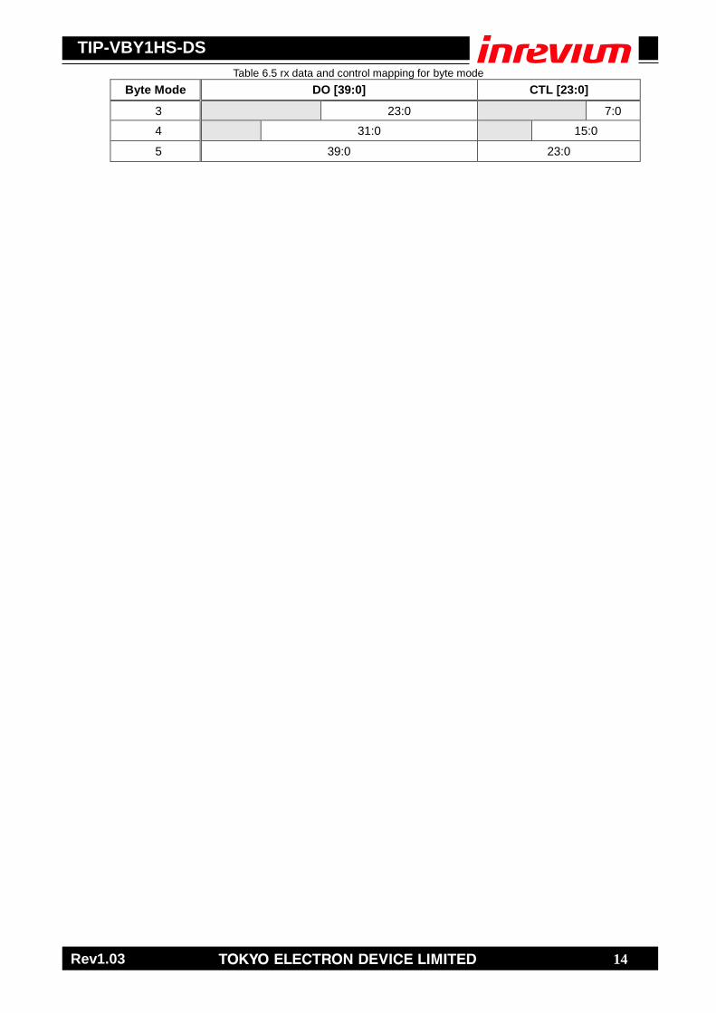
(1) Video data width is dependent on the Byte Mode setting with byte boundary (24 / 32 / 40 bits) as following table.
(2) Control data width is dependent on the Byte Mode setting with byte boundary (8 / 16 / 24 bits) as following table.
TIP-VBY1HS-DS
Rev1.03 14
Table 6.5 rx data and control mapping for byte mode
Byte Mode DO [39:0] CTL [23:0]
3 23:0 7:0
4 31:0 15:0
5 39:0 23:0

TIP-VBY1HS-DS
Rev1.03 15
TX_PXCLK
REFCLK_PREFCLK_N
TransmitterCore
ReceiverCore
REFCLK_P/N should be generated from PXCLK (Frequency locking is required)
REFCLK_PREFCLK_N
RX_PXCLK
Frequency deflection of REFCLK_P/N is limited to the transmission rate
7. Reference Clock
7.1. Clock Construction
Besides the pixel clock, TIP-VBY1HS Transmitter and Receiver Core require the high quality
reference clock (REFCLK_P/N port) conforming to the MGT transceiver’s specification.
Especially, the REFCLK of the Receiver Core side is important because its frequency deviation is
limited to the transmission rate of the Data Lane.
In addition, REFCLK is recommended to be supplied by the differential pair port and to be satisfied
the specification shown in FPGA data sheets.
Generally, frequency of the REFCLK is same to the pixel clock, it is also possible to use the
REFCLK of the frequency different from the pixel clock by setting the PLL of the MGT
Transceivers.
Figure 7.1 TIP-VBY1HS Clock Construction

TIP-VBY1HS-DS
Rev1.03 16
Pixel Clock
Transmitter FPGA
VCXO PLL Clock Synthesizer& Jitter Cleaner REFCLK_P/N
PXCLK
M/D
MGTREFCLK-pin
TransmitterMain Links
・・・
HTPDNLOCKN
VDL
TXn_PTXn_N
PLL
ReceiverMain Links
RXn_PRXn_N
HTPDNLOCKN
・・・
Open-drain outputMGTREFCLK-pin
VCXO PLL Clock Synthesizer& Jitter CleanerREFCLK_P/N
RECCLK M/D
PXCLK
CLKOUT
X’tal
Receiver FPGA
7.2. Recommended Board Design
Following Figures show the recommended REFCLK construction of the board.
Transmitter side
Figure 7.2 shows the construction of the Transmitter side.
It has the external PLL IC to clean-up the jitter of the pixel clock or synthesize the frequency that
is required for the REFCLK input.
“M/D” block in the FPGA generates the appropriate frequency to the external PLL IC’s input, so
this block is optional.
Receiver side
Figure 7.3 shows the construction of the Receiver side.
In addition to the same purpose as the Transmitter side, the Receiver side has the external VCXO
PLL IC to generate the initial REFCLK of the frequency that is required for the Clock Data
Recovery (CDR) of the MGT Transceivers. After CDR is locked, this VCXO PLL should be
phase-locked to the recovery clock and generate the REFCLK of frequency that is completely the
same as the Transmitter side.
(Note) If you use TB-FMCH-VX1-AD board, you should drive High/Low about RX_HTPDN and
RX_LOCKN signals, because the board has tri-state buffer IC.
Figure 7.2 Transmitter FPGA Recommended Board Design
Figure 7.3 Receiver FPGA Recommended Board Design

TIP-VBY1HS-DS
Rev1.03 17
8. Parameterization
Following Table shows the representative parameter of the IP core.
Table 8.1 Parameterization Table
Parameter Name Values Description
C_FAMILY
artix7 kintex7 virtex7 kintexu
Target FPGA family
P_GT_WRAP_IN 0, 1 Include MGT enable
0:without GT 1:include GT
P_BYTE_MD 0, 1, 2
Byte width of video data and control signal (Byte-mode) 0:3Byte mode 1:4Byte mode 2:5Byte mode
P_TXRX_OFFSEL
1, 2, 3
Activate Transmitter or Receiver or both 3: Transmitter and Receiver both on 2: only Receiver on 1: only Transmitter on
P_RX_OD 0, 1 Open Drain enable (RX_HTPDN and RX_LOCKN)
0:disable(High and Low) 1:enable(High-Z and Low)
P_LNUM 4, 8, 16, 32 Number of Lanes
P_MNUM 1, 2, 4, 8 Number of mapping Lanes
P_VNUM P_LNUM / P_MNUM Number of video signal channel

TIP-VBY1HS-DS
Rev1.03 18
9. Verification
The TIP-VBY1HS Core has been verified with the RTL simulation and hardware validation of
connectivity test by THine Electronics, Inc.
9.1. Simulation
All byte-modes and data lane numbers are tested by following construction.
TB_SIM_MODEL
dut_tx
dut_txrx
dut_rx
Video in TX_P/N RX_P/N
RX_P/N TX_P/NVideo out Video in
Video out
Figure 9.1 block diagram for simulation

TIP-VBY1HS-DS
Rev1.03 19
10. Family Support
The TIP_VBY1HS Core was designed to target the Kintex-7, Virtex-7, Artix-7 and Kintex UltraScale
FPGA families.
- ~3.7125Gbps data rate per lane (same as the standard)
Kintex-7 all speed grade
Virtex-7 all speed grade
Artix-7 all speed grade
Kintex UltraScale all speed grade
Fllowing equation shows how to determine the data rate of the lane (Gbps).
Example
Byte-mode = 4byte, Pixel Clock frequency = 148.5MHz, Number of data lanes = 2
Data rate per lane = (32bit × 148.5MHz × 1.25) / 2 = 2.97Gbps
11. Technical Support
Tokyo Electron Device Ltd. (TED) provides technical support for this IP Core when used as described
in the product documentation. TED cannot guarantee timing, functionality, or support of product if
implemented in devices that are not defined in the documentation, if customized beyond that allowed
in the product documentation, of if changes are made to any section of the design labeled DO NOT
MODIFY.
TED also offers a reference design with their evaluation board and a contract-based development
service for customized design or additional function design (ex. more than 32 data lanes for Virtex-7).
fDataRate = ( BITByteMode × fPixelClk × 1.25(8B/10B) ) / NLane

TIP-VBY1HS-DS
Rev1.03 20
12. Licensing and Ordering Information
Kintex-7 TX IP
Licensing : ipted_TIP_VBY1HS_K7TX_PROJ
Ordering : TIP-VBY1HS-K7TX-PROJ
RX IP
Licensing : ipted_TIP_VBY1HS_K7RX_PROJ
Ordering : TIP-VBY1HS-K7RX-PROJ
TX-RX IP
Licensing : ipted_TIP_VBY1HS_K7TX_PROJ and
ipted_TIP_VBY1HS_K7RX_PROJ
Ordering : TIP-VBY1HS-K7-PROJ
Virtex-7 TX IP
Licensing : ipted_TIP_VBY1HS_V7TX_PROJ
Ordering : TIP-VBY1HS-V7TX-PROJ
RX IP
Licensing : ipted_TIP_VBY1HS_V7RX_PROJ
Ordering : TIP-VBY1HS-V7RX-PROJ
TX-RX IP
Licensing : ipted_TIP_VBY1HS_V7TX_PROJ and
ipted_TIP_VBY1HS_V7RX_PROJ
Ordering : TIP-VBY1HS-V7-PROJ
Artix-7 TX IP
Licensing : ipted_TIP_VBY1HS_A7TX_PROJ
Ordering : TIP-VBY1HS-A7TX-PROJ
RX IP
Licensing : ipted_TIP_VBY1HS_A7RX_PROJ
Ordering : TIP-VBY1HS-A7RX-PROJ
TX-RX IP
Licensing : ipted_TIP_VBY1HS_A7TX_PROJ and
ipted_TIP_VBY1HS_A7RX_PROJ
Ordering : TIP-VBY1HS-A7-PROJ
Kintex UltraScale TX IP
Licensing : ipted_TIP_VBY1HS_KUTX_PROJ
Ordering : TIP-VBY1HS-KUTX-PROJ
RX IP
Licensing : ipted_TIP_VBY1HS_KURX_PROJ
Ordering : TIP-VBY1HS-KURX-PROJ
TX-RX IP
Licensing : ipted_TIP_VBY1HS_KUTX_PROJ and
ipted_TIP_VBY1HS_KURX_PROJ
Ordering : TIP-VBY1HS-KU-PROJ

TIP-VBY1HS-DS
Rev1.03 21
Inrevium Company URL: http://solutions.inrevium.com/
http://solutions.inrevium.com/jp
E-mail: [email protected] HEAD Quarter: Yokohama East Square, 1-4 Kinko-cho, Kanagawa-ku, Yokohama City,
Kanagawa, Japan 221-0056 TEL: +81-45-443-4031 FAX: +81-45-443-4063