Ting-Chi Lee OES, ITRI 11/07/2005 GaN-based Heterostructure Field-Effect Transistors.
92
Ting-Chi Lee OES, ITRI 11/07/2005 GaN-based Heterostructure Field-Effect Transistors
-
Upload
anna-higgins -
Category
Documents
-
view
222 -
download
1
Transcript of Ting-Chi Lee OES, ITRI 11/07/2005 GaN-based Heterostructure Field-Effect Transistors.

Ting-Chi LeeOES, ITRI11/07/2005
GaN-based Heterostructure Field-Effect Transistors

Outline
Introduction to GaN ICP etching of GaN Low resistance Ohmic contacts to n-GaN Narrow T-gate fabrication on GaN Polarization effect in AlGaN/GaN HFETs Thermal effect of AlGaN/GaN HFETs Conclusion

Introduction Unique material properties of GaN
Wide bandgap, 3.4 eV at RT High breakdown field, 3 MV/cm High electron saturation velocity, 1.3x107 cm/s Excellent thermal stability Strong polarization effect


Introduction GaN-based devices
Great achievement in blue LEDs and laser diodes Potential microwave high power devices Next generation wireless communication system, especially
in the base station power amplifiers, high Vbk is required
Next generation wireless communication Access multi-media information using cell phones or PDAs
at any time anywhere High-efficiency base station PAs Present base station PAs: Si LDMOS, low efficiency

Device Power Performance vs. Frequency
0.1
1
10
100
1000
10 100
HBT
SiC
pHEMT
GaN
Frequency (GHz)

The Wide Band Gap Device Advantages
GaN HEMT and Process

Suitable Specifications for GaN-based Power Devices

Ron of GaN HEMT Switches

• For high-power switching applications GaN schottky diodes GaN p-i-n diodes GaN HEMT-based switching devices GaN MOSHFET-based switching devices
• For microwave power amplifications GaN Schottky diode AlGaN/GaN HEMTs AlGaN/GaN MOSHFETs GaN-based microwave circuits
• For pressure sensor application AlGaN/GaN HEMTs
GaN-based devices for various applications

R & D activity in GaN HFET Company
RF Micro Devices, Cree Inc., Sensor Electronic Technology, ATMI Epi wafers for GaN FET
Lab. USA: US Naval Research Lab., Hughes Research Lab., Lucent
Technologies Bell Lab., TRW, nitronex USA: Cornell U., UCSB, RPI, U. Texas, USC, NCSU Germany: Water-Schottky Institute, DaimlerChrysler lab. Sweden: Chalmers U., Linkopings U., Japan: Meijo U., NEC and Sumitomo
Military contracting lab. Raytheon, GE, Boeing, Rockwell, TRW, Northrop Grumman, BAE
Systems North America
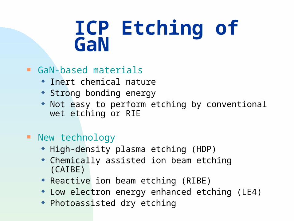
ICP Etching of GaN
GaN-based materials Inert chemical nature Strong bonding energy Not easy to perform etching by conventional wet
etching or RIE
New technology High-density plasma etching (HDP) Chemically assisted ion beam etching (CAIBE) Reactive ion beam etching (RIBE) Low electron energy enhanced etching (LE4) Photoassisted dry etching

ICP Etching of GaN
High density plasma etching (HDP) Higher plasma density The capability to effectively decouple the ion
energy and ion density
Inductively coupled plasma (ICP) Electron cyclotron resonance (ECR) Magnetron RIE (MRIE)
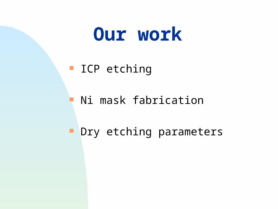
Our work
ICP etching
Ni mask fabrication
Dry etching parameters

Ni mask fabrication
Suitable etching mask for ICP etching of GaN PR, Ni and SiO2
Ni mask fabrication Wet chemical etching by HNO3: H2O (1:1) Lift-off

Ni mask fabrication
Wet etching
20 um
Rough edgePoor dimension control
Lift-off
20 um
Smooth edgeGood dimension control
Ni
Ni
PR

Dry etching parameters: bias power
0 5 10 15 20 25 30
0
500
1000
1500
2000
2500
3000
3500
Etc
hing
rat
e (A
/min
.)
Bias power (W)
ICP 300WPressure 15mtorrCl 50sccmAr 5 sccm
Larger bias power-Increase the kinetic energy of incident ions-Enhance physical ion bombardment
-More efficient bond breaking and desorption of etched products

Dry etching parameters: bias power
Bias power: 5 w
Bias power: 30 w
Bias power: 10 w
Bias power: 20 w
Ni: 2000 ÅGaN: 2 um

Dry etching parameters: Ar flow rate
Higher Ar flow rate-Increase the density of incident Ar ions-Enhance physical ion bombardment
Ar flow rate> 15 sccm-Cl2/Ar flow ratio decrease
0 5 10 15 20 25 303300
3320
3340
3360
3380
3400
3420
3440
etc
h r
ate
(A
/min
)
Ar flow rate (sccm)
Samco ICPICP 300wBias 30wPressure 15mTorrCl 50sccm

Ar flow rate: 5 sccm
Ar flow rate: 25 sccm
Ar flow rate: 15 sccm
Ar flow rate: 20 sccm
Dry etching parameters: Ar flow rate
Ni: 2000 ÅGaN: 2 um

Dry etching parameters: Cl2 flow rate
Higher Cl flow rate-Generate more reactive Cl radicals to participate in the surface chemical reaction
10 20 30 40 502600
2800
3000
3200
3400
3600
Etc
hin
g r
ate
(A
/min
.)
Cl2 flow rate (sccm)
ICP power: 300 WBias power: 30 Wpressure: 15 mtorrAr flow: 5 sccm

Cl flow rate: 10 sccm
Cl flow rate: 50 sccm
Cl flow rate: 20 sccm
Cl flow rate: 30 sccm
Dry etching parameters: Cl2 flow rate
Ni: 2000 ÅGaN: 2 um

Summary
Good Ni mask fabrication by lift-off
Dry etching parameters Bias power Ar flow rate Cl2 flow rate
Smooth etched surface and vertical sidewall profile

Low resistance Ohmic contacts to n-GaN
GaN-based materials Wide bandgap Not easy to obtain low resistance Ohmic contacts
Approaches to improve the contact resistance Select proper contact metal: Ti, Al, TiAl, TiAlTiAu,… Surface treatment: HCl, HF, HNO3: HCl (1:3),…
Plasma treatment: Cl2/Ar, Cl2, Ar, …

Our work
Plasma treatment n-GaN with Nd=8.7x10¹⁶, 3.3x1018 cm-3
Cl2/Ar and Ar plasma
Thermal stability issue
Forming gas ambient treatment

Plasma treatment
n-GaN
sapphire
n-GaN
sapphire
n+-GaN
Plasma treatment -> create N vacancies (native donors) -> increase surface electron concentration
Cl2/Ar or Ar plasma

Plasma treatment: Cl2/Ar, ArND=8.7x1016 cm-3
No. 1 2 3 4 5 6 7 8 9
ICP power (w)Bias power (w) Pressure (mtorr)Cl2 flow (sccm)
Ar flow (sccm)Time (min.)
------
3005
1550301
3005
1550102
3005
1550152
3005
1550202
3005
1550302
3005
15-
101
3005
15-
301
3005
15-
501
Rc (Ω mm)‧ρs (Ω/□)
ρc (Ω cm‧ 2)
0.638621.0
6.6
0.614656.3
5.7
0.48692.2
3.4
0.45696.3
2.8
0.21668.30.68
0.28671.5
1.2
0.8767311
0.57649.3
5.0
0.38030.87
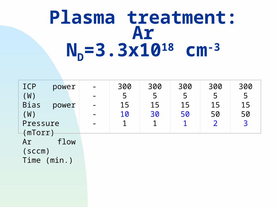
Plasma treatment: ArND=3.3x1018 cm-3
ICP power (W)Bias power (W)Pressure (mTorr)Ar flow (sccm)Time (min.)
-----
3005
15101
3005
15301
3005
15501
3005
15502
3005
15503
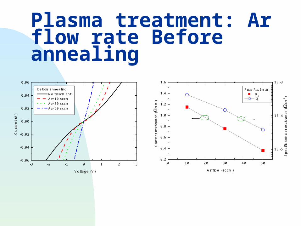
Plasma treatment: Ar flow rate Before annealing
-3 -2 -1 0 1 2 3-0.06
-0.04
-0.02
0.00
0.02
0.04
0.06
Cur
rent
(A
)
Voltage (V)
before annealing No treatment Ar=10 sccm Ar=30 sccm Ar=50 sccm
0 10 20 30 40 500.2
0.4
0.6
0.8
1.0
1.2
1.4
1.6
Co
nta
ct r
esi
sta
nce
(-
mm
)
Ar flow (sccm)
Pure Ar, 1min. R
C
1E-5
1E-4
1E-3
Sp
eci
fic c
on
tact
re
sist
an
ce (-
cm2 )
C

Plasma treatment: Ar flow rate After annealing
-1.0 -0.5 0.0 0.5 1.0-0.06
-0.04
-0.02
0.00
0.02
0.04
0.06
Cur
rent
(A
)
Voltage (V)
After annealing No treatment Ar=10 sccm Ar=30 sccm Ar=50 sccm
0 10 20 30 40 500.08
0.10
0.12
0.14
0.16
0.18
0.20Pure Ar,1min.
RC
Co
nta
ct r
esi
sta
nce
(-
mm
)
Ar flow (sccm)
1E-6
1E-5
C
no
tre
atm
en
t
Sp
eci
fic c
on
tact
re
sist
an
ce (-
cm2 )

Plasma treatment: time
-3 -2 -1 0 1 2 3
-0.06
-0.04
-0.02
0.00
0.02
0.04
0.06
Cur
rent
(A
)
Voltage (V)
Before annealing No treatment Ar=50, 1min. Ar=50, 2min. Ar=50, 3min.
-1.0 -0.5 0.0 0.5 1.0-0.06
-0.04
-0.02
0.00
0.02
0.04
0.06
Cur
rent
(A
)
Voltage (V)
After annealing No treatment Ar=50, 1min. Ar=50, 2min. Ar=50, 3min.

Plasma treatment: time
0.0 0.5 1.0 1.5 2.0 2.5 3.0
0.10
0.12
0.14
0.16
0.18
0.20
Pure Ar,50sccm R
Cn
o tr
ea
tme
nt
Co
nta
ct r
esi
sta
nce
(-
mm
)
Etching time (min.)
1E-6
1E-5
C
Sp
eci
fic c
on
tact
re
sist
an
ce(
-cm
2 )

Thermal stability issue
Important for devices Several studies on the thermal stability of Ohmic
contacts to n-GaN have been performed
Thermal stability of plasma-treated Ohmic contacts to n-GaN If the damages created or defects generated by plasma
treatment have any effect on the device reliability ?? Thermal aging tests at different temperatures for 2h were
performed to observe it

Thermal aging tests: N2 ambient
0 50 300 400 500 600
1E-6
1E-5
1E-4
Spe
cific
con
tact
res
ista
nce
(-c
m2 )
Temperature (0 C)
N2 ambient
No treatment Cl
2/Ar=50/20, 2min.
Cl2/Ar=50/30, 1min.
0 50 300 400 500 600
1E-6
1E-5
1E-4
Sp
eci
fic c
on
tact
re
sist
an
ce (-
cm2 )
Temperature (0 C)
N2 ambient
No treatment Ar=10 sccm, 1 min. Ar=50 sccm, 1 min.

Thermal aging tests: Air ambient
0 50 300 400 500 600
1E-6
1E-5
1E-4
S
pe
cific
con
tact
res
ista
nce
(-
cm2 )
Temperature (0 C)
Air ambient No treatment Cl
2/Ar=50/30, 2 min.
Ar=30sccm, 1 min.
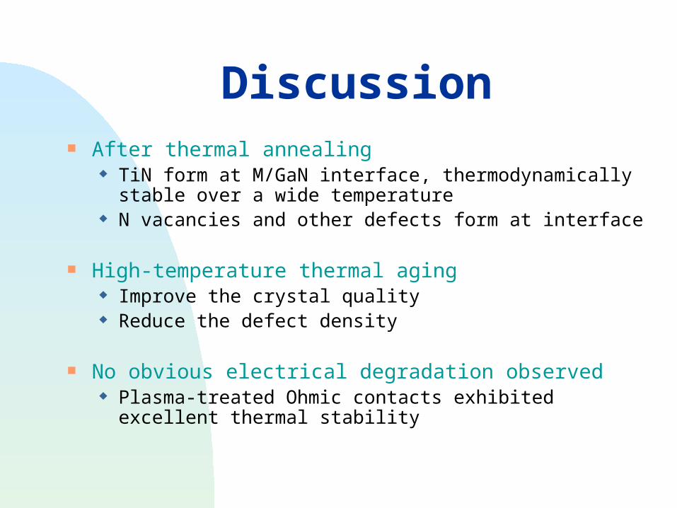
Discussion After thermal annealing
TiN form at M/GaN interface, thermodynamically stable over a wide temperature
N vacancies and other defects form at interface
High-temperature thermal aging Improve the crystal quality Reduce the defect density
No obvious electrical degradation observed Plasma-treated Ohmic contacts exhibited excellent
thermal stability

Forming gas ambient treatment
Thermal annealing in N2 ambient for nitride processing To avoid hydrogen passivation of dopants Especially for p-GaN
Forming gas annealing ambient Better reduction capability due to the H2
Reduce the oxidation reaction of metal at high T Cause carrier reduction of n-GaN due to the H
passivation ??
Forming gas ambient treatment
-1.0 -0.5 0.0 0.5 1.0-0.06
-0.04
-0.02
0.00
0.02
0.04
0.06
Cur
rent
(A
)
Voltage (V)
Forming gas ambient No treatment Ar=10 sccm Ar=30 sccm Ar=50 sccm
0 10 20 30 40 501E-6
1E-5
no
tre
atm
en
t
Sp
eci
fic c
on
tact
re
sist
an
ce (-
cm2 )
Ar flow (sccm)
Annealing ambient N
2 gas
Forming gas

Summary
Proper plasma treatment by Cl2/Ar or Ar Very effective in the improvement of contact resistance
Thermal stability issue Plasma-treated Ohmic contacts to n-GaN exhibited
excellent thermal stability
Forming gas ambient treatment No electrical degradation observed Even lower contact resistance obtained

Narrow T-gate fabrication on GaN
To realize high performance devices especially for high-frequency application
Conventional approach A high accelerating voltage of around 40-50 kV Much reduced forward scattering effect
A lower accelerating voltage for e-beam lithography Less backscattering from the substrate Lower doses needed Much reduced radiation damage But larger forward scattering effect

Our work
E-beam system
E-beam resist processing PMMA (120 nm)/Copolymer (680 nm)
Narrow T-gate fabrication using a lower accelerating voltage, 15 kV Writing pattern design Especially for the reduction of forward scattering with a
lower accelerating voltage

E-beam system
JEOL 6500 SEM + nano pattern generation system (NPGS) Max. acceleration voltage: 35 kV Beam current: tens of pA ~ 1 nA Thermal field emission (TFE) gun
Thermal field emission gun Large beam current Good beam current stability

Bi-layer PMMA/Copolymer process

Write strategy
Central stripe (50 nm): foot exposureSide stripe (75 nm): head exposureSpacing between the central stripe and the side stripe: key point

Foot width v.s. central dose
140 150 160 170 180 190 200
50
100
150
200
F
oo
t w
idth
(n
m)
Central dose (C/cm2)

40 nm Narrow T-gate

Discussion
As the spacing between the central stripe and the side stripe<< stripe width Sub 100 nm T-gate can be easily obtained Forward scattering effect was dramatically
improved Thus side exposure influences significantly the
final e-beam energy density profile
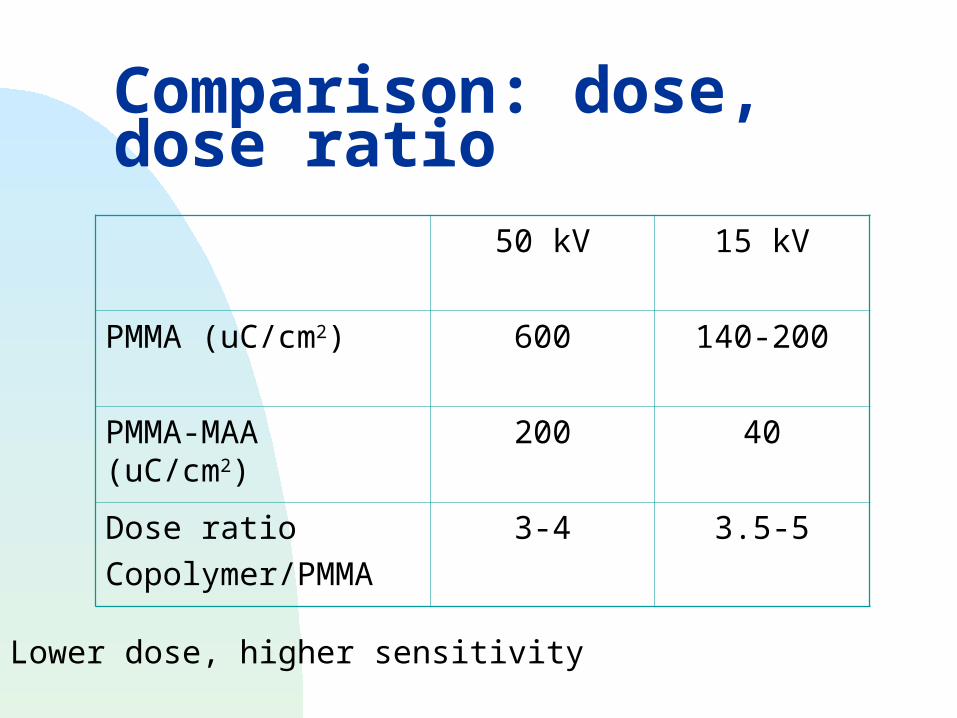
Comparison: dose, dose ratio
50 kV 15 kV
PMMA (uC/cm2) 600 140-200
PMMA-MAA (uC/cm2) 200 40
Dose ratio
Copolymer/PMMA
3-4 3.5-5
Lower dose, higher sensitivity
Summary
Narrow T-gate fabrication using a lower accelerating voltage of 15 kV is practical
Specially designed writing pattern Can significantly improve the forward scattering
problem with a lower accelerating voltage
Lower doses are needed for a lower accelerating voltage

Polarization effect in AlGaN/GaN HFETs
Design rules for realizing high performance GaN HFETs
High Al content AlGaN/GaN heterostructure Crystal structure Polarization-induced sheet charge, 2DEG Difficulties in the growth of AlGaN

High performance GaN HFETs
In addition to develop device processing technologies
Design rules High sheet charge density High carrier mobility Maintain high breakdown voltage
-> high Al composition AlGaN/GaN heterostructures

Higher band discontinuity Better carrier confinement Al=0.3, Ec=0.5 eV
Higher spontaneous polarization and piezoelectric effect Higher 2DEG sheet charge density
Higher bandgap of AlGaN higher breakdown field
High Al composition AlGaN/GaN heterostructures

Crystal structure and polarity JAP, 1999 Wurtzite crystal
structure Hexagonal Bravais
lattice (a, c, u) Both spontaneous
and piezoelectric polarization
Polarity
Ga-face: MOCVD or PIMBEN-face: PIMBE only

Polarization, polarization-induced sheet charge and formation of 2DEG
Ga-face N-face

Comparison of calculated and measured 2DEG ns
AlGaN: 200Å, ■/□: undoped/doped
Difficulties in the growth of AlGaN
Atomically smooth surface is not easy to obtain, especially in high Al content
Local variation in the alloy composition Strain in the AlGaN layer due to the lattice mismatch
bet. AlGaN and GaN Formation of structural defects Island growth mode Electrical property of heterostructure, piezoelectric effect
-> decrease in electron mobility with high Al composition
Our work
Design AlGaN/GaN heterostructures with different Al compositions, different AlGaN thickness and modulation-doping
Surface morphology
Electron transport properties
Device characteristics

Structure: Al=0.17
i-AlGaN 18 nm(Al=0.17)
i-GaN 3 µm
Buffer layer
Sapphire
Undoped Undoped
i-AlGaN 50 nm(Al=0.17)
i-GaN 3 µm
Buffer layer
Sapphire

Structure: Al=0.3
i-AlGaN 28 nm(Al=0.3)
i-GaN 3 µm
Buffer layer
Sapphire
i-AlGaN 5 nm
n-AlGaN: 5E18 20 nm
i-AlGaN 3 nm
i-GaN 3 µm
Buffer layer
Sapphire
Undoped Modulation-doped

Surface morphology: Al=0.17Top AlGaN: 18 nmUndoped AlGaN/GaN structure
Step flow structureRMS: 0.176 nm
Other location0.108 nm0.161 nm
Top AlGaN: 50 nmUndoped AlGaN/GaN structure
Step flow structureRMS: 0.176 nm

undoped AlGaN/GaN structure
Step flow structureRMS: 0.096 nmContact mode
Surface morphology: Al=0.3
Modulation-doped AlGaN/GaN structure
Step flow structureRMS: 0.131 nmContact mode

Discussion
Surface morphology Step-like structure Surface roughness ~ 0.15 nm Very smooth surface, indicating good
crystal quality Comparable to previous reports
Step like

Hall data: Al composition
100 200 300 400 5000.0
0.2
0.4
0.6
0.8
1.0
1.2
1.4
1.6
ele
ctro
n c
on
cen
tra
tion
(1
013 c
m-2)
Temperature (K)
Al=0.17 Al=0.3
100 200 300 400 5000
1000
2000
3000
4000
5000
6000
7000
mo
bili
ty (
cm2 /V
s)
Temperature (K)
Al=0.17 Al=0.3

Hall data: AlGaN thickness
100 200 300 400 5002
3
4
5
6
ele
ctro
n c
on
cen
tra
tion
(1
012
cm
-2)
Temperature (K)
Al=0.17 top AlGAN: 18 nm top AlGAN: 50 nm
100 200 300 400 500
1000
2000
3000
4000
5000
6000
7000
mo
nili
ty (
cm2 /V
s)
Temperature(K)
Al=0.17 top AlGaN: 18 nm top AlGaN: 53 nm
Strain relaxation ??

Hall data: Al=0.3, structure
100 200 300 400 5009.00E+012
1.00E+013
1.10E+013
1.20E+013
1.30E+013
1.40E+013
ele
ctro
n c
on
cen
tra
tion
(cm
-2)
Temperature (K)
Al=0.3 modulation-doped undoped
100 200 300 400 500
500
1000
1500
2000
2500
3000
mo
bili
ty (
cm2 /V
s)
Temperature (K)
Al=0.3 undoped modulation-doped
Thermal activation of Si donors

Discussion Higher Al composition
Higher ns, lower mobility Larger AlGaN thickness
Higher ns, lower mobility
Ns: 2DEG formation mechanism Spontaneous polarization and piezoelectric effect Strain relaxation Thermal activation (modulation-doped structure)
Mobility: scattering mechanism Phonon scattering dominates at high T Interface roughness scattering dominates at low T

Carrier profile: Al=0.3
10 15 20 25 30 35 40 45 500.00E+000
2.00E+019
4.00E+019
6.00E+019
8.00E+019
i-GaNi-AlGaN
carr
ier d
istri
butio
n (c
m-3
)
depth (nm)
10 15 20 25 30 35 40 45 500.00E+000
5.00E+018
1.00E+019
1.50E+019
i-GaNAlGaN:Si
carr
ier d
istri
butio
n (c
m-3
)
depth (nm)
Undoped Modulation-doped

0.15 um AlGaN/GaN HFETs
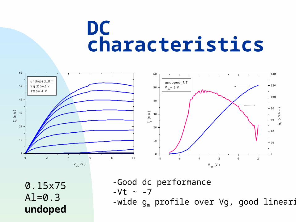
DC characteristics
0 2 4 6 8 100
10
20
30
40
50
60
I d (m
A)
Vds
(V)
undoped_RTVg,top=2 Vstep=-1 V
-8 -6 -4 -2 0 20
10
20
30
40
50
60
I d (m
A)
Vgs
(V)
undoped_RTV
ds= 5 V
0
20
40
60
80
100
120
140
gm (
mS
/mm
)
0.15x75Al=0.3undoped
-Good dc performance-Vt ~ -7-wide gm profile over Vg, good linearity

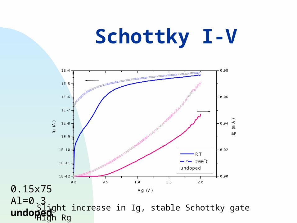
Schottky I-V
-120 -100 -80 -60 -40 -20 0
-0.00005
-0.00004
-0.00003
-0.00002
-0.00001
0.00000
Ig (
A)
Vg (V)
0.15x75 Vbk>100V
0.0 0.5 1.0 1.5 2.01E-12
1E-11
1E-10
1E-9
1E-8
1E-7
1E-6
1E-5
1E-4
Ig (
A)
Vg (V)
undoped
0.00
0.02
0.04
0.06
0.08
0.10
Ig (
mA
)
0.15x75Al=0.3undoped

Small-signal characteristics
1 10 1000
5
10
15
20
25
30
fmax
fT
f T, f
max
(d
B)
frequency (GHz)
fT
fmax
undoped
0.15x75Al=0.3Undoped
Vgs: -3.5Vds: 6

DC characteristics
-12 -10 -8 -6 -4 -2 0 20
10
20
30
40
50
60
70
I d (m
A)
Vgs
(V)
M-dopedVds=4V
0
20
40
60
80
100
120
140
160
180
200
gm (
mS
/mm
)
0.15x75Al=0.3Modulation-doped
0 2 4 6 8 100
10
20
30
40
50
60
70
80
90
ID (
mA
)
VDS (V)
M-dopedVg,top=0.5Vstep=-1.5V
-Good dc performance-Vt ~ -9-narrow gm profile over Vg

Schottky I-V
-120 -100 -80 -60 -40 -20 0
-80
-70
-60
-50
-40
-30
-20
-10
0
10
Ig (A
)
Vg (V)
Vbk:53.4 V
0.0 0.5 1.0 1.5 2.00
5
10
15
20
25
Ig (
mA
)
Vg (V)
RTM-doped
0.15x75Al=0.3Modulation-doped

Small-signal characteristics
1 10 1000
5
10
15
20
25
30
35
fmax
fT
f T, f
ma
x (d
B)
frequency (GHz)
fT
fmax
M-doped
0.15x75Al=0.3M-doped
Vgs: -6Vds: 6

Summary Surface morphology
Step-like structure Surface roughness ~ 0.15 nm, indicating that very smooth surface
and good crystal quality
Electron transport properties For undoped structure, due to the strong spontaneous and
piezoelectric polarization, high 2DEG density obtained, ~1e13 cm-2
Additional doping, modulation doping or channel doping, is not necessary
Device characteristics of AlGaN/GaN HFETs Very large output drain current available, the undoped (~700
mA/mm) and modulation-doped structures (~1000 mA/mm) High breakdown voltage High operation frequency

For microwave high-power devices, the stability of device over temperature is extremely important
The thermal conductivity of substrate Sapphire (0.5 W/cm·K), SiC (4.5 W/cm·K) Self-heating effect
Device structure Undoped structure Modulation-doped structure Channel-doped structure Exhibit different electrical behavior at high temperature
due to their different transport properties
Thermal effect of AlGaN/GaN HFETs

Our work
Compare undoped and modulation-doped AlGaN/GaN HFETs, Al=0.3
Temperature-dependent electron transport properties
Device high temperature performance

Electron transport properties v.s. T
100 200 300 400 5009.00E+012
1.00E+013
1.10E+013
1.20E+013
1.30E+013
1.40E+013
Ele
ctro
n c
on
cen
tra
tion
(cm
-2)
Temperature (K)
Al=0.3 modulation-doped undoped
100 200 300 400 500
500
1000
1500
2000
2500
3000
mo
bili
ty (
cm2 /V
s)
Temperature (K)
Al=0.3 undoped modulation-doped
Thermal activation of Si donors

Charge neutrality condition: give more accurate Ed
n: electron concentration (exp. data, eq (2))NA: acceptor concentration (NA<< ND)ND: donor concentration (ND=5e18)Nc: effective density of state in conduction band (~T3/2)gd: donor spin-degeneracy factor (gd=2)Ed: activation energy (fit parameter)dAlGaN: effective AlGaN thickness (fit parameter)
Calculation of Ed
)exp()(
kT
E
g
N
nNN
nNn d
d
c
AD
A
--- (2)
--- (1) (charge neutrality condition)
AlGaN
ss
d
KNTNn
)100()(

Thermal activation energy
500 400 300 200 1001E14
1E15
1E16
1E17
1E18
n2 /(N
D-n
)
Temperature (K)
fit exp.data
Ed= 83.2 meV

Si donor in GaN, AlGaN Si level in GaN:
Ed~20 meV (for n=1e17 cm-3) Si level in AlGaN:
Al composition and Si doping concentration dependent Si level in Al0.3Ga0.7N
Ed (meV) Growth
1997, MSE-B 110 MBE
1998, SSE 40 MOCVD
2000, PRB 100 MBE
2002, MSE-B 40 MBE
2002, APL 50 Calculation

DC characteristics v.s. T
0 2 4 6 8 100
10
20
30
40
50
60
I d (m
A)
Vds
(V)
undoped RT
200oC
-8 -6 -4 -2 0 20
10
20
30
40
50
I d (m
A)
Vgs
(V)
undoped RT 100oC 200oC
Vds
=5 V
0
20
40
60
80
100
120
140
gm (m
S/m
m)
0.15x75Al=0.3undoped
-Good dc performance from RT to 200°C-Id reduction due to 2DEG mobility degradation-Vt ~ -7, const over temperature, stable gate-wide gm profile over Vg, good linearity
Schottky I-V
0.0 0.5 1.0 1.5 2.01E-12
1E-11
1E-10
1E-9
1E-8
1E-7
1E-6
1E-5
1E-4
Ig (
A)
Vg (V)
RT
200oCundoped
0.00
0.02
0.04
0.06
0.08
Ig (
mA
)
0.15x75Al=0.3undoped
Slight increase in Ig, stable Schottky gateHigh Rg

0 2 4 6 8 100
10
20
30
40
50
60
70
80
I d (m
A)
Vds
(V)
modulation-doped RT
200oC
-10 -8 -6 -4 -2 0 20
10
20
30
40
50
60
70
80
I d (m
A)
VgS
(V)
modulation-doped RT
100oC
200oCV
ds=5 V
0
50
100
150
200
250
gm (
mS
/mm
)
0.15x75Al=0.3Modulation-doped
DC characteristics V.s. T
-Good dc performance from RT to 200°C-Id reduction due to 2DEG mobility degradation-Vt ~ -9, const over temperature, stable gate-narrower gm profile over Vg

Schottky I-V
0.0 0.5 1.0 1.5 2.01E-13
1E-12
1E-11
1E-10
1E-9
1E-8
1E-7
1E-6
1E-5
1E-4
1E-3
0.01
0.1
Ig
(m
A)
Vg (V)
RT
200oCM-doped
0
5
10
15
20
25
Ig
(m
A)
0.15x75Modulation-doped
Slight increase in Ig, stable Schottky gateLower Rg than undoped
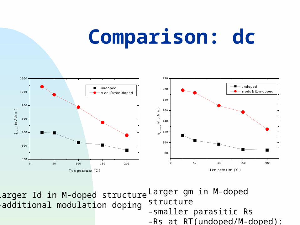
Comparison: dc
0 50 100 150 200500
600
700
800
900
1000
1100
I d, m
ax (
mA
/mm
)
Temperature (oC)
undoped modulation-doped
0 50 100 150 200
80
100
120
140
160
180
200
220
g m, m
ax (
mS
/mm
)
Temperature (oC)
undoped modulation-doped
Larger Id in M-doped structure-additional modulation doping
Larger gm in M-doped structure-smaller parasitic Rs-Rs at RT(undoped/M-doped): 3.4/2.6 Ωmm

Comparison: small-signal
0 50 100 150 20010
20
30
40
50
60
70
80
90
100
f T (
GH
z)
Temperature (oC)
undoped modulation-doped
No obvious degradation observed as T< 100ºC-weak temperature dependence of the electron transport property
higher fT for M-doped - smaller parasitic Rs

Comparison undoped M-doped
Ns constant increase with TMobility comparable at high T for both
Id (T) lower higher
gm (T) lower higher
gm profilewider narrower
Rs (T) higher lower
Rg (T) higher lower
fT (T) lower higher
Modulation-doped structure: better performance over temperatures
Conclusion ICP etching of GaN
Smooth etched surface and vertical sidewall profile obtained
Low resistance Ohmic contacts to n-GaN Plasma-treated Ohmic contacts exhibit low Rc and
excellent thermal stability Even lower Rc obtained using forming gas ambient
Narrow T-gate fabrication 40 nm narrow T-gate was successfully fabricated using
a lower accelerating voltage, 15 kV A specially designed writing pattern
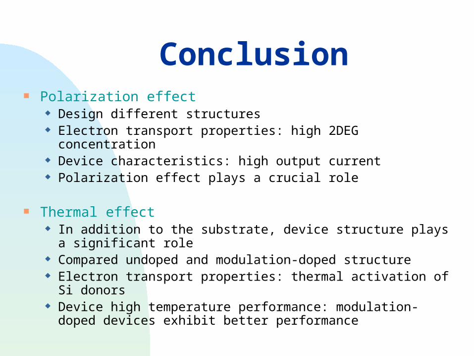
Conclusion Polarization effect
Design different structures Electron transport properties: high 2DEG concentration Device characteristics: high output current Polarization effect plays a crucial role
Thermal effect In addition to the substrate, device structure plays a
significant role Compared undoped and modulation-doped structure Electron transport properties: thermal activation of Si donors Device high temperature performance: modulation-doped
devices exhibit better performance

Comparison: GaN HFETs on sapphire
2DEG Ns
2DEG µ
Lg
(m)
Id, max
(mA/mm)
Gm,ext
(mS/mm)
fT
(GHz)
fmax
(GHz)
2002
EDL
1.3E13
1330
0.18 920 212 101 140
2002
EL
1.2E13
1200
0.25 1400 401 85 151
2001
IEDM
1.2E13
1200
0.15
recess
1310 402 107 148
2001
EL
1.5E13
1170
0.25 1390 216 67 136
Our best
result
1.23E13
953
0.15 1060 200 75 90

Comparison: GaN HFETs on SiC 2DEG Ns
2DEG µ
Lg
(m)
Id, max
(mA/mm)
Gm,ext
(mS/mm)
fT
(GHz)
fmax
(GHz)
2003
EL
1.61E13
993
0.13 1250 250 103 170
2002
EDL
1.1E13
1300
0.12 1230 314 121 162
2001
ED
1.2E13
1200
0.12 1190 217 101 155
2000
EL
1.1E13
1100
0.05 1200 110 140
Our best
result
1.23E13
953
0.15 1060 200 75 90