Tincone Films, a Tin-based Hybrid Material …Annealing of Thin \Tincone" Films, a Tin-based Hybrid...
15
Annealing of Thin “Tincone” Films, a Tin-based Hybrid Material deposited by Molecular Layer Deposition, in Reducing, Inert and Oxidizing Atmospheres Kevin Van de Kerckhove, * Jolien Dendooven, and Christophe Detavernier Department of Solid State Sciences, Ghent University, Krijgslaan 281 S1, 9000 Ghent, Belgium E-mail: [email protected] Abstract Molecular layer deposition (MLD) of hybrid organic-inorganic thin films called ”tincones” is achieved using tetrakisdimethylaminotin (TDMASn) as the metal precursor, and glycerol (GL) as the organic reactant. The GL-based process displays linear growth and self-limiting surface reactions in a broad temperature window ranging from 75 ◦ C to 200 ◦ C. At higher temperatures no film growth is possible. The GPC decreases rapidly with increasing temperature from 1.3 A at 75 ◦ C to less than 0.1 A at 200 ◦ C. The films are observed to be smooth with scanning electron microscopy (SEM) and atomic force microscopy (AFM). The hybrid organic-inorganic nature of the films is visible in both infrared spectroscopy (FTIR) and X-ray photoelectron spectroscopy (XPS). As deposited tincone films are annealed in reducing (H 2 ), inert (He) or oxidizing (O 2 ) atmospheres. In situ X-ray diffraction (XRD) is employed to study the crystallization of the films during annealing. Tincone films annealed in reducing or inert atmosphere crystallize into a tetragonal SnO phase at 388 ◦ C and 410 ◦ C respectively. These temperatures are lower than the crystallization temperature of 480 ◦ C for ALD tin oxide films annealed in H 2 . Tincone films annealed in oxygen crystallize into a SnO 2 phase at a temperature of 523 ◦ C which is similar to the crystallization temperature for ALD tin oxide films annealed in He or O 2 . This reduced temperature for crystallization into SnO for the tincone films is interesting since SnO is one of the few metal oxides known as a p-type semiconductor material. 1
Transcript of Tincone Films, a Tin-based Hybrid Material …Annealing of Thin \Tincone" Films, a Tin-based Hybrid...

Annealing of Thin “Tincone” Films, a Tin-based Hybrid Material
deposited by Molecular Layer Deposition, in Reducing, Inert and
Oxidizing Atmospheres
Kevin Van de Kerckhove,∗ Jolien Dendooven, and Christophe Detavernier
Department of Solid State Sciences, Ghent University, Krijgslaan 281 S1, 9000 Ghent, Belgium
E-mail: [email protected]
Abstract
Molecular layer deposition (MLD) of hybrid organic-inorganic thin films called ”tincones” is achieved using
tetrakisdimethylaminotin (TDMASn) as the metal precursor, and glycerol (GL) as the organic reactant. The
GL-based process displays linear growth and self-limiting surface reactions in a broad temperature window
ranging from 75 ◦C to 200 ◦C. At higher temperatures no film growth is possible. The GPC decreases rapidly
with increasing temperature from 1.3 �A at 75 ◦C to less than 0.1 �A at 200 ◦C. The films are observed to be smooth
with scanning electron microscopy (SEM) and atomic force microscopy (AFM). The hybrid organic-inorganic
nature of the films is visible in both infrared spectroscopy (FTIR) and X-ray photoelectron spectroscopy (XPS).
As deposited tincone films are annealed in reducing (H2), inert (He) or oxidizing (O2) atmospheres. In situ X-ray
diffraction (XRD) is employed to study the crystallization of the films during annealing. Tincone films annealed
in reducing or inert atmosphere crystallize into a tetragonal SnO phase at 388 ◦C and 410 ◦C respectively. These
temperatures are lower than the crystallization temperature of 480 ◦C for ALD tin oxide films annealed in H2.
Tincone films annealed in oxygen crystallize into a SnO2 phase at a temperature of 523 ◦C which is similar to
the crystallization temperature for ALD tin oxide films annealed in He or O2. This reduced temperature for
crystallization into SnO for the tincone films is interesting since SnO is one of the few metal oxides known as a
p-type semiconductor material.
1

Introduction
The current trend towards miniaturization of electronic
devices and components is a driving force for research
into the deposition and properties of thin films. One
thin-film deposition technique that has gained a signif-
icant amount of traction in recent years is atomic layer
deposition (ALD). The ALD technique allows the con-
trolled deposition of nanoscale films of a wide variety of
materials (including metals, metal oxides, sulfides, etc.)
through sequential exposure of the substrate to a pre-
cursor and reactant.1 The self-limiting nature of the gas-
surface reactions allow for sub-nanometer thickness con-
trol and great conformality on 3D structures.
Molecular layer deposition (MLD) is a thin-film depo-
sition technique closely related to ALD. It is employed
for the deposition of purely organic or hybrid organic-
inorganic films. The latter is accomplished by combin-
ing metal-organic precursors, that are usually well-known
from ALD research, with organic reactants such as ethy-
lene glycol (EG) and glycerol (GL). The hybrid films
that are deposited by this technique are commonly re-
ferred to as “metalcones”. An extensive catalog of hybrid
materials has already been established in the literature:
alucone, titanicone, zincone, zircone, hafnicone, vanadi-
cone, and more.2–11 To the extent of our knowledge, no
MLD process for a tin-based metalcone has been reported
yet. Metalcones have been shown to possess several in-
teresting properties in the literature. The organic chains
present in the hybrid films add flexibility to the films,
which is interesting for applications in flexible electronics
and thin-film electrodes.12,13 Post-deposition treatments
are known to transform the metalcone films. Calcination
in air and water etching are able to induce porosity in
alucone films.4,14,15 Annealing of metalcone films in inert
atmosphere leads to a metal oxide/carbon composite film
with improved conductivity.6,11,16,17
Tin oxides have a wide variety of technological applica-
tions. As a semiconductor with a large band-gap, tin
dioxide (SnO2) is a promising material for solid state gas
sensors.18–20 In optical applications, tin oxides are uti-
lized as a transparent conducting oxide in organic light-
emitting diodes (OLED)21,22 and solar cells23,24, and as
surface coatings for functional glasses, due to their re-
flectance in the infrared.25 Tin dioxide is also an inter-
esting, high-capacity, anodic material for lithium-ion bat-
teries.26–28 Tin monoxide (SnO) is one of the few known
p-type semiconductor materials and is hence interesting
for electronic applications such as the fabrication of p-n
junctions and complementary metal oxide semiconductor
(CMOS) architectures.29,30
Many ALD processes are known in the literature for the
deposition of tin oxide films. SnCl4, SnI4 and tetrakis-
dimethylaminotin (TDMASn) are a few common exam-
ples of the Sn metal precursors that are employed in these
processes in combination with water, H2O2, O3 or oxygen
plasma as the reactant. A nice and thorough overview of
tin oxide ALD processes has been written down by Na-
zorov et al.31
In this work, two MLD processes for a novel metalcone
material tincone were investigated. Both processes em-
ploy TDMASn as the tin precursor and ethylene glycol
or glycerol as the organic reactant. The growth of the
tincone films was monitored in situ during the process.
The properties of the grown tincone films were character-
ized with various ex situ methods. A series of as deposited
films was subjected to an annealing treatment in reducing
(H2), inert (He) or oxidizing (O2) atmosphere. The crys-
tallinity of the films was studied during annealing with in
situ X-ray diffraction.
2
Experimental
For the deposition of the tincone films, a custom-built,
pump-type deposition tool was utilized.6 The reactor
walls were kept at a constant temperature of 130 ◦C to
avoid reactant condensation. The container containing
the TDMASn precursor and its delivery line remained
at a temperature of 45 ◦C and 50 ◦C respectively. Argon
(99.999% pure, Air Liquide) was added as a carrier gas
to the TDMASn precursor flow in order to increase the
exposure of substrate to the precursor. The pressure dur-
ing TDMASn exposures was 5 × 10⁻³ mbar. The reactant
bubblers of EG and GL remained at a temperature of re-
spectively 80 ◦C and 60 ◦C. Similarly as for TDMASn,
an additional argon flow was employed during GL expo-
sures. The pressure of EG during the MLD processes
was constant at 2 × 10⁻² mbar. For GL the pressure was
5 × 10⁻³ mbar, including the argon carrier gas flow. In
between exposures or in idle operation, the base pres-
sure of the reactor vessel was in the 10−6 mbar range. Si
with native oxide substrates were used for process devel-
opment, film characterization, and the annealing experi-
ments.
Spectroscopic ellipsometry (SE) was performed with a
model M-2000 ellipsometer J.A. Woollam (300 to 1000
nm). SE measurements provide information on the thick-
ness and optical properties of the hybrid films. The in-
cluded CompleteEASE allowed the analysis of the gath-
ered data. An optical model consisting of a Cauchy dis-
persion relation was sufficient to accurately describe the
SE data. The parameters of the optical model were cal-
ibrated with a series of tincone samples with a known
thickness from X-ray reflectivity measurements (XRR).
The ellipsometer could be mounted on the deposition sys-
tem. Hence, the growth of the tincone films could be
monitored in situ by SE.
The morphology of the tincone films was investigated with
scanning electron microscopy (SEM) and atomic force
microscopy (AFM). SEM imaging was performed on a
Quanta 200F (FEI) microscope using a 10 keV electron
beam. AFM images were acquired on a Bruker Dimension
Edge microscope. The root mean square (rms) roughness
was calculated from the measured 1µm x 1µm AFM im-
ages.
Infrared spectroscopy was carried out on a Vertex 70v
Fourier-transform infrared (FTIR) spectrometer from
Bruker. A globar source (mid IR), DLaTGS detector and
KBr beamsplitter were mounted on the optics bench. The
spectrometer remained under vacuum during measure-
ments to avoid the appearance of atmospheric absorptions
(mainly CO2 and H2O) in the absorption spectra.
X-ray photoelectron spectroscopy (XPS) measurements
were executed on a Thermo Scientific Theta Probe sys-
tem. Aluminium Kα radiation (λ = 0.834 nm) was used
as an excitation source. Analysis of the gathered data
was performed in the CasaXPS software.
XRR and X-ray diffraction (XRD) measurements were
completed on a Bruker D8 Discover diffractometer. For
both XRR and XRD, copper Kα (λ = 0.154 nm) radia-
tion was utilized. During annealing under reducing (He
with 5% H2), inert (He) or oxidizing (He with 5% O2)
atmospheres, in situ XRD was carried out on a home-
built setup fitted with a position-sensitive detector with
a range of 20° in 2θ.32
Results and discussion
In the first section, the process development and char-
acterization is discussed. Secondly, the results of the an-
nealing experiments of tincone films in reducing, inert and
oxidizing atmospheres are presented.
3
20
15
10
5
0
Thickness(nm)
200150100500Cycle number
GLEG
Figure 1: Comparison of the first 200 MLD cycles of the TDMASn/GL and TDMASn/EG processes at a sampletemperature of 100 ◦C.
1.0
0.8
0.6
0.4
0.2
0.0
GPC
(Å)
100806040200Exposure time (s)
TDMASn GL
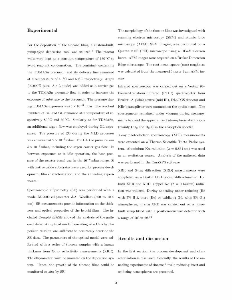
Figure 2: Growth per cycle as a function of precursor and reactant exposure time for the TDMASn/GL MLD processat a sample temperature of 100 ◦C. Saturation is achieved at exposure times of 20 and 60 seconds for TDMASn andGL respectively.
4
1.4
1.2
1.0
0.8
0.6
0.4
0.2
0.0
GPC
(Å)
25020015010050Sample temperature (°C)
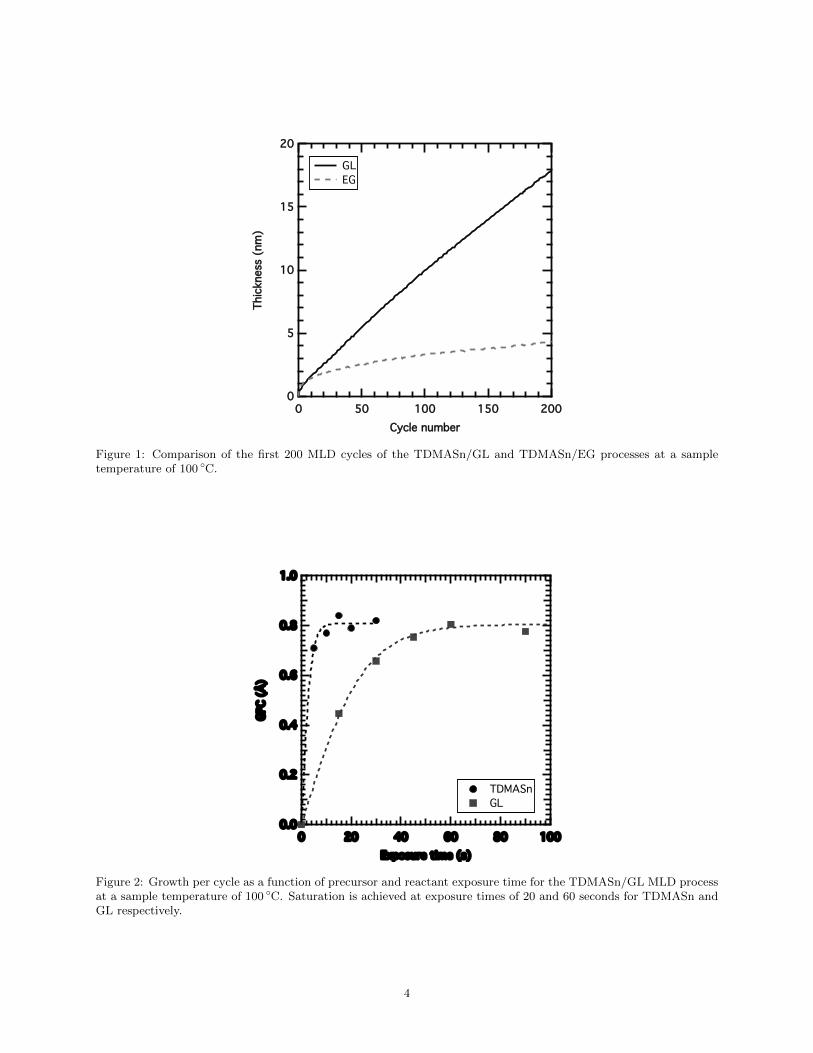
Figure 3: Growth rate versus sample temperature for the TDMASn/GL process. No growth was observed for tem-peratures above 200 ◦C.
The tincone MLD process
Process development
In order to develop a MLD process for a tin-based, hybrid
film, a suitable inorganic precursor and organic reactant
need to be selected. As the inorganic precursor, tetrakis-
dimethylaminotin (TDMASn) is chosen since it is known
as an ALD precursor for the deposition of SnO2.31,33,34
As the organic reactant, ethylene glycol (EG) and glyc-
erol (GL) are tested as they have both been implemented
successfully in multiple MLD processes.2–6,11 By default,
the exposure time for TDMASn is 20 s. For EG and GL,
the standard pulse times are 30 s and 60 s respectively.
In situ ellipsometry enables the monitoring of the film
growth during the TDMASn/EG and TDMASn/GL
MLD processes. After every MLD cycle, the film thick-
ness is measured. The results are presented in figure 1.
There is a clear difference in the growth curves for both
processes. For the TDMASn/GL process, the growth per
cycle (GPC) appears to be stable and the film growth
is linear over 200 cycles. The GPC is 0.8�A at a sample
temperature of 100 ◦C. On the other hand, the GPC of
the TDMASn/EG process decreases dramatically over the
first 50 cycles after which it becomes stable. At a sample
temperature of 100 ◦C, the GPC for the TDMASn/EG
process is 0.1�A after an initial 50 cycles. The decrease in
GPC and slower film growth for an EG-based process in
combination with an alkylamine metal precursor has been
observed before.6,11 The hypothesis is that both OH end
groups of the EG molecules are able to react with surface
groups. These double reactions remove active surface sites
without adding new groups for the TDMASn molecules
to react with. This phenomenon effectively decreases the
growth rate of the hybrid film. Previous investigations
on alucone films have shown that the inherent flexibil-
ity of the organic chains allows these double reactions
to proceed, and that these reactions are detrimental for
the formation of a smooth and closed film. For the TD-
MASn/GL process, these possible double reactions do not
pose a problem for continued film growth since GL pos-
sesses an additional hydroxyl group compared to EG. Due
to its low growth rate, the TDMASn/EG process was not
5

investigated further in this work.
Saturation curves of the GPC were measured to demon-
strate the self-limiting nature of the TDMASn/GL pro-
cess. The saturation curves were measured at sample
temperatures of 100 ◦C (figure 2) and 150 ◦C. At both
temperatures, the GPC saturates at TDMASn and GL
exposure times of respectively 20 s and 60 s.
The temperature window for linear film growth with the
TDMASn/GL process ranges from 75 to 200 ◦C. The
GPC decreases rapidly with increasing temperature and
drops to zero at temperatures above 200 ◦C. The lower
temperature of the temperature window is limited by the
temperature of the hot-wall reactor. At the higher end,
the sample temperature is not limited due to the high
decomposition temperature of TDMASn of 325 ◦C.31 An
increased TDMASn desorption rate at higher tempera-
tures may explain the decrease in GPC.
Characterization of as deposited films
The composition, morphology, and other properties of as
deposited tincone films were studied ex situ. The tin-
cone films are grown with 300 cycles of the TDMASn/GL
process at a substrate temperature of 100 ◦C on a silicon
substrate with native oxide. All tincone samples used for
characterization or annealing experiments were freshly de-
posited in order to avoid any effect of aging in atmospheric
conditions. Although, in the course of a week, no changes
in density or composition of the films was observed during
aging.
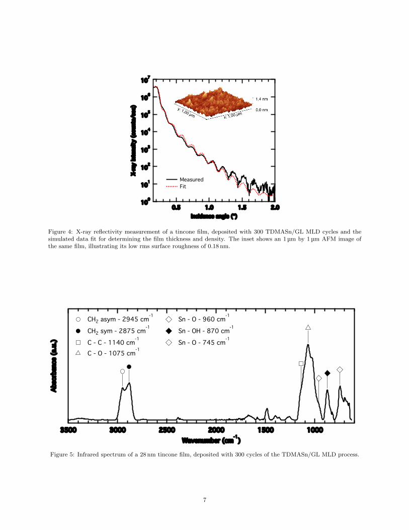
As deposited, the thickness of the films is 28.3 nm and the
density is 2.5 g/cm3. These values were derived from a
simulation of the XRR pattern that is in good agreement
with the measurement data (figure 4). The surface mor-
phology of the film was verified with AFM. A measure-
ment of an as deposited film is presented in the inset of
figure 4 and shows that the films have a low surface rough-
ness. SEM confirms this statement on the nanoscopic
level as shown in figure 8.
A working optical model for analyzing the in situ ellip-
sometry data was constructed for the hybrid tincone films.
A model consisting of a simple Cauchy dispersion relation
of the type n(λ) = A+B/λ2 +C/λ4 was sufficient for ac-
quiring a good fit for the SE data. A series of tincone film
thickness measurements by XRR were employed to cali-
brate the parameters of the optical model. This calibra-
tion procedure yielded the following parameter values: A
= 1.408, B = 1.725 × 10⁴ nm2 and C = −4.29 × 10⁸ nm4.
At a wavelength of 600 nm, the calculated refractive index
is 1.45 in this model.
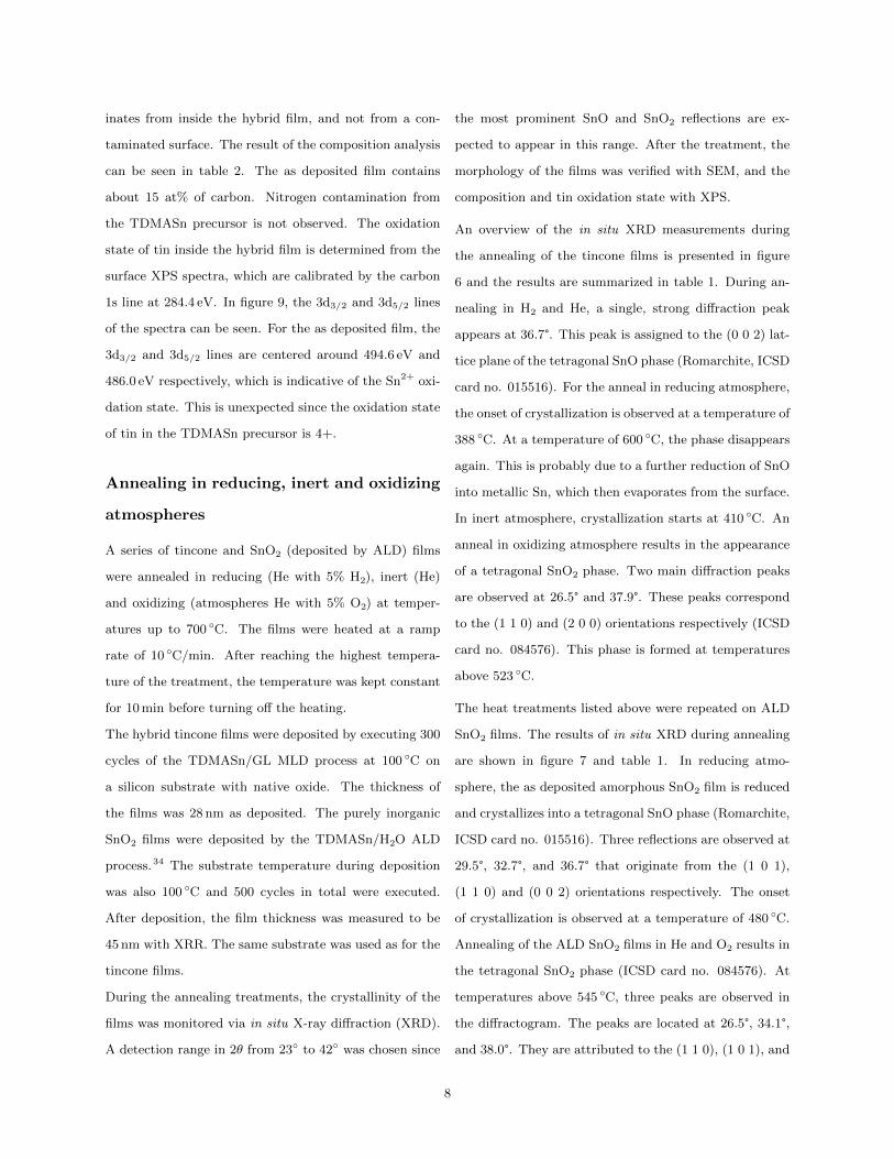
Fourier transform infrared spectroscopy (FTIR) was per-
formed on as deposited tincone films in order to inves-
tigate the chemical composition of the films. The films
were measured ex situ. The result of the measurement
is shown in figure 5. Two absorption peaks are visible at
2945 cm−1 and 2875 cm−1. These peaks are related to the
asymmetrical and symmetrical CH2 stretch modes respec-
tively. The “fingerprint” region of the spectrum reveals
the CH2 twisting, and C-C and C-O stretching modes
at wavenumbers of 1252 cm−1, 1140 cm−1 and 1075 cm−1
respectively.2 At lower wavenumbers several tin-related
modes appear in the spectrum. The peaks at 960 cm−1
and 745 cm−1 originate from Sn-O stretching vibrations.
The absorption at 870 cm−1 has been previously assigned
to vibrations of Sn-OH bonds.35–37 The presence of both
inorganic and organic components in the spectrum are
indicative of the hybrid nature of the film.
X-ray photoelectron spectroscopy (XPS) was also em-
ployed to verify the composition of the films, and the ox-
idation state of Sn inside the films. For determining the
atomic composition of the films, first carbon contamina-
tion of the surface was removed with two argon sputtering
steps. This ensures that the measured carbon signal orig-
6
100
101
102
103
104
105
106
107
X-ra
y in
tens
ity (
coun
ts/s
ec)
2.01.51.00.5Incidence angle (°)
Measured Fit
Figure 4: X-ray reflectivity measurement of a tincone film, deposited with 300 TDMASn/GL MLD cycles and thesimulated data fit for determining the film thickness and density. The inset shows an 1µm by 1 µm AFM image ofthe same film, illustrating its low rms surface roughness of 0.18 nm.
Abso
rban
ce (
a.u.
)
3500 3000 2500 2000 1500 1000Wavenumber (cm-1)
CH2 asym - 2945 cm-1 Sn - O - 960 cm-1
CH2 sym - 2875 cm-1 Sn - OH - 870 cm-1
C - C - 1140 cm-1 Sn - O - 745 cm-1
C - O - 1075 cm-1
Figure 5: Infrared spectrum of a 28 nm tincone film, deposited with 300 cycles of the TDMASn/GL MLD process.
7
inates from inside the hybrid film, and not from a con-
taminated surface. The result of the composition analysis
can be seen in table 2. The as deposited film contains
about 15 at% of carbon. Nitrogen contamination from
the TDMASn precursor is not observed. The oxidation
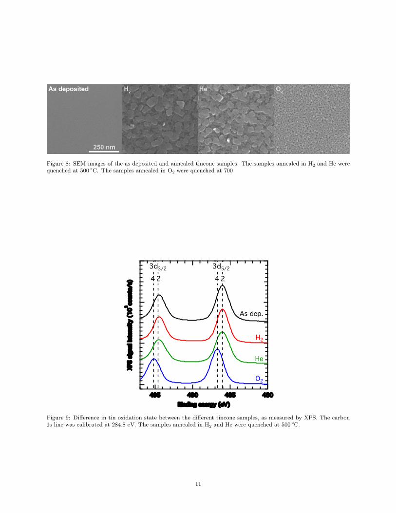
state of tin inside the hybrid film is determined from the
surface XPS spectra, which are calibrated by the carbon
1s line at 284.4 eV. In figure 9, the 3d3/2 and 3d5/2 lines
of the spectra can be seen. For the as deposited film, the
3d3/2 and 3d5/2 lines are centered around 494.6 eV and
486.0 eV respectively, which is indicative of the Sn2+ oxi-
dation state. This is unexpected since the oxidation state
of tin in the TDMASn precursor is 4+.
Annealing in reducing, inert and oxidizing
atmospheres
A series of tincone and SnO2 (deposited by ALD) films
were annealed in reducing (He with 5% H2), inert (He)
and oxidizing (atmospheres He with 5% O2) at temper-
atures up to 700 ◦C. The films were heated at a ramp
rate of 10 ◦C/min. After reaching the highest tempera-
ture of the treatment, the temperature was kept constant
for 10 min before turning off the heating.
The hybrid tincone films were deposited by executing 300
cycles of the TDMASn/GL MLD process at 100 ◦C on
a silicon substrate with native oxide. The thickness of
the films was 28 nm as deposited. The purely inorganic
SnO2 films were deposited by the TDMASn/H2O ALD
process.34 The substrate temperature during deposition
was also 100 ◦C and 500 cycles in total were executed.
After deposition, the film thickness was measured to be
45 nm with XRR. The same substrate was used as for the
tincone films.
During the annealing treatments, the crystallinity of the
films was monitored via in situ X-ray diffraction (XRD).
A detection range in 2θ from 23◦ to 42◦ was chosen since
the most prominent SnO and SnO2 reflections are ex-
pected to appear in this range. After the treatment, the
morphology of the films was verified with SEM, and the
composition and tin oxidation state with XPS.
An overview of the in situ XRD measurements during
the annealing of the tincone films is presented in figure
6 and the results are summarized in table 1. During an-
nealing in H2 and He, a single, strong diffraction peak
appears at 36.7°. This peak is assigned to the (0 0 2) lat-
tice plane of the tetragonal SnO phase (Romarchite, ICSD
card no. 015516). For the anneal in reducing atmosphere,
the onset of crystallization is observed at a temperature of
388 ◦C. At a temperature of 600 ◦C, the phase disappears
again. This is probably due to a further reduction of SnO
into metallic Sn, which then evaporates from the surface.
In inert atmosphere, crystallization starts at 410 ◦C. An
anneal in oxidizing atmosphere results in the appearance
of a tetragonal SnO2 phase. Two main diffraction peaks
are observed at 26.5° and 37.9°. These peaks correspond
to the (1 1 0) and (2 0 0) orientations respectively (ICSD
card no. 084576). This phase is formed at temperatures
above 523 ◦C.
The heat treatments listed above were repeated on ALD
SnO2 films. The results of in situ XRD during annealing
are shown in figure 7 and table 1. In reducing atmo-
sphere, the as deposited amorphous SnO2 film is reduced
and crystallizes into a tetragonal SnO phase (Romarchite,
ICSD card no. 015516). Three reflections are observed at
29.5°, 32.7°, and 36.7° that originate from the (1 0 1),
(1 1 0) and (0 0 2) orientations respectively. The onset
of crystallization is observed at a temperature of 480 ◦C.
Annealing of the ALD SnO2 films in He and O2 results in
the tetragonal SnO2 phase (ICSD card no. 084576). At
temperatures above 545 ◦C, three peaks are observed in
the diffractogram. The peaks are located at 26.5°, 34.1°,
and 38.0°. They are attributed to the (1 1 0), (1 0 1), and
8

6004002000Temperature (°C)
SnO2
40
35
30
25
2 Th
eta
(°)
6004002000Temperature (°C)
SnO
6004002000Temperature (°C)
SnOHeH2 O2
Figure 6: In situ XRD measurements during annealing of tincone films, deposited with 300 MLD cycles, in reducing(H2), inert (He), and oxidizing (O2) atmospheres. The films were heated at a rate of 10 ◦C/min to 700 ◦C, 500 ◦C,and 700 ◦C in each atmosphere respectively.
6004002000Temperature (°C)
SnO2
40
35
30
25
2 Th
eta
(°)
6004002000Temperature (°C)
SnO
6004002000Temperature (°C)
SnO2
HeH2 O2
Figure 7: In situ XRD measurements during annealing of reference SnO2 films of 45 nm, deposited by the TD-MASn/H2O, in reducing (H2), inert (He), and oxidizing (O2) atmospheres. The films were heated at a rate of10 ◦C/min to 500 ◦C, 700 ◦C and 700 ◦C in each atmosphere respectively.
Table 1: Overview table of the formation temperatures (top) and phases (bottom) during annealing of as depositedMLD tincone and ALD SnO2 in reducing (H2), inert (He), and oxidizing (O2) atmospheres.
H2 He O2
Tincone 388 ◦C 410 ◦C 523 ◦C
SnO (tetragonal) SnO (tetragonal) SnO2 (tetragonal)
ALD SnO2 480 ◦C 545 ◦C 545 ◦C
SnO (tetragonal) SnO2 (tetragonal) SnO2 (tetragonal)
9
(2 0 0) lattice planes respectively.
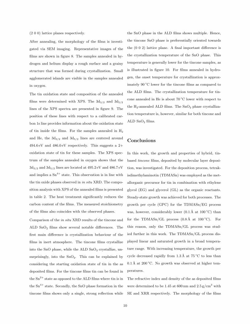
After annealing, the morphology of the films is investi-
gated via SEM imaging. Representative images of the
films are shown in figure 8. The samples annealed in hy-
drogen and helium display a rough surface and a grainy
structure that was formed during crystallization. Small
agglomerated islands are visible in the samples annealed
in oxygen.
The tin oxidation state and composition of the annealed
films were determined with XPS. The 3d3/2 and 3d5/2
lines of the XPS spectra are presented in figure 9. The
position of these lines with respect to a calibrated car-
bon 1s line provides information about the oxidation state
of tin inside the films. For the samples annealed in H2
and He, the 3d3/2 and 3d5/2 lines are centered around
494.6 eV and 486.0 eV respectively. This suggests a 2+
oxidation state of tin for these samples. The XPS spec-
trum of the samples annealed in oxygen shows that the
3d3/2 and 3d5/2 lines are located at 495.2 eV and 486.7 eV
and implies a Sn4+ state. This observation is in line with
the tin oxide phases observed in in situ XRD. The compo-
sition analysis with XPS of the annealed films is presented
in table 2. The heat treatment significantly reduces the
carbon content of the films. The measured stoichiometry
of the films also coincides with the observed phases.
Comparison of the in situ XRD results of the tincone and
ALD SnO2 films show several notable differences. The
first main difference is crystallization behaviour of the
films in inert atmosphere. The tincone films crystallize
into the SnO phase, while the ALD SnO2 crystallize, un-
surprisingly, into the SnO2. This can be explained by
considering the starting oxidation state of tin in the as
deposited films. For the tincone films tin can be found in
the Sn2+ state as opposed to the ALD films where tin is in
the Sn4+ state. Secondly, the SnO phase formation in the
tincone films shows only a single, strong reflection while
the SnO phase in the ALD films shows multiple. Hence,
the tincone SnO phase is preferentially oriented towards
the (0 0 2) lattice plane. A final important difference is
the crystallization temperature of the SnO phase. This
temperature is generally lower for the tincone samples, as
is illustrated in figure 10. For films annealed in hydro-
gen, the onset temperature for crystallization is approx-
imately 90 ◦C lower for the tincone films as compared to
the ALD films. The crystallization temperature for tin-
cone annealed in He is about 70 ◦C lower with respect to
the H2-annealed ALD films. The SnO2 phase crystalliza-
tion temperature is, however, similar for both tincone and
ALD SnO2 films.
Conclusions
In this work, the growth and properties of hybrid, tin-
based tincone films, deposited by molecular layer deposi-
tion, was investigated. For the deposition process, tetrak-
isdimethylaminotin (TDMASn) was employed as the met-
allorganic precursor for tin in combination with ethylene
glycol (EG) and glycerol (GL) as the organic reactants.
Steady-state growth was achieved for both processes. The
growth per cycle (GPC) for the TDMASn/EG process
was, however, considerably lower (0.1�A at 100 ◦C) than
for the TDMASn/GL process (0.8�A at 100 ◦C). For
this reason, only the TDMASn/GL process was stud-
ied further in this work. The TDMASn/GL process dis-
played linear and saturated growth in a broad tempera-
ture range. With increasing temperature, the growth per
cycle decreased rapidly from 1.3�A at 75 ◦C to less than
0.1�A at 200 ◦C. No growth was observed at higher tem-
peratures.
The refractive index and density of the as deposited films
were determined to be 1.45 at 600 nm and 2.5 g/cm3 with
SE and XRR respectively. The morphology of the films
10
As deposited H2 O2
250 nm
He
Figure 8: SEM images of the as deposited and annealed tincone samples. The samples annealed in H2 and He werequenched at 500 ◦C. The samples annealed in O2 were quenched at 700
XPS
signa
l int
ensit
y (1
03 coun
ts/s
)
495 490 485 480Binding energy (eV)
As dep.
H2
O2
He
3d5/2
4 23d3/2
4 2
Figure 9: Difference in tin oxidation state between the different tincone samples, as measured by XPS. The carbon1s line was calibrated at 284.8 eV. The samples annealed in H2 and He were quenched at 500 ◦C.
11

Table 2: Summary of the characterization results of the as deposited and annealed tincone films. The samplesannealed in H2 and He were quenched at 500 ◦C.
Crystallinity Composition (at%)
C Sn O
As deposited Amorphous 15 52 33
Anneal in He to 500 ◦C SnO 5 52 43
Anneal in H2 to 500 ◦C SnO 7 53 40
Anneal in O2 to 700 ◦C SnO2 1 38 61
1000
800
600
400
200
0
XRD
inte
nsity
(co
unts
/sec
)
6005004003002001000Temperature (°C)
Tincone - He Tincone - H2 SnO2 - H2
Figure 10: XRD intensity of the (2 0 0) SnO reflection as a function of temperature. The (2 0 0) reflection correspondsto a 2θ value of 36.7 degrees.
was shown to be smooth with a low surface roughness
with SEM and AFM. The hybrid nature of the as de-
posited films was confirmed with both FTIR and XPS.
Both spectra displayed both organic and inorganic com-
ponents. XPS revealed the oxidation state of tin in the
as deposited films to be 2+.
As deposited tincone films were annealed in reducing
(H2), inert (He) or oxidizing (O2) atmospheres. The crys-
tallization of the films was studied in situ with X-ray
diffraction (XRD). Ex situ the annealed films were stud-
ied with SEM and XPS. For comparison purposes, tin
oxide films deposited via ALD were subjected to identi-
cal annealing treatments. XRD revealed that both the
films annealed in reducing or inert atmospheres crystal-
lized to a tetragonal tin monoxide phase at 388 ◦C and
410 ◦C respectively. This was supported by XPS mea-
surements that indicated a 2+ oxidation state for tin. In
comparison, the ALD tin oxide films crystallized into SnO
only in reducing atmosphere and at a higher temperature
of 480 ◦C. The tincone films that crystallized into SnO
during annealing displayed a grainy and rough structure
in SEM, and a significantly reduced carbon content in
XPS. The tincone films annealed in oxygen crystallized
into a tetragonal SnO2 phase at 523 ◦C. This observation
was also supported by a tin oxidation state of 4+ seen in
XPS. Similar crystallization behaviour was observed for
12

the reference ALD tin oxide films that were annealed in
inert or oxidizing atmosphere. Tincone films annealed in
oxygen showed small agglomerated islands in SEM. XPS
indicated that all carbon content was removed from these
films during the annealing treatment.
This work adds a new hybrid ”metalcone” to the catalog
of materials that can be deposited via MLD. The results
from the annealing experiments may prove to be inter-
esting for the semiconductor industry since SnO is one of
the few metal oxides known as a p-type semiconductor
material.
Acknowledgement
The authors are grateful to FWO Vlaanderen for pro-
viding Kevin Van de Kerckhove with financial support
through the mandate of Aspirant. J.D. acknowledges
the FWO for a post-doc grant. They also acknowledge
the IWT Vlaanderen (IWT-SBO SOSLion project), BOF-
UGent (GOA 01G01513), and the Hercules foundation for
providing funding for this work. They thank Karl Op-
somer and Matthias Minjauw for the XPS measurements,
Tareq Ahmad for AFM, and Olivier Janssens for SEM
work.
References
(1) George, S. M. Chemical Reviews 2010, 110, 111–
131.
(2) Bertrand, J. A.; Dameron, A. A.; Seghete, D.;
Burton, B. B.; Davidson, S. D.; Cavanagh, A. S.;
George, S. M. Chemistry of Materials 2008, 20,
3315–3326.
(3) George, S. M.; Lee, B. H.; Yoon, B.; Abdulaga-
tov, A. I.; Hall, R. A. Journal of Nanoscience and
Nanotechnology 2011, 11, 7948–7955.
(4) Van de Kerckhove, K.; Barr, M. K. S.; Santi-
nacci, L.; Vereecken, P. M.; Dendooven, J.; Detav-
ernier, C. Dalton Transactions 2018,
(5) Abdulagatov, A. I.; Hall, R. A.; Sutherland, J. L.;
Lee, B. H.; Cavanagh, A. S.; George, S. M. Chem-
istry of Materials 2012, 24, 2854–2863.
(6) Van de Kerckhove, K.; Mattelaer, F.; De-
duytsche, D.; Vereecken, P. M.; Dendooven, J.; De-
tavernier, C. Dalton Transactions 2016, 45, 1176–
1184.
(7) Yoon, B.; O’Patchen, J. L.; Seghete, D.; Ca-
vanagh, A. S.; George, S. M. Chemical Vapor De-
position 2009, 15, 112–121.
(8) Peng, Q.; Gong, B.; VanGundy, R. M.; Par-
sons, G. N. Chemistry of Materials 2009, 21, 820–
830.
(9) Lee, B. H.; Anderson, V. R.; George, S. M. Chemical
Vapor Deposition 2013, 19, 204–212.
(10) Lee, B. H.; Anderson, V. R.; George, S. M. ACS Ap-
plied Materials & Interfaces 2014, 6, 16880–16887.
(11) Van de Kerckhove, K.; Mattelaer, F.; Dendooven, J.;
Detavernier, C. Dalton Transactions 2017, 192,
1126–20.
(12) Lee, B. H.; Lee, K. H.; Im, S.; Sung, M. M. Organic
Electronics 2008, 9, 1146–1153.
(13) Lee, B. H.; Yoon, B.; Anderson, V. R.; George, S. M.
The Journal of Physical Chemistry C 2012, 116,
3250–3257.
(14) Liang, X.; Yu, M.; Li, J.; Jiang, Y.-B.;
Weimer, A. W. Chemical Communications 2009,
7140–7142.
13
(15) Liang, X.; Evanko, B. W.; Izar, A.; King, D. M.;
Jiang, Y.-B.; Weimer, A. W. Microporous and Meso-
porous Materials 2013, 168, 178–182.
(16) DuMont, J. W.; George, S. M. Journal of Physical
Chemistry C 2015, 119, 14603–14612.
(17) Abdulagatov, A. I.; Terauds, K. E.; Travis, J. J.;
Cavanagh, A. S.; Raj, R.; George, S. M. Journal of
Physical Chemistry C 2013, 117, 17442–17450.
(18) Rumyantseva, M. N.; Safonova, O. V.;
Boulova, M. N.; Ryabova, L. I.; Gas’kov, A. M.
Russian Chemical Bulletin 2003, 52, 1217–1238.
(19) Arafat, M. M.; Dinan, B.; Akbar, S. A.; Haseeb, A.
S. M. A. Sensors 2012, 12, 7207–7258.
(20) Choi, G.; Satyanarayana, L.; Park, J. Applied Sur-
face Science 2006, 252, 7878–7883.
(21) Tan, S.-S.; Kee, Y.-Y.; Wong, H.-Y.; Tou, T.-Y. Sur-
face & Coatings Technology 2013, 231, 98–101.
(22) Gorrn, P.; Ghaffari, F.; Riedl, T.; Kowalsky, W.
Solid State Electronics 2009, 53, 329–331.
(23) Chou, L.-W.; Lin, Y.-Y.; Wu, A. T. Applied Surface
Science 2013, 277, 30–34.
(24) Kang, B.; Tan, L. W.; Silva, S. R. P. Applied Physics
Letters 2008, 93, 133302–3.
(25) Gordon, R. Journal of Non-Crystalline Solids 1997,
218, 81–91.
(26) Idota, Y. Science 1997, 276, 1395–1397.
(27) Mohamedi, M.; Lee, S. J.; Takahashi, D.;
Nishizawa, M.; Itoh, T.; Uchida, I. Electrochimica
Acta 2001, 46, 1161–1168.
(28) Meduri, P.; Pendyala, C.; Kumar, V.; Sumanasek-
era, G. U.; Sunkara, M. K. Nano Letters 2009, 9,
612–616.
(29) Caraveo-Frescas, J. A.; Nayak, P. K.; Al-
Jawhari, H. A.; Granato, D. B.; Schwingen-
schlogl, U.; Alshareef, H. N. ACS Nano 2013, 7,
5160–5167.
(30) Han, J. H.; Chung, Y. J.; Park, B. K.; Kim, S. K.;
Kim, H.-S.; Kim, C. G.; Chung, T.-M. Chemistry of
Materials 2014, 26, 6088–6091.
(31) Nazarov, D. V.; Bobrysheva, N. P.; Os-
molovskaya, O. M.; Osmolovsky, M. G.;
Smirnov, V. M. Reviews on Advanced Materi-
als Science 2015, 40, 262–275.
(32) Knaepen, W.; Detavernier, C.;
Van Meirhaeghe, R. L.; Jordan Sweet, J.; Lavoie, C.
Thin Solid Films 2008, 516, 4946–4952.
(33) Elam, J. W.; Baker, D. A.; Hryn, A. J.; Martin-
son, A. B. F.; Pellin, M. J.; Hupp, J. T. Journal of
Vacuum Science & Technology A 2008, 26, 244–252.
(34) Mullings, M. N.; Hagglund, C.; Bent, S. F. Jour-
nal of Vacuum Science & Technology A 2013, 31,
061503–9.
(35) Chaisitsak, S. Sensors 2011, 11, 7127–7140.
(36) Van Tran, T.; Turrell, S.; Eddafi, M.; Capoen, B.;
Bouazaoui, M.; Roussel, P.; Berneschi, S.; Righ-
ini, G.; Ferrari, M.; Bhaktha, S. N. B.; Cristini, O.;
Kinowski, C. Journal of Molecular Structure 2010,
976, 314–319.
(37) Khan, A. F.; Mehmood, M.; Aslam, M.; Ashraf, M.
Applied Surface Science 2010, 256, 2252–2258.
14

Graphical TOC Entry
15


![Redalyc.Corrosion resistance of hybrid films applied on … impacts compared to the chromatization process [2]. Moreover, siloxane-PMMA hybrid films promote an excellent anchorage](https://static.fdocuments.in/doc/165x107/5af46b5f7f8b9a5b1e8c7534/resistance-of-hybrid-films-applied-on-impacts-compared-to-the-chromatization.jpg)