Timing Measurement Problems and Solutions in Source ...
25
DesignCon 2010 Timing Measurement Problems and Solutions in Source Terminated Memory Systems with Inaccessible Probing Points John Kenney, Juniper Networks [email protected] Peter J. Pupalaikis, LeCroy Corporation [email protected]
Transcript of Timing Measurement Problems and Solutions in Source ...

DesignCon 2010
Timing Measurement Problems and Solutions in Source Terminated Memory Systems with Inaccessible Probing Points
John Kenney, Juniper Networks [email protected] Peter J. Pupalaikis, LeCroy Corporation [email protected]

Abstract This paper discusses the common problem of making setup and hold measurements in memory systems where the desired probing point is inaccessible. Timing measurement problems of this type are problematic not only in skew due to incorrect probing locations, but also due to waveform distortions due to reflections created by various termination schemes. The paper considers various problems specifically in termination methods utilized in memory systems and offers some solutions and methods for mitigating measurement problems. A real-life example in a QDR memory system is used.
Author(s) Biography John Kenney was born in West Hartford, Connecticut in 1965. He received a B.A. degree from Stonehill College in 1987, a B.S. degree in electrical engineering from the University of Notre Dame in 1988, and a M.S. in electrical engineering from the California Institute of Technology in 1992.
John has worked in the Networking Industry over 15 years. He joined Juniper Networks in 2001, thru the acquisition of Unisphere Networks. He has been a designer and architect for the Juniper E-series of routers since 1997. He is currently a lead engineer and architect.
Pete Pupalaikis was born in Boston, Massachusetts in 1964 and received the B.S. degree in electrical engineering from Rutgers University, New Brunswick, New Jersey in 1988.
He has worked at LeCroy Corporation for 15 years and is currently Vice President and Principal Technologist. He holds over twenty patents in the area of measurement instrument design and is a member of Tau Beta Pi, Eta Kappa Nu and the IEEE signal processing, instrumentation, and microwave societies.

1
Introduction As systems become more integrated and system frequencies/edge-rates increase, it becomes necessary to pack more components in closer proximity, in an effort to reduce etch lengths and stubbing effects. This packing of components often results in reduced visibility of signal end-points. This paper describes an example of such a scenario, a method for virtually-probing an inaccessible endpoint, a method for correlating the approach, and the theory behind the results obtained. It is a rare example of top-to-bottom closure in the analysis of a real-world problem. Although the circuit analyzed is relatively low-frequency, by today’s standards, the principals discussed can be applied to many other situations where virtual probing is required.
The System The circuit under investigation resides on a production line-card – a routing blade in an edge router. The circuit assembly is complex – roughly 15” square with over 6200 components, routed using a 28 layer PCB. Real-estate is at a premium, with components placed on both top and bottom of the card. A combination of ASIC, FPGA, and off-the-shelf processor technology is used to process IP packets at line-rate. The problem at hand was experienced on a memory interface of an off-the-shelf Network Processing Unit (NPU). A NPU is a processor geared towards the processing of packets – equipped with streaming interfaces, buffering, scheduling and internal micro-engines implementing code sets tailored towards the operations typically performed on a packet. Like many processors, the NPU uses external memory for code store, packet buffering, and databases. DRAM is used for buffering where density and speed are important and latency can be tolerated. SRAM is used for databases, where low latency is important and density is not as important.
The problem The problem observed was that under certain environmental and traffic conditions, parity errors were experienced on a particular NPU memory interface. The interface was a database interface implemented using a QDRII memory. Thru post-failure analysis, it was determined that the error was in the write path, and the failing bit was the parity bit itself. To gain a full understanding of the problem, it was important to observe the appropriate signals at the time of the failure to answer the following questions: What was the failure – a setup time violation, a hold time violation, etc.? What was the cause of the failure – clock jitter, poor signal quality, power glitch, excessive loading, etc.?
Block diagram A block diagram of the memory subsystem is shown below. The NPU has a dedicated QDRII/LA1 interface running at 214MHz. There are two target components on the interface – a QDRII memory and a Content Addressable Memory (CAM). For signal integrity, the devices are clam-shelled to minimize stubbing. (The CAM has a footprint with a mirror image of a QDR memory footprint in one quadrant, to allow a QDR memory to be clamshelled on the back.) Using this technique, pin-escape vias can be shared between top and bottom component signals,
QDR and QDRII are trademarks of the QDR consortium

2
minimizing stub lengths. As we will see, for most signals this is effective. For several, stubbing cannot be avoided.
Figure 1 - Memory sub-system block diagram
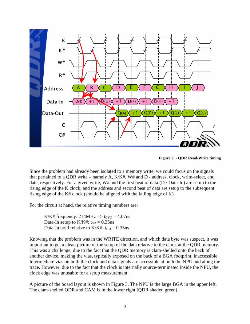
QDR protocol QDR memory is Quad Data Rate – Data is written on two edges of a write clock while data is read on two edges of a read clock – four clock edges are used per clock period. Data is written from the NPU to the memory using the D[17:0] bus and the K/K# clock. Data is read over the Q[17:0] bus using the C/C# clock. The two components are distinguished on the bus using the W# (writes) and R# (reads) signals. The QDR standard describes burst-of-two and burst-of-four memories. The memories used for this design are burst-of-two. For a given address, two beats of data are written into or read out of the memory. The memory is logically a 32-bit (36 with parity) memory, implemented using a 2-beat 16-bit bus. A functional timing diagram of the QDRII standard1 is shown in Figure 2 for reference.
3
Figure 2 - QDR Read/Write timing
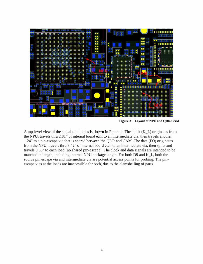
Since the problem had already been isolated to a memory write, we could focus on the signals that pertained to a QDR write – namely A, K/K#, W# and D - address, clock, write-select, and data, respectively. For a given write, W# and the first beat of data (D / Data-In) are setup to the rising edge of the K clock, and the address and second beat of data are setup to the subsequent rising edge of the K# clock (should be aligned with the falling edge of K). For the circuit at hand, the relative timing numbers are: K/K# frequency: 214MHz => tCYC = 4.67ns Data-In setup to K/K#: tSD = 0.35ns Data-In hold relative to K/K#: tHD = 0.35ns Knowing that the problem was in the WRITE direction, and which data byte was suspect, it was important to get a clean picture of the setup of the data relative to the clock at the QDR memory. This was a challenge, due to the fact that the QDR memory is clam-shelled onto the back of another device, making the vias, typically exposed on the back of a BGA footprint, inaccessible. Intermediate vias on both the clock and data signals are accessible at both the NPU and along the trace. However, due to the fact that the clock is internally source-terminated inside the NPU, the clock edge was unusable for a setup measurement. A picture of the board layout is shown in Figure 3. The NPU is the large BGA in the upper left. The clam-shelled QDR and CAM is in the lower right (QDR shaded green).
4
Figure 3 - Layout of NPU and QDR/CAM
A top-level view of the signal topologies is shown in Figure 4. The clock (K_L) originates from the NPU, travels thru 2.81” of internal board etch to an intermediate via, then travels another 1.24” to a pin-escape via that is shared between the QDR and CAM. The data (D9) originates from the NPU, travels thru 3.42” of internal board etch to an intermediate via, then splits and travels 0.53” to each load (no shared pin-escape). The clock and data signals are intended to be matched in length, including internal NPU package length. For both D9 and K_L, both the source pin escape via and intermediate via are potential access points for probing. The pin-escape vias at the loads are inaccessible for both, due to the clamshelling of parts.

5
Figure 4 - Data and clock etch topologies
A cross-sectional view is shown in Figure 5, indicating where the signals were, in fact, probed. Again, D9 is shown in blue and K_L is shown in red. The turquoise etch, via, and ball are the leg of the D9 signal which go to the CAM.
Figure 5 - Board cross-section

6
The frequency of the clock signal was 214MHz and the 20-80% rise-time was about 500ps. The 6GHz/20GSps scope used had sufficient bandwidth to capture all of the salient features of the waveforms. In reality, for the purposes of this experiment, the most important thing for us was to observe a monotonic clock edge, about which to measure setup time. With this, triggers of setup time violations could later be created.
Direct Probing Due to the fact that the signals were being probed mid-way between the driver and receiver, the plan was to measure the distance between the rising edge of the clock and either edge of the data and adjust, based on the relationship of probing via to end-point. For example, the clock signal is probed 1.24” from the endpoint, and the data is probed 0.5” from the endpoint. This is a difference of 0.74” of etch length. Assuming ~175 ps per inch for FR4, this would be a difference of ~130ps. Instead of a 350ps setup requirement, we would change to a 220ps setup time, as measured at the intermediate vias. A picture of the setup is shown in Figure 6.
Figure 6 - Picture of board probing setup
Unfortunately, probing a source terminated clock (K_L) at an intermediate point in the transmission line produces the waveform shown in Figure 7. The K_L clock is shown in blue. Note that the signal is non-monotonic – a signal that is very hard to make a setup measurement against.

7
Figure 7 – Clock and data waveform acquired at probing point
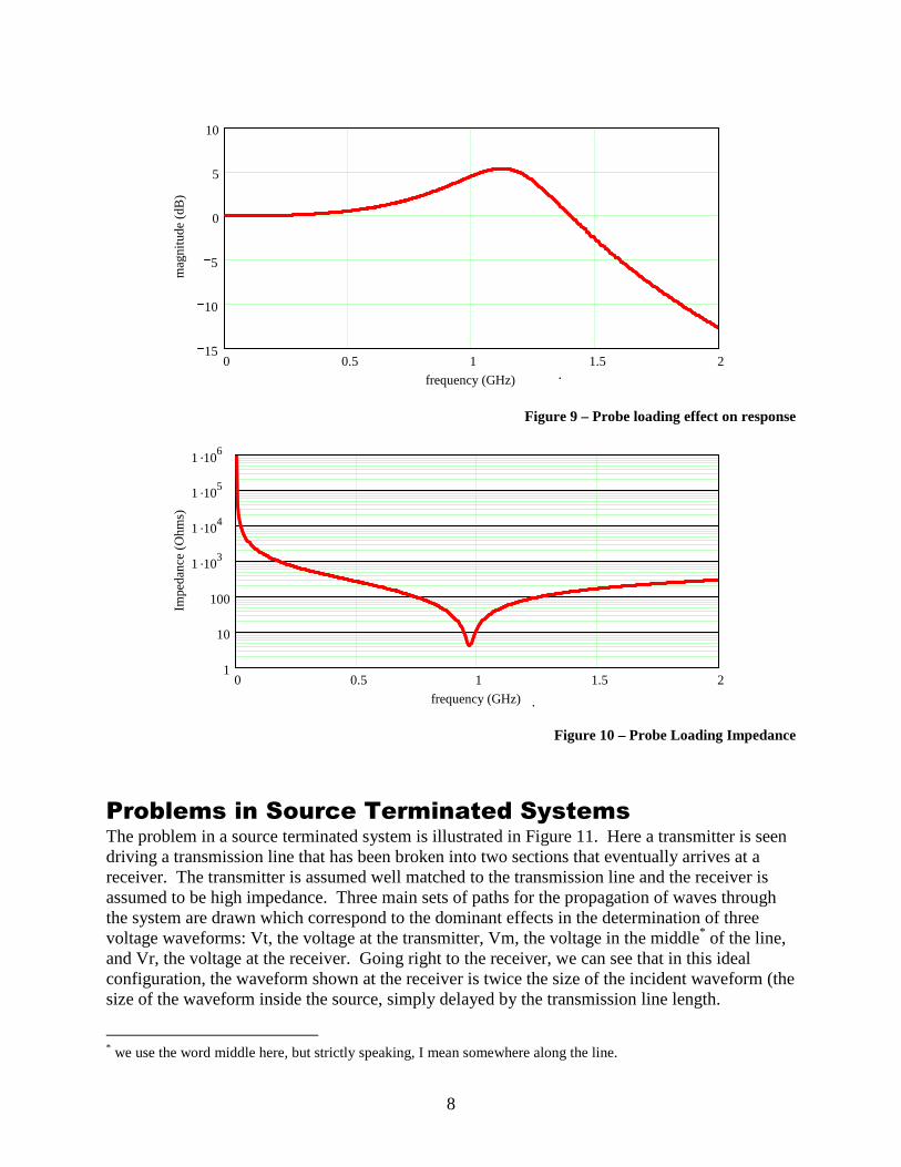
Probe Model When (or even before) results like those shown in Figure 7 are obtained, one should always look carefully at the effects of the probe. For this particular measurement, a 1.5 GHz probe was utilized that has a loading model as shown in Figure 8. We assumed 25 nH/in. for the wires used to connect the probe tips to the exposed circuit vias.
Figure 8 – Probe Loading Model
This model leads to a probe loading effect as shown in Figure 10, and a loading effect on the magnitude response Considering the fact that the clock signal is at 214 MHz clock, the third harmonic appears at 642 MHz and should be acquired with no problem. If the fifth harmonic is required, then it sits at the main resonance of the probe loading, but examining Figure 7 the non-monotonicity problem is clearly a third harmonic effect. The conclusion, therefore, from looking at the probe model and the probe loading effect is that while there are effects worth accounting for, the probe is not the source of the non-monotonicity found.
8
τ
0 0.5 1 1.5 215
10
5
0
5
10
frequency (GHz)
mag
nitu
de (
dB)
.
Figure 9 – Probe loading effect on response
0 0.5 1 1.5 21
10
100
1 .103
1 .104
1 .105
1 .106
frequency (GHz)
Impe
danc
e (O
hms)
.
Figure 10 – Probe Loading Impedance
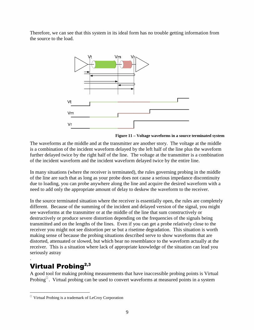
Problems in Source Terminated Systems The problem in a source terminated system is illustrated in Figure 11. Here a transmitter is seen driving a transmission line that has been broken into two sections that eventually arrives at a receiver. The transmitter is assumed well matched to the transmission line and the receiver is assumed to be high impedance. Three main sets of paths for the propagation of waves through the system are drawn which correspond to the dominant effects in the determination of three voltage waveforms: Vt, the voltage at the transmitter, Vm, the voltage in the middle* of the line, and Vr, the voltage at the receiver. Going right to the receiver, we can see that in this ideal configuration, the waveform shown at the receiver is twice the size of the incident waveform (the size of the waveform inside the source, simply delayed by the transmission line length.
* we use the word middle here, but strictly speaking, I mean somewhere along the line.
9
Therefore, we can see that this system in its ideal form has no trouble getting information from the source to the load.
Figure 11 – Voltage waveforms in a source terminated system
The waveforms at the middle and at the transmitter are another story. The voltage at the middle is a combination of the incident waveform delayed by the left half of the line plus the waveform further delayed twice by the right half of the line. The voltage at the transmitter is a combination of the incident waveform and the incident waveform delayed twice by the entire line. In many situations (where the receiver is terminated), the rules governing probing in the middle of the line are such that as long as your probe does not cause a serious impedance discontinuity due to loading, you can probe anywhere along the line and acquire the desired waveform with a need to add only the appropriate amount of delay to deskew the waveform to the receiver. In the source terminated situation where the receiver is essentially open, the rules are completely different. Because of the summing of the incident and delayed version of the signal, you might see waveforms at the transmitter or at the middle of the line that sum constructively or destructively or produce severe distortion depending on the frequencies of the signals being transmitted and on the lengths of the lines. Even if you can get a probe relatively close to the receiver you might not see distortion per se but a risetime degradation. This situation is worth making sense of because the probing situations described serve to show waveforms that are distorted, attenuated or slowed, but which bear no resemblance to the waveform actually at the receiver. This is a situation where lack of appropriate knowledge of the situation can lead you seriously astray .
Virtual Probing2,3 A good tool for making probing measurements that have inaccessible probing points is Virtual Probing. Virtual probing can be used to convert waveforms at measured points in a system
Virtual Probing is a trademark of LeCroy Corporation
10
(measurement nodes) to waveforms present at other points in a system under the same or different measurement conditions (output nodes). It can be used provided:
1. The characteristics of the circuit or circuits are known. 2. The sources of all waveforms that enter the circuit are known (i.e. all sources have been
identified). 3. The system can be assumed linear. 4. There is frequency content in the waveform at the measurement nodes at frequencies
which contain useful information in the waveforms at the output nodes. Item 4 simply means that if no signal content at a particular frequency gets to the probing point, no amount of processing can produce the waveform at a desired output point at that same frequency. We shall see later that in this application in particular, this can be a problem. The virtual probing configuration for this problem is shown schematically in Figure 12. Here we show two parallel circuit configurations. The bottom configuration is referred to as the measurement condition. It contains the probe model and a measurement node. It is assumed that during the use of virtual probing, the waveform at the measurement node will be provided to the oscilloscope. The top configuration is referred to as the output condition. It is the circuit configuration under which the output signals are desired. There are several output nodes in this circuit. All of these output nodes are produced based on the measured waveform at the measurement node VP. These are:
1. VT – The voltage waveform at the transmitter with no probe connected. 2. VM – The voltage waveform at the probing point with no probe connected. 3. VR – The voltage waveform at the receiver with no probe connected. 4. VTP – The voltage waveform at the transmitter with the probe connected. 5. VPR – The voltage waveform at the receiver with the probe connected.
Here, the desire is to see VR, but it is useful to see the other waveforms to see the effects of probing on the system.

11
Figure 12 – Virtual probing configuration
In Figure 12, many of the elements are listed as ideal elements or as lumped elements, as in the probe loading model. Other more important elements of the system are listed as s-parameter files. Usually, the method of obtaining the circuit characteristics is to obtain measurements of the sections making up the circuit model. As all of the characteristics stated here are specified as s-parameters, one should obtain these measurements using a vector network analyzer (VNA) or through the use of time-domain reflectometry (TDR). Unfortunately in this particular case measurements like this were unavailable and were instead generated through simulations. In our first attempt at using virtual probing, models of the transmission line sections associated with the line to the left and to the right of the probing point were used in a netlist as shown in Figure 13 and the component was used in the processing web as shown in Figure 14.
Figure 13 – Virtual probing net-list
In this configuration, we were unable to obtain proper measurements of the waveforms at the receiver and we spent quite a bit of time trying to straighten things out. What we needed was a
12
better understanding of the situation and a better method for validating the models that we were using in the first place. In the end, we were able to obtain good measurements. It is the process of using simulation, the virtual probing technique and understanding of the theory simultaneously in this particular situation that we the authors would like to highlight in this paper. This method is described in the next section.
Figure 14 – Virtual probing configuration in processing web
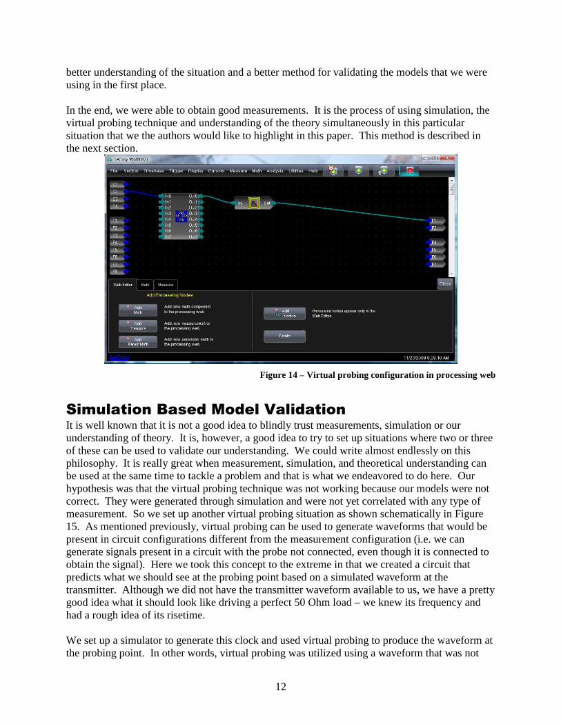
Simulation Based Model Validation It is well known that it is not a good idea to blindly trust measurements, simulation or our understanding of theory. It is, however, a good idea to try to set up situations where two or three of these can be used to validate our understanding. We could write almost endlessly on this philosophy. It is really great when measurement, simulation, and theoretical understanding can be used at the same time to tackle a problem and that is what we endeavored to do here. Our hypothesis was that the virtual probing technique was not working because our models were not correct. They were generated through simulation and were not yet correlated with any type of measurement. So we set up another virtual probing situation as shown schematically in Figure 15. As mentioned previously, virtual probing can be used to generate waveforms that would be present in circuit configurations different from the measurement configuration (i.e. we can generate signals present in a circuit with the probe not connected, even though it is connected to obtain the signal). Here we took this concept to the extreme in that we created a circuit that predicts what we should see at the probing point based on a simulated waveform at the transmitter. Although we did not have the transmitter waveform available to us, we have a pretty good idea what it should look like driving a perfect 50 Ohm load – we knew its frequency and had a rough idea of its risetime. We set up a simulator to generate this clock and used virtual probing to produce the waveform at the probing point. In other words, virtual probing was utilized using a waveform that was not
13
measured, but instead simulated to produce what we should be measuring at the probing point. This is a completely reverse usage of what virtual probing was intended for, but it allows us to get an idea of what we should see at the probing point.
Figure 15 – Simulator based virtual probing schematic
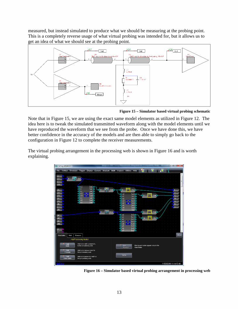
Note that in Figure 15, we are using the exact same model elements as utilized in Figure 12. The idea here is to tweak the simulated transmitted waveform along with the model elements until we have reproduced the waveform that we see from the probe. Once we have done this, we have better confidence in the accuracy of the models and are then able to simply go back to the configuration in Figure 12 to complete the receiver measurements. The virtual probing arrangement in the processing web is shown in Figure 16 and is worth explaining.
Figure 16 – Simulator based virtual probing arrangement in processing web

14
Figure 16 shows a feature of LeCroy oscilloscopes called the processing web4. The processing web is an environment for defining math processing and defines the particular processing used along with the waveform connections between processors. To the left of the web, all possible waveform and parameters are shown. To the right of the web, all possible outputs that have been configured as processing web outputs are shown. The area between is a playpen where users can drop down math processors and connect inputs and outputs together. We refer to the various math processors as simply processors. In Figure 16, a simulator component is shown connected to channel 2 and provides the math function F1. The simulator, in its final configuration is set to provide a 214.3 MHz clock with a risetime of 200 ps and is provided to the first virtual probe processor which is providing measurements based on the schematic in Figure 15. Therefore, its output is what should be seen at the probing point when the simulated transmitter is driven into the circuit in Figure 15 and provides math function F2. This waveform is passed on to a second virtual probe component which is the component that provides the desired waveform at the receiver as previously described as math function F3. F3 therefore is the waveform at the receiver provided a probed waveform in the middle of the line with that probed waveform generated based on a simulation of the transmitter. The memory trace M1 provides a stored waveform actually acquired by probing at the probing point in the actual circuit and is shown going through a deskew processor to align the time with the simulated version and is provided to math trace F4. It is supplied to a virtual probe component with the exact same configuration and netlist as the one above it – to provide the desired waveform at the receiver to math trace F5, except that this is the real waveform at the receiver due to the waveform that was truly probed at the probing point. What we found originally was not a surprise – that the simulated waveform at the probing point (F2) did not match the waveform actually acquired at the probing point (F4) because the models generated through spice simulation were not correct. It turned out that they did not properly account for an extra section of trace and bond-wire inside the memory package. When the models were adjusted to properly account for this, we were able to reproduce the probed waveform and simultaneously produce a virtual probing configuration that produced the desired waveform at the receiver – this again because we were using the exact same models in all virtual probing arrangements. The result of this exercise is shown in Figure 17.
15
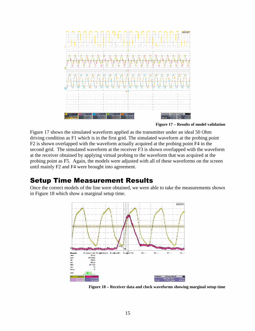
Figure 17 – Results of model validation
Figure 17 shows the simulated waveform applied as the transmitter under an ideal 50 Ohm driving condition as F1 which is in the first grid. The simulated waveform at the probing point F2 is shown overlapped with the waveform actually acquired at the probing point F4 in the second grid. The simulated waveform at the receiver F3 is shown overlapped with the waveform at the receiver obtained by applying virtual probing to the waveform that was acquired at the probing point as F5. Again, the models were adjusted with all of these waveforms on the screen until mainly F2 and F4 were brought into agreement.
Setup Time Measurement Results Once the correct models of the line were obtained, we were able to take the measurements shown in Figure 18 which show a marginal setup time.
Figure 18 – Receiver data and clock waveforms showing marginal setup time

16
The root cause of the problem was traced to a drive strength problem at the transmitter. The NPU did not have the expected output drive. The problem was rectified by programming the NPU to have a higher drive strength, resulting in the better result shown in Figure 19.
Figure 19 – Receiver data and clock waveforms showing resolved setup problem
Virtual Probing Theory To describe how virtual probing works for this application, we start with a description of the circuit with no probe attached as shown in Figure 20 which has a corresponding signal flow diagram shown in Figure 215.
Figure 20 – Circuit with no probe attached
bs
TL TR RT
t1
t2 m2
m1
r2
r1
Figure 21 – Signal flow diagram corresponding to Figure 20

17
To describe Figure 21, we define a system characteristic matrix:
Γ−−−−−
−−−−
Γ−
=
10000
1000
0100
0010
0001
00001
2221
1211
2221
1211
r
TRTR
TRTR
TLTL
TLTL
t
S
[ 1 ]
A node vector:
( )Trrmmtt 121212=N
[ 2 ]
And a stimulus vector:
( )Tbs 00000=M
[ 3 ]
Such that: MNS =⋅
[ 4 ]
Since M has only one nonzero element, we can write [ 4 ], solving for N as:
( ) bs⋅= −1*
1SN
[ 5 ]
Furthermore, define a voltage vector:
( )TVrVmVt=V
[ 6 ]
And a voltage extraction matrix:
0
110000
001100
000011
Z⋅
=VE
[ 7 ]
Such that: NVEV ⋅=
[ 8 ]
Substituting [ 5 ] for N in [ 8 ]: ( ) bs⋅⋅= −
1*1SVEV
[ 9 ]

18
[ 9 ] defines all of the voltages present in the system with respect to a single stimulus bs . If any voltage in the system is known (i.e. measured) and defined by its index i in V and it is desired to know (i.e. output) another voltage in the system similarly defined by its index o in V , then we can apply a transfer function to the measured voltage to generate the output voltage:
( )( ) 1,
1
1,1
,i
o
i
oio −
−
⋅⋅
==SVE
SVE
V
VH
[ 10 ]
Note that [ 10 ] is independent of stimuli. Therefore:
ioio ,HVV ⋅=
[ 11 ]
The process described up to this point is useful for producing voltages at various points in a circuit given a known voltage at a given point. But so far, we have not provided a method for actually obtaining a voltage measurement – this we accomplish by repeating the process with a probe connected as in Figure 22
Figure 22 – Circuit with probe attached
Figure 22 presents a slight problem with regard to the signal flow diagram. This is because a signal flow diagram cannot have multiple port connections – like the probe connection point. To resolve this, we use an artificial device that mimics the simultaneous connections of the probe point and the left and right transmission line sections:
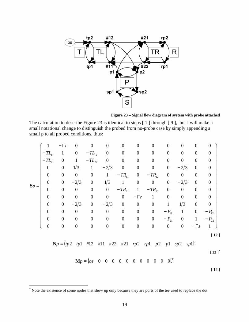
19
bs
TL TR RT
tp1
tp2 #21
#22
rp2
rp1
P
S
sp2sp1
#12
#11
p1 p2
Figure 23 – Signal flow diagram of system with probe attached
The calculation to describe Figure 23 is identical to steps [ 1 ] through [ 9 ], but I will make a small notational change to distinguish the probed from no-probe case by simply appending a small p to all probed conditions, thus:
Γ−−−−−
−−Γ−
−−−−
−−−−
−−−−
Γ−
=
10000000000
1000000000
0100000000
003110003203200
00001000000
0000100000
003200013103200
0000010000
003200003213100
0000000010
0000000001
00000000001
2221
1211
2221
1211
2221
1211
s
PP
PP
r
TRTR
TRTR
TLTL
TLTL
t
pS
[ 12 ]
( )Tspsppprprptptpp 12121221#22#11#12#12=N
[ 13 ]*
( )Tbsp 00000000000=M
[ 14 ]
* Note the existence of some nodes that show up only because they are ports of the tee used to replace the dot.

20
0
110000000000
001100000000
000011000000
000000000011
Zp ⋅
=VE
[ 15 ]*
( )TVspVpVrpVtpp =V
[ 16 ]
( ) bsppp ⋅⋅= −1*
1SVEV
[ 17 ]†
It is interesting and useful to note that while [ 17 ] defines voltages in the system with a probe present and [ 9 ] defines voltages in the system with no probe present, because bs is the same, both equations can be utilized in [ 10 ] and [ 11 ] to generate transfer functions. In other words, transfer functions can be generated by measuring signals in the probed circuit to produce signals that would be present in the same circuit were the probe not present.
Virtual Probing in a Source Terminated Line To understand the basic situation in a source terminated line, we return to the system characteristics matrix in [ 1 ] and consider only an unprobed circuit for the moment. Even a system as small as described by the characteristics of [ 1 ] lead to equations that don’t fit on a page. Therefore, to provide some insight and smaller equations, we make some simplifications:
1. The transmitter is an ideal 50 Ohm load. 2. The left and right transmission line components are ideal transmission lines with matched
impedance. 3. The receiver is an ideal open.
The system characteristics matrix therefore becomes:
−−
−−
−
=
110000
01000
01000
00010
00010
000001
DR
DR
DL
DL
S
[ 18 ]
* Note that the voltage extraction matrix has columns removed to remove the duplicate voltages appearing at the tee. † The selection of column 1 of 1−pS comes about only because the nonzero element of pM is the same as that in
M .

21
Where: fTljfTrj eDLeDR ππ 22 , −− ==
[ 19 ]
Representing a fixed delay through each element. When we use [ 18 ] and solve [ 9 ] we obtain definitions of the voltages in terms of these delays and the driven source:
( ) ( )( ) bsZDLDRDRDLDLDRVrVmVtTT ⋅⋅⋅⋅+⋅⋅+== 0211 222V
[ 20 ]
This makes sense since:
1. The voltage at the transmitter is the sum of the outgoing wave and the wave delayed twice by the length of the entire line.
2. The voltage in the middle of the line is the sum of the outgoing wave delayed by the left transmission line portion and the wave delayed by the same amount and additionally the round trip distance to the transmitter given by the right transmission line portion.
3. The voltage at the receiver is twice as big and is delayed by the length of the entire line. In retrospect, we did not need this type of math to see these facts as were expressed graphically in Figure 11. [ 20 ] implies some bad things, however, for the concept of virtual probing. This is because if one creates a transfer function that converts the voltage probed in the middle of the line to the voltage at the receiver, we obtain:
( ) ( )22 1
2
1
2
DR
DR
DRDL
DLDRH rm +
⋅=+⋅
⋅⋅=→
[ 21 ]
Which is incidentally independent of the length of the left-hand transmission line portion. The denominator of [ 21 ] goes to zero whenever 21 DR+ goes to zero, or when DR goes to j , and therefore, whenever:
Trf
⋅=
4
1
[ 22 ]
Therefore, we’d like for f
Tr⋅
<4
1. Said differently, we really want to probe as close to the
receiver as possible in this application, where degree of closeness, as usual, is determined by the frequencies of interest.

22
When You Just Can’t Probe Close Enough… [ 22 ] places an interesting bound on the recovery of the receiver waveform based on the electrical distance between the probing point and the receiver. In our case, we had about 650 ps between the receiver and the probing point, which leads to a value of f in [ 22 ] of about 385 MHz. But our first clock harmonic occurs at around 214 MHz and the third harmonic therefore appears at 642 MHz, so clearly we are violating this rule. The implications of [ 22 ] are that it is impossible to use the frequency specified, because the transfer function goes to infinity at this point. It may however be possible to still make valid measurements with this frequency excluded. In fact, it will be necessary to ensure that all frequencies that cause [ 21 ] to go to infinity are excluded. These turn out to be all odd multiples of the frequency in [ 22 ]. So, in our particular case, we need to exclude 385 MHz and 1.15 GHz. The latter frequency posed no problem since it was outside our bandwidth of interest. The first frequency posed no problem with our clock signal since it occurs right in between the harmonics present. It is important to note, however, that even if the signals are not present in the input signal, oscilloscopes will produce noise and other artifacts that might be present at these frequencies. In this particular case, we could still use the virtual probing technique as long as we supplied filters. Here we use a low-pass filter to exclude any noise above 1 GHz and a band-stop filter to notch out any frequency content around 385 MHz. This filtering is shown in Figure 16 as a filter component between the top two virtual probe components. The locations of all of these components can be seen in Figure 24.
Figure 24 – Filter Considerations
It is interesting to note that because the two harmonics of interest in the clock waveform straddle the 385 MHz frequency, the phase of the transfer function goes rapidly from 0 to -180 degrees at the 385 MHz frequency point. Therefore, the non-monotonic shape of the clock waveform can be explained ideally as harmonic distortion. The harmonic distortion in this case causes the third harmonic to add destructively. This distortion can be seen graphically in Figure 25.

23
0 2 4 6 8 10 12 142
1.5
1
0.5
0
0.5
1
1.5
2
FundamentalThird HarmonicProper Assembly of HarmonicsImproper Out-of-phase HarmonicsDistortion from Phase and Gain Harmonic Mismatch
Harmonic Distortion
time (ns)
am
plitu
de (
V)
norm
aliz
ed
.
Figure 25 – Graphical representation of harmonic distortion
Summary A problem was described in a memory system whereby it was desirable to make setup measurements at the receiver in order to determine the problem cause. Because the signals could not be probed at the ideal locations and because the system involved source termination with no receive side termination, the probed waveforms were distorted. Steps were provided that showed how the waveforms at the receiver could be recovered despite the non-ideal probing points. Various considerations were explained in how to deal with this type of situation.
References 1 http://www.qdrconsortium.org/presentation/QDR_Overview_Oct02.pdf 2 P. J. Pupalaikis, “Advanced Tools for High Speed Serial Data Measurements”, DesignCon 2007, Feb 2007 3 P. J. Pupalaikis et al., “Virtual Probing”, US Patent Application 11/888,547, Aug 2007 4 A. Cake et al., “User Defined Processing Function”, US Patent 6,952,655, Dec 2002 5 “S-Parameter Design,” Hewlett Packard Application Note 154, March, 1990, (5952-1087).


![Chapter 6enters a password [2][3], timing of memory accesses under artificially-induced thrashing conditions [4], timing of disk I/O response times[5], and measurement of timing skew](https://static.fdocuments.in/doc/165x107/5ff21fc9cf931529293048aa/chapter-6-enters-a-password-23-timing-of-memory-accesses-under-artificially-induced.jpg)