![UNOFFICIAL/UNAUTHENTICATED TRANSCRIPT 26 July 2019.]€¦ · UNOFFICIAL/UNAUTHENTICATED TRANSCRIPT UNOFFICIAL/UNAUTHENTICATED TRANSCRIPT 24485 [The R.M.C. 803 session was called to](https://static.fdocuments.in/doc/165x107/5f07260f7e708231d41b8c44/unofficialunauthenticated-transcript-26-july-2019-unofficialunauthenticated.jpg)
TIMING CONSIDERATIONS - The Unofficial CP/M … basic timing diagram for a read cycle is shown in...
57
Design and PCB Layout Considerations for Dynamic Memories interfaced to the Z80 CPU by Tim Olmstead 10-01-96 Interfacing dynamic memories to microprocessors can be a demanding process. Getting DRAMs to work in your prototype board can be even tougher. If you can afford to pay for a multi-layer PCB for your prototype you will probably not have many problems. This paper is not for you. This paper is for the rest of us. I will break down the subject of DRAM interfacing into two categories; timing considerations for design, and layout considerations. Since information without application is only half the battle, this information will then be applied to the Z80 microprocessor. TIMING CONSIDERATIONS In this day, given the availability of SIMM modules it would be tempting to concentrate only on these parts. But, to do so would bypass a large supply of surplus parts that might be very attractive to homebuilders. We will then examine several different types of DRAM chips. The main distinction between these parts is whether they have bi-directional I/O pins, or separate IN and OUT pins. Another distinction will affect refresh. Will the device support CAS-before-RAS refresh, or not? Let's begin at the beginning. Let's have a look at some basic DRAM timing, and how we might implement it. Figure 1. Basic DRAM read timing. 1 RAS* CAS* ROW ADDRESS COL ADDR DON'T CARE
Transcript of TIMING CONSIDERATIONS - The Unofficial CP/M … basic timing diagram for a read cycle is shown in...
Design and PCB Layout Considerations for Dynamic Memories
interfaced to the Z80 CPUby
Tim Olmstead10-01-96
Interfacing dynamic memories to microprocessors can be a demanding process. Getting DRAMsto work in your prototype board can be even tougher. If you can afford to pay for a multi-layerPCB for your prototype you will probably not have many problems. This paper is not for you.This paper is for the rest of us.
I will break down the subject of DRAM interfacing into two categories; timing considerationsfor design, and layout considerations. Since information without application is only half thebattle, this information will then be applied to the Z80 microprocessor.
TIMING CONSIDERATIONS
In this day, given the availability of SIMM modules it would be tempting to concentrate only onthese parts. But, to do so would bypass a large supply of surplus parts that might be veryattractive to homebuilders. We will then examine several different types of DRAM chips. Themain distinction between these parts is whether they have bi-directional I/O pins, or separate INand OUT pins. Another distinction will affect refresh. Will the device support CAS-before-RASrefresh, or not?
Let's begin at the beginning. Let's have a look at some basic DRAM timing, and how we mightimplement it.
Figure 1. Basic DRAM read timing.
1
RAS*
CAS*
ROW ADDRESS COL ADDR DON'T CARE
The basic timing diagram for a read cycle is shown in figure 1 above. Two control signals areused to sequence the address into the device; RAS, or Row Address Strobe, and CAS, orColumn Address Strobe.
The address is multiplexed into dynamic memories to conserve package pins. To access a 64KDRAM device, you would need sixteen address lines. Without multiplexing, this would requiresixteen pins on the package. That's a lot of pins. By today's standards, a 64K DRAM is verysmall. To support a modern 16MB part you would need 24 pins. This would lead to some verylarge device packages, and reduce the number of them that you could place on a single PCB.
Multiplexing the addresses saves package pins, and allows the device to fit into a much smallerpackage, at the expense of a more complex circuit required to operate the devices whencompared to static rams. We will discuss a variety of DRAM devices here, but, for now, let'sstay with our 64K DRAM. This will be the smallest (in capacity) device we will discuss. It isincluded here because they are plentiful, and VERY cheap, on the surplus market. This wouldmake them ideal for use in hobbyist projects.
Let us review the timing diagram in figure 1. On the top row of the diagram we see RAS*. Thisis our Row Address Strobe. Next we see CAS*, the Column Address Strobe. At the bottom wesee the address lines that connect to the DRAM chip itself. OK. What is this diagram trying toshow us? First we present the row address to the DRAM chip. Some time later, we take RAS*low, or active. We wait a little while, then switch the address presented to the chip. Now wepresent the column address. After we present the column address, we wait a little while, thentake CAS* active; low. Since this is a read cycle, some time after CAS* goes low, the memorywill supply output data. Simple huh? Righhhhht! Ok. So how do we do it? What do we need tocreate this kind of timing? The following illustration will give us some hints.
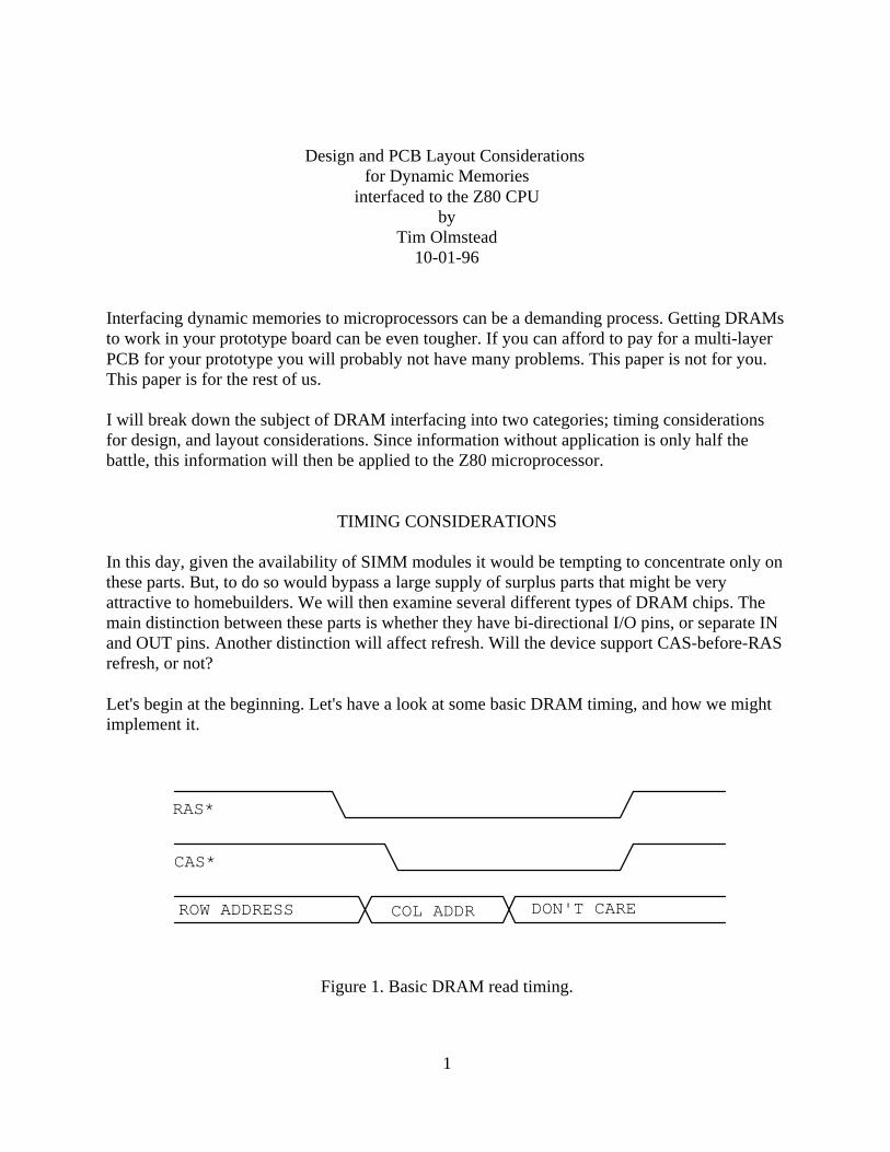
Figure 2. Basic DRAM Timing Generation
2
DELAY LINERAS* CAS*
MUX
A15
A0
74XX157(2 PCS)
4164
DYNAMIC
RAM
In figure 2 we see the basic dynamic memory controller circuit that has been in use since the late1970's. No, don't go out and grab your wire-wrap gun just yet. This circuit is not complete. Itdoes, however, illustrate the basic elements needed.
The key element in figure 2 is the delay line. This is a special part that will give precise delays.You feed a signal into the input, then take what you want at various "taps", or outputs. In thepast, delay lines were made from 7404 inverter packages. Sections were connected together toeliminate the inversion, and a coil inserted between sections to give the delay. The delay couldbe controlled by the number of turns of wire in the coils. Today, silicon delay lines are available.Dallas Semiconductor makes a line of silicon delay lines with very precise control of delays.They are pin compatible with the older mechanical ones, and cheaper too.
The first tap is used to generate a signal named MUX. This signal switches the 74xx157multiplexers to change from ROW address to COLUMN address. The second tap is then used togenerate CAS*. This circuit will provide the following timing.
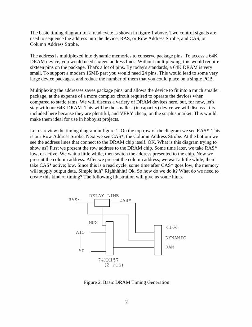
Figure 3. Timing for circuit in Fig 2.
As may be seen in Figure 3, our circuit generates the needed timing fairly well. The astute readerwill notice some overlap between CAS and RAS at the end of the cycle. This is not only O.K.,but some early DRAMs required it; notably, the 4116, 16k by 1.
Now let's examine a circuit to replace the delay line. If there is a high speed clock available inthe design, we can generate the timing with a shift register. This works best if the CPU clock isalso derived from this same source. Let's consider a 10 MHz Z80 design. We will use a 20 MHzoscillator module to derive timing from. The timing generation portion of the circuit in figure 2could look like this.
3
RAS*
CAS*
ROW ADDRESS COLUMN ADDRESS ROW ADDR
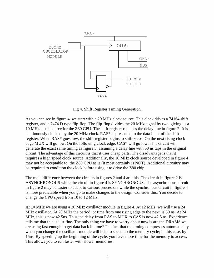
Fig 4. Shift Register Timing Generation.
As you can see in figure 4, we start with a 20 MHz clock source. This clock drives a 74164 shiftregister, and a 7474 D type flip-flop. The flip-flop divides the 20 MHz signal by two, giving us a10 MHz clock source for the Z80 CPU. The shift register replaces the delay line in figure 2. It iscontinuously clocked by the 20 MHz clock. RAS* is presented to the data input of the shiftregister. When RAS* goes low, the shift register begins to shift zeros. On the next rising clock edge MUX will go low. On the following clock edge, CAS* will go low. This circuit willgenerate the exact same timing as figure 3, assuming a delay line with 50 ns taps in the originalcircuit. The advantage of this circuit is that it uses cheap parts. The disadvantage is that itrequires a high speed clock source. Additionally, the 10 MHz clock source developed in figure 4may not be acceptable to the Z80 CPU as is (it most certainly is NOT). Additional circuitry maybe required to condition the clock before using it to drive the Z80 chip.
The main difference between the circuits in figures 2 and 4 are this. The circuit in figure 2 isASYNCHRONOUS while the circuit in figure 4 is SYNCHRONOUS. The asynchronous circuitin figure 2 may be easier to adapt to various processors while the synchronous circuit in figure 4is more predictable when you go to make changes to the design. Consider this. You decide tochange the CPU speed from 10 to 12 MHz.
At 10 MHz we are using a 20 MHz oscillator module in figure 4. At 12 MHz, we will use a 24MHz oscillator. At 20 MHz the period, or time from one rising edge to the next, is 50 ns. At 24MHz, this is now 42.5ns. Thus the delay from RAS to MUX to CAS is now 42.5 ns. Experiencetells me that this is just fine. The only thing we have to worry about now is are the DRAMS weare using fast enough to get data back in time? The fact that the timing compresses automaticallywhen you change the oscillator module will help to speed up the memory cycle; in this case, by15ns. By speeding up the beginning of the cycle, you have more time for the memory to access.This allows you to run faster with slower memories.
20MHZOSCILLATOR
MODULE
74164
7474
RAS*
CAS*
MUX
10 MHZTO CPU
4
With the circuit in figure 2 you can do the same thing, but you will need to replace the delay lineto get there. This could be a consideration when upgrading an existing design.
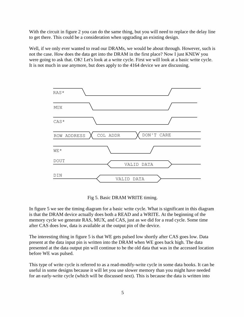
Well, if we only ever wanted to read our DRAMs, we would be about through. However, such isnot the case. How does the data get into the DRAM in the first place? Now I just KNEW youwere going to ask that. OK! Let's look at a write cycle. First we will look at a basic write cycle.It is not much in use anymore, but does apply to the 4164 device we are discussing.
Fig 5. Basic DRAM WRITE timing.
In figure 5 we see the timing diagram for a basic write cycle. What is significant in this diagramis that the DRAM device actually does both a READ and a WRITE. At the beginning of thememory cycle we generate RAS, MUX, and CAS, just as we did for a read cycle. Some timeafter CAS does low, data is available at the output pin of the device.
The interesting thing in figure 5 is that WE gets pulsed low shortly after CAS goes low. Datapresent at the data input pin is written into the DRAM when WE goes back high. The datapresented at the data output pin will continue to be the old data that was in the accessed locationbefore WE was pulsed.
This type of write cycle is referred to as a read-modify-write cycle in some data books. It can beuseful in some designs because it will let you use slower memory than you might have neededfor an early-write cycle (which will be discussed next). This is because the data is written into
RAS*
CAS*
ROW ADDRESS COL ADDR DON'T CARE
WE*
DOUT
DIN
VALID DATA
VALID DATA
MUX
5
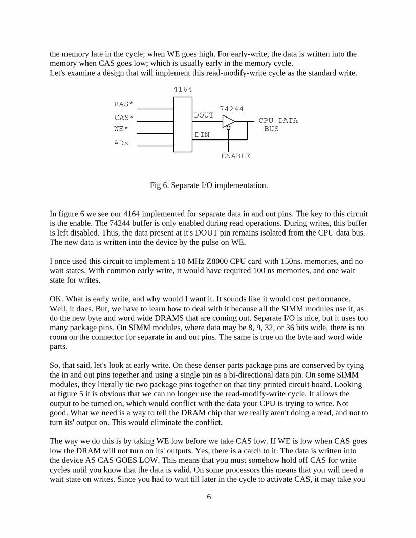
the memory late in the cycle; when WE goes high. For early-write, the data is written into thememory when CAS goes low; which is usually early in the memory cycle.Let's examine a design that will implement this read-modify-write cycle as the standard write.
Fig 6. Separate I/O implementation.
In figure 6 we see our 4164 implemented for separate data in and out pins. The key to this circuitis the enable. The 74244 buffer is only enabled during read operations. During writes, this bufferis left disabled. Thus, the data present at it's DOUT pin remains isolated from the CPU data bus.The new data is written into the device by the pulse on WE.
I once used this circuit to implement a 10 MHz Z8000 CPU card with 150ns. memories, and nowait states. With common early write, it would have required 100 ns memories, and one waitstate for writes.
OK. What is early write, and why would I want it. It sounds like it would cost performance.Well, it does. But, we have to learn how to deal with it because all the SIMM modules use it, asdo the new byte and word wide DRAMS that are coming out. Separate I/O is nice, but it uses toomany package pins. On SIMM modules, where data may be 8, 9, 32, or 36 bits wide, there is noroom on the connector for separate in and out pins. The same is true on the byte and word wideparts.
So, that said, let's look at early write. On these denser parts package pins are conserved by tyingthe in and out pins together and using a single pin as a bi-directional data pin. On some SIMMmodules, they literally tie two package pins together on that tiny printed circuit board. Lookingat figure 5 it is obvious that we can no longer use the read-modify-write cycle. It allows theoutput to be turned on, which would conflict with the data your CPU is trying to write. Notgood. What we need is a way to tell the DRAM chip that we really aren't doing a read, and not toturn its' output on. This would eliminate the conflict.
The way we do this is by taking WE low before we take CAS low. If WE is low when CAS goeslow the DRAM will not turn on its' outputs. Yes, there is a catch to it. The data is written intothe device AS CAS GOES LOW. This means that you must somehow hold off CAS for writecycles until you know that the data is valid. On some processors this means that you will need await state on writes. Since you had to wait till later in the cycle to activate CAS, it may take you
RAS*
CAS*
WE*
ADx
74244
4164
CPU DATABUS
ENABLE
DOUT
DIN
6
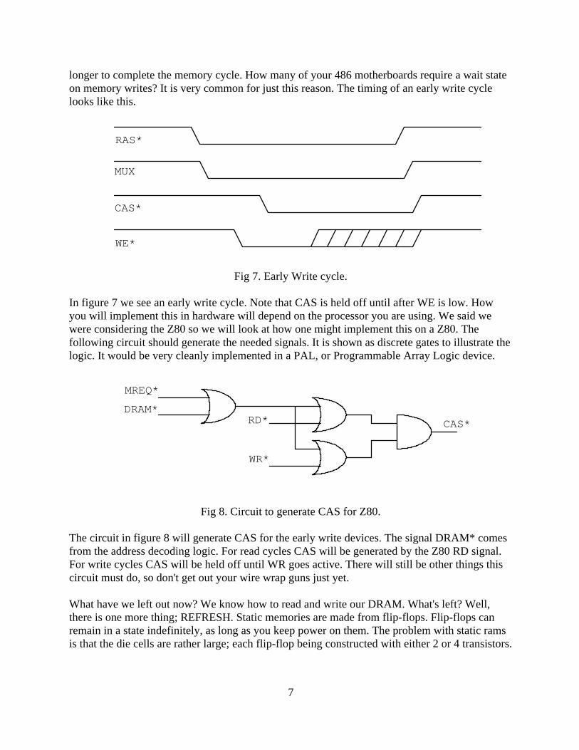
longer to complete the memory cycle. How many of your 486 motherboards require a wait stateon memory writes? It is very common for just this reason. The timing of an early write cyclelooks like this.
Fig 7. Early Write cycle.
In figure 7 we see an early write cycle. Note that CAS is held off until after WE is low. Howyou will implement this in hardware will depend on the processor you are using. We said wewere considering the Z80 so we will look at how one might implement this on a Z80. Thefollowing circuit should generate the needed signals. It is shown as discrete gates to illustrate thelogic. It would be very cleanly implemented in a PAL, or Programmable Array Logic device.
Fig 8. Circuit to generate CAS for Z80.
The circuit in figure 8 will generate CAS for the early write devices. The signal DRAM* comesfrom the address decoding logic. For read cycles CAS will be generated by the Z80 RD signal.For write cycles CAS will be held off until WR goes active. There will still be other things thiscircuit must do, so don't get out your wire wrap guns just yet.
What have we left out now? We know how to read and write our DRAM. What's left? Well,there is one more thing; REFRESH. Static memories are made from flip-flops. Flip-flops canremain in a state indefinitely, as long as you keep power on them. The problem with static ramsis that the die cells are rather large; each flip-flop being constructed with either 2 or 4 transistors.
RAS*
MUX
CAS*
WE*
MREQ*
DRAM*RD*
WR*
CAS*
7
In dynamic memories, the storage element is a capacitor. Just put a charge into the capacitor fora one, take it away for a zero. The problem with capacitors is that they won't hold their chargeforever. At least not without some help they won't. The reason capacitors won't hold their chargeis something called leakage. The charge is held on two plates, one with a positive charge, onewith a negative charge. The plates are held apart with some kind of insulator, or dielectric.Charge leaks between the plates through the dielectric. Now, wouldn't it be great if we put ourprogram in one of these capacitors, then came back a little later to run it, and it wasn't thereanymore? That is exactly what DRAMs would do without refresh.
Someone smarter than me decided that if you were to periodically go around to all of thecapacitors and freshen up the charge, that this just might work. Well, it does. To refresh aDRAM you must reference every row address in the device within a specified amount of time.
As DRAM devices get denser, that is bigger, they have more rows in them. The 4164 we've beentalking about has 256 rows; it uses 8 bits for the row address. A modern 4MB part has 2048rows, using 11 bits for the row address. This is eight times as many rows. If we had to refresh allrows in any device in the same amount of time, then with the 4MB part, we would need to runrefresh eight times as fast as for the 4164, just to get through in time.
Fortunately, this is not true. Over the years chip manufacturers have gotten the leakageperformance of each successive part a little better. Now we can basically refresh each part at thesame rate as the last one. This is good. If we had to keep refreshing faster and faster, we wouldsoon have no bandwidth left for the CPU to use the memory. We would be using all theavailable time to refresh it.
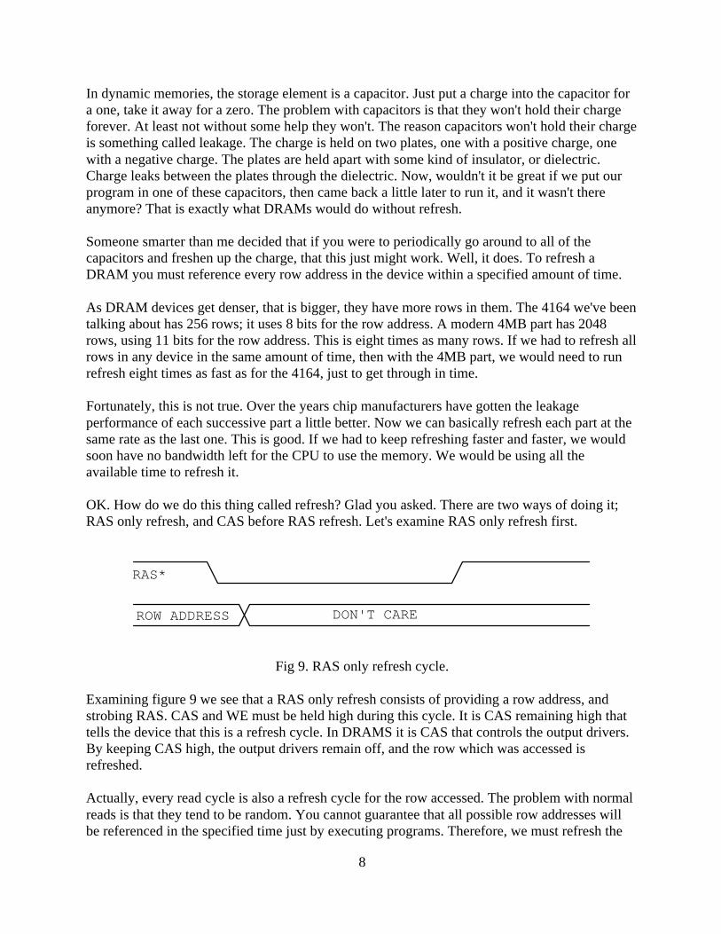
OK. How do we do this thing called refresh? Glad you asked. There are two ways of doing it;RAS only refresh, and CAS before RAS refresh. Let's examine RAS only refresh first.
Fig 9. RAS only refresh cycle.
Examining figure 9 we see that a RAS only refresh consists of providing a row address, andstrobing RAS. CAS and WE must be held high during this cycle. It is CAS remaining high thattells the device that this is a refresh cycle. In DRAMS it is CAS that controls the output drivers.By keeping CAS high, the output drivers remain off, and the row which was accessed isrefreshed.
Actually, every read cycle is also a refresh cycle for the row accessed. The problem with normalreads is that they tend to be random. You cannot guarantee that all possible row addresses willbe referenced in the specified time just by executing programs. Therefore, we must refresh the
RAS*
ROW ADDRESS DON'T CARE
8
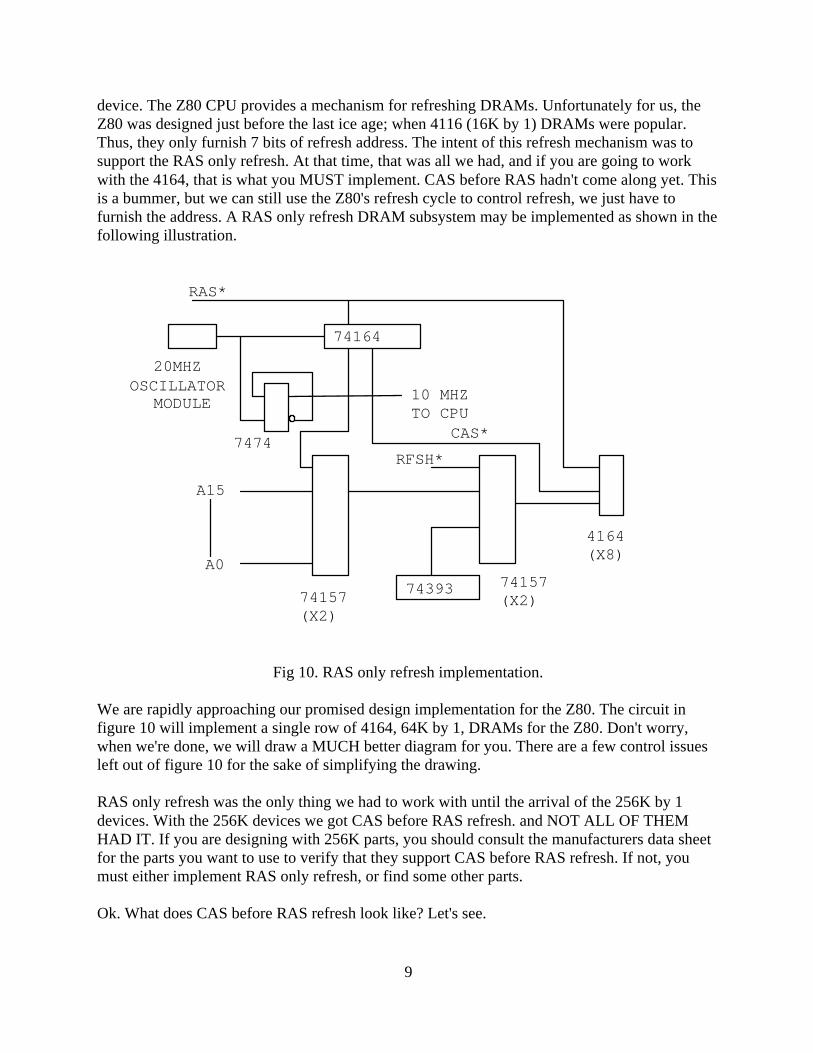
device. The Z80 CPU provides a mechanism for refreshing DRAMs. Unfortunately for us, theZ80 was designed just before the last ice age; when 4116 (16K by 1) DRAMs were popular.Thus, they only furnish 7 bits of refresh address. The intent of this refresh mechanism was tosupport the RAS only refresh. At that time, that was all we had, and if you are going to workwith the 4164, that is what you MUST implement. CAS before RAS hadn't come along yet. Thisis a bummer, but we can still use the Z80's refresh cycle to control refresh, we just have tofurnish the address. A RAS only refresh DRAM subsystem may be implemented as shown in thefollowing illustration.
RAS*
CAS*
74164
7474
74157(X2)
74393 74157(X2)
4164(X8)
A0
A15
20MHZOSCILLATOR
MODULE10 MHZTO CPU
RFSH*
Fig 10. RAS only refresh implementation.
We are rapidly approaching our promised design implementation for the Z80. The circuit infigure 10 will implement a single row of 4164, 64K by 1, DRAMs for the Z80. Don't worry,when we're done, we will draw a MUCH better diagram for you. There are a few control issuesleft out of figure 10 for the sake of simplifying the drawing.
RAS only refresh was the only thing we had to work with until the arrival of the 256K by 1devices. With the 256K devices we got CAS before RAS refresh. and NOT ALL OF THEMHAD IT. If you are designing with 256K parts, you should consult the manufacturers data sheetfor the parts you want to use to verify that they support CAS before RAS refresh. If not, youmust either implement RAS only refresh, or find some other parts.
Ok. What does CAS before RAS refresh look like? Let's see.
9
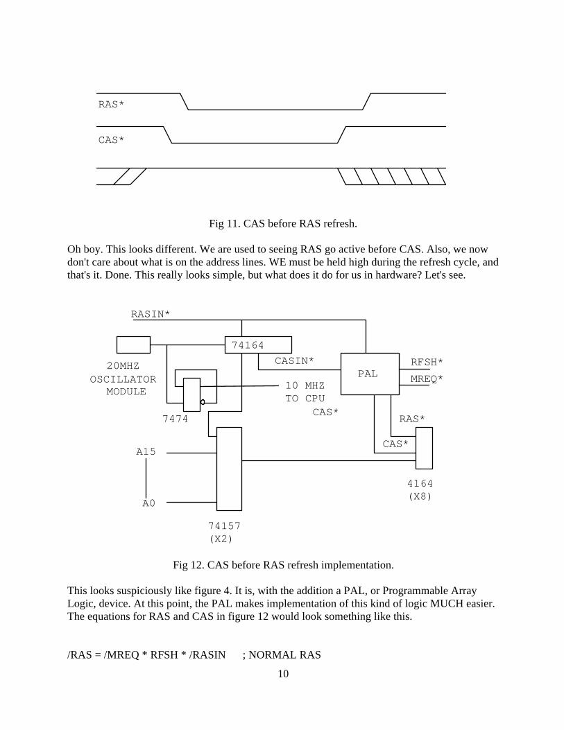
Fig 11. CAS before RAS refresh.
Oh boy. This looks different. We are used to seeing RAS go active before CAS. Also, we nowdon't care about what is on the address lines. WE must be held high during the refresh cycle, andthat's it. Done. This really looks simple, but what does it do for us in hardware? Let's see.
Fig 12. CAS before RAS refresh implementation.
This looks suspiciously like figure 4. It is, with the addition a PAL, or Programmable ArrayLogic, device. At this point, the PAL makes implementation of this kind of logic MUCH easier.The equations for RAS and CAS in figure 12 would look something like this.
/RAS = /MREQ * RFSH * /RASIN ; NORMAL RAS
RAS*
CAS*
RASIN*
CAS*
74164
7474
74157(X2)
4164(X8)
A0
A15
20MHZOSCILLATOR
MODULE10 MHZTO CPU
CASIN*
CAS*
RAS*
PALRFSH*
MREQ*
10
+ /MREQ * /RFSH * /CASIN ; REFSRESH
/CAS = /MREQ * RFSH * /CASIN ; NORMAL CAS+ /MREQ * /RFSH * /RASIN ; REFRESH
From the above equations it becomes quite clear how CAS before RAS refresh works. We stillhave our shift register generating the timing for us. For a normal memory cycle, we pass this onthrough. But, for a refresh cycle, we swap the outputs. The signal that is normally RAS goes toCAS, and the signal that is normally CAS goes to RAS. This implements the CAS before RASfunction very nicely. The processor will hold WR high during a refresh cycle, so there we are.The only thing left for us to do is to add in RD and WR. You did remember that we have to holdoff CAS for writes didn't you? Of course you did. The new equations would look like this.
/RAS = /MREQ * RFSH * /RASIN ; NORMAL RAS+ /MREQ * /RFSH * /CASIN ; REFSRESH
/CAS = /MREQ * RFSH * /CASIN * /RD ; NORMAL CAS FOR READ+ /MREQ * RFSH * /CASIN * /WR ; NORMAL CAS FOR WRITE+ /MREQ * /RFSH * /RASIN ; REFRESH
The memory subsystem shown in figure 12 may be implemented with any DRAM device thatsupports CAS before RAS refresh. With the equations above, you can also support early writeand use devices with a bi-directional data pin. Before we move on, let's examine some of thesedevices that might be of interest.
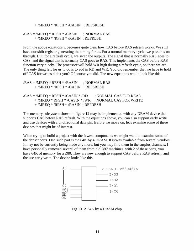
When trying to build a project with the fewest components we might want to examine some ofthe denser parts. One such part is the 64K by 4 DRAM. It is/was available from several vendors.It may not be currently being made any more, but you may find them in the surplus channels. Ihave personally removed several of them from old 286' machines. with 2 of these parts, youhave 64K of memory for a Z80. They are new enough to support CAS before RAS refresh, andthe use early write. The device looks like this.
Fig 13. A 64K by 4 DRAM chip.
A7
A 0R A SCASWEOE
I/O3
I/O2
I/O1
I/O0
VITELIC V53C464A
11
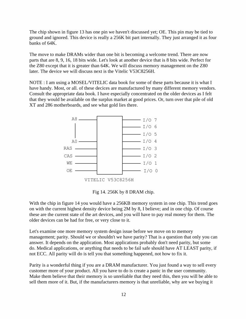
The chip shown in figure 13 has one pin we haven't discussed yet; OE. This pin may be tied toground and ignored. This device is really a 256K bit part internally. They just arranged it as fourbanks of 64K.
The move to make DRAMs wider than one bit is becoming a welcome trend. There are nowparts that are 8, 9, 16, 18 bits wide. Let's look at another device that is 8 bits wide. Perfect forthe Z80 except that it is greater than 64K. We will discuss memory management on the Z80later. The device we will discuss next is the Vitelic V53C8256H.
NOTE : I am using a MOSEL/VITELIC data book for some of these parts because it is what Ihave handy. Most, or all. of these decices are manufactured by many different memory vendors.Consult the appropriate data book. I have especially concentrated on the older devices as I feltthat they would be available on the surplus market at good prices. Or, turn over that pile of oldXT and 286 motherboards, and see what gold lies there.
Fig 14. 256K by 8 DRAM chip.
With the chip in figure 14 you would have a 256KB memory system in one chip. This trend goeson with the current highest density device being 2M by 8, I believe; and in one chip. Of coursethese are the current state of the art devices, and you will have to pay real money for them. Theolder devices can be had for free, or very close to it.
Let's examine one more memory system design issue before we move on to memorymanagement; parity. Should we or shouldn't we have parity? That is a question that only you cananswer. It depends on the application. Most applications probably don't need parity, but somedo. Medical applications, or anything that needs to be fail safe should have AT LEAST parity, ifnot ECC. All parity will do is tell you that something happened, not how to fix it.
Parity is a wonderful thing if you are a DRAM manufacturer. You just found a way to sell everycustomer more of your product. All you have to do is create a panic in the user community.Make them believe that their memory is so unreliable that they need this, then you will be able tosell them more of it. But, if the manufacturers memory is that unreliable, why are we buying it
A8
A0
RAS
CAS
WE
OE
I/O 7
I/O 6
I/O 5
I/O 4
I/O 3
I/O 2
I/O 1
I/O 0
VITELIC V53C8256H
12
in the first place? OK. I'll get down off my soapbox. If you think you really need parity, thenread on.
What is parity anyway. Well, put simply, it forces the number of bits set to a one across thestored word, including the parity bit, to be either even, or odd. For example, consider that thedata on the CPU's data bus is 00001111. To implement an even parity system, we would store azero in the parity bit. The byte we are generating parity for is already even since it has four bitsset to a one. By storing a zero in the parity bit, we still have an even number of bits set to a one.If we were implementing an odd parity system, we would store a one in the parity bit for thisexample. We would then have odd parity across all nine bits of the stored data.
I prefer to implement odd parity for DRAM systems. This ensures that there will be at least onebit in the group that is set to a one. Very often DRAM will come up with all zeroes in it afterpower up. If we implemented even parity we could read uninitialized memory, and not detect it.
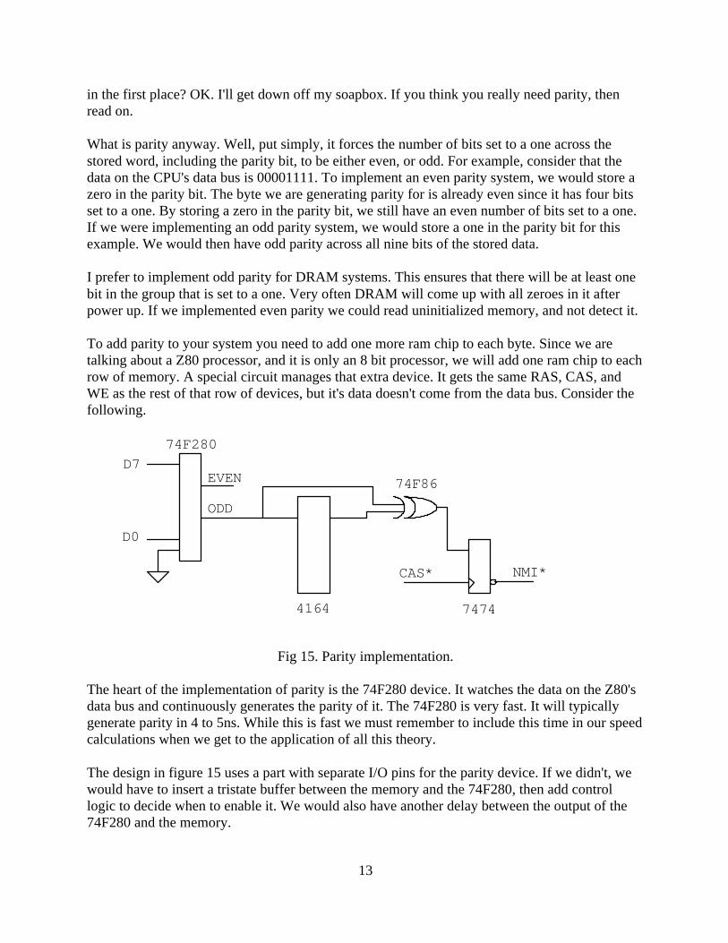
To add parity to your system you need to add one more ram chip to each byte. Since we aretalking about a Z80 processor, and it is only an 8 bit processor, we will add one ram chip to eachrow of memory. A special circuit manages that extra device. It gets the same RAS, CAS, andWE as the rest of that row of devices, but it's data doesn't come from the data bus. Consider thefollowing.
Fig 15. Parity implementation.
The heart of the implementation of parity is the 74F280 device. It watches the data on the Z80'sdata bus and continuously generates the parity of it. The 74F280 is very fast. It will typicallygenerate parity in 4 to 5ns. While this is fast we must remember to include this time in our speedcalculations when we get to the application of all this theory.
The design in figure 15 uses a part with separate I/O pins for the parity device. If we didn't, wewould have to insert a tristate buffer between the memory and the 74F280, then add controllogic to decide when to enable it. We would also have another delay between the output of the74F280 and the memory.
NMI*CAS*
D0
D7
74F280
4164 7474
74F86
ODD
EVEN
13
During a write cycle the parity is written into the parity ram. When the data is read back out ofmemory and placed on the CPUs data bus, the 74F280 generates the parity on the data just readback. The results are fed to the 74F86 XOR gate along with the value read back from the parityram. If they are both the same there will be a zero on the output of the XOR gate. This value issampled at the end of the memory cycle when CAS goes back high. If the generated parity doesnot agree with the parity stored in the extra ram an interrupt will be generated. System softwarewill then have to figure out what to do about it.
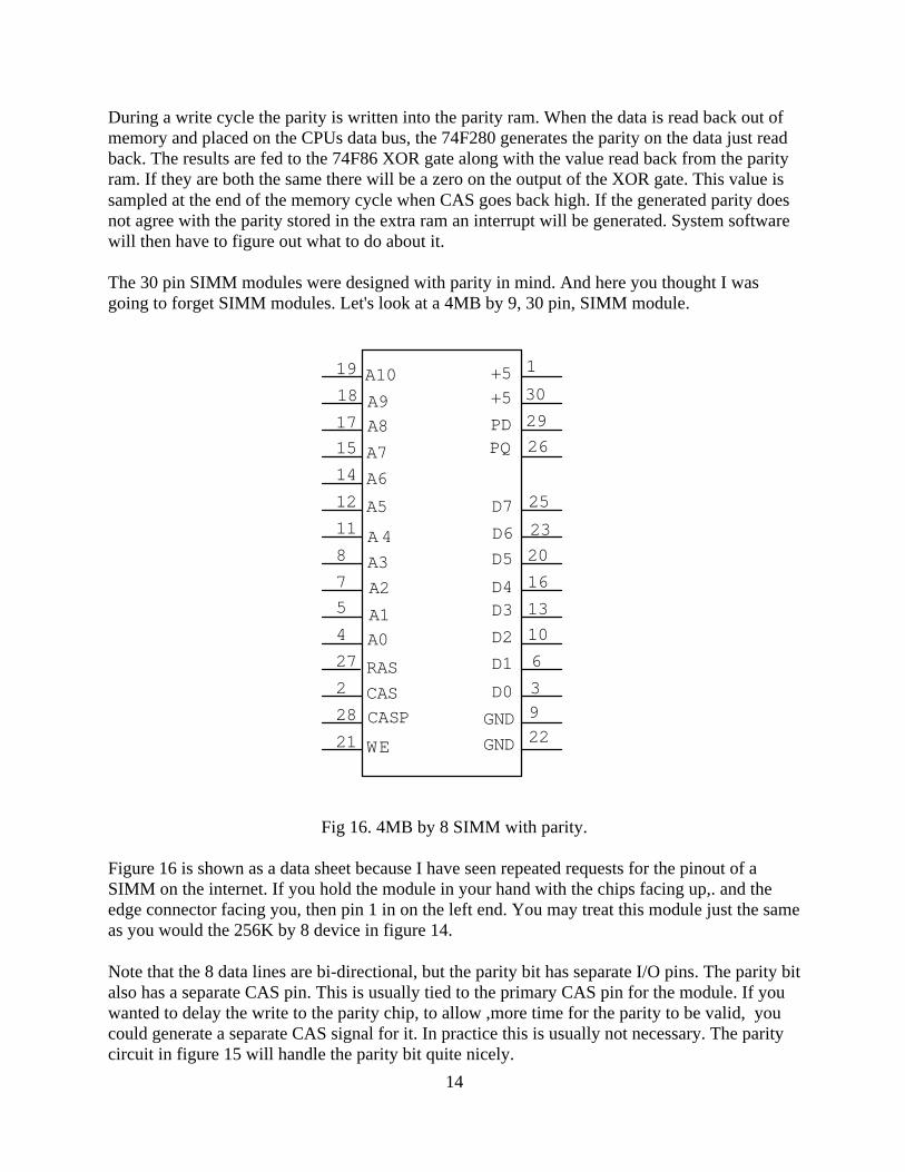
The 30 pin SIMM modules were designed with parity in mind. And here you thought I wasgoing to forget SIMM modules. Let's look at a 4MB by 9, 30 pin, SIMM module.
Fig 16. 4MB by 8 SIMM with parity.
Figure 16 is shown as a data sheet because I have seen repeated requests for the pinout of aSIMM on the internet. If you hold the module in your hand with the chips facing up,. and theedge connector facing you, then pin 1 in on the left end. You may treat this module just the sameas you would the 256K by 8 device in figure 14.
Note that the 8 data lines are bi-directional, but the parity bit has separate I/O pins. The parity bitalso has a separate CAS pin. This is usually tied to the primary CAS pin for the module. If youwanted to delay the write to the parity chip, to allow ,more time for the parity to be valid, youcould generate a separate CAS signal for it. In practice this is usually not necessary. The paritycircuit in figure 15 will handle the parity bit quite nicely.
A10
A9
A8
A7
A6
A5
A 4
A3
A2
A1
A0
RAS
CAS
CASP
WE
PDPQ
D7
D6
D5
D4D3
D2
D1
D0
+5
+5
GND
GND
9
22
1
30
29
26
25
23
20
16
13
10
6
3
21
28
2
27
4
5
7
8
11
12
14
15
17
18
19
14
For a number of reasons 30 pin SIMMs should be seriously considered for any home-brewproject. Using a SIMM module may spell the difference between success and not success foryour project; especially if it is hand wired. The SIMM module already has a PCB with theDRAMs mounted on it. It also has the correct bypass capacitors mounted under the DRAMchips. This gives you a step up on the most difficult part of implementing DRAMs in a prototypeenvironment; power distribution.
Another reason for considering using 30 pin SIMM modules is that the industry is moving on tothe 72 pin modules. it is now fairly easy to find 256K, 30 pin, SIMMs cheap. One surplus storenear me has them for $3.95 each. The 1MB and up parts are still in demand, and the price onthem is actually going up. Oh well. That's what supply and demand will do for you.
We will not discuss the 72 pin modules here. They are 32 bits wide. Our stated goal was tointerface memory to a Z80 which is 8 bits wide. While we could implement the module as fourbanks of 8 bit memory this is kind of esoteric and we won't do it. Should I get a flood ofrequests, we'll see.
APPLICATIONS
Oh boy. Now we get to the fun part. Here is where we try to make it work. We will considerseveral configurations of memory, but first it might be good to examine the environment wewish to implement in; the Z80 CPU.
The Z80 is an 8 bit microprocessor. It uses 16 bits for memory addressing giving it the ability toaddress 64K of memory. This is not much by today's standards. It is possible to make the Z80address more memory by adding external circuitry. With this circuitry it would be possible tomake the Z80 address as much memory as we want; say 4GB. A Z80 addressing 4GB ofmemory might not be quite practical. After all, what would it do with it? However, something alittle more down to earth might be useful; say 256K, or 1-4MB.
The first thing we must understand is this. No matter what external circuit we come up with, theZ80 will only address 64K at any given moment in time. What we need is a way to changewhere in the PHYSICAL address space the Z80 is working from moment to moment. Thisfunction is called memory management. The circuit that performs the memory management iscalled an MMU, or Memory Management Unit.
Today everyone is probably experienced with running 386MAX, QEMM, or HIMEM on theirPC's. This is the memory management software that runs the MMU in our 386/486/Pentiumprocessors. The PC uses memory management for a different function than what we might use itfor in the Z80, since the 386/486/Pentium processors are inherently capable of directlyaddressing a full 4GB of memory. With the Z80, we need an MMU just to even get at all of thememory we may have in the system.
The basic idea of how a memory manager works is this. There is a large PHYSICAL memoryspace defined by the amount of memory plugged into the system. If you plugged in 256K of
15
memory, then your physical address space is 256K, and so on. When a memory manager mapsmemory for the Z80 processor, the 64K address space of the Z80 becomes the LOGICALaddress space.
The logical address space is broken up, by the MMU, into small chunks. The next thing we mustdecide is how big the chunks are. They can be as small as we want, say 512 bytes. For our Z80's64K logical address space we would need 128 pages in our MMU to implement this.
If we are building a multitasking system some or most of these MMU pages may need to berewritten each time we have a task switch. This greatly increases system overhead. We want thetask switch to be accomplished as fast as possible. The code we execute during the task switchdoesn't contribute to the running of our application task. It is just overhead.
We would also need to design hardware that could provide that many pages in our MMU. Wecould certainly do this, but it would increase our chip count, and the MMU may not be fastenough for our needs.
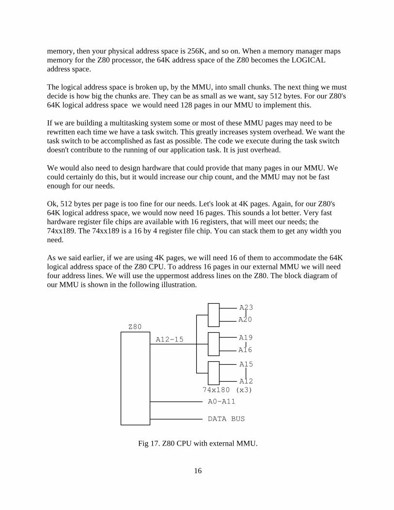
Ok, 512 bytes per page is too fine for our needs. Let's look at 4K pages. Again, for our Z80's64K logical address space, we would now need 16 pages. This sounds a lot better. Very fasthardware register file chips are available with 16 registers, that will meet our needs; the74xx189. The 74xx189 is a 16 by 4 register file chip. You can stack them to get any width youneed.
As we said earlier, if we are using 4K pages, we will need 16 of them to accommodate the 64Klogical address space of the Z80 CPU. To address 16 pages in our external MMU we will needfour address lines. We will use the uppermost address lines on the Z80. The block diagram ofour MMU is shown in the following illustration.
Fig 17. Z80 CPU with external MMU.
DATA BUS
A0-A11
A23
A20
A19
A16
A15
A12
Z80
A12-15
74x180 (x3)
16
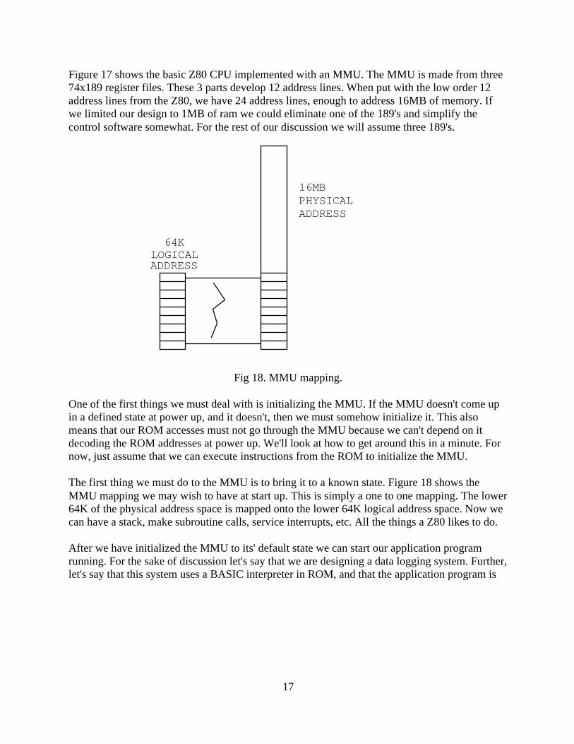
Figure 17 shows the basic Z80 CPU implemented with an MMU. The MMU is made from three74x189 register files. These 3 parts develop 12 address lines. When put with the low order 12address lines from the Z80, we have 24 address lines, enough to address 16MB of memory. Ifwe limited our design to 1MB of ram we could eliminate one of the 189's and simplify thecontrol software somewhat. For the rest of our discussion we will assume three 189's.
Fig 18. MMU mapping.
One of the first things we must deal with is initializing the MMU. If the MMU doesn't come upin a defined state at power up, and it doesn't, then we must somehow initialize it. This alsomeans that our ROM accesses must not go through the MMU because we can't depend on itdecoding the ROM addresses at power up. We'll look at how to get around this in a minute. Fornow, just assume that we can execute instructions from the ROM to initialize the MMU.
The first thing we must do to the MMU is to bring it to a known state. Figure 18 shows theMMU mapping we may wish to have at start up. This is simply a one to one mapping. The lower64K of the physical address space is mapped onto the lower 64K logical address space. Now wecan have a stack, make subroutine calls, service interrupts, etc. All the things a Z80 likes to do.
After we have initialized the MMU to its' default state we can start our application programrunning. For the sake of discussion let's say that we are designing a data logging system. Further,let's say that this system uses a BASIC interpreter in ROM, and that the application program is
64KLOGICALADDRESS
16MBPHYSICALADDRESS
17
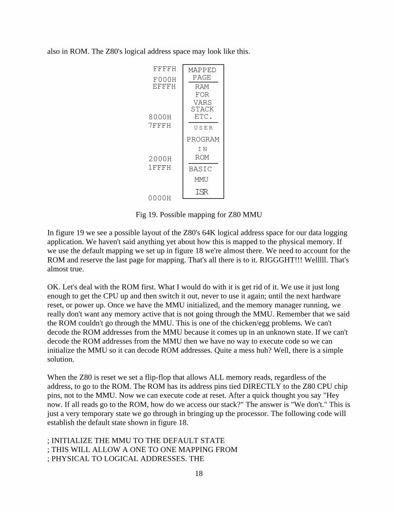
also in ROM. The Z80's logical address space may look like this.
Fig 19. Possible mapping for Z80 MMU
In figure 19 we see a possible layout of the Z80's 64K logical address space for our data loggingapplication. We haven't said anything yet about how this is mapped to the physical memory. Ifwe use the default mapping we set up in figure 18 we're almost there. We need to account for theROM and reserve the last page for mapping. That's all there is to it. RIGGGHT!!! Welllll. That'salmost true.
OK. Let's deal with the ROM first. What I would do with it is get rid of it. We use it just longenough to get the CPU up and then switch it out, never to use it again; until the next hardwarereset, or power up. Once we have the MMU initialized, and the memory manager running, wereally don't want any memory active that is not going through the MMU. Remember that we saidthe ROM couldn't go through the MMU. This is one of the chicken/egg problems. We can'tdecode the ROM addresses from the MMU because it comes up in an unknown state. If we can'tdecode the ROM addresses from the MMU then we have no way to execute code so we caninitialize the MMU so it can decode ROM addresses. Quite a mess huh? Well, there is a simplesolution.
When the Z80 is reset we set a flip-flop that allows ALL memory reads, regardless of theaddress, to go to the ROM. The ROM has its address pins tied DIRECTLY to the Z80 CPU chippins, not to the MMU. Now we can execute code at reset. After a quick thought you say "Heynow. If all reads go to the ROM, how do we access our stack?" The answer is "We don't." This isjust a very temporary state we go through in bringing up the processor. The following code willestablish the default state shown in figure 18.
; INITIALIZE THE MMU TO THE DEFAULT STATE; THIS WILL ALLOW A ONE TO ONE MAPPING FROM; PHYSICAL TO LOGICAL ADDRESSES. THE
0000H
1FFFH BASICMMU
ISR
7FFFH
2000H
U S E R
PROGRAMI N
ROM
8000H
EFFFHF000H
FFFFH
RAM
VARSSTACKETC.
FOR
MAPPEDPAGE
18
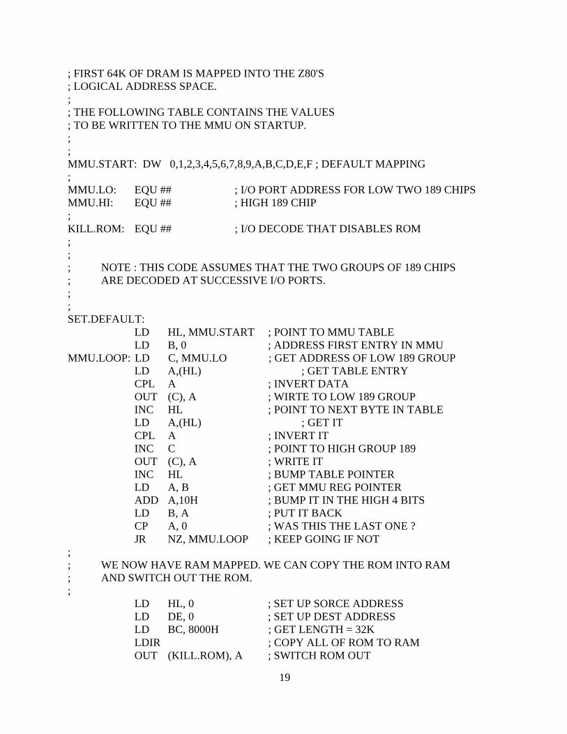
; FIRST 64K OF DRAM IS MAPPED INTO THE Z80'S ; LOGICAL ADDRESS SPACE.;; THE FOLLOWING TABLE CONTAINS THE VALUES; TO BE WRITTEN TO THE MMU ON STARTUP.;;MMU.START: DW 0,1,2,3,4,5,6,7,8,9,A,B,C,D,E,F ; DEFAULT MAPPING;MMU.LO: EQU ## ; I/O PORT ADDRESS FOR LOW TWO 189 CHIPSMMU.HI: EQU ## ; HIGH 189 CHIP;KILL.ROM: EQU ## ; I/O DECODE THAT DISABLES ROM;;; NOTE : THIS CODE ASSUMES THAT THE TWO GROUPS OF 189 CHIPS; ARE DECODED AT SUCCESSIVE I/O PORTS.;;SET.DEFAULT:
LD HL, MMU.START ; POINT TO MMU TABLELD B, 0 ; ADDRESS FIRST ENTRY IN MMU
MMU.LOOP: LD C, MMU.LO ; GET ADDRESS OF LOW 189 GROUPLD A,(HL) ; GET TABLE ENTRYCPL A ; INVERT DATAOUT (C), A ; WIRTE TO LOW 189 GROUPINC HL ; POINT TO NEXT BYTE IN TABLELD A,(HL) ; GET ITCPL A ; INVERT ITINC C ; POINT TO HIGH GROUP 189OUT (C), A ; WRITE ITINC HL ; BUMP TABLE POINTERLD A, B ; GET MMU REG POINTERADD A,10H ; BUMP IT IN THE HIGH 4 BITSLD B, A ; PUT IT BACKCP A, 0 ; WAS THIS THE LAST ONE ?JR NZ, MMU.LOOP ; KEEP GOING IF NOT
;; WE NOW HAVE RAM MAPPED. WE CAN COPY THE ROM INTO RAM; AND SWITCH OUT THE ROM.;
LD HL, 0 ; SET UP SORCE ADDRESSLD DE, 0 ; SET UP DEST ADDRESSLD BC, 8000H ; GET LENGTH = 32KLDIR ; COPY ALL OF ROM TO RAMOUT (KILL.ROM), A ; SWITCH ROM OUT
19
;; FROM HERE ON, WE ARE RUNNING IN RAM.;
LD SP, 7FFFH ; SET STACK..
The above code segment will handle MMU initialization. It first sets up the default mapping ofone to one. The first 64K of the physical address space is mapped onto the Z80's logical addressspace. Then the contents of the ROM are copied into the DRAM. (I never said that writescouldn't go to the dram). The LDIR instruction very nicely copies the first 32K, which is all ofthe ROM, into the dram, at the same logical address. We couldn't have done this until the MMUwas initialized.
Now, if we just had a couple of variables we could write a routine that would step the page inthe last MMU slot. If this routine were called repeatedly it would result in "walking" a windowthrough the entire address space. The window will appear in the last 4K of the Z80's logicaladdress space, 0F000H to 0FFFFH.
; THIS ROUTINE WILL STEP THE LAST PAGE OF THE MMU. SINCE WE ; CAN'T READ THE MMU WITH AN I/O INSTRUCTION, WE MUST KEEP; AN IMAGE OF WHAT WE PUT IN IT. THIS ROUTINE WILL ALSO MAKE; IT CLEAR WHY WE COMPLIMENT THE DATA BEFORE WRITING IT TO THE ; 189'S. IT IS A LOT EASIER TO DO BINARY ARITHMETIC ON POSTIIVE; NUMBERS. SINCE THE 189'S INVERT THE OUTPUTS, WE INVERT, OR; COMPLIMENT, THE NUMBER WE PUT IN, SO WE WILL GET OUT WHAT; WE WANT.;; IF THE MMU WRAPS AROUND 16MB, THEN THIS ROUTINE WILL RETURN ; WITH "NZ", OR "Z" IF NO ERROR;LAST.PAGE: DW 0FH ; INITIAL SETTING FOR LAST PAGE IN MMU;INC.MMU: LD HL, (LAST.PAGE) ; GET LAST PAGE VALUE
INC HL ; BUMP ITBIT 4, H ; DID WE WRAP AROUND 16MB?JR NZ, MMU.ERR ; ERROR IF SOLD (LAST.PAGE), HL ; SAVE NEW MMU VALUELD B, 0F0H ; POINT TO LAST MMU PAGELD C, MMU.LO ; GET POINTER TO WRITE TO MMULD A, L ; GET LSB BYTE OF NEW MMU ENTRYCPL A ; INVERT DATAOUT (C), A ; WIRTE TO LOW 189 GROUPLD A, H ; GET LSB BYTE OF NEW MMU ENTRYCPL A ; INVERT ITINC C ; POINT TO HIGH GROUP 189
20
OUT (C), A ; WRITE ITXOR A, A ; CLEAR Z FLAGRET ; SEND BACK GOOD COMPLETION
;MMU.ERR: LD A,0FFH ; SEND BACK ERROR
AND A, A ; TO CALLER BY SETTINGRET ; NZ
If we want to bump the MMU page the above code will do the job for us. When we overflow the16MB barrier we will get back an NZ status, and no change will be made in the MMU. I willleave it as an exercise for the student to figure out what would happen to the system if this testwere not included. What would happen? Oh heck, I can't keep a secret. It would start writingover memory at physical location 00000H. Since we put our BASIC interpreter, and interruptvectors there, the system would crash. All you would see of it is a little mushroom cloud overthe CPU chip.
When setting up the system memory map we must be sure of a couple of things. Certain thingsmust always be available. Some of these things are : Interrupt Service Routines, or ISRs,Interrupt/trap vector tables, and the MMU management code itself. For example, the routineshown above would need to be in common memory. At the least, it would not be good to loadthis routine anywhere in the range of 0F000H to 0FFFFH. If you did, the results would be asystem crash very alike to the one in the previous paragraph. The Z80 would be execution alonguntil it hit the first I/O instruction which changed the MMU page. After the write the MMUwould be pointing to a different place in memory and the next instruction fetched would not belikely to be what we want.
There is a way to make this work; you must make sure that the memory page you are switchingto also has a copy of the same routine, in the same place in memory. Then it would work. Whywould I ever want to do this? Well, let's consider another example application for our MMUcircuit; multi-tasking. Let's say that we want to set up a system to watch four serial lines. Whendata is presented from the SIO, we will store it in memory. To make it easy we would like towrite only one copy of the program, and let it multi-task to manage the four serial lines.
We will need to write a small multi-tasking kernel. It will handle setting up the four tasks, andany task switching we may need. We will assume a timer interrupt driven preemptivemulti-tasking environment. Since the serial lines are using interrupts we must have the ISRs incommon memory, or at least duplicated once per task.
21
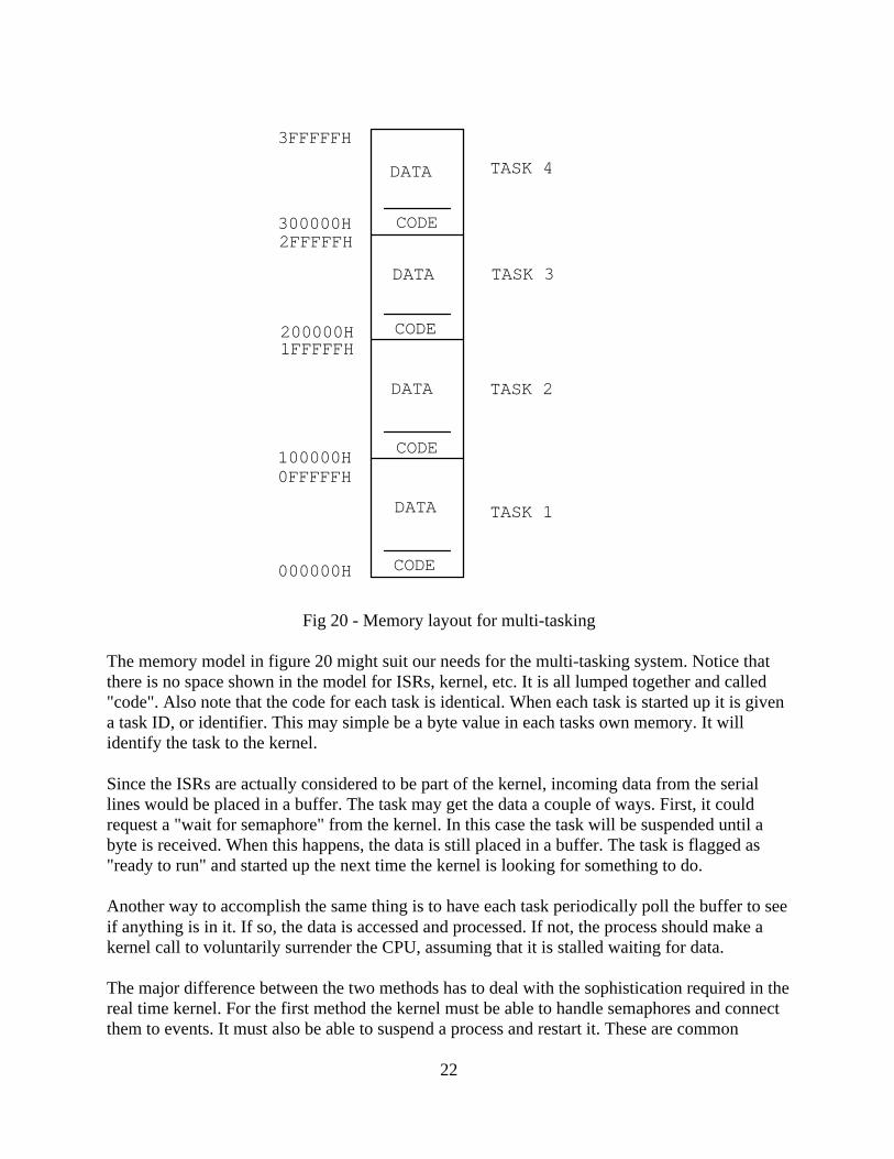
Fig 20 - Memory layout for multi-tasking
The memory model in figure 20 might suit our needs for the multi-tasking system. Notice thatthere is no space shown in the model for ISRs, kernel, etc. It is all lumped together and called"code". Also note that the code for each task is identical. When each task is started up it is givena task ID, or identifier. This may simple be a byte value in each tasks own memory. It willidentify the task to the kernel.
Since the ISRs are actually considered to be part of the kernel, incoming data from the seriallines would be placed in a buffer. The task may get the data a couple of ways. First, it couldrequest a "wait for semaphore" from the kernel. In this case the task will be suspended until abyte is received. When this happens, the data is still placed in a buffer. The task is flagged as"ready to run" and started up the next time the kernel is looking for something to do.
Another way to accomplish the same thing is to have each task periodically poll the buffer to seeif anything is in it. If so, the data is accessed and processed. If not, the process should make akernel call to voluntarily surrender the CPU, assuming that it is stalled waiting for data.
The major difference between the two methods has to deal with the sophistication required in thereal time kernel. For the first method the kernel must be able to handle semaphores and connectthem to events. It must also be able to suspend a process and restart it. These are common
000000H
100000H0FFFFFH
CODE
CODE
CODE
CODE
DATA
DATA
DATA
DATA
1FFFFFH200000H
2FFFFFH300000H
3FFFFFH
TASK 1
TASK 2
TASK 3
TASK 4
22
features of commercial real time kernels. Once such kernel I have worked with is the USX80kernel. It runs on a Z80 and provides all the features listed, and more.
In the second method, most of the "smarts" is moved to the application. A mechanism is requiredto switch tasks. This may be as simple as saving the machine state. I.E. : CPU registers andflags, to suspend a process. To restart the next process the kernel uses the task number to indexinto a table of MMU values and reprograms the MMU. If any MMU pages are allowed to bechanged, then they will need to be restored from variables stored in each tasks memory, after thelow MMU registers have been switched to point to the code space for the task. The tasks CPUregisters are then loaded back into the CPU, and the process restarted. This is fairly simple code.
The call made by the process to give up the CPU only forced a task switch. When a task lossesthe CPU because of a timer interrupt it is called preemptive multi-tasking. When a taskvoluntarily gives up the CPU it is called voluntary multi-tasking.
Both techniques may be combined in a system, and that is very appropriate for a Z80. In datalogging applications it is not hard to overrun the CPU if the data comes in too fast. If you haveone very high speed data channel, and the rest are of moderate data rate, the inclusion of thevoluntary task switch call may speed the system up considerably. The timer based task switchwill guarantee that no task can hog the CPU, but it does not allow you to recover idle time fromeach task by itself. You need both methods together to do that.
If implementing the simpler task switching system, my personal favorite, it would be a good ideato reinitialize the timer chip (within the kernel) when you execute the voluntary task switch. Thetimer interrupt will be asynchronous with respect to the task switch call so you don't know howmuch time remains before the timer will generate an interrupt. When you start the next task youwould like it to have a full time slice to run before it is interrupted.
Ok, so how do we initialize the memory model in figure 20? I'll bet you thought I'd forgottenthat, didn't you? We map the code space for each task into the upper 32K of the Z80's logicaladdress space, then block copy the code into it. The following code will do the trick. Assumethat initially we established our default memory map from figure 18. Now we will remap theupper 32K to map in the code space for each task in turn, and copy the code into it. Note that wedon't need to map TASK 0 since it is already mapped in by default.;;;MMU.DEFAULT: DW 0,1,.2,3,4,5,6,7,8,9,A,B,C,D,E,F ; DEAFULT MAPTASK1: DW 10H, 11H, 12H, 13H, 14H, 15H, 16H, 17H ; MAP ONLY 32KTASK2: DW 20H, 21H, 22H, 23H, 24H, 25H, 26H, 27H ; MAP ONLY 32KTASK3: DW 30H, 31H, 32H, 33H, 34H, 35H, 36H, 37H ; MAP ONLY 32K;; COPY CODE TO ALL TASK CODE AREAS.;COPY.TASK: LD HL, TASK1 ; POINT TO TASK 1 MMU TABLE
23
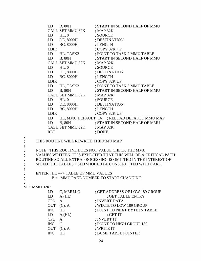
LD B, 80H ; START IN SECOND HALF OF MMUCALL SET.MMU.32K ; MAP 32KLD HL, 0 ; SOURCELD DE, 8000H ; DESTINATIONLD BC, 8000H ; LENGTHLDIR ; COPY 32K UPLD HL, TASK2 ; POINT TO TASK 2 MMU TABLELD B, 80H ; START IN SECOND HALF OF MMUCALL SET.MMU.32K ; MAP 32KLD HL, 0 ; SOURCELD DE, 8000H ; DESTINATIONLD BC, 8000H ; LENGTHLDIR ; COPY 32K UPLD HL, TASK3 ; POINT TO TASK 3 MMU TABLELD B, 80H ; START IN SECOND HALF OF MMUCALL SET.MMU.32K ; MAP 32KLD HL, 0 ; SOURCELD DE, 8000H ; DESTINATIONLD BC, 8000H ; LENGTHLDIR ; COPY 32K UPLD HL, MMU.DEFAULT+16 ; RELOAD DEFAULT MMU MAPLD B, 80H ; START IN SECOND HALF OF MMUCALL SET.MMU.32K ; MAP 32KRET ; DONE
;; THIS ROUTINE WILL REWRITE THE MMU MAP;; NOTE : THIS ROUTINE DOES NOT VALUE CHECK THE MMU ; VALUES WRITTEN. IT IS EXPECTED THAT THIS WILL BE A CRITICAL PATH; ROUTINE SO ALL EXTRA PROCESSING IS OMITTED IN THE INTEREST OF; SPEED. THE TABLES USED SHOULD BE CONSTRUCTED WITH CARE.;; ENTER : HL ==> TABLE OF MMU VALUES; B = MMU PAGE NUMBER TO START CHANGING;SET.MMU.32K:
LD C, MMU.LO ; GET ADDRESS OF LOW 189 GROUPLD A,(HL) ; GET TABLE ENTRYCPL A ; INVERT DATAOUT (C), A ; WIRTE TO LOW 189 GROUPINC HL ; POINT TO NEXT BYTE IN TABLELD A,(HL) ; GET ITCPL A ; INVERT ITINC C ; POINT TO HIGH GROUP 189OUT (C), A ; WRITE ITINC HL ; BUMP TABLE POINTER
24
LD A, B ; GET MMU REG POINTERADD A,10H ; BUMP IT IN THE HIGH 4 BITSLD B, A ; PUT IT BACKCP A, 0 ; WAS THIS THE LAST ONE ?JR NZ, SETMMU.32K ; KEEP GOING IF NOTRET ; EXIT WHEN DONE
The above code will take care of initializing the four tasks code area. Remember that we saidthat each task would use the same code. We just map in the code space for each task and copythe code to it. Simple! Now, since each task has the same image of the low 32K of memory wecan switch all of the MMU pages when we do a task switch if we want to.
Developing a complete multitasking kernel here would be beyond the scope of this paper, whichis implementing DRAM on the Z80. The MMU is an integral part of the memory system so wemust know how it works in order to implement our memory system.
Next, lets' look at how the Z80 uses memory.
THE Z80 CPU : TIMING
In an ideal world The Z80 would present us with only one set of timing for memory.Unfortunately, the world is not ideal. The Z80 CPU uses memory for two types of operations;instruction fetches, and data store/retreival. The timing for these operations is not the same. Thefollowing drawing shows an instruction fetch, or M1, cycle.
25
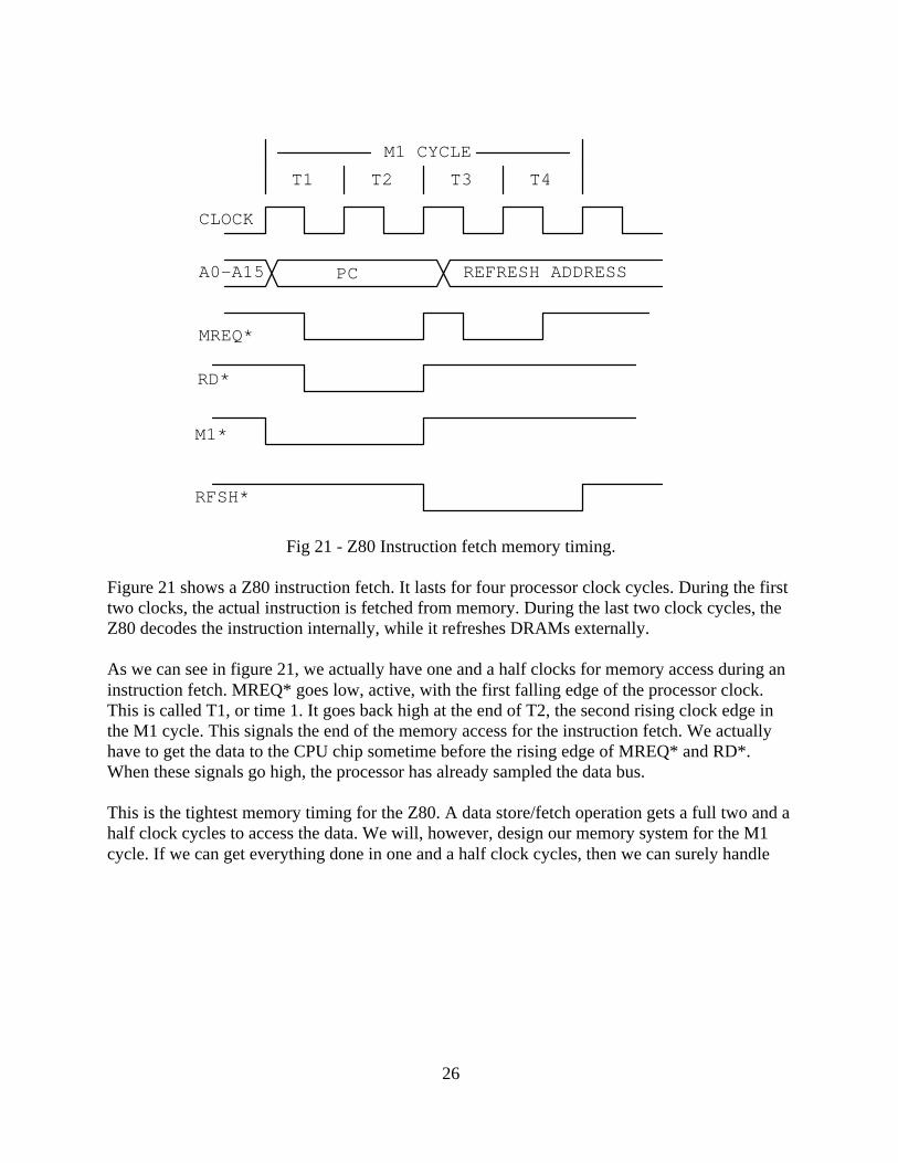
Fig 21 - Z80 Instruction fetch memory timing.
Figure 21 shows a Z80 instruction fetch. It lasts for four processor clock cycles. During the firsttwo clocks, the actual instruction is fetched from memory. During the last two clock cycles, theZ80 decodes the instruction internally, while it refreshes DRAMs externally.
As we can see in figure 21, we actually have one and a half clocks for memory access during aninstruction fetch. MREQ* goes low, active, with the first falling edge of the processor clock.This is called T1, or time 1. It goes back high at the end of T2, the second rising clock edge inthe M1 cycle. This signals the end of the memory access for the instruction fetch. We actuallyhave to get the data to the CPU chip sometime before the rising edge of MREQ* and RD*.When these signals go high, the processor has already sampled the data bus.
This is the tightest memory timing for the Z80. A data store/fetch operation gets a full two and ahalf clock cycles to access the data. We will, however, design our memory system for the M1cycle. If we can get everything done in one and a half clock cycles, then we can surely handle
CLOCK
PC REFRESH ADDRESSA0-A15
MREQ*
RFSH*
M1*
RD*
T1 T2 T3 T4
M1 CYCLE
26
the slower cycle.
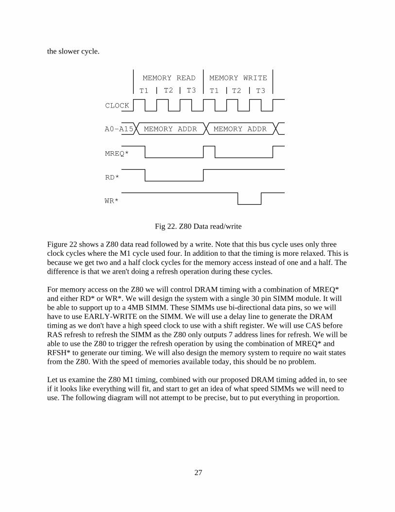
Fig 22. Z80 Data read/write
Figure 22 shows a Z80 data read followed by a write. Note that this bus cycle uses only threeclock cycles where the M1 cycle used four. In addition to that the timing is more relaxed. This isbecause we get two and a half clock cycles for the memory access instead of one and a half. Thedifference is that we aren't doing a refresh operation during these cycles.
For memory access on the Z80 we will control DRAM timing with a combination of MREQ*and either RD* or WR*. We will design the system with a single 30 pin SIMM module. It willbe able to support up to a 4MB SIMM. These SIMMs use bi-directional data pins, so we willhave to use EARLY-WRITE on the SIMM. We will use a delay line to generate the DRAMtiming as we don't have a high speed clock to use with a shift register. We will use CAS beforeRAS refresh to refresh the SIMM as the Z80 only outputs 7 address lines for refresh. We will beable to use the Z80 to trigger the refresh operation by using the combination of MREQ* andRFSH* to generate our timing. We will also design the memory system to require no wait statesfrom the Z80. With the speed of memories available today, this should be no problem.
Let us examine the Z80 M1 timing, combined with our proposed DRAM timing added in, to seeif it looks like everything will fit, and start to get an idea of what speed SIMMs we will need touse. The following diagram will not attempt to be precise, but to put everything in proportion.
CLOCK
A0-A15
MREQ*
RD*
WR*
MEMORY ADDR MEMORY ADDR
MEMORY READ MEMORY WRITE
T1 T2 T3 T1 T2 T3
27
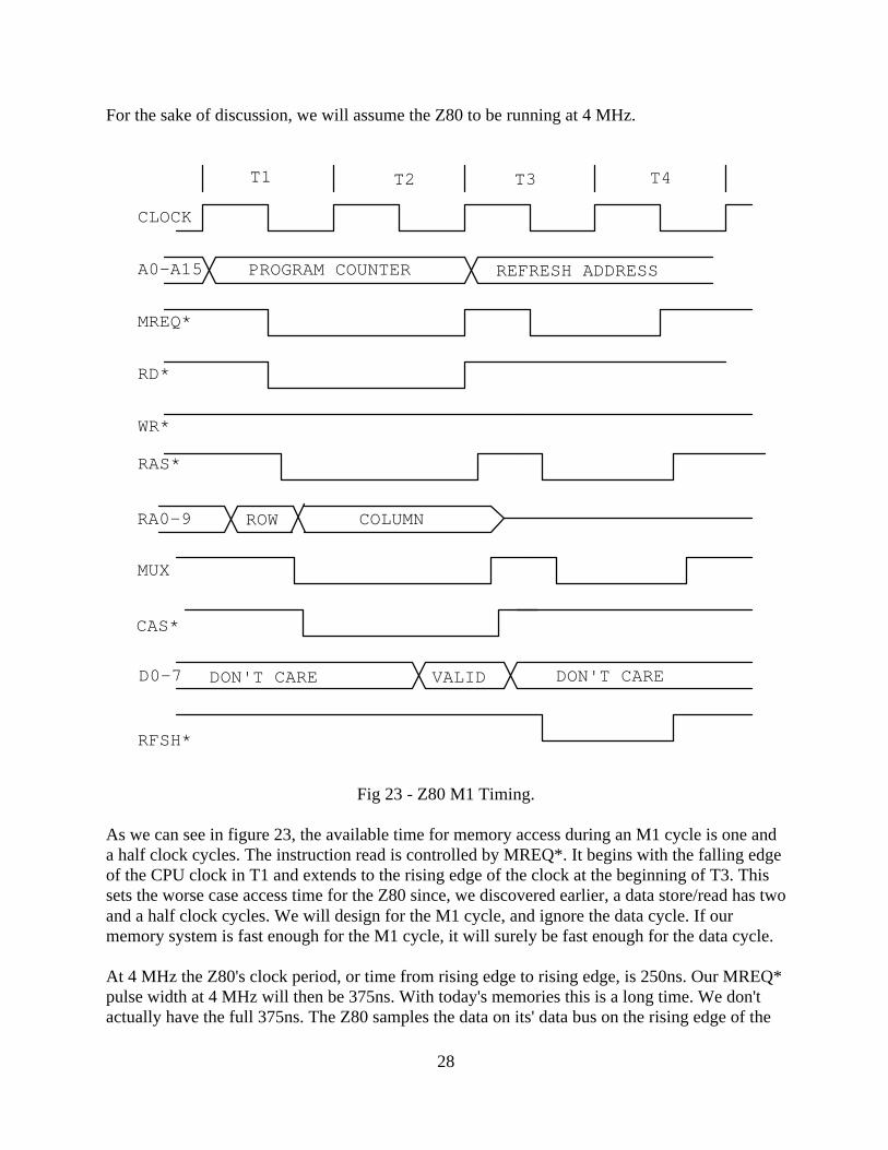
For the sake of discussion, we will assume the Z80 to be running at 4 MHz.
Fig 23 - Z80 M1 Timing.
As we can see in figure 23, the available time for memory access during an M1 cycle is one anda half clock cycles. The instruction read is controlled by MREQ*. It begins with the falling edgeof the CPU clock in T1 and extends to the rising edge of the clock at the beginning of T3. Thissets the worse case access time for the Z80 since, we discovered earlier, a data store/read has twoand a half clock cycles. We will design for the M1 cycle, and ignore the data cycle. If ourmemory system is fast enough for the M1 cycle, it will surely be fast enough for the data cycle.
At 4 MHz the Z80's clock period, or time from rising edge to rising edge, is 250ns. Our MREQ*pulse width at 4 MHz will then be 375ns. With today's memories this is a long time. We don'tactually have the full 375ns. The Z80 samples the data on its' data bus on the rising edge of the
CLOCK
A0-A15
MREQ*
RD*
RAS*
CAS*
MUX
WR*
VALIDD0-7
RA0-9 ROW COLUMN
RFSH*
DON'T CARE DON'T CARE
PROGRAM COUNTER REFRESH ADDRESS
T1 T2 T3 T4
28

clock. Data must be stable at the pins of the Z80 CPU chip some time before the rising edge ofthe clock to ensure that the Z80 reads correct data. In the case of the 4 MHz Z80 this time is35ns. Also, the Z80 may not make MREQ* active right on the falling clock edge. In the case ofthe 4 MHz Z80, it could be as long as 85ns after the clock. Since we have to design for the worstcase we must subtract 120ns (35+85) from our 375 ns. This still leaves us 255ns to accessmemory during the M1 cycle. We should be able to easily use 150ns DRAM parts with no waitstates with this design.
Notice also from figure 23 that the Z80 always follows the M1 memory fetch with a memoryrefresh cycle. This refresh cycle is technically part of the M1 cycle, using states T3 and T4. Ifthe Z80 didn't perform a refresh during this time the external bus would simply be idle. In doingthe refresh this way, Zilog gave us a no-penalty refresh. That is, refreshing the dram memoryuses no memory bandwidth that could have been used for something else. This a gift. You won'tsee it again. Modern processors utilize the full bandwidth for memory, and refresh must beforcibly inserted into the stream of accesses, thus taking some of the memory bandwidth forrefresh.
With the older memories, refresh would be implemented using RAS only refresh. All drams upto the 256K by 1 parts needed this, and some of the 256K parts did as well. If you're workingwith older parts, I.E. - 4K, 16K, 64K, you MUST implement RAS only refresh. If you are using256K parts, check the data sheet for the parts you intend to use before you begin. If they willsupport CAS before RAS refresh, then by all means that is the best way to do it. You willeliminate a lot of parts from the DRAM controller circuit, and a lot of the complexity in thecontrol logic for it.
29

APPLICATION DESIGNS
DISCLAIMER : The circuits described in this section are the authors best approximation of whatmight be successfully be implemented. For the most part, they have not been actually beenprototyped and made to run. Only circuit 5 has actualy been impemented. They are a compositeof designs done over the years which have been successful. They should be able to be built, butyou may discover some small errors in the schematics, or PAL equations, that will need to becorrected before they will run properly.
NOTE : Due to a bug in AmiPro which almost cost me this entire document, the schematics forthe application circuits will be included with this paper as separate postscript files.
OK. Enough theory. Let's get down to some actual circuits. In this section I will present someactual design attempts. We will start off with a simple design, easy to implement, then move onto more complex things.
30
CIRCUIT 1
Our first design attempt will be a Z80 running at 4 MHz, and having 64K of dynamic memory.We will provide an 8K EPROM for startup code. A CPU without I/O is worthless so we willalso provide an SIO to connect a serial terminal to.
As promised, circuit 1 is fairly simple. Page 1 of the schematics shows the Z80 CPU. It uses asimple RC network to generate RESET*. If I were to start adding "whistles and bells", the firstthing I would do is to generate RESET* with some kind of SCHMIDT TRIGGER gate. Thiswould eliminate the slow rise time in the RESET* signal.
The clock to the Z80, and its' peripheral chips, is generated by an oscillator module. Thetraditional clock driver circuit is replaced by a modern CMOS inverter; a 74HCT14.
RESET* is generated by an RC network feeding a section of a 74HCT14, a Schmidt triggerinverter. The resulting signal is inverted again to retain the active low polarity of the reset signal.
Also on page 1 is the EPROM. It is an 8K device, a 2764/27C64. It will ONLY be used duringstartup. We will see how this is implemented when we examine the PAL equations a little later.
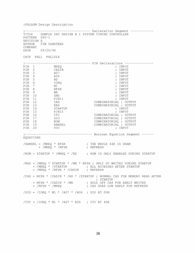
On page 2 we see the heart of the design, our DRAM controller. Since the Z80 can only address64K of memory I decided that we would give it that much; in two parts. The 4464 is a 64K by 4bit dram. Thus, two of these devices and we have a full 64KB of DRAM. That's not bad. It usedto take a fairly large board to do that.
The DRAM timing is generated by the PAL, at U5. The PAL chosen for this design is a 16L8.This device was chosen because they are cheap and easy to work with. Next to the PAL you willnotice a section of a D type flip-flop, U4. This is how we get the system started up.
When you power up the circuit, RESET* will go low for a time determined by the values of thecomponents in the RC circuit on page 1. When RESET* goes low, the Q output of U4B will gohigh (on page 2). This signal is feed to the PAL. In the PAL equations, it is called STARTUP,and it is active high. The full PAL listing is attached, but let's examine the equations in detail.
/ROM = STARTUP * /MREQ * /RD ; ROM IS ONLY ENABLED DURING STARTUP
The equation shown above illustrates how STARTUP is used to allow access to the ROM. Notethat ALL memory reads are directed to the ROM during startup. We didn't include any addresslines in the equations. The idea here is to copy the contents of the ROM into the DRAM, thenswitch the ROM out. EPROMs draw a considerable amount of power. By switching it out, andnot accessing it, the eprom will draw less power. Also, we simplify our memory control design.Since the Z80 can only address 64K of memory total, and we have 64K of DRAM plus 8K ofROM, we could have a sticky wicket indeed.
31
This eliminates that potential problem. Now we are fully flexible as to what we run in theDRAM. We would probably implement a monitor program to put in the ROM that would let usdownload other programs from a PC.
Continuing with our examination of the design for circuit 1, let's look at the DRAM controller.The entire DRAM circuit is presented on page 2 of the schematics. The address lines from theZ80 are multiplexed into the DRAM chips by the multiplexers at U7 and U9.
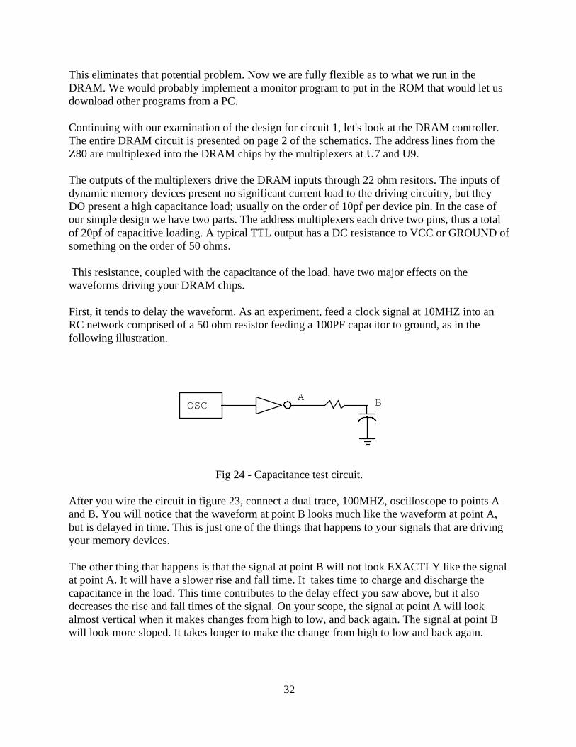
The outputs of the multiplexers drive the DRAM inputs through 22 ohm resitors. The inputs ofdynamic memory devices present no significant current load to the driving circuitry, but theyDO present a high capacitance load; usually on the order of 10pf per device pin. In the case ofour simple design we have two parts. The address multiplexers each drive two pins, thus a totalof 20pf of capacitive loading. A typical TTL output has a DC resistance to VCC or GROUND ofsomething on the order of 50 ohms.
This resistance, coupled with the capacitance of the load, have two major effects on thewaveforms driving your DRAM chips.
First, it tends to delay the waveform. As an experiment, feed a clock signal at 10MHZ into anRC network comprised of a 50 ohm resistor feeding a 100PF capacitor to ground, as in thefollowing illustration.
Fig 24 - Capacitance test circuit.
After you wire the circuit in figure 23, connect a dual trace, 100MHZ, oscilloscope to points Aand B. You will notice that the waveform at point B looks much like the waveform at point A,but is delayed in time. This is just one of the things that happens to your signals that are drivingyour memory devices.
The other thing that happens is that the signal at point B will not look EXACTLY like the signalat point A. It will have a slower rise and fall time. It takes time to charge and discharge thecapacitance in the load. This time contributes to the delay effect you saw above, but it alsodecreases the rise and fall times of the signal. On your scope, the signal at point A will lookalmost vertical when it makes changes from high to low, and back again. The signal at point Bwill look more sloped. It takes longer to make the change from high to low and back again.
OSCA B
32

Every time the signal changes state, it has to deal with that nasty capacitance again. On a low tohigh transition, the capacitance has to be charged. On a high to low transition it has to bedischarged.
Here, there is no substitute for brute force. In the schematic for circuit 1 you will notice that Idrew a 74157, not a 74LS157. This was not an accident. The 74157 has more drive capabilitythan its' 74LS157 equivalent. In making the "LS" line of TTL I.C.'s most manufacturers putresistors in series with the output transistors. This "softens" the output transitions. NOT what wewant to drive DRAMs with. If you can't find the plain 74157's, try the 74F157's. They have theresistors, but are speeded up so that they will generally work well.
In addition to having to deal with the delaying effect of the capacitance, and the slowing effect ithas on our waveforms, there is also ringing to worry about. At the speeds these signals transition(in excess of 100MHZ) we get a transmission line effect.
In addition to the RC we have that is formed by the resistance in the driver output, and thecapacitance of the load, now we have a coil introduced by the etch that connects the driver to thememory array, or worse, the wire-wrap wire.
As we all now from our basic electronics you can store energy in a coil. When we charge thecapacitance of our load, current flows in the coil. When the coil discharges a voltage is generatedin it that is the opposite polarity of that which charged it. The current generated is also out ofphase with the transition. Now we have a classic RF circuit.
The worst case for us is the high to low transition. The ringing generated by all of this can drivethe signal well below ground. Very few I.C.'s will really like this. In fact, it can destroy somedevices; especially older DRAM chips. When an input is taken below ground, the chip canbecome reverse biased, and "turn on" like an SCR. Like an SCR, when this happens, the onlyway to turn it back of is to remove power. For some devices there is no way you can removepower fast enough to prevent permanent damage, even if you knew that it had gone into SCRmode, which you probably won't. Usually the first indication you get is that awful smell ofburning I.C.'s. If you don't know what that smels like, good.
We will deal with ways to minimize this effect later, but, for now, let's just try to dampen it.That is the purpose of the 22 ohm resistors in series with the 74157 outputs. They are not inseries between VCC and the output transistor, so they don't effect our rise or fall times. Theirpurpose is to dampen the ringing on these lines.
For a memory array this small, they could have probably been left out. I included them here toteach proper design practices. Our goal here is not to save a few pennies on resistors, it is todesign something that actually has a chance to work.
To continue with the analysis of our design let's look at how the DRAM timing is generated.Consider the following equations with me.
/RAMSEL = /MREQ * RFSH ; THE WHOLE 64K IS DRAM
33
+ /MREQ * /RFSH ; REFRESH
To control DRAMs we need to generate RAS*, and CAS*. We also have to generate a signal tocontrol the multiplexers, the 74157's. The DRAM timing begins with MREQ* from the Z80.This indicates a memory access. The signal RAMSEL is generated from MREQ*. At first glanceit would seem that there is a redundant term in the equation for RAMSEL above. Did you catchit? RAMSEL is generated when RFSH is high, and when it is low. This would tend to say youcould eliminate the RFSH term from the equation, but you really can't. They don't both have thesame timing.
RAMSEL drives a delay line external to the PAL. Delay lines are very convenient to work with.This one would have 25ns between taps. This delay would satisfy most modern DRAM deviceswith access times of 150ns or afster. If you were trying to use slower devices then that you mighthave to chose different taps.
The first tap of the delay line is used to control the multiplexers. This signal is sometimes calledMUX.
The second tap is fed back into the PAL and used to generate DRAM timing. At this point, wehaven't really generated any DRAM timing, but all the players are in place. In the followingequations we will actually generate RAS and CAS.
/RAS = /MREQ * STARTUP * /WR * RFSH ; ONLY DO WRITES DURING STARTUP + /MREQ * /STARTUP * RFSH ; ALL ACCESSES AFTER STARTUP + /MREQ * /RFSH * /CASIN ; REFRESH
/CAS = RFSH * /CASIN * /RD * /STARTUP ; NORMAL CAS FOR MEMORY READAFTER ; STARTUP + RFSH * /CASIN * /WR ; HOLD OFF CAS FOR EARLY WRITES + /RFSH * /MREQ ; CAS GOES LOW EARLY FOR REFRESH
Whew! We finally did it. We got around to generating the memory timing. Did you catch it? Ok.We'll slow down and do it again. For a normal memory access we want to generate a RASsignal, followed by MUX, and finally CAS. We have a couple of special cases to think aboutthough. We have refresh to do, and our special case for startup. During startup we can write toDRAM memory, but we can't read it. Reads go to the ROM. How can this possibly be useful?Hopefully it will all make sense soon. Hang in there with me.
For a normal access we need to generate RAS first. This is generated from MREQ. If STARTUPis high we will only generate a RAS during a write. We can see this in the first term of the RASequation. After we get started up STARTUP will go low. From then on we use the second term.As long as RFSH is high we have a normal memory access. In this case RAS is basicallygenerated from MREQ. We'll cover refresh in a little bit.
34
To generate CAS we use the CAS equation. If STARTUP is high reads are blocked. Note in thefirst term of the CAS equation that STARTUP must be low during a read cycle. For a write CASis held off until WR goes active. We are using DRAM devices with common I/O pins, so weMUST implement early write. Holding off CAS until WR goes active does this for us. WR fromthe Z80 goes directly to the memory array. When CAS is generated there will be a delay of onePAL propagation time between when WR goes low, and when CAS will go low. This satisfiesthe setup time requirement on the DRAMs WE pin.
To complete the startup of our design we need a small piece of code. Consider the following.;; STARTUP CODE FOR CIRCUIT 1;
ORG 0 ; THE Z80 GOES HERE ON RESET;START: LD DE, 0 ; DESTINATION ADDRESS
LD HL, 0 ; SOURCE ADDRESSLD BC, 2000H ; LENGTHLDIR ; COPY ITOUT (0FFH), A ; KICK OUT THE ROM
The above code listing is a very simple way to get our little Z80 started up. At RESET* theflip-flop at U4B was set presenting the signal STARTUP to the PAL. In this mode we can readfrom the ROM and write to the DRAM. The startup code simply copies code starting at zero inmemory, to zero in memory, for the length of the rom. Thus. every rom location will be read,then written to the same address in the DRAM. Finally, an output instruction was executed toswitch the rom out. Note that IORQ* is tied to the clear pin of U4B. When the output instructionis executed it pulses the flip-flop.
The next instruction will be fetched from the DRAM. STARTUP will be low, and that willsatisfy the RAS equation in the PAL. From now until the next RESET* the Z80 will run fromDRAM.
Now all we have to do is keep the DRAM refreshed. The Z80 was designed to refresh dynamicmemories. Unfortunately that was almost 20 years ago, and the popular DRAM then was 16K by1. The Z80 doesn't provide enough address bits to refresh modern DRAMS using RAS onlyrefresh. So, what do we do. Well, all is not lost. We can use the refresh signal from the Z80 totrigger our refresh, but not to use the Z80's refresh address. That will work.
As we learned earlier, there are two ways to refresh dynamic memory; RAS only, and CASbefore RAS. The Z80 was designed to work with RAS only refresh. This is not too surprising asthat was all we had back then. The DRAM chip I chose for this design will support CAS beforeRAS refresh. Whenever possible we should use this because it reduces the parts count andcomplexity of our design.
The CAS before RAS refresh is all handled inside our PAL. Let's look at those equations again.
35
/RAS = . . . . . . . .
+ /MREQ * /RFSH * /CASIN ; REFRESH
/CAS = . . . . . . . .
+ /RFSH * /MREQ ; CAS GOES LOW EARLY FOR REFRESH
Above we see only the refresh portions of the RAS and CAS equations. When the Z80 wants todo a refresh it will signal this by asserting (taking low) both MREQ* and RFSH*. When we seethis look what happens. CAS is generated from MREQ* instead of RAS. RAS is generated fromCASIN, which comes from the second tap on the delay line. That's all there is to it. Done.
CAS will go low first, then RAS. The multiplexers will switch when MUX changes, but wedon't care. When CAS goes low first the DRAM ignores what is on its address pins. Refresh isfully taken care of.
We have spent quite a lot of time on page 2 of the design because that is where the DRAMtiming gets handled, and this paper IS about doing just that; interfacing DRAMS to the Z80.
On page 3 we see the implementation of our SIO. It turns out that using the SIO means that weneed a CTC as well. After all, we need something to generate baud rate clocks for the SIO don'twe?
Simple chip select signals are generated for these devices in the PAL. The Z80 address lines arenot fully decoded to save pins on the PAL. The equations for these chip selects are as follows.
/SIO = /IORQ * M1 * /A07 * /A06 ; SIO AT 00H
/CTC = /IORQ * M1 * /A07 * A06 ; CTC AT 40H
Pretty simple huh? Can you tell me why I included M1* in these equations? You would seesome very strange things happening if you didn't; just about the time you started to use theinterrupt capabilities of the SIO or the CTC. The Z80 signals an interrupt acknowledge byexecuting a bus cycle with both M1* and IORQ* low. This is normally a mutually exclusivecondition. M1 signals an instruction fetch cycle while IORQ signals an I/O cycle. When they golow together it is an interrupt acknowledge cycle.
The Z80 peripheral chips decode this internally and place their interrupt vector on the bus.Blocking the chip select prevents a spurious write to one of the chips registers, or to another I/Odevice you may wire into the circuit.
Z80 interrupts are wired in our sample circuit. The INT pin of both the CTC and the SIO areconnected to the INT pin of the Z80. There is a 10K pullup on this line. The INT pins of all the
36
Z80 family parts are open drain. That means they can pull the line low, but they can't force ithigh. This allows a daisy chain structure to work.
The interrupts are prioritized by the way the enable pins of the peripheral chips are wired. Notethat the SIO has its' IEI, or Interrupt Enable In pin, tied high. That makes it the highest prioritydevice in the interrupt chain. The IEO, or Interrupt Enable Out, pin from the SIO is connected tothe IEI pin of the CTC. If there were another device, a PIO for example, the IEO from the CTCwould go to the IEI of the PIO.
There is a limit to how far this can be carried. You can only connect four devices in this manner.It takes time for the enables to trickle down the chain and it has to be complete early in theinterrupt acknowledge cycle. Then the correct will be able to place its' vector on the bus at theright time.
This concludes our analysis of circuit 1. We have implemented a simple Z80 with 64K ofDRAM. To make the circuit more useful you would probably want to add some more I/O to it.
37
;PALASM Design Description
;---------------------------------- Declaration Segment ------------TITLE SAMPLE Z80 DESIGN # 1 SYSTEM TIMING CONTROLLERPATTERN Z80-1REVISION AAUTHOR TIM OLMSTEADCOMPANY DATE 09/20/96
CHIP PAL1 PAL16L8
;---------------------------------- PIN Declarations ---------------PIN 1 MREQ ; INPUT PIN 2 CASIN ; INPUT PIN 3 A07 ; INPUT PIN 4 A06 ; INPUT PIN 5 RD ; INPUT PIN 6 IORQ ; INPUT PIN 7 M1 ; INPUT PIN 8 RFSH ; INPUT PIN 9 WR ; INPUT PIN 10 GND ; INPUT PIN 11 PIN11 ; INPUT PIN 12 CAS COMBINATORIAL ; OUTPUTPIN 13 RAS COMBINATORIAL ; OUTPUTPIN 14 STARTUP ; INPUT PIN 15 PIN15 ; INPUT PIN 16 CTC COMBINATORIAL ; OUTPUTPIN 17 SIO COMBINATORIAL ; OUTPUTPIN 18 ROM COMBINATORIAL ; OUTPUTPIN 19 RAMSEL COMBINATORIAL ; OUTPUTPIN 20 VCC ; INPUT
;----------------------------------- Boolean Equation Segment ------EQUATIONS
/RAMSEL = /MREQ * RFSH ; THE WHOLE 64K IS DRAM + /MREQ * /RFSH ; REFRESH
/ROM = STARTUP * /MREQ * /RD ; ROM IS ONLY ENABLED DURING STARTUP
/RAS = /MREQ * STARTUP * /WR * RFSH ; ONLY DO WRITES DURING STARTUP + /MREQ * /STARTUP ; ALL ACCESSES AFTER STARTUP + /MREQ * /RFSH * /CASIN ; REFRESH
/CAS = RFSH * /CASIN * /RD * /STARTUP ; NORMAL CAS FOR MEMORY READ AFTER ; STARTUP + RFSH * /CASIN * /WR ; HOLD OFF CAS FOR EARLY WRITES + /RFSH * /MREQ ; CAS GOES LOW EARLY FOR REFRESH
/SIO = /IORQ * M1 * /A07 * /A06 ; SIO AT 00H
/CTC = /IORQ * M1 * /A07 * A06 ; CTC AT 40H
38
CIRCUIT 2
Our second design attempt will be a Z80 running at 4 MHz, and having 64K of dynamicmemory. It is essentially the same as the first example except that we replaced the nice, easy touse, DRAM devices with some older 64K by 1 parts. These devices require RAS ONLY refresh.We will use the refresh facility built into the Z80 CPU to perform this refresh for us. Since thatis the only difference, we will not go through describing the other portions again. Instead we willconcentrate on the differences.
On page 2 we see the heart of the design, our DRAM controller. It LOOKS just like the one inour first example, but it isn't. Examine the 74157 multiplexer inputs carefully, and compare themto the first example.
In example 1 we connected A00 through A07 to the "A" inputs of the multiplexes. In the secondexample we connected A00 through A07 to the "B" inputs. Why would we do that?
In the first design example we were implementing CAS before RAS refresh, so the exactordering of the address lines was not important. In this example we are implementing RASONLY refresh. As stated above, we want to use the refresh facility designed into the Z80 CPUchip to do this. After all, why should we make life any harder on us than it has to be? It turns outthat the devices selected in this design example, a HITACHI 4864, can be refreshed in 128accesses. This will work with what the Z80 provides.
During a refresh cycle the Z80 outputs the refresh address on its' A00 through A06 address pins.This address needs to be allowed to flow through the multiplexers and be presented to theDRAM chips. If we examine page 2 of the schematic we will discover that the select pin of themultiplexers is high before RAS occurs. We can confirm this by examining the PAL equationsfor RAMSEL and RAS.
/RAMSEL = /MREQ * RFSH ; THE WHOLE 64K IS DRAM
/RAS = /MREQ * STARTUP * /WR * RFSH ; ONLY DO WRITES DURING STARTUP + /MREQ * /STARTUP * RFSH ; ALL ACCESSES AFTER STARTUP + /MREQ * /RFSH ; REFRESH IS RAS ONLY
Note that RAMSEL and RAS effectively have the same equation after STARTUP goes low;whenever MREQ goes active, they do too, except for during refresh. If we examine page 2 of theschematic we find that the multiplexer control signal comes from the first tap of the delay line. Itwill go low one time delay AFTER RAMSEL does. Therefore, at the time RAMSEL, and RAS,goes low, the control signal will be high.
During refresh we want to have the Z80's A00 through A06 used as row addresses, and thus therefresh address. To do this then, we have to connect them to the "B" inputs of the multiplexers.
Another difference in the dynamic memory design of circuit 2 is the memory chips themselves.The parts selected for this design have separate input and output pins. You can see the memory
39
devices on page 3 of the schematics. Since these devices have separate I/O pins I decided toimplement them that way. I could have tied the two pins together, and used the same controllogic I did on the last design, but I decided that I would do it differently.
When implementing the separate I/O pin design, a 74LS244 is used to connect the data out pinto the Z80's data bus when needed. The PAL on page 2 generates a signal, EN245, to do this. Itis only enabled for memory reads after STARTUP goes low. For writes, EN245 remains high,and the 74LS244 is disabled.
What does this buy us? Where is the advantage in this approach? What it buys us is speed onwrites. Since we don't have to do early writes, we can generate the same timing for reads and forwrites. The Z80 will pulse WR* late in the bus cycle to strobe the data into the memories.
The DRAMs see this as a read-modify-write cycle. After RAS and CAS have been cycled, thememory device will access the location specified, and present that data to its' output pin. Thisdoesn't cause any problem because the 74LS244 is disabled. Later the Z80 places data to bewritten on the data bus, and pulses the WR* pin. No problem. The memory device accepts thedata and writes it to the same location. The output pins will continue to have the data originallystored in the specified location.
By being able to cycle RAS and CAS earlier in the memory cycle, the memory system accessesfaster. This may not make much difference with a Z80 running at 4 MHZ, but it might at 10MHZ. I once ran a Z8001 at 10 MHZ with 150 ns DRAMS using this technique, and no waitstates. It ONLY works with dynamic ram devices with separate I/O pins, but it is worthremembering if you ever have the occasion to be working with these parts.
Another difference between this design example, and the first one, is visible on page 2 of theschematics. The WE* pin of the DRAMs is driven by WR* still, but WR* is buffered by twostages of a 74F04. This double inversion results in the same signal polarity as WR*, but doesn'tload the WR* pin as much as it would if we didn't buffer it. The extra delay of the two inverterstages is negligible in this design.
The memory array in this design is bigger than the first example since we have eight devicesinstead of two. This means more capacitance. The HITACHI data book, from which these devices were selected says that the RAS, CAS, and WE pins are 10pf, while all others are 7pf.At 10pf the load on RAS, CAS, and WE is now 80pf. The load on the address lines, and datalines, is 56pf. This is not bad, but it is becoming noticeable. This is why we buffered andterminated the WE driver.
40
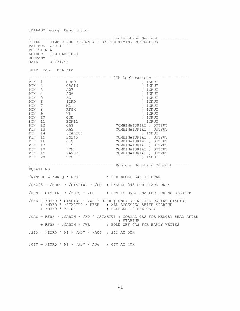
;PALASM Design Description
;---------------------------------- Declaration Segment ------------TITLE SAMPLE Z80 DESIGN # 2 SYSTEM TIMING CONTROLLERPATTERN Z80-1REVISION AAUTHOR TIM OLMSTEADCOMPANY DATE 09/21/96
CHIP PAL1 PAL16L8
;---------------------------------- PIN Declarations ---------------PIN 1 MREQ ; INPUT PIN 2 CASIN ; INPUT PIN 3 A07 ; INPUT PIN 4 A06 ; INPUT PIN 5 RD ; INPUT PIN 6 IORQ ; INPUT PIN 7 M1 ; INPUT PIN 8 RFSH ; INPUT PIN 9 WR ; INPUT PIN 10 GND ; INPUT PIN 11 PIN11 ; INPUT PIN 12 CAS COMBINATORIAL ; OUTPUTPIN 13 RAS COMBINATORIAL ; OUTPUTPIN 14 STARTUP ; INPUT PIN 15 EN245 COMBINATORIAL ; OUTPUTPIN 16 CTC COMBINATORIAL ; OUTPUTPIN 17 SIO COMBINATORIAL ; OUTPUTPIN 18 ROM COMBINATORIAL ; OUTPUTPIN 19 RAMSEL COMBINATORIAL ; OUTPUTPIN 20 VCC ; INPUT
;----------------------------------- Boolean Equation Segment ------EQUATIONS
/RAMSEL = /MREQ * RFSH ; THE WHOLE 64K IS DRAM
/EN245 = /MREQ * /STARTUP * /RD ; ENABLE 245 FOR READS ONLY
/ROM = STARTUP * /MREQ * /RD ; ROM IS ONLY ENABLED DURING STARTUP
/RAS = /MREQ * STARTUP * /WR * RFSH ; ONLY DO WRITES DURING STARTUP + /MREQ * /STARTUP * RFSH ; ALL ACCESSES AFTER STARTUP + /MREQ * /RFSH ; REFRESH IS RAS ONLY
/CAS = RFSH * /CASIN * /RD * /STARTUP ; NORMAL CAS FOR MEMORY READ AFTER ; STARTUP + RFSH * /CASIN * /WR ; HOLD OFF CAS FOR EARLY WRITES
/SIO = /IORQ * M1 * /A07 * /A06 ; SIO AT 00H
/CTC = /IORQ * M1 * /A07 * A06 ; CTC AT 40H
41
CIRCUIT 3
Our third design attempt will again be a Z80 running at 4 MHz, and having 64K of dynamicmemory. It is the same as the second example except that we have implemented the RAS ONLYrefresh the hard way. This example is really for the reader who may NOT be using a Zilogprocessor. It would be hard to justify using external refresh counters, and the extra level ofmultiplexers, for a Zilog processor. The Z80, Z180, Z280, Z380, and Z8000 all have refreshcapabilities.
Again on page 2 we see the heart of the DRAM design. This time it looks quite different. Thefirst thing we notice is a second level of multipexers. Our normal address multiplexers feed asecond set of 74157's. These new multiplexers are configured to normally pass the data on their"B" inputs through. This will present the normal addresses to the memories. The select pins ofthese new multiplexers is driven by RFSH* from the Z80. During a refresh cycle this signal willgo low, and select the "A" inouts of the multiplexers. This gates the outputs of an eight bitcounter through to the DRAMs.
The 74LS393 counter is incremented on the high to low transition of its' clock, so RFSH isinverted to drive the first section. The counter is incremented at the end of the refresh cycle. Itwill continue to increment for every refresh cycle. This will meet the needs of our dynamicmemories. To refresh larger memories you would need more bits on the counter, and widermultiplexers.
NOTE : The PAL listing for this design is included for completeness, but it is identical to designexample 2.
42

;PALASM Design Description
;---------------------------------- Declaration Segment ------------TITLE SAMPLE Z80 DESIGN # 3 SYSTEM TIMING CONTROLLERPATTERN Z80-1REVISION AAUTHOR TIM OLMSTEADCOMPANY DATE 09/21/96
CHIP PAL1 PAL16L8
;---------------------------------- PIN Declarations ---------------PIN 1 MREQ ; INPUT PIN 2 CASIN ; INPUT PIN 3 A07 ; INPUT PIN 4 A06 ; INPUT PIN 5 RD ; INPUT PIN 6 IORQ ; INPUT PIN 7 M1 ; INPUT PIN 8 RFSH ; INPUT PIN 9 WR ; INPUT PIN 10 GND ; INPUT PIN 11 PIN11 ; INPUT PIN 12 CAS COMBINATORIAL ; OUTPUTPIN 13 RAS COMBINATORIAL ; OUTPUTPIN 14 STARTUP ; INPUT PIN 15 EN245 COMBINATORIAL ; OUTPUTPIN 16 CTC COMBINATORIAL ; OUTPUTPIN 17 SIO COMBINATORIAL ; OUTPUTPIN 18 ROM COMBINATORIAL ; OUTPUTPIN 19 RAMSEL COMBINATORIAL ; OUTPUTPIN 20 VCC ; INPUT
;----------------------------------- Boolean Equation Segment ------EQUATIONS
/RAMSEL = /MREQ * RFSH ; THE WHOLE 64K IS DRAM
/EN245 = /MREQ * /STARTUP * /RD ; ENABLE 245 FOR READS ONLY
/ROM = STARTUP * /MREQ * /RD ; ROM IS ONLY ENABLED DURING STARTUP
/RAS = /MREQ * STARTUP * /WR * RFSH ; ONLY DO WRITES DURING STARTUP + /MREQ * /STARTUP * RFSH ; ALL ACCESSES AFTER STARTUP + /MREQ * /RFSH ; REFRESH IS RAS ONLY
/CAS = RFSH * /CASIN * /RD * /STARTUP ; NORMAL CAS FOR MEMORY READ AFTER ; STARTUP + RFSH * /CASIN * /WR ; HOLD OFF CAS FOR EARLY WRITES
/SIO = /IORQ * M1 * /A07 * /A06 ; SIO AT 00H
/CTC = /IORQ * M1 * /A07 * A06 ; CTC AT 40H
43
CIRCUIT 4
For our next design example we will make things a little harder for ourselves. The goal of thisexample is to allow the Z80 to address 1MB of memory. The Z80 microprocessor can onlyaddress up to 64K of memory. Well, at least at any one moment in time, that is.
What we need is an MMU, or Memory Management Unit. Modern processors, such as the Intel80386/486/etc, all have MMUs built into the CPU chips. The Z80 doesn't have one. Severaltechniques have been developed over the years to perform this function. Some are probablybetter than others. My favorite is the one described in some detail earlier. We will implementthis MMU in hardware on this example design.
When we are done, we will have an MMU which will map memory in 4K pages. This is anadequate size for our use, It balances page granularity with hardware, and software, complexity.A TTL chip exists that will allow us to achieve this goal in two parts. Look at page 1 of theschematics for this design. You will immediately notice that two 74LS189's have been added inthe upper right corner of the page. Note also that the Z80 address lines 12 through 15 have newnames. They are called ZA12 to ZA15, and they go directly to the 74LS189's. The 74LS189 is a16 by 4 register file. It is a TTL device, so it is fast. We will not need to insert any delays in thememory cycle to accommodate the MMU we are building.
The data input pins of the 74LS189's are connected to the Z80's data bus. The MMU is written toby a Z80 OUT (C), A instruction. It is important to note that this is the only form of the outputinstruction that we can use to write to the MMU. When the Z80 executes the OUT (C), Ainstruction it places the contents of the BC register pair on the address pins. The contents of theC register will appear on the lower half of the address bus, that is A00 through A07. Thecontents of the B register will be placed on the upper half of the address bus, that is A08 throughA15. We will need to place the address of the MMU register to be written in the upper four bitsof the B register. This will then be placed on ZA12 through ZA15, and select the proper registerfor us.
We could not use the OUT (##), A because the Z80 places the contents of the A register on theupper half of the address bus during the actual I/O instruction. We can't use the OTIR/OTDRinstruction because these instructions want to decrement the B register after each execution.
This MMU approach was discussed in great detail earlier, but we will review the CPU startupsequence here in order to relate it to the hardware. There are a couple of other subtle differencesin this design. Note, also on page 1, that the EPROM uses ZA12 instead of A12. This is becausewe must be able to execute from the ROM at startup because the MMU comes up with alllocations undefined.
On page 2 of the schematics you will see our familiar STARTUP flip-flop. But wait. It is notquite the same as in our previous examples. We need to use I/O instructions to initialize theMMU so we don't dare reset the flip-flop on the first IORQ. Instead we will use something morespecific, that can also afford to wait until after the MMU is up; the SIO. The SIO can be
44
initialized anytime after the MMU is initialized. When we do this, the flip-flop will be cleared,and the ROM switched out. We are then running from our DRAM.
You will notice that the DRAM used in this example is a 1MB, 30 pin SIMM. This memoryrequires two more multiplexed address lines than the 64K designs we have been working with.To accommodate this we have added another 74157 multiplexer, at U9. Our MMU generates 20address lines, just enough to support 1MB of memory. Therefore, we use them all on themultiplexers. The PAL equations for this design are the same as for example one, except that weneed to generate an I/O chip select for the MMU.
Since the SIMM module uses common I/O pins we must implement early write. We will alsoimplement CAS before RAS refresh. This makes our design very clean. Compare page 2 of ourschematics with example 3. This is much better.
The rest of the design is identical to our previous examples.
45
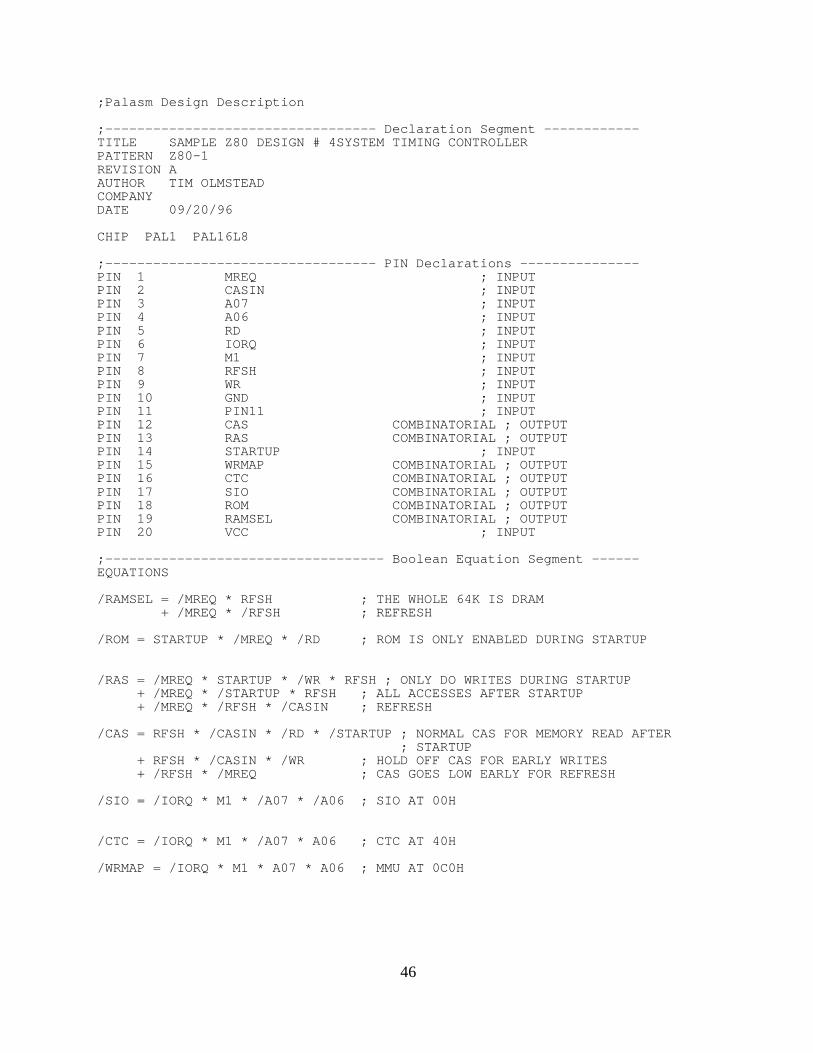
;Palasm Design Description
;---------------------------------- Declaration Segment ------------TITLE SAMPLE Z80 DESIGN # 4SYSTEM TIMING CONTROLLERPATTERN Z80-1REVISION AAUTHOR TIM OLMSTEADCOMPANY DATE 09/20/96
CHIP PAL1 PAL16L8
;---------------------------------- PIN Declarations ---------------PIN 1 MREQ ; INPUT PIN 2 CASIN ; INPUT PIN 3 A07 ; INPUT PIN 4 A06 ; INPUT PIN 5 RD ; INPUT PIN 6 IORQ ; INPUT PIN 7 M1 ; INPUT PIN 8 RFSH ; INPUT PIN 9 WR ; INPUT PIN 10 GND ; INPUT PIN 11 PIN11 ; INPUT PIN 12 CAS COMBINATORIAL ; OUTPUTPIN 13 RAS COMBINATORIAL ; OUTPUTPIN 14 STARTUP ; INPUT PIN 15 WRMAP COMBINATORIAL ; OUTPUTPIN 16 CTC COMBINATORIAL ; OUTPUTPIN 17 SIO COMBINATORIAL ; OUTPUTPIN 18 ROM COMBINATORIAL ; OUTPUTPIN 19 RAMSEL COMBINATORIAL ; OUTPUTPIN 20 VCC ; INPUT
;----------------------------------- Boolean Equation Segment ------EQUATIONS
/RAMSEL = /MREQ * RFSH ; THE WHOLE 64K IS DRAM + /MREQ * /RFSH ; REFRESH
/ROM = STARTUP * /MREQ * /RD ; ROM IS ONLY ENABLED DURING STARTUP
/RAS = /MREQ * STARTUP * /WR * RFSH ; ONLY DO WRITES DURING STARTUP + /MREQ * /STARTUP * RFSH ; ALL ACCESSES AFTER STARTUP + /MREQ * /RFSH * /CASIN ; REFRESH
/CAS = RFSH * /CASIN * /RD * /STARTUP ; NORMAL CAS FOR MEMORY READ AFTER ; STARTUP + RFSH * /CASIN * /WR ; HOLD OFF CAS FOR EARLY WRITES + /RFSH * /MREQ ; CAS GOES LOW EARLY FOR REFRESH
/SIO = /IORQ * M1 * /A07 * /A06 ; SIO AT 00H
/CTC = /IORQ * M1 * /A07 * A06 ; CTC AT 40H
/WRMAP = /IORQ * M1 * A07 * A06 ; MMU AT 0C0H
46
CIRCUIT 5
Our last design example is a surprise. We have only discussed the Z80 CPU thus far in thispaper, but there exist some descendants of the Z80. One of these is the Z180. Originallydeveloped by HITACHI, as the 64B180, Zilog now sells this processor as the Z180. HITACHIhad some problems with early versions of this chip when connected to Z80 peripheral chips. TheZilog parts have this fixed, as do current production HITACHI parts.
Another Z80 successor chip is the Z280, which is depicted in this design. This processor has anumber of peripheral devices built into it. It has three counter/timer channels, four DMAchannels, and a UART. This design uses one of the counter inputs to clock the UART.
NOTE : This design example has been successfully implemented. Some of the features of thisdesign do not exist in our previous examples. For example, this design has 32K of staticmemory, and a Z80 PIO chip. I elected not to remove them so as to preserve the fact that this is arunning design.
The actual baud rate clock is generated external to the Z280 as the counter has some funnycharacteristics, when counting an external signal, that make it undesirable for use as a baud rategenerator. If the processor clock were to be selected to be a nice multiple of a baud ratefrequency, the counter can divide the CPU clock and generate baud clocks.
The Z280 is a multiplexed address/data bus processor. Further, it can be implemented with eitheran 8 bit, or 16 bit, data bus. It this example I have chosen to implement the 8 bit data bus. In thismode the Z280 is most like its' cousin, the Z80. A single 74LS373, at U5, is used to de-mux thelower 8 bits of the address from the data bus.
The circuit at the top of page 1 is required to get the CPU started up. There are several bits in theBTI, or Bus Timing and Initialization, register that can only be set in this way. The hardware reset signal from the RC network is connected to a 74LS14, which is a SCHMIDT TRIGGERinverter. This gate will clean up the slow rise time from the RC network and give us a TTLtransition. It is inverted again by another section of the 74LS14 to restore the negative true logic.This signal goes to the data inputs of a 74LS164, a shift register. The shift register is constantlyclocked by the output clock of the Z280. Five clocks after the data input of the shift registerwent low, RESET* and STARTUP* will both be low.
The input pulse from the 74LS14 will be on the order of 47ms; a 4.7k pullup and a 100uf cap.When this times out the data input of the shift register will go high. This begins the startupsequence of the Z280. Two clocks later RESET* goes high. Note that the signal STARTUP* isconnected to the WAIT* pin of the Z280. When the Z280 comes out of RESET it samplesWAIT. If it is low, the data is sampled from the data bus and loaded into the BTI register. Theshift register holds STARTUP* low for two clocks after RESET* goes high, then STARTUP*goes high. This circuit then sits idle until the next power up, or manual reset.
47
On page 2 of the schematics we see the EPROM, static ram, Z80 PIO, and the serial I/O driversand receivers. The Z280 has a serial port built into it so an SIO chip wasn't necessary for thisdesign.
On page 3 of the schematics we see the DRAM controller. It looks just about like our last designexcept that the STARTUP flip-flop is gone. It is not needed. The Z280 has enough address spacefor everything. The PAL directly generates chip selects for everything. Note that the SIMMsocket is wired for a 4MB SIMM. This is the biggest SIMM that will fit into a 30 pin module,and it fits nicely into the Z280's address space.
48
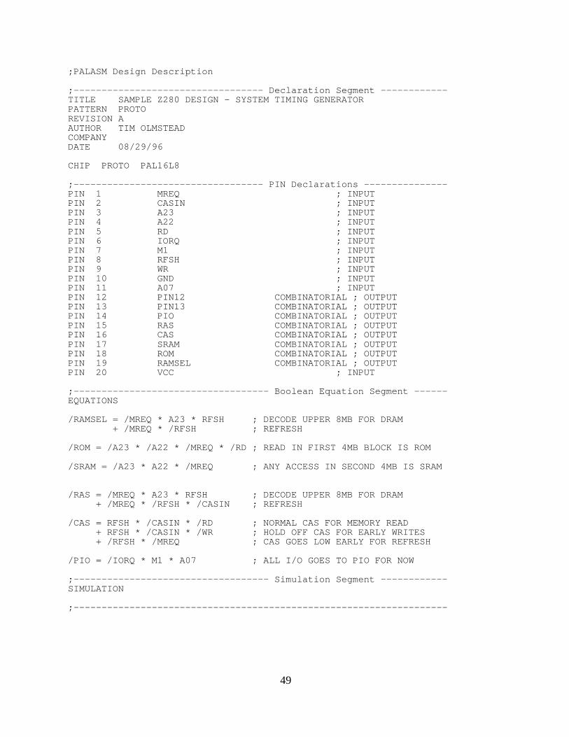
;PALASM Design Description
;---------------------------------- Declaration Segment ------------TITLE SAMPLE Z280 DESIGN - SYSTEM TIMING GENERATORPATTERN PROTOREVISION AAUTHOR TIM OLMSTEADCOMPANY DATE 08/29/96
CHIP PROTO PAL16L8
;---------------------------------- PIN Declarations ---------------PIN 1 MREQ ; INPUT PIN 2 CASIN ; INPUT PIN 3 A23 ; INPUT PIN 4 A22 ; INPUT PIN 5 RD ; INPUT PIN 6 IORQ ; INPUT PIN 7 M1 ; INPUT PIN 8 RFSH ; INPUT PIN 9 WR ; INPUT PIN 10 GND ; INPUT PIN 11 A07 ; INPUTPIN 12 PIN12 COMBINATORIAL ; OUTPUTPIN 13 PIN13 COMBINATORIAL ; OUTPUTPIN 14 PIO COMBINATORIAL ; OUTPUTPIN 15 RAS COMBINATORIAL ; OUTPUTPIN 16 CAS COMBINATORIAL ; OUTPUTPIN 17 SRAM COMBINATORIAL ; OUTPUTPIN 18 ROM COMBINATORIAL ; OUTPUTPIN 19 RAMSEL COMBINATORIAL ; OUTPUTPIN 20 VCC ; INPUT
;----------------------------------- Boolean Equation Segment ------EQUATIONS
/RAMSEL = /MREQ * A23 * RFSH ; DECODE UPPER 8MB FOR DRAM + /MREQ * /RFSH ; REFRESH
/ROM = /A23 * /A22 * /MREQ * /RD ; READ IN FIRST 4MB BLOCK IS ROM
/SRAM = /A23 * A22 * /MREQ ; ANY ACCESS IN SECOND 4MB IS SRAM
/RAS = /MREQ * A23 * RFSH ; DECODE UPPER 8MB FOR DRAM + /MREQ * /RFSH * /CASIN ; REFRESH
/CAS = RFSH * /CASIN * /RD ; NORMAL CAS FOR MEMORY READ + RFSH * /CASIN * /WR ; HOLD OFF CAS FOR EARLY WRITES + /RFSH * /MREQ ; CAS GOES LOW EARLY FOR REFRESH
/PIO = /IORQ * M1 * A07 ; ALL I/O GOES TO PIO FOR NOW
;----------------------------------- Simulation Segment ------------SIMULATION
;-------------------------------------------------------------------
49

APPLICATION SUMMARY
In this section we have examined several example designs for different configurations ofdynamic memory as interfaced to Zilog Z80 processors, and their descendants. It is hoped thatthis "hands on" approach will lead to a greater understanding of how to implement dynamicmemories in your projects.
If you are not interested in Zilog processors then you must extract what you need from thisdocument and apply it to your choice of processors. Some of them can be quite a challenge.
After awhile these DRAM controller designs begin to look pretty familiar, and not nearly soscary. We have already covered many facets of the design. In the next section, we will examinedesign considerations for laying out a PCB, or worse yet, hand wiring.
50
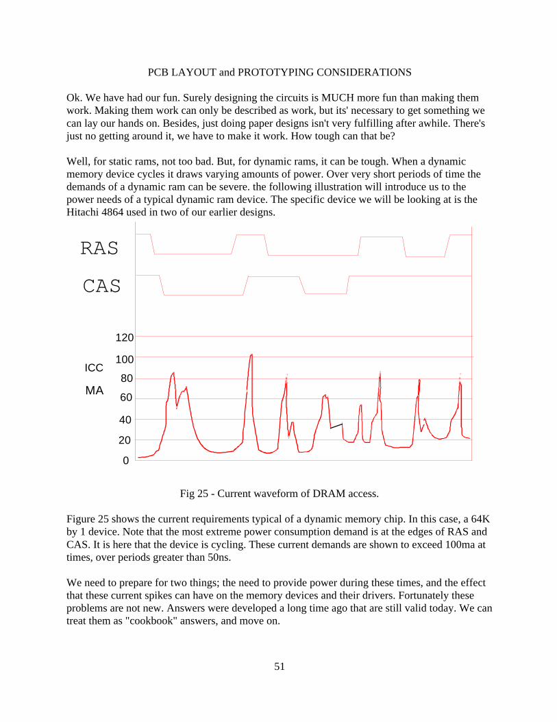
PCB LAYOUT and PROTOTYPING CONSIDERATIONS
Ok. We have had our fun. Surely designing the circuits is MUCH more fun than making themwork. Making them work can only be described as work, but its' necessary to get something wecan lay our hands on. Besides, just doing paper designs isn't very fulfilling after awhile. There'sjust no getting around it, we have to make it work. How tough can that be?
Well, for static rams, not too bad. But, for dynamic rams, it can be tough. When a dynamicmemory device cycles it draws varying amounts of power. Over very short periods of time thedemands of a dynamic ram can be severe. the following illustration will introduce us to thepower needs of a typical dynamic ram device. The specific device we will be looking at is theHitachi 4864 used in two of our earlier designs.
Fig 25 - Current waveform of DRAM access.
Figure 25 shows the current requirements typical of a dynamic memory chip. In this case, a 64Kby 1 device. Note that the most extreme power consumption demand is at the edges of RAS andCAS. It is here that the device is cycling. These current demands are shown to exceed 100ma attimes, over periods greater than 50ns.
We need to prepare for two things; the need to provide power during these times, and the effectthat these current spikes can have on the memory devices and their drivers. Fortunately theseproblems are not new. Answers were developed a long time ago that are still valid today. We cantreat them as "cookbook" answers, and move on.
RAS
CAS
100
120
80
60
40
20
0
ICC
MA
51
The current demands can be met by adding capacitors near each DRAM device. There should bea .1-.33 uf cap across every dynamic memory in the design. When you are using SIMM, you canforget this. There are already capacitors under the DRAM chips on the SIMM PCB. You can't doany better than this, so don't try.
For designs like our first three, you should locate a bypass capacitor physically near eachmemory device. The traces connecting the capacitors to the memory devices should go directlyto the power pins of the DRAM chip, and be as heavy as possible; fifty thousandths at LEAST.It is these capacitors that will provide the instantaneous current that the circuit demands. If youare hand wiring your circuit, lay the capacitor across the package and solder the leads directly tothe power pins of the memory chip. Remember. One for each chip. Don't skip any.
For older technology DRAMS, up to 64K, you should use .1uf capacitors. From 256K and up,you should use .33uf. These devices require even more current than their predessors.
In addition to the bypass capacitors you should provide solid tantalum capacitors located nearthe memory array. These tantalum capacitors should be 4.7uf to 10uf. For a small memory arrayI would prefer 10uf. For a large array I would prefer 4.7uf. This would spread the capacitancearound the array.
The .1uf, or .33uf, capacitors will provide the current needed by the DRAMs when they arecycling but they need to be recharged between current spikes. The solid tantalum electrolyticswill do this. You may use either the axial lead rolled tantalum capacitors, or the dipped tantalumcapacitors.
How many electrolytic capacitors you will need is a function of how many DRAM devices youare going to use, and the construction techniques being used. If you are using a multi-layerboard, use one tantalum capacitor per row of memories, or per SIMM socket.
For the rest of us, we will need more. For a two layer board, or a hand wired board, use onetantalum capacitor at each end of every row of memory chips.
Keep this in mind. There is no power supply made that can supply dynamic memories what theyneed. The capacitors in the power supply are too large. They wouldn't be able to respond in timeto smooth the spikes. Also, the regulators in your power supplies can't respond fast enough.They operate in millisecond time frames. The current spikes generated by our DRAMs would betotally invisible to the main power supply.
The second thing we said we had to deal with is the effect that these current spikes can have onthe memory devices, and their drivers. Follow me through an example. In examples two andthree we used the 4864 64K DRAM device. There were eight of them. If we take the worst casecurrent demands from figure 25, 100ma, and multiply by eight devices we get 800ma of current.That is nearly an ampere of current needed in the span of 50ns of time.
What is the resistance of the etch you used to connect the power supplies to the memory array,and their drivers; .1 ohm, .2 ohm? From Ohm's law we compute the voltage drop across that etch
52
during the power spike; E=I*R. If current is .8 amperes, and resistance is .1, or .2, ohms, thenwe calculate that voltage is .08, or .16, volts.
If the wire we are discussing is the ground connection to the memories we have a problem. If theetch resistance is .1 ohms the ground potential of the memories will RISE by 80mv. If theresistance is .2 ohms, the ground potential will rise by a whopping .16 volts. That is almost thezero level detection voltage of a TTL compatible device.
I know. You are going to tell ma that a legal logic zero is .8 volts or less. I know this, but itseems that many new CMOS parts don't. They want .2 volts for a logic zero. Ok. Here's what wehave. If the ground potential of the memories is raised by .16 volts with respect to the memorydrivers, then it may be impossible for the memory to drive the data bus low enough to register alogic zero at the Z80's data pin. Result? It doesn't work, and you can't figure out why. You wiredit exactly the way I told you to. You can even do a continuity check of the circuit with an ohmmeter, and its' right. But, it still doesn't work. Now we're getting to the meat of the issue.
This is the kind of stuff that gray hair is made of. It is this kind of problem that has caused someto think that DRAMs take black magic to make them work. I have seen many prototypes builtwith DRAMs that didn't work, and should have. OK. How do we make them work? Don't holdout on us now!
The first, and most important, thing is to use adequate trace widths to feed power to the dynamicmemory array. How do you know what is enough? Some times the only way would be to build itand see if it works. This isn't practical, so we will design in a lot of overkill, or gaurdband. Usethe heaviest power traces you can to feed the memory array. When locating the parts on yourPCB, try to locate the memories as close as possible to the source of power. If possible, run thepower feed to the memories FIRST, then to the drivers. Consider the following illustration.
Fig 26. Power supply routing.
In figure 26 above we see a possible power feed for one of our designs. Notice that both +5volts, and ground, are physically connected to the driver before they are connected to thememory array. The trace between the driver and the memory array now must supply all of thecurrent required by the memory. The resistance of the trace between the driver and the memoryarray is the what we are examining. When the memories cycle, this trace must supply the currentdemand. When the memories cycle, both the +5 volts, and the ground potentials of the memoryarray will be shifting. This is not a good way to wire a dynamic memory array. Let's look at howto do it right.
+5
GND
53
Fig 27. Correct power routing.
In figure 27 above we see the correct way to route power to our memory array. The powerconnections are made directly to the memory array with as wide, and short, a trace as possible.The power connections to the driver chips, in our case the 74157's, are made with as short a traceas possible from the memory array to the driver chips.
Now we have a design that will probably work. When the DRAMs demand their switchingcurrent, we have the bases covered. We have the .1uf to .33uf caps right at the memory chip, andwe have the tantalum electrolytic at the end of each row of chips. We have a good solid powerfeed to the memory array, and a good feed from the memory array to the driver chips.
When the current spikes occur, we can supply the current needed by the memories. If the groundpotential does shift, it will be with respect to the power supply pins, not the drivers. In fact, thetraces connecting power to the drivers now only have to feed the drivers. This is much easierthan feeding the whole memory array. Further, the 74157's don't have the extreme power needsthat the memory chips have. There will be very little voltage drop across those traces. If theground pin of the memory does shift, with respect to the power supply, the drivers will shift withit. Thus, there is no problem with detecting logic thresholds on the DRAM inputs.
We also separate the power feed to the rest of the board. If necessary, feed the Z80 from thepower pins of the memory drivers. If everything maintains the same ground potential, we havelargely whipped our problem. The feed for the +5 volts is important too, but ground is moreimportant.
OK. that's all fine and good if we're ready to lay out a circuit board. What if we want to handwire the board. Beware! Shark infested waters are close at hand. Hand wiring dynamic ramsrequires special care. But, it CAN be done.
It doesn't really matter whether you are using a wire wrap gun, or you are hand wiring usingpoint to point techniques. The solution is the same; put your wire wrap wire away. The wireused in wire wrapping will not work for power connections. It is usually either #30, or #28,wire. This wire is O.K. for no more than about 30ma of current. Any more than that and youneed to review our discussion about the resistance of the wire. Use #12 solid copper wire. Youcan get it pre-tinned by the roll, or you can use a piece of house wire. that's right. A piece of #12ROMEX will provide all the wire you need. Strip it of all insulation and keep the bare wire. A
+5
GND
54
length of #12 copper wire in free air can conduct approximately 30 amperes. This will give us avery low impedance power bus.
I prefer the kind of prototype boards that have a pad per hole. You can use this to anchor the #12wire to. I will flow solder down the entire length of the wire. First, determine what type ofpower connection you will make to the PCB. If you are going to plug it into a bus structure, likethe PC ISA bus, make the connection directly to the edge connector finger. Don't worry that theedge connector finger is not as heavy as the wire I'm making you use. The actual equation forthe resistance of the wire is the sum of a series of resistances. Also, use every power pin on theconnector; ground too.
Bend the wire to form it to how you want it to run, and solder it down to the board. Remember.If possible, make the connection to the memory array first, then feed the rest of the board.
Fig 28 - Sample layout.
In figure 28 above we see a sample parts placement, and power wiring, for a single 30 pinSIMM socket such as we used in our last design example. The heavy black lines are the #12solid copper wire. Observe how the ground wire connects to the memory array (the SIMMsocket in this case) first, then goes to the drivers. The power feed to the circuit is on the left. Thewire hanging loose is the ground wire. This is the point where it enters the board. The wire to its'left, that seems to be forming a "U" is the +5 volt feed. It was not possible to feed +5 from theSIMM socket directly to the driver chips as all of these wires are on the bottom side of theboard, and they are uninsulated. However, the +5 volt feed is not as critical as the ground feed.
This arrangement will work well. Also, note the electrolytic capacitors connected directly to theSIMM power pins. These are our solid tantalum electrolytics. I prefer 10uf capacitors.
The solid copper #12 wire should also be used to route power to as much of the board aspossible. If it is not possible to reach every chip with the #12 wire you can solder a wire wrappost to the #12 copper wire by inserting it into a hole adjacent to the solid copper wire, thenforming a solder bridge to make the connection. You can then wire wrap to this post. Use only
55

#28, or heavier, wire to make connections to I.C.'s, and make the wire as short as possible. I willfrequently use two #28 wires per power pin of an I.C.
There is another consideration that can effect the success, or failure, of any project that usesdynamic memories. Such projects also typically include octal buffer/driver devices such as74xx244, 74xx245, etc. These devices are great at driving busses, but draw a lot of power whenswitching.
When an output switches state it draws power. A current waveform of a 74LS244/245 wouldlook very similar to figure 25 except that it is a little more complicated. When a 244/245 outputis driving a bus line the amount of current that it draws is a function of how many outputschange state at the same time. This is called SSO, or Simultaneously Switching Outputs. Theworst case would be for all the outputs to switch at the same time. Most 244/245 devices candrive 24ma per output. This is great when you need to drive a backplane, but watch out for thetotal current. If you are driving 24ma, and all 8 outputs switch at the same time, we are talkingabout .192 amperes. Multiply this by how many of these devices you have on the board and itwill become very clear what you are dealing with. 74LS244/245's are seldom used alone. Theylove company. When you see one, you'll see several of them. These devices should be treated tothe #12 solid copper feed wire just like your DRAM array. Use the wire wrap post for smallerdevices, such as 74LS00's.
When building the circuit in example number five, I spent a day and a half working out thepower wiring using #12 solid copper wire. When I got around to wiring the netlist, it took methree hours. The DRAM design worked first try. This should give you some idea of the relativeimportance of the power routing and wiring.
56

CONCLUSION
We have spent many pages here studying different aspects of designing, and prototyping, withdynamic memories. When you set out to do a study such as this it helps to have a target for yourdiscussion. I chose the Zilog Z80 microprocessor because I am seeing quite a bit of interest in iton the Internet. I have fielded many questions about Z80's since I have been monitoring thesenewsgroups.
I have been designing with dynamic memories since the days of the 4116. If you don't knowwhat that is, that's O.K.. This was the late 1970's. I have implemented many DRAM designs inthat time. Every one of the problems described in this paper, I have experienced personally, orseen associates experience. That is why I chose to pass this knowledge on to you.
I have seen more DRAM prototypes that didn't work than the ones that did. Somewhere alongthe way I developed the techniques described here, and since then, have been very successful,even with wire wrapping prototypes.
Now you have the tools to work with. I wish you good luck with your designs.
Tim Olmstead
57