Timing Analysis - Welcome to UCSB Knowledge Discovery...
18
1 ECE 156A-B 1 Timing Analysis Lecture 9 ECE 156A-B 2 General Timing analysis can be done right after synthesis But it can only be accurately done when layout is available Timing analysis at an early stage is not accurate because no detailed physical information is available
Transcript of Timing Analysis - Welcome to UCSB Knowledge Discovery...

1
ECE 156A-B 1
Timing Analysis
Lecture 9
ECE 156A-B 2
General
Timing analysis can be done right after synthesis
But it can only be accurately done when layout is available
Timing analysis at an early stage is not accurate because no detailed physical information is available

2
ECE 156A-B 3
Tools
Synopsys set of toolsDesign Compiler for synthesis and optimizationPrimetime is pretty much an industrial standard tool for timing analysis
Cell-based timing analysisPathmill is a tool to calculate timing at transistor level
ECE 156A-B 4
A cell delay model
AND
a
b
cslewload
The delay of “a rising => c rising” is modeledas a function of (input slew, output load)
The delay of “a => c” is modeled assuming that“b” is at its steady valuewire delay is modeled differently or assumed tobe included in the cell model

3
ECE 156A-B 5
Typical delay modelCell-based
Interconnect is considered by worst-case model
Pin-to-pin delay (a => c, b => c)Delay is a function of
Input transitionOutput loadVdd and temperature
[min, typ, max] modelAlso separate rising delay and falling delay
ECE 156A-B 6
Cell-based timing analysis
process parameters for transistors and wires(examples: Vt, L, length, thickness, etc.)
SPICE models for transistors and wires(examples: BSIM3 spice model)
Cell delay library (company-dependent)
Actual delay values
Full-chip timing analysis (Primetime)
layout extraction(find output loads)
(Pathmill)

4
ECE 156A-B 7
Type of Timing Paths to check
1. Input -> register2. Register -> register3. Register -> output4. Input -> output
Combinational Logic
Register Combinational Logic
Combinational Logic
Register
Clock
ECE 156A-B 8
Input delay constraint
5
ECE 156A-B 9
Output delay constraint
ECE 156A-B 10
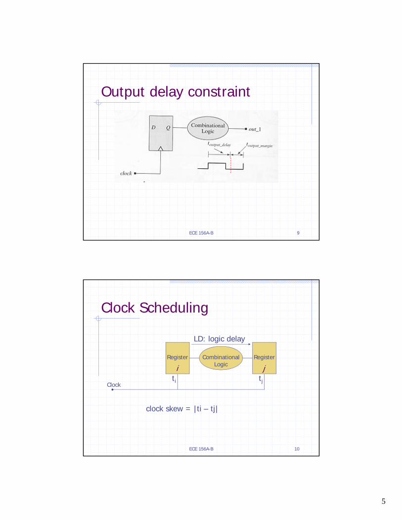
Clock Scheduling
Register Combinational Logic
Register
Clock
i jti tj
LD: logic delay
clock skew = |ti – tj|
6
ECE 156A-B 11
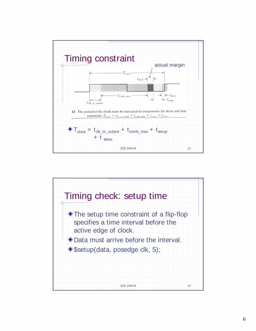
Timing constraint
Tclock > tclk_to_output + tcomb_max + tsetup
+ t skew
actual margin
ECE 156A-B 12
Timing check: setup time
The setup time constraint of a flip-flop specifies a time interval before the active edge of clock.Data must arrive before the interval.$setup(data, posedge clk, 5);

7
ECE 156A-B 13
Setup time example
ECE 156A-B 14
Timing check: hold time
The hold time constraint specifies an interval after the active edge of clock.Data must be stable in the interval.$hold(data, posedge clk, 2);

8
ECE 156A-B 15
Hold time example
ECE 156A-B 16
Pulse Width
The width of the clock pulse must not be too small.$width(posedge clock_a, t_mpw);
9
ECE 156A-B 17
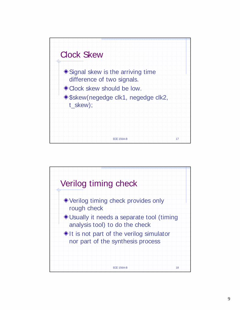
Clock Skew
Signal skew is the arriving time difference of two signals.Clock skew should be low.$skew(negedge clk1, negedge clk2, t_skew);
ECE 156A-B 18
Verilog timing check
Verilog timing check provides only rough check Usually it needs a separate tool (timing analysis tool) to do the checkIt is not part of the verilog simulator nor part of the synthesis process
10
ECE 156A-B 19
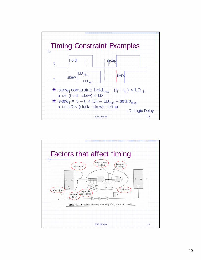
Timing Constraint Examples
skewij constraint: holdmax – (ti – tj ) < LDmini.e. (hold – skew) < LD
skewij = ti – tj < CP – LDmax – setupmaxi.e. LD < (clock – skew) – setup
tj
ti
hold setup
LDmin
LDmax
LD: Logic Delay
skewskew
ECE 156A-B 20
Factors that affect timing

11
ECE 156A-B 21
Multiple clock domains
clock skew = arrival time of clk_1 – arrive time of clk_2
ECE 156A-B 22
Model to check via timing DAG (find worst LDs between FFs)

12
ECE 156A-B 23
Static Timing Analysis
Arrival time: input -> output, (take max)Required arrival time: output -> input, (take min)Slack = required arrival time – arrival time
2
3
4
3
7
11
2
3
7/4/-3
5/3/-2
4/7/3
8/8/0
9/6/-3
20/17/-3
11/11/0
18/18/0
23/20/-3
given
ECE 156A-B 24
False Paths (don’t affect timing)
[3:5, 2:3] [3:5, 2:3] [3:5, 2:3]
Min, max rising Min, max falling
Max path delay = 15?
1
0
Can’t be sensitized!
1 0 1 0

13
ECE 156A-B 25
Logical false path
ECE 156A-B 26
Dynamically Sensitized Paths
a b
c
d
‘0’
a
b
c
d
The path is not logicallysensitizable but time-wiseit can be
14
ECE 156A-B 27
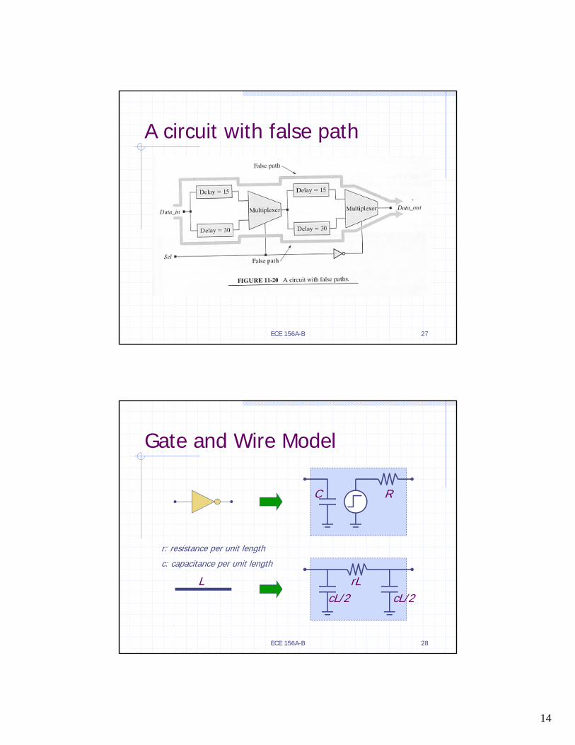
A circuit with false path
ECE 156A-B 28
Gate and Wire Model
C R
L rLcL/2 cL/2
r: resistance per unit length
c: capacitance per unit length

15
ECE 156A-B 29
Example of Model
0 1
2
3
L1
L2
L3
C2
C3
0 1
2
3
R rL1
rL2
rL3
cL1/2
(L1+L2+L3)c/2
cL2/2+C2
cL3/2+C3
ECE 156A-B 30
Delay Estimation
D0 = R ( C0 + C1 + C2 + C3 )D1 = D0 + R1 ( C1 + C2 + C3 )D2 = D1 + R2 C2
D3 = D1 + R3 C3
0 1
2
3
R R1
R2
R3
C0
C2
C3
C1

16
ECE 156A-B 31
Interconnect Delay
Interconnect delay is caused by parasitic capacitance and resistance
C C
R
ECE 156A-B 32
Myth:Interconnect Dominates?
05
1015202530354045
850 500 350 250 180 130 100
Gate
Interconnect(Al+SiO2)Interconnect(Cu+lowk)Sum (Al+SiO2)
Sum(Cu+lowk)
Generation (nm)
Delay(ps)
17
ECE 156A-B 33
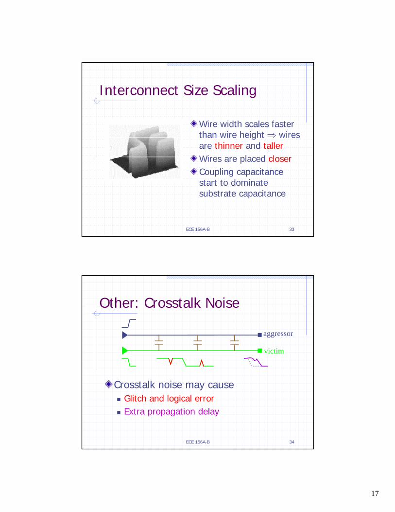
Interconnect Size Scaling
Wire width scales faster than wire height ⇒ wires are thinner and tallerWires are placed closerCoupling capacitance start to dominate substrate capacitance
ECE 156A-B 34
Other: Crosstalk Noise
Crosstalk noise may causeGlitch and logical errorExtra propagation delay
aggressor
victim
18
ECE 156A-B 35
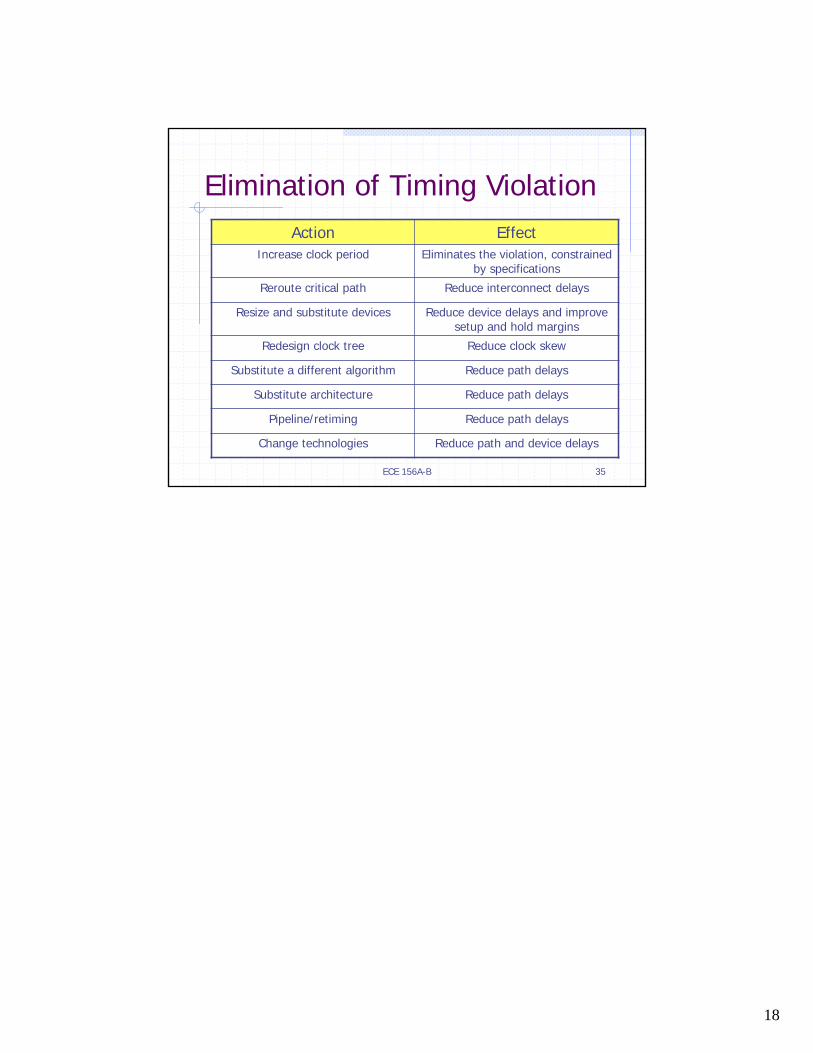
Elimination of Timing Violation Action Effect
Increase clock period Eliminates the violation, constrained by specifications
Reroute critical path Reduce interconnect delays
Resize and substitute devices Reduce device delays and improve setup and hold margins
Redesign clock tree Reduce clock skew
Substitute a different algorithm Reduce path delays
Substitute architecture Reduce path delays
Pipeline/retiming Reduce path delays
Change technologies Reduce path and device delays