Timing
43
-
Upload
ammayi9845930467904 -
Category
Documents
-
view
1 -
download
0
description
good one
Transcript of Timing

TIMING ISSUES IN
MULTI-LEVEL LOGIC
OPTIMIZATION
c Giovanni De Micheli
Stanford University

Outline
c GDM
� Timing veri�cation.
{ Delay modeling.
{ Critical paths.
{ The false path problem.
� Algorithms for timing optimization.

Timing veri�cation and optimization
c GDM
� Veri�cation:
{ Check that a circuit runs at speed:
� Satis�es I/O delay constraints.
� Satis�es cycle-time constraints.
� Optimization:
{ Minimum area
� subject to delay constraints.
{ Minimum delay
� (subject to area constraints).
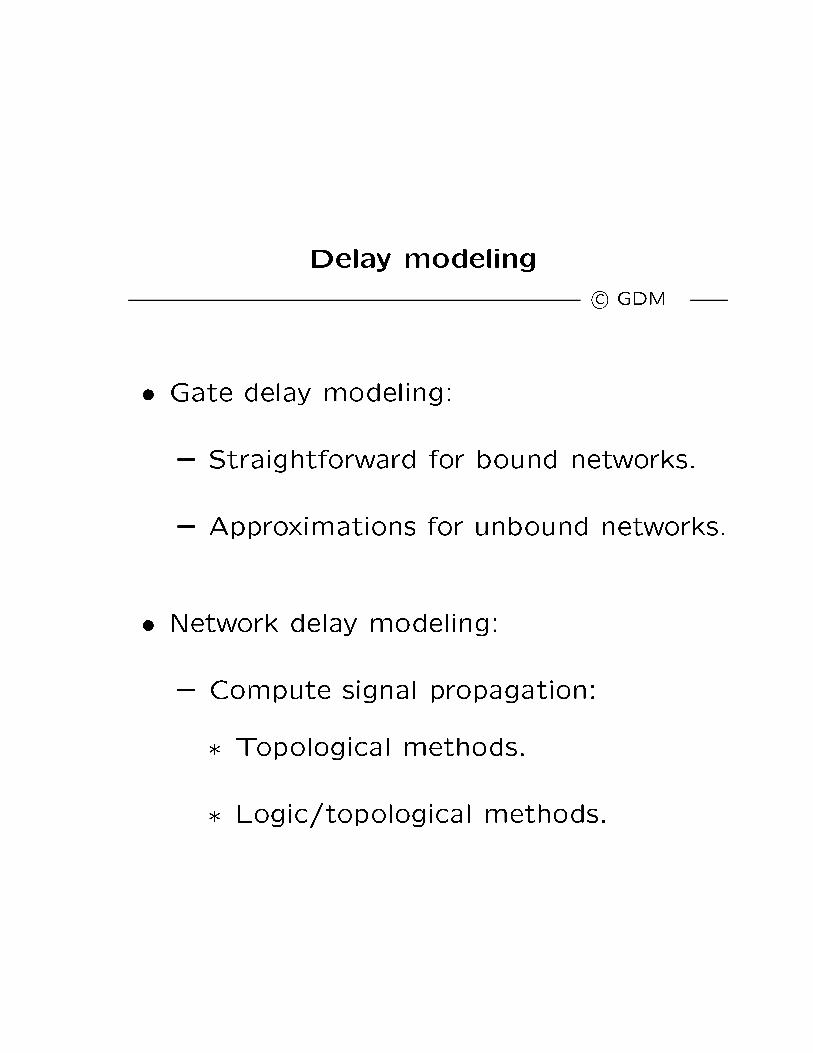
Delay modeling
c GDM
� Gate delay modeling:
{ Straightforward for bound networks.
{ Approximations for unbound networks.
� Network delay modeling:
{ Compute signal propagation:
� Topological methods.
� Logic/topological methods.
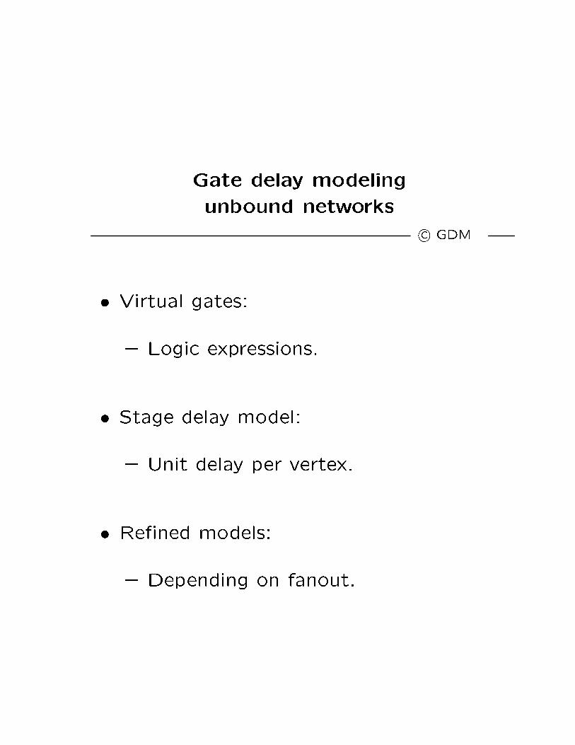
Gate delay modeling
unbound networks
c GDM
� Virtual gates:
{ Logic expressions.
� Stage delay model:
{ Unit delay per vertex.
� Re�ned models:
{ Depending on fanout.

Network delay modeling
c GDM
� For each vertex vi.
� Propagation delay di.
{ I/O propagation delays are usually zero.
� Data-ready time ti.
{ Input data-ready times denote when
inputs are available.
{ Computed elsewhere by forward traversal:
{ ti = di + maxjj(vj;vi)2E
tj

Example
c GDM
0 5 10 15 20 25
a
b
x
y
g
h
k l
m
n
p q
data−ready
� Propagation delays:
{ dg = 3; dh = 8; dm = 1; dk = 10; dl = 3;
{ dn = 5; dp = 2; dq = 2; dx = 2; dy = 3;

Network delay modeling
c GDM
� For each vertex vi.
� Required data-ready time tx.
{ Speci�ed at the primary outputs.
{ Computed elsewhere by backward traversal:
{ ti = minjj(vi;vj)2E
tj � dj
� Slack si.
{ Di�erence between required and
actual data-ready times si = ti � ti.

Example
c GDM
0 5 10 15 20 25
a
b
x
y
g
h
k l
m
n
p q
data−ready
� Required data-ready times:
{ tx = 25 and ty = 25.

Example
c GDM
� sx = 2; sy = 0
� tm = 25� 2 = 23; sm = 23� 21 = 2;
� tq = 25� 3 = 22; sq = 22� 22 = 0;
� tl = minf23� 1; 22� 2g = 20; sl = 20� 20 = 0;
� th = 23� 1 = 22; sh = 22� 11 = 11;
� tk = 20� 3 = 17; sk = 17� 13 = 4;
� tp = 20� 3 = 17; sp = 17� 17 = 0;
� tn = 17� 2 = 15; sn = 15� 15 = 0;
� tb = 15� 5 = 10; sb = 10� 10 = 0;
� tg = minf22� 11; 17� 10; 17� 2g = 7; sg = 7� 3 = 4;
� ta = 7� 3 = 4; sb = 4� 0 = 4.
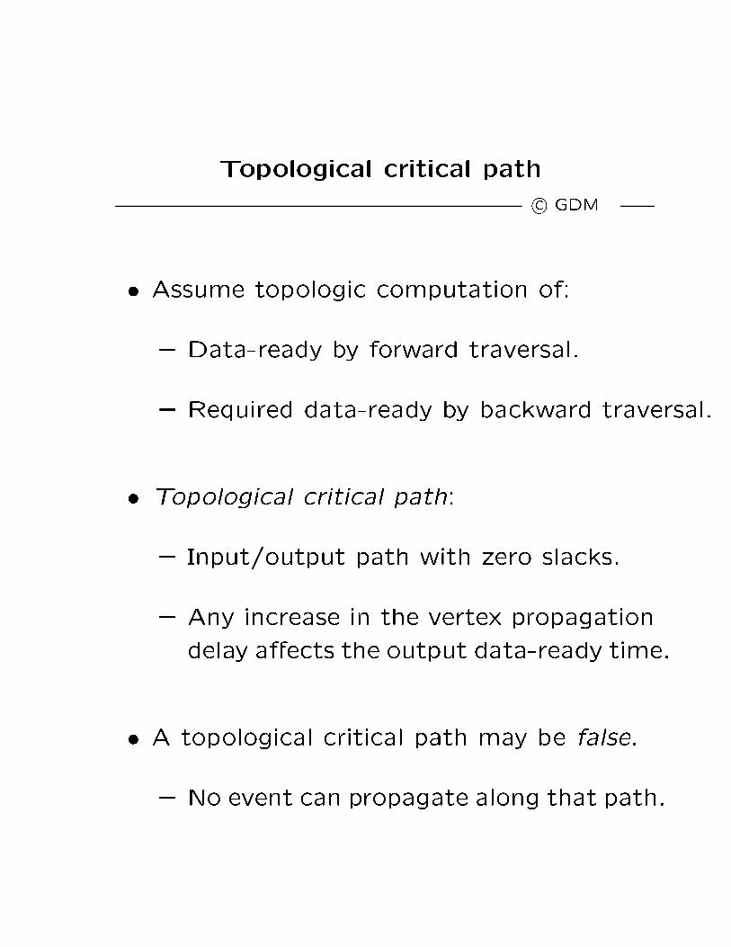
Topological critical path
c GDM
� Assume topologic computation of:
{ Data-ready by forward traversal.
{ Required data-ready by backward traversal.
� Topological critical path:
{ Input/output path with zero slacks.
{ Any increase in the vertex propagation
delay a�ects the output data-ready time.
� A topological critical path may be false.
{ No event can propagate along that path.

Example
c GDM
0 5 10 15 20 25
a
b
x
y
g
h
k l
m
n
p q
data−ready
s=0 s=0
s=0
s=0
s=0s=0
s=11 s=2 s=2
s=4s=4s=4

Example
c GDM
ya
b
c
z
d
e
� All gates have unit delay.
� All inputs ready at time 0.
� Longest topological path: (va; vc; vd; vy; vz).
{ Path delay: 4 units.
� Critical true path: (va; vc; vd; vy).
{ Path delay: 3 units.

Sensitizable paths
c GDM
� A path in a logic network is sensitizable if
an event can propagate from its tail to its
head.
� A critical path is a sensitizable path of
maximum weight.
� Only sensitizable paths should be
considered.
� Non-sensitizable paths are false
and can be discarded.

Sensitizable paths
c GDM
� Path:
{ Ordered set of vertices.
� Inputs to a vertex:
{ Direct predecessors.
� Side-inputs of a vertex:
{ Inputs not on the path.
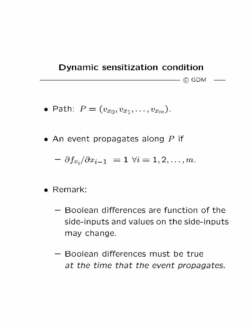
Dynamic sensitization condition
c GDM
� Path: P = (vx0; vx1; : : : ; vxm).
� An event propagates along P if
{ @fxi=@xi�1 = 1 8i= 1;2; : : : ;m.
� Remark:
{ Boolean di�erences are function of the
side-inputs and values on the side-inputs
may change.
{ Boolean di�erences must be true
at the time that the event propagates.

Example
c GDM
ya
b
c
z
d
e
� Path: (va; vc; vd; vy; vz)
{ @fy=@d= e = 1 at time 2.
{ @fz=@y = e0 = 1 at time 3.
� Not dynamically sensitizable
because e settles at time 1.

Static sensitization
c GDM
� Simpler, weaker model.
� We neglect the requirement on when the
Boolean di�erences must be true to
propagate an event.
� There is an assignment of primary inputs c
such that @fxi(c)=@xi�1 = 1 8i= 1;2; : : : ;m.
� May lead to underestimate delays.
Example
c GDM
ya
b
c
z
d
e
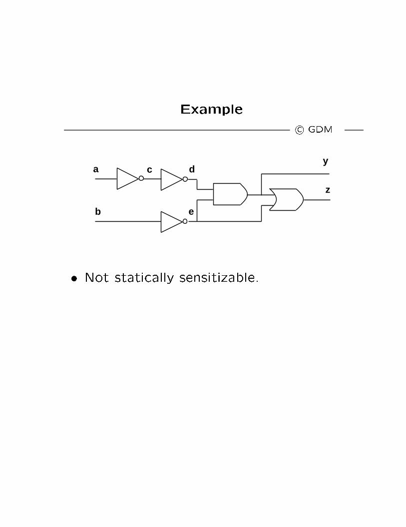
� Not statically sensitizable.

Example
c GDM
a
b
c
d
e
g
o
� All gates have unit propagation delay.

Example
c GDM
� Topological critical paths:
{ f(va; vd; vg; vo); (vb; vd; vg; vo)g
{ Path delay: 3.
{ Not statically sensitizable.
� Other path:
{ (va; ve; vo)
{ Path delay: 2.
� Assume:
{ c = 0 and a; b dropping from 1 to 0.
{ Event propagates to output !!!
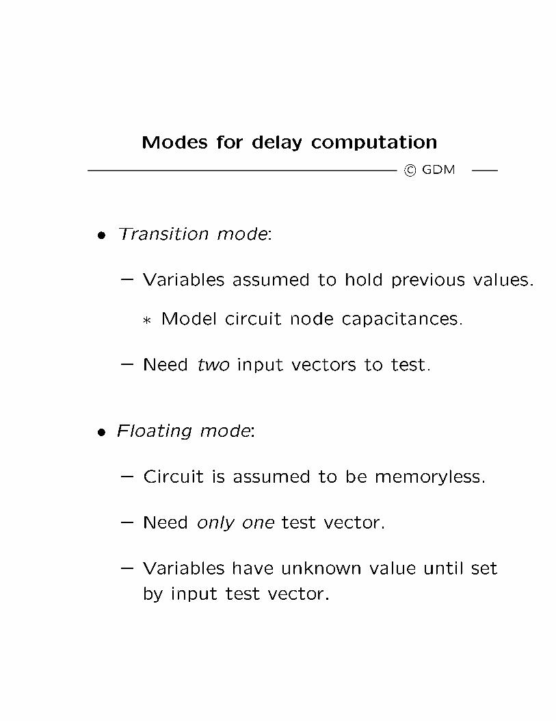
Modes for delay computation
c GDM
� Transition mode:
{ Variables assumed to hold previous values.
� Model circuit node capacitances.
{ Need two input vectors to test.
� Floating mode:
{ Circuit is assumed to be memoryless.
{ Need only one test vector.
{ Variables have unknown value until set
by input test vector.

Modes for delay computation
c GDM
� Floating mode delay computation is
simpler than transition mode computation.
� Floating mode is a pessimistic approach.
� Floating mode is more robust:
{ Transition mode may not have the
monotone speed-up property.

Monotone speed-up property
c GDM
� Propagation delays are upper bounds.
{ What happens if gates are faster
than expected?
� We must insure that speeding-up a gate
does not slow-down the circuit.
{ Topological critical paths are robust.
{ What about dynamically sensitizable paths
in transition mode?

Example
c GDM
y
a
x
u
v
o
w
a
u
x
v
y
o
w
0 1 2 3 4 5 6 7
time
a
u
x
v
y
o
w
0 1 2 3 4 5 6 7
time
(a)
(b) (c)
� Propagation delays: 2 units.
� Shaded gate: 3 units and 1 unit.

Static co-sensitization
c GDM
� Assumption:
{ Circuit modeled by AND;OR; INV gates.
{ INV are irrelevant to the analysis.
{ Floating mode.
� Controlling values:
{ 0 for AND gate.
{ 1 for OR gate.
� Gate has controlled value.

Static co-sensitization
c GDM
� Path: P = (vx0; vx1; : : : ; vxm).
� A vector statically co-sensitizes a path to 1
(or to 0) if
{ xm = 1 or (0) and
{ vxi�1 has a controlling value whenever
vxi has a controlled value.
� Necessary condition for a path to be true.

False path detection test
c GDM
� For all input vectors, one of the following is true:
{ (1) A gate is controlled and
� the path provides a non-controlling value
� a side-input provides a controlling value.
{ (2) A gate is controlled and
� the path and a side-input have controllingvalues
� the side-input presents the controlling value�rst.
{ (3) A gate is not controlled and
� a side-input presents the non-controlling value
last.

Example
c GDM
ya
b
c
z
d
e
� Path: (va; vc; vd; vy; vz).
� For a = 0; b = 0
{ condition (1) occurs at the OR gate.
� For a = 0; b = 1
{ condition (2) occurs at the AND gate.
� For a = 1; b = 0
{ condition (2) occurs at the OR gate.
� For a = 1; b = 1
{ condition (1) occurs at the AND gate.

Important problems
c GDM
� Check if circuit works at speed t.
{ Verify that all true paths are faster than t.
{ Show that all paths slower than t are
false.
� Compute groups of false paths.
� Compute critical true path:
{ Binary search for values of t.
{ Show that all paths slower than t are
false.

Algorithms for delay minimization
c GDM
� Alternate:
{ Critical path computation.
{ Logic transformation on critical vertices.
� Consider quasi critical paths:
{ Paths with near-critical delay.
{ Small slacks.

Algorithms for delay minimization
c GDM
REDUCE DELAY ( Gn(V;E) ; �)f
repeat f
Compute critical paths and critical delay � ;
Set output required data-ready times to � ;
Compute slacks;
U = vertex subset with slack lower than �;
W = select vertices in U ;
Apply transformations to vertices W ;
guntil (no transformation can reduce � );
g

Transformations for delay reduction
c GDM
� Reduce propagation delay.
� Reduce dependencies from critical inputs.
� Favorable transformation:
{ Reduces local data-ready time.
{ Any data-ready time increase at other
vertices is bounded by the local slack.

Example
c GDM
� Unit gate delay.
� Transformation:
{ Elimination.
� Always favorable.
� Obtain several area/delay trade-o� points.

Example
c GDM
a
b
c
d
e
g
hk
l
m
x
y
w
z
p
q
r
s
t
u
(a)
a
b
c
d
e
g
hk
l
m
x
y
w
z
r
s
t
(b)
� Iteration 1: eliminate vp; vq. (No literal increase.)
� Iteration 2: eliminate vu. (No literal increase.)
� Iteration 3: eliminate vr; vs; vt. (Literals increase.)

More re�ned delay models
c GDM
� Elimination:
{ Reduces one stage.
{ Yields more complex and slower gates.
{ May slow other paths.
� Substitution:
{ Adds one dependency.
{ Loads and slows a gate.
{ May slow other paths.

Example
c GDM
k j i
j
k i
x
y
z
c
a
b
e
d
x
y
z
c
a
b
e
d
(a) (b)
(c) (d)
m m
k k

Example
c GDM
y
abc x
de
g
y
abc
x
de
g
a’+b’+c’+d’+e’
y
a
bc x
d
e
g
e
d
� NAND delay =2. INVERTER delay =1.
� All input data-ready are 0, except td = 3.
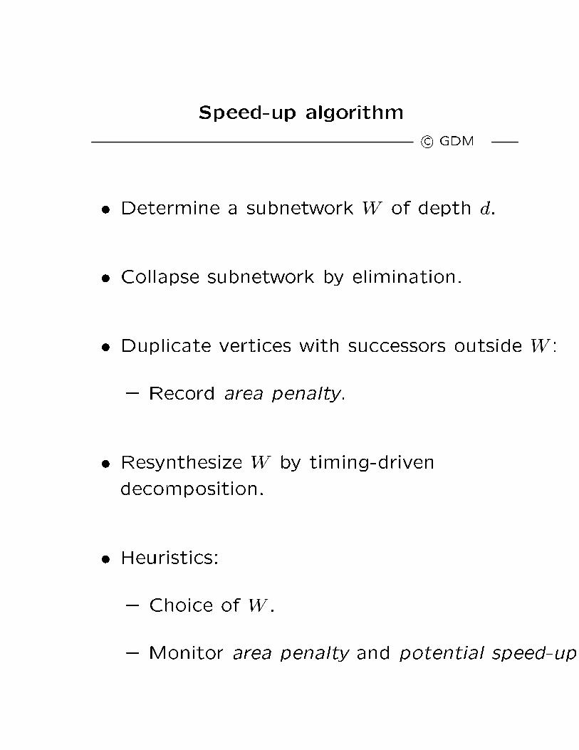
Speed-up algorithm
c GDM
� Determine a subnetwork W of depth d.
� Collapse subnetwork by elimination.
� Duplicate vertices with successors outside W :
{ Record area penalty.
� Resynthesize W by timing-driven
decomposition.
� Heuristics:
{ Choice of W .
{ Monitor area penalty and potential speed-up.
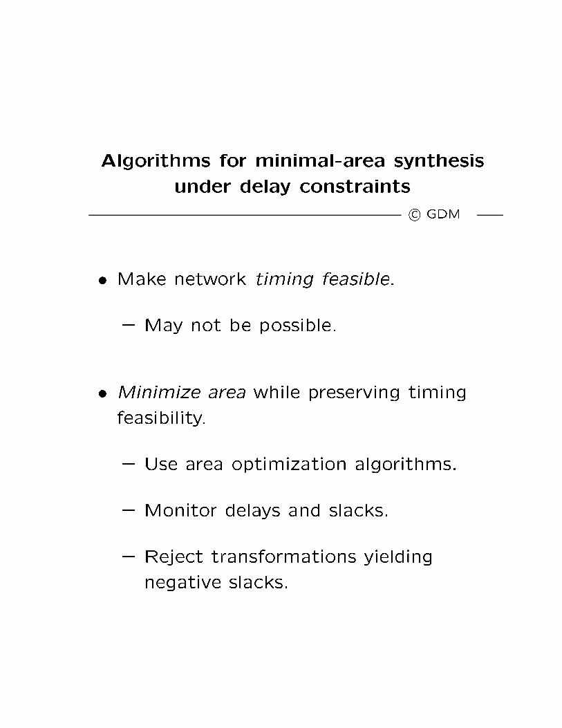
Algorithms for minimal-area synthesis
under delay constraints
c GDM
� Make network timing feasible.
{ May not be possible.
� Minimize area while preserving timing
feasibility.
{ Use area optimization algorithms.
{ Monitor delays and slacks.
{ Reject transformations yielding
negative slacks.

Making a network timing feasible.
c GDM
� Naive approach:
{ Mark vertices with negative slacks.
{ Apply transformations to marked vertices.
� Re�ned approach.
{ Transform multiple I/O delay constraints
into single constraint by delay padding.
{ Apply algorithms for CP minimization.
{ Stop when constraints are satis�ed.

Example
t = [2332]T
c GDM
a
b
c
d
e
g
hk
l
m
x
y
w
z
p
q
r
s
t
(a)
a
b
c
d
e
g
hk
l
m
x
y
w
z
r
s
t
(b)
u
u

Summary
c GDM
� Timing optimization is crucial for
achieving competitive logic design.
� Timing optimization problems are hard:
{ Detection of critical paths.
� Elimination of false paths.
{ Network transformations.