22 October 20151/23Fabio Vinagre -- TileCal DCS TileCal DCS Expert tutorial - DCS 22 October 2015.
Upload
jakobe-lyddonCategory
view
223download
1
TileCal Optical Multiplexer Board 9U VME Prototype
Cristobal Cuenca AlmenarIFIC (Universitat de Valencia-CSIC)

Outline
• Introduction• Previous work OMB 6U• Final prototype OMB 9U• Schedule for production

ATLAS detector

Optical Multiplexer Board
• 64 modules x 4 Barrels
• 2 links out per module with redundant data.
• Global CRC and DMU CRC.
8 OMBs x 4 cratesOMB: 16 In / 8 OutCRC checkingVME error countersData injection to RODs
8 RODs x 4 cratesROD: 8 In/ 2 outData processing
Outline
• Introduction• Previous work OMB 6U• Final prototype OMB 9U• Schedule for production
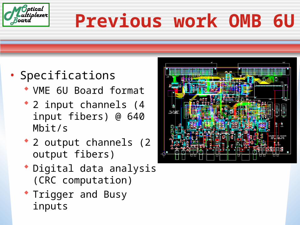
Previous work OMB 6U
• Specifications VME 6U Board format 2 input channels (4 input fibers) @ 640 Mbit/s
2 output channels (2 output fibers)
Digital data analysis (CRC computation)
Trigger and Busy inputs

VME_FPGA
•ALTERA ACEX FPGA EP1K100•VME R/W registers
•Status/control•CRC error registers
•Provides communication between VME bus and CRC_FPGAs.
2 CRC_FPGAs• Altera Cyclone® FPGA• Real-time CRC check• Internal memory lets us download and inject real events towards the ROD.• Event counter generator• CRC injection
OPTICAL I/O• 4 Optical transceivers I/O (Infineon®V23818-K305-L17)• 2 Inputs / 1 Output per each CRC_FPGA
SERIALIZERS/ DESERIALIZERS
• 4 receivers (HDMP 1034)•2 transmitters (HDMP1032)•The same ones as the I.C.s
VME INTERFACE
FP connectors• LEMO input conectors:
•Trigger and busy
Previous work OMB 6U

ROD production with the OMB 6U
• Front-End emulation with the OMB 6U.• Events injected with CRC• Online CRC checking
Total events injected: 13 x 109 events Total events checked: 1,7 x 10⁹ events

Outline
• Introduction• Previous work OMB 6U• Final prototype OMB 9U• Schedule for production

Final prototype OMB 9U
• Same basic functionality CRC checking Data injection 40 MHz clock
• Differences 8 channels
16 input fibers 8 output fibers
TTCrx Mezzanine connectors: more processing power?

PCB technical
specifications• PCB details
Input/output signals designed for operation at 80 MHz
• Standard 9U VME board size
• 1272 components• 2278 nets
10 copper layers Signal layers between power/gnd planes
Adjacent layers routed orthogonally for minimum coupling

OMB main components
CRCFPGA
CRCFPGA
CRCFPGA
CRCFPGA
CRCFPGA
CRCFPGA
CRCFPGA
CRCFPGA
DUAL RECEIVER
DUAL RECEIVER
DUAL RECEIVER
DUAL RECEIVER
DUAL RECEIVER
DUAL RECEIVER
DUAL RECEIVER
DUAL RECEIVER
DUAL
TRANSMITTER
DUAL
TRANSMITTER
DUAL
TRANSMITTER
DUAL TRANSMITTER
Processing Unit
ProcessingUnit
ProcessingUnit
ProcessingUnit
VMEFPGA
TTCFPGA
TTC rx
P1
P2
P3
G-Links
OPTICAL CONNECTORs (Stratos Lightwave) G_LINKS chips
(Agilent HDMP1032/34)8 CRC FPGAs
(Altera CYCLONE 324pins)4 Processing Units slotsVME FPGA
(Altera CYCLONE 400pins)TTC FPGA & TTCrx
(ALTERA ACEX 144pins)

OMB CRC checking
• 16 Front End inputs.
• 8 output to ROD
• Real time CRC checking.
GLOBAL DMU CRC
• TTC Information
BCID DMU check
• Error counters readable from VME.

OMB: ROD injector
• Data injector to RODs. Actual data Autogenerated data.
• Trigger: External source.
TTC information

OMB:Processing Units
Upgrade
• 4 Processing Units.
• Compatible with ROD PUs.
• Pre-processing of front end data.

Outline
• Introduction• Previous work OMB 6U• Final prototype OMB 9U• Schedule for production

Schedule
• First prototype validated.• Currently producing the second prototype with minor changes• Software and firmware adaptation from 6U board.• Production of 38 boards during the summer.• Installation in the ATLAS cavern at the end of the year.

Backup slides

Final prototype OMB 9U
P2 (160pin)
P1 (160pin)
O / E
O / E
O / E
O / E
E / O
E / O
O / E
O / E
O / E
O / E
E / O
E / O
O / E
O / E
O / E
O / E
E / O
E / O
O / E
O / E
O / E
O / E
E / O
E / O
VM E
CONT ROLF PGA
VoltageDC/DC
converter
P0
Drawer_1
Drawer_1'
ROD Co n tro ller VM E
acces fu n ctio n s:- CSR read/write- Reset board (e.g. in
case of sychronizationerrors)
- Configure for “16 to 8”or “16 to 4”
G-LINK TX
HDM P1032/
1022
G-LINK RX
HDM P1034
CRCF PGA
G-LINK RX
HDM P1034
G-LINK RX
HDM P1034
G-LINK RX
HDM P1034
G-LINK TX
HDM P1032/
1022
2 diff
2 diff
2 diff
2 diff
16@40M Hz
16@40M Hz
16@40M Hz
16@40M Hz
16@40M Hz
16@40M Hz
2 diff
2 diff
PECL LVTTL
CRCF PGA
G-LINK TX
HDM P1032/
1022
G-LINK RX
HDM P1034
CRC
F PGA
G-LINK RX
HDM P1034
G-LINK RX
HDM P1034
G-LINK RX
HDM P1034
G-LINK TX
HDM P1032/1022
2 diff
2 diff
2 diff
2 diff
16@40M Hz
16@40M Hz
16@40M Hz
16@40M Hz
16@40M Hz
16@40M Hz
2 diff
2 diff
PECL LVTTL
CRCF PGA
Drawer_2
Drawer_2'
Drawer_2
Drawer_2'
G-LINK TX
HDM P1032/
1022
G-LINK RX
HDM P1034
CRC
F PGA
G-LINK RX
HDM P1034
G-LINK RX
HDM P1034
G-LINK RX
HDM P1034
G-LINK TX
HDM P1032/1022
2 diff
2 diff
2 diff
2 diff
16@40M Hz
16@40M Hz
16@40M Hz
16@40M Hz
16@40M Hz
16@40M Hz
2 diff
2 diff
PECL LVTTL
CRCF PGADrawer_2
Drawer_2'
Drawer_2
Drawer_2'
RODx_1
RODx_2
G-LINK TX
HDM P1032/
1022
G-LINK RX
HDM P1034
CRCF PGA
G-LINK RX
HDM P1034
G-LINK RX
HDM P1034
G-LINK RX
HDM P1034
G-LINK TX
HDM P1032/
1022
2 diff
2 diff
2 diff
2 diff
16@40M Hz
16@40M Hz
16@40M Hz
16@40M Hz
16@40M Hz
16@40M Hz
2 diff
2 diff
PECL LVTTL
CRCF PGA
Drawer_1
Drawer_1'
RODx_1
RODx_2
Drawer_1
Drawer_1'
RODx_1
RODx_2
Drawer_1
Drawer_1'
RODx_1
RODx_2
2
P
U
CO
N
PU
CO
N
P
U
C
ON
P
U
C
ON
4@40MHZ
Clock circuit
40M Hzcrystal
o scillato r
Z ero d elayClo ck
Bu ffer
40M Hz
T T Crx
P3 (160pin)

Final prototype OMB 9U
• Signal integrity issues Big area, not too much populated
Long distance traces (high coupling) Clock distribution JTAG chain distribution VME-CRC FPGA serial bus
Different voltage supplies +3.3 Volt for FPGA I/O and some logic +1.5 Volt for FPGA cores (island) +5 Volt for logic +12 Volt for NIM/TTL conversion (ext. trigger input)

Final prototype OMB 9U
• Example of SI analysis: VME to CRC serial BUS Connected between the VME FPGA and all CRC FPGAs
For control, communication, configuration, etc.
4 lines: CLK, DATA0, DATA1, DATA2, DATA3
Frequency of operation 40 MHz

Final prototype OMB 9U
• First attempt Manual placement and routing of bus lines
Keep stubs short Keep same routing layer as much as possible
R, RC termination
• Problem Characteristic impedance change at T junction
Reflections at first FPGA creates InterSymbol Interference (ISI)
CRCFPGA VME
CONTROLFPGA
CRCFPGA
CRCFPGA
CRCFPGA
Termination
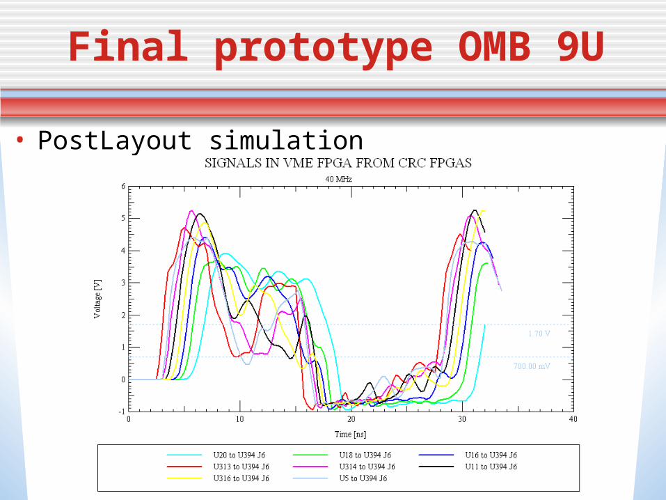
Final prototype OMB 9U
• PostLayout simulation

Final prototype OMB 9U
• Second attempt Manual placement and routing of bus lines
Keep stubs short Keep same routing layer as much as possible
• Problem Reflections with different termination schemes
CRCFPGA
VMECONTROL
FPGA
CRCFPGA
CRCFPGA
CRCFPGA
Termination
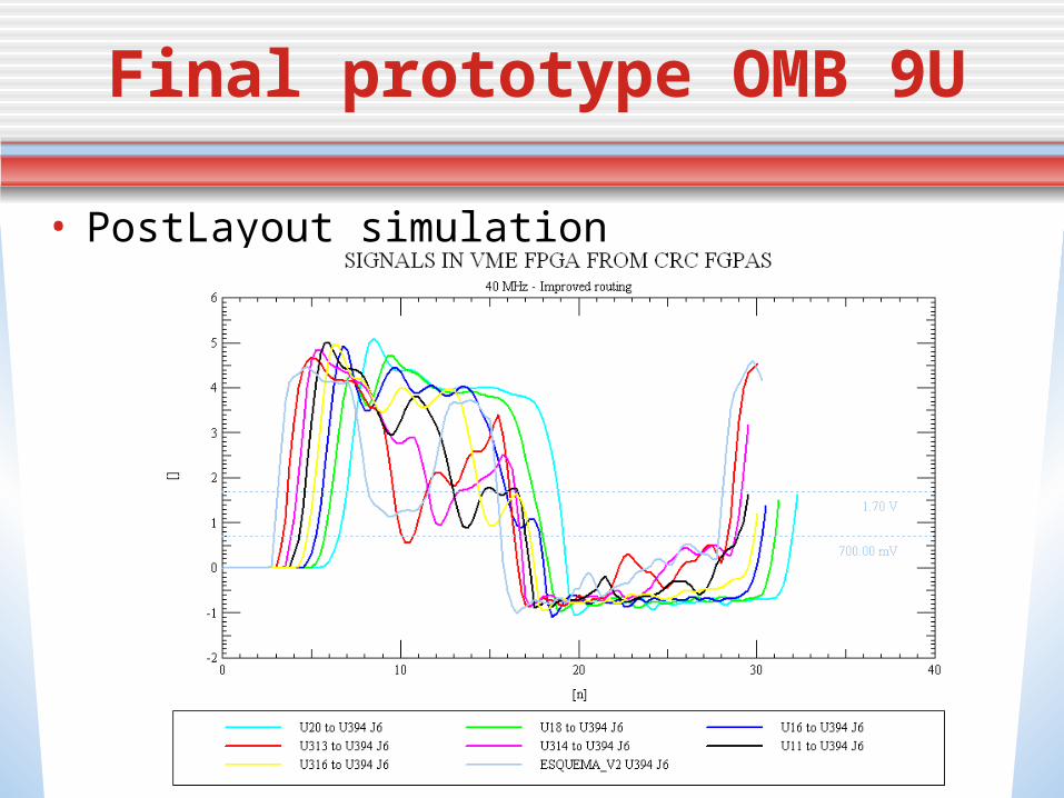
Final prototype OMB 9U
• PostLayout simulation

Final prototype OMB 9U
• Final attempt Manual placement and routing of bus lines
Keep stubs short Keep same routing layer as much as possible
• Solution Resistive termination at both ends
CRCFPGA
VMECONTROL
FPGA
CRCFPGA
CRCFPGA
CRCFPGA
Termination
Termination

Final prototype OMB 9U
• PostLayout simulation