Tic-tac-toe game design based on Xilinx FPGA - DiVA portal357030/FULLTEXT01.pdf · Technical...
65
Technical report, June 2010 Tic-tac-toe game design based on Xilinx FPGA Bachelor’s Thesis in Computer Science and Engineering Chi Zhang School of Information Science, Computer and Electrical Engineering, Halmstad University
Transcript of Tic-tac-toe game design based on Xilinx FPGA - DiVA portal357030/FULLTEXT01.pdf · Technical...
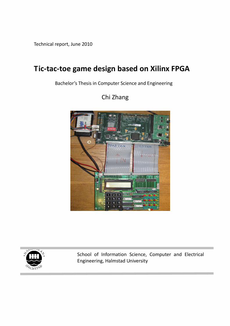
Technical report, June 2010
Tic-tac-toe game design based on Xilinx FPGA
Bachelor’s Thesis in Computer Science and Engineering
Chi Zhang
School of Information Science, Computer and Electrical
Engineering, Halmstad University

I
ACKNOWLEDGEMENT Academic Supervisor: Borje Dellstrand
Thanks for all the patient indoctrination from Borje during the three months’
hard work. Without your kind help, I couldn’t image a new learner in VHDL like
me could finish such a project on time. Thank you so much!
Also thanks Ruben Rydberg for the unselfish help when I met problems in
hardware part.
To my mother Caixia, Xu. For all the spiritual support and inspiritment.
II
ABSTRACT
This design accomplished Tic-Tac-Toe game on Xilinx Spartan-IIE FPGA platform
in VHDL. Firstly, designing the circuits and wiring on experiment board. Secondly,
designing the algorithm and programming it in Active-HDL. Thirdly, synthesizing
it in Synplicity Synplify Pro and then implementing it in Xilinx ISE developing
suite. Finally download it onto FPGA to run it.
This design allows two players to play Tic-Tac-Toe game on the experiment board.
Pressing the key, the corresponding LED will be light up to represent the
chessman. There are two LEDs indicate whose turn next is. If the grid one wants
to place chessman has been taken up, then LCD will alarm it and ask the player
to replace it. The first player who forms 3 chessmen in a row, column or diagonal
wins, LCD will display it and the three LEDs in the winning line will blink. If no
body wins after filling the whole chessboard, then LCD displays draw.
III
CONTENT ACKNOWLEDGEMENT ...................................................................................................................... I
ABSTRACT ....................................................................................................................................... II
CONTENT ....................................................................................................................................... III
1. INTRODUCTION ........................................................................................................................... 1
1.1. Background ........................................................................................................................... 1
1.2. Objective .............................................................................................................................. 1
2. METHOD ..................................................................................................................................... 3
2.1. FPGA Platform ....................................................................................................................... 3
2.2. Experiment board .................................................................................................................. 3
2.3. Components.......................................................................................................................... 3
2.3.1. LED array ........................................................................................................................ 3
2.3.2. Keyboard ........................................................................................................................ 4
2.3.3. Character Mode LCD ....................................................................................................... 4
2.4. Software developing environment .......................................................................................... 4
2.4.1. Active HDL ...................................................................................................................... 4
2.4.2. Synplicity Synplify Pro ..................................................................................................... 4
2.4.3. Xilinx ISE ......................................................................................................................... 5
2.5. ALGORITHM AND SOFTWARE MODULES ................................................................................. 6
2.5.1. Algorithm summary ........................................................................................................ 6
2.5.2. Finite State Machine ....................................................................................................... 7
2.5.3. Software modules ........................................................................................................... 8
3. CONCRETE DESIGN ...................................................................................................................... 9
3.1. Hardware design ................................................................................................................... 9
3.1.1. Expanding I/O ports ........................................................................................................ 9
3.1.2. LED array interface design ............................................................................................. 11
3.1.3. DTMF keypad ............................................................................................................... 14
3.1.4. Character LCD ............................................................................................................... 16
3.2. Software development ........................................................................................................ 20
3.2.1. Clock module ................................................................................................................ 20
3.2.2. Keypad driver ............................................................................................................... 20
3.2.3. Turn check .................................................................................................................... 22
IV
3.2.4. LED array driver ............................................................................................................ 23
3.2.5. Win check..................................................................................................................... 23
3.2.6. LED blink ...................................................................................................................... 23
3.2.7. LCD driver..................................................................................................................... 24
4. RESULT...................................................................................................................................... 25
4.1. Simulation result ................................................................................................................. 25
4.2. Synthesis result ................................................................................................................... 25
4.3. On board running result ....................................................................................................... 27
5. CONCLUSION............................................................................................................................. 28
REFERENCES ................................................................................................................................. 30
1
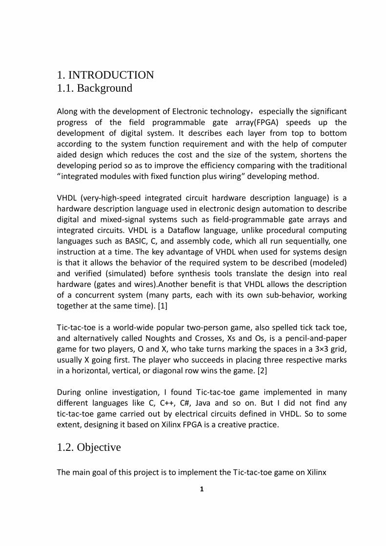
1. INTRODUCTION 1.1. Background
Along with the development of Electronic technology,especially the significant
progress of the field programmable gate array(FPGA) speeds up the
development of digital system. It describes each layer from top to bottom
according to the system function requirement and with the help of computer
aided design which reduces the cost and the size of the system, shortens the
developing period so as to improve the efficiency comparing with the traditional
“integrated modules with fixed function plus wiring” developing method.
VHDL (very-high-speed integrated circuit hardware description language) is a
hardware description language used in electronic design automation to describe
digital and mixed-signal systems such as field-programmable gate arrays and
integrated circuits. VHDL is a Dataflow language, unlike procedural computing
languages such as BASIC, C, and assembly code, which all run sequentially, one
instruction at a time. The key advantage of VHDL when used for systems design
is that it allows the behavior of the required system to be described (modeled)
and verified (simulated) before synthesis tools translate the design into real
hardware (gates and wires).Another benefit is that VHDL allows the description
of a concurrent system (many parts, each with its own sub-behavior, working
together at the same time). [1]
Tic-tac-toe is a world-wide popular two-person game, also spelled tick tack toe,
and alternatively called Noughts and Crosses, Xs and Os, is a pencil-and-paper
game for two players, O and X, who take turns marking the spaces in a 3×3 grid,
usually X going first. The player who succeeds in placing three respective marks
in a horizontal, vertical, or diagonal row wins the game. [2]
During online investigation, I found Tic-tac-toe game implemented in many
different languages like C, C++, C#, Java and so on. But I did not find any
tic-tac-toe game carried out by electrical circuits defined in VHDL. So to some
extent, designing it based on Xilinx FPGA is a creative practice.
1.2. Objective The main goal of this project is to implement the Tic-tac-toe game on Xilinx
2
FPGA so two persons could play on it. To accomplish this task, firstly, the
hardware part should be designed and the corresponding components to achive
it should be chosen. Secondly, I/O expanding circuits need to be built. Thirdly,
the algrithm of Tic-tac-toe need to be developed.Furthermore, the VHDL block
diagram should be programmed according to the algorithm.Finally, a testbench
should be programmed to emulate the program and then analyze the system in
the aspects of Timing and Area.
3
2. METHOD 2.1. FPGA Platform
The FPGA used in this design is Xilinx Spartan-IIE. The system board utilizes the
300,000 gate Xilinx Spartan-IIE device (XC2S300E5FG456C) in the 456 fine-pitch
ball grid array package. It has 6912 logic cells and 60 gerneral I/O which is
enough for this design.
Spartan-IIE is a low cost FPGA which has following features at low system cost:
� Embedded 18x18 multiplier which support high performance DSP
application.
� Digital clock management(DCM)
� Distributed storage and SRL16 shift register
� 18KB RAM
� 8 independent I/O array which support 24 different I/O standards.[3]
2.2. Experiment board
The experiment board used in the design was developed by Halmstad University,
the board connects the two I/O ports array JP6 and JP7 in FPGA with parallel
lines to the the experiment board, then connect to 74HC541D buffer, finally
connect to the I/O pins on board.
The board use wiring tool to wire on the pins, so welding is not needed which is
convinient to modify and easier for new-learner. The power module is also
embedded on the board which uses +5V. As the experiment board and FPGA are
connected by parallel lines, they do not share the same ground. FPGA recognises
signal according to the voltage, and the voltage is comparing to ground. So
different ground could lead to errors. In the design, a wire connects the ground
pin of both boards to solve the problem.
2.3. Components 2.3.1. LED array The design utilizes red and yellow LEDs to represent the two players. There are
20 LEDs in total, 18 of which forms the 3 x 3 chess board, it represents the place
4
has been taken by red side when red LED is on, so does yellow LED. The other
two LEDs indicate the turn of which side.
2.3.2. Keyboard This design employed a 4 x 3 keyboard as input. Num 1, 2, 3 in line 1 is
corresponding to the three group of LEDs in the first line of LED array
respectively. When one press one key, it will light up the corresponding LED, so
do line 2 and 3. The fourth is defined but doesn’t attach any action, which needs
future expansion.
2.3.3. Character Mode LCD This design used a 1602 Character Mode LCD as an indicator to improve
human-device interaction friendship. It’s an industrial character mode LCD which
could display two lines of 16 characters. It shows ”welcome” after powering on.
It displays ”the place has been taken” when a key is pressed more than once.
When one side wins, it displays ”win”, when draw, it displays ”draw”.
2.4. Software developing environment 2.4.1. Active HDL Active-HDL is an open simulating tool from ALDEC, it supports almost all
products from different FPGA/CPLD manufactories. The input could be principle
graph or hardware description language or FSM. The design could be more than
100 thousand gates. It supports VHDL, Verilog, SystemC and EDIF.[4]
Active-HDL supports the synthesizing and designing tools from different
FPGA/CPLD manufactories. The automatical flow manager accomplishes the
complete developing proceduces of input design, logical synthesis, layout and
the chip configuration. It’s the first complete solution of FPGA design and
validation.
2.4.2. Synplicity Synplify Pro
Synplify Pro is a logical synthesizing tool from Synplicity which focus on FPGA

5
and CPLD accomplishment. It performs optimization first at a high level before
synthesizing the RTL code into specific FPGA logic. This approach allows for
superior optimization across the FPGA, runs fast and supports very large design
sizes. The Synplify Pro software supports the latest VHDL and Verilog language
constructs including System Verilog and Verilog 2008. It supports
implementation in all leading FPGA devices from a variety of FPGA vendors,
including Actel, Altera, Lattice Semiconductor and Xilinx using a single
easy-to-use interface, with the ability to perform incremental synthesis and fast
incremental debugging. [5]
2.4.3. Xilinx ISE
Xilinx ISE is a software tool produced by Xilinx for synthesis and analysis of HDL
designs, which enables the developer to synthesize their designs, perform timing
analysis, examine RTL diagrams, simulate a design's reaction to different stimuli,
and configure the target device with the programmer.[6]
The project design procedures using ISE are as follow[7]:
1) Design Entry
The widely used input is HDL and principle graph. The graph is a basic input
method which user could use every kind of eletrical components in the
components library to form different scales of electrical circuits. But it is not easy
to maintain in large scale design, so HDL language is more popular nowadays,
among which VHDL and Verilog HDL are most widely used. Wave shape and FSM
input methods are the main aided design input method.
2) Synthesis
Synthesis translates action and function level electronical system to the
combination of low-level modules. In general, synthesis is for VHDL, i.e. it
translates models, algrithms and function description into netlists of
corresponding FPGA/CPLD basic structure.
Synthesis tools mainly include Synplify/Synplify Pro, FPGA Compiler II/ Express,
XST and etc., they optimise input and translate it into netlist which is consisted
by basic logical units such as AND, OR, NOT, RAM and Flip-Flop, then output edf
or edn files for further implementation.
6
3) Implementation
Implementation adapts netlists built by synthesis to fit different model of chips.
Implementation needs three procedures: Translate, Map,Place & Route. The
tools used in implementation are Constraints Editor, PACE, Timing Analyzer, FGPA
Editor, Chip Viewer and Floorplanner.
4) Verification
Verification contains two steps of simulation: Functional simulation and after
synthesis simulation. Functional simulation tests the logical function of designed
electronical circuit and see if it fulfill the requirements. Usually through viewing
waveform graph to find the relationship between input signal and output signal.
After synthesis simulation simulates the components close to their real
characteristics, it gives the accurate signal relay time between input and output.
5) Download
The last step is to download program onto developing board to process on chip
debug, the downloading tool in this design is iMPACT.
2.5. ALGORITHM AND SOFTWARE MODULES 2.5.1. Algorithm summary
To record the status of play, an array is needed to store every step. A 3 x 3 2D
array could store the whole chessboard. As the two sides need to be stored
separately, so two arrays X[r][c],Y[r][c] are employed. The initial value “0”
represents empty grid. After each step,set the corresponding element in the
arrays to “1” to represent the grid has been taken.
In order to input by keyboard, a module is needed to drive the key board. As the
steps of each side is stored separately, it could happen that one grid is taken
more than once. To avoid this abnormal situation, an availibility check is
necessary after each step, if the grid is “1”, then fail to pass the check, LCD
display alarm information and ask the player to choose another grid. If the grid is
“0”, it will pass the check and enter the next process.
The following task is to distiguish which side has made the current action. As
there will be two players who take turns to place chessman, so a one bit variable
7
t is employed to record turns, after each step, t+1, so it changes from “0” to “1”
and back to “0” after next step, and so forth. One thing should be caucious is
that one step may not pass the availibility check, so when it didn’t pass, t
shouldn’t plus one.
Then the coordinate of each step will be passed to LED driver and Win Check.
LED driver will light up the corresponding LED. Win Check process the winning
status. There are three kinds of win, line, column and diagonal, so three modules
are needed to check each situation. When doing line check, apply two loops to
visit every line, then do AND operation, unless the whole line are all “1”s, it will
not return “1” to indicate win. The column check is similar, just interchange the r
and c in loop condition. As for the three diagonals, it could simply check the
element [1][1],[2][2],[3][3]and[1][3],[2][2],[3][1]. Win check also need to check
the draw situation. In this design, the first placement is always stored in the first
array, so if draws, the first array will always has five “1”s. Then count the “1”s in
first array could tell if it is draw. But in this case, there is a problem that the first
player wins at the fifth step, then it will satisfy the conditions of both win and
draw. The solution is checking if it has already won, if not win, then check if it is
draw.
2.5.2. Finite State Machine
One of the features of VHDL programming is FSM, it refers to the timing logical
circuit whose output depends on both past input and current input. In general,
apart from input and output, FSM also has a set of registers. The function of
these registers is “remember” the internal status of FSM, they are usually called
status register.[8]
In practical application, depending on using input signal or not, FSM is usually
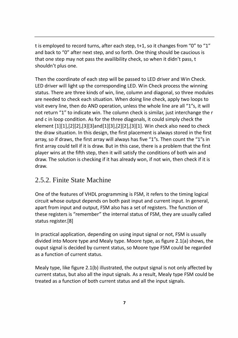
divided into Moore type and Mealy type. Moore type, as figure 2.1(a) shows, the
ouput signal is decided by current status, so Moore type FSM could be regarded
as a function of current status.
Mealy type, like figure 2.1(b) illustrated, the output signal is not only affected by
current status, but also all the input signals. As a result, Mealy type FSM could be
treated as a function of both current status and all the input signals.
8
Figure 2.1(a) Moore type FSM
Figure 2.1(b) Mealy type FSM
2.5.3. Software modules The software part consists the following modules:
1) Clock: the system need a clock to synchronize, the clock is from FPGA which
has a frequency of 24 MHZ, divide the clock and get a 100 HZ gobal clock clk100.
There is also a clock clkshake with duty ratio of 50% to control the twinkling of
LED.
2) Keyboard driver: It identifies if any key is pressed by producing line scan signal
and combining with column signal to get the pressed key. Every time a key is
pressed, it stores the “turn” value to the current array, then plus 1 to “turn”. If a
key has been pressed more than once, it will not change turn signal, instead, it
indicates the place has been taken.
3) Turn check: It records which player should make the next movement.
4) LED driver: It lights up the corresponding LED
9
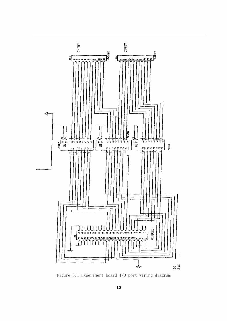
3. CONCRETE DESIGN 3.1. Hardware design 3.1.1. Expanding I/O ports Two parellel cables connect the general input ports and output ports on FGPA to
the input ports of 74HC541 buffer. Then from the output to the I/O ports of
experiment board. The wiring diagram is figure 3.1. As you can tell from the
diagram, to avoid confusion, the experiment board manually divides general I/O
ports into input ports and output ports, half of each. But in application, the
usage of output ports exceeds input ports. Meanwhile, the experiment board
does not use all of the general I/O ports, so in this design, the I/O ports are not
enough. To expand I/O ports, I welded the spare I/O ports on FPGA to
experiment board in the way exactly the same as other ports. Through this the
experiment board gained 16 more output ports. Then the current I/O ports on
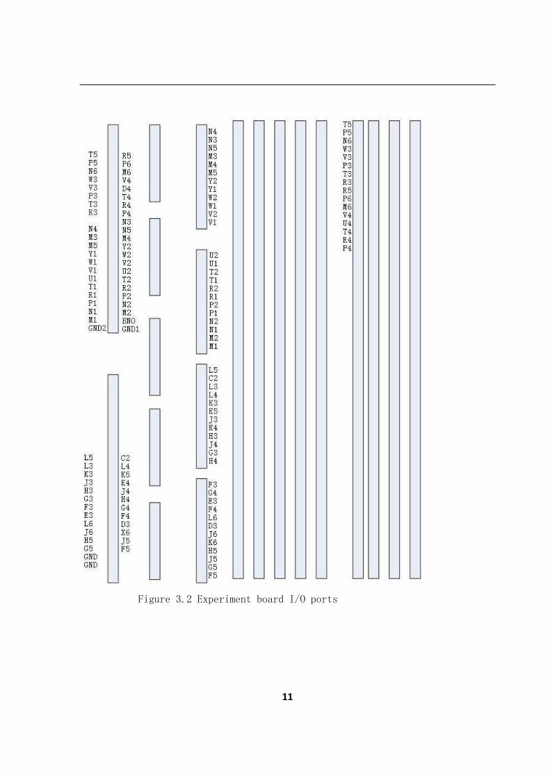
board is as shown in figure 3.2, within which the column T5 – P4 was expanded.
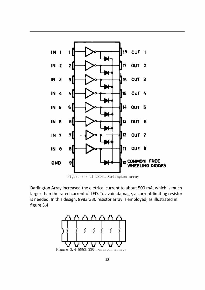
3.1.2. LED array interface design As LED is driven by electrical current, to get satisfied brightness, driven current
should be around 15 mA. But the I/O port in this FPGA could only supply a
current of 8 mA. To increase the current, an amplifying circuit is needed, in this
design, as many as 20 LEDs are used, so three uln2803a darlington arrays are
applied here. The principle of darlington array is shown in figure 3.3. Darlington
array is two audions connected to form a new equivalent audion with the
amplification factor of the product of both audions.
10
Figure 3.1 Experiment board I/O port wiring diagram
11
Figure 3.2 Experiment board I/O ports
12
Figure 3.3 uln2803a Darlington array
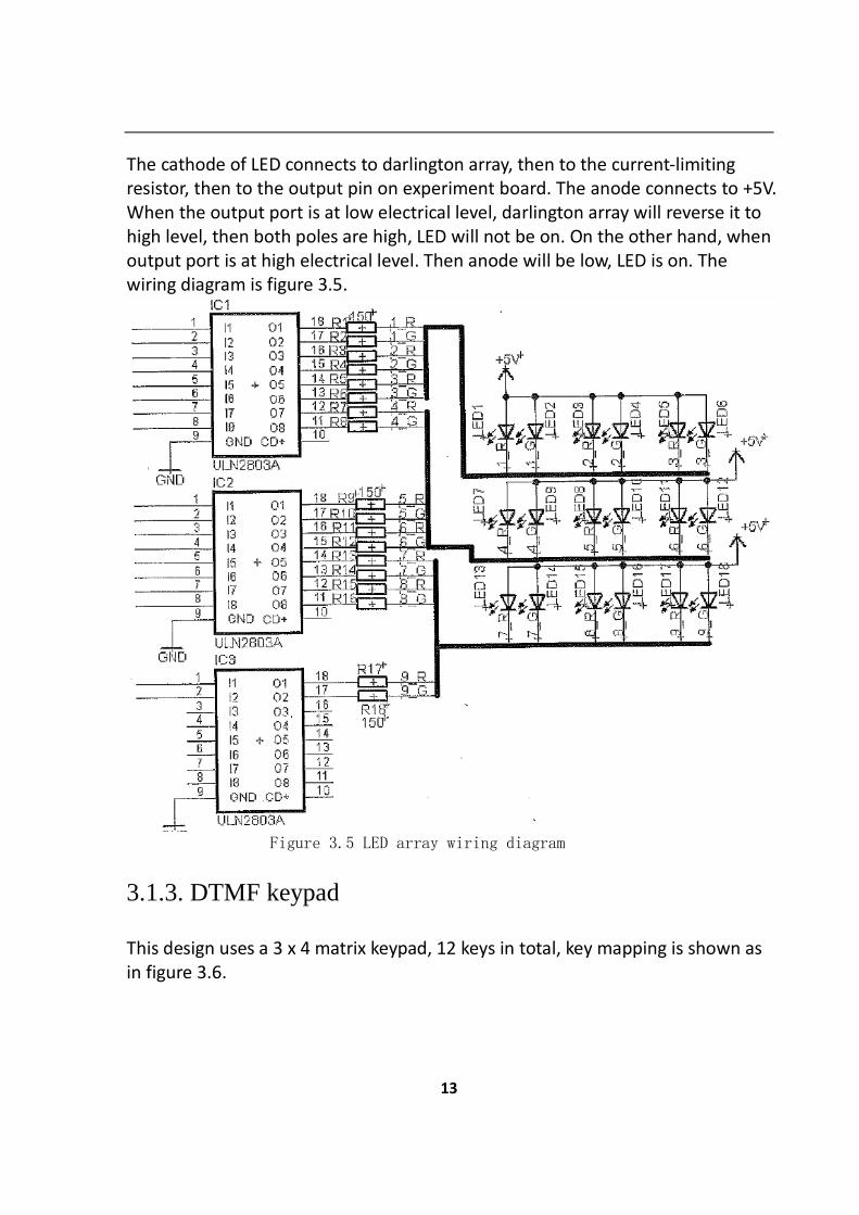
Darlington Array increased the eletrical current to about 500 mA, which is much
larger than the rated current of LED. To avoid damage, a current-limiting resistor
is needed. In this design, 8983r330 resistor array is employed, as illustrated in
figure 3.4.
Figure 3.4 8983r330 resistor arrays
13
The cathode of LED connects to darlington array, then to the current-limiting
resistor, then to the output pin on experiment board. The anode connects to +5V.
When the output port is at low electrical level, darlington array will reverse it to
high level, then both poles are high, LED will not be on. On the other hand, when
output port is at high electrical level. Then anode will be low, LED is on. The
wiring diagram is figure 3.5.
Figure 3.5 LED array wiring diagram
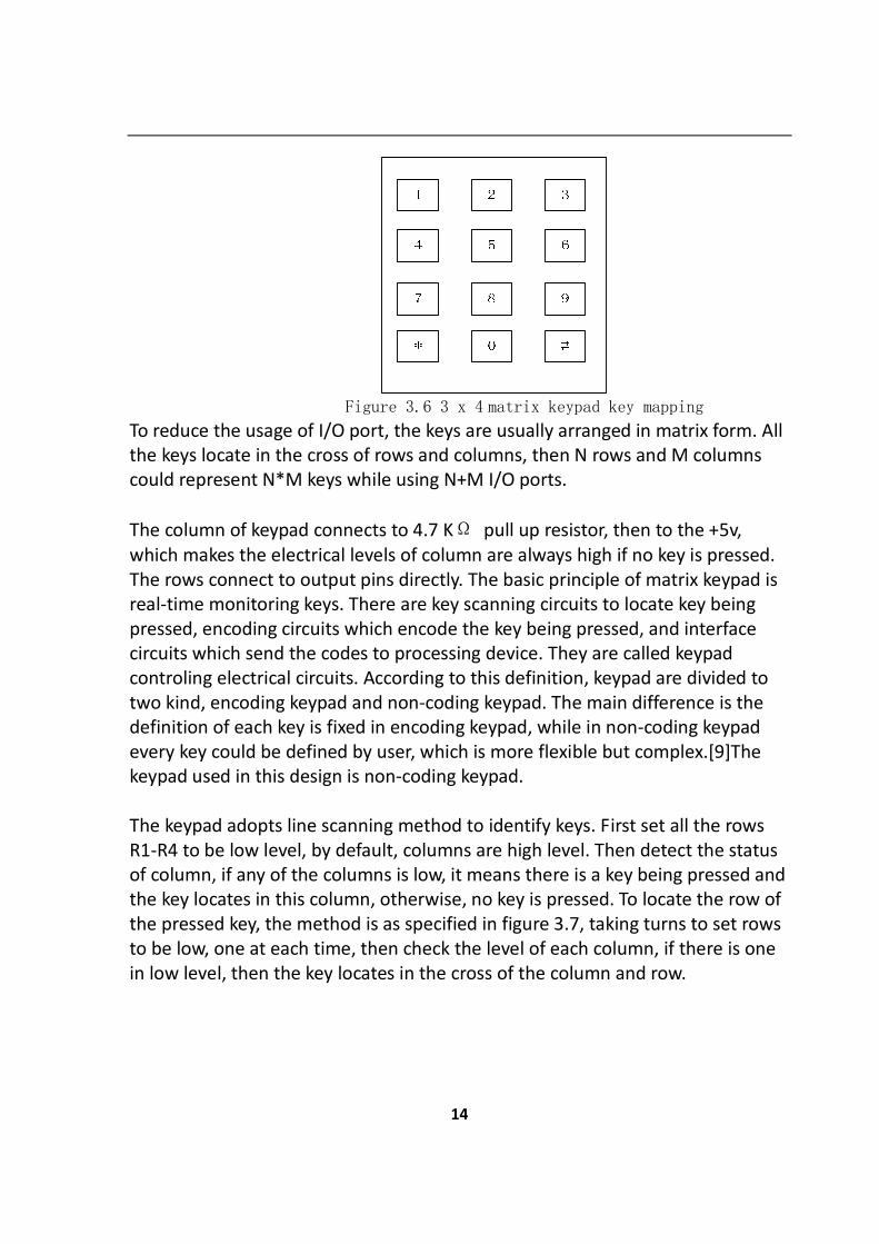
3.1.3. DTMF keypad This design uses a 3 x 4 matrix keypad, 12 keys in total, key mapping is shown as
in figure 3.6.
14
Figure 3.6 3 x 4 matrix keypad key mapping
To reduce the usage of I/O port, the keys are usually arranged in matrix form. All
the keys locate in the cross of rows and columns, then N rows and M columns
could represent N*M keys while using N+M I/O ports.
The column of keypad connects to 4.7 KΩ pull up resistor, then to the +5v,
which makes the electrical levels of column are always high if no key is pressed.
The rows connect to output pins directly. The basic principle of matrix keypad is
real-time monitoring keys. There are key scanning circuits to locate key being
pressed, encoding circuits which encode the key being pressed, and interface
circuits which send the codes to processing device. They are called keypad
controling electrical circuits. According to this definition, keypad are divided to
two kind, encoding keypad and non-coding keypad. The main difference is the
definition of each key is fixed in encoding keypad, while in non-coding keypad
every key could be defined by user, which is more flexible but complex.[9]The
keypad used in this design is non-coding keypad.
The keypad adopts line scanning method to identify keys. First set all the rows
R1-R4 to be low level, by default, columns are high level. Then detect the status
of column, if any of the columns is low, it means there is a key being pressed and
the key locates in this column, otherwise, no key is pressed. To locate the row of
the pressed key, the method is as specified in figure 3.7, taking turns to set rows
to be low, one at each time, then check the level of each column, if there is one
in low level, then the key locates in the cross of the column and row.
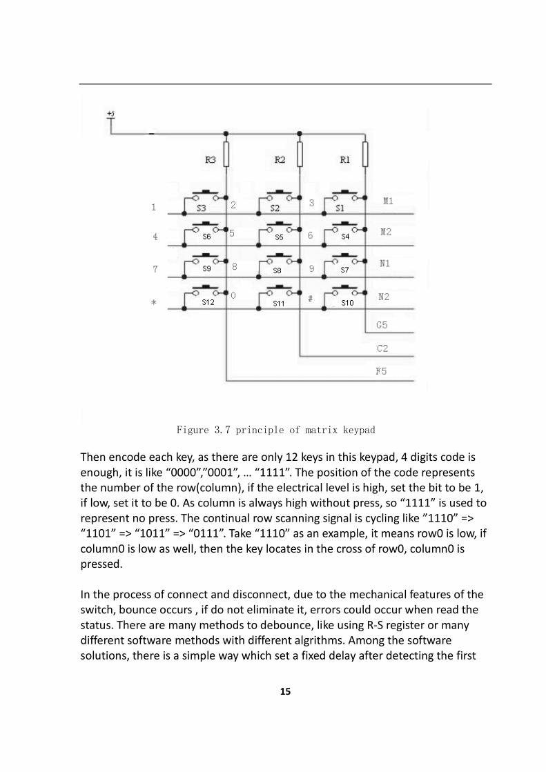
15
Figure 3.7 principle of matrix keypad
Then encode each key, as there are only 12 keys in this keypad, 4 digits code is
enough, it is like “0000”,”0001”, … “1111”. The position of the code represents
the number of the row(column), if the electrical level is high, set the bit to be 1,
if low, set it to be 0. As column is always high without press, so “1111” is used to
represent no press. The continual row scanning signal is cycling like ”1110” =>
“1101” => “1011” => “0111”. Take “1110” as an example, it means row0 is low, if
column0 is low as well, then the key locates in the cross of row0, column0 is
pressed.
In the process of connect and disconnect, due to the mechanical features of the
switch, bounce occurs , if do not eliminate it, errors could occur when read the
status. There are many methods to debounce, like using R-S register or many
different software methods with different algrithms. Among the software
solutions, there is a simple way which set a fixed delay after detecting the first
16
press to avoid regular shakes. This design uses this method.
In practice, column 1 was originally connected to port J5. Then a weird problem
occurred that the electrical circuit was alright and the simulation was also good,
but after downloading the program onto the FPGA, it didn’t work properly. The
electrical levels of all the pins from experiment board to FPGA were alright but
the FPGA simply did not recognize one of them. Another FPGA was tried but the
same problem remained. Then the connected I/O ports were changed and then
turned out to be another column did not work properly. Then the incorrect port
was tried on different ports and always not working until it was connected to G5.
Then some tests were carried out and proven that there were many mismatches
in the pin description file. It is very puzzling as the input ports are not so esiliy
tested as output ports do.
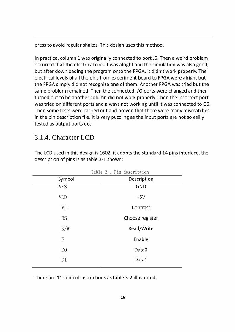
3.1.4. Character LCD The LCD used in this design is 1602, it adopts the standard 14 pins interface, the
description of pins is as table 3-1 shown:
Table 3.1 Pin description
Symbol Description
VSS GND
VDD +5V
VL Contrast
RS Choose register
R/W Read/Write
E Enable
D0 Data0
D1 Data1
There are 11 control instructions as table 3-2 illustrated:
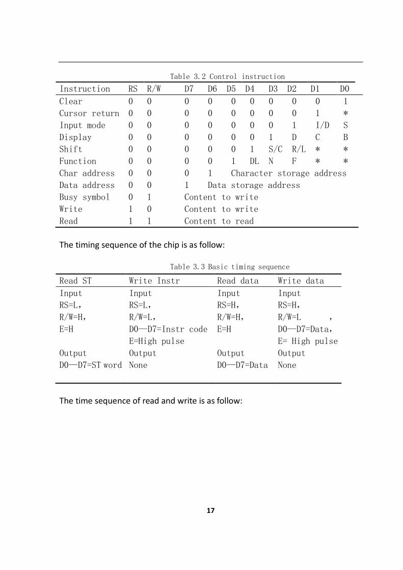
17
Table 3.2 Control instruction
Instruction RS R/W D7 D6 D5 D4 D3 D2 D1 D0
Clear 0 0 0 0 0 0 0 0 0 1
Cursor return 0 0 0 0 0 0 0 0 1 *
Input mode 0 0 0 0 0 0 0 1 I/D S
Display 0 0 0 0 0 0 1 D C B
Shift 0 0 0 0 0 1 S/C R/L * *
Function 0 0 0 0 1 DL N F * *
Char address 0 0 0 1 Character storage address
Data address 0 0 1 Data storage address
Busy symbol 0 1 Content to write
Write 1 0 Content to write
Read 1 1 Content to read
The timing sequence of the chip is as follow:
Table 3.3 Basic timing sequence
Read ST Write Instr Read data Write data
Input Input Input Input
RS=L,
R/W=H,
E=H
RS=L,
R/W=L,
D0—D7=Instr code
E=High pulse
RS=H,
R/W=H,
E=H
RS=H,
R/W=L ,
D0—D7=Data,
E= High pulse
Output Output Output Output
D0—D7=ST word None D0—D7=Data None
The time sequence of read and write is as follow:
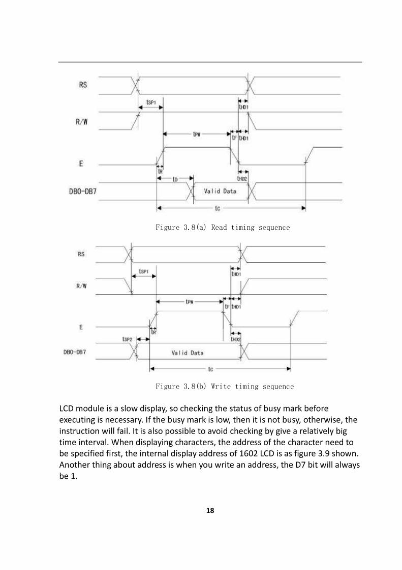
18
Figure 3.8(a) Read timing sequence
Figure 3.8(b) Write timing sequence
LCD module is a slow display, so checking the status of busy mark before
executing is necessary. If the busy mark is low, then it is not busy, otherwise, the
instruction will fail. It is also possible to avoid checking by give a relatively big
time interval. When displaying characters, the address of the character need to
be specified first, the internal display address of 1602 LCD is as figure 3.9 shown.
Another thing about address is when you write an address, the D7 bit will always
be 1.
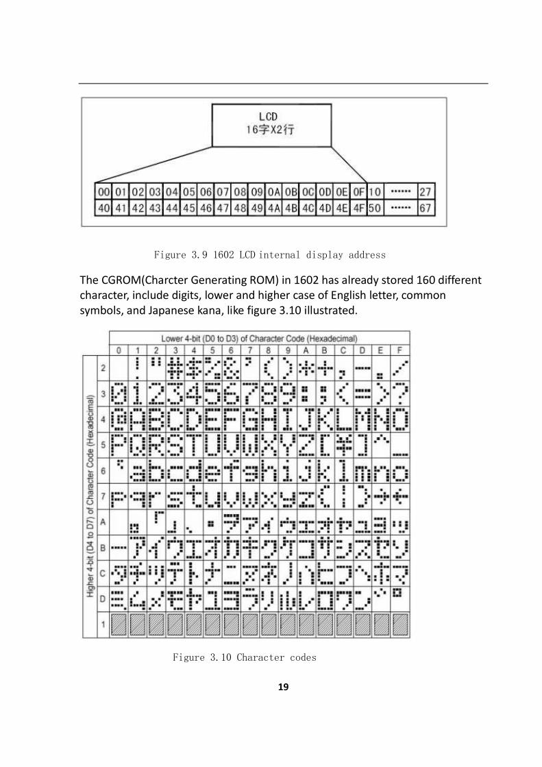
19
Figure 3.9 1602 LCD internal display address
The CGROM(Charcter Generating ROM) in 1602 has already stored 160 different
character, include digits, lower and higher case of English letter, common
symbols, and Japanese kana, like figure 3.10 illustrated.
Figure 3.10 Character codes
20
There are two reset processes before usage, one is hardware reset, once
electrified, the hardware reset will automaticly accomplished by hardware
circuits. The detailed proceduces of software reset is as follow:
Delay 15mS
Write instruction 38H
Delay 5mS
Write instruction 38H
Delay 5mS
Write instruction 38H
Write instruction 38H(Display mode setting)
Write instruction 08H(Display off)
Write instruction 01H(Clear screen)
Write instruction 06H(Cursor movement setting)
Write instruction 0CH(Display on)[10]
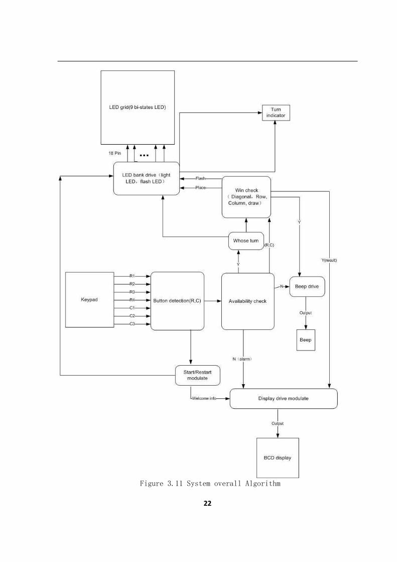
3.2. Software development 3.2.1. Clock module The overall structure of this design is as figure 3.11 illustrated. This design uses a
counter to divide the default frequence of 24 MHZ to get the Clock clk100 with a
frequence of 100 HZ. Clock Clkshake has a duty ratio of 50%, a counter is
employed to count the rising edge of clk, when it lays in [0,24000), clkshake is 1,
when it lays in [24000,48000],it is 0, which means half of the time it is 0, the
other half is 1.
3.2.2. Keypad driver In this design FSM(Finite State Machine) is used to program the keypad driver.
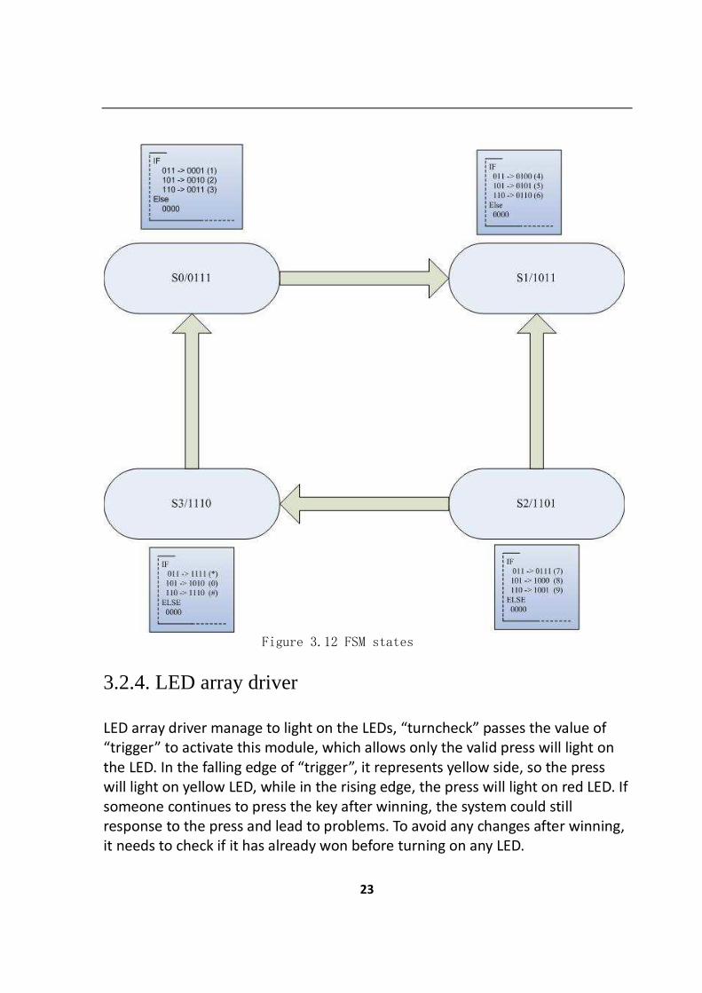
The states is as figure 3.12 shown, State st1 has 4 status s0 – s4, coded as 0111,
1011, 1110, 1101, each to represent the 1st
, 2nd
, 3rd
and 4th
row is low eletrical
level, other rows are high electrical level, before detecting any press, the state
machine keeps changing between the 4 states. If any key is pressed, the row and
column where the key locates will be connected to each other, then the column
turns to be low level, then it will be identified.
21
Then the keys need to be coded, i.e. when column is 011, 101, 110 or others,
combines it with the current state to encode. Like in state S0, when column is
011, then encode the key to be 0001. When column is 101, then encode the key
to be 0011, the same as the other 10 keys.
Then the driver need to remove jitter and double-click, add a 10ms delay when
detect press is simple but it could let to a slow keystoke. Especially for different
users who have different habbits of key pressing. The delay will not able to
satisfy all the user. There are many more complex and beautiful algrithms to
remove jitter. But limited to my understanding of VHDL, it is not easy to
accomplish it.
Then a compromising delay method is carried out, that is applying the delay to
LCD module instead of press detection module. Because LCD is a output device
helps player know the running status, it itself will not affect the function of
system. So even if it fails to remove the jitter, it will not lead to any system error,
compare to the possible miss detection in keypad, the consequence is relatively
slight.
3.2.3. Turn check Turn check module decides which side should play next. In this design, draw is
decided by counting the total number of turn change, so draw check is also
embedded in this module. By default, the yellow side play first, “turn_v” is 10,
“counter1” counts the rising edge of “turnchange”, when “counter1” is an even
number, “turn_v” is set 01, which means it is the red side’s turn to play. At the
same time, it checks if the number of “turnchange” has already reached 8 (9
steps at most in each play), if it is, set “draw” to be 1. When “counter1” is an odd
number, which means it is the turn of yellow side, then “turn_v” is back to “10”.
Due to the possible situation that one side wins at the last step, which satisfies
the condition of both win and draw, so before passing the value of “turn_v” to
the signal “turn” which binds to the physical output port.
22
Figure 3.11 System overall Algorithm
23
Figure 3.12 FSM states
3.2.4. LED array driver LED array driver manage to light on the LEDs, “turncheck” passes the value of
“trigger” to activate this module, which allows only the valid press will light on
the LED. In the falling edge of “trigger”, it represents yellow side, so the press
will light on yellow LED, while in the rising edge, the press will light on red LED. If
someone continues to press the key after winning, the system could still
response to the press and lead to problems. To avoid any changes after winning,
it needs to check if it has already won before turning on any LED.
24
3.2.5. Win check This module checks if either side has already won, it checks the three rows,
three columns and two diagonals of both sides and see if any of them has three
chessman. As there is 16 situations in total and each situation is easy to be
expressed, all the possibilities are simply enumerated in this design.
3.2.6. LED blink The module manages to blink the three LEDs in the winning line, as a clock with
duty ratio of 50% has already been defined, just assign this clock to LED will get
the result of 50% time on, 50% time off. LED driver and this blink module both
control the same LED array, so conflict is possible when turning on the last LED in
the winning line, in that case, none of the LEDs will blink when wins. So it needs
to check if it has already won before turn on any LEDs. If not, continue to turn it
on, otherwises, blink it.
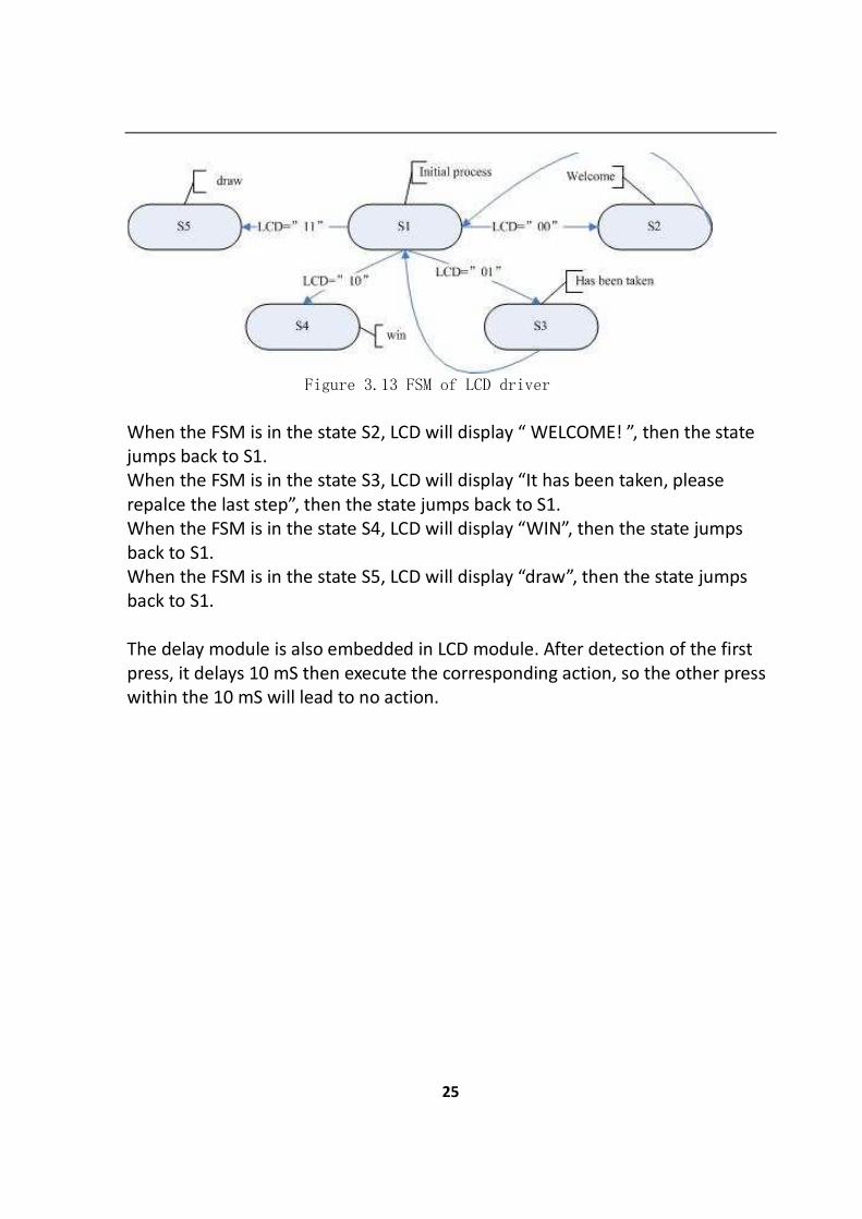
3.2.7. LCD driver This module manages the initial and display of LCD, in this design, it is also
accomplished by FSM, like figure 3.11 illustrated. There are S0,S1,S2,S3,S4,S5 UP
TO 6 states, the initial state is S0, it starts the LCD by executing the initial
commands in sequence. As the VHDL is a concurrent language, all the codes are
executed at the same time, so a counter is needed to make it sequential. After
initial, the state jumps to S1, this state checks condition to decide what the next
state is. When either “winr” or ”winy” is not 0, which means it has already won,
then jumps to S4. When both “winr” and ”winy” are 0 and “draw” equal to 1, i.e.
draw, jumps to S5. When neither win nor draw, if “takenup” is 1, that is press the
same key for more than one time, then jumps to S3. Otherwise, jumps to S2 to
shows welcome information.
25
Figure 3.13 FSM of LCD driver
When the FSM is in the state S2, LCD will display “ WELCOME! ”, then the state
jumps back to S1.
When the FSM is in the state S3, LCD will display “It has been taken, please
repalce the last step”, then the state jumps back to S1.
When the FSM is in the state S4, LCD will display “WIN”, then the state jumps
back to S1.
When the FSM is in the state S5, LCD will display “draw”, then the state jumps
back to S1.
The delay module is also embedded in LCD module. After detection of the first
press, it delays 10 mS then execute the corresponding action, so the other press
within the 10 mS will lead to no action.
26
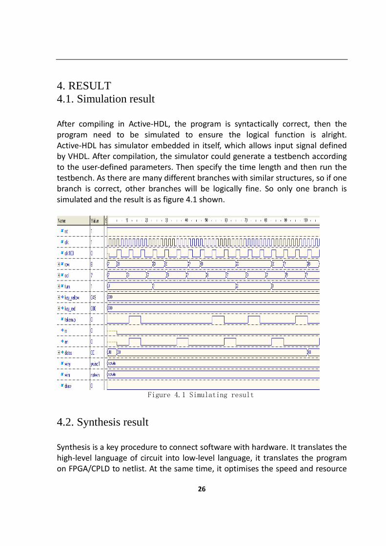
4. RESULT 4.1. Simulation result After compiling in Active-HDL, the program is syntactically correct, then the
program need to be simulated to ensure the logical function is alright.
Active-HDL has simulator embedded in itself, which allows input signal defined
by VHDL. After compilation, the simulator could generate a testbench according
to the user-defined parameters. Then specify the time length and then run the
testbench. As there are many different branches with similar structures, so if one
branch is correct, other branches will be logically fine. So only one branch is
simulated and the result is as figure 4.1 shown.
Figure 4.1 Simulating result
4.2. Synthesis result Synthesis is a key procedure to connect software with hardware. It translates the
high-level language of circuit into low-level language, it translates the program
on FPGA/CPLD to netlist. At the same time, it optimises the speed and resource
27
consumption of the program. Synthesis usually contains compilation, translation,
dispatch, assignment, synthesis and code generation. [11]
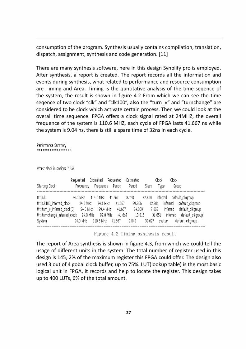
There are many synthesis software, here in this design Synplify pro is employed.
After synthesis, a report is created. The report records all the information and
events during synthesis, what related to performance and resource consumption
are Timing and Area. Timing is the quntitative analysis of the time seqence of
the system, the result is shown in figure 4.2 From which we can see the time
seqence of two clock “clk” and “clk100”, also the “turn_v” and “turnchange” are
considered to be clock which activate certain process. Then we could look at the
overall time sequence. FPGA offers a clock signal rated at 24MHZ, the overall
frequence of the system is 110.6 MHZ, each cycle of FPGA lasts 41.667 ns while
the system is 9.04 ns, there is still a spare time of 32ns in each cycle.
Figure 4.2 Timing synthesis result
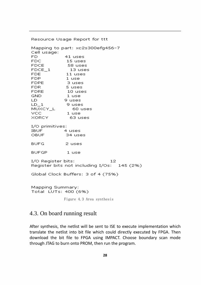
The report of Area synthesis is shown in figure 4.3, from which we could tell the
usage of different units in the system. The total number of register used in this
design is 145, 2% of the maximum register this FPGA could offer. The design also
used 3 out of 4 gobal clock buffer, up to 75%. LUT(lookup table) is the most basic
logical unit in FPGA, it records and help to locate the register. This design takes
up to 400 LUTs, 6% of the total amount.
28
Figure 4.3 Area synthesis
4.3. On board running result After synthesis, the netlist will be sent to ISE to execute implementation which
translate the netlist into bit file which could directly executed by FPGA. Then
download the bit file to FPGA using IMPACT. Choose boundary scan mode
through JTAG to burn onto PROM, then run the program.
29
5. CONCLUSION This design accomplishes two player Tic-Tac-Toe game on FPGA, it designs
circuits on experiment board, utilizes keypad as input, LED array and LCD as
output to represent Tic-Tac-Toe game. Then program in Active-HDL using VHDL
language, then synthesis in Synplify Pro to create netlist, then implement in ISE
developing suite to get executable bit file.
The main function of the design works properly, but there are still many possible
improvement which are not accomplished due to limited time and master of
VHDL language. Some of them are following:
The three keys in 4th row were not defined, so there are still expansion space.
It’s better to set the first key as reset key to replace the reset push button on
FPGA. The second key could be used as regret, it could be done by initial a stack
to record each step, when the key is pressed, pop out a step and remove it from
the chessboard array. The third key could be set as a switch between
human-computer, human-human mode.
This design defines human-human mode, if expand to human-computer mode, it
is related to AI, it is rather complex, which could probably beyond the computing
ability of this FPGA. But it is possible to encode one fixed way of playing into
FPGA. Like the first step of the player will have 9 possibilities, then encode the
response to these possibilities, they are fixed, one to one, the computer will only
follow a fixed way to play instead of making choice. There could be 8 choice
corresponding to each 9 different first steps, but it will always choose a fixed way,
thus, after the second step, there are still 9 situations. Then next step, it’s 7 and
so on. It’s up to 9*7*5*3*1 , 945 situation. In other words, it’s like the human
player is making decision and has at most up to 945 different choice. While
computer do not choose. According to WIKI, Ignoring the sequence of Xs and Os,
and after eliminating symmetrical outcomes (i.e. rotations and/or reflections of
other outcomes), there are only 138 unique outcomes. Assuming once again
that X makes the first move every time:
91 unique outcomes are won by (X)
44 unique outcomes are won by (O)
3 unique outcomes are drawn[12]
30
This 138 different outcomes are total possibilities, the total amount of solution
would vary depending on the strategy used, but definitely it will be less than 138.
So hard-coding all the possibilities may work.
31
REFERENCES:
[1] http://en.wikipedia.org/wiki/VHDL [2] http://en.wikipedia.org/wiki/Tic-tac-toe
[3] Xilinx, Spartan-IIE FPGA Family Data Sheet(1998)
[4] http://en.wikipedia.org/wiki/ActiveHDL [5]http://www.synopsys.com/Tools/Implementation/FPGAImplementation/FPG
ASynthesis/Pages/SynplifyPro.aspx
[6] http://en.wikipedia.org/wiki/Xilinx_ISE
[7] http://baike.baidu.com/view/1616079.html?fromTaglist
[8] http://baike.soso.com/v514379.htm
[9] http://ks.cn.yahoo.com/question/1306090907561.html
[10] OPTREX CORPORATION, DMC16207N LCD Module Specification(1999)
[11] http://wenku.baidu.com/view/e04a7124ccbff121dd3683e8.html
[12] http://en.wikipedia.org/wiki/Tic-tac-toe#Number_of_possible_games
32
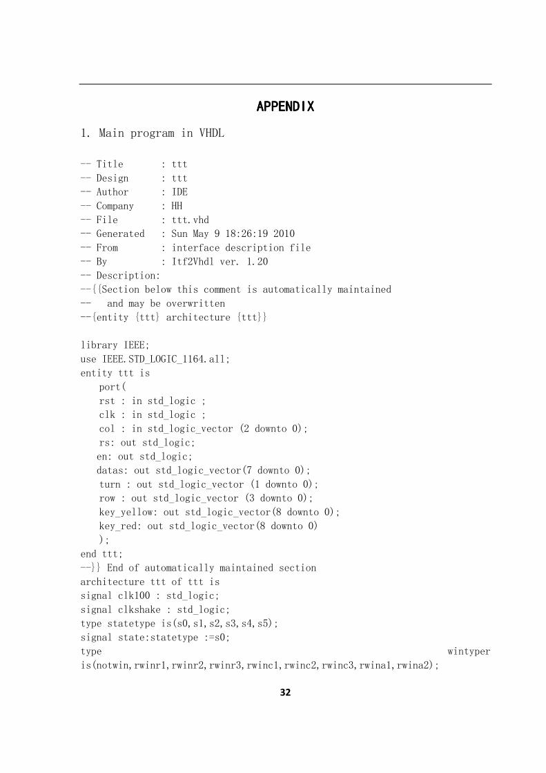
APPENDIXAPPENDIXAPPENDIXAPPENDIX
1. Main program in VHDL
-- Title : ttt
-- Design : ttt
-- Author : IDE
-- Company : HH
-- File : ttt.vhd
-- Generated : Sun May 9 18:26:19 2010
-- From : interface description file
-- By : Itf2Vhdl ver. 1.20
-- Description:
--{{Section below this comment is automatically maintained
-- and may be overwritten
--{entity {ttt} architecture {ttt}}
library IEEE;
use IEEE.STD_LOGIC_1164.all;
entity ttt is
port(
rst : in std_logic ;
clk : in std_logic ;
col : in std_logic_vector (2 downto 0);
rs: out std_logic;
en: out std_logic;
datas: out std_logic_vector(7 downto 0);
turn : out std_logic_vector (1 downto 0);
row : out std_logic_vector (3 downto 0);
key_yellow: out std_logic_vector(8 downto 0);
key_red: out std_logic_vector(8 downto 0)
);
end ttt;
--}} End of automatically maintained section
architecture ttt of ttt is
signal clk100 : std_logic;
signal clkshake : std_logic;
type statetype is(s0,s1,s2,s3,s4,s5);
signal state:statetype :=s0;
type wintyper
is(notwin,rwinr1,rwinr2,rwinr3,rwinc1,rwinc2,rwinc3,rwina1,rwina2);
33
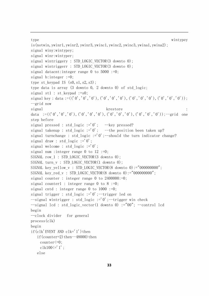
type wintypey
is(notwin,ywinr1,ywinr2,ywinr3,ywinc1,ywinc2,ywinc3,ywina1,ywina2);
signal winy:wintypey;
signal winr:wintyper;
signal wintriggery : STD_LOGIC_VECTOR(3 downto 0);
signal wintriggerr : STD_LOGIC_VECTOR(3 downto 0);
signal datacnt:integer range 0 to 5000 :=0;
signal b:integer :=0;
type st_keypad IS (s0,s1,s2,s3);
type data is array (3 downto 0, 2 downto 0) of std_logic;
signal st1 : st_keypad :=s0;
signal key : data :=(('0','0','0'),('0','0','0'),('0','0','0'),('0','0','0'));
--grid now
signal krestore :
data :=(('0','0','0'),('0','0','0'),('0','0','0'),('0','0','0'));--grid one
step before
signal pressed : std_logic :='0'; --key pressed?
signal takenup : std_logic :='0'; --the position been taken up?
signal turnchange : std_logic :='0';--should the turn indicator change?
signal draw : std_logic :='0';
signal welcome : std_logic :='0';
signal num :integer range 0 to 12 :=0;
SIGNAL row_1 : STD_LOGIC_VECTOR(3 downto 0);
SIGNAL turn_v : STD_LOGIC_VECTOR(1 downto 0);
SIGNAL key_yellow_v : STD_LOGIC_VECTOR(8 downto 0):="000000000";
SIGNAL key_red_v : STD_LOGIC_VECTOR(8 downto 0):="000000000";
signal counter : integer range 0 to 2400000:=0;
signal counter1 : integer range 0 to 8 :=0;
signal cntd : integer range 0 to 1000 :=0;
signal trigger : std_logic :='0';--trigger led on
--signal wintrigger : std_logic :='0';--trigger win check
--signal lcd : std_logic_vector(1 downto 0) :="00"; --control lcd
begin
--clock divider for general
process(clk)
begin
if(clk'EVENT AND clk='1')then
if(counter=2)then--48000)then
counter<=0;
clk100<='1';
else
34
counter<=counter+1;
clk100<='0';
end if;
end if;
end process;
--clock divider for led sparkling
process(clk)
variable counter2 : integer range 0 to 4800000;
begin
if(clk'event and clk='1') then
if(counter2 = 4)then--4800000) then
counter2 := 0 ;
else counter2 := counter2 + 1 ;
if(counter2 < 2)then--2400000) then
clkshake <= '0' ;
else clkshake <= '1' ;
end if ;
end if ;
end if ;
end process ;
--keypad
----------------------------------------------------------------------------
----------------------------------------------------------------------------
-------------------
process(clk100,rst)
begin
if(rst='0')then
key<=(('0','0','0'),('0','0','0'),('0','0','0'),('0','0','0'));
krestore<=(('0','0','0'),('0','0','0'),('0','0','0'),('0','0','0'));
pressed<='0';
turnchange<='0';
st1<=s0;
num<=0;
takenup<='0';
elsif(clk100'EVENT AND clk100='1')then
case st1 IS
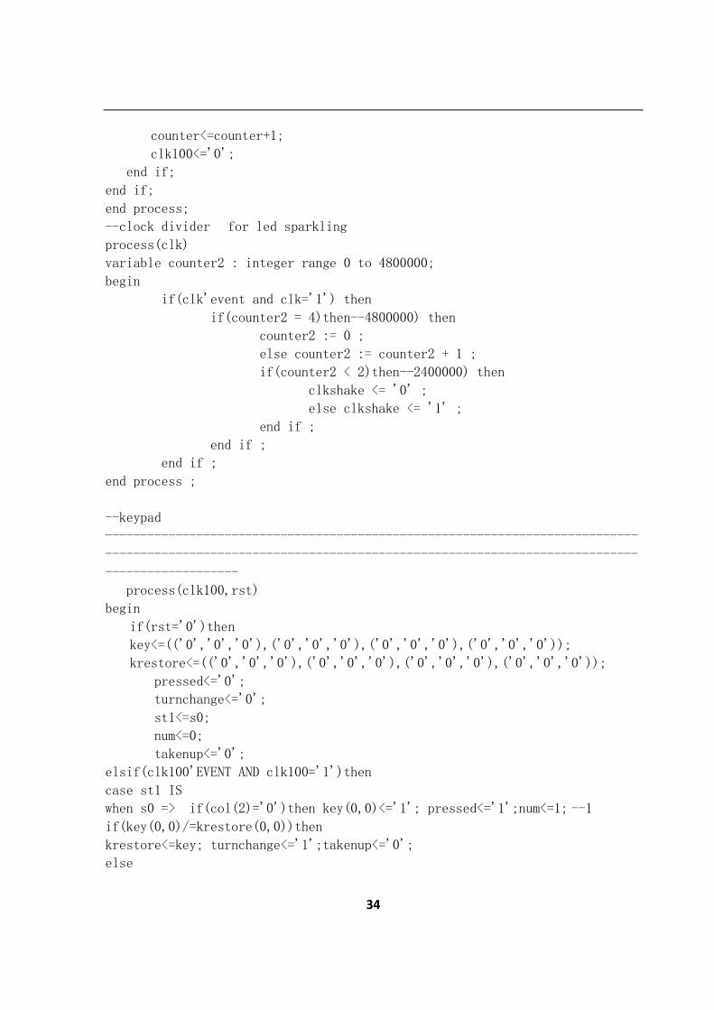
when s0 => if(col(2)='0')then key(0,0)<='1'; pressed<='1';num<=1; --1
if(key(0,0)/=krestore(0,0))then
krestore<=key; turnchange<='1';takenup<='0';
else
35
takenup<='1';turnchange<='0';
end if;
elsif(col(1)='0')then key(0,1)<='1'; pressed<='1';num<=2; --2
if (key(0,1)/= krestore(0,1))then
krestore<=key;
turnchange<='1';takenup<='0';
else
takenup<='1';turnchange<='0';
end if;
elsif(col(0)='0')then key(0,2)<='1'; pressed<='1';num<=3; --3
if (key(0,2)/= krestore(0,2))then
krestore<=key; turnchange<='1';takenup<='0';
else
takenup<='1';turnchange<='0';
end if;
else
st1<=s1; pressed<='0';turnchange<='0';num<=0;takenup<='0';
end if;
when s1 => if(col(2)='0')then key(1,0)<='1';pressed<='1';num<=4; --4
if (key(1,0)/= krestore(1,0))then
krestore<=key; turnchange<='1';takenup<='0';
else
takenup<='1';turnchange<='0';
end if;
elsif(col(1)='0')then key(1,1)<='1'; pressed<='1';num<=5; --5
if (key(1,1)/= krestore(1,1))then
krestore<=key; turnchange<='1';takenup<='0';
else
takenup<='1';turnchange<='0';
end if;
elsif(col(0)='0')then key(1,2)<='1'; pressed<='1'; num<=6;--6
if (key(1,2)/= krestore(1,2))then
krestore<=key; turnchange<='1'; takenup<='0';
else
takenup<='1';turnchange<='0';
end if;
else
st1<=s2; pressed<='0';turnchange<='0';num<=0; takenup<='0';
end if;
when s2 => if(col(2)='0')then key(2,0)<='1'; pressed<='1'; num<=7; --7
36
if (key(2,0)/= krestore(2,0))then
krestore<=key;
turnchange<='1';takenup<='0';
else
takenup<='1';turnchange<='0';
end if;
elsif(col(1)='0')then key(2,1)<='1'; pressed<='1';num<=8; --8
if (key(2,1)/= krestore(2,1))then
krestore<=key;
turnchange<='1';takenup<='0';
else
takenup<='1';turnchange<='0';
end if;
elsif(col(0)='0')then key(2,2)<='1'; pressed<='1';num<=9; --9
if (key(2,2)/= krestore(2,2))then
krestore<=key; turnchange<='1'; takenup<='0';
else
takenup<='1';turnchange<='0';
end if;
else st1<=s3; pressed<='0'; turnchange<='0'; num<=0; takenup<='0';
end if;
when s3 =>
if(col(2)='0')then
key(3,0)<='1'; pressed<='1';turnchange<='0';num<=10; --*
elsif(col(1)='0')then
key(3,1)<='1'; pressed<='1';turnchange<='0';num<=11; --0
elsif(col(0)='0')then
key(3,2)<='1'; pressed<='1';turnchange<='0';num<=12; --#
else st1<=s0;pressed<='0'; turnchange<='0'; num<=0;
end if;
When others => st1<=s0; num<=0;takenup<='0';
end case;
end if;
end process;
row<=row_1;
--col combination
process(st1)
begin
case st1 is
when s0 => row_1<="0111";
37
when s1 => row_1<="1011";
when s2 => row_1<="1101";
when s3 => row_1<="1110";
end case;
end process;
----------------------------------------------------------------------------
--------------------------------------
--turn check (and draw check)
process(turnchange,rst)
begin
if (rst='0')then
turn_v<="10"; counter1<=0;trigger<='0';draw<='0';--yellow first
elsif( turnchange'event and turnchange='1') then
counter1<=counter1+1;
if (counter1 mod 2 =0) then turn_v<="01";trigger<='1';
if (counter1 = 8)then
draw<='1';
else draw<='0';
end if;
elsif (counter1 mod 2=1) then turn_v<="10";trigger<='0';
else
null;
end if ;
else
null;
end if ;
end process;
process(clk100)
begin
if (clk100'event and clk100='1')then
if(winr=notwin and winy=notwin) then
turn<=turn_v;
else null;
end if;
else null;
end if;
end process;
----------------------------------------------------------------------------
--------------------------------------
--LED on (wintrigger?????????????)
process(trigger,rst)
38
begin
if (rst='0')then
key_yellow_v<="000000000";
wintriggery <="0000";
elsif(trigger'event and trigger='1') then
if(winy=notwin and winr=notwin) then
case num is
when 1=> key_yellow_v(0)<='1';wintriggery<="0001";
when 2=> key_yellow_v(1)<='1';wintriggery<="0010";
when 3=> key_yellow_v(2)<='1';wintriggery<="0011";
when 4=> key_yellow_v(3)<='1';wintriggery<="0100";
when 5=> key_yellow_v(4)<='1';wintriggery<="0101";
when 6=> key_yellow_v(5)<='1';wintriggery<="0110";
when 7=> key_yellow_v(6)<='1';wintriggery<="0111";
when 8=> key_yellow_v(7)<='1';wintriggery<="1000";
when 9=> key_yellow_v(8)<='1';wintriggery<="1001";
when others => wintriggery<="0000";
end case;
else null;
end if;
else null;
end if;
end process;
process(trigger,rst)
begin
if (rst='0')then --"trigger" : a trigger generated by
turncheck to indicate which side it is now
key_red_v <="000000000";
wintriggerr <="0000";
elsif(trigger'event and trigger='0') then
if(winr=notwin and winy=notwin) then
case num is
when 1=> key_red_v(0)<='1';wintriggerr<="0001";
when 2=> key_red_v(1)<='1';wintriggerr<="0010";
when 3=> key_red_v(2)<='1';wintriggerr<="0011";
when 4=> key_red_v(3)<='1';wintriggerr<="0100";
when 5=> key_red_v(4)<='1';wintriggerr<="0101";
when 6=> key_red_v(5)<='1';wintriggerr<="0110";
when 7=> key_red_v(6)<='1';wintriggerr<="0111";
when 8=> key_red_v(7)<='1';wintriggerr<="1000";
when 9=> key_red_v(8)<='1';wintriggerr<="1001";
39
when others => wintriggerr<="0000";
end case;
else null;
end if;
else null;
end if;
end process;
----------------------------------------------------------------------------
--------------------------------------
------win check (key_v and wins?????????????)
process(clk100,rst)
begin
if (rst='0')then
winy<=notwin;
elsif(clk100'event and clk100='1') then
if(wintriggerr /= "0000" )then
if((key_yellow_v(0)='1') and (key_yellow_v(1)='1') and
(key_yellow_v(2)='1'))then winy<=ywinr1;
elsif((key_yellow_v(3)='1') and (key_yellow_v(4)='1') and
(key_yellow_v(5)='1'))then winy<=ywinr2;
elsif((key_yellow_v(6)='1') and (key_yellow_v(7)='1') and
(key_yellow_v(8)='1'))then winy<=ywinr3;
elsif((key_yellow_v(0)='1') and (key_yellow_v(3)='1') and
(key_yellow_v(6)='1')) then winy<=ywinc1;
elsif((key_yellow_v(1)='1') and (key_yellow_v(4)='1') and
(key_yellow_v(7)='1')) then winy<=ywinc2;
elsif((key_yellow_v(2)='1') and (key_yellow_v(5)='1') and
(key_yellow_v(8)='1')) then winy<=ywinc3;
elsif((key_yellow_v(0)='1') and (key_yellow_v(4)='1') and
(key_yellow_v(8)='1')) then winy<=ywina1;
elsif((key_yellow_v(2)='1') and (key_yellow_v(4)='1') and
(key_yellow_v(6)='1')) then winy<=ywina2;
else
winy<=notwin;
end if;
else null;
end if;
else null;
end if;
end process ;
process(clk100,rst)
40
begin
if (rst='0')then
winr<= notwin;
elsif(clk100'event and clk100='1') then
if(wintriggerr /= "0000" )then
if( key_red_v(0)='1' and key_red_v(1)='1' and key_red_v(2)='1') then
winr<=rwinr1;
elsif(key_red_v(3)='1' and key_red_v(4)='1' and key_red_v(5)='1') then
winr<=rwinr2;
elsif(key_red_v(6)='1' and key_red_v(7)='1' and key_red_v(8)='1') then
winr<=rwinr3;
elsif(key_red_v(0)='1' and key_red_v(3)='1' and key_red_v(6)='1') then
winr<=rwinc1;
elsif(key_red_v(1)='1' and key_red_v(4)='1' and key_red_v(7)='1') then
winr<=rwinc2;
elsif(key_red_v(2)='1' and key_red_v(5)='1' and key_red_v(8)='1') then
winr<=rwinc3;
elsif(key_red_v(0)='1' and key_red_v(4)='1' and key_red_v(8)='1') then
winr<=rwina1;
elsif(key_red_v(2)='1' and key_red_v(4)='1' and key_red_v(6)='1') then
winr<=rwina2;
else
winr<=notwin;
end if;
else null;
end if;
else null;
end if;
end process ;
----------------------------------------------------------------------------
--------------------------------------
--led sparkling(too many if, wins ???????)
process(winr)
begin
case winr is
when rwinr1 =>
key_red(0)<=clkshake;
key_red(1)<=clkshake;
key_red(2)<=clkshake;
when rwinr2 =>
key_red(3)<=clkshake;
41
key_red(4)<=clkshake;
key_red(5)<=clkshake;
when rwinr3 =>
key_red(6)<=clkshake;
key_red(7)<=clkshake;
key_red(8)<=clkshake;
when rwinc1 =>
key_red(0)<=clkshake;
key_red(3)<=clkshake;
key_red(6)<=clkshake;
when rwinc2 =>
key_red(1)<=clkshake;
key_red(4)<=clkshake;
key_red(7)<=clkshake;
when rwinc3 =>
key_red(2)<=clkshake;
key_red(5)<=clkshake;
key_red(8)<=clkshake;
when rwina1 =>
key_red(0)<=clkshake;
key_red(4)<=clkshake;
key_red(8)<=clkshake;
when rwina2 =>
key_red(2)<=clkshake;
key_red(4)<=clkshake;
key_red(6)<=clkshake;
when notwin=>
key_red<=key_red_v;
when others =>null;
end case;
end process;
process(winy)
begin
case winy is
when ywinr1 =>
key_yellow(0)<=clkshake;
key_yellow(1)<=clkshake;
key_yellow(2)<=clkshake;
when ywinr2 =>
key_yellow(3)<=clkshake;
key_yellow(4)<=clkshake;
42
key_yellow(5)<=clkshake;
when ywinr3 =>
key_yellow(6)<=clkshake;
key_yellow(7)<=clkshake;
key_yellow(8)<=clkshake;
when ywinc1 =>
key_yellow(0)<=clkshake;
key_yellow(3)<=clkshake;
key_yellow(6)<=clkshake;
when ywinc2 =>
key_yellow(1)<=clkshake;
key_yellow(4)<=clkshake;
key_yellow(7)<=clkshake;
when ywinc3 =>
key_yellow(2)<=clkshake;
key_yellow(5)<=clkshake;
key_yellow(8)<=clkshake;
when ywina1 =>
key_yellow(0)<=clkshake;
key_yellow(4)<=clkshake;
key_yellow(8)<=clkshake;
when ywina2 =>
key_yellow(2)<=clkshake;
key_yellow(4)<=clkshake;
key_yellow(6)<=clkshake;
when notwin=>
key_yellow<=key_yellow_v ;
when others =>null;
end case;
end process;
----------------------------------------------------------------------------
--------------------------------------
--LCD configuration
process(rst,clk100)
begin
if(rst='0')then
en<='0';
rs<='0';
datacnt<=0;
state<=s0;
welcome<='0';
43
elsif (clk100'EVENT AND clk100='1') then
case state is
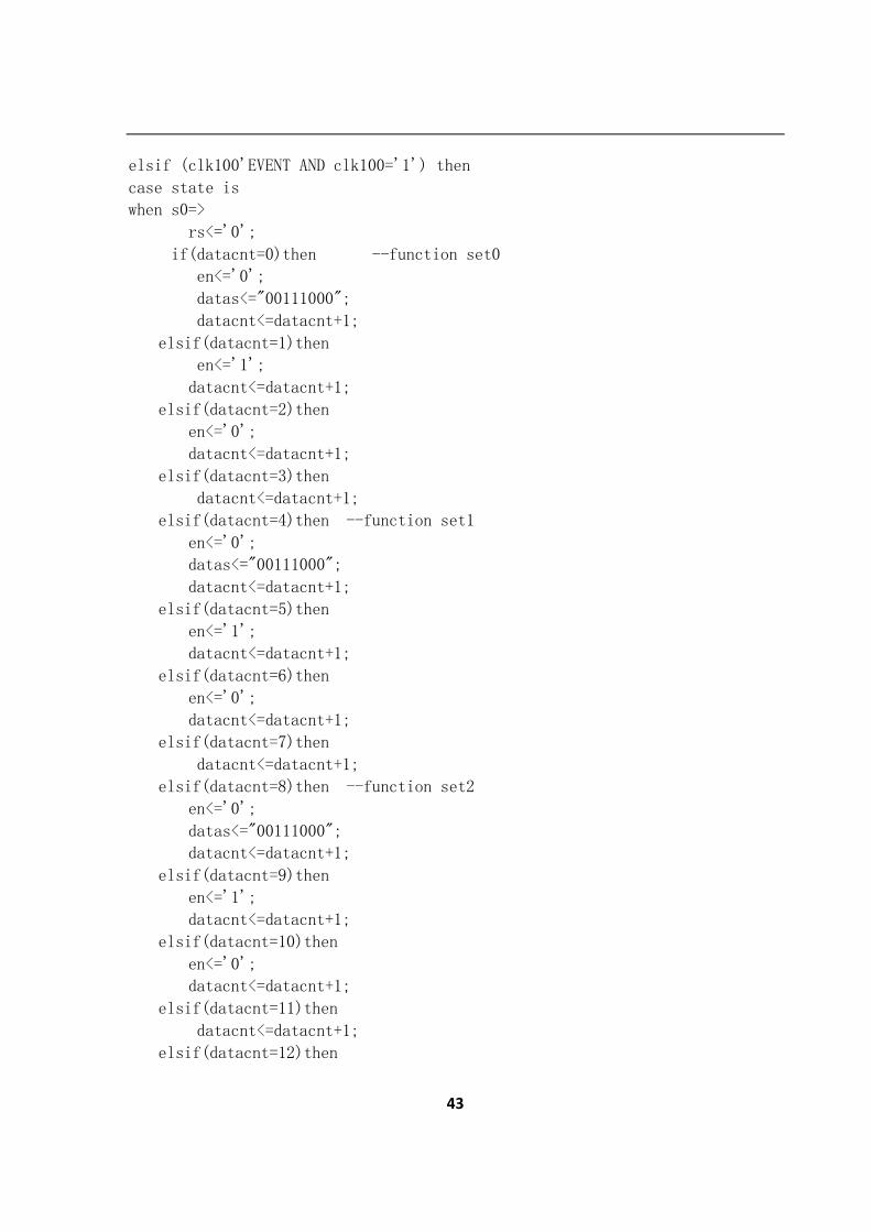
when s0=>
rs<='0';
if(datacnt=0)then --function set0
en<='0';
datas<="00111000";
datacnt<=datacnt+1;
elsif(datacnt=1)then
en<='1';
datacnt<=datacnt+1;
elsif(datacnt=2)then
en<='0';
datacnt<=datacnt+1;
elsif(datacnt=3)then
datacnt<=datacnt+1;
elsif(datacnt=4)then --function set1
en<='0';
datas<="00111000";
datacnt<=datacnt+1;
elsif(datacnt=5)then
en<='1';
datacnt<=datacnt+1;
elsif(datacnt=6)then
en<='0';
datacnt<=datacnt+1;
elsif(datacnt=7)then
datacnt<=datacnt+1;
elsif(datacnt=8)then --function set2
en<='0';
datas<="00111000";
datacnt<=datacnt+1;
elsif(datacnt=9)then
en<='1';
datacnt<=datacnt+1;
elsif(datacnt=10)then
en<='0';
datacnt<=datacnt+1;
elsif(datacnt=11)then
datacnt<=datacnt+1;
elsif(datacnt=12)then
44
en<='0';
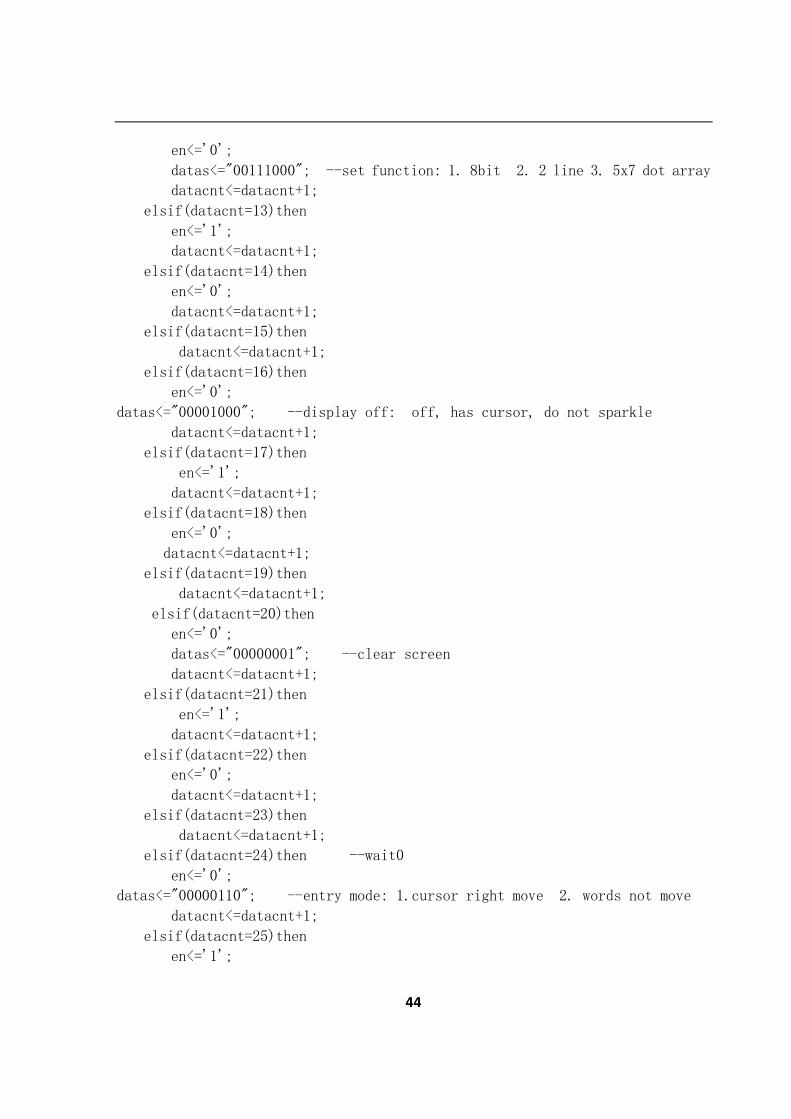
datas<="00111000"; --set function: 1. 8bit 2. 2 line 3. 5x7 dot array
datacnt<=datacnt+1;
elsif(datacnt=13)then
en<='1';
datacnt<=datacnt+1;
elsif(datacnt=14)then
en<='0';
datacnt<=datacnt+1;
elsif(datacnt=15)then
datacnt<=datacnt+1;
elsif(datacnt=16)then
en<='0';
datas<="00001000"; --display off: off, has cursor, do not sparkle
datacnt<=datacnt+1;
elsif(datacnt=17)then
en<='1';
datacnt<=datacnt+1;
elsif(datacnt=18)then
en<='0';
datacnt<=datacnt+1;
elsif(datacnt=19)then
datacnt<=datacnt+1;
elsif(datacnt=20)then
en<='0';
datas<="00000001"; --clear screen
datacnt<=datacnt+1;
elsif(datacnt=21)then
en<='1';
datacnt<=datacnt+1;
elsif(datacnt=22)then
en<='0';
datacnt<=datacnt+1;
elsif(datacnt=23)then
datacnt<=datacnt+1;
elsif(datacnt=24)then --wait0
en<='0';
datas<="00000110"; --entry mode: 1.cursor right move 2. words not move
datacnt<=datacnt+1;
elsif(datacnt=25)then
en<='1';
45
datacnt<=datacnt+1;
elsif(datacnt=26)then --wait1
en<='0';
datacnt<=datacnt+1;
elsif(datacnt=27)then
datacnt<=datacnt+1;
elsif(datacnt=28)then
en<='0'; --wait0
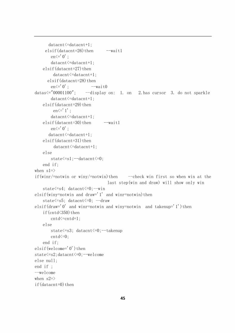
datas<="00001100"; --display on: 1. on 2.has cursor 3. do not sparkle
datacnt<=datacnt+1;
elsif(datacnt=29)then
en<='1';
datacnt<=datacnt+1;
elsif(datacnt=30)then --wait1
en<='0';
datacnt<=datacnt+1;
elsif(datacnt=31)then
datacnt<=datacnt+1;
else
state<=s1;--datacnt<=0;
end if;
when s1=>
if(winr/=notwin or winy/=notwin)then --check win first so when win at the
last step(win and draw) will show only win
state<=s4; datacnt<=0;--win
elsif(winy=notwin and draw='1' and winr=notwin)then
state<=s5; datacnt<=0; --draw
elsif(draw='0' and winr=notwin and winy=notwin and takenup='1')then
if(cntd<350)then
cntd<=cntd+1;
else
state<=s3; datacnt<=0;--takenup
cntd<=0;
end if;
elsif(welcome='0')then
state<=s2;datacnt<=0;--welcome
else null;
end if ;
--welcome
when s2=>
if(datacnt=0)then
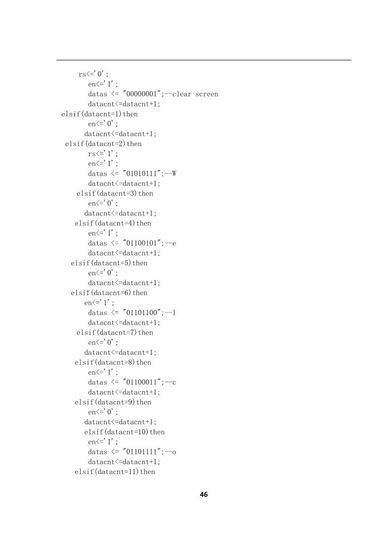
46
rs<='0';
en<='1';
datas <= "00000001";--clear screen
datacnt<=datacnt+1;
elsif(datacnt=1)then
en<='0';
datacnt<=datacnt+1;
elsif(datacnt=2)then
rs<='1';
en<='1';
datas <= "01010111";--W
datacnt<=datacnt+1;
elsif(datacnt=3)then
en<='0';
datacnt<=datacnt+1;
elsif(datacnt=4)then
en<='1';
datas <= "01100101";--e
datacnt<=datacnt+1;
elsif(datacnt=5)then
en<='0';
datacnt<=datacnt+1;
elsif(datacnt=6)then
en<='1';
datas <= "01101100";--l
datacnt<=datacnt+1;
elsif(datacnt=7)then
en<='0';
datacnt<=datacnt+1;
elsif(datacnt=8)then
en<='1';
datas <= "01100011";--c
datacnt<=datacnt+1;
elsif(datacnt=9)then
en<='0';
datacnt<=datacnt+1;
elsif(datacnt=10)then
en<='1';
datas <= "01101111";--o
datacnt<=datacnt+1;
elsif(datacnt=11)then
47
en<='0';
datacnt<=datacnt+1;
elsif(datacnt=12)then
en<='1';
datas <= "01101101";--m
datacnt<=datacnt+1;
elsif(datacnt=13)then
en<='0';
datacnt<=datacnt+1;
elsif(datacnt=14)then
en<='1';
datas <= "01100101";--e
datacnt<=datacnt+1;
elsif(datacnt=15)then
en<='0';
datacnt<=datacnt+1;
elsif(datacnt=16)then
en<='1';
datas <= "00100001";--!
datacnt<=datacnt+1;
elsif(datacnt=17)then
en<='0';
datacnt<=datacnt+1;
else
state<=s1; welcome<='1';
end if;
--taken up
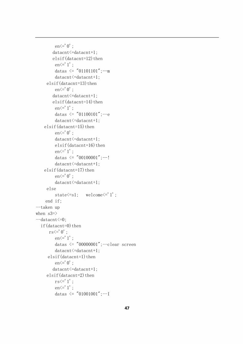
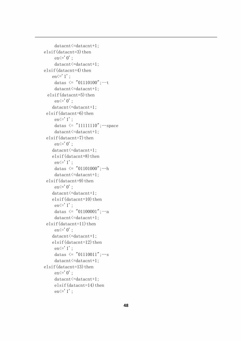
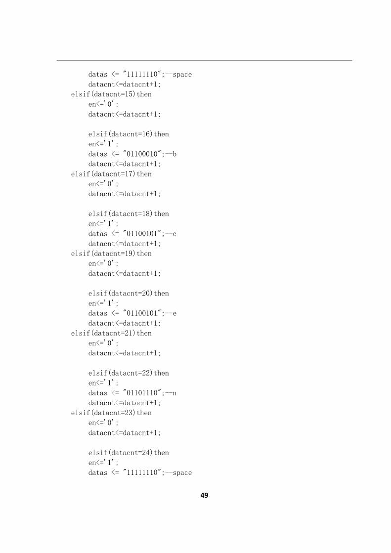
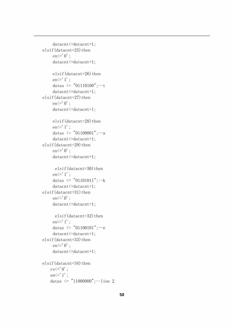
when s3=>
--datacnt<=0;
if(datacnt=0)then
rs<='0';
en<='1';
datas <= "00000001";--clear screen
datacnt<=datacnt+1;
elsif(datacnt=1)then
en<='0';
datacnt<=datacnt+1;
elsif(datacnt=2)then
rs<='1';
en<='1';
datas <= "01001001";--I
48
datacnt<=datacnt+1;
elsif(datacnt=3)then
en<='0';
datacnt<=datacnt+1;
elsif(datacnt=4)then
en<='1';
datas <= "01110100";--t
datacnt<=datacnt+1;
elsif(datacnt=5)then
en<='0';
datacnt<=datacnt+1;
elsif(datacnt=6)then
en<='1';
datas <= "11111110";--space
datacnt<=datacnt+1;
elsif(datacnt=7)then
en<='0';
datacnt<=datacnt+1;
elsif(datacnt=8)then
en<='1';
datas <= "01101000";--h
datacnt<=datacnt+1;
elsif(datacnt=9)then
en<='0';
datacnt<=datacnt+1;
elsif(datacnt=10)then
en<='1';
datas <= "01100001";--a
datacnt<=datacnt+1;
elsif(datacnt=11)then
en<='0';
datacnt<=datacnt+1;
elsif(datacnt=12)then
en<='1';
datas <= "01110011";--s
datacnt<=datacnt+1;
elsif(datacnt=13)then
en<='0';
datacnt<=datacnt+1;
elsif(datacnt=14)then
en<='1';
49
datas <= "11111110";--space
datacnt<=datacnt+1;
elsif(datacnt=15)then
en<='0';
datacnt<=datacnt+1;
elsif(datacnt=16)then
en<='1';
datas <= "01100010";--b
datacnt<=datacnt+1;
elsif(datacnt=17)then
en<='0';
datacnt<=datacnt+1;
elsif(datacnt=18)then
en<='1';
datas <= "01100101";--e
datacnt<=datacnt+1;
elsif(datacnt=19)then
en<='0';
datacnt<=datacnt+1;
elsif(datacnt=20)then
en<='1';
datas <= "01100101";--e
datacnt<=datacnt+1;
elsif(datacnt=21)then
en<='0';
datacnt<=datacnt+1;
elsif(datacnt=22)then
en<='1';
datas <= "01101110";--n
datacnt<=datacnt+1;
elsif(datacnt=23)then
en<='0';
datacnt<=datacnt+1;
elsif(datacnt=24)then
en<='1';
datas <= "11111110";--space
50
datacnt<=datacnt+1;
elsif(datacnt=25)then
en<='0';
datacnt<=datacnt+1;
elsif(datacnt=26)then
en<='1';
datas <= "01110100";--t
datacnt<=datacnt+1;
elsif(datacnt=27)then
en<='0';
datacnt<=datacnt+1;
elsif(datacnt=28)then
en<='1';
datas <= "01100001";--a
datacnt<=datacnt+1;
elsif(datacnt=29)then
en<='0';
datacnt<=datacnt+1;
elsif(datacnt=30)then
en<='1';
datas <= "01101011";--k
datacnt<=datacnt+1;
elsif(datacnt=31)then
en<='0';
datacnt<=datacnt+1;
elsif(datacnt=32)then
en<='1';
datas <= "01100101";--e
datacnt<=datacnt+1;
elsif(datacnt=33)then
en<='0';
datacnt<=datacnt+1;
elsif(datacnt=34)then
rs<='0';
en<='1';
datas <= "11000000";--line 2
51
datacnt<=datacnt+1;
elsif(datacnt=35)then
en<='0';
datacnt<=datacnt+1;
elsif(datacnt=36)then
rs<='1';
en<='1';
datas <= "01101110";--n
datacnt<=datacnt+1;
elsif(datacnt=37)then
en<='0';
datacnt<=datacnt+1;
elsif(datacnt=38)then
en<='1';
datas <= "11111110";--space
datacnt<=datacnt+1;
elsif(datacnt=39)then
en<='0';
datacnt<=datacnt+1;
elsif(datacnt=40)then
en<='1';
datas <= "01110000";--p
datacnt<=datacnt+1;
elsif(datacnt=41)then
en<='0';
datacnt<=datacnt+1;
elsif(datacnt=42)then
en<='1';
datas <= "01101100";--l
datacnt<=datacnt+1;
elsif(datacnt=43)then
en<='0';
datacnt<=datacnt+1;
elsif(datacnt=44)then
en<='1';
datas <= "01100101";--e
52
datacnt<=datacnt+1;
elsif(datacnt=45)then
en<='0';
datacnt<=datacnt+1;
elsif(datacnt=46)then
en<='1';
datas <= "01100001";--a
datacnt<=datacnt+1;
elsif(datacnt=47)then
en<='0';
datacnt<=datacnt+1;
elsif(datacnt=48)then
en<='1';
datas <= "01110011";--s
datacnt<=datacnt+1;
elsif(datacnt=49)then
en<='0';
datacnt<=datacnt+1;
elsif(datacnt=50)then
en<='1';
datas <= "01100101";--e
datacnt<=datacnt+1;
elsif(datacnt=51)then
en<='0';
datacnt<=datacnt+1;
elsif(datacnt=52)then
en<='1';
datas <= "11111110";--space
datacnt<=datacnt+1;
elsif(datacnt=53)then
en<='0';
datacnt<=datacnt+1;
elsif(datacnt=54)then
en<='1';
datas <= "01110010";--r
datacnt<=datacnt+1;
53
elsif(datacnt=55)then
en<='0';
datacnt<=datacnt+1;
elsif(datacnt=56)then
en<='1';
datas <= "01100101";--e
datacnt<=datacnt+1;
elsif(datacnt=57)then
en<='0';
datacnt<=datacnt+1;
elsif(datacnt=58)then
en<='1';
datas <= "01110000";--p
datacnt<=datacnt+1;
elsif(datacnt=59)then
en<='0';
datacnt<=datacnt+1;
elsif(datacnt=60)then
en<='1';
datas <= "01101100";--l
datacnt<=datacnt+1;
elsif(datacnt=61)then
en<='0';
datacnt<=datacnt+1;
elsif(datacnt=62)then
en<='1';
datas <= "01100001";--a
datacnt<=datacnt+1;
elsif(datacnt=63)then
en<='0';
datacnt<=datacnt+1;
elsif(datacnt=64)then
en<='1';
datas <= "01100011";--c
datacnt<=datacnt+1;
elsif(datacnt=65)then
54
en<='0';
datacnt<=datacnt+1;
elsif(datacnt=66)then
en<='1';
datas <= "01100101";--e
datacnt<=datacnt+1;
elsif(datacnt=67)then
en<='0';
datacnt<=datacnt+1;
elsif(datacnt<500)then
datacnt<=datacnt+1;
else
state<=s1;welcome<='0';
end if;
--win
when s4=>
--datacnt<=0;
if(datacnt=0)then
rs<='0';
en<='1';
datas <= "00000001";--clear screen
datacnt<=datacnt+1;
elsif(datacnt=1)then
en<='0';
datacnt<=datacnt+1;
elsif(datacnt=2)then
rs<='1';
en<='1';
datas <= "01010111";--W
datacnt<=datacnt+1;
elsif(datacnt=3)then
en<='0';
datacnt<=datacnt+1;
elsif(datacnt=4)then
en<='1';
datas <= "01101001";--i
datacnt<=datacnt+1;
55
elsif(datacnt=5)then
en<='0';
datacnt<=datacnt+1;
elsif(datacnt=6)then
en<='1';
datas <= "01101110";--n
datacnt<=datacnt+1;
elsif(datacnt=7)then
en<='0';
datacnt<=datacnt+1;
elsif(datacnt=8)then
en<='1';
datas <= "00100001";--!
datacnt<=datacnt+1;
elsif(datacnt=9)then
en<='0';
datacnt<=datacnt+1;
else
welcome<='0';
end if;
--draw
when s5=>
if(datacnt=0)then
rs<='0';
en<='1';
datas <= "00000001";--clear screen
datacnt<=datacnt+1;
elsif(datacnt=1)then
en<='0';
datacnt<=datacnt+1;
elsif(datacnt=2)then
rs<='1';
en<='1';
datas <= "01100100";--d
datacnt<=datacnt+1;
elsif(datacnt=3)then
en<='0';
datacnt<=datacnt+1;
56
elsif(datacnt=4)then
en<='1';
datas <= "01110010";--r
datacnt<=datacnt+1;
elsif(datacnt=5)then
en<='0';
datacnt<=datacnt+1;
elsif(datacnt=6)then
en<='1';
datas <= "01100001";--a
datacnt<=datacnt+1;
elsif(datacnt=7)then
en<='0';
datacnt<=datacnt+1;
elsif(datacnt=8)then
en<='1';
datas <= "01010111";--w
datacnt<=datacnt+1;
elsif(datacnt=9)then
en<='0';
datacnt<=datacnt+1;
else
welcome<='0';
end if;
when others=>state<=s0;
end case;
end if;
end process;
end ttt;
2. Pin description file
NET "clk" LOC ="C11";
NET "rst" LOC ="A6";
net turn(0) loc="T5";
net turn(1) loc="P5";
57
NET col(0) LOC = "G5";
NET col(1) LOC = "C2";
NET col(2) LOC = "F5";
NET row(0) LOC = "N2";
NET row(1) LOC = "N1";
NET row(2) LOC = "M2";
NET row(3) LOC = "M1";
NET key_yellow(0) loc = "M4";
NET key_yellow(1) loc = "N5";
NET key_yellow(2) loc = "N3";
NET key_yellow(3) loc = "V4";
NET key_yellow(4) loc = "P4";
NET key_yellow(5) loc = "V3";
NET key_yellow(6) loc = "R5";
NET key_yellow(7) loc = "T3";
NET key_yellow(8) loc= "W3";
NET key_red(0) loc = "M5";
NET key_red(1) loc = "M3";
NET key_red(2) loc = "N4";
NET key_red(3) loc = "U4";
NET key_red(4) loc = "R4";
NET key_red(5) loc = "P3";
NET key_red(6) loc = "P6";
NET key_red(7) loc = "R3";
NET key_red(8) loc = "N6";
NET "rs" LOC ="P1";
NET "en" LOC ="P2";
NET "datas(7)" LOC ="V2";
NET "datas(6)" LOC ="V1";
NET "datas(5)" LOC ="U2";
NET "datas(4)" LOC ="U1";
NET "datas(3)" LOC ="T2";
NET "datas(2)" LOC ="T1";
NET "datas(1)" LOC ="R2";
NET "datas(0)" LOC ="R1";
58
3. Simulation program
----------------------------------------------------------------------------
---
--
-- Title : Test Bench for ttt
-- Design : ttt
-- Author : IDE
-- Company : HH
--
----------------------------------------------------------------------------
---
--
-- File : $DSN\src\TestBench\ttt_TB.vhd
-- Generated : 2010-05-09, 22:46
-- From : $DSN\src\ttt.vhd
-- By : Active-HDL Built-in Test Bench Generator ver. 1.2s
--
----------------------------------------------------------------------------
---
--
-- Description : Automatically generated Test Bench for ttt_tb
--
----------------------------------------------------------------------------
---
library ieee;
use ieee.std_logic_1164.all;
-- Add your library and packages declaration here ...
entity ttt_tb is
end ttt_tb;
architecture TB_ARCHITECTURE of ttt_tb is
-- Component declaration of the tested unit
component ttt
port(
row : out std_logic_vector(3 downto 0);
rst : in std_logic;
59
turn : out std_logic_vector(1 downto 0);
clk : in std_logic;
col : in std_logic_vector(2 downto 0) );
end component;
-- Stimulus signals - signals mapped to the input and inout ports of tested
entity
signal rst : std_logic;
signal clk : std_logic;
signal col : std_logic_vector(2 downto 0);
-- Observed signals - signals mapped to the output ports of tested entity
signal row : std_logic_vector(3 downto 0);
signal turn : std_logic_vector(1 downto 0);
-- Add your code here ...
begin
-- Unit Under Test port map
UUT : ttt
port map (
row => row,
rst => rst,
turn => turn,
clk => clk,
col => col
);
-- Add your stimulus here ...
process
begin
clk<='0';
wait for 1ns;
clk<='1';
wait for 1ns;
end process;
process
begin
col<="111"; wait for 10ns;
col<="011"; wait for 10ns;
col<="111"; wait for 10ns;
col<="101"; wait for 10ns;
60
col<="111"; wait for 10ns;
col<="110"; wait for 10ns;
end process;
process
begin
rst<='1';
wait for 305ns;
rst<='0';
wait for 2ns;
end process;
end TB_ARCHITECTURE;
configuration TESTBENCH_FOR_ttt of ttt_tb is
for TB_ARCHITECTURE
for UUT : ttt
use entity work.ttt(ttt);
end for;
end for;
end TESTBENCH_FOR_ttt;