Thin Solid Film 2016 - Department of Physics and Astronomy
8
Spectroelectrochemical properties of ultra-thin indium tin oxide films under electric potential modulation Xue Han ⁎ ,1 , Sergio B. Mendes 2 Department of Physics and Astronomy, University of Louisville, Louisville, KY 40208, United States abstract article info Article history: Received 22 May 2015 Received in revised form 7 February 2016 Accepted 9 February 2016 Available online 11 February 2016 In this work, the spectroscopic properties of ultra-thin ITO films are characterized under an applied electric po- tential modulation. To detect minute spectroscopic features, the ultra-thin ITO film was coated over an extremely sensitive single-mode integrated optical waveguide, which provided a long pathlength with more than adequate sensitivity for optical interrogation of the ultra-thin film. Experimental configurations with broadband light and several laser lines at different modulation schemes of an applied electric potential were utilized to elucidate the nature of intrinsic changes. The imaginary component of the refractive index (absorption coefficient) of the ultra-thin ITO film is unequivocally shown to have a dependence on the applied potential and the profile of this dependence changes substantially even for wavelengths inside a small spectral window (500–600 nm). The characterization technique and the data reported here can be crucial to several applications of the ITO material as a transparent conductive electrode, as for example in spectroelectrochemical investigations of surface-confined redox species. Published by Elsevier B.V. Keywords: Indium tin oxide Spectroelectrochemistry Cyclic voltammetry AC impedance potential modulation Integrated optical waveguide Absorbance spectroscopy 1. Introduction Because of its good optical transparency and electrical conductivity, films of indium tin oxide (ITO) have been widely used in solar cells [1–3], displays [4,5], electrochromic devices [6,7], LEDs [8–10], and spectroelectrochemical applications [11,12]. ITO films in the thickness range of about 100 nm to 1 μm that had been grown by different depo- sition techniques and treated under diverse annealing conditions have been extensively investigated [13–16]. The conductivity and transpar- ency of these films, and their relationship to the film crystalline struc- ture have been widely studied [13]. However, those studies have been implemented for relatively thick ITO films (above 100 nm) because it becomes particularly challenging to characterize the spectroscopic fea- tures of thinner (e.g., below 30 nm) ITO films. The optical transparency and spectroscopic features of very thin ITO films cannot be precisely ad- dressed by conventional transmission measurements and advanced characterization techniques are required in these cases. Another impor- tant limitation has been the lack of information on how the spectroscop- ic properties of the ITO film behave under potential modulations, which is crucial to understand the performance of those films at working con- ditions in a variety of applications. Only a few studies have been report- ed on the electrical properties of ITO films under potential modulations in different solution and electrolyte conditions [17–20], and on the re- fractive index of ITO films under potential modulation [21,22], however those studies were limited to relatively thick ITO films. In this present work, we apply an integrated optical waveguide tech- nique to study the spectroscopic optical characteristics of ultra-thin ITO films. A planar, single-mode, integrated optical waveguide (IOW) cre- ates a highly sensitive platform to investigate the spectroscopic proper- ties of an overcoated ultra-thin ITO film. We report here investigations on the spectroscopic properties of ultra-thin ITO films performed under aqueous environment and different electric potential modulation approaches, which represent the working conditions present in many of the applications of ITO films. It is expected that the electrical modulation and environmental conditions will have a stronger impact in the prop- erties of thinner films, as opposed to the thicker ones, and we aimed to address those effects in this work. Understanding the spectroscopic features of ultra-thin ITO films under those conditions is particularly critical for spectroelectrochemical and electro-optical applications that utilize an ITO film as a transparent working electrode [23]. 2. Thick ITO films 2.1. Sample preparation The ITO fabrication process was first optimized to create films with extremely low optical attenuation and good electrical conductivity. For this purpose, relatively thicker ITO films (ca. 400 nm) were deposit- ed on plain glass slides to identify the best fabrication conditions. Once those conditions were established, such protocol was then applied to Thin Solid Films 603 (2016) 230–237 ⁎ Corresponding author at: Department of Physics and Astronomy, University of Louisville, KY, 40208, USA. E-mail addresses: [email protected] (X. Han), [email protected] (S.B. Mendes). 1 Tel.: +1 502 510 3917. 2 Tel.: +1 502 852 0908; fax: +1 502 852 0742. http://dx.doi.org/10.1016/j.tsf.2016.02.018 0040-6090/Published by Elsevier B.V. Contents lists available at ScienceDirect Thin Solid Films journal homepage: www.elsevier.com/locate/tsf
Transcript of Thin Solid Film 2016 - Department of Physics and Astronomy

Thin Solid Films 603 (2016) 230–237
Contents lists available at ScienceDirect
Thin Solid Films
j ourna l homepage: www.e lsev ie r .com/ locate / ts f
Spectroelectrochemical properties of ultra-thin indium tin oxide filmsunder electric potential modulation
Xue Han ⁎,1, Sergio B. Mendes 2
Department of Physics and Astronomy, University of Louisville, Louisville, KY 40208, United States
⁎ Corresponding author at: Department of PhysicsLouisville, KY, 40208, USA.
E-mail addresses: [email protected] (X. Han), s(S.B. Mendes).
1 Tel.: +1 502 510 3917.2 Tel.: +1 502 852 0908; fax: +1 502 852 0742.
http://dx.doi.org/10.1016/j.tsf.2016.02.0180040-6090/Published by Elsevier B.V.
a b s t r a c t
a r t i c l e i n f oArticle history:Received 22 May 2015Received in revised form 7 February 2016Accepted 9 February 2016Available online 11 February 2016
In this work, the spectroscopic properties of ultra-thin ITO films are characterized under an applied electric po-tentialmodulation. To detectminute spectroscopic features, the ultra-thin ITOfilmwas coated over an extremelysensitive single-mode integrated optical waveguide, which provided a long pathlengthwithmore than adequatesensitivity for optical interrogation of the ultra-thin film. Experimental configurations with broadband light andseveral laser lines at different modulation schemes of an applied electric potential were utilized to elucidate thenature of intrinsic changes. The imaginary component of the refractive index (absorption coefficient) of theultra-thin ITO film is unequivocally shown to have a dependence on the applied potential and the profile ofthis dependence changes substantially even for wavelengths inside a small spectral window (500–600 nm).The characterization technique and the data reported here can be crucial to several applications of the ITOmaterial as a transparent conductive electrode, as for example in spectroelectrochemical investigations ofsurface-confined redox species.
Published by Elsevier B.V.
Keywords:Indium tin oxideSpectroelectrochemistryCyclic voltammetryAC impedance potential modulationIntegrated optical waveguideAbsorbance spectroscopy
1. Introduction
Because of its good optical transparency and electrical conductivity,films of indium tin oxide (ITO) have been widely used in solar cells[1–3], displays [4,5], electrochromic devices [6,7], LEDs [8–10], andspectroelectrochemical applications [11,12]. ITO films in the thicknessrange of about 100 nm to 1 μm that had been grown by different depo-sition techniques and treated under diverse annealing conditions havebeen extensively investigated [13–16]. The conductivity and transpar-ency of these films, and their relationship to the film crystalline struc-ture have been widely studied [13]. However, those studies have beenimplemented for relatively thick ITO films (above 100 nm) because itbecomes particularly challenging to characterize the spectroscopic fea-tures of thinner (e.g., below 30 nm) ITO films. The optical transparencyand spectroscopic features of very thin ITO films cannot be precisely ad-dressed by conventional transmission measurements and advancedcharacterization techniques are required in these cases. Another impor-tant limitation has been the lack of informationon how the spectroscop-ic properties of the ITO film behave under potential modulations, whichis crucial to understand the performance of those films at working con-ditions in a variety of applications. Only a few studies have been report-ed on the electrical properties of ITO films under potential modulations
and Astronomy, University of
in different solution and electrolyte conditions [17–20], and on the re-fractive index of ITO films under potential modulation [21,22], howeverthose studies were limited to relatively thick ITO films.
In this presentwork,we apply an integrated optical waveguide tech-nique to study the spectroscopic optical characteristics of ultra-thin ITOfilms. A planar, single-mode, integrated optical waveguide (IOW) cre-ates a highly sensitive platform to investigate the spectroscopic proper-ties of an overcoated ultra-thin ITO film. We report here investigationson the spectroscopic properties of ultra-thin ITO films performedunder aqueous environment and different electric potentialmodulationapproaches, which represent theworking conditions present inmany ofthe applications of ITOfilms. It is expected that the electricalmodulationand environmental conditions will have a stronger impact in the prop-erties of thinner films, as opposed to the thicker ones, and we aimedto address those effects in this work. Understanding the spectroscopicfeatures of ultra-thin ITO films under those conditions is particularlycritical for spectroelectrochemical and electro-optical applications thatutilize an ITO film as a transparent working electrode [23].
2. Thick ITO films
2.1. Sample preparation
The ITO fabrication process was first optimized to create films withextremely low optical attenuation and good electrical conductivity.For this purpose, relatively thicker ITO films (ca. 400 nm) were deposit-ed on plain glass slides to identify the best fabrication conditions. Oncethose conditions were established, such protocol was then applied to
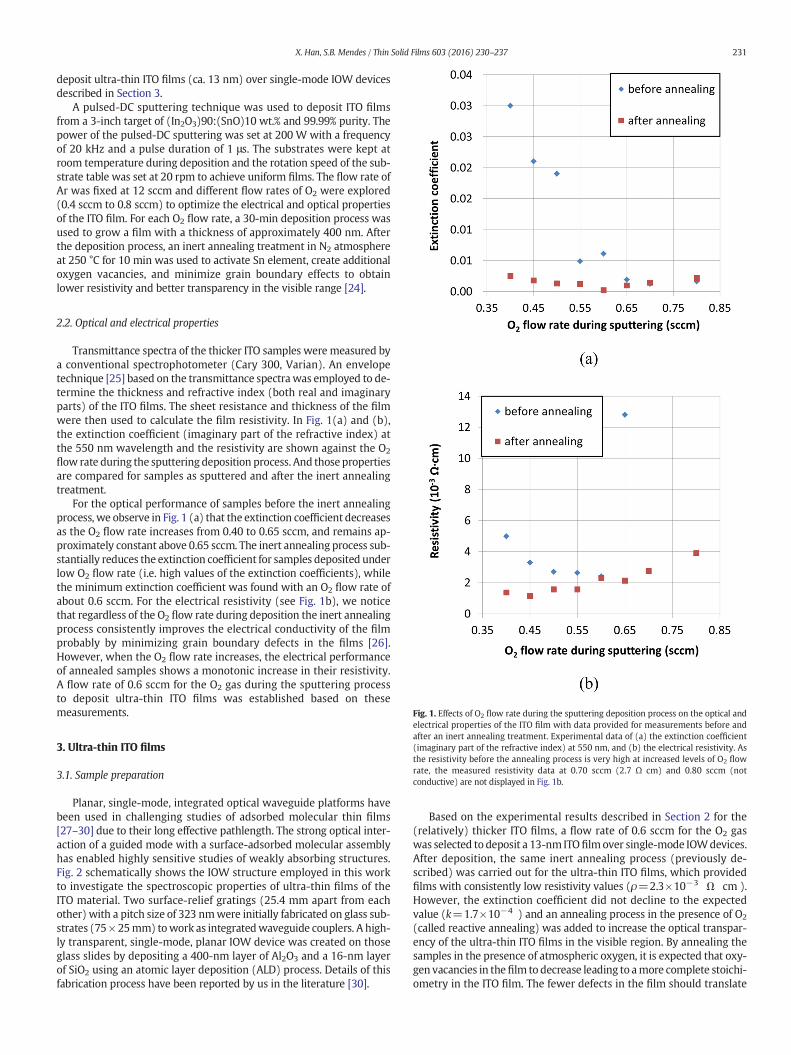
Fig. 1. Effects of O2 flow rate during the sputtering deposition process on the optical andelectrical properties of the ITO film with data provided for measurements before andafter an inert annealing treatment. Experimental data of (a) the extinction coefficient(imaginary part of the refractive index) at 550 nm, and (b) the electrical resistivity. Asthe resistivity before the annealing process is very high at increased levels of O2 flowrate, the measured resistivity data at 0.70 sccm (2.7 Ω cm) and 0.80 sccm (notconductive) are not displayed in Fig. 1b.
231X. Han, S.B. Mendes / Thin Solid Films 603 (2016) 230–237
deposit ultra-thin ITO films (ca. 13 nm) over single-mode IOW devicesdescribed in Section 3.
A pulsed-DC sputtering technique was used to deposit ITO filmsfrom a 3-inch target of (In2O3)90:(SnO)10 wt.% and 99.99% purity. Thepower of the pulsed-DC sputtering was set at 200 W with a frequencyof 20 kHz and a pulse duration of 1 μs. The substrates were kept atroom temperature during deposition and the rotation speed of the sub-strate table was set at 20 rpm to achieve uniform films. The flow rate ofAr was fixed at 12 sccm and different flow rates of O2 were explored(0.4 sccm to 0.8 sccm) to optimize the electrical and optical propertiesof the ITO film. For each O2 flow rate, a 30-min deposition process wasused to grow a film with a thickness of approximately 400 nm. Afterthe deposition process, an inert annealing treatment in N2 atmosphereat 250 °C for 10 min was used to activate Sn element, create additionaloxygen vacancies, and minimize grain boundary effects to obtainlower resistivity and better transparency in the visible range [24].
2.2. Optical and electrical properties
Transmittance spectra of the thicker ITO samples were measured bya conventional spectrophotometer (Cary 300, Varian). An envelopetechnique [25] based on the transmittance spectra was employed to de-termine the thickness and refractive index (both real and imaginaryparts) of the ITO films. The sheet resistance and thickness of the filmwere then used to calculate the film resistivity. In Fig. 1(a) and (b),the extinction coefficient (imaginary part of the refractive index) atthe 550 nm wavelength and the resistivity are shown against the O2
flow rate during the sputtering deposition process. And those propertiesare compared for samples as sputtered and after the inert annealingtreatment.
For the optical performance of samples before the inert annealingprocess, we observe in Fig. 1 (a) that the extinction coefficient decreasesas the O2 flow rate increases from 0.40 to 0.65 sccm, and remains ap-proximately constant above 0.65 sccm. The inert annealing process sub-stantially reduces the extinction coefficient for samples deposited underlow O2 flow rate (i.e. high values of the extinction coefficients), whilethe minimum extinction coefficient was found with an O2 flow rate ofabout 0.6 sccm. For the electrical resistivity (see Fig. 1b), we noticethat regardless of the O2 flow rate during deposition the inert annealingprocess consistently improves the electrical conductivity of the filmprobably by minimizing grain boundary defects in the films [26].However, when the O2 flow rate increases, the electrical performanceof annealed samples shows a monotonic increase in their resistivity.A flow rate of 0.6 sccm for the O2 gas during the sputtering processto deposit ultra-thin ITO films was established based on thesemeasurements.
3. Ultra-thin ITO films
3.1. Sample preparation
Planar, single-mode, integrated optical waveguide platforms havebeen used in challenging studies of adsorbed molecular thin films[27–30] due to their long effective pathlength. The strong optical inter-action of a guided mode with a surface-adsorbed molecular assemblyhas enabled highly sensitive studies of weakly absorbing structures.Fig. 2 schematically shows the IOW structure employed in this workto investigate the spectroscopic properties of ultra-thin films of theITO material. Two surface-relief gratings (25.4 mm apart from eachother) with a pitch size of 323 nmwere initially fabricated on glass sub-strates (75× 25mm) towork as integratedwaveguide couplers. A high-ly transparent, single-mode, planar IOW device was created on thoseglass slides by depositing a 400-nm layer of Al2O3 and a 16-nm layerof SiO2 using an atomic layer deposition (ALD) process. Details of thisfabrication process have been reported by us in the literature [30].
Based on the experimental results described in Section 2 for the(relatively) thicker ITO films, a flow rate of 0.6 sccm for the O2 gaswas selected to deposit a 13-nm ITOfilm over single-mode IOWdevices.After deposition, the same inert annealing process (previously de-scribed) was carried out for the ultra-thin ITO films, which providedfilms with consistently low resistivity values (ρ=2.3×10⁻³ Ω cm ).However, the extinction coefficient did not decline to the expectedvalue (k=1.7×10⁻⁴ ) and an annealing process in the presence of O2
(called reactive annealing) was added to increase the optical transpar-ency of the ultra-thin ITO films in the visible region. By annealing thesamples in the presence of atmospheric oxygen, it is expected that oxy-gen vacancies in thefilm to decrease leading to amore complete stoichi-ometry in the ITO film. The fewer defects in the film should translate

Fig. 2. Schematic structure of the single-mode integrated optical waveguide with an over-layer of an ultra-thin ITO film under investigation. An actual IOW device with broadbandlight dispersion of the out-coupled guided optical beam is shown in the inset.
Fig. 3. Power spectrum of the broadband out-coupled guided light at different values ofthe applied potential during a particular CV scan.
Fig. 4. Normalized transmittance for 3-folded cycles of CV scan obtained from broadbandspectrum of Fig. 3. Traces of the transmittance show a clear dependence on the appliedpotential, and that dependence changes for different wavelengths. For clarity, each curveis shifted by one division.
232 X. Han, S.B. Mendes / Thin Solid Films 603 (2016) 230–237
into lower residual absorption, and thus lower propagation losses forthe waveguide modes. We started the reactive annealing process at150 °C and,when the optical performancewas still insufficient, the tem-perature was raised by increments of 50 °C. A sample was heated untilan acceptable optical loss for the IOW device overcoated with anultra-thin ITO film was achieved. With this reactive annealing process,a total propagation loss of as low as 6 dB/cm was reached for thewhole waveguide stack, which includes the Al2O3 and SiO2 films andthe ultra-thin ITO film. The sheet resistance was about 2 kΩ/, whichconsistently corresponds to a value of 2.6×10⁻³ Ω cm for the resistiv-ity of the ITO film.
3.2. Spectroelectrochemical flowcell
Samples with low optical losses were placed in a buffer solution(Na2PO4, 5 mM, pH 7) for at least 24 h to chemically stabilize the ITOfilm. Then each sample was rinsed with DI water, dried by N2 gas, andset for electrical connections. A piece of carbon tape was used to attacha platinum wire onto the ITO film for electrical connection to thepotentiostat (CHI 600D). A layer of silver paste was placed around thetwo gratings to provide a uniform electric potential for the whole ITOfilm. After the silver paste became dry, an insulating epoxy layer wasplaced over it to prevent any chemical reaction between the silverpaste and the working electrolyte solution. After the epoxy layer wascured, the insulation between the epoxy layer and the platinum wirewas tested, as well as the conduction between the platinum wire andthe ITO film, which serves as the working electrode in our experiments.A homemade pseudo-reference electrode of Ag/AgCl and a platinumcounter electrode were inserted through the flow cell cover. The threeelectrodes were then connected to the potentiostat. The homemadepseudo-reference electrode in our electrolyte solution had a fairly con-stant potential offset of 85 mV compared to a standard Ag/AgCl refer-ence electrode in 1 M KCl solution (CHI). The potential valuesreported in this work are referenced to our pseudo Ag/AgCl referenceelectrode.
3.3. Cyclic voltammetry technique
At the first usage in the electrochemical cell, the ultra-thin ITO filmwas further stabilized by performing a few scans of cyclic voltammetry(CV) from −0.4 V to +0.8 V with various scan speed (0.02 V/s, 0.1 V/sand 0.2 V/s) until the current signal became stable.
A tungsten–halogen lamp was employed as a broadband lightsource. The TE polarization was selected by placing a sheet polarizer inthe optical path of the incoming beambefore arriving at the grating cou-pler. Additional details of the optical coupling configuration can befound in elsewhere [31]. The out-coupled optical signal was collectedby an optical fiber and delivered to a spectrometer that was connectedto an intensified CCD (ICCD, Princeton, PI-MAX 3). The out-coupled op-tical signal under CV potential modulation from −0.4 V to +0.8 V at a
scan-speed of 0.02 V/s was collected. The ICCDwas set to an acquisitionfrequency of 2 Hz with having an exposure time of 200 ms for eachframe.
On completion of these measurements, a trace corresponding to adark signal was collected by injecting black ink into the cell andperforming an acquisition under the same exposure time. Fig. 3 showsthe out-coupled broadband power spectrum at different values of theelectric potential during a particular CV scan.
From the measurements above we calculated the normalized trans-mittance, tN, according to Eq. (1) for a particular wavelength:
tN λð Þ ¼ IV−I min
I max−I minð1Þ
where IV is the out-coupled intensity (ICCD counts) at the electric po-tential V, and Imin and Imax are respectively theminimum andmaximumout-coupled intensities at a particular wavelength when the potentialwas scanned from +0.8 V to −0.4 V over a few cycles. The traces oftN for a set of discrete wavelengths from 510 nm to 600 nm are shownin Fig. 4. Each wavelength is vertically-shifted by one unit for clarity,and the several cycles of the CV scans are folded into one segment. Fora particular wavelength, we observe that the folded traces demonstratevery good repeatability and consistency for the results during the CV
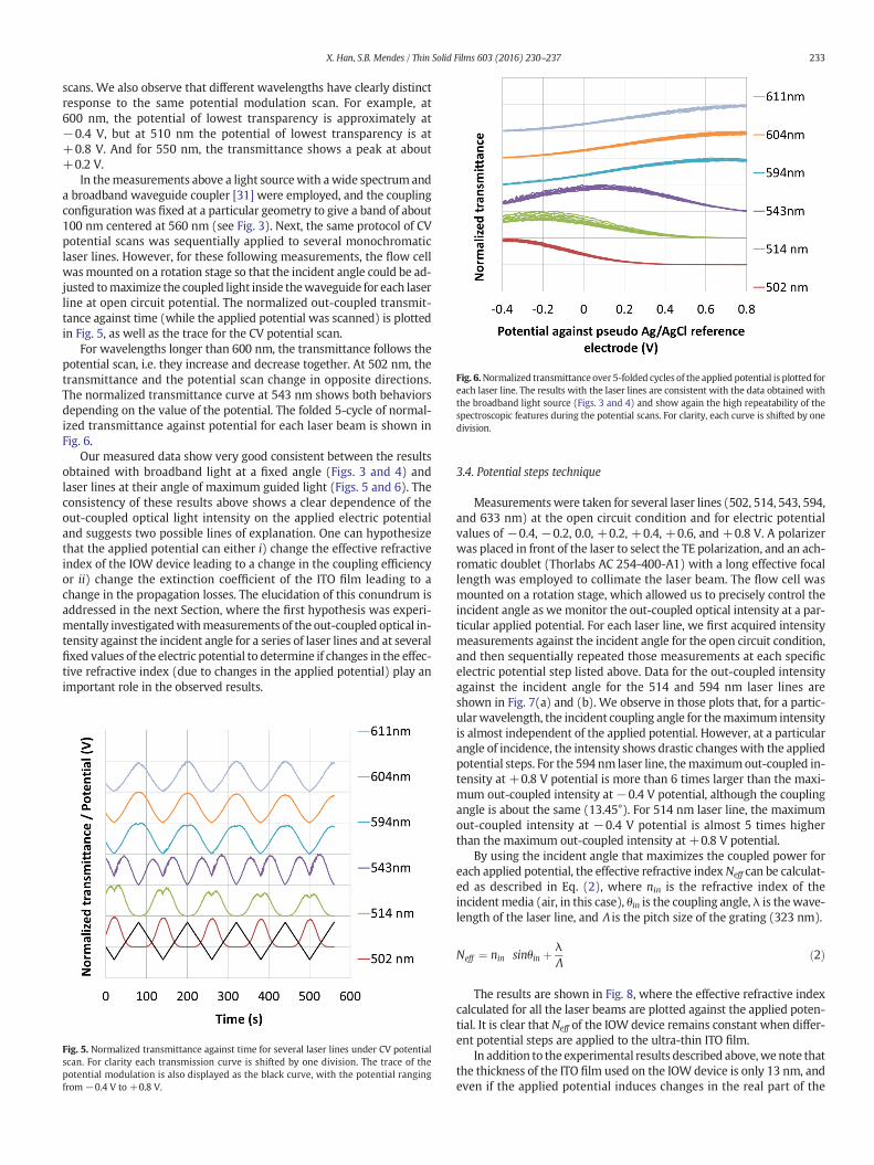
Fig. 6.Normalized transmittance over 5-folded cycles of the applied potential is plotted foreach laser line. The results with the laser lines are consistent with the data obtained withthe broadband light source (Figs. 3 and 4) and show again the high repeatability of thespectroscopic features during the potential scans. For clarity, each curve is shifted by onedivision.
233X. Han, S.B. Mendes / Thin Solid Films 603 (2016) 230–237
scans. We also observe that different wavelengths have clearly distinctresponse to the same potential modulation scan. For example, at600 nm, the potential of lowest transparency is approximately at−0.4 V, but at 510 nm the potential of lowest transparency is at+0.8 V. And for 550 nm, the transmittance shows a peak at about+0.2 V.
In themeasurements above a light sourcewith awide spectrum anda broadband waveguide coupler [31] were employed, and the couplingconfiguration was fixed at a particular geometry to give a band of about100 nm centered at 560 nm (see Fig. 3). Next, the same protocol of CVpotential scans was sequentially applied to several monochromaticlaser lines. However, for these following measurements, the flow cellwasmounted on a rotation stage so that the incident angle could be ad-justed tomaximize the coupled light inside thewaveguide for each laserline at open circuit potential. The normalized out-coupled transmit-tance against time (while the applied potential was scanned) is plottedin Fig. 5, as well as the trace for the CV potential scan.
For wavelengths longer than 600 nm, the transmittance follows thepotential scan, i.e. they increase and decrease together. At 502 nm, thetransmittance and the potential scan change in opposite directions.The normalized transmittance curve at 543 nm shows both behaviorsdepending on the value of the potential. The folded 5-cycle of normal-ized transmittance against potential for each laser beam is shown inFig. 6.
Our measured data show very good consistent between the resultsobtained with broadband light at a fixed angle (Figs. 3 and 4) andlaser lines at their angle of maximum guided light (Figs. 5 and 6). Theconsistency of these results above shows a clear dependence of theout-coupled optical light intensity on the applied electric potentialand suggests two possible lines of explanation. One can hypothesizethat the applied potential can either i) change the effective refractiveindex of the IOW device leading to a change in the coupling efficiencyor ii) change the extinction coefficient of the ITO film leading to achange in the propagation losses. The elucidation of this conundrum isaddressed in the next Section, where the first hypothesis was experi-mentally investigatedwithmeasurements of the out-coupled optical in-tensity against the incident angle for a series of laser lines and at severalfixed values of the electric potential to determine if changes in the effec-tive refractive index (due to changes in the applied potential) play animportant role in the observed results.
Fig. 5. Normalized transmittance against time for several laser lines under CV potentialscan. For clarity each transmission curve is shifted by one division. The trace of thepotential modulation is also displayed as the black curve, with the potential rangingfrom −0.4 V to +0.8 V.
3.4. Potential steps technique
Measurementswere taken for several laser lines (502, 514, 543, 594,and 633 nm) at the open circuit condition and for electric potentialvalues of −0.4, −0.2, 0.0, +0.2, +0.4, +0.6, and +0.8 V. A polarizerwas placed in front of the laser to select the TE polarization, and an ach-romatic doublet (Thorlabs AC 254-400-A1) with a long effective focallength was employed to collimate the laser beam. The flow cell wasmounted on a rotation stage, which allowed us to precisely control theincident angle as we monitor the out-coupled optical intensity at a par-ticular applied potential. For each laser line, we first acquired intensitymeasurements against the incident angle for the open circuit condition,and then sequentially repeated those measurements at each specificelectric potential step listed above. Data for the out-coupled intensityagainst the incident angle for the 514 and 594 nm laser lines areshown in Fig. 7(a) and (b). We observe in those plots that, for a partic-ularwavelength, the incident coupling angle for themaximum intensityis almost independent of the applied potential. However, at a particularangle of incidence, the intensity shows drastic changes with the appliedpotential steps. For the 594 nm laser line, themaximumout-coupled in-tensity at +0.8 V potential is more than 6 times larger than the maxi-mum out-coupled intensity at −0.4 V potential, although the couplingangle is about the same (13.45°). For 514 nm laser line, the maximumout-coupled intensity at −0.4 V potential is almost 5 times higherthan the maximum out-coupled intensity at +0.8 V potential.
By using the incident angle that maximizes the coupled power foreach applied potential, the effective refractive indexNeff can be calculat-ed as described in Eq. (2), where nin is the refractive index of theincidentmedia (air, in this case), θin is the coupling angle, λ is thewave-length of the laser line, and Λ is the pitch size of the grating (323 nm).
Neff ¼ nin sinθin þλΛ
ð2Þ
The results are shown in Fig. 8, where the effective refractive indexcalculated for all the laser beams are plotted against the applied poten-tial. It is clear that Neff of the IOW device remains constant when differ-ent potential steps are applied to the ultra-thin ITO film.
In addition to the experimental results described above,we note thatthe thickness of the ITO film used on the IOW device is only 13 nm, andeven if the applied potential induces changes in the real part of the
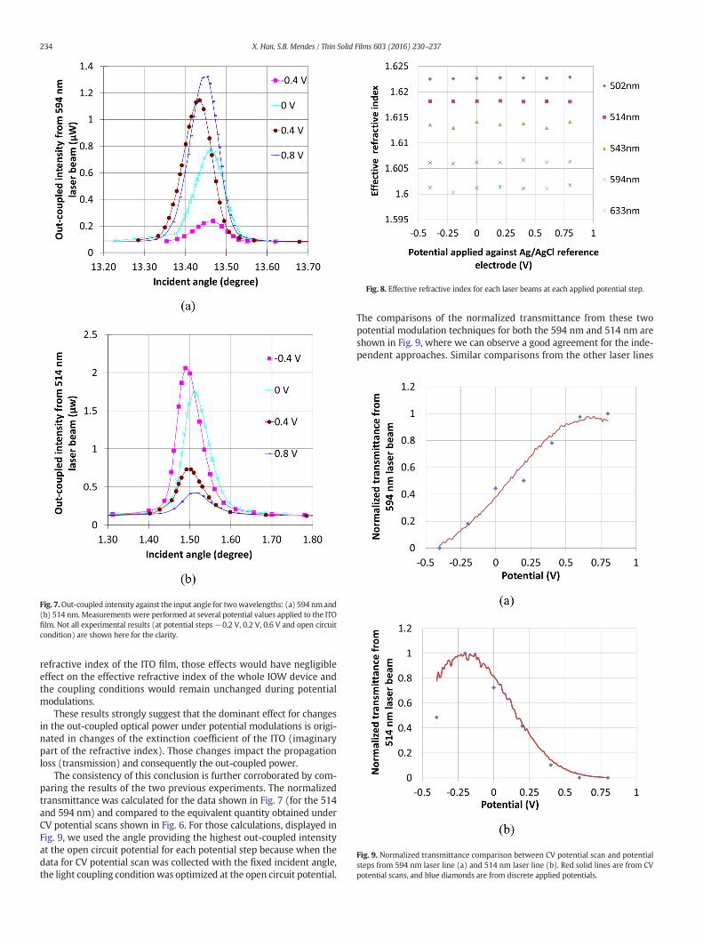
Fig. 7.Out-coupled intensity against the input angle for twowavelengths: (a) 594 nmand(b) 514 nm. Measurements were performed at several potential values applied to the ITOfilm. Not all experimental results (at potential steps−0.2 V, 0.2 V, 0.6 V and open circuitcondition) are shown here for the clarity.
Fig. 8. Effective refractive index for each laser beams at each applied potential step.
Fig. 9. Normalized transmittance comparison between CV potential scan and potentialsteps from 594 nm laser line (a) and 514 nm laser line (b). Red solid lines are from CVpotential scans, and blue diamonds are from discrete applied potentials.
234 X. Han, S.B. Mendes / Thin Solid Films 603 (2016) 230–237
refractive index of the ITO film, those effects would have negligibleeffect on the effective refractive index of the whole IOW device andthe coupling conditions would remain unchanged during potentialmodulations.
These results strongly suggest that the dominant effect for changesin the out-coupled optical power under potential modulations is origi-nated in changes of the extinction coefficient of the ITO (imaginarypart of the refractive index). Those changes impact the propagationloss (transmission) and consequently the out-coupled power.
The consistency of this conclusion is further corroborated by com-paring the results of the two previous experiments. The normalizedtransmittance was calculated for the data shown in Fig. 7 (for the 514and 594 nm) and compared to the equivalent quantity obtained underCV potential scans shown in Fig. 6. For those calculations, displayed inFig. 9, we used the angle providing the highest out-coupled intensityat the open circuit potential for each potential step because when thedata for CV potential scan was collected with the fixed incident angle,the light coupling conditionwas optimized at the open circuit potential.
The comparisons of the normalized transmittance from these twopotential modulation techniques for both the 594 nm and 514 nm areshown in Fig. 9, where we can observe a good agreement for the inde-pendent approaches. Similar comparisons from the other laser lines
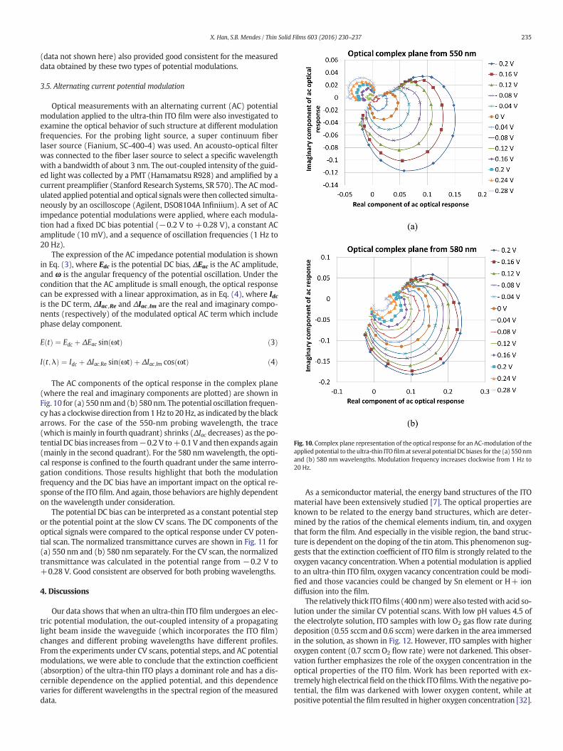
Fig. 10. Complex plane representation of the optical response for an AC-modulation of theapplied potential to theultra-thin ITOfilm at several potential DCbiases for the (a) 550nmand (b) 580 nm wavelengths. Modulation frequency increases clockwise from 1 Hz to20 Hz.
235X. Han, S.B. Mendes / Thin Solid Films 603 (2016) 230–237
(data not shown here) also provided good consistent for the measureddata obtained by these two types of potential modulations.
3.5. Alternating current potential modulation
Optical measurements with an alternating current (AC) potentialmodulation applied to the ultra-thin ITO film were also investigated toexamine the optical behavior of such structure at different modulationfrequencies. For the probing light source, a super continuum fiberlaser source (Fianium, SC-400-4) was used. An acousto-optical filterwas connected to the fiber laser source to select a specific wavelengthwith a bandwidth of about 3 nm. The out-coupled intensity of the guid-ed light was collected by a PMT (Hamamatsu R928) and amplified by acurrent preamplifier (Stanford Research Systems, SR 570). The ACmod-ulated applied potential and optical signalswere then collected simulta-neously by an oscilloscope (Agilent, DSO8104A Infiniium). A set of ACimpedance potential modulations were applied, where each modula-tion had a fixed DC bias potential (−0.2 V to +0.28 V), a constant ACamplitude (10 mV), and a sequence of oscillation frequencies (1 Hz to20 Hz).
The expression of the AC impedance potential modulation is shownin Eq. (3), where Edc is the potential DC bias, ΔEac is the AC amplitude,and ω is the angular frequency of the potential oscillation. Under thecondition that the AC amplitude is small enough, the optical responsecan be expressed with a linear approximation, as in Eq. (4), where Idcis the DC term, ΔIac ,Re and ΔIac , Im are the real and imaginary compo-nents (respectively) of the modulated optical AC term which includephase delay component.
E tð Þ ¼ Edc þ ΔEac sin ωtð Þ ð3Þ
I t;λð Þ ¼ Idc þ ΔIac;Re sin ωtð Þ þ ΔIac;Im cos ωtð Þ ð4Þ
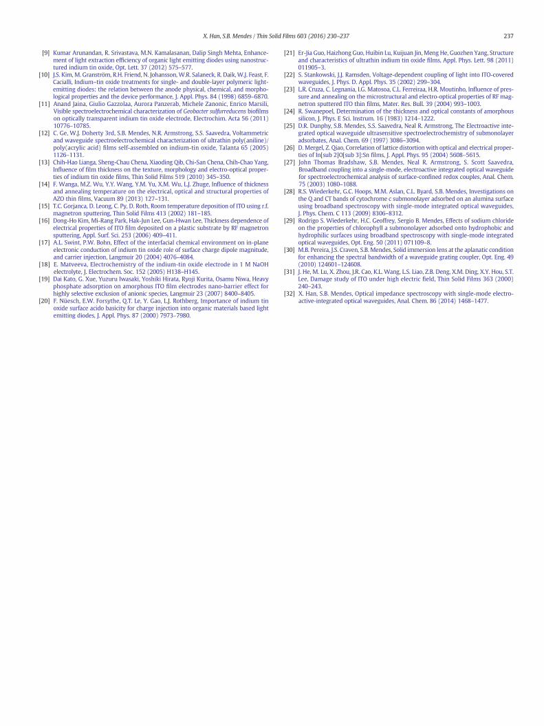
The AC components of the optical response in the complex plane(where the real and imaginary components are plotted) are shown inFig. 10 for (a) 550 nmand (b) 580 nm. The potential oscillation frequen-cy has a clockwise direction from1Hz to 20Hz, as indicated by the blackarrows. For the case of the 550-nm probing wavelength, the trace(which is mainly in fourth quadrant) shrinks (ΔIac decreases) as the po-tential DC bias increases from−0.2 V to+0.1 V and then expands again(mainly in the second quadrant). For the 580 nmwavelength, the opti-cal response is confined to the fourth quadrant under the same interro-gation conditions. Those results highlight that both the modulationfrequency and the DC bias have an important impact on the optical re-sponse of the ITO film. And again, those behaviors are highly dependenton the wavelength under consideration.
The potential DC bias can be interpreted as a constant potential stepor the potential point at the slow CV scans. The DC components of theoptical signals were compared to the optical response under CV poten-tial scan. The normalized transmittance curves are shown in Fig. 11 for(a) 550 nm and (b) 580 nm separately. For the CV scan, the normalizedtransmittance was calculated in the potential range from −0.2 V to+0.28 V. Good consistent are observed for both probing wavelengths.
4. Discussions
Our data shows that when an ultra-thin ITO film undergoes an elec-tric potential modulation, the out-coupled intensity of a propagatinglight beam inside the waveguide (which incorporates the ITO film)changes and different probing wavelengths have different profiles.From the experiments under CV scans, potential steps, and AC potentialmodulations, we were able to conclude that the extinction coefficient(absorption) of the ultra-thin ITO plays a dominant role and has a dis-cernible dependence on the applied potential, and this dependencevaries for different wavelengths in the spectral region of the measureddata.
As a semiconductor material, the energy band structures of the ITOmaterial have been extensively studied [7]. The optical properties areknown to be related to the energy band structures, which are deter-mined by the ratios of the chemical elements indium, tin, and oxygenthat form the film. And especially in the visible region, the band struc-ture is dependent on the doping of the tin atom. This phenomenon sug-gests that the extinction coefficient of ITO film is strongly related to theoxygen vacancy concentration. When a potential modulation is appliedto an ultra-thin ITO film, oxygen vacancy concentration could be modi-fied and those vacancies could be changed by Sn element or H+ iondiffusion into the film.
The relatively thick ITOfilms (400nm)were also testedwith acid so-lution under the similar CV potential scans. With low pH values 4.5 ofthe electrolyte solution, ITO samples with low O2 gas flow rate duringdeposition (0.55 sccm and 0.6 sccm) were darken in the area immersedin the solution, as shown in Fig. 12. However, ITO samples with higheroxygen content (0.7 sccm O2 flow rate) were not darkened. This obser-vation further emphasizes the role of the oxygen concentration in theoptical properties of the ITO film. Work has been reported with ex-tremely high electricalfield on the thick ITOfilms.With the negative po-tential, the film was darkened with lower oxygen content, while atpositive potential the film resulted in higher oxygen concentration [32].
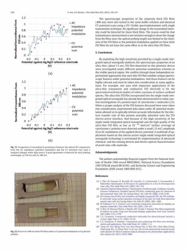
Fig. 12. Picture of a 400 nm thick ITO films under a CV potential modulation in 4.5 pH acidsolution.
Fig. 11. Comparison of normalized transmittance between the optical DC componentsfrom the AC impedance potential modulation and the CV potential scan used atungsten-halogen white light source. A good agreement is observed for each probingwavelength (a) 550 nm and (b) 580 nm.
236 X. Han, S.B. Mendes / Thin Solid Films 603 (2016) 230–237
The spectroscopic properties of the relatively thick ITO films(400 nm) were also tested in the same buffer solution and identicalCV potential scans using a UV–Visible spectrophotometer with singletransmission technique. No significant change in the transmitted inten-sity could be detected for these thick films. The reason could be thattransmittancemeasurement is not sensitive enough to show the changefrom the films since the optical probing length was limited to the thick-ness of the ITO films or the potential modulation applied on these thickITO films do not have the same effect as in the ultra-thin ITO films.
5. Conclusions
By exploiting the high sensitivity provided by a single-mode inte-grated optical waveguide platform, the spectroscopic properties of anultra-thin (about 13 nm) ITO film deposited on this photonic devicewere investigated under different potential modulation schemes inthe visible spectral region. We confirm through those independent ex-perimental approaches that such thin ITO film exhibits unique spectro-scopic features under potential modulations. And those features can behighly relevant and must be taken into consideration in many applica-tions. For example, one area with important applications of theultra-thin transparent and conductive ITO electrode is for thespectroelectrochemical studies of redox reactions of surface-confinedspecies. The ultra-thin ITO film incorporated into the single-mode inte-grated optical waveguide has already been demonstrated in redox reac-tion investigations of a protein layer of cytochrome-c molecules [23].When a proper analysis of the ITO features discussed here were takeninto consideration, experimental data taken under AC potential modu-lation allowed us to optically retrieve accurate information for the elec-tron transfer rate of this protein assembly adsorbed onto the ITOelectro-active interface. And because of the high sensitivity of thesingle-mode integrated optical waveguide and the high quality of theultra-thin ITO film, as low as 10−14 mol/cm2 surface coverage ofcytochrome-c proteinswere detected under a small (15mV) amplitudeof an ACmodulation of the applied electric potential. A multitude of ap-plications based on this electro-active single-mode integrated opticalwaveguide technology is envisioned for implementation of advancedchemical- and bio-sensing devices and electro-optical characterizationof novel solar cells materials.
Acknowledgments
The authors acknowledge financial support from the National Insti-tute of Health (NIH award RR022864), National Science Foundation(NSF EPSCoR award 0814194), and Kentucky Science and EngineeringFoundation (KSEF award 1869-RDE-012).
References
[1] J. Pláa, M. Tamasia, R. Rizzolib, M. Losurdoc, E. Centurionib, C. Summonteb, F.Rubinellid, Optimization of ITO layers for applications in a-Si/c-Si heterojunctionsolar cells, Thin Solid Films 425 (2003) 185–192.
[2] Supachai Ngamsinlapasathiana, Thammanoon Sreethawongb, Yoshikazu Suzukia,Susumu Yoshikawaa, Doubled layered ITO/SnO2 conducting glass for substrate ofdye-sensitized solar cells, Sol. Energy Mater. Sol. Cells 90 (2006) 2129–2140.
[3] Jin-A Jeong, Han-Ki Kim, Low resistance and highly transparent ITO–Ag–ITOmultilay-er electrode using surface plasmon resonance of Ag layer for bulk-heterojunctionorganic solar cells, Sol. Energy Mater. Sol. Cells 93 (2009) 1801–1809.
[4] M. Fahland, P. K., C. Charton, Low resisitivity transparent electrodes for displays onpolymer substrates, Thin Solid Films 392 (2001) 334–337.
[5] U. Betz, M. Kharrazi Olsson, J. Marthy, M.F. Escolá, F. Atamny, Thin films engineeringof indium tin oxide: large area flat panel displays application, Surf. Coat. Technol.200 (2006) 5751–5759.
[6] C.G. Granqvist, Transparent conductive electrodes for electrochromic devices areview, Appl. Phys. A 57 (1993) 19–24.
[7] C.G. Granqvist, A. Hultaker, Transparent and conducting ITO films new develop-ments and applications, Thin Solid Films 411 (2002) 1–5.
[8] Yung-Chi Yao, Meng-Tsan Tsai, Hsu-Cheng Hsu, Li-Wei She, Chun-Mao Cheng,Chien-Jang Wu, Yi-Ching Chen, Ya-Ju Lee, Use of two-dimensional nanorod arrayswith slanted ITO film to enhance optical absorption for photovoltaic applications,Opt. Express 20 (2012) 3479–3489.
237X. Han, S.B. Mendes / Thin Solid Films 603 (2016) 230–237
[9] Kumar Arunandan, R. Srivastava, M.N. Kamalasanan, Dalip Singh Mehta, Enhance-ment of light extraction efficiency of organic light emitting diodes using nanostruc-tured indium tin oxide, Opt. Lett. 37 (2012) 575–577.
[10] J.S. Kim, M. Granström, R.H. Friend, N. Johansson,W.R. Salaneck, R. Daik,W.J. Feast, F.Cacialli, Indium–tin oxide treatments for single- and double-layer polymeric light-emitting diodes: the relation between the anode physical, chemical, and morpho-logical properties and the device performance, J. Appl. Phys. 84 (1998) 6859–6870.
[11] Anand Jaina, Giulio Gazzolaa, Aurora Panzerab, Michele Zanonic, Enrico Marsili,Visible spectroelectrochemical characterization of Geobacter sulfurreducens biofilmson optically transparent indium tin oxide electrode, Electrochim. Acta 56 (2011)10776–10785.
[12] C. Ge, W.J. Doherty 3rd, S.B. Mendes, N.R. Armstrong, S.S. Saavedra, Voltammetricand waveguide spectroelectrochemical characterization of ultrathin poly(aniline)/poly(acrylic acid) films self-assembled on indium-tin oxide, Talanta 65 (2005)1126–1131.
[13] Chih-Hao Lianga, Sheng-Chau Chena, Xiaoding Qib, Chi-San Chena, Chih-Chao Yang,Influence of film thickness on the texture, morphology and electro-optical proper-ties of indium tin oxide films, Thin Solid Films 519 (2010) 345–350.
[14] F. Wanga, M.Z. Wu, Y.Y. Wang, Y.M. Yu, X.M. Wu, L.J. Zhuge, Influence of thicknessand annealing temperature on the electrical, optical and structural properties ofAZO thin films, Vacuum 89 (2013) 127–131.
[15] T.C. Gorjanca, D. Leong, C. Py, D. Roth, Room temperature deposition of ITO using r.f.magnetron sputtering, Thin Solid Films 413 (2002) 181–185.
[16] Dong-Ho Kim, Mi-Rang Park, Hak-Jun Lee, Gun-Hwan Lee, Thickness dependence ofelectrical properties of ITO film deposited on a plastic substrate by RF magnetronsputtering, Appl. Surf. Sci. 253 (2006) 409–411.
[17] A.L. Swint, P.W. Bohn, Effect of the interfacial chemical environment on in-planeelectronic conduction of indium tin oxide role of surface charge dipole magnitude,and carrier injection, Langmuir 20 (2004) 4076–4084.
[18] E. Matveeva, Electrochemistry of the indium-tin oxide electrode in 1 M NaOHelectrolyte, J. Electrochem. Soc. 152 (2005) H138–H145.
[19] Dai Kato, G. Xue, Yuzuru Iwasaki, Yoshiki Hirata, Ryoji Kurita, Osamu Niwa, Heavyphosphate adsorption on amorphous ITO film electrodes nano-barrier effect forhighly selective exclusion of anionic species, Langmuir 23 (2007) 8400–8405.
[20] F. Nüesch, E.W. Forsythe, Q.T. Le, Y. Gao, L.J. Rothberg, Importance of indium tinoxide surface acido basicity for charge injection into organic materials based lightemitting diodes, J. Appl. Phys. 87 (2000) 7973–7980.
[21] Er-Jia Guo, Haizhong Guo, Huibin Lu, Kuijuan Jin, Meng He, Guozhen Yang, Structureand characteristics of ultrathin indium tin oxide films, Appl. Phys. Lett. 98 (2011)011905–3.
[22] S. Stankowski, J.J. Ramsden, Voltage-dependent coupling of light into ITO-coveredwaveguides, J. Phys. D. Appl. Phys. 35 (2002) 299–304.
[23] L.R. Cruza, C. Legnania, I.G. Matosoa, C.L. Ferreiraa, H.R. Moutinho, Influence of pres-sure and annealing on the microstructural and electro-optical properties of RF mag-netron sputtered ITO thin films, Mater. Res. Bull. 39 (2004) 993–1003.
[24] R. Swanepoel, Determination of the thickness and optical constants of amorphoussilicon, J. Phys. E Sci. Instrum. 16 (1983) 1214–1222.
[25] D.R. Dunphy, S.B. Mendes, S.S. Saavedra, Neal R. Armstrong, The Electroactive inte-grated optical waveguide ultrasensitive spectroelectrochemistry of submonolayeradsorbates, Anal. Chem. 69 (1997) 3086–3094.
[26] D. Mergel, Z. Qiao, Correlation of lattice distortion with optical and electrical proper-ties of In[sub 2]O[sub 3]:Sn films, J. Appl. Phys. 95 (2004) 5608–5615.
[27] John Thomas Bradshaw, S.B. Mendes, Neal R. Armstrong, S. Scott Saavedra,Broadband coupling into a single-mode, electroactive integrated optical waveguidefor spectroelectrochemical analysis of surface-confined redox couples, Anal. Chem.75 (2003) 1080–1088.
[28] R.S. Wiederkehr, G.C. Hoops, M.M. Aslan, C.L. Byard, S.B. Mendes, Investigations onthe Q and CT bands of cytochrome c submonolayer adsorbed on an alumina surfaceusing broadband spectroscopy with single-mode integrated optical waveguides,J. Phys. Chem. C 113 (2009) 8306–8312.
[29] Rodrigo S. Wiederkehr, H.C. Geoffrey, Sergio B. Mendes, Effects of sodium chlorideon the properties of chlorophyll a submonolayer adsorbed onto hydrophobic andhydrophilic surfaces using broadband spectroscopy with single-mode integratedoptical waveguides, Opt. Eng. 50 (2011) 071109–8.
[30] M.B. Pereira, J.S. Craven, S.B. Mendes, Solid immersion lens at the aplanatic conditionfor enhancing the spectral bandwidth of a waveguide grating coupler, Opt. Eng. 49(2010) 124601–124608.
[31] J. He, M. Lu, X. Zhou, J.R. Cao, K.L. Wang, L.S. Liao, Z.B. Deng, X.M. Ding, X.Y. Hou, S.T.Lee, Damage study of ITO under high electric field, Thin Solid Films 363 (2000)240–243.
[32] X. Han, S.B. Mendes, Optical impedance spectroscopy with single-mode electro-active-integrated optical waveguides, Anal. Chem. 86 (2014) 1468–1477.