Thin-Film Solid-State Electroluminescent Devices Based On...
18
Thin-Film Solid-State Electroluminescent Devices Based On Tris(2,2′-bipyridine)ruthenium(II) Complexes Mihai Buda, Gregory Kalyuzhny, and Allen J. Bard* Contribution from the Department of Chemistry and Biochemistry and Center for Nano- and Molecular Science and Technology, The UniVersity of Texas at Austin, Austin, Texas 78712 Received December 20, 2001 Abstract: The behavior of light-emitting electrochemical cells (LEC) based on solid films (∼100 nm) of tris(2,2′-bipyridine)ruthenium(II) between an ITO anode and a Ga-In cathode was investigated. The response times were strongly influenced by the nature of the counterion: small anions (BF4 - and ClO4 - ) led to relatively fast transients, while large anions (PF6 - , AsF6 - ) produced a slow time-response. From comparative experiments of cells prepared and tested in a glovebox to those in ambient, mobility of the anions in these films appears to be related to the presence of traces of water from atmospheric moisture. An electrochemical model is proposed to describe the behavior of these LECs. The simulation results agreed well with experimental transients of current and light emission as a function of time and show that the charge injection is asymmetric at the two electrodes. At a small bias, electrons are the major carriers, while for a larger bias the conduction becomes bipolar. Introduction Organic light-emitting devices based on tris(2,2′-bipyridine)- ruthenium(II) complexes are promising candidates for high- efficiency, low-voltage devices. Although there is vast literature dealing with organic light-emitting diodes based on polymers and Alq 3 , solid-state electroluminescent devices based on inorganic salts such as Ru(bpy) 3 2+ as the active substrate have only recently been investigated in detail 1,2 (although the first paper describing a light-emitting device based on a ruthenium phenanthroline complex was published in 1996 3 ). Basically, a thin film (∼100 nm) of Ru(bpy) 3 X 2 (where X is an anion like ClO 4 - or BF 4 - ) is deposited by spin coating on an indium tin oxide (ITO) substrate, and a metal contact is formed on the top. Over the past years, organic light-emitting devices that incorporate mobile ions have been referred to as organic light- emitting electrochemical cells (LECs), in contrast to OLEDs that behave more as solid-state semiconductor devices. 4,5 OLEDs behave analogously to solid-state semiconductor devices. There are a negligible number of mobile ions in the film, and charge injection requires ohmic contacts at the electrodes. LECs involve films in which there are mobile ions, and charge injection is relatively independent of the nature of the contacts. In both cases, however, chemical reactions at the contacts can occur, and these can produce deleterious effects on the cell operation. There are several important features that distinguish LECs from conventional OLEDs: (1) The “turn-on” voltage of LECs is close to the optical gap and is only very weakly dependent on the film thickness. (2) The quantum efficiencies of LECs do not depend on the electrode work-function. (3) LECs exhibit symmetrical current-voltage and light-voltage characteristics. All of the above characteristics are observed for tris(2,2′- bipyridine)ruthenium salt light-emitting devices, suggesting that these devices are, in fact, LECs. In the present paper, we report the general behavior of these light-emitting devices and demonstrate that the response depends critically on the nature of the anion and whether the cell is prepared and tested in the ambient or in an inert atmosphere box. We propose an electrochemical model and show simulation results that correlate well with the observed behavior of these cells. Experimental Section Ru(bpy)3(ClO4)2 was prepared by a metathesis reaction between commercial Ru(bpy)3Cl2 (Aldrich) and excess sodium perchlorate. 6 The resulting crystals were recrystallized from acetonitrile/benzene and dried under vacuum at ∼100 °C for several hours. Ru(bpy)3(BF4)2, Ru(bpy)3- (PF6)2, and Ru(bpy)3(AsF6)2 were prepared using similar procedures with the appropriate sodium or ammonium salts. ITO covered glass (∼20 Ω/0, Delta Technologies) was thoroughly cleaned before device preparation by sonication for 20 min in a 20% (vol) solution of ethanolamine in highly pure Millipore water at ∼60 °C, followed by three rinsing/sonication steps with pure water at room temperature to remove traces of ethanolamine, and drying under vacuum for several hours at ∼80 °C. Ru(bpy)3(X)2 solutions in acetonitrile were always filtered through 0.2 μm syringe filters before use. Typically, the Ru(bpy)3(X)2 films (∼100 nm) were spin-coated (Headway Research) from a 4% (w/v) acetonitrile solution at 2000 rpm, onto clean ITO covered glass. After spin coating, the device was dried under vacuum for at least 8 h at * To whom correspondence should be addressed. E-mail: ajbard@ mail.utexas.edu. (1) Handy, E. S.; Pal, A. J.; Rubner, M. F. J. Am. Chem. Soc. 1999, 121, 3525. (2) Gao, F. G.; Bard, A. J. J. Am. Chem. Soc. 2000, 122, 7426. (3) Lee, J.-K.; Yoo, D. S.; Handy, E. S.; Rubner, M. F. Appl. Phys. Lett. 1996, 69, 1686. (4) Mitschke, U.; Ba ¨uerle, P. J. Mater. Chem. 2000, 10, 1471. (5) Pei, Q.; Yang, Y. Synth. Met. 1996, 80, 131. (6) McCord, P.; Bard, A. J. J. Electroanal. Chem. 1991, 318, 91. Published on Web 05/03/2002 6090 9 J. AM. CHEM. SOC. 2002, 124, 6090-6098 10.1021/ja017834h CCC: $22.00 © 2002 American Chemical Society
Transcript of Thin-Film Solid-State Electroluminescent Devices Based On...

Thin-Film Solid-State Electroluminescent Devices Based OnTris(2,2 ′-bipyridine)ruthenium(II) Complexes
Mihai Buda, Gregory Kalyuzhny, and Allen J. Bard*
Contribution from the Department of Chemistry and Biochemistry and Center for Nano- andMolecular Science and Technology, The UniVersity of Texas at Austin, Austin, Texas 78712
Received December 20, 2001
Abstract: The behavior of light-emitting electrochemical cells (LEC) based on solid films (∼100 nm) oftris(2,2′-bipyridine)ruthenium(II) between an ITO anode and a Ga-In cathode was investigated. Theresponse times were strongly influenced by the nature of the counterion: small anions (BF4
- and ClO4-)
led to relatively fast transients, while large anions (PF6-, AsF6
-) produced a slow time-response. Fromcomparative experiments of cells prepared and tested in a glovebox to those in ambient, mobility of theanions in these films appears to be related to the presence of traces of water from atmospheric moisture.An electrochemical model is proposed to describe the behavior of these LECs. The simulation resultsagreed well with experimental transients of current and light emission as a function of time and show thatthe charge injection is asymmetric at the two electrodes. At a small bias, electrons are the major carriers,while for a larger bias the conduction becomes bipolar.
Introduction
Organic light-emitting devices based on tris(2,2′-bipyridine)-ruthenium(II) complexes are promising candidates for high-efficiency, low-voltage devices. Although there is vast literaturedealing with organic light-emitting diodes based on polymersand Alq3, solid-state electroluminescent devices based oninorganic salts such as Ru(bpy)3
2+ as the active substrate haveonly recently been investigated in detail1,2 (although the firstpaper describing a light-emitting device based on a rutheniumphenanthroline complex was published in 19963). Basically, athin film (∼100 nm) of Ru(bpy)3X2 (where X is an anion likeClO4
- or BF4-) is deposited by spin coating on an indium tin
oxide (ITO) substrate, and a metal contact is formed on thetop. Over the past years, organic light-emitting devices thatincorporate mobile ions have been referred to as organic light-emitting electrochemical cells (LECs), in contrast to OLEDsthat behave more as solid-state semiconductor devices.4,5 OLEDsbehave analogously to solid-state semiconductor devices. Thereare a negligible number of mobile ions in the film, and chargeinjection requires ohmic contacts at the electrodes. LECs involvefilms in which there are mobile ions, and charge injection isrelatively independent of the nature of the contacts. In bothcases, however, chemical reactions at the contacts can occur,and these can produce deleterious effects on the cell operation.There are several important features that distinguish LECs fromconventional OLEDs: (1) The “turn-on” voltage of LECs is
close to the optical gap and is only very weakly dependent onthe film thickness. (2) The quantum efficiencies of LECs donot depend on the electrode work-function. (3) LECs exhibitsymmetrical current-voltage and light-voltage characteristics.
All of the above characteristics are observed for tris(2,2′-bipyridine)ruthenium salt light-emitting devices, suggesting thatthese devices are, in fact, LECs.
In the present paper, we report the general behavior of theselight-emitting devices and demonstrate that the response dependscritically on the nature of the anion and whether the cell isprepared and tested in the ambient or in an inert atmospherebox. We propose an electrochemical model and show simulationresults that correlate well with the observed behavior of thesecells.
Experimental Section
Ru(bpy)3(ClO4)2 was prepared by a metathesis reaction betweencommercial Ru(bpy)3Cl2 (Aldrich) and excess sodium perchlorate.6 Theresulting crystals were recrystallized from acetonitrile/benzene and driedunder vacuum at∼100°C for several hours. Ru(bpy)3(BF4)2, Ru(bpy)3-(PF6)2, and Ru(bpy)3(AsF6)2 were prepared using similar procedureswith the appropriate sodium or ammonium salts.
ITO covered glass (∼20 Ω/0, Delta Technologies) was thoroughlycleaned before device preparation by sonication for 20 min in a 20%(vol) solution of ethanolamine in highly pure Millipore water at∼60°C, followed by three rinsing/sonication steps with pure water at roomtemperature to remove traces of ethanolamine, and drying under vacuumfor several hours at∼80 °C.
Ru(bpy)3(X)2 solutions in acetonitrile were always filtered through0.2 µm syringe filters before use. Typically, the Ru(bpy)3(X)2 films(∼100 nm) were spin-coated (Headway Research) from a 4% (w/v)acetonitrile solution at 2000 rpm, onto clean ITO covered glass. Afterspin coating, the device was dried under vacuum for at least 8 h at
* To whom correspondence should be addressed. E-mail: [email protected].(1) Handy, E. S.; Pal, A. J.; Rubner, M. F.J. Am. Chem. Soc.1999, 121, 3525.(2) Gao, F. G.; Bard, A. J.J. Am. Chem. Soc.2000, 122, 7426.(3) Lee, J.-K.; Yoo, D. S.; Handy, E. S.; Rubner, M. F.Appl. Phys. Lett.1996,
69, 1686.(4) Mitschke, U.; Ba¨uerle, P.J. Mater. Chem.2000, 10, 1471.(5) Pei, Q.; Yang, Y.Synth. Met.1996, 80, 131. (6) McCord, P.; Bard, A. J.J. Electroanal. Chem.1991, 318, 91.
Published on Web 05/03/2002
6090 9 J. AM. CHEM. SOC. 2002 , 124, 6090-6098 10.1021/ja017834h CCC: $22.00 © 2002 American Chemical Society

∼120°C. Ga-Sn or Ga-In (Alfa-Aesar) liquid contacts were printedusing a syringe, while Au contacts were evaporated on top of the film.The current-light emission-voltage curves were taken using anAUTOLAB electrochemical station coupled with a Newport opticalpower-meter. Measurements were performed under ambient conditionsat room temperature (25°C), or in a drybox under a nitrogenatmosphere. For the measurements performed in the drybox, the filmswere spin-coated, dried, and tested under nitrogen in the same drybox,without being exposed to air.
All experimental data were taken under ambient conditions, unlessotherwise specified. A typical cell structure can be found in ref 2; allmeasurements were performed using a similar cell, without the epoxycoating.
All simulations were run on a 650 MHz PC under MS WindowsMillenium. The Fortran sources were compiled using the GNU g77(Windows 32 version) compiler.
Results and Discussion
As already shown,2 the emission spectrum of these electrolu-minescent devices is rather broad and centered at about 660nm (red-orange light); the external quantum efficiency of thesedevices can reach 2.5%, while the maximum luminance can beas high as 2000 cd/m2. The emission mechanism is probablysimilar to that for electrogenerated chemiluminescence of Ru-(bpy)32+ in solution (see, e.g., ref 6):
where Ru(bpy)3+ can best be described as an electron localizedon the bpy ligands, and Ru(bpy)3
3+ represents an oxidized Rucenter (throughout the paper in our discussion of processes inthe solid, Ru(bpy)3+ species will be referred as “electrons” andRu(bpy)33+ species as “holes”).
Typical response curves (current and light emission vspotential) of an (+)ITO/Ru(bpy)3(ClO4)2/GaSn(-) device areshown in Figure 1a. On reversing the bias (- on ITO), no lightwas seen, but a relatively large current flowed because of theoxidation of the GaSn contact (not shown). If the GaSn liquidcontact is replaced with a more inert contact, such as Au,essentially symmetrical characteristics are observed (Figure 1b).Similar symmetric characteristics were obtained using a carbon-paste contact instead of Au.
Transient Behavior. The transient behavior of these devicesis strongly influenced by the mobility of the counterion (Figure2). Small, mobile anions such as BF4
- and ClO4- led to
relatively fast transients (Figure 2a, b), while for large anions(PF6
-, AsF6-), the time-response became very slow (Figure 2c,
d). Thus, by changing the anion, response times were variedover several orders of magnitude. Similar slow responses havebeen observed for tris(bipyridyl)ruthenium light-emitting devicesusing PF6- as counterion.1
The influence of the anion mobility can also be clearly seenin the zero-bias impedance spectra (Figure 3). At zero bias, thefilm resistance is related to the mobility of the anions, since noother mobile species exist in the film (the Ru(bpy)3
2+ sites areassumed to be fixed). For the Ru(bpy)3(PF6)2 and Ru(bpy)3-
(AsF6)2 films (the latter is not shown), which have low anionmobility and therefore show very large resistances, the imped-ance was an almost perfect vertical line, corresponding to thegeometric capacitance of the film. For Ru(bpy)3(BF4)2 films,which show high anion mobility and low resistances, theimpedance consisted of a high-frequency circular arc and a low-frequency almost vertical line, characteristic of a thin filmsandwiched between two blocking electrodes.7 The case of Ru-(bpy)3(ClO4)2 films was intermediate, with only a circular arcobserved. From the impedance data, one can estimate theresistivities of the films to be∼1.2 × 10⁸ Ω cm for BF4
- and∼1.6 × 10⁹ Ω cm for ClO4
-.
To obtain meaningful experimental data for both transientand impedance measurements, the devices must be free of shorts,
(7) Macdonald, J. R.J. Chem. Phys.1974, 61, 3977.
Ru(bpy)32+ + e- f Ru(bpy)3
+
Ru(bpy)32+ f Ru(bpy)3
3+ + e-
Ru(bpy)3+ + Ru(bpy)3
3+ f Ru(bpy)32+ + Ru(bpy)3
2+*
Ru(bpy)32+* f Ru(bpy)3
2+ + hν
Figure 1. Current-voltage and light-voltage characteristics for (+)ITO/Ru(bpy)3(ClO4)2/GaSn(-) (a) and ITO/Ru(bpy)3(ClO4)2/Au (b) devices.
Figure 2. Luminance transients for a ITO/Ru(bpy)3(X-)2/GaSn (100 nm,2.5 V) device in air (-) and drybox (- - -). X- ) (a) BF4
-; (b) ClO4-;
(c) PF6-; (d) AsF6
-.
Thin-Film Solid-State Electroluminescent Devices A R T I C L E S
J. AM. CHEM. SOC. 9 VOL. 124, NO. 21, 2002 6091

which give rise to leakage current. Leakage current associatedwith pinholes in the film yields nonreproducible results andquestionable experimental data, especially when one needs tolook at relatively small currents (i.e., at small applied bias).Devices made with evaporated contacts, such as Au and Al,are almost never free of shorts, particularly when using spin-coated films, and, therefore, are extremely difficult to analyze.On the other hand, liquid metal contacts readily produce short-free devices, since they do not easily penetrate the small pinholesthat might be present in the film. By using such contacts onecan obtain very reproducible results, despite some uncertaintyin the active contact area. In a recent paper,8 Rubner andRudmann report a resistance as low as 1 kΩ for ITO/Ru(bpy)3-(PF6)2/Al devices at zero-bias, suggesting a small, but finite,number of shorts in such devices with evaporated Al contacts(although the same reference indicates that evaporated silvercontacts lead to short-free devices as well). Note that for ourdevices (Figure 3), the zero-bias resistance of the∼100 nm Ru-(bpy)3(PF6)2 film was actually too large to be measuredaccurately.
The existence of mobile ions in these films seems to berelated, at least in part, to the presence of traces of either solventor water from atmospheric moisture. Figure 2 also shows acomparison between devices prepared and tested both underambient atmospheric conditions versus those made and testedin a nitrogen-filled drybox. While the general shape of the curvesis the same, the devices prepared and tested in the drybox showa much longer response time. This behavior indicates that eitherthe concentration of mobile ions or their mobility (or both) issmaller, and suggests that these films contain less residualsolvent or water. Because the devices are prepared in the sameway, except that they are not exposed to air, traces of water,rather than acetonitrile, are probably present in devices preparedunder atmospheric conditions. Moreover, devices prepared inthe drybox (spin coating and heating in a vacuum oven) andtested after being left in air for 2 days show the same behavioras the ones prepared in air, that is, shorter response times. Evendevices prepared under an inert, dry atmosphere may still havesome traces of water. Figure 2 also shows that the differencesin response time between the two sets of data tend to becomeless important as the size of the counterion increases. Theresponse times are several orders of magnitude larger for a “dry”device containing BF4-; the difference for a similar device
containing AsF6- is only about 3-4 times, suggesting that tracesof water are more likely to be found in films containing small,more hydrophilic counterions. For BF4
- and ClO4- (for which
the ion movement is fast enough to attain a steady state withina reasonable time), both the luminescence and the current densityare about 5-10 times smaller than in air, while the quantumefficiency is about the same.
In an attempt to understand the transient behavior better, wehave constructed and tested an electrochemical model of thesedevices, which despite its simplicity, can explain and predictexperimental data. Several early attempts have been made tosimulate the steady-state characteristics of LECs;9-11 thetransient behavior of these devices has received, however, lessattention.12 A somewhat less rigorous approach for character-izing transients of rubrene electroluminescence in thin-layersolution-phase electrolytic cells has been described.13
Model Description. The data presented above describingthese cells show that the light-emitting devices based on Ru-(bpy)32+ salts as emitters behave like solid-state light-emittingelectrochemical cells, in which charge injected by electrochemi-cal reactions at the electrodes depends on the motion ofcounterions. Essentially, the main characteristic of LECs is thepresence of mobile ions that allow the buildup of large electricfields near the electrodes and, consequently, the injection ofcharge at low applied voltages. In solution, numerous studieshave shown that even very low ionic concentrations are stilllarge enough to operate a light-emitting device.14
In the amorphous film of the solid-state device, the bulkyRu(bpy)32+ sites are considered to be fixed, and only thecounterions, X-, are mobile. Moreover, we also assume thatonly a fraction of the anions are mobile; that is, the concentrationof mobile anions is smaller than the total concentration of anions.This may be a function of the different solvation of the anionsas suggested above or to different sites occupied by the anions(the film may be nanocrystalline, and only the regions near theboundaries between the small particles would provide mobileions). We considered the device to be described by the Gouy-Chapman-Stern model;15 the recombination term is taken as asecond-order chemical reaction between electrons and holes.(A more detailed description of the model and the numericalmethod employed can be found in the Supporting Information.)A similar treatment for LECs has been proposed,12 but in ourapproach, the interface at the two electrodes is treated withinan electrochemical formalism rather than using the Fowler-Nordheim equation. Also, in our treatment the more generalcase of a slow electrode reaction can be readily accommodated.
Assumptions and Approximations.(1) The main assump-tion is the validity of the Gouy-Chapman-Stern model fordescribing the interfaces near each electrode, which has severallimitations. (2) The carriers’ flux equations are described bythe Nernst-Planck equations (we assume that the carrier
(8) Rudmann, H.; Rubner, M. F.J. Appl. Phys.2001, 90, 4338.
(9) Manzanares, M. F.; Reiss, H.; Heeger, A. J.J. Phys. Chem.1998, 102,4327.
(10) Smith, D. L.J. Appl. Phys.1997, 81, 2869.(11) Riess, I.; Cahen, D.J. Appl. Phys.1997, 82, 3147.(12) deMello, J. C.; Tessler, N.; Graham, S. C.; Friend, R. H.Phys. ReV. B
1998, 57, 12951.(13) Orlik, M.; Doblhofer, K.; Ertl, G.J. Phys. Chem.1998, 102, 6367.(14) Schaper, H.; Ko¨stlin, H.; Schnedler, E.J. Electrochem. Soc.1982, 129,
1289.(15) Bard, A. J.; Faulkner, L. R.Electrochemical Methods; Wiley: New York,
2001; p 546.
Figure 3. Typical zero-bias impedance spectra for Ru(bpy)3(X-)2 (A ≈0.008 cm2, 1 MHz-100 Hz).
A R T I C L E S Buda et al.
6092 J. AM. CHEM. SOC. 9 VOL. 124, NO. 21, 2002

concentrations are small compared to the total concentration ofRu(bpy)32+ sites). (3) The film is treated as a continuousmedium, without taking into account the size of the ions. (4)Mobilities and diffusion coefficients are related through theEinstein equation. (5) The total number of mobile ions isconstant and does not depend on the field or the localconcentrations of electrons and holes. (6) Mobilities of electronsand holes are field independent. (7) Activity coefficients areconsidered to be constant throughout the film at all times.
Interfaces and Charge Injection.In the Gouy-Chapman-Stern model of the electrode interface, a compact layer isconsidered to exist near the electrode. At the electrodes thefollowing reactions take place:
where R and O are the reduced (electrons or+1 Ru) andoxidized (holes of+3 Ru) species, respectively. By writing theelectrochemical equilibrium condition for the two electrodes,one obtains the well-known Nernst equation (see the SupportingInformation for more details):
whereµi0 are the chemical potentials of each species (A, R, O,
and electrons). The differencesµA0 - µR
0 andµO0 - µA
0 can beestimated from the reduction/oxidation potentials of Ru(bpy)3
2+,while the chemical potential of electrons in the metal and ITOphases in the absence of any interactions between the contactand the film can be expressed as
whereΨM is the work function of the metal electrode. Estimatedresults for the charge injection potential barriers at the electrodes,based on the absolute potential value for ferrocene,ΦFc )4.81,16work function of ITO,ΨITO ) 4.4,17 and work functionof GaIn liquid alloy, ΨGaIn ) 4.12,18 are shown in Table 1.The results in Table 1 show that the potential barrier for electroninjection is slightly lower than that corresponding to hole
injection for Ru(bpy)32+ devices. However, the estimatedpotential barriers are only approximate; relating the workfunction of the metal to the chemical potential of electrons inthe metal phase neglects the possible interactions between themetal contact and the film, while the work function of ITOdepends on the precleaning procedure.19 Moreover, gallium-based liquid alloys tend to form a thin layer of oxide in air, sothe work function of this contact might be slightly larger.Therefore, for practical reasons, it is easier to describe theindividual charge injection potential barriersVc
0 ) (µA0 + µe1
0 -µR
0)/F andVa0 ) (µO
0 + µe20 - µA
0 )/F in terms of the total bandgap. The band gap is equal to
if one neglects the difference in electron chemical potentialsbetween the two contacts (actually, Figure 1b shows that thenature of the contact at which the electrode reactions occur isnot important). Now one can define the individual chargeinjection potential barriers by introducing a parameter,ν, 0 <ν < 1:
to allow for asymmetrical barriers. A more detailed descriptionof the metal/organic interface can be found in ref 20. Theparameterν basically describes how the total applied potentialis distributed as a potential drop across the Helmholtz layers ofthe anode and cathode.
Model Equations. Once the model framework has beendefined, one can write the Nernst-Planck flux equations andcontinuity equations for each mobile ionic species, coupled withPoisson’s equation as follows.
(1) Flux equations for each mobile species (the diffusioncoefficients and mobilities are assumed to obey Einstein’sequation):
(2) Continuity equations:
(3) Poisson equation:
where the letters p, n, a, and r refer to holes (RuIII sites),electrons (RuI sites), mobile anions, and fixed cations, respec-tively. fi(x,t), ci(x,t), andzi are the fluxes, concentrations, and
(16) Richardson, D. E.Inorg. Chem.1990, 29, 3213.(17) Kugler, T.; Salaneck, W. R.; Rost, H.; Holmes, A. B.Chem. Phys. Lett.
1999, 310, 391.(18) Emets, V. V.; Damaskin, B. B.J. Electroanal. Chem.2000, 491, 30.
(19) Schlaf, R.; Murata, H.; Kafafi, Z. H.J. Electron Spectrosc. Relat. Phenom.2001, 120, 149.
(20) Ishii, H.; Sugiyama, K.; Ito, E.; Seki, K.AdV. Mater. 1999, 11, 605.
Table 1. Estimated Potential Barriers for Charge Injection in theRu(bpy)3
2+ Light-Emitting Devices
reduction potential (ACN vs Fc/Fc+, V) -1.698oxidation potential (ACN vs Fc/Fc+, V) 0.973absolute reduction potential (V) 3.11absolute oxidation potential (V) 5.78estimated cathodic “potential barrier” in
thin-film device (V)-1.01
estimated anodic “potential barrier” inthin-film device (V)
1.38
A + e- (M) f R (cathode)
A f O + e- (ITO) (anode)
Φc - Φc0 ) ∆Φc ) 1
F(µA
0 + µe10 - µR
0) + RTF
lnaA
aR
Φa - Φa0 ) ∆Φa ) 1
F(µO
0 + µe20 - µA
0) + RTF
lnaO
aA(1)
µe0 ) -ΨM (2)
Vb ) Va0 - Vc
0 ) 1F
(µO0 + µe2
0 - µA0 - µA
0 - µe10 + µR
0) ≈1F
(µO0 - 2µA
0 + µR0) (3)
Vc0 ) -νVb; Va
0 ) (1 - ν)Vb (4)
fi(x,t) ) -Di(∂ci(x,t)
∂x- zici(x,t)
FRT
E(x,t)), i ) p, n, a (5)
∂ci(x,t)
∂t) -
∂fi(x,t)
∂x- k × cpcn, k * 0, i ) p, n
k ) 0, i ) a(6)
∂E(x,t)
∂x)
1
εε0∑
i
zici(x,t), i ) n,p,a,r;∂Φ(x,t)
∂x) - E(x,t)
(7)
Thin-Film Solid-State Electroluminescent Devices A R T I C L E S
J. AM. CHEM. SOC. 9 VOL. 124, NO. 21, 2002 6093

charges of species i,k is the electron-hole recombination rateconstant,Φ(x,t) is the electric potential, andE(x,t) is the electricfield.
The current flowing through the film is given by
where the second term represents the Maxwell displacementcurrent and may be viewed as a capacitive current that vanishesat steady state.
Although the electrons and holes move throughout thefilm by electron-hopping between two adjacent sites and thesystem may be better described using the electron-hop-ping formalism developed by Save´ant,21 the numerical solutionis more complicated in this case (see the Supporting Informa-tion).
Saveant showed that for electron-hopping between fixed sites,the migration term should contain a second-order term inconcentration,c(1 - c/c0), wherec0 is the total concentrationof electroactive centers. For low carrier concentration,c , c0,the second-order term reduces to simplyc, and hence theSaveant equation reduces to the Nernst-Planck equation.(Possibly due to a typographical error, the fluxes in the originalpaper (ref 21) are written without the∂æ/∂x term.) This can bemore intuitively explained by the fact that any second-orderprocess, such as the electron exchange between two sites, tendsto become a pseudo-first-order process if the concentration ofone “reactant” (site) is very large.
If one takes for the electron diffusion coefficient a value ofabout 10-7 cm2/s22 and assumes that the total current in ourdevice is purely diffusional, from the steady-state current densitydue to both carriers,i ) 2(FDc0/(L/2), one would obtain a valueof about 6 A/cm2 assumingc0 ) 1.5 M for a 100 nm film(actually, from Figure 2a one might estimate that the diffusioncoefficient of electrons for films made in air is about an orderof magnitude larger, so it is likely that the estimated currentvalue may be even larger). The largest current density observedexperimentally for films made in air does not exceed∼400-450 mA/cm2 (Figure 1), so the maximum carrier concentrationshould not exceed∼0.07c0, indicating that the second-ordercorrection is small. Moreover, even at 3.0 V the simulationsnever show a carrier concentration larger than about∼0.06c0,proving that the approximation holds well. We, therefore,consider that for the voltage range of practical interest for thesedevices, the Nernst-Planck equation is a reasonable approxima-tion.
Initial and Boundary Conditions. Three sets of boundaryconditions can be written for each electrode: two conditionsfor the concentration of electrons and holes at the electrode,one condition for the anionic flux, and one condition for electric-field continuity at the compact layer/active film boundary asfollows:
(1) The Nernst equation for the concentrations of species atthe electrode (a fast electrode heterogeneous electron-transferreaction is assumed):
(2) Blocking-electrode conditions for the counterions at bothelectrodes (i.e., zero-flux condition, since the anions areconsidered to be inert and are not involved in any electrodereaction):
(3) Electric-field continuity at the boundary between thecompact double layer and the rest of the film (inside the compactdouble layer the electric field is assumed to be constant):
The potential values at the two contacts are taken to be one-half of the applied voltage:
As previously discussed, the individual charge injection potentialbarriers are described in terms of the band gap (eq 4).
Several parameters used for simulation need to be estimatedfirst. The band-gap value is taken to be 2.3 V. The totalconcentration of RuII sites,c*, is taken to be∼1.5× 10⁻³ mol/cm3.23 We could not separately measure the diffusion coefficientof the anions,Da, and the concentration of mobile anions,ca
0,but a good estimate of their product can be obtained from thezero-bias impedance measurements. If one takes the resistanceof the Ru(bpy)3(ClO4)2 film at zero-bias to be∼2 MΩ (Figure3), and takes into account that if no voltage is applied, the onlymobile species are the anions, then the film resistance is
whereL is the film thickness,ca0 is the concentration (uniform
throughout the cell) of the mobile ions under no bias, andA isthe contact area. In all the simulations the productDaca
0 was aconstant given by
The diffusion coefficients of holes and electrons were assumedto be equal, and their values were taken so that the calculatedcurrent would be the same order of magnitude as the experi-mental current (i.e.,∼100 mA/cm2). Typically, for ClO4
-
anions, taking the zero-bias resistance to be∼2 MΩ and(21) Saveant, J. M.J. Electroanal. Chem.1986, 201, 211.(22) Maness, K. M.; Terrill, R. H.; Meyer, T. J.; Murray, R. W.; Wightman, R.
M. J. Am. Chem. Soc.1996, 118, 10609.(23) Ikeda, N.; Yoshimura, A.; Tsushima, M.; Ohno, T.J. Phys. Chem. A2000,
104, 6158.
∆Φc ) Φc - Φc0 ) Vc
0 + RTF
ln(c* - cn(0,t) - cp(0,t)
cn(0,t) ) )
Va0 + RT
Fln( cp(0,t)
c* - cn(0,t) - cp(0,t)) (9)
(∂ca(x,t)
∂x )x)0
- ca(0,t)F
RT(∂Φ(x,t)∂x )
x)0) 0 (10)
(∂Φ∂x )x)0
)Φc
0 - Φc
d(11)
-Φc ) Φa )Vapp
2(12)
Rfilm ) RTL
F 2Daca0A
(13)
Daca0 ) RTL
F 2ARfilm
(14)
I ) F ∑i)p,n,a
zifi(x,t) + εε0
∂E(x,t)
∂t(8)
A R T I C L E S Buda et al.
6094 J. AM. CHEM. SOC. 9 VOL. 124, NO. 21, 2002

assuming a concentration of mobile ions of∼0.04 mol/L, thediffusion coefficient of the anions would be about 3× 10-12
cm2/s. A value of (see Appendix)δp ) δn ) Dp/Da ) Dn/Da )50.000 would give for holes and electronsDp andDn values ofabout 10-7 cm2/s, which are reasonable.22,24 The thickness ofthe compact layer near each electrode was estimated to be 0.85nm. The dimensionless recombination rate constant,R, wastaken to be 1010 in all simulations, whileκ was assumed to be∼57 000 (corresponding, for a 100 nm film, to∼0.04 mol/Lmobile ion concentration); all simulation results are presentedin dimensionless form only (see Appendix).
Numerical Method. To describe efficiently the large electric-field domains near each electrode, a nonuniform grid waschosen. The film was divided into three regions: two regionsnear each electrode and one bulk region. In each region nearthe electrodes an exponential grid was chosen, while in the bulkregion the grid was taken as uniform.
The dimensionless flux eqs 5 were made spatially discreteusing the Scharfetter-Gummel method,25 so that on a nonuni-form grid, the flux of holes in each box,j, is given by
(Similar expressions can be written for electrons and mobileanions.) This discretization allows for better numerical stabilitywhen the fields are large and provided much more accurateprofiles as compared to the classical discretization scheme.25,26
The discretized fluxes were then replaced in the continuityequations and discretized in the time coordinate using a classicalEuler scheme.
The resulting algebraic equations were solved using a fullyimplicit scheme. For each time step the solution at the previoustime node was used as the initial guess, and the solution wasrefined using the Newton method. By taking advantage of theblock-tridiagonal structure of the Jacobian matrix, reasonablecomputing times could be obtained even when the number ofgrid points was large.27 A typical run, using 440 grid points forhigh accuracy, takes less than 200 s on a Pentium III 650 MHzcomputer. However, 200 grid points may provide enoughaccuracy for most cases.
Simulation Results.When the voltage is first applied, thereis a uniform field across the film given by the applied potentialdivided by the film thickness. This field is not sufficient to causecharge injection at either electrode. During the first momentsfollowing the application of a voltage step, a capacitive (ordisplacement) current flows through the film due to themovement of the ions very close to the electrode. This leads toa rapid change in the electric-field distribution with an increasein the fields near the electrodes. The current follows an (almost)exponential decay, as expected, reaching very low values quiterapidly. If we assume that the injection barriers favor electroninjection, at some point the electric field near the cathode canbe large enough for charge to be injected. At this time, thecurrent starts to rise and becomes dominated by the injected
carrier current (while the counterions still move and the electricfield still continues to change, but the current due to theseprocesses is small). Immediately after the charge has beeninjected, the electric field in the bulk film is still large enoughto contribute significantly to the carrier current. As the coun-terions and the injected charge move, the electric field in thebulk film decreases, and the current passes through a maximum.After the maximum, the current begins to decrease as the electricfield in the bulk film approaches zero, and the migration termbecomes negligible. If the electric field at the anode does notreach the value necessary for charge injection, the currentdecreases steadily toward a steady-state value of the unipolarcurrent (electron injection out of the cathode and into the anode).If, on the other hand, the applied voltage is large enough sothat the holes can also be injected, the current will start to riseagain as the contribution of the second carrier becomesimportant, and reaches the steady-state value corresponding toa bipolar current (electron injection at cathode and hole injectionat anode with electron-hole recombination occurring in somezone in the film).
As discussed above, one can notice several important featuresin the current transients and current-voltage curves that canbe understood from the proposed model. The maximum in thecurrent transient (Figure 4), followed by a gradual rise at highervoltages, is related to nonsymmetrical charge injection at thetwo electrodes. Although we compare the simulation results onlywith experimental data for devices made in air, the transientsfor the drybox devices show similar features. Figure 5 showsthe simulated current transients which resemble the experimentaltransients quite well. The maximum in current during unipolarinjection (at low voltages) is specific to space-charge transientcurrents. It can be explained by the migrational term contributionto the total current, which decreases as the field builds up atthe electrode surfaces and decreases to almost zero in the bulkfilm, so that the current becomes almost entirely diffusional atthat time. Similar current transients have been observed for poly-(p-phenylene-vinylene) in poly(ethylene-oxide)/lithium triflatepolymer LECs.12
Simulations carried out with equal potential barriers (ν )0.5 in eq 13) usually do not show such maxima. In this case,holes are injected more efficiently (the mobile anions can
(24) Terrill, R. H.; Murray, R. W.Mol. Electron.1997, 215.(25) Scharfetter, D. L.; Gummel, H. K.IEEE Trans. Electron DeVices 1969,
ED-16, 64.(26) Brumleve, T. R.; Buck, R. P.J. Electroanal. Chem.1978, 90, 1.(27) Rudolph, M.J. Electroanal. Chem.1991, 314, 13.
Figure 4. Current transients for a ITO/Ru(bpy)3(ClO4)2(100 nm)/GaIndevice (contact area≈ 0.008 cm2); 2.0, 2.1, 2.2, 2.3, 2.4, 2.5, and 2.6 V.
fp,j ) -zpδp
æj+1 - æj
ê j+1 - ê j× ( pj+1
1 - e-zp(æj+1-æj)+
pj
1 - ezp(æj+1-æj))(15)
Thin-Film Solid-State Electroluminescent Devices A R T I C L E S
J. AM. CHEM. SOC. 9 VOL. 124, NO. 21, 2002 6095
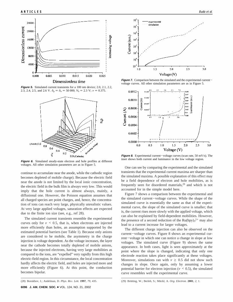
continue to accumulate near the anode, while the cathodic regionbecomes depleted of mobile charge). Because the electric fieldnear the anode is not limited by the local ionic concentration,the electric field in the bulk film is always very low. This wouldimply that the hole current is almost always, mainly, adiffusional one. However, the Poisson equation assumes thatall charged species are point charges, and, hence, the concentra-tion of ions can reach very large, physically unrealistic values.At very large applied voltages, saturation effects are expecteddue to the finite ion size (see, e.g., ref 28).
The simulated current transients resemble the experimentalcurves only forν < 0.5, that is, when electrons are injectedmore efficiently than holes, an assumption supported by theestimated potential barriers (see Table 1). Because only anionsare considered to be mobile, the asymmetry in the chargeinjection is voltage dependent. As the voltage increases, the layernear the cathode becomes totally depleted of mobile anions,because the injected electrons, having very large mobilities ascompared to the ions, are “expelled” very rapidly from this highelectric-field region. In this circumstance, the local concentrationhardly affects the electric field, and holes are injected more andmore efficiently (Figure 6). At this point, the conductionbecomes bipolar.
One can see by comparing the experimental and the simulatedtransients that the experimental current maxima are sharper thanthe simulated maxima. A possible explanation of this effect maybe a field dependence of electron and hole mobilities, as isfrequently seen for disordered materials,29 and which is notaccounted for in the simple model here.
Figure 7 shows a comparison between the experimental andthe simulated current-voltage curves. While the shape of thesimulated curve is essentially the same as that of the experi-mental curve, the slope of the simulated curve is smaller; thatis, the current rises more slowly with the applied voltage, whichcan also be explained by field-dependent mobilities. However,the presence of a second reduction of the Ru(bpy)3
2+ may alsolead to a current increase for larger voltages.
The different charge injection can also be observed on thecurrent-voltage curves. Figure 8 shows an experimental cur-rent-voltage in which one can notice a change in slope at lowvoltages. The simulated curve (Figure 9) shows the sameappearance. In both cases, light is seen approximately at thepoint where the slope is changed, indicating that only oneelectrode reaction takes place significantly at these voltages.Moreover, simulations ran withν g 0.5 did not show suchchanges in slope. Once again, only by assuming a lowerpotential barrier for electron injection (ν < 0.5), the simulatedcurve resembles well the experimental curve.
(28) Borukhov, I.; Andelman, D.Phys. ReV. Lett. 1997, 79, 435. (29) Brutting, W.; Berleb, S.; Mu¨ckl, A. Org. Electron.2001, 2, 1.
Figure 5. Simulated current transients for a 100 nm device; 2.0, 2.1, 2.2,2.3, 2.4, 2.5, and 2.6 V.δp ) δn ) 50 000;Vb ) 2.3 V; ν ) 0.375.
Figure 6. Simulated steady-state electron and hole profiles at differentvoltages. All other simulation parameters are as in Figure 5.
Figure 7. Comparison between the simulated and the experimental current-voltage curves. All other simulation parameters are as in Figure 5.
Figure 8. Experimental current-voltage curves (scan rate, 50 mV/s). Theinset shows both current and luminance in the low voltage region.
A R T I C L E S Buda et al.
6096 J. AM. CHEM. SOC. 9 VOL. 124, NO. 21, 2002

Figure 10 shows how the recombination profile changes withtime at 2.7 V. Note that the recombination maximum is, initially,very close to the anode and moves toward the middle of thefilm as holes start to inject more efficiently. However, due tothe different charge injection at the electrodes, the steady-staterecombination profile is still not located exactly in the middleof the film, even though we assumed the mobilities of electronsand holes to be identical.
For applied voltages larger than ca. 2.7 V, the electric fieldin the bulk film can be large enough to make the migrationcontribution to the current important at steady state. Simulationresults show that the hole profiles are almost perfect straightlines, indicating that the hole current is almost purely diffusional.This is due to the continuous rise of the electric field as a resultof anion accumulation near the anode, as previously discussed.In the case of electrons, the profiles are, however, quite differentand cannot be considered as straight lines, showing thatmigration is more important in this case.
It is difficult to obtain more quantitative estimates from thismodel since little is known about the properties of these films.For example, the model would correctly predict an increase ofquantum efficiency as the voltage increases (due to changingfrom unipolar to bipolar behavior), up to a maximum internalquantum efficiency of 4.6% (based on the fluorescence quantum
efficiency of Ru(bpy)32+ at room temperature), but it does notpredict a decrease once the conduction becomes bipolar (asexperimentally observed). If one would refine the model andtake into account the second and third reduction of Ru(bpy)3
2+,as well as side reactions and quenching effects due to theoxidized and reduced species and traces of water present in thefilm, the decrease in quantum efficiency may be predicted aswell, but at the expense of introducing more parameters thatare very difficult to estimate or measure. On the other hand,even for the simple model presented here, it is difficult to findgood estimates for parameters, and some of the estimates relyon data obtained in solution. For example, the steady-statecurrent depends both on the band gap and on the concentrationof mobile ions. A difference of 100 mV in determining the band-gap value, which is within the precision of the estimates, canlead to large changes in the steady-state current. Moreover, theconcentration of mobile ions, which is extremely difficult toestimate, determines the magnitude of the electric fields nearthe electrodes and hence the concentration of injected electronsand holes. This also affects, critically, the steady-state currentand luminescence. Nevertheless, we believe that the abovesimulation results aid in a better understanding of the behaviorof these devices.
Conclusions
It is shown that the behavior of tris(2,2′-bipyridine)ruthenium-(II)-based light-emitting devices depends strongly on the natureof mobile ions. Moreover, traces of water in the tris(2,2′-bipyridine)ruthenium(II) film seem to be intimately linked tothe existence of mobile ions.
A simple semiquantitative electrochemical model is proposedfor describing both the transient and the steady-state behaviorof light-emitting devices based on tris(2,2′-bipyridine)ruth-enium(II) and light-emitting electrochemical cells in general.The model describes well the transient behavior of theseelectroluminescent devices, proving that they are, in fact, light-emitting electrochemical cells.
The experimental data correlated with the simulation’s resultsindicate that for low applied voltages, electrons are the maincarriers in tris(2,2′-bipyridine)ruthenium(II) light-emitting de-vices, while for larger voltages, the device becomes bipolar.
Acknowledgment. Support by MURI (DAAD19-01-1-0676),The Center for Nano- and Molecular Science and Technology,and The Robert A. Welch Foundation is acknowledged. Theauthors wish to thank Stephen Feldberg (Brookhaven NationalLaboratory) for helpful discussions and David Saunders (NASAAmes Research Center) for providing several Fortran routines.
Appendix
All equations were rewritten in dimensionless form. Thedimensionless parameters and variables are film thickness,L;diffusion coefficient of the anions,Da; time, t; initial concentra-tion of mobile anions,ca
0; hole and electron concentrations,respectively,cp, cn; electric potential,Φ; dielectric permittivityof vacuum and the relative dielectric constant of the film,respectively,ε0, ε; second-order recombination rate constant,k; dimensionless space coordinate,ê ) x/L; dimensionless timecoordinate,τ ) Dat/L2; dimensionless concentrations for coun-
Figure 9. Simulated current-voltage curves (scan rate, 50 mV/s; all otherparameters are as in Figure 5). The inset shows both current and luminancein the low voltage region.
Figure 10. Simulated recombination profiles as a function of time at 2.7V. All simulation parameters are as in Figure 5.
Thin-Film Solid-State Electroluminescent Devices A R T I C L E S
J. AM. CHEM. SOC. 9 VOL. 124, NO. 21, 2002 6097
terions, holes, and electrons, respectively,a ) ca/ca0, p ) cp/ca
0,n ) cn/ca
0; dimensionless electric potential,æ ) F/RT× F; theratio between the diffusion coefficients of holes and anions andelectrons and anions, respectively,δp ) Dp/Da, δn ) Dn/Da;dimensionless recombination rate constant,R ) kca
0L2/Da;dimensionless parameter related to the Debye length,κ ) F 2L2
ca0/RTεε0; dimensionless current,I ) ∑i)p,n,a fi - (1/κ)(∂/∂τ)
(∂æ/∂ê), where I ) IL/(FDaca0A), A is the contact area, andfi
are the dimensionless fluxes (eq 5).
Supporting Information Available: Discretization and nu-merical model (PDF). This material is available free of chargevia the Internet at http://pubs.acs.org.
JA017834H
A R T I C L E S Buda et al.
6098 J. AM. CHEM. SOC. 9 VOL. 124, NO. 21, 2002
1
Supporting Information:
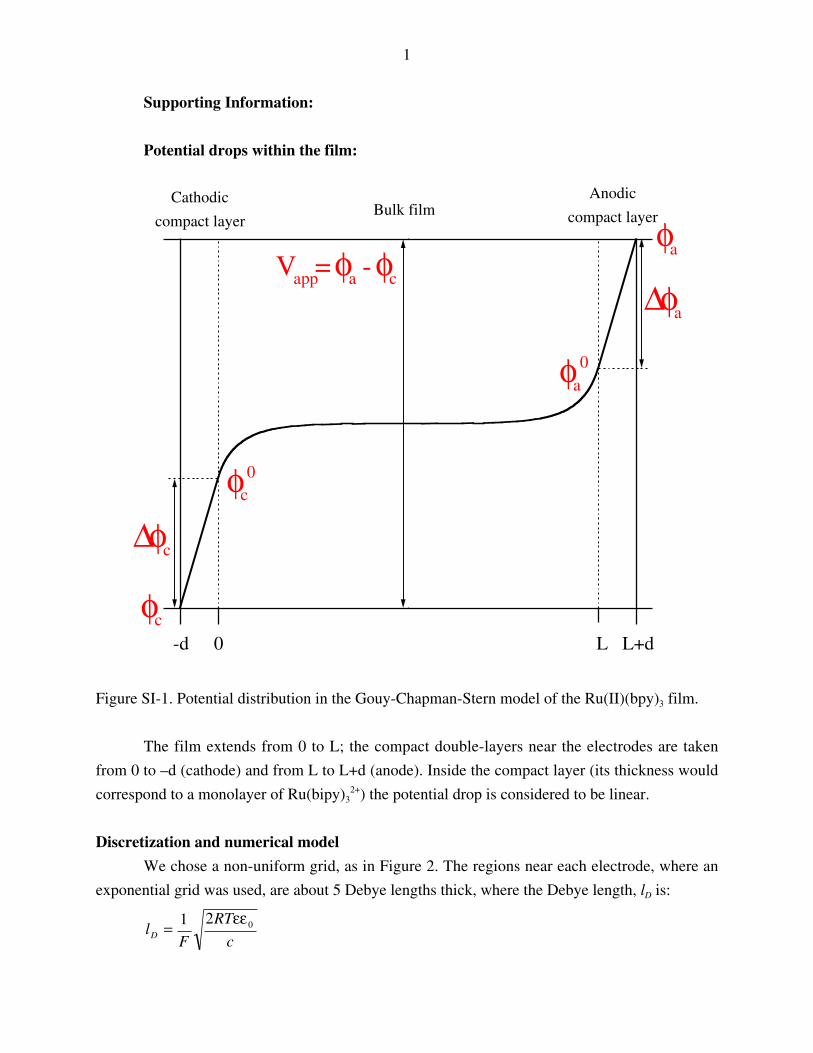
Potential drops within the film:
-d 0 L+dL
Vapp= φa - φc
∆φa
∆φc
φa0
φc0
φa
φc
Figure SI-1. Potential distribution in the Gouy-Chapman-Stern model of the Ru(II)(bpy)3 film.
The film extends from 0 to L; the compact double-layers near the electrodes are taken
from 0 to –d (cathode) and from L to L+d (anode). Inside the compact layer (its thickness would
correspond to a monolayer of Ru(bipy)32+) the potential drop is considered to be linear.
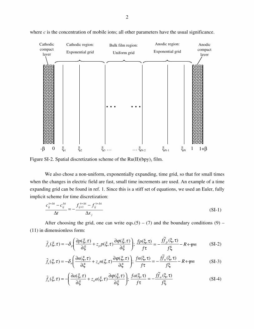
Discretization and numerical model
We chose a non-uniform grid, as in Figure 2. The regions near each electrode, where an
exponential grid was used, are about 5 Debye lengths thick, where the Debye length, lD is:
c
RT
FlD
021 εε=
Bulk filmAnodic
compact layerCathodic
compact layer
2
where c is the concentration of mobile ions; all other parameters have the usual significance.
Figure SI-2. Spatial discretization scheme of the Ru(II)(bpy)3 film.
We also chose a non-uniform, exponentially expanding, time grid, so that for small times
when the changes in electric field are fast, small time increments are used. An example of a time
expanding grid can be found in ref. 1. Since this is a stiff set of equations, we used an Euler, fully
implicit scheme for time discretization:
j
ijijijij
x
ff
t
cc
∆−
−=∆− τ∆+ττ∆+τ
+τ∆τ∆+τ
1(SI-1)
After choosing the grid, one can write eqs.(5) – (7) and the boundary conditions (9) –
(11) in dimensionless form:
˜ ( , )( , )
( , )( , )
fp
z pp p pξ τ δ ξ τξ
ξ τ ϕ ξ τξ
= − ∂∂
+ ∂∂
; pnRfp p ↔−
ξƒτξƒ
−=τƒτξƒ ),(
~),(
(SI-2)
˜ ( , )( , )
( , )( , )
fn
z nn n nξ τ δ ξ τξ
ξ τ ϕ ξ τξ
= − ∂∂
+ ∂∂
; pnRfn n ↔−
ξƒτξƒ
−=τƒτξƒ ),(
~),(
(SI-3)
˜ ( , )( , )
( , )( , )
fa
z aa aξ τ ξ τξ
ξ τ ϕ ξ τξ
= − ∂∂
+ ∂∂
; ξƒ
τξƒ−=
τƒτξƒ ),(
~),( afa
(SI-4)
0 ξ1 ξ2 ξ3 … 1ξNξN-1… ξN-2
… …
-β 1+β
Cathodiccompact
layer
Anodiccompact
layer
Cathodic region:
Exponential grid
Anodic region:
Exponential grid
Bulk film region:
Uniform grid

3
)2(),(
2
2
−+−κ=ξƒ
τξϕƒapn (SI-5)
where ξ = x/L; τ = Dat/L2; a = ca/ca
0; p = cp/ca0; n = cn/ca
0; ϕ = F/RT×Φ; δp = Dp/Da; δn = Dn/Da; R
= kca0L2/Da; κ = F2L2ca
0/RTεε0 (ca0 represents the concentration of mobile anions).
The dimensionless current is given by:
˜ ˜, ,
I fii p n a
= − ∂∂
∂∂
=
∑ 1κ τ
ϕξ
(SI-6)
where I~ = IL/(FDaca0A) and A is the contact area. Note that the total current is negative, but its
sign is just a matter of convention.
The dimensionless form of the boundary conditions are given by:
∆ϕ ϕ ϕ δδc c
c
c
n t p t
n t
p t
n t p t= − = + − −
= +
− −
0
0 00
00 0
e ec0
a0ln
( , ) ( , )( , )
ln( , )
( , ) ( , )(SI-7)
∂∂
− × ∂∂
== =
aa
( , )( , )
( , )ξ τξ
τ ϕ ξ τξξ ξ0 0
0 0 (SI-8)
∂∂
= −
=
ϕξ
ϕ ϕβξ 0
0 c (SI-9)
∆ϕ ϕ ϕ δδa a
c
c
n t p t
n t
p t
n t p t= − = + − −
= +
− −
+N c
0a0e e1
1 11
11 1
ln( , ) ( , )
( , )ln
( , )( , ) ( , )
(SI-10)
∂∂
− × ∂∂
== =
aa
( , )( , )
( , )ξ τξ
τ ϕ ξ τξξ ξ1 1
1 0 (SI-11)
∂∂
= −
=
+ϕξ
ϕ ϕβξ 1
1a N (SI-12)
where δc = c*/ca0 and β = d/L (c* is the total concentration of the Ru(bipy)2+ sites).
For calculating the excited-state concentration profiles with time, one more equation is
needed (written in dimensionless form):
γ↔−↔+ξƒγƒδ=
τƒγƒ
γ kpnR2
2
(SI-13)
where γ is the dimensionless excited state concentration (c*/ca0), δγ is the dimensionless diffusion
coefficient of the excite state (D*/Da) and k is the dimensionless decay constant of the excited
state (kd×L2/Da).
However, this equation can be solved independently once the electron and hole profiles
are known and does not require special treatment. The total electroluminescent light (expressed

4
as number of photons per second) coming out from the film will be:
P NAD c
Lk ydA
a a= × ∫0
0
1ξ (SI-14)
where NA is Avogadro’s number.
A classical discretization scheme does not work for this problem: the electric fields near
the electrodes (mostly near the anode, where mobile anions can accumulate; near the cathode, a
classical scheme might be used, although a large number of points are still needed) change very
rapidly with distance, and the classical discretization scheme fails (even 2000 points in the
anodic region are not enough to achieve convergence). Therefore, one needs to carefully choose
the numerical procedure. One of the most successful and widely used for semiconductor
simulations is the Scharfetter-Gummel discretization procedure, which works very well for very
large electric fields (although it fails when the electric field is very low). The Scharfetter-
Gummel method does not evaluate the partial derivatives of concentrations and potential as first
order approximations in one box, but instead assumes that within one box all the fluxes and the
electric field are constant. For example, in the flux equation for holes:
˜ ( , )( , )
( , )( , )
fp
z pp p pξ τ δ ξ τξ
ξ τ ϕ ξ τξ
= − ∂∂
+ ∂∂
if the flux ),(~ τξpf and
ξƒτξϕƒ= ),(~e are constant, then one can integrate the flux equation in one
box:
˜ ˜fdp
dz pep p p= − +
δξ
; −+
= = −+ +
+∫ ∫dp
z pe fd
p p pj
j
j
j
j j˜ ˜ /δξ ξ ξ
1 1
1
and obtains:
˜˜
exp( ˜( ))
exp( ˜( )) exp( ˜( ))
fz e
p z e
z e
p
z ep
pp
j p j j
p j j
j
p j jδξ ξξ ξ ξ ξ
=× − −− − −
−− − −
+
+
+
+
1
1
1
11 1 =
= −− −
+− − −
+
+
+
z ep
z e
p
z epj
p j j
j
p j j
˜exp( ˜( )) exp( ˜( ))1 11
1
1ξ ξ ξ ξ
By replacing jj
jjeξ−ξϕ−ϕ
=ξƒϕƒ=
+
+
1
1~ , eq. (15) is obtained:
˜, ( ) ( )f z
p
e
p
ep j p pj j
j j
jz
jzp j j p j j
= −−−
×−
+−
+
+
+− − −+ +
δϕ ϕξ ξ ϕ ϕ ϕ ϕ
1
1
1
1 11 1(SI-15)
Similar expressions can be written for electrons and mobile anions just by changing the
letter p with n and a respectively. Note that this procedure does not work if one uses the (more
general) Savéant equations for the fluxes: by integrating the flux equation a transcedental
5
equation is obtained, from which an analytical expression for the flux cannot be obtained. If,
however, the carrier concentrations are small compared to the total concentration of redox sites,
using the Nernst-Planck equations is a good approximation.
By using this scheme, one achieves very good convergence and accuracy for large fields;
in fact 200 grid points (50 near each electrode and 100 for the bulk) may be enough for most
situations (depending on the concentration of mobile ions: for large concentrations, a larger
number of grid points might be needed). One can easily notice that this procedure fails if the
electric field is very low: the exponentials in the flux expression tend to 1 when the electric field
is small, and a division by zero occurs. Depending on the precision with which the exponential is
evaluated, the lowest voltage value at which the algorithm is still usable may vary. In our case,
the algorithm ceases to work for applied voltages lower than ~0.6 V. A series expansion of the
exponentials in eq. SI-15 may extend the validity region for small voltages too.
The flux equations are then replaced in eq. (SI-1) written in dimensionless form. One
obtains a set of equations that can be written as:
Fjϕ(ϕ, n, p, a) = 0 (SI-16)
Fjn(ϕ, n, p, a) = 0 (SI-17)
Fjp(ϕ, n, p, a) = 0 (SI-18)
Fja(ϕ, n, p, a) = 0 (SI-19)
where the j index represents the j-th grid point, while index i = ϕ , n, p, a indicate the variable
(potential, and chemical species). For the first and the last grid points, the boundary conditions
(SI-7) to (SI-12) are replaced in the expressions of each F1i and FNi, so one obtains a system of
non-linear equations of order 4N (N is the number of the grid-points; the cathode is chosen at
grid point 0 and the anode at N+1). Now one can choose a method for solving this system: the
most widely used is the Newton-Raphson method, which ensures fast convergence. If one has a
system of equations written as:
F(X) = 0 (SI-20)
where F is the functions vector and X is the variables vector, then at each iteration, k, the
solution is improved by using the following procedure:
Xk+1 = Xk + ∆Xk; ∆Xk = -(Jk)-1×Fk (SI-21)
where J is the Jacobian matrix:
6
J =
∂∂
∂∂
∂∂
∂∂
∂∂
∂∂
∂∂
∂∂
∂∂
F
X
F
X
F
XF
X
F
X
F
X
F
X
F
X
F
X
N
N
N N N
N
1
1
1
2
1
2
1
2
2
2
1 2
...
...
... ... ... ...
...
(SI-22)
The easiest way to use the Newton-Raphson for this kind of problem is to use the solution
from the previous time moment as an initial guess (for the first time step, the initial condition is
used as a guess) and improve the solution until ∆Xji∑ is less than some expected tolerance
value. For our specific problem, the F vector represents the set of equations (SI-16) through (SI-
19), and the variables vector X represents the potential, electron hole and anion concentrations at
each grid-point (ϕj, nj, pj, aj).
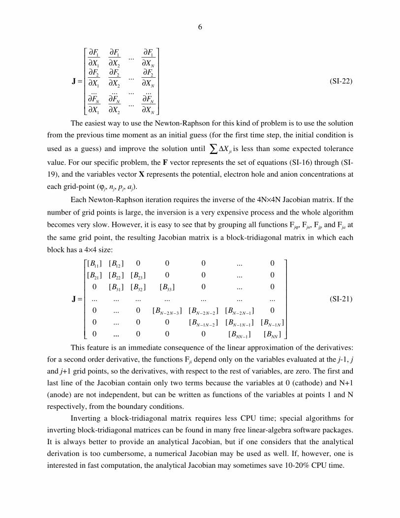
Each Newton-Raphson iteration requires the inverse of the 4N×4N Jacobian matrix. If the
number of grid points is large, the inversion is a very expensive process and the whole algorithm
becomes very slow. However, it is easy to see that by grouping all functions Fjϕ, Fjn, Fjp and Fja at
the same grid point, the resulting Jacobian matrix is a block-tridiagonal matrix in which each
block has a 4×4 size:
J =
− − − − − −
− − − − −
[ ] [ ] ...
[ ] [ ] [ ] ...
[ ] [ ] [ ] ...
... ... ... ... ... ... ...
... [ ] [ ] [ ]
... [ ] [ ] [ ]
B B
B B B
B B B
B B B
B B BN N N N N N
N N N N N N
11 12
21 22 23
31 32 33
2 3 2 2 2 1
1 2 1 1 1
0 0 0 0
0 0 0
0 0 0
0 0 0
0 0 0
0 ...... [ ] [ ]0 0 0 1B BNN NN−
(SI-21)
This feature is an immediate consequence of the linear approximation of the derivatives:
for a second order derivative, the functions Fji depend only on the variables evaluated at the j-1, j
and j+1 grid points, so the derivatives, with respect to the rest of variables, are zero. The first and
last line of the Jacobian contain only two terms because the variables at 0 (cathode) and N+1
(anode) are not independent, but can be written as functions of the variables at points 1 and N
respectively, from the boundary conditions.
Inverting a block-tridiagonal matrix requires less CPU time; special algorithms for
inverting block-tridiagonal matrices can be found in many free linear-algebra software packages.
It is always better to provide an analytical Jacobian, but if one considers that the analytical
derivation is too cumbersome, a numerical Jacobian may be used as well. If, however, one is
interested in fast computation, the analytical Jacobian may sometimes save 10-20% CPU time.

7
A complete algorithm for solving the above presented problem may look as follows:
[1]. Choose a spatial grid and calculate the grid points;
[2]. Choose a time grid;
[3]. For each increment ∆τ, take the solution at time step τ and perform one Newton-
Raphson iteration;
[4]. Calculate the ∆X vector and compare ∆Xji∑ with the tolerance;
[5]. If ∆Xji∑ is larger than the desired tolerance, calculate the new solution vector, X,
from eq. (SI-21) and go back to [3]. If ∆Xji∑ is less than the desired tolerance, keep the
solution vector X as the final solution for time τ + ∆τ;
[6] Calculate currents, electric fields and other needed quantities for time τ
[7] Go back to [3] to further increment the time, and use the values for time τ as initial
guess until the final desired time value is reached.
The best and easiest way to check the results is to calculate the total current (eq. SI-6): it
can be shown that the total current must be position independent, i.e. the total current is a
function of time only. If the results do not show a constant total current throughout the film, the
program needs to be checked.
Some other results obtained from the simulation are also shown below:
Figure SI-3. Simulated electric field profile within the film at 3.0 V. All other simulation
parameters as in Figure 5 from manuscript.

8
Figure SI-4. Simulated electron and hole profiles as function of time at 3.0 V. All other
simulation parameters as in Figure 5 from manuscript.
Figure SI-5. Experimental and simulated quantum efficiencies as a function of voltage. All
simulation parameters as in Figure 5 from manuscript. Inset shows the same plot, but on a
logarithmic scale.
Reference

9
1 T. R. Brumleve and R. P. Buck, J. Electroanal. Chem., 1978, 90, 1.