Thin Film Photovoltaics: Advances in Earth Abundant ...€¦ · Thin Film Photovoltaics: Advances...
54
Thin Film Photovoltaics: Advances in Earth Abundant Chalcogenide Technologies Victor Izquierdo-Roca 1 , Edgardo Saucedo 1 , Alejandro Pérez-Rodríguez 1,2 IREC, Catalonia Institute for Energy Research, Barcelona, Spain 2IN2UB, Departament d’Electrònica, Universitat de Barcelona, Barcelona, Spain e-mail: [email protected] UNSW SPREE School Seminar, October 2016. Paul Pistor 1
Transcript of Thin Film Photovoltaics: Advances in Earth Abundant ...€¦ · Thin Film Photovoltaics: Advances...

Thin Film Photovoltaics: Advances in Earth Abundant Chalcogenide Technologies
Victor Izquierdo-Roca1, Edgardo Saucedo1, Alejandro Pérez-Rodríguez1,2
IREC, Catalonia Institute for Energy Research, Barcelona, Spain 2IN2UB, Departament d’Electrònica, Universitat de Barcelona, Barcelona, Spain
e-mail: [email protected] UNSW SPREE School Seminar, October 2016.
Paul Pistor1
1. Introduction 2. Objectives 3. Experimental 4. Results 5. Conclusions
Preface
Paul Pistor has received funding from the European Union’s Seventh
Framework Programme under reference number FP7-PEOPLE-2013-IEF-
625840 (“JumpKEST”)
Martin-Luther University
Halle-Wittenberg
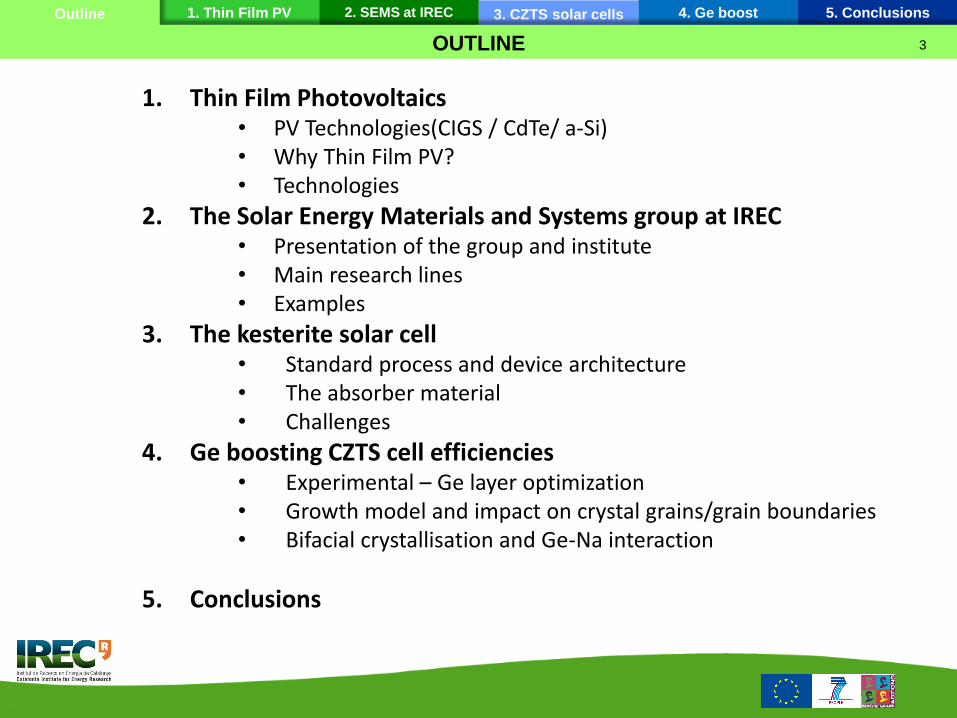
1. Thin Film PV 2. SEMS at IREC 3. CZTS solar cells 4. Ge boost 5. Conclusions
OUTLINE
Outline
1. Thin Film Photovoltaics • PV Technologies(CIGS / CdTe/ a-Si) • Why Thin Film PV? • Technologies
2. The Solar Energy Materials and Systems group at IREC • Presentation of the group and institute • Main research lines • Examples
3. The kesterite solar cell • Standard process and device architecture • The absorber material • Challenges
4. Ge boosting CZTS cell efficiencies • Experimental – Ge layer optimization • Growth model and impact on crystal grains/grain boundaries • Bifacial crystallisation and Ge-Na interaction
5. Conclusions
3
2. SEMS at IREC 3. CZTS solar cells 4. Ge boost 5. Conclusions Outline 1. Thin Film PV
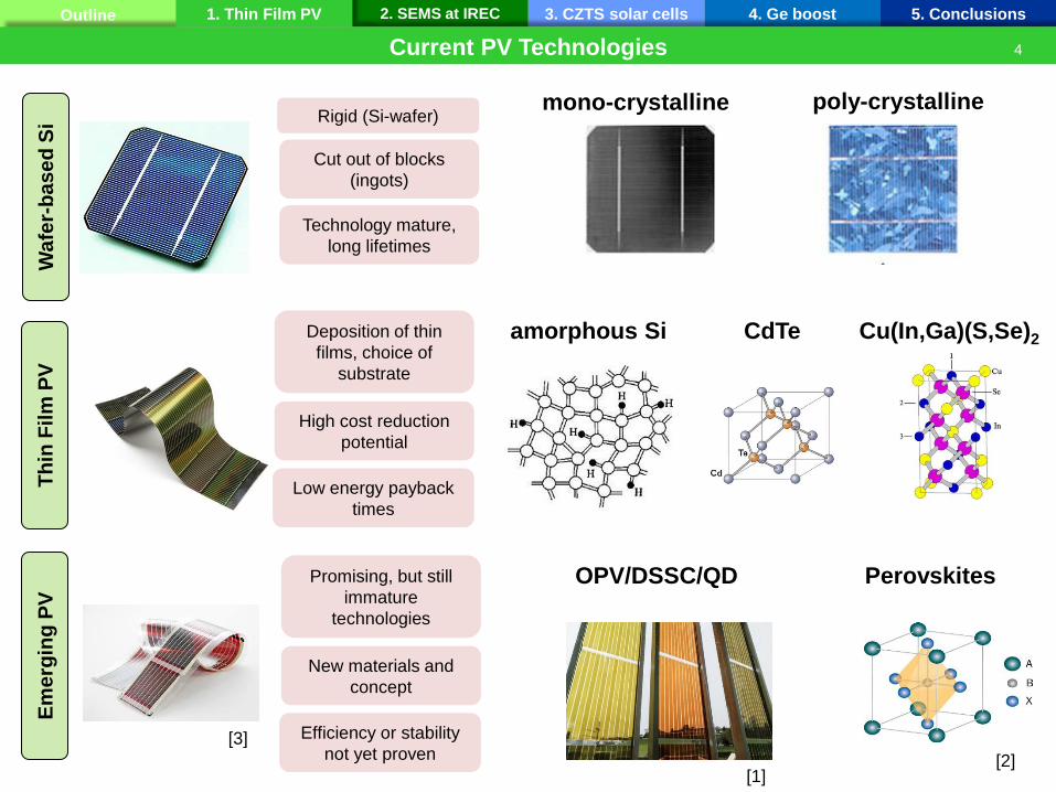
Current PV Technologies W
afe
r-b
as
ed
Si
Cut out of blocks
(ingots)
Technology mature,
long lifetimes
Rigid (Si-wafer) mono-crystalline poly-crystalline
Deposition of thin
films, choice of
substrate
High cost reduction
potential
Low energy payback
times
Th
in F
ilm
PV
amorphous Si CdTe Cu(In,Ga)(S,Se)2
[1] OPV solar windows at EPFL
[2] Thomas Leijtens, OPV Summit
[3] InfitinityPV www.infintiyPV.com
Em
erg
ing
PV
Promising, but still
immature
technologies
New materials and
concept
Efficiency or stability
not yet proven
OPV/DSSC/QD Perovskites
[2] [1]
[3]
4
2. SEMS at IREC 3. CZTS solar cells 4. Ge boost 5. Conclusions Outline 1. Thin Film PV
thin film 9.2%
monocrystalline 35.6%
multicrystalline 55.2%
Record lab cell efficiency
Record module efficiency
Highest commercial module eff. 2016
Global production in 2014+ [GWp]
Energy payback time* [years]
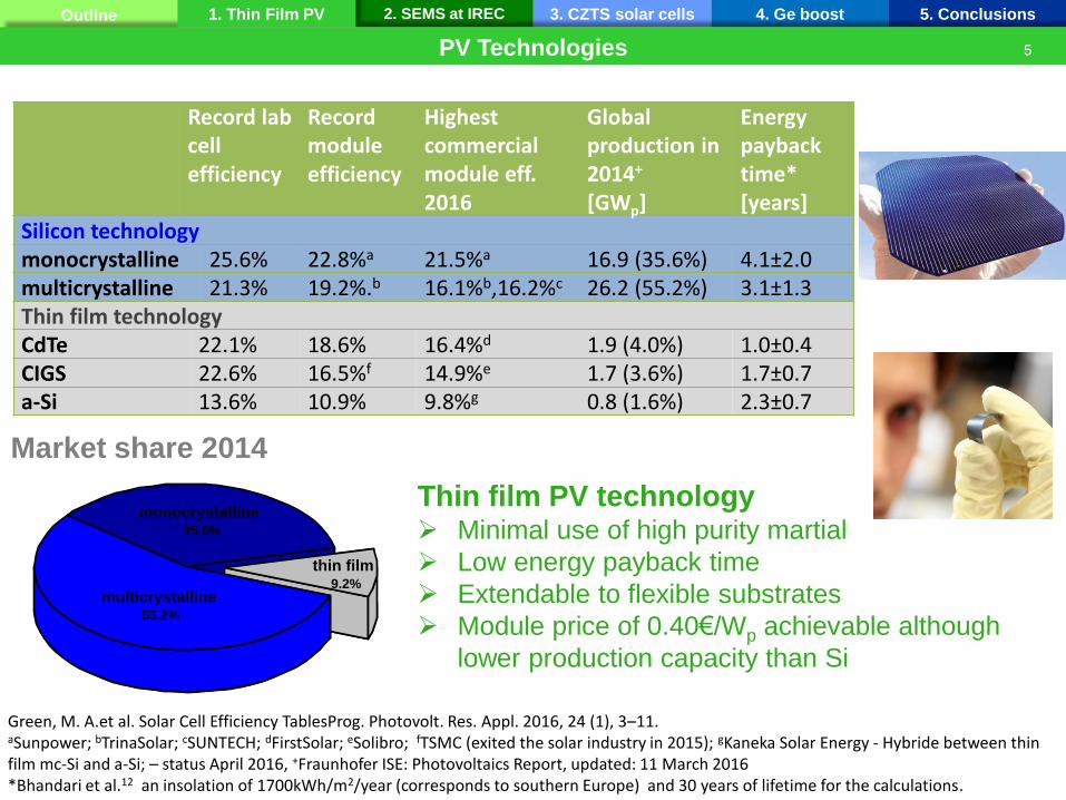
Silicon technology monocrystalline 25.6% 22.8%a 21.5%a 16.9 (35.6%) 4.1±2.0 multicrystalline 21.3% 19.2%.b 16.1%b,16.2%c 26.2 (55.2%) 3.1±1.3
Green, M. A.et al. Solar Cell Efficiency TablesProg. Photovolt. Res. Appl. 2016, 24 (1), 3–11. aSunpower; bTrinaSolar; cSUNTECH; dFirstSolar; eSolibro; fTSMC (exited the solar industry in 2015); gKaneka Solar Energy - Hybride between thin film mc-Si and a-Si; – status April 2016, +Fraunhofer ISE: Photovoltaics Report, updated: 11 March 2016 *Bhandari et al.12 an insolation of 1700kWh/m2/year (corresponds to southern Europe) and 30 years of lifetime for the calculations.
Market share 2014
Thin film PV technology Minimal use of high purity martial
Low energy payback time
Extendable to flexible substrates
Module price of 0.40€/Wp achievable although
lower production capacity than Si
Record lab cell efficiency
Record module efficiency
Highest commercial module eff. 2016
Global production in 2014+ [GWp]
Energy payback time* [years]
Silicon technology monocrystalline 25.6% 22.8%a 21.5%a 16.9 (35.6%) 4.1±2.0 multicrystalline 21.3% 19.2%.b 16.1%b,16.2%c 26.2 (55.2%) 3.1±1.3 Thin film technology CdTe 22.1% 18.6% 16.4%d 1.9 (4.0%) 1.0±0.4 CIGS 22.6% 16.5%f 14.9%e 1.7 (3.6%) 1.7±0.7 a-Si 13.6% 10.9% 9.8%g 0.8 (1.6%) 2.3±0.7
PV Technologies 5
2. SEMS at IREC 3. CZTS solar cells 4. Ge boost 5. Conclusions Outline 1. Thin Film PV
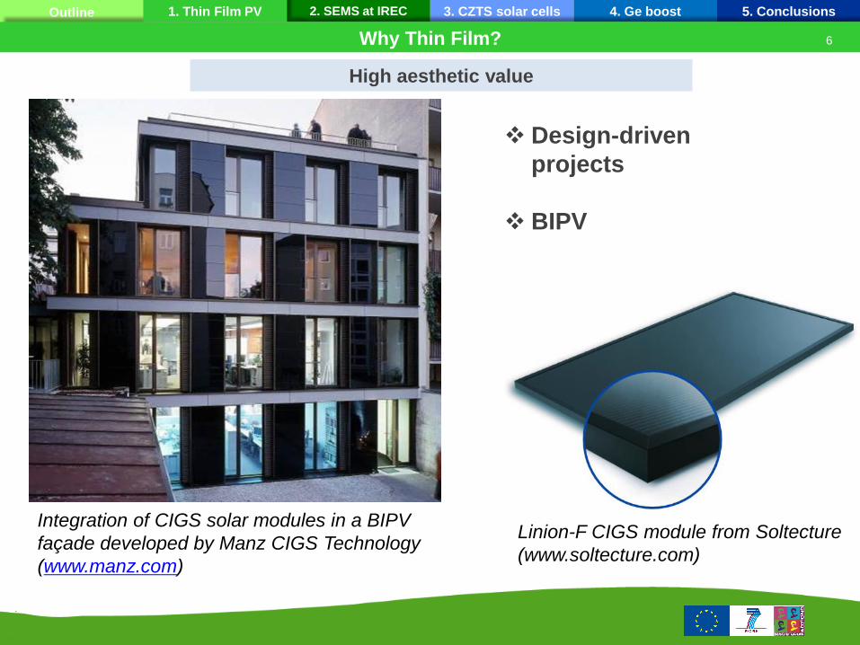
High aesthetic value
Design-driven
projects
BIPV
Why Thin Film?
Integration of CIGS solar modules in a BIPV
façade developed by Manz CIGS Technology
(www.manz.com)
Solibro SL2 module (up to 16%)
www.solibro-solar.com
Linion-F CIGS module from Soltecture
(www.soltecture.com)
6
2. SEMS at IREC 3. CZTS solar cells 4. Ge boost 5. Conclusions Outline 1. Thin Film PV
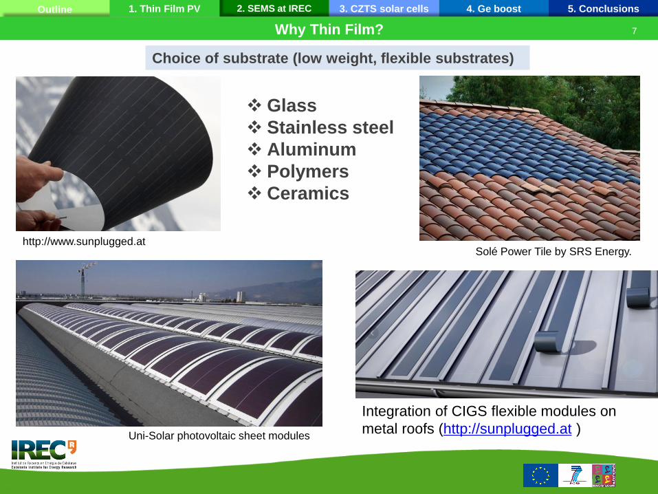
Choice of substrate (low weight, flexible substrates)
Glass
Stainless steel
Aluminum
Polymers
Ceramics
Why Thin Film?
Integration of CIGS flexible modules on
metal roofs (http://sunplugged.at )
http://www.sunplugged.at
Uni-Solar photovoltaic sheet modules
Solé Power Tile by SRS Energy.
7
2. SEMS at IREC 3. CZTS solar cells 4. Ge boost 5. Conclusions Outline 1. Thin Film PV
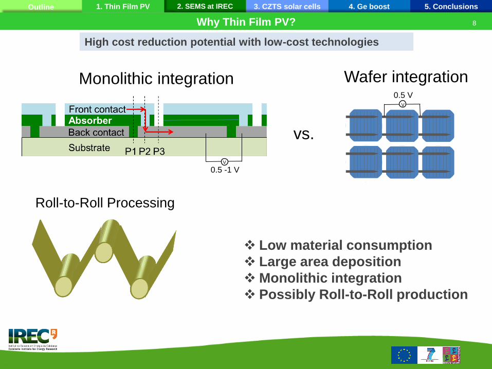
High cost reduction potential with low-cost technologies
P2 P3 Substrate P1
Absorber Front contact
Back contact
vs.
Monolithic integration Wafer integration
V
0.5 V
V
0.5 -1 V
Low material consumption
Large area deposition
Monolithic integration
Possibly Roll-to-Roll production
Roll-to-Roll Processing
Why Thin Film PV? 8
2. SEMS at IREC 3. CZTS solar cells 4. Ge boost 5. Conclusions Outline 1. Thin Film PV
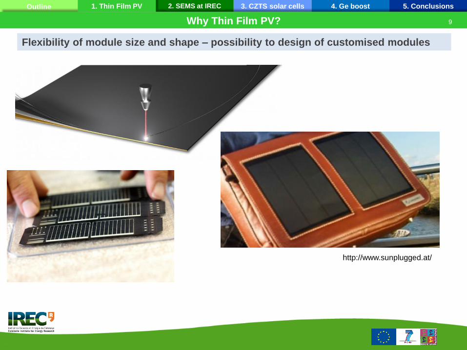
Flexibility of module size and shape – possibility to design of customised modules
http://www.sunplugged.at/
Why Thin Film PV? 9
2. SEMS at IREC 3. CZTS solar cells 4. Ge boost 5. Conclusions Outline 1. Thin Film PV
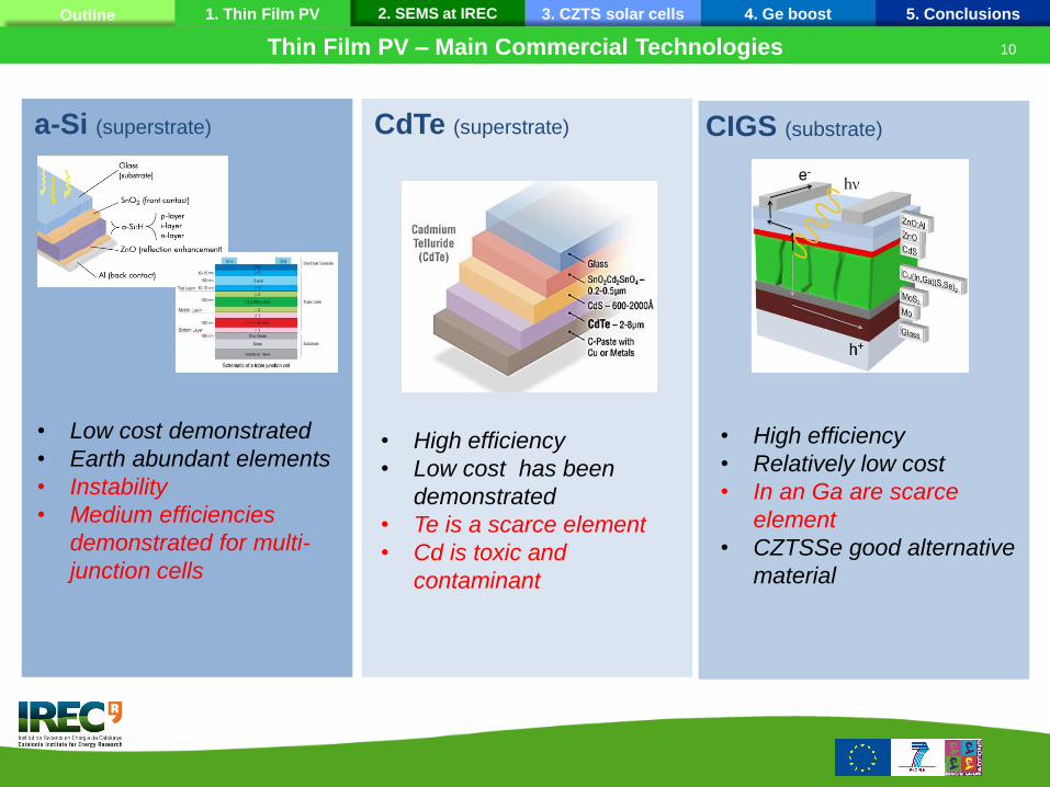
a-Si (superstrate)
CdTe (superstrate)
• High efficiency
• Low cost has been
demonstrated
• Te is a scarce element
• Cd is toxic and
contaminant
CIGS (substrate)
• High efficiency
• Relatively low cost
• In an Ga are scarce
element
• CZTSSe good alternative
material
• Low cost demonstrated
• Earth abundant elements
• Instability
• Medium efficiencies
demonstrated for multi-
junction cells
Thin Film PV – Main Commercial Technologies 10
3. CZTS solar cells 4. Ge boost 5. Conclusions Outline 1. Thin Film PV 2. SEMS at IREC
SEMS at IREC
1. Thin Film Photovoltaics • PV Technologies(CIGS / CdTe/ a-Si) • Why Thin Film PV? • Technologies
2. The Solar Energy Materials and Sytems group at IREC • Presentation of the group and institute • Main research lines • Examples
3. The kesterite solar cell • Standard process and device architecture • The absorber material • Challenges
4. Ge boosting CZTS cell efficiencies • Experimental – Ge layer optimization • Growth model and impact on crystal grains/grain boundaries • Bifacial crystallisation and Ge-Na interaction
5. Conclusions
11
10
3. CZTS solar cells 4. Ge boost 5. Conclusions Outline 1. Thin Film PV 2. SEMS at IREC
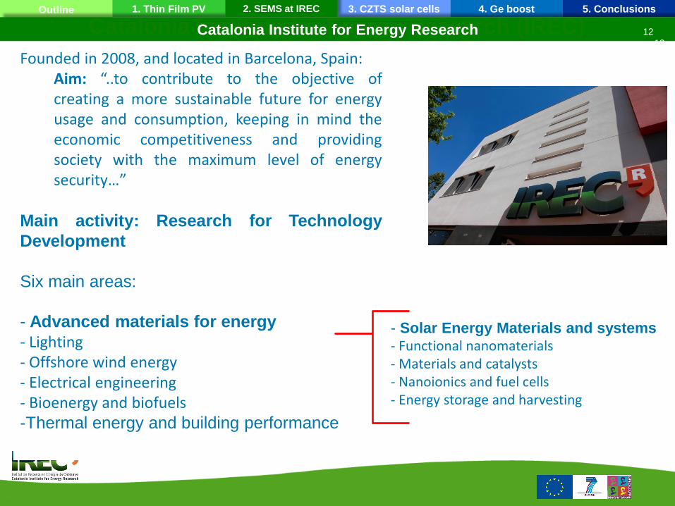
Catalonia Institute for Energy Research (IREC)
Founded in 2008, and located in Barcelona, Spain: Aim: “..to contribute to the objective of creating a more sustainable future for energy usage and consumption, keeping in mind the economic competitiveness and providing society with the maximum level of energy security…”
Main activity: Research for Technology
Development
Six main areas: - Advanced materials for energy - Lighting - Offshore wind energy - Electrical engineering - Bioenergy and biofuels -Thermal energy and building performance
Catalonia Institute for Energy Research
- Solar Energy Materials and systems - Functional nanomaterials - Materials and catalysts - Nanoionics and fuel cells - Energy storage and harvesting
12
12
3. CZTS solar cells 4. Ge boost 5. Conclusions Outline 1. Thin Film PV 2. SEMS at IREC
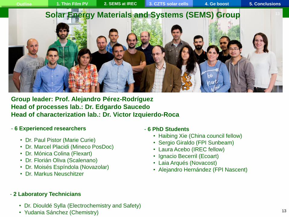
Solar Energy Materials and Systems (SEMS) Group
Group leader: Prof. Alejandro Pérez-Rodríguez
Head of processes lab.: Dr. Edgardo Saucedo
Head of characterization lab.: Dr. Victor Izquierdo-Roca
- 6 Experienced researchers
• Dr. Paul Pistor (Marie Curie)
• Dr. Marcel Placidi (Mineco PosDoc)
• Dr. Mónica Colina (Flexart)
• Dr. Florián Oliva (Scalenano)
• Dr. Moisés Espíndola (Novazolar)
• Dr. Markus Neuschitzer
13
- 6 PhD Students
• Haibing Xie (China council fellow)
• Sergio Giraldo (FPI Sunbeam)
• Laura Acebo (IREC fellow)
• Ignacio Becerril (Ecoart)
• Laia Arqués (Novacost)
• Alejandro Hernández (FPI Nascent)
- 2 Laboratory Technicians
• Dr. Diouldé Sylla (Electrochemistry and Safety)
• Yudania Sánchez (Chemistry) 13
3. CZTS solar cells 4. Ge boost 5. Conclusions Outline 1. Thin Film PV 2. SEMS at IREC
Solar Energy Materials and Systems
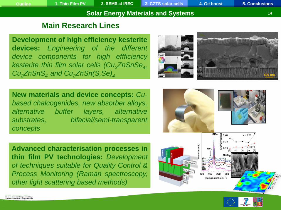
Main Research Lines
14
Mo2 and Mo3 similar SEM
MoA
MoB
MoSe2
500 nm
Mo4
Development of high efficiency kesterite
devices: Engineering of the different
device components for high effficiency
kesterite thin film solar cells (Cu2ZnSnSe4,
Cu2ZnSnS4 and Cu2ZnSn(S,Se)4
Advanced characterisation processes in
thin film PV technologies: Development
of techniques suitable for Quality Control &
Process Monitoring (Raman spectroscopy,
other light scattering based methods)
New materials and device concepts: Cu-
based chalcogenides, new absorber alloys,
alternative buffer layers, alternative
substrates, bifacial/semi-transparent
concepts
14
2. SEMS at IREC 3. CZTS solar cells 4. Ge boost 5. Conclusions Outline 1. Thin Film PV
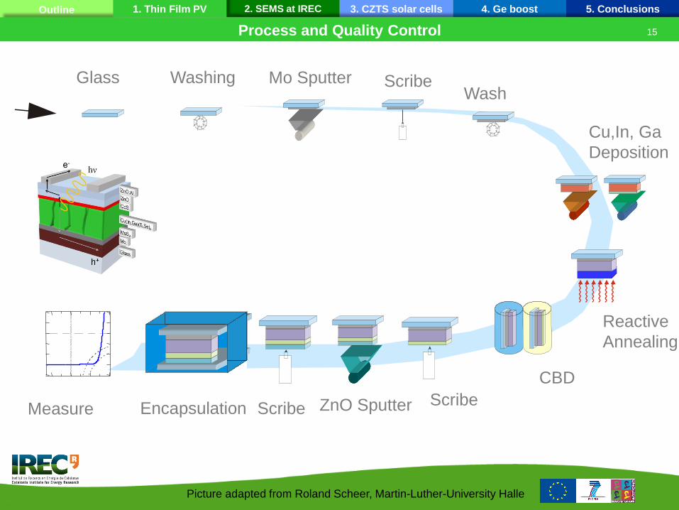
Process and Quality Control
Glass Washing Mo Sputter Scribe
Cu,In, Ga
Deposition
Reactive
Annealing
CBD
Scribe ZnO Sputter Scribe Encapsulation
Wash
Measure
Picture adapted from Roland Scheer, Martin-Luther-University Halle
15
3. CZTS solar cells 4. Ge boost 5. Conclusions Outline 1. Thin Film PV 2. SEMS at IREC
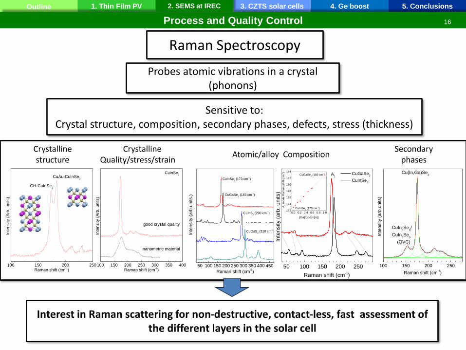
All these parameters are susceptible to be correlated with electrical properties of the PV devices [1]
Process and Quality Control
50 100 150 200 250 300 350 400 450
Inte
nsity (
arb
.un
its.)
Raman shift (cm-1)
CuGaS2 (310 cm
-1)
CuInS2 (290 cm
-1)
CuGaSe2 (183 cm
-1)
CuInSe2 (173 cm
-1)
Atomic/alloy Composition Crystalline structure
100 150 200 250
CH-CuInSe2
Inte
nsity (
Arb
. units)
Raman shift (cm-1)
CuAu-CuInSe2
100 150 200 250 300 350 400
CuInSe2
nanometric material
Inte
nsity (
Arb
. units)
Raman shift (cm-1)
good crystal quality
Crystalline Quality/stress/strain
50 100 150 200 250
0.0 0.2 0.4 0.6 0.8 1.0172
174
176
178
180
182
184
Inte
nsity (
arb
. u
nits)
Raman shift (cm-1)
CuGaSe2
CuInSe2
A1
CuGaSe2 (183 cm
-1)
A1 m
od
e R
am
an
sh
ift (c
m-1)
[Ga]/([Ga]+[In])
CuInSe2 (173 cm
-1)
Secondary phases
100 150 200 250
Cu(In,Ga)Se2
Inte
nsity (
arb
.units)
Raman shift (cm-1)
CuIn5Se
8/
CuIn3Se
5
(OVC)
Raman Spectroscopy
Probes atomic vibrations in a crystal (phonons)
Sensitive to: Crystal structure, composition, secondary phases, defects, stress (thickness)
Interest in Raman scattering for non-destructive, contact-less, fast assessment of the different layers in the solar cell
16
3. CZTS solar cells 4. Ge boost 5. Conclusions Outline 1. Thin Film PV 2. SEMS at IREC
Alternative substrates
Substrates and applications
Soda-lime Glass
Flexible modules
• Mechanical properties
• Thermal properties
• Alkali (Na, K)
High efficiency
traditional
modules
WR 12.6%
IREC 10.6%
Building-
integrated PV
• Non-flat
• No alkali
• lmpurities
Roll-to-roll
Alternative
Numerous applications!
Ceramic Steel Polyimide
• Rough
• No alkali
• lmpurities
• Non-rigid
• No alkali
• Low T
17
3. CZTS solar cells 4. Ge boost 5. Conclusions Outline 1. Thin Film PV 2. SEMS at IREC
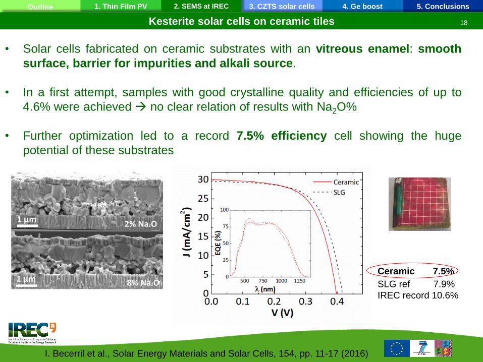
Kesterite solar cells on ceramic tiles
• Solar cells fabricated on ceramic substrates with an vitreous enamel: smooth
surface, barrier for impurities and alkali source.
• In a first attempt, samples with good crystalline quality and efficiencies of up to
4.6% were achieved no clear relation of results with Na2O%
• Further optimization led to a record 7.5% efficiency cell showing the huge
potential of these substrates
Ceramic 7.5%
SLG ref 7.9%
IREC record 10.6%
I. Becerril et al., Solar Energy Materials and Solar Cells, 154, pp. 11-17 (2016)
18
3. CZTS solar cells 4. Ge boost 5. Conclusions Outline 1. Thin Film PV 2. SEMS at IREC
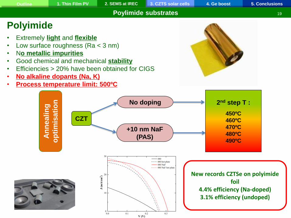
Poylimide substrates
• Extremely light and flexible
• Low surface roughness (Ra < 3 nm)
• No metallic impurities
• Good chemical and mechanical stability
• Efficiencies > 20% have been obtained for CIGS
• No alkaline dopants (Na, K)
• Process temperature limit: 500ºC
Polyimide
New records CZTSe on polyimide foil
4.4% efficiency (Na-doped) 3.1% efficiency (undoped)
CZT
No doping 2nd step T :
450ºC
460ºC
470ºC
480ºC
490ºC
+10 nm NaF
(PAS) An
neali
ng
op
tim
isati
on
19
3. CZTS solar cells 4. Ge boost 5. Conclusions Outline 1. Thin Film PV 2. SEMS at IREC
CZTS solar cells at IREC
1. Thin Film Photovoltaics • PV Technologies(CIGS / CdTe/ a-Si) • Why Thin Film PV? • Technologies
2. The SEMS group at IREC • Presentation of the group and institute • Main research lines • Examples
3. The kesterite solar cell • Standard process and device architecture • The absorber material • Challenges
4. Ge boosting CZTS cell efficiencies • Experimental – Ge layer optimization • Growth model and impact on crystal grains/grain boundaries • Bifacial crystallisation and Ge-Na interaction
5. Conclusions
20
20
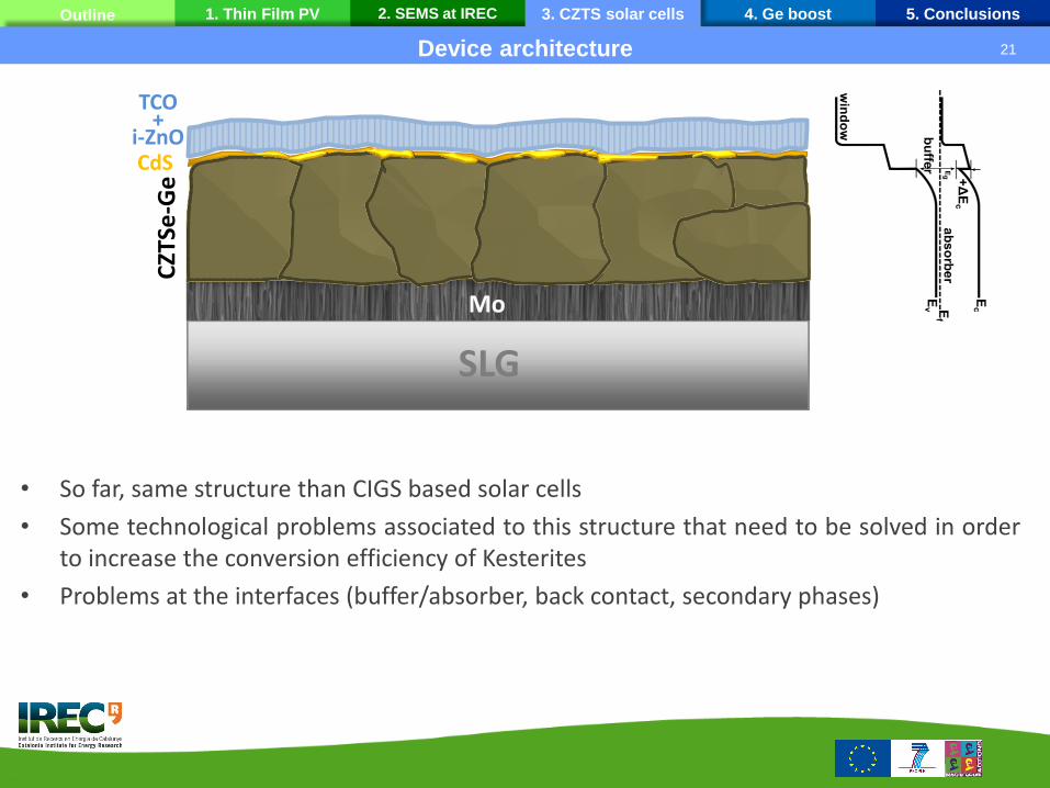
4. Ge boost 5. Conclusions Outline 1. Thin Film PV 2. SEMS at IREC 3. CZTS solar cells
Cu/Sn/Cu/Zn
Ge nano-layer
SLG
Mo
CZT
Se-G
e CdS
TCO +
i-ZnO
• So far, same structure than CIGS based solar cells
• Some technological problems associated to this structure that need to be solved in order to increase the conversion efficiency of Kesterites
• Problems at the interfaces (buffer/absorber, back contact, secondary phases)
Device architecture 21
4. Ge boost 5. Conclusions Outline 1. Thin Film PV 2. SEMS at IREC 3. CZTS solar cells
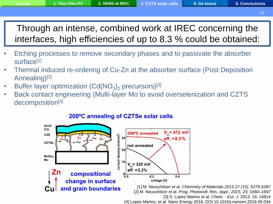
Through an intense, combined work at IREC concerning the
interfaces, high efficiencies of up to 8.3 % could be obtained:
• Etching processes to remove secondary phases and to passivate the absorber
surface[1]
• Thermal induced re-ordering of Cu-Zn at the absorber surface (Post Deposition
Annealing)[2]
• Buffer layer optimization (Cd(NO3)2 precursors)[3]
• Back contact engineering (Multi-layer Mo to avoid overselenization and CZTS
decomposition[4]
[1] M. Neuschitzer et al. Chemistry of Materials 2015 27 (15), 5279-5287
[2] M. Neuschitzer et al. Prog. Photovolt: Res. Appl., 2015, 23: 1660–1667
[3] S. Lopez-Marino et al. Chem. - Eur. J. 2013, 19, 14814
[4] Lopez-Marino, et al. Nano Energy 2016, DOI:10.1016/j.nanoen.2016.06.034
22
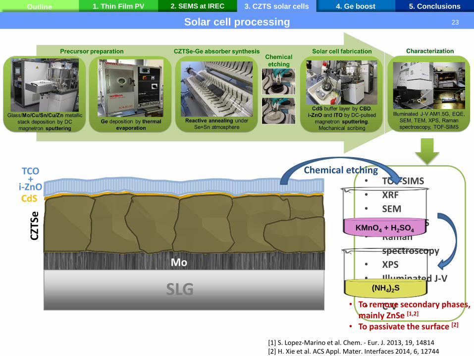
4. Ge boost 5. Conclusions Outline 1. Thin Film PV 2. SEMS at IREC 3. CZTS solar cells
• TOF-SIMS
• XRF
• SEM
• TEM - EELS
• Raman
spectroscopy
• XPS
• Illuminated J-V
• EQE
• C-V
KMnO4 + H2SO4
Chemical etching
Cu/Sn/Cu/Zn
Ge nano-layer
SLG (NH4)2S
Mo
CZT
Se
CdS
TCO +
i-ZnO
• To remove secondary phases, mainly ZnSe [1,2]
• To passivate the surface [2]
[1] S. Lopez-Marino et al. Chem. - Eur. J. 2013, 19, 14814 [2] H. Xie et al. ACS Appl. Mater. Interfaces 2014, 6, 12744
Solar cell processing 23
4. Ge boost 5. Conclusions Outline 1. Thin Film PV 2. SEMS at IREC 3. CZTS solar cells
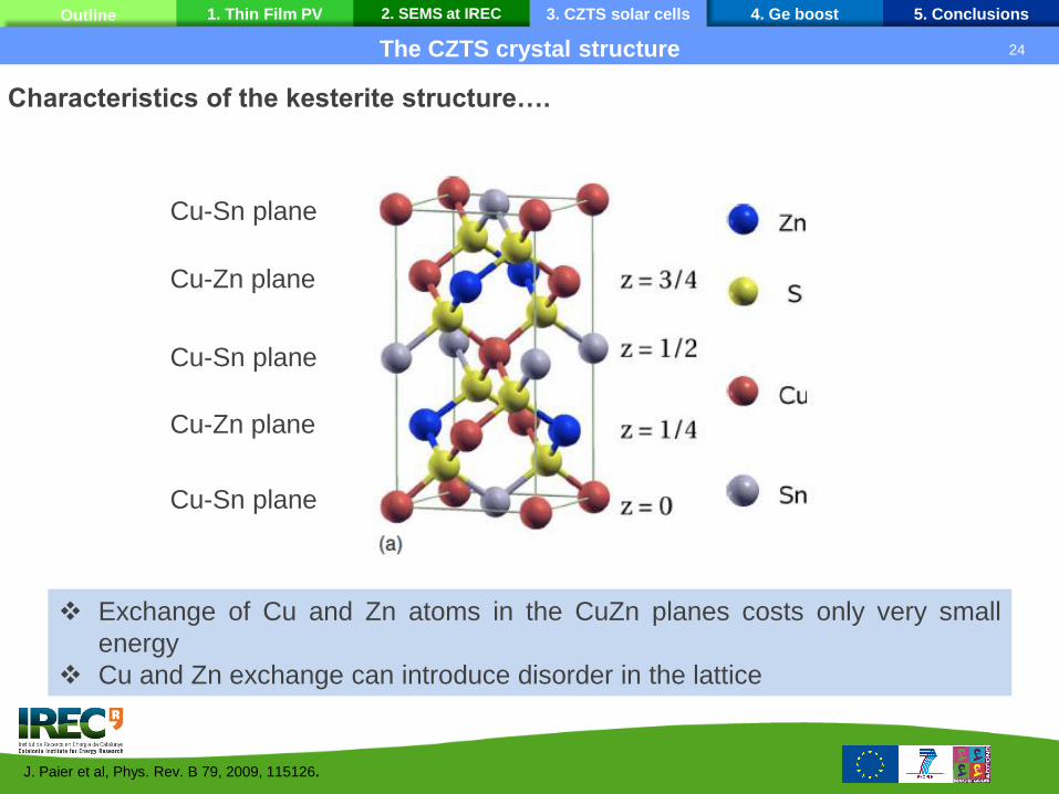
Characteristics of the kesterite structure….
J. Paier et al, Phys. Rev. B 79, 2009, 115126.
Cu-Sn plane
Cu-Sn plane
Cu-Zn plane
Cu-Zn plane
Cu-Sn plane
Exchange of Cu and Zn atoms in the CuZn planes costs only very small
energy
Cu and Zn exchange can introduce disorder in the lattice
The CZTS crystal structure 24
4. Ge boost 5. Conclusions Outline 1. Thin Film PV 2. SEMS at IREC 3. CZTS solar cells
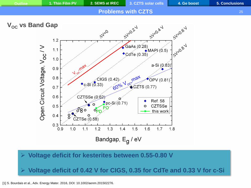
[1] S. Bourdais et al., Adv. Energy Mater. 2016, DOI: 10.1002/aenm.201502276.
Voltage deficit for kesterites between 0.55-0.80 V
Voltage deficit of 0.42 V for CIGS, 0.35 for CdTe and 0.33 V for c-Si
VOC vs Band Gap
Problems with CZTS 25
4. Ge boost 5. Conclusions Outline 1. Thin Film PV 2. SEMS at IREC 3. CZTS solar cells
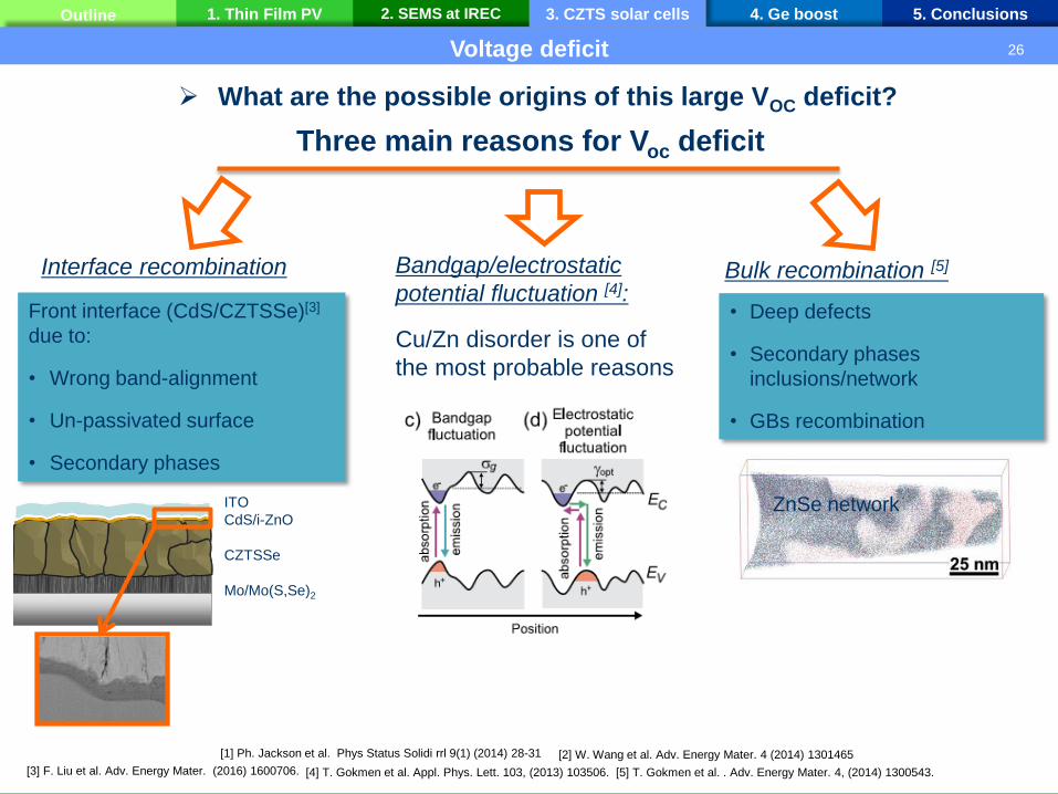
What are the possible origins of this large VOC deficit?
Interface recombination
Front interface (CdS/CZTSSe)[3]
due to:
• Wrong band-alignment
• Un-passivated surface
• Secondary phases
• Deep defects
• Secondary phases
inclusions/network
• GBs recombination
Bulk recombination [5] Bandgap/electrostatic
potential fluctuation [4]:
Cu/Zn disorder is one of
the most probable reasons
[1] Ph. Jackson et al. Phys Status Solidi rrl 9(1) (2014) 28-31 [2] W. Wang et al. Adv. Energy Mater. 4 (2014) 1301465
Three main reasons for Voc deficit
ITO
CdS/i-ZnO
CZTSSe
Mo/Mo(S,Se)2
[3] F. Liu et al. Adv. Energy Mater. (2016) 1600706. [4] T. Gokmen et al. Appl. Phys. Lett. 103, (2013) 103506. [5] T. Gokmen et al. . Adv. Energy Mater. 4, (2014) 1300543.
ZnSe network
Voltage deficit 26
4. Ge boost 5. Conclusions Outline 1. Thin Film PV 2. SEMS at IREC 3. CZTS solar cells
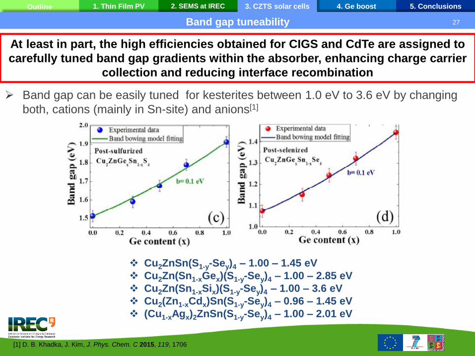
Cu2ZnSn(S1-y-Sey)4 – 1.00 – 1.45 eV
Cu2Zn(Sn1-xGex)(S1-y-Sey)4 – 1.00 – 2.85 eV
Cu2Zn(Sn1-xSix)(S1-y-Sey)4 – 1.00 – 3.6 eV
Cu2(Zn1-xCdx)Sn(S1-y-Sey)4 – 0.96 – 1.45 eV
(Cu1-xAgx)2ZnSn(S1-y-Sey)4 – 1.00 – 2.01 eV
Band gap can be easily tuned for kesterites between 1.0 eV to 3.6 eV by changing
both, cations (mainly in Sn-site) and anions[1]
Band gap tuneability
[1] D. B. Khadka, J. Kim, J. Phys. Chem. C 2015, 119, 1706
27
At least in part, the high efficiencies obtained for CIGS and CdTe are assigned to
carefully tuned band gap gradients within the absorber, enhancing charge carrier
collection and reducing interface recombination
5. Conclusions Outline 1. Thin Film PV 2. SEMS at IREC 3. CZTS solar cells 4. Ge boost
Ge boost
1. Thin Film Photovoltaics • PV Technologies(CIGS / CdTe/ a-Si) • Why Thin Film PV? • Technologies
2. The SEMS group at IREC • Presentation of the group and institute • Main research lines • Examples
3. The kesterite solar cell • Standard process and device architecture • The absorber material • Challenges
4. Ge boosting CZTS cell efficiencies • Experimental – Ge layer optimization • Growth model and impact on crystal grains/grain boundaries • Bifacial crystallisation
5. Conclusions
28
30
5. Conclusions Outline 1. Thin Film PV 2. SEMS at IREC 3. CZTS solar cells 4. Ge boost
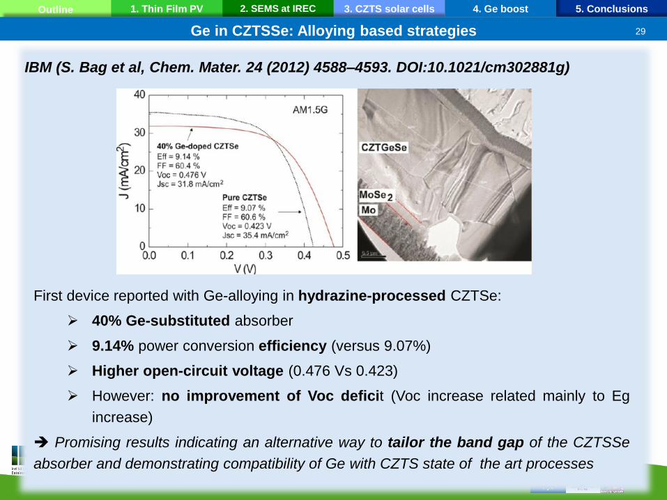
First device reported with Ge-alloying in hydrazine-processed CZTSe:
40% Ge-substituted absorber
9.14% power conversion efficiency (versus 9.07%)
Higher open-circuit voltage (0.476 Vs 0.423)
However: no improvement of Voc deficit (Voc increase related mainly to Eg
increase)
Promising results indicating an alternative way to tailor the band gap of the CZTSSe
absorber and demonstrating compatibility of Ge with CZTS state of the art processes
IBM (S. Bag et al, Chem. Mater. 24 (2012) 4588–4593. DOI:10.1021/cm302881g)
Ge in CZTSSe: Alloying based strategies
29
5. Conclusions Outline 1. Thin Film PV 2. SEMS at IREC 3. CZTS solar cells 4. Ge boost
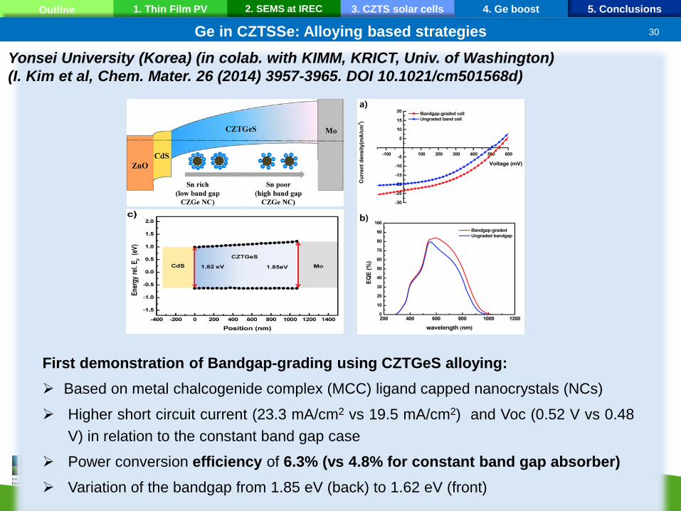
Yonsei University (Korea) (in colab. with KIMM, KRICT, Univ. of Washington)
(I. Kim et al, Chem. Mater. 26 (2014) 3957-3965. DOI 10.1021/cm501568d)
First demonstration of Bandgap-grading using CZTGeS alloying:
Based on metal chalcogenide complex (MCC) ligand capped nanocrystals (NCs)
Higher short circuit current (23.3 mA/cm2 vs 19.5 mA/cm2) and Voc (0.52 V vs 0.48
V) in relation to the constant band gap case
Power conversion efficiency of 6.3% (vs 4.8% for constant band gap absorber)
Variation of the bandgap from 1.85 eV (back) to 1.62 eV (front)
Ge in CZTSSe: Alloying based strategies
30
5. Conclusions Outline 1. Thin Film PV 2. SEMS at IREC 3. CZTS solar cells 4. Ge boost
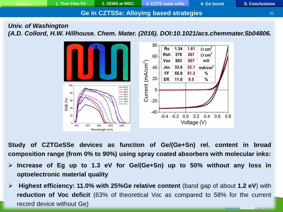
Study of CZTGeSSe devices as function of Ge/(Ge+Sn) rel. content in broad
composition range (from 0% to 90%) using spray coated absorbers with molecular inks:
Increase of Eg up to 1.3 eV for Ge/(Ge+Sn) up to 50% without any loss in
optoelectronic material quality
Highest efficiency: 11.0% with 25%Ge relative content (band gap of about 1.2 eV) with
reduction of Voc deficit (63% of theoretical Voc as compared to 58% for the current
record device without Ge)
Univ. of Washington
(A.D. Collord, H.W. Hillhouse. Chem. Mater. (2016). DOI:10.1021/acs.chemmater.5b04806.
Ge in CZTSSe: Alloying based strategies
31
5. Conclusions Outline 1. Thin Film PV 2. SEMS at IREC 3. CZTS solar cells 4. Ge boost
Increased VOC but in some cases linked to higher band-gap
Potential for graded band-gap concepts
Improvement of grain growth and crystallinity
Increased minority charge carrier lifetime
Large potential to reduce VOC deficit in current kesterite technology
INVOLVING RELATIVELY LARGE AMOUNT OF Ge (20-40% Ge-substitution)
Univ. of Washington
IREC Approach: deposition of a Ge nanolayer on top of the metallic
precursors, before selenisation.
In summary: Ge alloying has demonstrated…
[1] A.D. Collord, H.W. Hillhouse. Chem. Mater. (2016). DOI:10.1021/acs.chemmater.5b04806
32
5. Conclusions Outline 1. Thin Film PV 2. SEMS at IREC 3. CZTS solar cells 4. Ge boost
Cu/Sn/Cu/Zn
Ge nano-layer
SLG
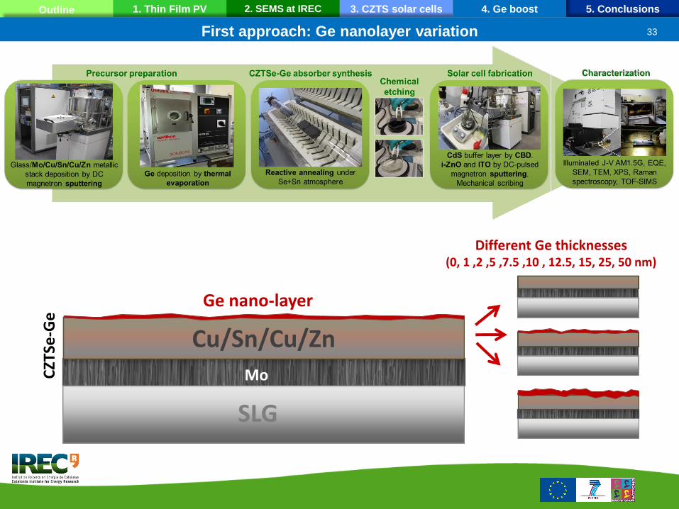
Different Ge thicknesses (0, 1 ,2 ,5 ,7.5 ,10 , 12.5, 15, 25, 50 nm)
Mo CZT
Se-G
e First approach: Ge nanolayer variation 33
5. Conclusions Outline 1. Thin Film PV 2. SEMS at IREC 3. CZTS solar cells 4. Ge boost
0 5 10 15 20 25380
400
420
440
460
Average
Best cell
VO
C (
mV
)
Ge thickness (nm)
453 mV
0 5 10 15 20 25
56
60
64
68
Ge thickness (nm)
Average
Best cell
FF
(%
)
66.8 %
0 5 10 15 20 25
28
30
32
34
Ge thickness (nm)
Average
Best cell
JS
C (
mA
/cm
2)
33.3 mA/cm2
0 10 20 30 40 505
6
7
8
9
10
11
Average
Best cell
Eff
icie
ncy (
%)
Ge thickness (nm)
10.1 % [1]
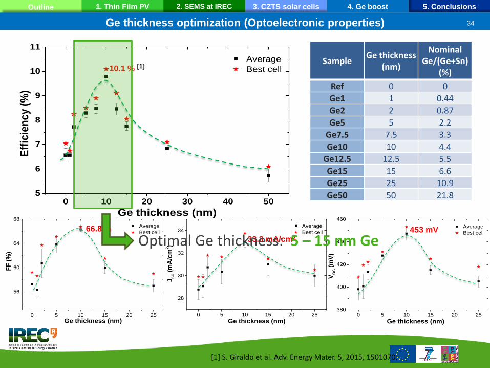
Optimal Ge thickness: 5 – 15 nm Ge
Sample Ge thickness
(nm)
Nominal Ge/(Ge+Sn)
(%)
Ref 0 0
Ge1 1 0.44
Ge2 2 0.87
Ge5 5 2.2
Ge7.5 7.5 3.3
Ge10 10 4.4
Ge12.5 12.5 5.5
Ge15 15 6.6
Ge25 25 10.9
Ge50 50 21.8
[1] S. Giraldo et al. Adv. Energy Mater. 5, 2015, 1501070.
Ge thickness optimization (Optoelectronic properties)
34
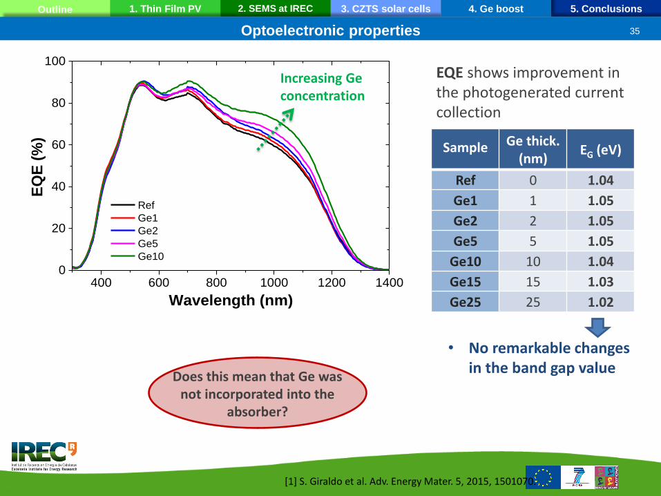
5. Conclusions Outline 1. Thin Film PV 2. SEMS at IREC 3. CZTS solar cells 4. Ge boost
400 600 800 1000 1200 14000
20
40
60
80
100
E
QE
(%
)
Wavelength (nm)
Ref
Ge1
Ge2
Ge5
Ge10
Increasing Ge concentration
EQE shows improvement in the photogenerated current collection
• No remarkable changes in the band gap value
Sample Ge thick.
(nm) EG (eV)
Ref 0 1.04
Ge1 1 1.05
Ge2 2 1.05
Ge5 5 1.05
Ge10 10 1.04
Ge15 15 1.03
Ge25 25 1.02
Does this mean that Ge was not incorporated into the
absorber?
[1] S. Giraldo et al. Adv. Energy Mater. 5, 2015, 1501070.
Optoelectronic properties
35
5. Conclusions Outline 1. Thin Film PV 2. SEMS at IREC 3. CZTS solar cells 4. Ge boost
1. Where is Ge located?
2. Why can such low amount of Ge lead to
this large efficiency improvement?
[1] S. Giraldo et al. Adv. Energy Mater. 5, 2015, 1501070.
Optoelectronic properties
Finding Germanium…
36
5. Conclusions Outline 1. Thin Film PV 2. SEMS at IREC 3. CZTS solar cells 4. Ge boost
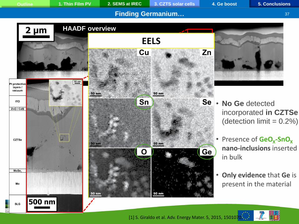
HAADF overview
EELS
• No Ge detected
incorporated in CZTSe
(detection limit = 0.2%)
• Presence of GeOX-SnOX nano-inclusions inserted in bulk
• Only evidence that Ge is
present in the material
[1] S. Giraldo et al. Adv. Energy Mater. 5, 2015, 1501070.
Finding Germanium… 37
5. Conclusions Outline 1. Thin Film PV 2. SEMS at IREC 3. CZTS solar cells 4. Ge boost
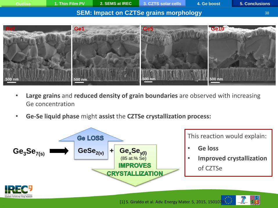
• Large grains and reduced density of grain boundaries are observed with increasing Ge concentration
500 nm 500 nm 500 nm 500 nm
Ref Ge1 Ge5 Ge10
Ge3Se7(s) GeSe2(v) + GexSey(l)
(85 at.% Se)
• Ge-Se liquid phase might assist the CZTSe crystallization process:
This reaction would explain:
• Ge loss
• Improved crystallization
of CZTSe
[1] S. Giraldo et al. Adv. Energy Mater. 5, 2015, 1501070.
SEM: Impact on CZTSe grains morphology
38
5. Conclusions Outline 1. Thin Film PV 2. SEMS at IREC 3. CZTS solar cells 4. Ge boost
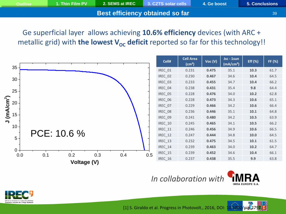
Ge superficial layer allows achieving 10.6% efficiency devices (with ARC + metallic grid) with the lowest VOC deficit reported so far for this technology!!
In collaboration with
Cell# Cell Area
(cm²) Voc (V)
Jsc - 1sun
(mA/cm²) Eff (%) FF (%)
IREC_01 0.231 0.475 35.1 10.3 61.7
IREC_02 0.230 0.467 34.6 10.4 64.5
IREC_03 0.233 0.455 34.7 10.4 66.2
IREC_04 0.238 0.431 35.4 9.8 64.4
IREC_05 0.228 0.476 34.0 10.2 62.8
IREC_06 0.228 0.473 34.3 10.6 65.1
IREC_07 0.229 0.466 34.2 10.6 66.4
IREC_08 0.236 0.446 35.1 10.1 64.8
IREC_09 0.241 0.480 34.2 10.5 63.9
IREC_10 0.245 0.465 34.1 10.5 66.2
IREC_11 0.246 0.456 34.9 10.6 66.5
IREC_12 0.247 0.444 34.8 10.0 64.5
IREC_13 0.232 0.475 34.5 10.1 61.5
IREC_14 0.239 0.463 34.0 10.2 64.7
IREC_15 0.239 0.452 34.6 10.4 66.1
IREC_16 0.237 0.438 35.5 9.9 63.8 0.0 0.1 0.2 0.3 0.4 0.5
0
5
10
15
20
25
30
35
J (
mA
/cm
2)
Voltage (V)
[1] S. Giraldo et al. Progress in Photovolt., 2016, DOI: 10.1002/pip.2797.
PCE: 10.6 %
39 Best efficiency obtained so far
5. Conclusions Outline 1. Thin Film PV 2. SEMS at IREC 3. CZTS solar cells 4. Ge boost
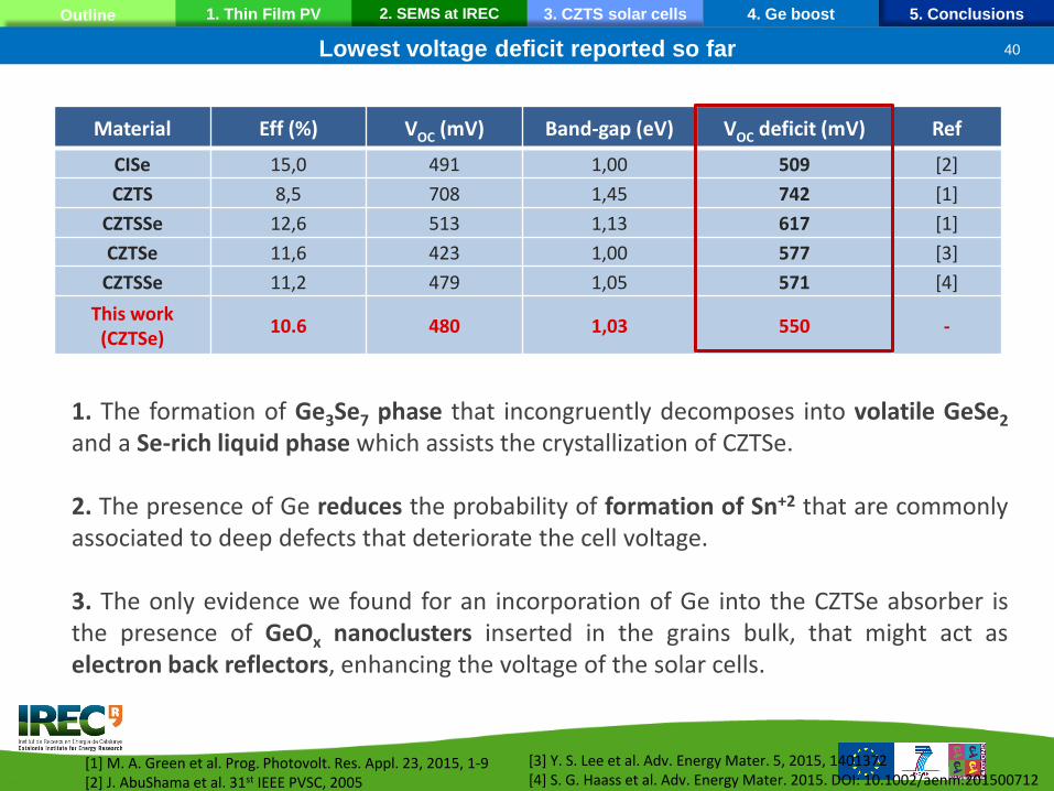
Material Eff (%) VOC (mV) Band-gap (eV) VOC deficit (mV) Ref
CISe 15,0 491 1,00 509 [2]
CZTS 8,5 708 1,45 742 [1]
CZTSSe 12,6 513 1,13 617 [1]
CZTSe 11,6 423 1,00 577 [3]
CZTSSe 11,2 479 1,05 571 [4]
This work (CZTSe)
10.6 480 1,03 550 -
1. The formation of Ge3Se7 phase that incongruently decomposes into volatile GeSe2 and a Se-rich liquid phase which assists the crystallization of CZTSe. 2. The presence of Ge reduces the probability of formation of Sn+2 that are commonly associated to deep defects that deteriorate the cell voltage. 3. The only evidence we found for an incorporation of Ge into the CZTSe absorber is the presence of GeOx nanoclusters inserted in the grains bulk, that might act as electron back reflectors, enhancing the voltage of the solar cells.
[3] Y. S. Lee et al. Adv. Energy Mater. 5, 2015, 1401372 [4] S. G. Haass et al. Adv. Energy Mater. 2015. DOI: 10.1002/aenm.201500712
[1] M. A. Green et al. Prog. Photovolt. Res. Appl. 23, 2015, 1-9 [2] J. AbuShama et al. 31st IEEE PVSC, 2005
Lowest voltage deficit reported so far 40
5. Conclusions Outline 1. Thin Film PV 2. SEMS at IREC 3. CZTS solar cells 4. Ge boost
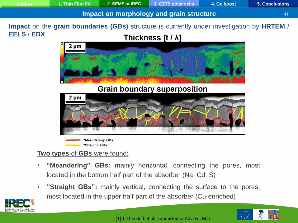
Impact on the grain boundaries (GBs) structure is currently under investigation by HRTEM /
EELS / EDX
Two types of GBs were found:
• “Meandering” GBs: mainly horizontal, connecting the pores, most
located in the bottom half part of the absorber (Na, Cd, S)
• “Straight GBs”: mainly vertical, connecting the surface to the pores,
most located in the upper half part of the absorber (Cu-enriched)
“Meandering” GBs
“Straight” GBs
[1] T. Thersleff et al., submitted to Adv. En. Mat.
Impact on morphology and grain structure 41
5. Conclusions Outline 1. Thin Film PV 2. SEMS at IREC 3. CZTS solar cells 4. Ge boost
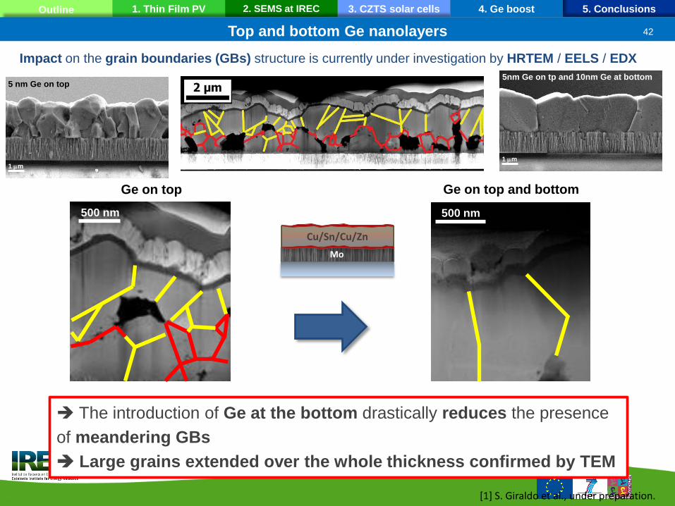
The introduction of Ge at the bottom drastically reduces the presence
of meandering GBs
Large grains extended over the whole thickness confirmed by TEM
500 nm
Ge on top and bottom
500 nm
Ge on top
Impact on the grain boundaries (GBs) structure is currently under investigation by HRTEM / EELS / EDX
[1] S. Giraldo et al., under preparation.
1 m
5nm Ge on tp and 10nm Ge at bottom
1 m
5 nm Ge on top
Top and bottom Ge nanolayers
Cu/Sn/Cu/Zn
Mo
42
5. Conclusions Outline 1. Thin Film PV 2. SEMS at IREC 3. CZTS solar cells 4. Ge boost
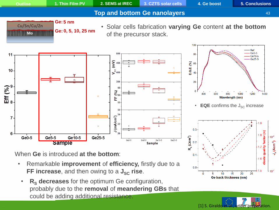
When Ge is introduced at the bottom:
• Remarkable improvement of efficiency, firstly due to a
FF increase, and then owing to a JSC rise.
• RS decreases for the optimum Ge configuration,
probably due to the removal of meandering GBs that
could be adding additional resistance.
Cu/Sn/Cu/Zn
Mo
Ge:
Ge: 0, 5, 10, 25 nm
5 nm • Solar cells fabrication varying Ge content at the bottom
of the precursor stack.
• EQE confirms the JSC increase
[1] S. Giraldo et al., under preparation.
Top and bottom Ge nanolayers 43
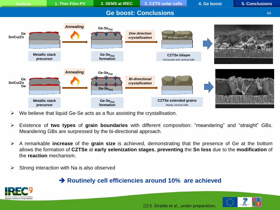
5. Conclusions Outline 1. Thin Film PV 2. SEMS at IREC 3. CZTS solar cells 4. Ge boost
Annealing
Ge Sn/Cu/Zn
Ge-Se(liq)
One direction
crystallization
Metallic stack
precursor
Ge-Se(liq)
formation
CZTSe bilayer
Horizontal and vertical GBs
Annealing
Ge Sn/Cu/Zn
Ge-Se(liq)
Bi-directional crystallization
Metallic stack
precursor
Ge-Se(liq)
formation
CZTSe extended grains
Mainly vertical GBs
Ge Ge-Se(liq)
Routinely cell efficiencies around 10% are achieved
We believe that liquid Ge-Se acts as a flux assisting the crystallisation.
Existence of two types of grain boundaries with different composition: “meandering” and “straight” GBs.
Meandering GBs are surpressed by the bi-directional approach.
A remarkable increase of the grain size is achieved, demonstrating that the presence of Ge at the bottom
allows the formation of CZTSe at early selenization stages, preventing the Sn loss due to the modification of
the reaction mechanism.
Strong interaction with Na is also observed
[1] S. Giraldo et al., under preparation.
Ge boost: Conclusions 44
Outline 1. Thin Film PV 2. SEMS at IREC 3. CZTS solar cells 4. Ge boost 5. Conclusions
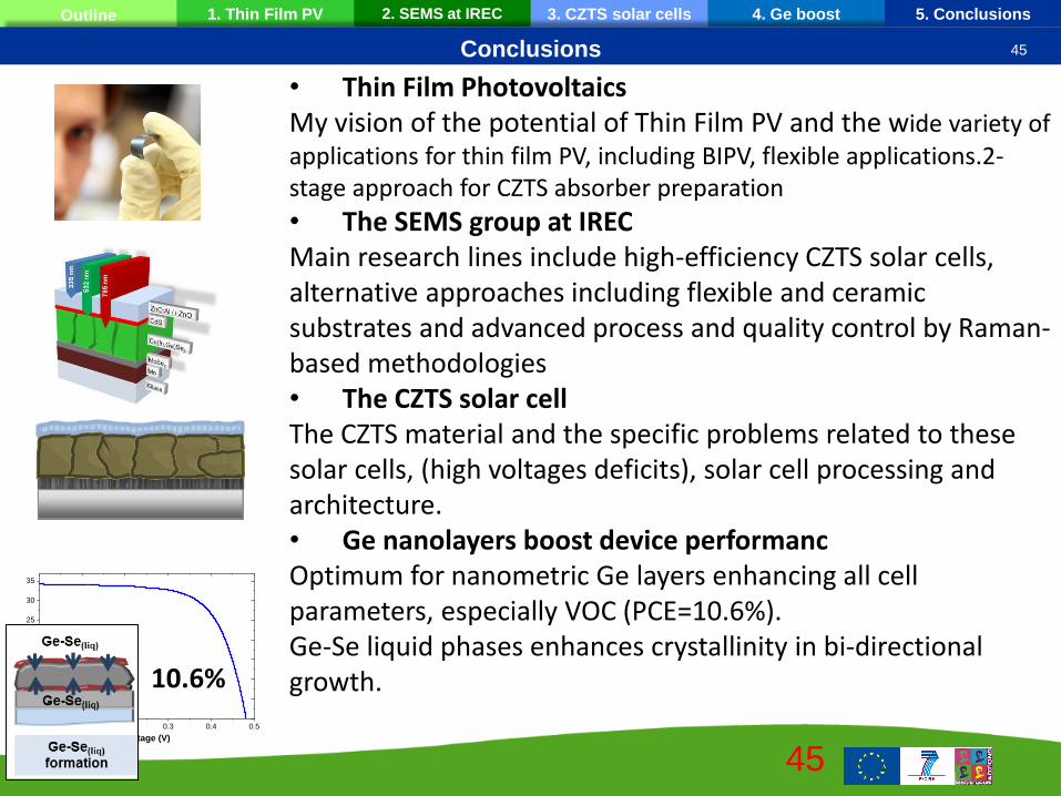
Conclusions
• Thin Film Photovoltaics My vision of the potential of Thin Film PV and the wide variety of applications for thin film PV, including BIPV, flexible applications.2-stage approach for CZTS absorber preparation
• The SEMS group at IREC Main research lines include high-efficiency CZTS solar cells, alternative approaches including flexible and ceramic substrates and advanced process and quality control by Raman-based methodologies • The CZTS solar cell The CZTS material and the specific problems related to these solar cells, (high voltages deficits), solar cell processing and architecture. • Ge nanolayers boost device performanc Optimum for nanometric Ge layers enhancing all cell parameters, especially VOC (PCE=10.6%). Ge-Se liquid phases enhances crystallinity in bi-directional growth.
u/Zn Ge
0.0 0.1 0.2 0.3 0.4 0.50
5
10
15
20
25
30
35
J (
mA
/cm
2)
Voltage (V)
10.6%
45
45
IREC – Solar Energy Materials and System Group: Prof. Alejandro Pérez-Rodríguez
SEMS Lab: Edgardo Saucedo, Paul Pistor, Marcel Placidi, Moises Espindola, Sergio Giraldo, Haibing Xie, Diouldé Sylla, Ignacio Becerril, Markus Neuschitzer
Former members: Monica Colina, Simon López-Mariño (Crystalsol)
Raman workshop: Victor Izquierdo-Roca, Florian Oliva, Max Guc, Laia Arquès
Former members: Mirjana Dimitrievska , Andrew Fairbrother (NREL-NIST)
University of Barcelona: Lorenzo Calvo-Barrio, Tariq Jawhari, Xavier Alcobé
Ångström Laboratory, Uppsala University: Klaus Leiffer, Thomas Thersleff
IMRA: Gilles Denler, Gerardo Larramona
Acknowledgements
Funding from the European
Union’s Seventh
Framework Programme
under reference number
FP7-PEOPLE-2013-IEF-
625840 (“JumpKEST”) is
gratefully acknowledged
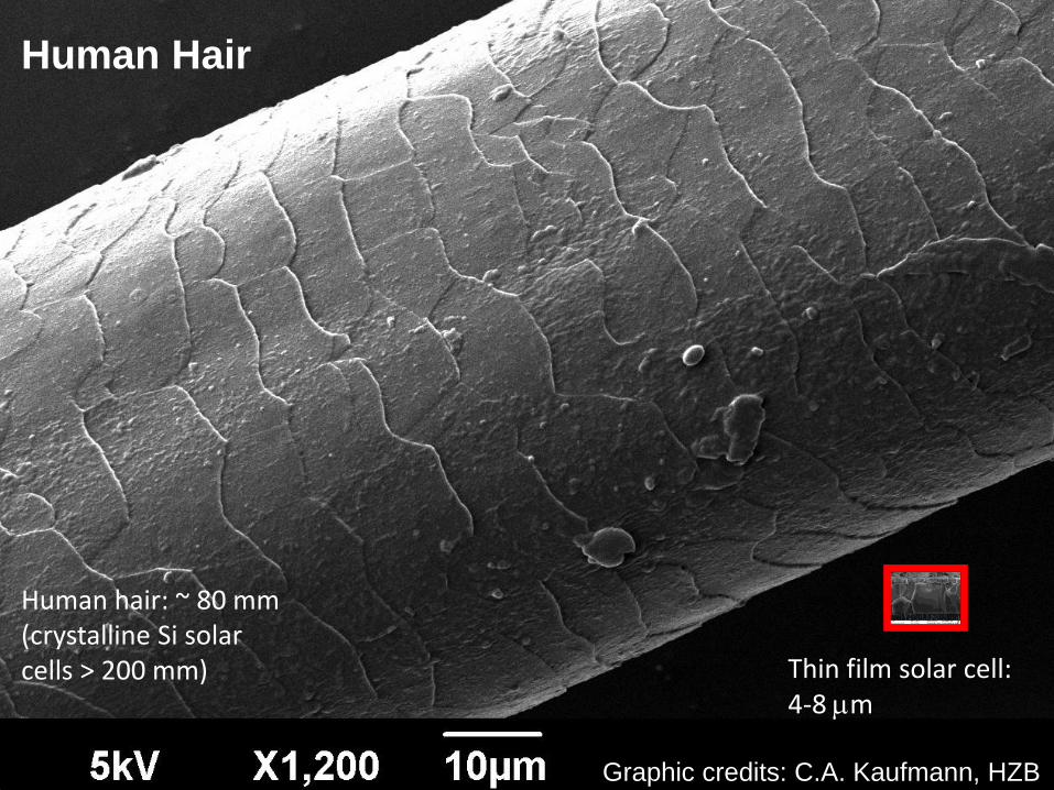
Thin film solar cell:
~ 4-8 m
47
Human Hair
Human hair: ~ 80 mm (crystalline Si solar cells > 200 mm) Thin film solar cell:
4-8 m
Graphic credits: C.A. Kaufmann, HZB
3. Ge boost 4. Alt. Approaches 5. Conclusions Outline 1. Thin Film PV 2. CZTS solar cells
Crystal structure of CZTS 48
48
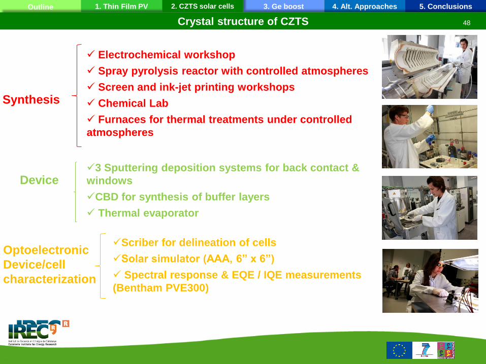
Electrochemical workshop
Spray pyrolysis reactor with controlled atmospheres
Screen and ink-jet printing workshops
Chemical Lab
Furnaces for thermal treatments under controlled
atmospheres
Synthesis
Device
Optoelectronic
Device/cell
characterization
3 Sputtering deposition systems for back contact &
windows
CBD for synthesis of buffer layers
Thermal evaporator
Scriber for delineation of cells
Solar simulator (AAA, 6” x 6”)
Spectral response & EQE / IQE measurements
(Bentham PVE300)
3. Ge boost 4. Alt. Approaches 5. Conclusions Outline 1. Thin Film PV 2. CZTS solar cells
49
Characterisation Infrastructure 49
49
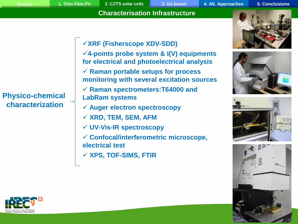
XRF (Fisherscope XDV-SDD)
4-points probe system & I(V) equipments
for electrical and photoelectrical analysis
Raman portable setups for process
monitoring with several excitation sources
Raman spectrometers:T64000 and
LabRam systems
Auger electron spectroscopy
XRD, TEM, SEM, AFM
UV-Vis-IR spectroscopy
Confocal/interferometric microscope,
electrical test
XPS, TOF-SIMS, FTIR
Physico-chemical
characterization
3. Ge boost 4. Alt. Approaches 5. Conclusions Outline 1. Thin Film PV 2. CZTS solar cells
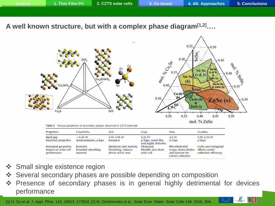
Cu-Sn plane
Cu-Sn plane
Cu-Zn plane
Cu-Zn plane
Cu-Sn plane
A well known structure, but with a complex phase diagram[1,2]….
[1] H. Du et al. J. Appl. Phys. 115, 20015, 173502, [2] M. Dimitrievska et al., Solar Ener. Mater. Solar Cells 149, 2016, 304,
Small single existence region
Several secondary phases are possible depending on composition
Presence of secondary phases is in general highly detrimental for devices
performance
3. Ge boost 4. Alt. Approaches 5. Conclusions Outline 1. Thin Film PV 2. CZTS solar cells
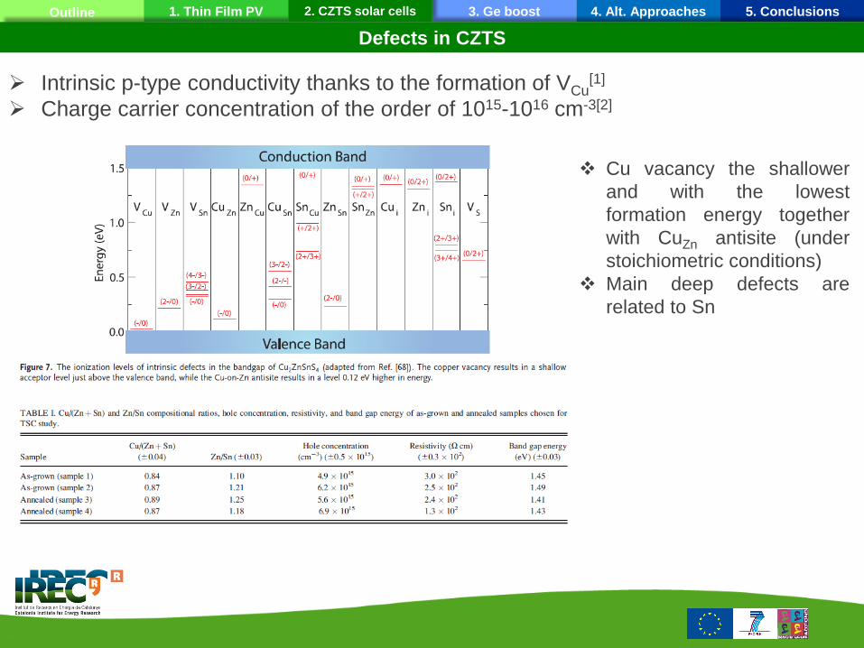
Cu vacancy the shallower
and with the lowest
formation energy together
with CuZn antisite (under
stoichiometric conditions)
Main deep defects are
related to Sn
Intrinsic p-type conductivity thanks to the formation of VCu[1]
Charge carrier concentration of the order of 1015-1016 cm-3[2]
Defects in CZTS
Purdue Univ. (in collab. with HZB and Cottbus Univ.)
C.J. Hages et al, Prog. Photovoltaics Res. Appl. 23 (2015) 376–384. DOI:10.1002/pip.2442.
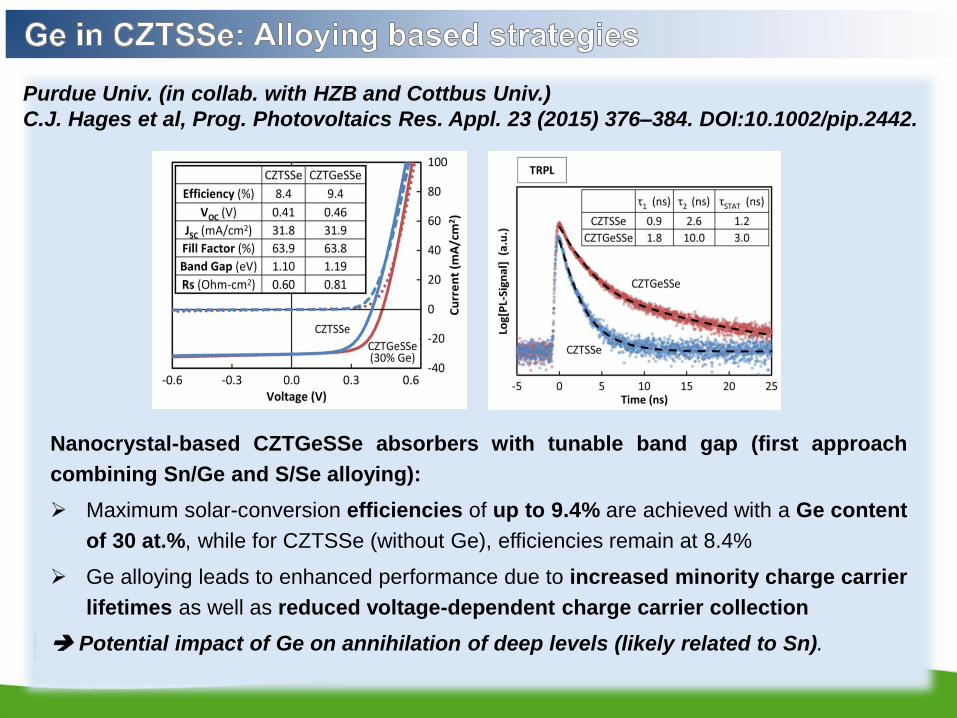
Nanocrystal-based CZTGeSSe absorbers with tunable band gap (first approach
combining Sn/Ge and S/Se alloying):
Maximum solar-conversion efficiencies of up to 9.4% are achieved with a Ge content
of 30 at.%, while for CZTSSe (without Ge), efficiencies remain at 8.4%
Ge alloying leads to enhanced performance due to increased minority charge carrier
lifetimes as well as reduced voltage-dependent charge carrier collection
Potential impact of Ge on annihilation of deep levels (likely related to Sn).
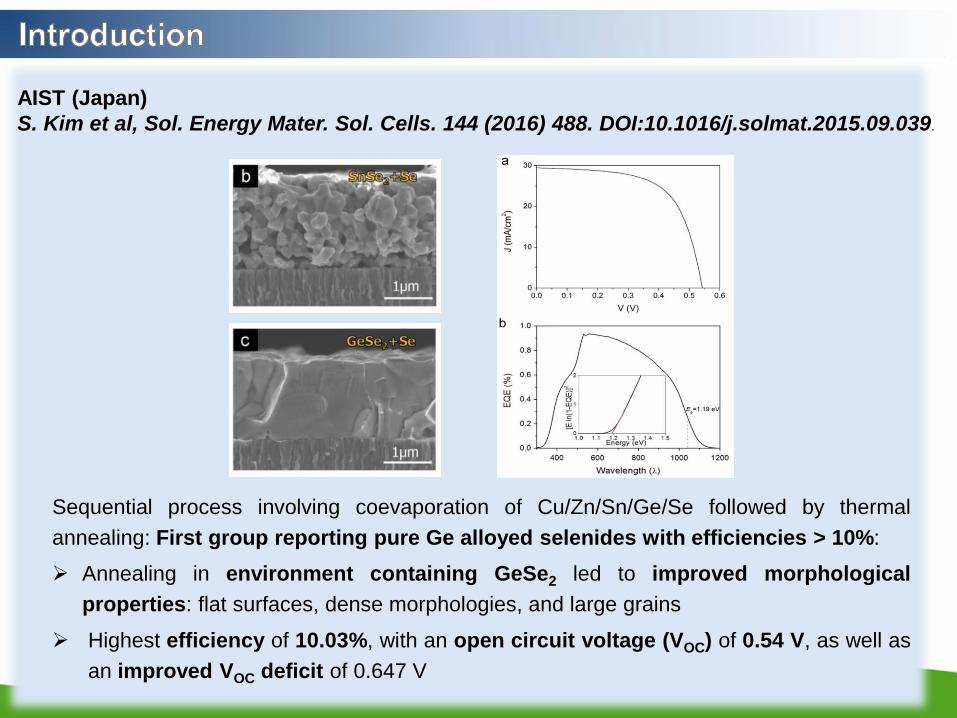
Sequential process involving coevaporation of Cu/Zn/Sn/Ge/Se followed by thermal
annealing: First group reporting pure Ge alloyed selenides with efficiencies > 10%:
Annealing in environment containing GeSe2 led to improved morphological
properties: flat surfaces, dense morphologies, and large grains
Highest efficiency of 10.03%, with an open circuit voltage (VOC) of 0.54 V, as well as
an improved VOC deficit of 0.647 V
AIST (Japan)
S. Kim et al, Sol. Energy Mater. Sol. Cells. 144 (2016) 488. DOI:10.1016/j.solmat.2015.09.039.

0 10 20 30 40 50 60 700
100
200
300
400
500
600
700
T (
ºC)
time (min)
1 m
Ge10
1 m
Ge10
1 m
5nm Ge on tp and 10nm Ge at bottom
Ref
1 m
Ge25
1 m
1 m
5 nm Ge on top
• Experiment stopping the annealing process at different points
1 m
Ge10
• Uniform microcrystalline kesterite
• By using Ge at the bottom large crystals start to be observed at early selenization stages
´.
• Fast formation of well-
crystallized CZTSe with
large grains
• At the end of the
complete selenization
process, big crystals
extend over the whole
thickness
[1] S. Giraldo et al., under preparation.
![432 IEEE JOURNAL OF PHOTOVOLTAICS, VOL. 4, NO. 1, … · B. Flexible Thin-Film Batteries Commercial flexible thin-film lithium-ion (Li-ion) batter-ies [4] are used for energy storage.](https://static.fdocuments.in/doc/165x107/5f7c3a746e72e23f55360f11/432-ieee-journal-of-photovoltaics-vol-4-no-1-b-flexible-thin-film-batteries.jpg)