
Thermomechanical Failure Analysis of Through-Silicon …ruihuang/papers/IEEE_TDMR2013.pdf ·...
9
318 IEEE TRANSACTIONS ON DEVICE AND MATERIALS RELIABILITY, VOL. 14, NO. 1, MARCH 2014 Thermomechanical Failure Analysis of Through-Silicon Via Interface Using a Shear-Lag Model With Cohesive Zone Suk-Kyu Ryu, Tengfei Jiang, Jay Im, Paul S. Ho, Fellow, IEEE, and Rui Huang Abstract—An analytical approach to predict initiation and growth of interfacial delamination in the through-silicon via struc- ture is developed by combining a cohesive zone model with a shear-lag model. Two critical temperatures are predicted for dam- age initiation and fracture initiation, respectively. It is found that via extrusion significantly increases beyond the second critical temperature. The dependence of the critical temperatures on the material/interfacial properties, as well as the via size (diameter and height), is discussed. In parallel with the analytical approach, finite-element models with cohesive interface elements are em- ployed to numerically simulate the initiation and the progression of interfacial delamination. The numerical results are in good agreement with the analytical solution, and both are qualitatively consistent with reported experimental findings by others. Index Terms—Cohesive zone model (CZM), finite-element analysis (FEA), interfacial reliability, shear-lag model, thermal stresses, thermomechanical, through-silicon via (TSV). I. I NTRODUCTION T HREE-DIMENSIONAL (3-D) integration has emerged as an effective approach to overcome the wiring limit im- posed on chip performance, density and power consumption be- yond the current technology node [1]–[6]. Through-silicon vias (TSVs) are important elements for 3-D integration providing direct die-to-die connections to form stacked structures. While the 3-D integration with TSVs offers a promising solution for future technology nodes, serious thermomechanical reliability concerns have been raised [7]–[16]. Due to the coefficient of thermal expansion (CTE) mismatch between the via materials and Si, thermal stresses are ubiquitously induced during pro- cessing and thermal cycling of the TSV structures. In some cases, the induced thermal stress is sufficiently high to cause cracking or interfacial delamination of the integrated TSV structures [7]–[10]. In some other cases, the stresses around TSVs may affect the carrier mobility due to the piezoresistivity effect, leading to spatial variation in performance for nearby electronic devices [11]–[13]. Moreover, extrusion of Cu vias Manuscript received January 16, 2013; revised March 20, 2013; accepted April 15, 2013. Date of publication May 2, 2013; date of current version March 4, 2014. This work was supported by the Semiconductor Research Corporation. S.-K. Ryu and R. Huang are with the Department of Aerospace Engineering and Engineering Mechanics, University of Texas, Austin, TX 78712 USA (e-mail: [email protected]). T. Jiang, J. Im, and P. S. Ho are with the Microelectronics Research Center, University of Texas, Austin, TX 78712 USA (e-mail: [email protected]). Color versions of one or more of the figures in this paper are available online at http://ieeexplore.ieee.org. Digital Object Identifier 10.1109/TDMR.2013.2261300 Fig. 1. Observations of via extrusion and interfacial delamination in TSV structures: (a) Via extrusion after thermal cycling [14]; (b) and (c) Interfacial delamination due to via extrusion [16]. out of Si surface is frequently observed in the TSV structures undergoing high temperature excursion [14]–[17] as shown in Fig. 1. The via extrusion can cause interfacial failure of a TSV and/or cracking in Si near the lower end of TSVs during the thermal processing [16]. To assess the interfacial reliability of TSV structures, we present an analytical approach, which combines a cohesive zone model with a shear-lag model to describe the debonding process. The via extrusion is predicted as a function of the temperature and compared with experimental data. Two critical temperatures are identified from the analytical solution and are compared with finite-element analysis. II. COHESIVE ZONE MODEL (CZM) Cohesive zone models (CZMs) have been widely employed to study the failure processes including nucleation and growth of interfacial cracks [18]–[25]. In the CZM approach, the constitutive behavior of an interface is described by a nonlinear traction-separation law. Various forms of the traction-separation law have been used, such as the perfect plasticity model [22], smooth nonlinear model [23], trapezoidal model [24], and bi- linear or triangular model [25]. In the present study, the bilinear traction-separation law (Fig. 2) is employed. During via extrusion, the interfacial failure is primarily in mode II (shearing mode) [7]. The shear traction at the interface is related to the sliding displacement along the tangential di- rection by the traction-separation law. Starting from an intact interface, the shear traction first increases linearly with the sliding displacement, with an initial stiffness K 0 . At a critical displacement, the shear traction reaches its maximum, τ max , after which the shear traction decreases with further sliding due to damage accumulation at the interface. Eventually, the 1530-4388 © 2013 IEEE. Personal use is permitted, but republication/redistribution requires IEEE permission. See http://www.ieee.org/publications_standards/publications/rights/index.html for more information.
Transcript of Thermomechanical Failure Analysis of Through-Silicon …ruihuang/papers/IEEE_TDMR2013.pdf ·...

318 IEEE TRANSACTIONS ON DEVICE AND MATERIALS RELIABILITY, VOL. 14, NO. 1, MARCH 2014
Thermomechanical Failure Analysis ofThrough-Silicon Via Interface Using a Shear-Lag
Model With Cohesive ZoneSuk-Kyu Ryu, Tengfei Jiang, Jay Im, Paul S. Ho, Fellow, IEEE, and Rui Huang
Abstract—An analytical approach to predict initiation andgrowth of interfacial delamination in the through-silicon via struc-ture is developed by combining a cohesive zone model with ashear-lag model. Two critical temperatures are predicted for dam-age initiation and fracture initiation, respectively. It is found thatvia extrusion significantly increases beyond the second criticaltemperature. The dependence of the critical temperatures on thematerial/interfacial properties, as well as the via size (diameterand height), is discussed. In parallel with the analytical approach,finite-element models with cohesive interface elements are em-ployed to numerically simulate the initiation and the progressionof interfacial delamination. The numerical results are in goodagreement with the analytical solution, and both are qualitativelyconsistent with reported experimental findings by others.
Index Terms—Cohesive zone model (CZM), finite-elementanalysis (FEA), interfacial reliability, shear-lag model, thermalstresses, thermomechanical, through-silicon via (TSV).
I. INTRODUCTION
THREE-DIMENSIONAL (3-D) integration has emerged asan effective approach to overcome the wiring limit im-
posed on chip performance, density and power consumption be-yond the current technology node [1]–[6]. Through-silicon vias(TSVs) are important elements for 3-D integration providingdirect die-to-die connections to form stacked structures. Whilethe 3-D integration with TSVs offers a promising solution forfuture technology nodes, serious thermomechanical reliabilityconcerns have been raised [7]–[16]. Due to the coefficient ofthermal expansion (CTE) mismatch between the via materialsand Si, thermal stresses are ubiquitously induced during pro-cessing and thermal cycling of the TSV structures. In somecases, the induced thermal stress is sufficiently high to causecracking or interfacial delamination of the integrated TSVstructures [7]–[10]. In some other cases, the stresses aroundTSVs may affect the carrier mobility due to the piezoresistivityeffect, leading to spatial variation in performance for nearbyelectronic devices [11]–[13]. Moreover, extrusion of Cu vias
Manuscript received January 16, 2013; revised March 20, 2013; acceptedApril 15, 2013. Date of publication May 2, 2013; date of current versionMarch 4, 2014. This work was supported by the Semiconductor ResearchCorporation.
S.-K. Ryu and R. Huang are with the Department of Aerospace Engineeringand Engineering Mechanics, University of Texas, Austin, TX 78712 USA(e-mail: [email protected]).
T. Jiang, J. Im, and P. S. Ho are with the Microelectronics Research Center,University of Texas, Austin, TX 78712 USA (e-mail: [email protected]).
Color versions of one or more of the figures in this paper are available onlineat http://ieeexplore.ieee.org.
Digital Object Identifier 10.1109/TDMR.2013.2261300
Fig. 1. Observations of via extrusion and interfacial delamination in TSVstructures: (a) Via extrusion after thermal cycling [14]; (b) and (c) Interfacialdelamination due to via extrusion [16].
out of Si surface is frequently observed in the TSV structuresundergoing high temperature excursion [14]–[17] as shown inFig. 1. The via extrusion can cause interfacial failure of a TSVand/or cracking in Si near the lower end of TSVs during thethermal processing [16].
To assess the interfacial reliability of TSV structures, wepresent an analytical approach, which combines a cohesivezone model with a shear-lag model to describe the debondingprocess. The via extrusion is predicted as a function of thetemperature and compared with experimental data. Two criticaltemperatures are identified from the analytical solution and arecompared with finite-element analysis.
II. COHESIVE ZONE MODEL (CZM)
Cohesive zone models (CZMs) have been widely employedto study the failure processes including nucleation and growthof interfacial cracks [18]–[25]. In the CZM approach, theconstitutive behavior of an interface is described by a nonlineartraction-separation law. Various forms of the traction-separationlaw have been used, such as the perfect plasticity model [22],smooth nonlinear model [23], trapezoidal model [24], and bi-linear or triangular model [25]. In the present study, the bilineartraction-separation law (Fig. 2) is employed.
During via extrusion, the interfacial failure is primarily inmode II (shearing mode) [7]. The shear traction at the interfaceis related to the sliding displacement along the tangential di-rection by the traction-separation law. Starting from an intactinterface, the shear traction first increases linearly with thesliding displacement, with an initial stiffness K0. At a criticaldisplacement, the shear traction reaches its maximum, τmax,after which the shear traction decreases with further slidingdue to damage accumulation at the interface. Eventually, the
1530-4388 © 2013 IEEE. Personal use is permitted, but republication/redistribution requires IEEE permission.See http://www.ieee.org/publications_standards/publications/rights/index.html for more information.
RYU et al.: THERMOMECHANICAL FAILURE ANALYSIS OF THROUGH-SILICON VIA INTERFACE 319
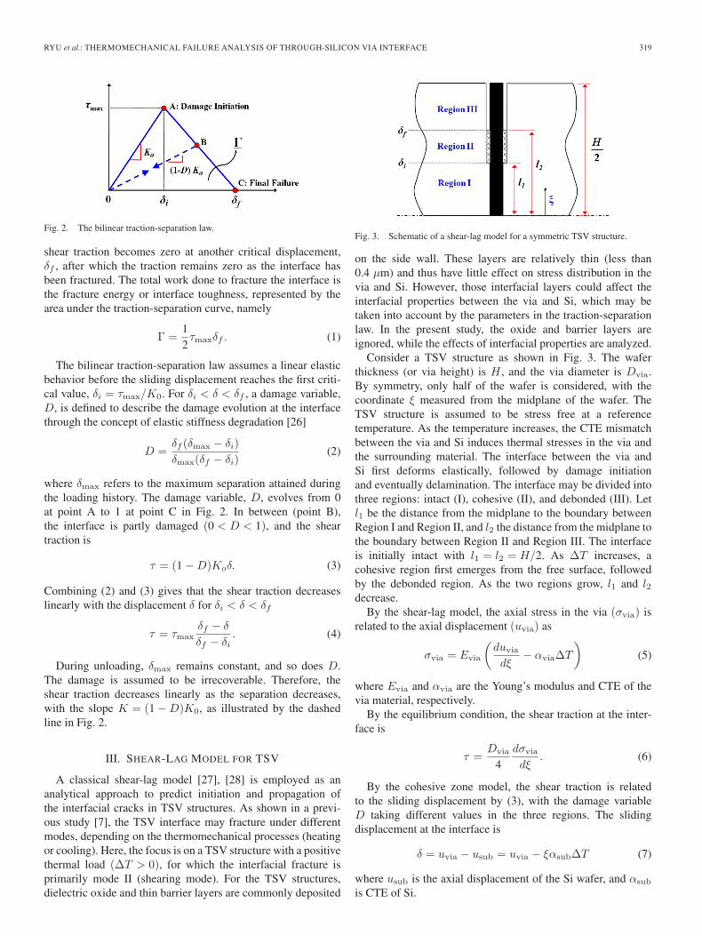
Fig. 2. The bilinear traction-separation law.
shear traction becomes zero at another critical displacement,δf , after which the traction remains zero as the interface hasbeen fractured. The total work done to fracture the interface isthe fracture energy or interface toughness, represented by thearea under the traction-separation curve, namely
Γ =12τmaxδf . (1)
The bilinear traction-separation law assumes a linear elasticbehavior before the sliding displacement reaches the first criti-cal value, δi = τmax/K0. For δi < δ < δf , a damage variable,D, is defined to describe the damage evolution at the interfacethrough the concept of elastic stiffness degradation [26]
D =δf (δmax − δi)
δmax(δf − δi)(2)
where δmax refers to the maximum separation attained duringthe loading history. The damage variable, D, evolves from 0at point A to 1 at point C in Fig. 2. In between (point B),the interface is partly damaged (0 < D < 1), and the sheartraction is
τ = (1 −D)Koδ. (3)
Combining (2) and (3) gives that the shear traction decreaseslinearly with the displacement δ for δi < δ < δf
τ = τmaxδf − δ
δf − δi. (4)
During unloading, δmax remains constant, and so does D.The damage is assumed to be irrecoverable. Therefore, theshear traction decreases linearly as the separation decreases,with the slope K = (1 −D)K0, as illustrated by the dashedline in Fig. 2.
III. SHEAR-LAG MODEL FOR TSV
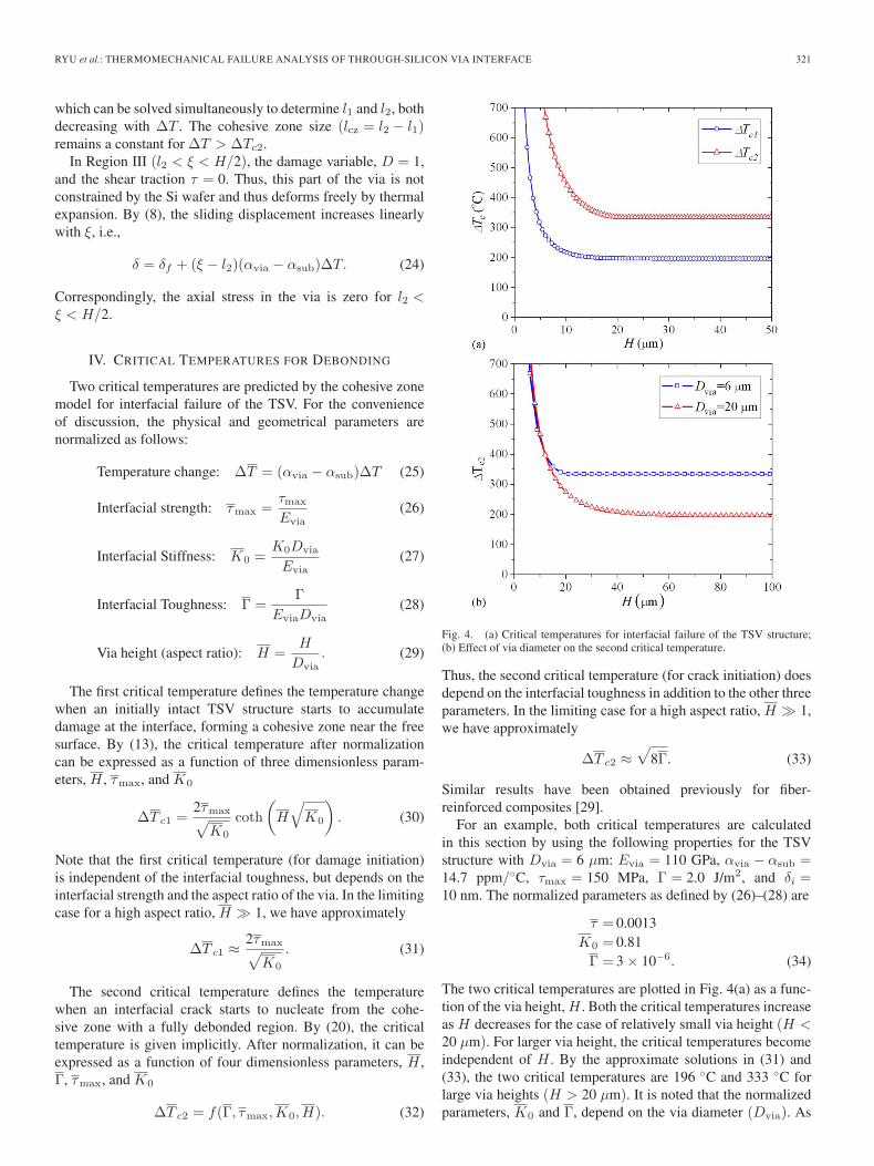
A classical shear-lag model [27], [28] is employed as ananalytical approach to predict initiation and propagation ofthe interfacial cracks in TSV structures. As shown in a previ-ous study [7], the TSV interface may fracture under differentmodes, depending on the thermomechanical processes (heatingor cooling). Here, the focus is on a TSV structure with a positivethermal load (ΔT > 0), for which the interfacial fracture isprimarily mode II (shearing mode). For the TSV structures,dielectric oxide and thin barrier layers are commonly deposited
Fig. 3. Schematic of a shear-lag model for a symmetric TSV structure.
on the side wall. These layers are relatively thin (less than0.4 μm) and thus have little effect on stress distribution in thevia and Si. However, those interfacial layers could affect theinterfacial properties between the via and Si, which may betaken into account by the parameters in the traction-separationlaw. In the present study, the oxide and barrier layers areignored, while the effects of interfacial properties are analyzed.
Consider a TSV structure as shown in Fig. 3. The waferthickness (or via height) is H , and the via diameter is Dvia.By symmetry, only half of the wafer is considered, with thecoordinate ξ measured from the midplane of the wafer. TheTSV structure is assumed to be stress free at a referencetemperature. As the temperature increases, the CTE mismatchbetween the via and Si induces thermal stresses in the via andthe surrounding material. The interface between the via andSi first deforms elastically, followed by damage initiationand eventually delamination. The interface may be divided intothree regions: intact (I), cohesive (II), and debonded (III). Letl1 be the distance from the midplane to the boundary betweenRegion I and Region II, and l2 the distance from the midplane tothe boundary between Region II and Region III. The interfaceis initially intact with l1 = l2 = H/2. As ΔT increases, acohesive region first emerges from the free surface, followedby the debonded region. As the two regions grow, l1 and l2decrease.
By the shear-lag model, the axial stress in the via (σvia) isrelated to the axial displacement (uvia) as
σvia = Evia
(duvia
dξ− αviaΔT
)(5)
where Evia and αvia are the Young’s modulus and CTE of thevia material, respectively.
By the equilibrium condition, the shear traction at the inter-face is
τ =Dvia
4dσvia
dξ. (6)
By the cohesive zone model, the shear traction is relatedto the sliding displacement by (3), with the damage variableD taking different values in the three regions. The slidingdisplacement at the interface is
δ = uvia − usub = uvia − ξαsubΔT (7)
where usub is the axial displacement of the Si wafer, and αsub
is CTE of Si.

320 IEEE TRANSACTIONS ON DEVICE AND MATERIALS RELIABILITY, VOL. 14, NO. 1, MARCH 2014
Combining (5)–(7) leads to a single equation for the slidingdisplacement:
EviaDvia
4d2δ
dξ2= τ(δ) (8)
where the right-hand side is given by the traction-separationrelation of the interface.
A. Stage I: Intact Interface
In this stage, the entire interface is intact (D = 0). Thus, theshear traction is linearly related to the separation,
τ = K0δ. (9)
Inserting (9) into (8) leads to
d2δ
d2ξ=
4K0
EviaDviaδ. (10)
Solving (10) with the boundary conditions: (1) σvia = 0 at ξ =H/2, and (2) uvia = 0 at ξ = 0, we obtain
δ =λ (αvia − αsub)ΔT
cosh(H2λ
) sinh
(ξ
λ
)(11)
where λ =√EviaDvia/4K0 is a length scale. Correspond-
ingly, the axial stress in the via is
σvia = Evia(αvia − αsub)ΔT
⎡⎣ cosh
(ξλ
)cosh
(H2λ
) − 1
⎤⎦ . (12)
For the interface to be intact, the maximum separation atξ = H/2 must be less than δi. Thus, the critical temperaturefor damage initiation at the interface is
ΔTc1 =δi
λ (αvia − αsub)coth
(H
2λ
). (13)
B. Stage II: Partially Damaged Interface With Regions I and II
When ΔT > ΔTc1, a cohesive region emerges from thesurface with l1 < H/2. At ξ = l1, the sliding displacement δ =δi. Thus, in Region I (0 < ξ < l1), the sliding displacement isobtained by solving (10) with the boundary condition at ξ = l1,which is
δ =sinh
(ξλ
)sinh
(l1λ
) δi. (14)
Correspondingly, the axial stress in the via is
σvia=Evia
⎡⎣cosh
(ξλ
)sinh
(l1λ
) δiλ−(αvia−αsub)ΔT
⎤⎦ (0<ξ<l1).
(15)In Region II (l1 < ξ < H/2), the interface is partially dam-
aged, with the damage variable, D, by (2). The shear stress at
the interface is given by (4). Inserting (4) into (8), we obtain
EviaDvia
4d2δ
dξ2= −A(δ − δf ) (16)
where A = τmax/δf − δi.Equation (16) is solved with the following boundary con-
ditions: (1) σvia = 0 at ξ = H/2, and (2) δ = δi at ξ = l1.Moreover, to determine l1, the continuity condition is appliedfor the axial stress in the via, i.e., σvia(ξ = l+1 ) = σvia(ξ = l−1 ).These conditions lead to
δ=δf + C1a sin
(ξ−l1a
)+ C2a cos
(ξ−l1a
)(l1≤ξ≤H/2)
(17)
where C1 = δi/λ coth(l1/λ), C2 = δi − δf/a, and a =√EviaDvia/4A is another length scale. The length l1 is given
implicitly by the following equation:
C1 cos
(H/2−l1
a
)−C2 sin
(H/2−l1
a
)=(αvia−αsub)ΔT.
(18)
As ΔT increases (ΔT > ΔTc1), l1 decreases and the cohesivezone size (lcz = H/2 − l1) increases. Eventually, at anothercritical temperature (ΔTc2), an interfacial crack is initiatedwith a fully debonded region (Region III) emerging from thefree surface. This critical temperature is predicted by settingthe sliding displacement at ξ = H/2 to be δf , namely
C1 sin
(H/2 − l1
a
)+ C2 cos
(H/2 − l1
a
)= 0. (19)
Combining (18) and (19), we obtain an equation for the secondcritical temperature ΔTc2
(αvia − αsub)ΔTc2 sin
(H/2 − l1(ΔTc2)
a
)=
δf − δia
.
(20)
C. Stage III: Partially Fractured Interface With Regions I, II,and III
When ΔT > ΔTc2, an interfacial crack would grow alongwith a cohesive region, as illustrated in Fig. 3. In Region I (0 <ξ < l1), the sliding displacement and the axial stress in the viatake the same form as for Stage II. In Region II (l1 < ξ < l2),however, the boundary conditions are different from Stage II.By the continuity condition, we have: (1) σvia = 0 at ξ = l2,and (2) δ = δf at ξ = l2. The sliding displacement in Region IIis then obtained in a similar form
δ=δf+C1a sin
(ξ − l1a
)+C2a cos
(ξ − l1a
)(l1 ≤ ξ ≤ l2).
(21)
The continuity conditions at ξ = l2 requires that
C1 cos
(l2−l1a
)−C2 sin
(l2−l1a
)=(αvia−αsub)ΔT (22)
C1 sin
(l2−l1a
)+C2 cos
(l2−l1a
)= 0 (23)
RYU et al.: THERMOMECHANICAL FAILURE ANALYSIS OF THROUGH-SILICON VIA INTERFACE 321
which can be solved simultaneously to determine l1 and l2, bothdecreasing with ΔT . The cohesive zone size (lcz = l2 − l1)remains a constant for ΔT > ΔTc2.
In Region III (l2 < ξ < H/2), the damage variable, D = 1,and the shear traction τ = 0. Thus, this part of the via is notconstrained by the Si wafer and thus deforms freely by thermalexpansion. By (8), the sliding displacement increases linearlywith ξ, i.e.,
δ = δf + (ξ − l2)(αvia − αsub)ΔT. (24)
Correspondingly, the axial stress in the via is zero for l2 <ξ < H/2.
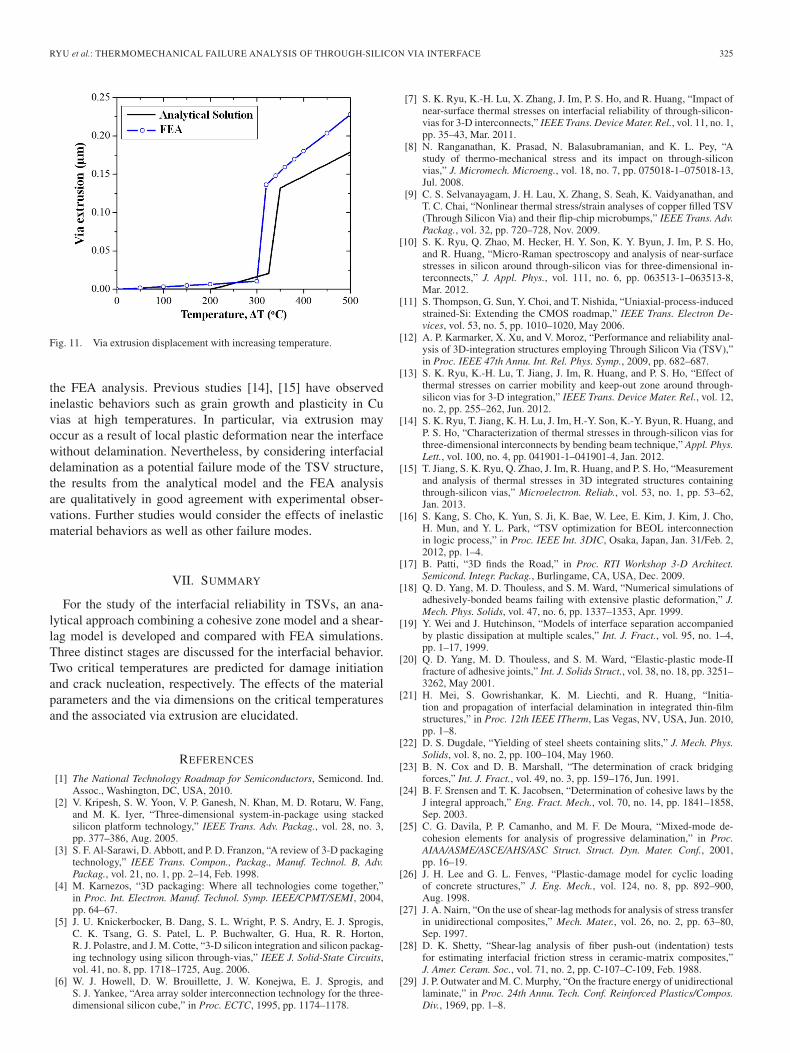
IV. CRITICAL TEMPERATURES FOR DEBONDING
Two critical temperatures are predicted by the cohesive zonemodel for interfacial failure of the TSV. For the convenienceof discussion, the physical and geometrical parameters arenormalized as follows:
Temperature change: ΔT = (αvia − αsub)ΔT (25)
Interfacial strength: τmax =τmax
Evia(26)
Interfacial Stiffness: K0 =K0Dvia
Evia(27)
Interfacial Toughness: Γ =Γ
EviaDvia(28)
Via height (aspect ratio): H =H
Dvia. (29)
The first critical temperature defines the temperature changewhen an initially intact TSV structure starts to accumulatedamage at the interface, forming a cohesive zone near the freesurface. By (13), the critical temperature after normalizationcan be expressed as a function of three dimensionless param-eters, H , τmax, and K0
ΔT c1 =2τmax√
K0
coth
(H
√K0
). (30)
Note that the first critical temperature (for damage initiation)is independent of the interfacial toughness, but depends on theinterfacial strength and the aspect ratio of the via. In the limitingcase for a high aspect ratio, H � 1, we have approximately
ΔT c1 ≈ 2τmax√K0
. (31)
The second critical temperature defines the temperaturewhen an interfacial crack starts to nucleate from the cohe-sive zone with a fully debonded region. By (20), the criticaltemperature is given implicitly. After normalization, it can beexpressed as a function of four dimensionless parameters, H ,Γ, τmax, and K0
ΔT c2 = f(Γ, τmax,K0, H). (32)
Fig. 4. (a) Critical temperatures for interfacial failure of the TSV structure;(b) Effect of via diameter on the second critical temperature.
Thus, the second critical temperature (for crack initiation) doesdepend on the interfacial toughness in addition to the other threeparameters. In the limiting case for a high aspect ratio, H � 1,we have approximately
ΔT c2 ≈√
8Γ. (33)
Similar results have been obtained previously for fiber-reinforced composites [29].
For an example, both critical temperatures are calculatedin this section by using the following properties for the TSVstructure with Dvia = 6 μm: Evia = 110 GPa, αvia − αsub =14.7 ppm/◦C, τmax = 150 MPa, Γ = 2.0 J/m2, and δi =10 nm. The normalized parameters as defined by (26)–(28) are
τ = 0.0013K0 = 0.81Γ = 3 × 10⁻⁶. (34)
The two critical temperatures are plotted in Fig. 4(a) as a func-tion of the via height, H . Both the critical temperatures increaseas H decreases for the case of relatively small via height (H <20 μm). For larger via height, the critical temperatures becomeindependent of H . By the approximate solutions in (31) and(33), the two critical temperatures are 196 ◦C and 333 ◦C forlarge via heights (H > 20 μm). It is noted that the normalizedparameters, K0 and Γ, depend on the via diameter (Dvia). As

322 IEEE TRANSACTIONS ON DEVICE AND MATERIALS RELIABILITY, VOL. 14, NO. 1, MARCH 2014
Fig. 5. Effect of interfacial toughness on the critical temperature (τmax =
0.0013 and K0 = 0.81).
the via diameter increases, K0 increases and Γ decreases. As aresult, by (31) and (33), both the critical temperatures decreaseif the via height (H) remains relatively large. As shown inFig. 4(b), the second critical temperature merges to a samecurve for both via diameters considered when the via height issmall (H < 10 μm), but decreases to a lower level for the largervia diameter when the via height is large. In particular, considera TSV structure subjected to a thermal load, ΔT = 300 ◦C.By Fig. 4(b), interfacial delamination would not occur in thesmaller via with Dvia = 6 μm, because ΔT < ΔTc2 for allvia heights. However, for the larger via with Dvia = 20 μm,interfacial delamination would occur if the via height is greaterthan a critical value (H > 20 μm).
The critical temperatures could be much lower for TSVs withlarger diameters, as shown in Fig. 4(b). For relatively large viaheight (H � 1), both the critical temperatures are inverselyproportional to the square root of Dvia, as predicted by (31)and (33). Furthermore, the effects of interfacial properties, suchas toughness and strength on the critical temperatures, wereinvestigated. Fig. 5 shows that the second critical temperaturebecomes lower as the interfacial toughness decreases. In con-trast, the first critical temperature is independent of the tough-ness as predicted by (30). In a previous study, we observed TSVextrusion due to local plastic deformation in the Cu vias [14].Toughness can be enhanced by material plasticity since plasticdeformation dissipates energy around the crack tip. Therefore,the second critical temperature would increase in the presenceof plastic deformation, and interfacial delamination would besuppressed when ΔT < ΔTc2.
The effect of interfacial strength on the critical temperatureis shown in Fig. 6. The first critical temperature increases withincreasing interfacial strength [Fig. 6(a)]. However, the secondcritical temperature shows an opposite trend. For a fixed inter-facial toughness, the second critical temperatures for differentinterfacial strengths converge to the same value for sufficientlylarge aspect ratios (H � 1), as predicted by (33) [Fig. 6(b)].For relatively small aspect ratios, the second critical tempera-ture depends on the interfacial strength. By the bilinear traction-separation relation (Fig. 2), for the same toughness, a higherinterfacial strength results in a smaller critical sliding separation(δf ) at the final failure. Consequently, the second critical tem-
Fig. 6. Effect of interfacial strength on the critical temperatures (Γ = 3 ×10⁻⁶ and K0 = 0.81): (a) First critical temperature; (b) Second criticaltemperature.
perature decreases with increasing interfacial strength. The sizeof the cohesive zone reaches a steady state when ΔT > ΔTc2,which decreases with increasing interfacial strength. If thecohesive zone size is small compared to the via depth (small-scale bridging), the result becomes independent of the strength.However, when the cohesive zone size is comparable to thedepth (large-scale bridging), the second critical temperaturedecreases with decreasing cohesive zone size. Therefore, ingeneral, both the strength and the toughness of the interfaceare needed to determine the interfacial reliability in the TSVstructures.
V. VIA EXTRUSION
The sliding displacement at the wafer surface may be ob-served as via extrusion. By the combination of the cohesivezone model and the shear-lag model, the sliding displacementat the surface (ξ = H/2) is determined as a function of thethermal load (ΔT ). In Stage I (ΔT < ΔTc1), by (11), theextrusion displacement is
δ̂ = λ (αvia − αsub)ΔT tanh
(H
2λ
). (35)
In this stage, since the interface remain intact, the extrusiondisplacement depends on the elastic properties of the via and

RYU et al.: THERMOMECHANICAL FAILURE ANALYSIS OF THROUGH-SILICON VIA INTERFACE 323
Fig. 7. Via extrusion displacement for various aspect ratios (a) after firstcritical temperature; (b) after second critical temperature by the shear-lag model; (c) via extrusion observed for various annealing temperatures(Source: [16]).
interface only, which is relatively small (δ̂ < δi). In Stage II(ΔTc1 < ΔT < ΔTc2), the extrusion displacement at the sur-face is given by
δ̂ = δf − (δf − δi) cos
(H/2 − l1
a
)
+δia
λcoth
(l1λ
)sin
(H/2 − l1
a
)(36)
where l1 is a function of ΔT by (18). Finally, in Stage III(ΔT > ΔTc2), the extrusion displacement is
δ̂ = δf +
(H
2− l2
)(αvia − αsub)ΔT (37)
Fig. 8. (a) Via extrusion for various via heights and diameters; (b) Experi-mental observation of via extrusion and interfacial delamination for differentvia diameters and depths (Source: [16]).
where l2 is a function of ΔT obtainable by solving (22) and(23) simultaneously.
Fig. 7 plots the extrusion displacement as a function of thethermal load. The extrusion displacement increases linearlyduring Stage I. At the first critical temperature [196 ◦C accord-ing to the result in Fig. 4(a)], the extrusion displacement kinksup to increase more rapidly in Stage II. At the second criticaltemperature (333 ◦C), the extrusion displacement increasesabruptly due to crack nucleation at the interface. Similar trendfor via extrusion was observed experimentally by Kang, et al.[16], as shown in Fig. 7(c). Furthermore, the extrusion displace-ment increases with the normalized via height, which suggeststhat wafer thinning (or reduction of the TSV height) can helpreduce via extrusion.
Via extrusion for various via diameters and heights (ordepths) is analytically calculated with ΔT = 300 ◦C [Fig. 8(a)].The numbers in the bubble plot indicate the magnitude ofvia extrusion (unit: μm). It was found that serious interfacialdelamination could occur for the vias with relatively largediameters and heights. Kang et al. reported experimental datafor via extrusion due to interfacial delamination [16]. Theexperimental trend in the study [Fig. 5(b)] is consistent withthe prediction by the analytical model in the present study eventhough the numbers in the axes were not provided.
VI. FINITE-ELEMENT ANALYSIS (FEA)
Finite-element models have been developed using ABAQUSto simulate the initiation and growth of interfacial delaminationin the TSV structure. All the constituent materials are assumed

324 IEEE TRANSACTIONS ON DEVICE AND MATERIALS RELIABILITY, VOL. 14, NO. 1, MARCH 2014
Fig. 9. Simulation of via extrusion during heating process: (a) ΔT = 100 ◦C;(b) ΔT = 280 ◦C; (c) ΔT = 350 ◦C.
to be linear elastic, while the interface between the via andSi is modeled by cohesive elements with the bilinear traction-separation relation. In the present study, an axisymmetric FEAmodel was used for computational efficiency. For the calcula-tion, the material properties listed in (34) were used. The viaand Si parts were meshed with 0.1 × 0.06 μm2 axisymmetricelement (CAX4R), while the interface was modeled with alayer of cohesive element (COHAX4). Fig. 9 shows the debond-ing process with increasing temperature. As expected fromthe analytical solution, the via extrusion dramatically increasesafter the second critical temperature [Fig. 9(c)].
Fig. 10(a) plots the interfacial damage variable, D alongthe depth (z/Dvia) from the FEA model with a fixed height(H/Dvia = 10) for different thermal loads. The damage vari-able remains zero everywhere until the first critical temperatureis reached. As predicted by the shear-lag model, the interfacialbehavior follows the linear elastic traction-separation relationin Stage I (ΔT < ΔTc1). For ΔT > ΔTc1, a damage zone
Fig. 10. Damage evolution with increasing temperature, ΔT : (a) Damagevariable vs. depth; (b) Damage variable at z = 0 vs. temperature (the red dashedlines indicate the two critical temperatures obtained from the shear-lag model).
emerges with 0 < D < 1 and grows along the interface. Themaximum damage variable at the surface/interface junction(z = 0) is less than 1 for ΔT < 326 ◦C. At the second criticaltemperature (ΔTc2 = 326 ◦C), a crack is nucleated with D = 1at the surface/interface junction. Subsequently, the crack growsalong the interface with a steady-state damage zone ahead ofthe crack tip. Fig. 10(b) plots the interfacial damage variableat the surface/interface junction (z = 0) as a function of thetemperature change, which shows clearly the two critical tem-peratures. For comparison, the critical temperatures predictedby the shear-lag model are indicated by the vertical dashedlines in Fig. 10(b). Apparently, the first critical temperature is∼200 ◦C according to the analytical solution, which is lowerthan the FEA calculation (∼280 ◦C). On the other hand, thesecond critical temperature predicted by the shear-lag model isin good agreement with the FEA result. The shear-lag modelpredicts it to be 333 ◦C at H/Dvia = 10, while the FEA modelpredicts 326 ◦C. Moreover, Fig. 11 compares the via extrusiondisplacement obtained from the FEA model with the predictionby the shear-lag model. The differences between the two mod-els can be attributed to the nonuniform stress distribution in thevia as shown in Fig. 9.
It is noted that the present study has assumed linear elasticityfor the via material and Si in both the analytical model and
RYU et al.: THERMOMECHANICAL FAILURE ANALYSIS OF THROUGH-SILICON VIA INTERFACE 325
Fig. 11. Via extrusion displacement with increasing temperature.
the FEA analysis. Previous studies [14], [15] have observedinelastic behaviors such as grain growth and plasticity in Cuvias at high temperatures. In particular, via extrusion mayoccur as a result of local plastic deformation near the interfacewithout delamination. Nevertheless, by considering interfacialdelamination as a potential failure mode of the TSV structure,the results from the analytical model and the FEA analysisare qualitatively in good agreement with experimental obser-vations. Further studies would consider the effects of inelasticmaterial behaviors as well as other failure modes.
VII. SUMMARY
For the study of the interfacial reliability in TSVs, an ana-lytical approach combining a cohesive zone model and a shear-lag model is developed and compared with FEA simulations.Three distinct stages are discussed for the interfacial behavior.Two critical temperatures are predicted for damage initiationand crack nucleation, respectively. The effects of the materialparameters and the via dimensions on the critical temperaturesand the associated via extrusion are elucidated.
REFERENCES
[1] The National Technology Roadmap for Semiconductors, Semicond. Ind.Assoc., Washington, DC, USA, 2010.
[2] V. Kripesh, S. W. Yoon, V. P. Ganesh, N. Khan, M. D. Rotaru, W. Fang,and M. K. Iyer, “Three-dimensional system-in-package using stackedsilicon platform technology,” IEEE Trans. Adv. Packag., vol. 28, no. 3,pp. 377–386, Aug. 2005.
[3] S. F. Al-Sarawi, D. Abbott, and P. D. Franzon, “A review of 3-D packagingtechnology,” IEEE Trans. Compon., Packag., Manuf. Technol. B, Adv.Packag., vol. 21, no. 1, pp. 2–14, Feb. 1998.
[4] M. Karnezos, “3D packaging: Where all technologies come together,”in Proc. Int. Electron. Manuf. Technol. Symp. IEEE/CPMT/SEMI, 2004,pp. 64–67.
[5] J. U. Knickerbocker, B. Dang, S. L. Wright, P. S. Andry, E. J. Sprogis,C. K. Tsang, G. S. Patel, L. P. Buchwalter, G. Hua, R. R. Horton,R. J. Polastre, and J. M. Cotte, “3-D silicon integration and silicon packag-ing technology using silicon through-vias,” IEEE J. Solid-State Circuits,vol. 41, no. 8, pp. 1718–1725, Aug. 2006.
[6] W. J. Howell, D. W. Brouillette, J. W. Konejwa, E. J. Sprogis, andS. J. Yankee, “Area array solder interconnection technology for the three-dimensional silicon cube,” in Proc. ECTC, 1995, pp. 1174–1178.
[7] S. K. Ryu, K.-H. Lu, X. Zhang, J. Im, P. S. Ho, and R. Huang, “Impact ofnear-surface thermal stresses on interfacial reliability of through-silicon-vias for 3-D interconnects,” IEEE Trans. Device Mater. Rel., vol. 11, no. 1,pp. 35–43, Mar. 2011.
[8] N. Ranganathan, K. Prasad, N. Balasubramanian, and K. L. Pey, “Astudy of thermo-mechanical stress and its impact on through-siliconvias,” J. Micromech. Microeng., vol. 18, no. 7, pp. 075018-1–075018-13,Jul. 2008.
[9] C. S. Selvanayagam, J. H. Lau, X. Zhang, S. Seah, K. Vaidyanathan, andT. C. Chai, “Nonlinear thermal stress/strain analyses of copper filled TSV(Through Silicon Via) and their flip-chip microbumps,” IEEE Trans. Adv.Packag., vol. 32, pp. 720–728, Nov. 2009.
[10] S. K. Ryu, Q. Zhao, M. Hecker, H. Y. Son, K. Y. Byun, J. Im, P. S. Ho,and R. Huang, “Micro-Raman spectroscopy and analysis of near-surfacestresses in silicon around through-silicon vias for three-dimensional in-terconnects,” J. Appl. Phys., vol. 111, no. 6, pp. 063513-1–063513-8,Mar. 2012.
[11] S. Thompson, G. Sun, Y. Choi, and T. Nishida, “Uniaxial-process-inducedstrained-Si: Extending the CMOS roadmap,” IEEE Trans. Electron De-vices, vol. 53, no. 5, pp. 1010–1020, May 2006.
[12] A. P. Karmarker, X. Xu, and V. Moroz, “Performance and reliability anal-ysis of 3D-integration structures employing Through Silicon Via (TSV),”in Proc. IEEE 47th Annu. Int. Rel. Phys. Symp., 2009, pp. 682–687.
[13] S. K. Ryu, K.-H. Lu, T. Jiang, J. Im, R. Huang, and P. S. Ho, “Effect ofthermal stresses on carrier mobility and keep-out zone around through-silicon vias for 3-D integration,” IEEE Trans. Device Mater. Rel., vol. 12,no. 2, pp. 255–262, Jun. 2012.
[14] S. K. Ryu, T. Jiang, K. H. Lu, J. Im, H.-Y. Son, K.-Y. Byun, R. Huang, andP. S. Ho, “Characterization of thermal stresses in through-silicon vias forthree-dimensional interconnects by bending beam technique,” Appl. Phys.Lett., vol. 100, no. 4, pp. 041901-1–041901-4, Jan. 2012.
[15] T. Jiang, S. K. Ryu, Q. Zhao, J. Im, R. Huang, and P. S. Ho, “Measurementand analysis of thermal stresses in 3D integrated structures containingthrough-silicon vias,” Microelectron. Reliab., vol. 53, no. 1, pp. 53–62,Jan. 2013.
[16] S. Kang, S. Cho, K. Yun, S. Ji, K. Bae, W. Lee, E. Kim, J. Kim, J. Cho,H. Mun, and Y. L. Park, “TSV optimization for BEOL interconnectionin logic process,” in Proc. IEEE Int. 3DIC, Osaka, Japan, Jan. 31/Feb. 2,2012, pp. 1–4.
[17] B. Patti, “3D finds the Road,” in Proc. RTI Workshop 3-D Architect.Semicond. Integr. Packag., Burlingame, CA, USA, Dec. 2009.
[18] Q. D. Yang, M. D. Thouless, and S. M. Ward, “Numerical simulations ofadhesively-bonded beams failing with extensive plastic deformation,” J.Mech. Phys. Solids, vol. 47, no. 6, pp. 1337–1353, Apr. 1999.
[19] Y. Wei and J. Hutchinson, “Models of interface separation accompaniedby plastic dissipation at multiple scales,” Int. J. Fract., vol. 95, no. 1–4,pp. 1–17, 1999.
[20] Q. D. Yang, M. D. Thouless, and S. M. Ward, “Elastic-plastic mode-IIfracture of adhesive joints,” Int. J. Solids Struct., vol. 38, no. 18, pp. 3251–3262, May 2001.
[21] H. Mei, S. Gowrishankar, K. M. Liechti, and R. Huang, “Initia-tion and propagation of interfacial delamination in integrated thin-filmstructures,” in Proc. 12th IEEE ITherm, Las Vegas, NV, USA, Jun. 2010,pp. 1–8.
[22] D. S. Dugdale, “Yielding of steel sheets containing slits,” J. Mech. Phys.Solids, vol. 8, no. 2, pp. 100–104, May 1960.
[23] B. N. Cox and D. B. Marshall, “The determination of crack bridgingforces,” Int. J. Fract., vol. 49, no. 3, pp. 159–176, Jun. 1991.
[24] B. F. Srensen and T. K. Jacobsen, “Determination of cohesive laws by theJ integral approach,” Eng. Fract. Mech., vol. 70, no. 14, pp. 1841–1858,Sep. 2003.
[25] C. G. Davila, P. P. Camanho, and M. F. De Moura, “Mixed-mode de-cohesion elements for analysis of progressive delamination,” in Proc.AIAA/ASME/ASCE/AHS/ASC Struct. Struct. Dyn. Mater. Conf., 2001,pp. 16–19.
[26] J. H. Lee and G. L. Fenves, “Plastic-damage model for cyclic loadingof concrete structures,” J. Eng. Mech., vol. 124, no. 8, pp. 892–900,Aug. 1998.
[27] J. A. Nairn, “On the use of shear-lag methods for analysis of stress transferin unidirectional composites,” Mech. Mater., vol. 26, no. 2, pp. 63–80,Sep. 1997.
[28] D. K. Shetty, “Shear-lag analysis of fiber push-out (indentation) testsfor estimating interfacial friction stress in ceramic-matrix composites,”J. Amer. Ceram. Soc., vol. 71, no. 2, pp. C-107–C-109, Feb. 1988.
[29] J. P. Outwater and M. C. Murphy, “On the fracture energy of unidirectionallaminate,” in Proc. 24th Annu. Tech. Conf. Reinforced Plastics/Compos.Div., 1969, pp. 1–8.
326 IEEE TRANSACTIONS ON DEVICE AND MATERIALS RELIABILITY, VOL. 14, NO. 1, MARCH 2014
Suk-Kyu Ryu received the B.S. and M.S. degrees inaerospace engineering from Korea Aerospace Uni-versity, Goyang, Korea, in 1998 and 2000, respec-tively, and the Ph.D. degree in aerospace engineeringand engineering mechanics from The University ofTexas at Austin, Austin, TX, USA, in 2011.
He had several years of working experience in thecomposite material industry, and he was a Researcherin a microsystem laboratory of Korea Institute of Sci-ence and Technology, Seoul, Korea. Currently, he isa Senior Engineer at Applied Materials, Sunnyvale,
CA, USA. His research interests are in the areas of thermomechanical process-related reliability issues in electronics materials and microelectronic packagingand coating materials for hardware under corrosive–erosive conditions.
Tengfei Jiang received the B.S. degree in materialsscience and engineering from Tsinghua University,Beijing, China, in 2006 and the M.S. degree inmaterials science and engineering from The OhioState University, Columbus, OH, USA, in 2009.Since 2010, she has been working toward the Ph.D.degree in materials science and engineering at TheUniversity of Texas at Austin, Austin, TX, USA.
Currently, her research is focused on the thermo-mechanical reliability of 3-D interconnects.
Jay Im received the B.S. degree in mechanical engineering from Seoul NationalUniversity, Seoul, Korea, and the M.S. degree in mechanical engineering andthe Doctoral degree in materials science and engineering from MassachusettsInstitute of Technology, Cambridge, MA, USA.
He is a Research Professor in the Laboratory for Interconnect and Packaging,The University of Texas at Austin, Austin, TX, USA. He has more than130 published papers and 9 U.S. patents. His current research areas are inelectronic package and reliability, 3-D through-silicon vias, electromigration ofsolder joints, and thin-film testing metrology. Up until 2004, he had been withThe Dow Chemical Company for 28 years, taking on various R&D positionsincluding Research Scientist in electronic materials, where he was headingmaterials science and adhesion efforts for BCB and SiLK dielectrics.
Paul S. Ho (M’91–SM’93–F’02) received the Ph.D.degree in physics from Rensselaer Polytechnic Insti-tute, Troy, NY, USA.
In 1966, he joined the Department of MaterialsScience and Engineering, Cornell University, Ithaca,NY, where he became an Associate Professor in1972. In 1972, he joined the IBM T. J. WatsonResearch Center and became the Senior Managerof the Interface Science Department in 1985. Since1991, he has been with the faculty of The Universityof Texas at Austin, Austin, TX, USA, where he was
appointed as the Cockrell Family Regents Chair in Materials Science andEngineering and is currently the Director of the Laboratory for Interconnectand Packaging. His current research is in the areas of materials and processingscience for interconnect and packaging applications.
Rui Huang received the B.S. degree in theoreti-cal and applied mechanics from the University ofScience and Technology of China, Hefei, China, in1994 and the Ph.D. degree in civil and environmentalengineering, with specialty in mechanics, materials,and structures, from Princeton University, Princeton,NJ, USA, in 2001.
In 2002, he joined the faculty at The Universityof Texas at Austin, Austin, TX, USA, where heis currently an Associate Professor of aerospaceengineering and engineering mechanics and holds
the position of Mrs. Pearlie Dashiell Henderson Centennial Fellowship inEngineering. His research interests include mechanics of integrated materialsand structures at micro- and nanoscales, reliability of advanced interconnectsand packaging for microelectronics, and mechanical instability of thin films andnanostructures.


![Thermomechanical Analysis [TMA] [NETZSCH]](https://static.fdocuments.in/doc/165x107/55cf940b550346f57b9f3bd8/thermomechanical-analysis-tma-netzsch.jpg)
