Thermography based online characterization of conductive...
11
Thermography based online characterization of conductive thin films in large-scale electronics fabrication KARI REMES, 1,* KIMMO LEPPÄNEN, 1,2 AND TAPIO FABRITIUS 1 1 Optoelectronics and Measurement Techniques, Faculty of Information Technology and Electrical Engineering, University of Oulu, Erkki Koiso-Kanttilankatu 3, 90570 Oulu, Finland 2 Currently with Mettler-Toledo GmbH, SBU AutoChem, Sonnenbergstrasse 74, 8603 Schwerzenbach, Switzerland *[email protected] Abstract: Flexible electronics is an emerging thin film based technology enabling completely new types of products and applications compared to conventional electronics. Since the quality of films defines the functionality of fabricated devices, the lack of suitable online manufacturing quality assessment tools has been identified to be a critical bottleneck while upscaling the volume and the yield of thin film electronics manufacturing. In order to solve that problem, a synchronized thermography (ST) based online measurement system was built. Applicability of proposed roll-to-roll compatible ST based system was demonstrated by characterizing a moving plastic film with conductive indium tin oxide on top. Obtained results show that ST can be utilized for online homogeneity characterization and sheet resistance estimation of large area thin films which are not possible with other existing methods. © 2018 Optical Society of America under the terms of the OSA Open Access Publishing Agreement OCIS codes: (110.6820) Thermal imaging; (310.3840) Materials and process characterization. References and links 1. S. J. Kim, A. L. K. Choi, B. Lee, Y. Kim, and B. H. Hong, “Materials for Flexible, Stretchable Electronics: Graphene and 2D Materials,” Annu. Rev. Mater. Res. 45(1), 63–84 (2015). 2. K. D. Harris, A. L. Elias, and H.-J. Chung, “Flexible electronics under strain: a review of mechanical characterization and durability enhancement strategies,” J. Mater. Sci. 51(6), 2771–2805 (2016). 3. K. Seshan, Handbook of Thin Film Deposition: Techniques, Processes, and Technologies (Elsevier, 2012). 4. B. Kumar, B. K. Kaushik, and Y. S. Negi, “Organic thin film transistors: Structures, models, materials, fabrication, and applications: A Review,” Polym. Rev. (Phila. Pa.) 54(1), 33–111 (2014). 5. H. E. Katz and J. Huang, “Thin-film organic electronic devices,” Annu. Rev. Mater. Res. 39(1), 71–92 (2009). 6. A. Alkhazaili, M. M. Hamasha, G. Choi, S. Lu, and C. R. Westgate, “Reliability of thin films: Experimental study on mechanical and thermal behavior of indium tin oxide and poly(3,4-ethylenedioxythiophene),” Microelectron. Reliab. 55(3–4), 538–546 (2015). 7. L. Ke, R. S. Kumar, S. J. Chua, and A. P. Burden, “Degradation study in flexible substrate organic light-emitting diodes,” Appl. Phys., A Mater. Sci. Process. 81(5), 969–974 (2005). 8. M. Fried, “On-line monitoring of solar cell module production by ellipsometry technique,” Thin Solid Films 571, 345–355 (2014). 9. I. Poliski, “Thin Film is What You Make It: New Angles on Deposition,” R&D Magazine 43(8), 26–33 (2001). 10. J. C. Li, Y. Wang, and D. C. Ba, “Characterization of semiconductor surface conductivity by using microscopic four-point technique,” Phys. Procedia 32, 347–355 (2012). 11. J. R. Lee, D. Y. Lee, D. G. Kim, G. H. Lee, Y. D. Kim, and P. K. Song, “Characteristics of ITO Films Deposited on a PET Substrate Under Various Deposition Conditions,” Met. Mater. Int. 14(6), 745–751 (2008). 12. J.-W. Park, G. Kim, S.-H. Lee, E.-H. Kim, and G.-H. Lee, “The effect of film microstructures on cracking of transparent conductive oxide (TCO) coatings on polymer substrates,” Surf. Coat. Tech. 205(3), 915–921 (2010). 13. W. F. Stickle, “Applying Surface Analysis in Electronics Materials Processing,” J. Surf. Anal. 14(4), 406–411 (2008). 14. K. Shimanovich, Y. Bouhadana, D. A. Keller, S. Rühle, A. Y. Anderson, and A. Zaban, “Four-point probe electrical resistivity scanning system for large area conductivity and activation energy mapping,” Rev. Sci. Instrum. 85(5), 055103 (2014). 15. O. Breitenstein, W. Warta, and M. Langenkamp, Lock-in Thermography: Basics and Use for Evaluating Electronic Devices and Materials (Springer, 2010). 16. D. Kendig, G. B. Alers, and A. Shakouri, “Thermoreflectance imaging of Defects in Thin-film Solar Cells,” in Proceedings of 2010 IEEE International Reliability Physics Symposium (IEEE, 2010), pp. 499–502. Vol. 26, No. 2 | 22 Jan 2018 | OPTICS EXPRESS 1219 #314127 Journal © 2018 https://doi.org/10.1364/OE.26.001219 Received 4 Dec 2017; revised 30 Dec 2017; accepted 2 Jan 2018; published 11 Jan 2018
Transcript of Thermography based online characterization of conductive...

Thermography based online characterization of conductive thin films in large-scale electronics fabrication
KARI REMES,1,* KIMMO LEPPÄNEN,1,2 AND TAPIO FABRITIUS1 1Optoelectronics and Measurement Techniques, Faculty of Information Technology and Electrical Engineering, University of Oulu, Erkki Koiso-Kanttilankatu 3, 90570 Oulu, Finland 2Currently with Mettler-Toledo GmbH, SBU AutoChem, Sonnenbergstrasse 74, 8603 Schwerzenbach, Switzerland *[email protected]
Abstract: Flexible electronics is an emerging thin film based technology enabling completely new types of products and applications compared to conventional electronics. Since the quality of films defines the functionality of fabricated devices, the lack of suitable online manufacturing quality assessment tools has been identified to be a critical bottleneck while upscaling the volume and the yield of thin film electronics manufacturing. In order to solve that problem, a synchronized thermography (ST) based online measurement system was built. Applicability of proposed roll-to-roll compatible ST based system was demonstrated by characterizing a moving plastic film with conductive indium tin oxide on top. Obtained results show that ST can be utilized for online homogeneity characterization and sheet resistance estimation of large area thin films which are not possible with other existing methods. © 2018 Optical Society of America under the terms of the OSA Open Access Publishing Agreement
OCIS codes: (110.6820) Thermal imaging; (310.3840) Materials and process characterization.
References and links
1. S. J. Kim, A. L. K. Choi, B. Lee, Y. Kim, and B. H. Hong, “Materials for Flexible, Stretchable Electronics: Graphene and 2D Materials,” Annu. Rev. Mater. Res. 45(1), 63–84 (2015).
2. K. D. Harris, A. L. Elias, and H.-J. Chung, “Flexible electronics under strain: a review of mechanical characterization and durability enhancement strategies,” J. Mater. Sci. 51(6), 2771–2805 (2016).
3. K. Seshan, Handbook of Thin Film Deposition: Techniques, Processes, and Technologies (Elsevier, 2012). 4. B. Kumar, B. K. Kaushik, and Y. S. Negi, “Organic thin film transistors: Structures, models, materials,
fabrication, and applications: A Review,” Polym. Rev. (Phila. Pa.) 54(1), 33–111 (2014). 5. H. E. Katz and J. Huang, “Thin-film organic electronic devices,” Annu. Rev. Mater. Res. 39(1), 71–92 (2009). 6. A. Alkhazaili, M. M. Hamasha, G. Choi, S. Lu, and C. R. Westgate, “Reliability of thin films: Experimental
study on mechanical and thermal behavior of indium tin oxide and poly(3,4-ethylenedioxythiophene),” Microelectron. Reliab. 55(3–4), 538–546 (2015).
7. L. Ke, R. S. Kumar, S. J. Chua, and A. P. Burden, “Degradation study in flexible substrate organic light-emitting diodes,” Appl. Phys., A Mater. Sci. Process. 81(5), 969–974 (2005).
8. M. Fried, “On-line monitoring of solar cell module production by ellipsometry technique,” Thin Solid Films 571, 345–355 (2014).
9. I. Poliski, “Thin Film is What You Make It: New Angles on Deposition,” R&D Magazine 43(8), 26–33 (2001). 10. J. C. Li, Y. Wang, and D. C. Ba, “Characterization of semiconductor surface conductivity by using microscopic
four-point technique,” Phys. Procedia 32, 347–355 (2012). 11. J. R. Lee, D. Y. Lee, D. G. Kim, G. H. Lee, Y. D. Kim, and P. K. Song, “Characteristics of ITO Films Deposited
on a PET Substrate Under Various Deposition Conditions,” Met. Mater. Int. 14(6), 745–751 (2008). 12. J.-W. Park, G. Kim, S.-H. Lee, E.-H. Kim, and G.-H. Lee, “The effect of film microstructures on cracking of
transparent conductive oxide (TCO) coatings on polymer substrates,” Surf. Coat. Tech. 205(3), 915–921 (2010). 13. W. F. Stickle, “Applying Surface Analysis in Electronics Materials Processing,” J. Surf. Anal. 14(4), 406–411
(2008). 14. K. Shimanovich, Y. Bouhadana, D. A. Keller, S. Rühle, A. Y. Anderson, and A. Zaban, “Four-point probe
electrical resistivity scanning system for large area conductivity and activation energy mapping,” Rev. Sci. Instrum. 85(5), 055103 (2014).
15. O. Breitenstein, W. Warta, and M. Langenkamp, Lock-in Thermography: Basics and Use for Evaluating Electronic Devices and Materials (Springer, 2010).
16. D. Kendig, G. B. Alers, and A. Shakouri, “Thermoreflectance imaging of Defects in Thin-film Solar Cells,” in Proceedings of 2010 IEEE International Reliability Physics Symposium (IEEE, 2010), pp. 499–502.
Vol. 26, No. 2 | 22 Jan 2018 | OPTICS EXPRESS 1219
#314127 Journal © 2018
https://doi.org/10.1364/OE.26.001219 Received 4 Dec 2017; revised 30 Dec 2017; accepted 2 Jan 2018; published 11 Jan 2018

17. K. Leppänen, J. Saarela, R. Myllylä, and T. Fabritius, “Electrical heating synchronized with IR imaging to determine thin film defects,” Opt. Express 21(26), 32358–32370 (2013).
18. K. Leppänen, J. Saarela, and T. Fabritius, “IR-imaging based system for detecting the defects of conductive materials,” Proc. SPIE 9205, 92050M (2014).
19. K. Leppänen, J. Saarela, and T. Fabritius, “Synchronized thermography for multilayer thin film characterization,” Proc. SPIE 9177, 917705 (2014).
20. C. Schuss, K. Leppänen, K. Remes, J. Saarela, T. Fabritius, B. Eichberger, and T. Rahkonen, “Detecting Defects in Photovoltaic Cells and Panels and Evaluating the Impact on Output Performances,” IEEE Trans. Instrum. Meas. 65(5), 1108–1119 (2016).
21. K. Leppänen, Sample Preparation Method and Synchronized Thermography to Characterize Uniformity of Conductive Thin Films (University of Oulu, 2015).
1. Introduction
Our future will be filled with flexible, bendable and stretchable electronics capable of monitoring our living environment, status of personal wellbeing and entertaining us, if the visionaries and analytics are to be believed. Technology developers are constantly bringing out materials and components making a diverse set of devices with unique features possible, such as flexible consumer electronics, structural electronics for automotive industry, wearable sensors for healthcare etc [1, 2]. Thin film technologies have got an import role as an enabler of these applications, and conductive thin films are already being exploited in several type of products such as displays, solar cells and touch panels [3–5]. Flexibility and transparency of materials are often required in these applications. Another important property is uniformity, so problems with thin film uniformity will become an issue. For example small, invisible defects (cracks or pinholes) on a film have a significant effect on electrical resistance of material influencing on the eventual device performance as well [6, 7]. Since thin films have several favorable properties to be utilized in electronics, their significance is most likely to increase in the future.
Thin film quality assurance, which includes e.g. dimension measurements, roughness estimation, optical and electrical uniformity characterization, is essential for successful fabrication. Those measurements are performed to optimize the manufacturing processes and to ensure quality of the products since they enable detection, control and elimination of potential quality issues [3]. In large-area, high-volume production, where offline sampling and inspection is not practical due to the demanding price-performance requirements, online techniques are self-evident. For the best utilization, uniformity should be measured inline as part of the manufacturing process quality control. In high throughput production like roll-to-roll (R2R) environment, tens or more measurements are needed to obtain an acceptable level of characterization [8,9].
Numerous characterization techniques having potential for uniformity inspection of thin films have been proposed: electrical measurements such as four point probe method for conductivity as well as optical microscopy, profilometry, atomic force microscopy, X-ray photoelectron spectroscopy, spectroscopic ellipsometry, and electron microscopy for topological and dimensional characterization [3, 8, 10–13]. Unfortunately, these methods are typically intended for areas on nanometer to millimeter scale only thus encountering challenges with large area samples. In order to achieve reasonable spatial resolution and coverage, automated inspection processes are needed as has been done for the four point probe method [14], increasing the complexity of the measurement system. Despite of these automatization efforts, characterization of large-area samples is still time-consuming and typically non-compatible for online measurements. In addition to that, most of those techniques are limited to reveal issues on the surface of films only.
Combining optical infrared (IR) imaging with heating has shown to be an effective method for thin film uniformity characterization. In so called lock-in thermography technique, the characterized samples are heated with a modulated electrical signal or laser pulse less than few seconds, and IR imaging is synchronized with heating to analyze temperature variation of the samples [15]. Lock-in thermography based thermoreflectance imaging technique has been used successfully e.g. for detecting defects in thin film solar cells [16]. Lock-in thermography can achieve very good temperature and spatial resolution but it is
Vol. 26, No. 2 | 22 Jan 2018 | OPTICS EXPRESS 1220

unnecessarily complex making it impractical to be utilized in real online production environments.
Recently introduced synchronized thermography (ST) is another IR imaging based characterization method [17,18]. Here electrical heating of the sample with direct current (DC) power for several seconds is synchronized with IR imaging to produce thermograms. Non-uniformities on electrical conductivity in the film will influence on the current density characteristics varying the captured temperature profiles around it. Only a very simple and straightforward data processing is needed to localize and categorize defects on samples. ST has already shown to be a versatile technique to inspect the uniformity of large area thin films and evaluate the features of more complex structures such as solar cells [17–20]. Synchronized thermography can provide information about the degree of breakage on samples, and even estimate thin film conductivity and power efficiency of solar cell panels. Leppänen discussed in his PhD thesis [21] how to install ST into roll-to-roll environments. However, previous studies applying the ST method were made with stationary samples. In this study, the performance and applicability of the ST technique in a realistic R2R production environment with continuously moving samples, were successively demonstrated and evaluated for the first time.
2. Materials and methods
2.1 Samples
In order to demonstrate the performance of developed online measurement system, indium tin oxide (ITO) film was used as sample material. ITO was chosen because of its well-known properties, wide range of applications and good availability.
The commercially made sample material consists of ITO on polyethylene terephthalate (PET) film purchased from Solutia - CPFilms Inc., article OC50. Nominal thickness of the PET film is 125 μm. Nominal sheet resistance of the optically clear ITO coating is 40-60 Ω/ (ohms per square) with nominal thickness of 125 nm. The ITO on PET material was delivered as a roll with a width of 305 mm.
From the PET-ITO roll, a sheet with length of 1.5 m was cut. This sheet was then split in half in lengthwise direction thus yielding two 15 cm wide samples. The ends of a sample sheet were placed so that they overlapped each other 6.5 cm, and were then fixed with an adhesive tape, thus making an endless belt with a length of 143.5 cm. This procedure was done so that ITO stayed on the outside surface of the continuous sample web.
The first sample S1 was handled carefully during the measurement procedure in order to avoid any unnecessary mechanical stress, whereas the other sample S2 was intentionally treated mechanically by bending and twisting. The presumption is that the former sample should be practically undamaged while the latter one must have different kinds of defects in the brittle ITO layer.
2.2 Online thermography system
The objective of the study was to build a characterization system which is able to detect possible defects and uniformity of a moving conductive thin film. The designed and implemented measurement system follows R2R principles. The setup consists of an IR camera and a roller system as well as power sources and a computer as shown in Fig. 1.
An essential part of the system is the electrical heating unit for the conductive thin film. This heating unit consists of two metal coated disks located on the same axle, 5 cm apart from each other, and two rollers which press the sample film against the disks. Electrical current is applied from the DC power source run in constant current mode to the metal disks by coal brushes, and the disks then conduct electricity to the sample. Heating power is primarily set by adjusting the applied voltage. For measurements, the power was set to about 4 W which was found to be a practical value in preliminary ST studies. The aim was to heat a sample so that its temperature rises 2 to 8°C above ambient temperature. At the present setup, total
Vol. 26, No. 2 | 22 Jan 2018 | OPTICS EXPRESS 1221

length of the heated area is about 12 cm. If needed, this length - and also the heating time – can be modified by changing the distance between the two rollers.
In addition, there is a third roller which moves the sample. This roll has an electric motor connected to its’ axle by a belt drive. Drive speed of the sample ribbon is adjusted by changing the parameters of another DC power source. Speed of the belt was set to 1.3-1.4 cm/s for the sample test runs which match speed of a realistic R2R environment. As described, the driving speed of the sample belt is adjustable and can thus be set higher if needed.
Fig. 1. Schema of the developed roll-to-roll compatible online thermography setup.
An IR camera is located so that it capture images from the part of heated area of the sample between the metal plated disks as shown in Fig. 1. In this setup, the camera was a commercially available optris PI 640 thermal camera which captures video using a resolution of 640 x 480 pixels and frequency of 32 Hz with 256 temperature levels. The camera is controlled by a proprietary software which was set so that raw data was recorded without any image processing to achieve the fastest possible imaging.
2.3 IR imaging and image pretreatment procedure
The imaging procedure was initiated by switching on the movement of the sample, and recording a short (about 5 second) video of the moving sample without heating before each test run. This reference data was then stored to a temporary 3D image matrix R with a frame size of 640 x 480 pixels, where the number of image frames equals the frequency rate of the camera times the length of the video in seconds. A region of interest (ROI) of 1 x 250 pixels was selected for each frame of the matrix R at the same position between the heating disks. Mean of these ROIs was stored to a vector Trt(y) where y is the number of pixels perpendicular to the web direction, to represent the sample specific reference temperature for further calculations.
Actual infrared imaging was then started by switching on electrical heating of the moving sample web. A video sequence of one round of the sample web was then taken by the IR camera. The video was stored to a temporary 3D image matrix S with a frame size of 640 x 480 pixels, where the number of image frames again equals the frequency rate of the camera times the length of the video in seconds. As for the temperature reference above, a region of interest (ROI) of 1 x 250 pixels was then selected from each frame of the matrix S at the same position as for the temperature reference to an image Textracted(x,y) where x is the number of image frames and y is the same as for the reference. The ambient temperature stored in the
Vol. 26, No. 2 | 22 Jan 2018 | OPTICS EXPRESS 1222

vector Trt(y) was then subtracted from the ROI image temperature values to yield a temperature map Tp(x,y) of the sample belt as shown in Eq. (1).
( ) ( ) ( )
p extracted rtT x, y T x, y – T y , where x 1, 2, number of frames ,
and y 1, 2, 250
= ∈ …
∈ …
(1)
The resulting image is a pseudo-colored IR image which shows temperature variance above the ambient temperature with a distinct contrast. Figure 2 presents this procedure and also shows an example of a sample image.
Fig. 2. IR imaging and image pretreatment procedure as well as a sample IR image: a) Original sample and reference video frames, region of interest (ROI), subtraction of the ambient temperature, collecting of data, and pseudo-coloring; b) Location of the IR image on the moving sample belt, and an example of a sample IR image map.
The position of the ROI corresponds to a sample heating time of 8 seconds in lengthwise direction of a belt. A line-shaped ROI was used here to avoid problems with emissivity change caused by the angle of view. The location of the ROI was selected so that the areas proximity to the heating disks were left out to exclude temperature diffusion beside the disks and possible reflections. The height of the ROI and thus the height of a sample IR image corresponds to 46 mm on a sample. The length of an IR image corresponds to the length of a sample belt (143.5 cm) so the actual size of captured images covers an area of 660 cm2.
2.4 IR image analyzing procedure for uniformity characterization
To estimate the uniformity of a conductive thin film and analyze the difference between the carefully handled and the mechanically treated samples, a numerical value ΔT(x) was defined from captured IR images. ΔT(x) is the difference between the maximum and the minimum temperatures of a vertical line (a column) in an image map of a sample as stated in Eq. (2).
( ) ( ) ( )
p pT x max T x, y – min T x, y | y 1, 2, 250 ,
where x 1, 2, number of frames
Δ = ∈ …
∈ …
(2)
Vol. 26, No. 2 | 22 Jan 2018 | OPTICS EXPRESS 1223
ΔT(x) is useful to localize defected areas on sample web as shown later in this article.
2.5 Reference measurement of resistance
Four-wire technique was selected to measure reference values for the resistance of samples. This technique is commonly used for resistances smaller than 1000 ohms. The used equipment included an Agilent 34401A multimeter which support the 4-wire technique as well as two probes which were fixed to have a distance of 50 mm between each other. The resistance was measured on 24 locations (with constant distance) along a sample web and also separately for one selected location of a sample. On each location, three measurements were conducted and mean of the three measurement values was calculated to estimate of the resistance of film at that location.
3. Results
3.1 IR images of the samples
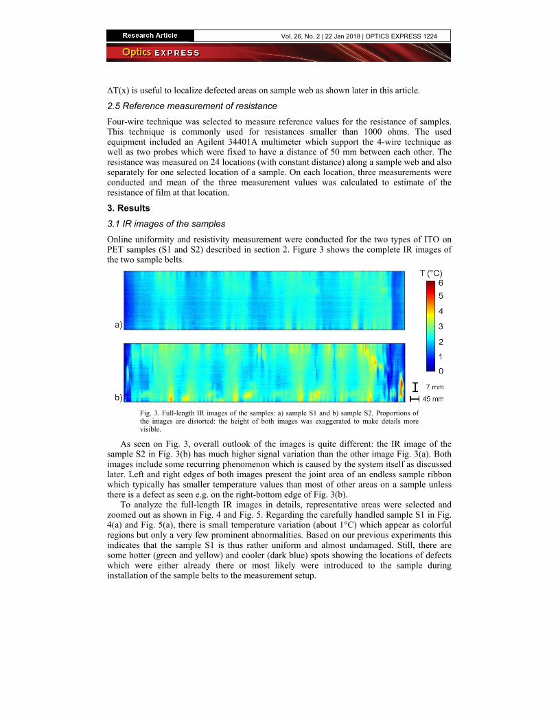
Online uniformity and resistivity measurement were conducted for the two types of ITO on PET samples (S1 and S2) described in section 2. Figure 3 shows the complete IR images of the two sample belts.
Fig. 3. Full-length IR images of the samples: a) sample S1 and b) sample S2. Proportions of the images are distorted: the height of both images was exaggerated to make details more visible.
As seen on Fig. 3, overall outlook of the images is quite different: the IR image of the sample S2 in Fig. 3(b) has much higher signal variation than the other image Fig. 3(a). Both images include some recurring phenomenon which is caused by the system itself as discussed later. Left and right edges of both images present the joint area of an endless sample ribbon which typically has smaller temperature values than most of other areas on a sample unless there is a defect as seen e.g. on the right-bottom edge of Fig. 3(b).
To analyze the full-length IR images in details, representative areas were selected and zoomed out as shown in Fig. 4 and Fig. 5. Regarding the carefully handled sample S1 in Fig. 4(a) and Fig. 5(a), there is small temperature variation (about 1°C) which appear as colorful regions but only a very few prominent abnormalities. Based on our previous experiments this indicates that the sample S1 is thus rather uniform and almost undamaged. Still, there are some hotter (green and yellow) and cooler (dark blue) spots showing the locations of defects which were either already there or most likely were introduced to the sample during installation of the sample belts to the measurement setup.
Vol. 26, No. 2 | 22 Jan 2018 | OPTICS EXPRESS 1224

Fig. 4. Detailed IR images along the samples: a) sample S1, and b) sample S2. Proportions of these detailed images are correct. Each detailed image is equivalent to an area of 46 mm x 46 mm on a sample.
Fig. 5. Selected detailed IR images of the samples: a) a decent-looking area on the sample S1, and b) an area with IR visible defects on the sample S2. Proportions of these detailed images are correct. Each detailed image is equivalent to an area of 46 mm x 46 mm on a sample.
Characteristics of the thermal images is quite different with the mechanically stressed sample S2: there are lots of hotter and cooler areas visible shown as colorful (red, yellow) spots, and temperature variations of the images are much larger (several degrees at maximum) than for the former sample. Temperature behavior proximity to a defect is similar as in previously done static measurements: a defected area itself is cool, and there is a hotter areas above and below a defect [17]. As these temperature variations indicate the presence of defects, the sample S2 clearly has much more defects than the sample S1. The images of the sample S2 include many areas with defects: small spot-like defects, larger-sized defects, and
Vol. 26, No. 2 | 22 Jan 2018 | OPTICS EXPRESS 1225

even long, scratch-like damaged areas which seem to consist of subsequent small spot defects.
3.2 ΔT(x) values of the samples
As described in section 2, a value ΔT(x) is now used to quantify the homogeneity of the thin films. Table 1 presents several statistical values of ΔT(x) for the samples S1 and S2, and Fig. 6 shows out calculated ΔT(x) values as line charts for the sample image data presented earlier in Fig. 5. The area where two ends of each sample belt are attached and thus overlapped, was intentionally left out of the following analysis.
Differences between the ΔT(x) statistics of the two samples are obvious. Mean and median values for the sample S2 are clearly (50% or more) higher than for the sample S1. ΔT(x) variation of the sample S2 is at least 35% larger than the variation of the sample S1. If ΔT(x) limit is set to 1.5 (degrees), only one percent of the full-length data values for the sample S1 are above this limit, whereas for the sample S2 almost 30% of the values stay above the same limit. Similarly, if a limit is set to 1.25, less than five percent of the values for the sample S1 and almost half of the values for the sample S2 raise above the limit. These differences are even more evident for the selected areas of the samples: the mean and median values for a defected area on S2 are at least 120% higher, and the variation almost 75% larger than for a decent looking area on S1. Thus, ΔT(x) values of the sample S2 are considerably larger and contain more variation than the data values of the sample S1. Using of a ΔT(x) limit – in this case for example value 1.25 – seems a workable way to detect problematic areas of samples in lengthwise direction of an ITO on PET web.
Table 1. Statistical values of the ΔT(x) data.
S1 (full-
length data) S2 (full-
length data) S1 (selected
data in Fig. 6a) S2 (selected data
in Fig. 6b) mean 0.848 1.343 0.782 1.763 median 0.806 1.221 0.769 1.719 standard deviation 0.200 0.428 0.134 0.524 coefficient of variation [%] 23.6 31.9 17.1 29.7 over limit of 1.5°C 1.0% 28.5% 0.0% 62.7% over limit of 1.25°C 4.9% 46.3% 0.0% 80.9% over limit of 1.0°C 17.9% 79.9% 3.7% 94.5%
The charts of Fig. 6 present many typical features of the results in details.
Fig. 6. ΔT(x) values of selected areas of the samples shown in Fig. 5; a) a decent-looking area on the sample S1; b) an area with IR visible defects on the sample S2.
The ΔT(x) value of a uniform-looking IR image of Fig. 5(a) stays quite constant although there is some noise on the data as seen in Fig. 6(a). As described above, the IR camera was recording raw video without any averaging and thus some noise is present in the images. Figure 6(b) then shows some typical ΔT(x) characteristics of defects. Here defected areas are seen as peaks but the shape of these peaks can be varying. Depending on the size and the location of defects, there are sharp peaks such as the peak around location 125.5 cm and
Vol. 26, No. 2 | 22 Jan 2018 | OPTICS EXPRESS 1226

126.2 cm with large ΔT(x) gradients or a wider peak with high ΔT(x) value around the location 128 cm.
Figure 7 presents the mean of ΔT(x) values for four consecutive runs of the samples S1 and S2. Values of both the full-length samples as well as the detailed areas are shown there. These runs were carried out to get an understanding of the consistency of the ΔT(x) values.
Fig. 7. Mean of ΔT(x) values for the samples S1 and S2; a) full-length sample data; b) selected detailed areas (some images shown in Fig. 5 and data in Fig. 6).
As depicted in Fig. 7(a), the mean ΔT(x) values stay on the same level during all the runs, although there is some small variation on ΔT(x) values of the full-length data. The same applies also to the uniform-looking area of the sample S1 as shown in Fig. 7(b). Besides ensuring that the presented ST technique is useful, this behavior also proposes that the system does not harm the samples. The mean of ΔT(x) for the area of the sample S2 with many IR visible defects shown in Fig. 7(b) varies slightly more probably because of the used heating arrangement.
In section 3.1 it was observed that the full-length images of the samples had some periodic noise characteristics, and it can be also found in the ΔT(x) data. Analysis of the measurement system revealed that this phenomenon corresponds the dimension of the copper disks of the heating system. The issue it is discussed more in the last section of this paper.
3.3 Correlation between ΔT(x) and electrical resistance
Both Table 1 and Fig. 7 prove that there is clearly distinguishable differences in the ΔT(x) values of differently handled samples (S1 and S2). By setting a threshold value for ΔT(x), the locations of defected areas can be identified and their influence on electrical performance can be quantified. The temperature difference may also reveal some other properties thin film such as heat transfer coefficient but these are not in the scope of this paper. Figure 8 presents the mean of ΔT(x) and the reference resistance values for the samples.
Figure 8 shows strong positive correlation between the mean ΔT(x) and measured resistance. Deviation of the resistance value is low (below 4 ohms) for all cases except for the full-length sample S2. For the selected detailed areas of the sample S1, the ΔT(x) is about 0.8 and the resistance is approximately 42 ohms. Similarly, the ΔT(x) of S2 (detail) is almost 1.8 and the resistance value is about 89 ohms. This suggests that the mean ΔT(x) values can be used to evaluate electrical properties of thin films, especially the degradation of resistance.
Vol. 26, No. 2 | 22 Jan 2018 | OPTICS EXPRESS 1227

Fig. 8. Measured resistance and calculated mean of ΔT(x) values of the full-length data [marked with (full)] and the selected detailed areas found in Fig. 5 [marked with (detail)] for the samples S1 and S2. Deviation of the resistance is included as bars.
4. Discussion and conclusion
In this paper, two differently handled ITO on PET films were selected as sample material to represent conductive thin films. These two samples were placed to the measurement setup in turn and thermal imaging procedure was conducted. During data capturing, all unnecessary data processing features such as averaging were set off to ensure the fastest possible analysis and feedback loop. Despite the fact that raw data is corrupted with some noise, the implemented system was capable to provide descent IR images of a whole sample area and the reconstructed still IR images from a video of a moving thin film are good enough to make reliable uniformity and defect localization analysis possible.
ST based analysis revealed defects on both samples: the intentionally damaged sample showed more defects with different types while the defects of the carefully handled sample appeared to be smaller and fewer. The latter defects were most probably caused during the installation of the sample to the R2R test setup. These observations were quantified by calculating the ΔT(x) value which indicates reasonably well many types of defects, and is thus capable of giving a trustable estimate of sample homogeneity. It is worth mentioning that ΔT(x) behavior stays similar over several measurement cycles of a sample indicating that the heating disks or the other parts of the system do not damage the sample. In addition, the mean values of ΔT(x) were found to have strong positive correlation with the measured reference resistance values showing that ST method can be used for online electrical conductivity analysis of thin films in R2R manufacturing environment. For a quantitative conductivity evaluation by this technique, also the mean temperature increase of a thin film should be taken into account along with the ΔT(x) value.
Calculation of ΔT(x) in this study was already very straightforward, and leaving the temperature reference (which is not compulsory for ΔT(x) calculations) out would simplify the procedure further - and thus ensuring that ΔT(x) is well suitably for online applications and process control. Mathematically simple ΔT(x) value can be calculated continuously and in real-time with a decent computer. By setting a suitable threshold, ΔT(x) is reasonable to indicate the location of suspicious areas of a sample instantly when a defect passes the measurement point.
In this study, an IR camera with a fixed focal length optics was used to image the samples. It’s well known that the focal length of the optics defines the angular field of view. Basically this means that it defines how wide area of the sample the camera sees, and what is the imaging resolution. The speed of a sample web and the imaging speed of the camera affect to the resolution in length-wise direction. As stated earlier, the resolution of the images
Vol. 26, No. 2 | 22 Jan 2018 | OPTICS EXPRESS 1228

produced by the existing measurement setup is good enough to reveal defects on samples. Imaging resolution can be improved by modifying the optics of the setup if needed. Depending on the case, imaging of a wide sample area with very good resolution might require a setup with multiple IR cameras.
The periodic noise in IR images appears to be mainly caused by the disks needed for electrical heating and the power source of the heating system. Those problems are difficult to avoid in the existing setup but their influence can be compensated by digital filtering. However, it was not seen necessary for the cases reported in this paper. Despite of the shortcomings, the current measurement concept and setup works already. Still, further research and development has to be done to release the full potential of the ST technique for large area applications.
In contrast to the previously performed static ST measurements, uniformity and conductivity measurements are more challenging to conduct since the sample web is in continuous movement. ST was shown to work well for brittle ITO on PET so it can be expected to work also for other similar conductive thin films making it a versatile method for large area thin film characterization. To explore the applicability of the ST technology, further studies are needed - also with more complex structures such as organic light emitting diodes (OLED). Thanks to its capabilities, the proposed synchronized thermography based method has a remarkable advantage over traditional measurement techniques dedicated for electrical measurements of large area thin films.
Funding
Partly funded by the European Metrology Programme for Innovation and Research (EMPIR) initiative Grant Agreement (14IND09).
Vol. 26, No. 2 | 22 Jan 2018 | OPTICS EXPRESS 1229