Thermoelectric properties of solution synthesized n … · Thermoelectric properties of solution...
18
Thermoelectric properties of solution synthesized n-type Bi 2 Te 3 nanocomposites modulated by Se: An experimental and theoretical study Haiyu Fang 1,† , Je-Hyeong Bahk 2,‡ , Tianli Feng 3 , Zhe Cheng 4 , Amr M. S. Mohammed 2 , Xinwei Wang 4 , Xiulin Ruan 3 , Ali Shakouri 2 , and Yue Wu 5 ( ) Nano Res., Just Accepted Manuscript • DOI: 10.1007/s12274-015-0892-x http://www.thenanoresearch.com on September 6 2015 © Tsinghua University Press 2015 Just Accepted This is a “Just Accepted” manuscript, which has been examined by the peer-review process and has been accepted for publication. A “Just Accepted” manuscript is published online shortly after its acceptance, which is prior to technical editing and formatting and author proofing. Tsinghua University Press (TUP) provides “Just Accepted” as an optional and free service which allows authors to make their results available to the research community as soon as possible after acceptance. After a manuscript has been technically edited and formatted, it will be removed from the “Just Accepted” Web site and published as an ASAP article. Please note that technical editing may introduce minor changes to the manuscript text and/or graphics which may affect the content, and all legal disclaimers that apply to the journal pertain. In no event shall TUP be held responsible for errors or consequences arising from the use of any information contained in these “Just Accepted” manuscripts. To cite this manuscript please use its Digital Object Identifier (DOI®), which is identical for all formats of publication. Nano Research DOI 10.1007/s12274-015-0892-x
Transcript of Thermoelectric properties of solution synthesized n … · Thermoelectric properties of solution...

Nano Res
1
Thermoelectric properties of solution synthesizedn-type Bi2Te3 nanocomposites modulated by Se: Anexperimental and theoretical study
Haiyu Fang1,†, Je-Hyeong Bahk2,‡, Tianli Feng3, Zhe Cheng4, Amr M. S. Mohammed2, Xinwei Wang4,
Xiulin Ruan3, Ali Shakouri2, and Yue Wu5 () Nano Res., Just Accepted Manuscript • DOI: 10.1007/s12274-015-0892-x
http://www.thenanoresearch.com on September 6 2015
© Tsinghua University Press 2015
Just Accepted
This is a “Just Accepted” manuscript, which has been examined by the peer-review process and has been
accepted for publication. A “Just Accepted” manuscript is published online shortly after its acceptance,
which is prior to technical editing and formatting and author proofing. Tsinghua University Press (TUP)
provides “Just Accepted” as an optional and free service which allows authors to make their results available
to the research community as soon as possible after acceptance. After a manuscript has been technically
edited and formatted, it will be removed from the “Just Accepted” Web site and published as an ASAP
article. Please note that technical editing may introduce minor changes to the manuscript text and/or
graphics which may affect the content, and all legal disclaimers that apply to the journal pertain. In no event
shall TUP be held responsible for errors or consequences arising from the use of any information contained
in these “Just Accepted” manuscripts. To cite this manuscript please use its Digital Object Identifier (DOI®),
which is identical for all formats of publication.
Nano Research
DOI 10.1007/s12274-015-0892-x

1
TABLE OF CONTENTS (TOC)
Thermoelectric Properties of Solution Synthesized
n-Type Bi2Te3 Nanocomposites Modulated by Se: An
Experimental and Theoretical Study
Haiyu Fang, Je-Hyeong Bahk, Tianli Feng, Zhe
Cheng, Amr M. S. Mohammed, Xinwei Wang, Xiulin
Ruan, Ali Shakouri and Yue Wu*
Purdue University, United States
Iowa State University, United States
Page Numbers. The font is
ArialMT 16 (automatically
inserted by the publisher)
Thermoelectric properties of Se doped Bi2Te3 nanostructured
pellets made from hot pressed solution-grown nanowires are
investigated. It is found that Se doping significantly enhances
the ZT by optimizing carrier concentration and reducing
thermal conductivity. Theoretical calculation shows that further
improvement of ZT relies on the simultaneous optimization of
carrier concentration and mobility of the nanostructured pellets.
Provide the authors’ website if possible.
Author 1, website 1
Author 2, website 2
2
Thermoelectric Properties of Solution Synthesized n-Type Bi2Te3 Nanocomposites Modulated by Se: An Experimental and Theoretical Study
Haiyu Fang1,†, Je-Hyeong Bahk2,#, Tianli Feng3, Zhe Cheng4, Amr M. S. Mohammed2, Xinwei Wang4, Xiulin Ruan3, Ali Shakouri2 and Yue Wu5() 1 School of Chemical Engineering, Purdue University, West Lafayette, IN 47907, USA. 2 Birck Nanotechnology Center, Purdue University, West Lafayette, IN 47907, USA. 3 School of Mechanical Engineering, Purdue University, West Lafayette, IN 47907, USA. 4
Department of Mechanical Engineering, Iowa State University, Ames, IA 50011, USA. 5
Department of Chemical and Biological Engineering, Iowa State University, Ames, IA 50011, USA.
[email protected]. † Present address: Materials Research Laboratory, UC Santa Barbara, Santa Barbara, CA 93106, USA. # Present address: Department of Mechanical and Materials Engineering, University of Cincinnati, Cincinnati, OH 45221, U.S.A.
Received: day month year / Revised: day month year / Accepted: day month year (automatically inserted by the publisher) © Tsinghua University Press and Springer-Verlag Berlin Heidelberg 2011
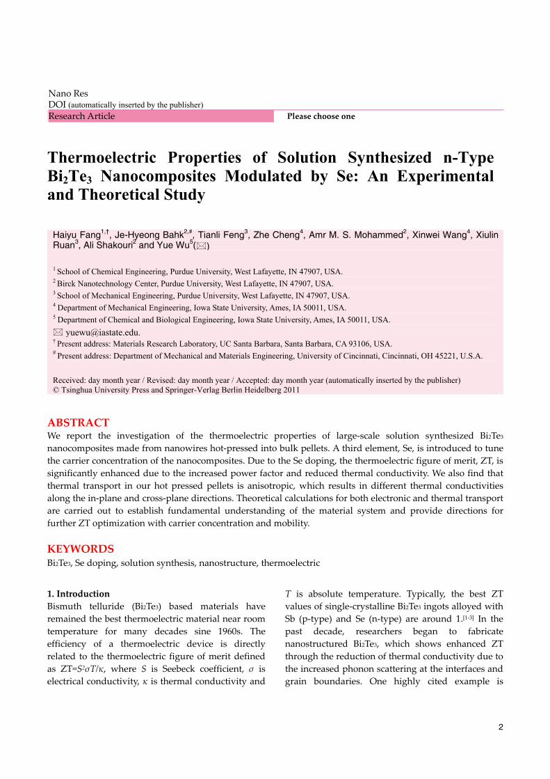
ABSTRACT We report the investigation of the thermoelectric properties of large-scale solution synthesized Bi2Te3
nanocomposites made from nanowires hot-pressed into bulk pellets. A third element, Se, is introduced to tune
the carrier concentration of the nanocomposites. Due to the Se doping, the thermoelectric figure of merit, ZT, is
significantly enhanced due to the increased power factor and reduced thermal conductivity. We also find that
thermal transport in our hot pressed pellets is anisotropic, which results in different thermal conductivities
along the in-plane and cross-plane directions. Theoretical calculations for both electronic and thermal transport
are carried out to establish fundamental understanding of the material system and provide directions for
further ZT optimization with carrier concentration and mobility.
KEYWORDS Bi2Te3, Se doping, solution synthesis, nanostructure, thermoelectric
1. Introduction
Bismuth telluride (Bi2Te3) based materials have
remained the best thermoelectric material near room
temperature for many decades sine 1960s. The
efficiency of a thermoelectric device is directly
related to the thermoelectric figure of merit defined
as ZT=S2σT/κ, where S is Seebeck coefficient, σ is
electrical conductivity, κ is thermal conductivity and
T is absolute temperature. Typically, the best ZT
values of single-crystalline Bi2Te3 ingots alloyed with
Sb (p-type) and Se (n-type) are around 1.[1-3] In the
past decade, researchers began to fabricate
nanostructured Bi2Te3, which shows enhanced ZT
through the reduction of thermal conductivity due to
the increased phonon scattering at the interfaces and
grain boundaries. One highly cited example is
Nano Res DOI (automatically inserted by the publisher) Research Article Please choose one

3
Bi0.5Sb1.5Te3 nanostructured bulk reached ZT of 1.4.[4]
This great success has since stimulated great deal of
research effort on nanostructured materials.
However, complex high-vacuum molecular beam
epitaxy and energy-intensive ball milling were
involved in fabricating those materials. Therefore,
solution synthesis of nanostructured Bi2Te3, as an
alternative path toward cost-effective and
energy-efficient material production, becomes very
attractive. R. J. Mehta et al. reported that solution
synthesized n-type Bi2Te3 and p-type Bi0.5Sb1.5Te3
nanoplates achieved ZT of 1.1 and 1.2 respectively,
which is the most successful effort so far in solution
synthesized nanostructured Bi2Te3.[5] However, the
scalability of solution synthesis was barely
demonstrated in the literature. Recently, our group
reported a 1 liter scale synthesis of Bi2Te3 nanowires,
in which over 17 gram of Bi2Te3 nanowires was
produced at an impressive yield of 94.21%,[6] which
provides enough nanopowder to make tens of pellets
through hot press. The scaled up reaction provides a
platform where the potential of thermoelectric
performance of solution-synthesized Bi2Te3 can be
thoroughly investigated by tuning various materials
parameters, such as carrier concentration, mobility
and so on, without repeating efforts invested to
synthesizing multiple batches. Meanwhile,
measuring samples from the same batch minimizes
the variation of materials properties among different
batches.
Bi2Te3 has a layered lattice structure and the
configuration of one quantum layer is
Te(1)-Bi-Te(2)-Bi-Te(1) (Fig. 1a). Te(1) and Bi are
covalently bonded while adjacent quantum layers
are loosely bonded thorough Van der Waals force.[7,8]
Due to the unique crystal structure, the defect
chemistry of Bi2Te3 is quite complicated. Te vacancy
is one of the most common defects existing in Bi2Te3.
Since Te (52.55 kJ/mol) has a smaller evaporation
energy than Bi (104.80 kJ/mol), Te tends to evaporate
more than Bi during high temperature consolidation
or annealing process.[9] Te vacancy can donate two
free electrons according to the following equation: 2 2Te TeTe V Te e , which significantly increases
n-type conductance.[10-12] Due to the small
electronegativity difference between Bi and Te,[13]
anti-site defects of Bi occupying Te site (BiTe) and Te
occupying Bi site (TeBi) are also widely found in
Bi2Te3. The formation of a BiTe antisite defect follows
this equation: Te TeBi Te Bi Te h and donates
one free hole to the matrix per site.[14-16] A TeBi antisite
defect, on the other hand, donates one free electron
to the matrix per site following the
equation: Bi BiTe Bi Te Bi e .[13,17] Recent
reports show that the Seebeck coefficient of Bi2Te3
nanowires is much lower than that of bulk mainly
due to higher carrier concentration contributed by
the antisite defects, which are more easily formed in
Bi2Te3 nanowire probably because of the dangling
bonds on the large surface area.[18-20] It is found that
the consolidated pellets of our large-scale
synthesized Bi2Te3 nanowires have extremely high
carrier concentrations, so Se was used as a dopant to
occupy double-charged Te vacancy and compensate
free electrons. Another important parameter that
often receives less attention is the carrier mobility in
nanostructured thermoelectric materials. The
theoretical work based on the experimental results
here reveals that mobility is just as important as
carrier concentration in designing thermoelectric
materials. Achieving the best ZT value depends on
the simultaneous optimization of carrier
concentration and mobility. Here, the combined
experimental and theoretical investigation provides a
thorough understanding of solution-synthesized
Bi2Te3 materials system.
Figure 1. (a) is a scheme of Bi2Te3 lattice; the picture is from

4
Jmol (an open-source Java viewer for chemical structures in 3D; http://www.jmol.org/). (b) is the XRD of as-synthesized Bi2Te3 nanowires. (c) is the low resolution TEM image of Bi2Te3 nanowires and (d) is the HRTEM image of one Bi2Te3 nanowire with the inset being the FFT of the selected area.
2. Results and Discussion
2.1. Materials characterization
The as-synthesized Bi2Te3 nanowires are
characterized by XRD and TEM (Fig. 1). The XRD
spectrum of the nanowires can be readily indexed as
Bi2Te3 (JCPDS No. 15-0863) without any impurity
peaks identified (Fig. 1b). The low resolution TEM
image shows the morphology of nanowires with
uniform distribution (Fig. 1c). The lattice resolved
image of a nanowire was obtained with high
resolution TEM (Fig. 1d), which reveals the
polycrystalline nature of a single nanowire while the
fast Fourier transformation is indexed as pure Bi2Te3
phase. More discussion on the Bi2Te3 nanowire
characterization can be found in our previous
report.[6]
Table 1. A summary of the relative density, Se atomic percentage and chemical formula of all the samples identified by numbers from 1 to 7.
Sample ID
Relative density (%)
Se atomic %
Bi2TexSey
1 92.42 0 Bi2Te2.62
2 92.81 1.52 ± 0.34 Bi2Te2.62Se0.07
3 92.49 3.91 ± 0.68 Bi2Te2.64Se0.19
4 90.57 5.66 ± 0.58 Bi2Te2.57Se0.27
5 90.44 8.20 ± 0.97 Bi2Te2.51Se0.4
6 91.95 11.54 ± 0.68
Bi2Te2.42Se0.58
7 91.34 17.71 ± 0.38
Bi2Te2.14Se0.89
Total 7 pellets with different Se concentrations were
fabricated for carrier concentration optimization.
First, the densities of Bi2Te3 nanocomposite pellets
with different Se concentrations were calculated
from the mass and the sample dimensions, and the
theoretical density of Bi2Te3 was used for the relative
density calculation. The results listed in Table 1
indicate that all of the pellets possess high relative
densities over 90%. Furthermore, Se concentration in
each pellet was measured with EDS, whose error
bars come from the geometrical distribution of Se
(Table 1). The corresponding chemical formula based
on the EDS results for each pellet is also summarized
in Table 1.
Figure 2. (a) is a summary of the XRD spectra of all 7 samples and the spikes are the standard spectrum of Bi2Te3 (JCPDS No. 15-0863). (b) shows the (0 0 6) peaks of the 7 samples. (c) and (d) are the change of calculated lattice constants a and c with Se atomic percentage, respectively.
Notably, the Se concentration has a significant
impact on the XRD spectra of the pellets as shown in
Fig. 2a. Generally speaking, Te and Se are in the
same group in the periodic table, but Se has a smaller
atomic radius than Te. Therefore, the Se doping
would decrease the lattice constants and cause the
XRD peaks shift to larger angles according to the
Bragg equation ( sin 2n d ). The initial
observation on the XRD spectra (Fig. 2a) confirms
this. Moreover, the calculated lattice constant a from
the XRD spectra show a decreasing trend with Se
concentration (Fig. 2c). However, the (0 0 6) peak
position (Fig. 2b), which is solely determined by the c
constant, first shift to a smaller angle and then to a
larger angle as Se content increases. The calculated
lattice constant c corresponds to the (0 0 6) peak
shifting and reaches the maximum value (30.229 Å)
that is, of course, still smaller than that of pure Bi2Te3
(30.483 Å) at the Se concentration of 3.91%.
Combining the EDS results (Table 1) and the fact that
a monotonically decreases while c first increases and

5
then decreases with Se concentration (Fig. 2d), we
propose a plausible Se doping mechanism that can
interpret the lattice constants as well as the carrier
concentration variation with Se concentration that
was measured later on.
Sample 1, which is made from pure Bi2Te3 nanowires
with no Se, is found to be Te deficient (Table 1),
which means lots of Te vacancies exist in the lattice.
As discussed earlier (Fig. 1a), since Bi2Te3 has a
layered lattice structure, the existence of a large
number of Te vacancies implies that some Te atomic
layers are missing in the lattice, which leads to a
smaller c constant (29.891 Å) than that of
perfect-crystal Bi2Te3 (30.483 Å), whereas the a
constant (4.409 Å) is slightly higher than that of
perfect-crystal Bi2Te3 (4.385 Å) because Bi has a larger
atomic radius than Te. When Se is doped into the
Bi2Te3 pellets, Te vacancies are occupied by Se so that
the layer structure is stretched along the c direction,
leading to a larger c constant. However, the a
constant becomes smaller because Se has a much
shorter atomic radius than Bi and Te. As Se
concentration continues to increase after 3.91%, the c
constant starts to decrease while a constant keeps
going down. At this point, Se not only fills the Te
vacancies but also starts occupying the Bi atomic
layers to form SeBi antisites or even replacing Te,
probably because of the defect formation energy of
SeBi antisites becomes favorable with richer Se or
poorer Bi.[13] Again, due to the atomic radius
difference between Bi and Se, the layer structure
shrinks in c direction, leading to a decreasing c
constant, while a constant keeps its decreasing trend.
Figure 3. Influence of Se concentration on thermoelectric properties at 300 K. (a) Carrier concentration; (b) the theoretical calculation result of band gap and effective mass; (c) Mobility; (d) Seebeck coefficient and electrical conductivity; (e) Pisarenko relation (Seebeck coefficient vs. carrier concentration); (f) power factor.
2.2. Electrical Properties with Varying Se
Concentration
Figure 3 shows how Se concentration influences the
electrical properties of the samples at 300 K. As
discussed earlier, each Te vacancy donates two
electrons, so Sample 1 with no Se has an extremely
high carrier concentration of 5.36×1020 cm-3 (Fig. 3a).
When Se was doped into the system, Sample 2 and 3
possess reduced carrier concentration because Se
occupies the Te vacancy and compensates the two
free electrons:2 2Te TeSe V e Se , which
decreases carrier concentration in the material. The
Se doping efficiency is calculated to be 0.45 electrons
per Se atom from the results of Sample 1 – 3.
Interestingly, the carrier concentration reaches a
minimum value of 2.84×1019 cm-3 in Sample 3 with 3.9
% Se and then starts to increase, which exactly
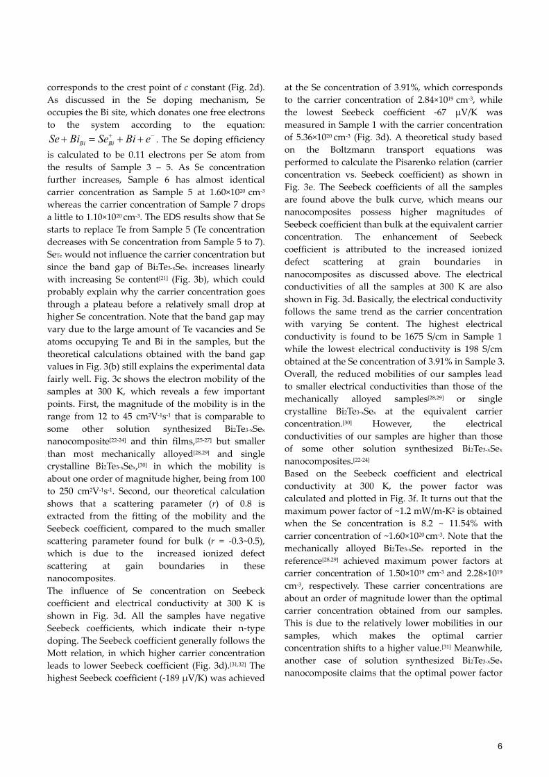
6
corresponds to the crest point of c constant (Fig. 2d).
As discussed in the Se doping mechanism, Se
occupies the Bi site, which donates one free electrons
to the system according to the equation:
Bi BiSe Bi Se Bi e . The Se doping efficiency
is calculated to be 0.11 electrons per Se atom from
the results of Sample 3 – 5. As Se concentration
further increases, Sample 6 has almost identical
carrier concentration as Sample 5 at 1.60×1020 cm-3
whereas the carrier concentration of Sample 7 drops
a little to 1.10×1020 cm-3. The EDS results show that Se
starts to replace Te from Sample 5 (Te concentration
decreases with Se concentration from Sample 5 to 7).
SeTe would not influence the carrier concentration but
since the band gap of Bi2Te3-xSex increases linearly
with increasing Se content[21] (Fig. 3b), which could
probably explain why the carrier concentration goes
through a plateau before a relatively small drop at
higher Se concentration. Note that the band gap may
vary due to the large amount of Te vacancies and Se
atoms occupying Te and Bi in the samples, but the
theoretical calculations obtained with the band gap
values in Fig. 3(b) still explains the experimental data
fairly well. Fig. 3c shows the electron mobility of the
samples at 300 K, which reveals a few important
points. First, the magnitude of the mobility is in the
range from 12 to 45 cm2V-1s-1 that is comparable to
some other solution synthesized Bi2Te3-xSex
nanocomposite[22-24] and thin films,[25-27] but smaller
than most mechanically alloyed[28,29] and single
crystalline Bi2Te3-xSex,[30] in which the mobility is
about one order of magnitude higher, being from 100
to 250 cm2V-1s-1. Second, our theoretical calculation
shows that a scattering parameter (r) of 0.8 is
extracted from the fitting of the mobility and the
Seebeck coefficient, compared to the much smaller
scattering parameter found for bulk (r = -0.3~0.5),
which is due to the increased ionized defect
scattering at gain boundaries in these
nanocomposites.
The influence of Se concentration on Seebeck
coefficient and electrical conductivity at 300 K is
shown in Fig. 3d. All the samples have negative
Seebeck coefficients, which indicate their n-type
doping. The Seebeck coefficient generally follows the
Mott relation, in which higher carrier concentration
leads to lower Seebeck coefficient (Fig. 3d).[31,32] The
highest Seebeck coefficient (-189 μV/K) was achieved
at the Se concentration of 3.91%, which corresponds
to the carrier concentration of 2.84×1019 cm-3, while
the lowest Seebeck coefficient -67 μV/K was
measured in Sample 1 with the carrier concentration
of 5.36×1020 cm-3 (Fig. 3d). A theoretical study based
on the Boltzmann transport equations was
performed to calculate the Pisarenko relation (carrier
concentration vs. Seebeck coefficient) as shown in
Fig. 3e. The Seebeck coefficients of all the samples
are found above the bulk curve, which means our
nanocomposites possess higher magnitudes of
Seebeck coefficient than bulk at the equivalent carrier
concentration. The enhancement of Seebeck
coefficient is attributed to the increased ionized
defect scattering at grain boundaries in
nanocomposites as discussed above. The electrical
conductivities of all the samples at 300 K are also
shown in Fig. 3d. Basically, the electrical conductivity
follows the same trend as the carrier concentration
with varying Se content. The highest electrical
conductivity is found to be 1675 S/cm in Sample 1
while the lowest electrical conductivity is 198 S/cm
obtained at the Se concentration of 3.91% in Sample 3.
Overall, the reduced mobilities of our samples lead
to smaller electrical conductivities than those of the
mechanically alloyed samples[28,29] or single
crystalline Bi2Te3-xSex at the equivalent carrier
concentration.[30] However, the electrical
conductivities of our samples are higher than those
of some other solution synthesized Bi2Te3-xSex
nanocomposites.[22-24]
Based on the Seebeck coefficient and electrical
conductivity at 300 K, the power factor was
calculated and plotted in Fig. 3f. It turns out that the
maximum power factor of ~1.2 mW/m-K2 is obtained
when the Se concentration is 8.2 ~ 11.54% with
carrier concentration of ~1.60×1020 cm-3. Note that the
mechanically alloyed Bi2Te3-xSex reported in the
reference[28,29] achieved maximum power factors at
carrier concentration of 1.50×1019 cm-3 and 2.28×10¹⁹
cm-3, respectively. These carrier concentrations are
about an order of magnitude lower than the optimal
carrier concentration obtained from our samples.
This is due to the relatively lower mobilities in our
samples, which makes the optimal carrier
concentration shifts to a higher value.[31] Meanwhile,
another case of solution synthesized Bi2Te3-xSex
nanocomposite claims that the optimal power factor

7
was obtained at a much higher carrier concentration
of 7.8×1020 cm-3 and the corresponding mobility was
1.33 cm2V-1s-1.[24]
Figure 4. The temperature dependent thermoelectric properties. (a) electrical conductivity; (b) Seebeck coefficient; (c) power factor.
Figure 4 shows the temperature dependent
thermoelectric properties of the Bi2Te3-xSex
nanocomposites. On one hand, the negative
temperature dependent behavior of electrical
conductivity of almost all the samples indicates they
are degenerate semiconductors except for Sample 3,
which shows a positive temperature coefficient
(dσ/dT) due to its low carrier concentration (Fig. 4a).
We also note that the peak Seebeck coefficient shifts
from 480 K in Sample 1 to 400 – 440 K in other
samples because the reduced carrier concentration
by Se doping decreases the onset temperature of
bipolar effect (Fig. 4b).[33] The power factor is plotted
in Fig. 4c. Due to the decreasing Seebeck coefficient
with temperature, Sample 3 has the lowest power
factor among the samples. Also, in the temperature
range of 300 – 500 K, the optimal Se concentration is
11.54% which gives the highest power factor of 1.48
mW/m-K2 at 400 K. This value is much higher than
that of the pure Bi2Te3 (no Se) nanocomposite (1.04
mW/m-K2 at 400 K and 1.16 mW/m-K2 at 480 K). The
enhancement is attributed to the optimized carrier
concentration and increased mobility.
2.3. Anisotropic Thermal Conductivity and ZT
In order to investigate the anisotropy in thermal
conductivity, which is expected due to the highly
anisotropic lattice structure of Bi2Te3-xSex (Fig. 1a), the
thermal conductivity was measured along two
different directions, in-plane and cross-plane at 300
K. The measurement results (Fig. 5a) show that the
in-plane thermal conductivity is around two times
higher than the cross-plane thermal conductivity.
The Scanning Electron Microscope (SEM) images at
the pellets cross section reveal the laminated
structure after hot press, which explains the
anisotropic thermal transport in the support
information (Fig. S-1). The anisotropic thermal
transport is thought to be caused by the hot press
process, because the set-up used in this research has
a slow ramping speed (~5 degree per minute) and an
even slower cooling speed (~1 degree per minute),
which significantly extended the time when the
samples were kept at high temperature, leading to
the regrowth of Bi2Te3 crystals. The regrown crystals
preferably form laminates stacking in the direction
where the pressure was applied, which is the
cross-plane direction of the pellets. As Bi2Te3 has a
layered lattice structure, the cross-plane direction of
the laminate-like crystals in the pellets may be along
the c axis, where the thermal conductivity of Bi2Te3 is
the smallest since the quantum layers are connected
with Van der Waals force (Fig. 1a). Therefore, a much
smaller thermal conductivity is observed in the
cross-plane direction than the in-plane direction of
the pellets. To minimize the regrowth, spark plasma
sintering is more preferred, since it has a fast
ramping and cooling speed which assures the
samples do not stay at high temperature for too long
while making dense pellets.[34] Another interesting
aspect is that the thermal conductivity decreased
significantly with increasing Se content, which is
mainly due to the reduced electronic thermal
conductivity. The electronic and lattice contribution
to the in-plane thermal conductivity are also
calculated and plotted in Fig. 5a. The lattice thermal
conductivity first increases and then decreases with

8
Se concentration, which could be caused by the
defects in the samples. In Sample 1, there are lots of
Te vacancies and these defects are compensated by
Se occupation after Se doping, so from Sample 1 to 3,
the lattice thermal conductivity increases with Se
concentration. However, after Sample 3, the new
defects, SeTe antisites, start to form and potentially
reduce the lattice thermal conductivity. The
temperature dependent cross-plane thermal
conductivity can be found in Fig. S-2. The
temperature dependent in-plane thermal
conductivity was not measured because of
instrumental limitation. Since the electrical
properties were measured at in-plane direction, the
in-plane thermal conductivity was used to calculate
ZT, shown in Fig. 5b. The ZT is enhanced via Se
doping by a factor of three and peaks at Se
concentration of ~ 11 %. The increase in power factor
and reduction in thermal conductivity from Se
doping both contribute to the ZT improvement.
Figure 5. (a) shows the in-plane and cross-plane thermal conductivity at different Se concentration; the in-plane electronic and lattice contribution are also plotted. (b) is ZT at different Se concentration using in-plane properties. The properties were measured at 300 K.
2.4. Further ZT Optimization with Theoretical
Modelling
One of the important material parameters that limit
ZT in our nanocomposites is the low mobility.
Reduced mobility in nanostructured materials is not
unusual; it is found in other solution-synthesized
nanostructured n-type Bi2Te3.[22-24] Thus, here we
performed a theoretical study to investigate the
impact of mobility enhancement on the figure of
merit at a given carrier concentration in Bi2Te2.5Se0.5.
Three different carrier concentrations, i.e. 2×1019 cm-3,
9×1019 cm-3 and 1.6×1020 cm-3, were considered for this
study, and the mobility was varied by reducing the
carrier scattering strength at each carrier
concentration. The results of the calculated transport
properties as a function of mobility are shown in Fig.
6. We scanned the mobility from the measured
value in our samples up to the bulk value at each
carrier concentration.
As shown in Fig. 6b, the power factor increases
rapidly with mobility due to the improved electrical
conductivity (Fig. 6a). and then rolls over as the
mobility further increases due to the reduced
Seebeck coefficient (Fig. 6a) as shown for the carrier
concentration of 9×1019 cm-3. In general, at low
mobility side, higher carrier concentration leads to
better power factor; however at high mobility side,
lower carrier concentration results in better power
factor (Fig. 6b).
Thermal conductivity typically consists of electronic,
lattice and bipolar contributions, with the last
component being negligible at room temperature for
Bi2Te3.[35] The electronic contribution of thermal
conductivity e was calculated using the
Wiedemann-Franz relation with the Lorenz number
(L) of 2.44×10⁻⁸ WΩ/K2. The lattice thermal
conductivity l as a function of mobility was
obtained by assuming that the mobility is tuned by
grain size, e.g. electron grain boundary scattering
(Support Information). The estimated grain diameter
for sample 5 and 6 is around 4.35 nm, which is larger
than the effective phonon mean free path ~2.4 nm
but much smaller than the effective electron mean
free path ~24 nm in bulk 10% Se Bi2Te3 with carrier
concentration of 1.6×1020 cm-3 (Support information).
As a consequence, the lattice thermal conductivity
does not increase as significantly as electronic
thermal conductivity with mobility, as shown in Fig.
6c. The increases of the lattice and the electronic
thermal conductivities are around 50% and 350%
from the sample nanostructure to the corresponding
bulk for the carrier concentration of 1.6×1020 cm-3. As
a result, the electronic thermal conductivity is
responsible for major portion of the total thermal
conductivity at high mobility.
Nanostructuring benefits ZT in these
nanocomposites only when the lattice contributes a
small portion to the total thermal conductivity. The
effect of nanostructuring can be understood
explicitly from the ZT expression
of2 / ( / )lS T LT , where
2S increases
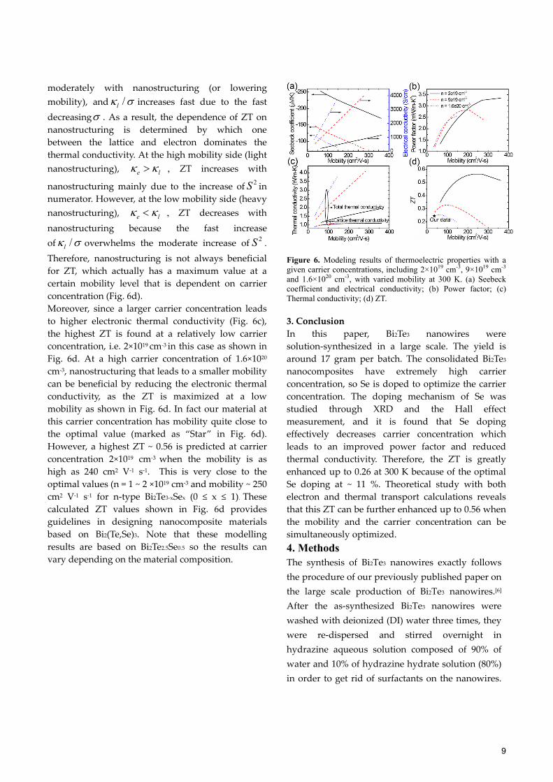
9
moderately with nanostructuring (or lowering
mobility), and /l increases fast due to the fast
decreasing . As a result, the dependence of ZT on
nanostructuring is determined by which one
between the lattice and electron dominates the
thermal conductivity. At the high mobility side (light
nanostructuring), e l , ZT increases with
nanostructuring mainly due to the increase of2S in
numerator. However, at the low mobility side (heavy
nanostructuring), e l , ZT decreases with
nanostructuring because the fast increase
of /l overwhelms the moderate increase of2S .
Therefore, nanostructuring is not always beneficial
for ZT, which actually has a maximum value at a
certain mobility level that is dependent on carrier
concentration (Fig. 6d).
Moreover, since a larger carrier concentration leads
to higher electronic thermal conductivity (Fig. 6c),
the highest ZT is found at a relatively low carrier
concentration, i.e. 2×1019 cm-3 in this case as shown in
Fig. 6d. At a high carrier concentration of 1.6×10²⁰
cm-3, nanostructuring that leads to a smaller mobility
can be beneficial by reducing the electronic thermal
conductivity, as the ZT is maximized at a low
mobility as shown in Fig. 6d. In fact our material at
this carrier concentration has mobility quite close to
the optimal value (marked as “Star” in Fig. 6d).
However, a highest ZT ~ 0.56 is predicted at carrier
concentration 2×1019 cm-3 when the mobility is as
high as 240 cm2 V-1 s-1. This is very close to the
optimal values (n = 1 ~ 2 ×1019 cm-3 and mobility ~ 250
cm2 V-1 s-1 for n-type Bi2Te3-xSex (0 ≤ x ≤ 1). These
calculated ZT values shown in Fig. 6d provides
guidelines in designing nanocomposite materials
based on Bi2(Te,Se)3. Note that these modelling
results are based on Bi2Te2.5Se0.5 so the results can
vary depending on the material composition.
Figure 6. Modeling results of thermoelectric properties with a given carrier concentrations, including 2×1019 cm-3, 9×1019 cm-3 and 1.6×1020 cm-3, with varied mobility at 300 K. (a) Seebeck coefficient and electrical conductivity; (b) Power factor; (c) Thermal conductivity; (d) ZT.
3. Conclusion
In this paper, Bi2Te3 nanowires were
solution-synthesized in a large scale. The yield is
around 17 gram per batch. The consolidated Bi2Te3
nanocomposites have extremely high carrier
concentration, so Se is doped to optimize the carrier
concentration. The doping mechanism of Se was
studied through XRD and the Hall effect
measurement, and it is found that Se doping
effectively decreases carrier concentration which
leads to an improved power factor and reduced
thermal conductivity. Therefore, the ZT is greatly
enhanced up to 0.26 at 300 K because of the optimal
Se doping at ~ 11 %. Theoretical study with both
electron and thermal transport calculations reveals
that this ZT can be further enhanced up to 0.56 when
the mobility and the carrier concentration can be
simultaneously optimized.
4. Methods The synthesis of Bi2Te3 nanowires exactly follows
the procedure of our previously published paper on
the large scale production of Bi2Te3 nanowires.[6]
After the as-synthesized Bi2Te3 nanowires were
washed with deionized (DI) water three times, they
were re-dispersed and stirred overnight in
hydrazine aqueous solution composed of 90% of
water and 10% of hydrazine hydrate solution (80%)
in order to get rid of surfactants on the nanowires.
10
Then, the Bi2Te3 nanowires were washed with 3
times with DI water and 1 time with ethanol before
dried completely in vacuum and annealed at 450 °C
for half an hour. Afterwards, the Bi2Te3 nanowires
lumps were ground into fine power in a glovebox
with nitrogen protection and then Se powder was
thoroughly mixed with the nanowires by grinding.
Finally, the mixture was consolidated into
centimeter pellets with hot press at 450 °C for half
an hour.
Acknowledgements
H. F. thanks Scott Finefrock and Tianyue Gao for the
help in Hall measurement. H. F. and Y. W.
acknowledge the use of the hot press setup in Prof.
Chin-The Sun’s lab at Purdue University. H. F. and Y.
W. acknowledge Air Force Office of Scientific
Research (Award Number FA9550-12-1-0061). T. F.
and X. R. acknowledge the partial support from
National Science Foundation (Award No. 1150948).
Electronic Supplementary Material: Supplementary
material (details of experiments and procedures for
the theoretical, SEM images of the cross section of
hot pressed pellets, temperature dependent cross
section thermal conductivity and schematic of the
experimental setup for characterizing the in-plane
thermal conductivity) is available in the online
version of this article at
http://dx.doi.org/10.1007/s12274-***-****-*
(automatically inserted by the publisher). References [1] Yim, W. M.; Rosi, F. D. Solid-State Electron. 1972, 15,
1121. [2] Carle, M.; Pierrat, P.; Lahallegravier, C.; Scherrer, S.;
Scherrer, H. J. Phys. Chem. Solids 1995, 56, 201. [3] Yamashita, A.; Tomiyoshi, S.; Makita, K. J. Appl. Phys.
2003, 93, 368. [4] Poudel, B.; Hao, Q.; Ma, Y.; Lan, Y.; Minnich, A.; Yu, B.;
Yan, X.; Wang, D.; Muto, A.; Vashaee, D.; Chen, X.; Liu, J.; Dresselhaus, M.; Chen. G.; Ren, Z. Science 2008, 320, 634.
[5] Mehta, R.; Zhang, Y. L.; Karthik, C.; Singh, B.; Siegel, R. W.; Borca-Tasciuc, T.; Ramanath, G. Nature Mater. 2012, 11, 233.
[6] Finefrock, S. W.; Fang, H.; Yang, H.; Darsono H.; Wu, Y. Nanoscale 2014, 6, 7872.
[7] Drabble J. R.; Goodman, C. H. L. J. Phys. Chem. Solids 1958, 5, 142.
[8] Mishra, S. K.; Satpathy, S.; Jepsen, O. J. Phys.: Condens. Matter. 1997, 9, 461.
[9] Liu, W. S.; Zhang, Q.; Lan, Y.; Chen, S.; Yan, X.; Zhang, Q.; Wang, H.; Wang, D.; Chen, G.; Ren, Z. Adv. Energy Mater. 2011, 1, 577.
[10] Schultz, J. M.; McHugh, J. P.; Tiller, W. A. J.Appl. Phys. 1962, 33, 2443.
[11] D. B. Hyun, J. S. Hwang, J. D. Shim, and T. Oh, J. Mater. Sci. 2001, 36, 1285.
[12] Jiang, J.; Chen, L.; Bai, S.; Yao, Q.; Wang, Q. Mater. Sci. Eng.: B 2005, 117, 334.
[13] Scanlon, D. O.; King, P. D. C.; Singh, R. P.; de la Torre, A.; Walker, S. M.; Balakrishnan, G.; Baumberger, F.; Catlow, C. R. A. Adv. Mater. 2012, 24, 2154.
[14] Starý, Z.; Horák, J.; Stordeur, M.; Stölzer, M. J. Phys. Chem. Solids 1988, 49, 29.
[15] Jia, S.; Ji, H.; Climent-Pascual, E.; Fuccillo, M. K.; Charles, M. E.; Xiong, J.; Ong, N. P.; Cava, R. J. Phys. Rev. B 2011, 84, 235206.
[16] Fuccillo, M. K.; Jia, S.; Charles, M. E.; Cava, R. J. J. Electron. Mater. 2013, 42, 1246.
[17] Jia, S.; Beidenkopf, H.; Drozdov, I.; Fuccillo, M. K.; Seo, J.; Xiong, J.; Ong, N. P.; Yazdani, A.; Cava, R. J. Phys. Rev. B 2012, 86, 165119.
[18] Mavrokefalos, A.; Moore, A. L.; Pettes, M. T.; Shi, L.; Wang, W.; Li, X. J. Appl. Phys. 2009, 105, 104318.
[19] Chen, B. L.; Chen, Y. Y.; Lin, S. J.; Ho, J. C.; Lee, P. C.; Chen, C. D.; Harutyunyan, S. R. J. Phys. Chem. C 2010, 114, 3385.
[20] Shin, H. S.; Jeon, S. G.; Yu, J.; Kim, Y. S.; Park, H. M.; Song, J. Y. Nanoscale 2014, 6, 6158.
[21] Neuberger, M. The BiTe-BiSe system data sheet, Airforce Mater. Res. Lab (1966).
[22] Son, J. S.; Choi, M. K.; Han, M. K.; Park, K.; Kim, J. Y.; Lim, S. J.; Oh, M.; Kuk, Y.; Park, C.; Kim, S. J.; Hyeon, T. Nano Lett. 2012, 12, 640.
[23] Zhao, Y.; Dyck, J. S.; Hernandez, B. M.; Burda, C. J. Phys. Chem. C 2010, 114, 11607.
[24] Soni, A.; Yanyuan, Z.; Ligen, Y.; Aik, M. K. K.; Dresselhaus, M. S.; Xiong, Q. Nano Lett. 2012, 12, 1203.
[25] Yoo, B. Y.; Huang, C. K.; Lim, J. R.; Herman, J.; Ryan, M. A.; Fleurial, J. P.; Myung, N. V. Electrochim. Acta 2005, 50, 4371.
[26] Kim, D. H.; Byon, E.; Lee, G. H.; Cho, S. Thin Solid Films 2006, 510, 148.
[27] Boulouz, A.; Giani, A.; Pascal-Delannoy, F.; Boulouz, M.; Foucaran, A.; Boyer, A. J. Cryst. Growth 1998, 194, 336b.
[28] Yang, J. Y.; Aizawa, T.; Yamamoto, A.; Ohta, T. J. Alloys Compd. 2000, 312, 326.
[29] Liu, W. S.; Zhang, Q.; Lan, Y.; Chen, S.; Yan, X.; Zhang,
11
Q.; Wang, H.; Wang, D.; Chen, G.; Ren, Z. Adv. Energy Mater. 2011, 1, 577.
[30] Carle, M.; Pierrat, P.; Lahallegravier, C.; Scherrer, S.; Scherrer, H. J. Phys. Chem. Solids 1995, 56, 201.
[31] Goldsmid, J. H. Introduction to Themoelectricity, Springer, New York, USA 2010.
[32] Cutler, M.; Mott, N. F. Phys. Rev. 1969, 181, 1336.
[33] Rowe, D. M.; Bhandari, C. M. Modern Thermoelectrics, Reston Publishing Company, INC., Reston, Virginia, USA, 1983.
[34] Fang, H.; Wu, Y. J. Mater. Chem. A 2014, 2, 6004 [35] Fang, H.; Feng, T.; Yang, H.; Ruan, X.; Wu, Y. Nano Lett.
2013, 13, 2058.

12
Electronic Supplementary Material
Thermoelectric Properties of Solution Synthesized n-Type Bi2Te3 Nanocomposites Modulated by Se: An Experimental and Theoretical Study
Haiyu Fang1,†, Je-Hyeong Bahk2,#, Tianli Feng3, Zhe Cheng4, Amr M. S. Mohammed2, Xinwei Wang4, Xiulin Ruan3, Ali Shakouri2 and Yue Wu5() 1 School of Chemical Engineering, Purdue University, West Lafayette, IN 47907, USA. 2 Birck Nanotechnology Center, Purdue University, West Lafayette, IN 47907, USA. 3 School of Mechanical Engineering, Purdue University, West Lafayette, IN 47907, USA. 4
Department of Mechanical Engineering, Iowa State University, Ames, IA 50011, USA. 5
Department of Chemical and Biological Engineering, Iowa State University, Ames, IA 50011, USA.
[email protected]. † Present address: Materials Research Laboratory, UC Santa Barbara, Santa Barbara, CA 93106, USA. # Present address: Department of Mechanical and Materials Engineering, University of Cincinnati, Cincinnati, OH 45221, U.S.A.
Received: day month year / Revised: day month year / Accepted: day month year (automatically inserted by the publisher) © Tsinghua University Press and Springer-Verlag Berlin Heidelberg 2011
1. Measurement of thermoelectric properties:
1.1. Cross-plane thermal conductivity measurement. The pellets were cut and polished into required
dimensions. Seebeck coefficient was measured in home built system by bridging the sample between a
heater and heat sink and testing the voltage and temperature difference between the hot and the cold sides in
a vacuum chamber. Electrical conductivity was measured with Van der Pauw method in a system where a
MMR K-20 temperature stage was used to control sample temperature and an Agilent was connected to
provide source current and collect voltage signals. Hall Effect was carried out by applying magnetic field up
to 1 Tesla to the electrical conductivity measurement system. The cross-plane thermal conductivity was
calculated via the equation κ = αρCp (ρ is the density and Cp is heat capacity) and the thermal diffusivity (α)
was measured through the laser flush method. All the measurements were carried out under vacuum in the
temperature range from 300 to 500 K.
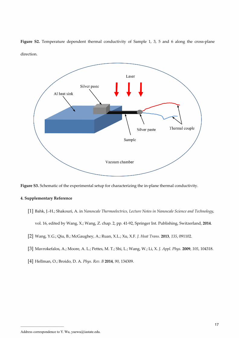
1.2 In-plane thermal conductivity measurement. The schematic of the experimental setup for characterizing
the in-plane thermal conductivity is shown in Figure S3. The sample was fixed on the aluminum heat sink
with silver paste that was also used to connect the thermal couple to the suspended end of the sample. To
suppress heat convection, the setup was placed in a vacuum chamber with pressure of 2.1-2.3 mTorr. A 1550
nm laser was used to heat the sample. To enhance laser energy absorption, a black marker was used to
paint the sample surface facing the laser. Two lenses were used to enlarge the laser spot before the laser
entered the vacuum chamber. Since the laser spot is much larger than the sample size, the laser energy flux
hit on the sample surface can be taken as uniform. The heat sink was at room temperature. After laser was
applied, the temperature of the suspended sample end rose and it was measured by the thermal couple. The
13
temperature rise is related to the sample’s thermal conductivity as (2 )T Ql wd . Here, Q is the
heating energy, l is the sample length, κ is the thermal conductivity, w and d are the width and thickness
respectively. Then the thermal conductivity can be expressed as (2 )Ql Twd . To measure the heating
energy, a piece of hard and thick paper was placed at the position of the sample. The paper was used to
block the laser and a hole sharing the same size of the sample was cut in the paper. The light passed through
the hole and a laser power meter (POWER MAX500D) was placed underneath the paper to measure the laser
energy. The sample length, width and thickness were measured with micrometer and optical microscope.
Then the thermal conductivity of the sample was calculated. The calculated thermal conductivity includes
the effect of thermal radiation. The effect of radiation can be calculated as 3 2 28 ( )rad T l d . Here,
is the emissivity, is Stefan-Boltzmann constant, T is the surface temperature. For the emissivity, the
value for the surface facing the laser is 1 and the value for the other surface is estimated to be 0.5, so the
average emissivity of the sample is estimated to be 0.75. The maximum effect of radiation is very small
(about 3%) so that it would not bring significant error to the final results. The real thermal conductivity of the
sample is real rad . To improve the accuracy, one sample was measured for four times with different
laser energy and temperature rises. The main error source in this experiment is the laser energy absorption
rate, namely the emissivity. The sample surface is coarse and black so the emissivity is taken as 1 in this
experiment. The error due to the emissivity is estimated to be 5%. The relative error of the geometrical
measurement is estimated to be 1% and the relative error of the thermal couple is also 1%. Therefore, the
total relative error of the thermal conductivity is estimated to be 5.4%.
2. Theoretical modeling
2.1. Carrier transport modeling. We modeled the carrier transport in the Bi2(Te1-xSex)3 nanocomposites based
on the linearized Boltzmann transport equations (BTE) under the relaxation time approximation. The
differential conductivity σd(E) is defined as
E
fEEvEeE DOSd
022 )()()()( , (S1)
where e is the electron charge, τ is the total relaxation time, ρDOS is the density of states, v is the carrier
velocity in one direction, and f0 is the Fermi-Dirac distribution. For the multiple-band transports in
Bi2(Te1-xSex)3, the transport properties are calculated by summing all the contributions from each band. The
electrical conductivity σ, the Seebeck coefficient S, and the electronic thermal conductivity e are given,
respectively, by
dEEd , (S2)
dEEEE
qTS
Fd )( 1, (S3)

14
TLe , (S4)
where Σ is sum over the bands, q is −e for conduction bands, and +e for valence bands, T is the absolute
temperature, and EF is the relative position of the Fermi level to each of the band edge. In fact, the Lorenz
number is a function of the Fermi level and band structure, but we found that all the samples in this paper
were highly degenerate, so that the Lorenz number can be assumed to be the conventional value, 2.44 × 10⁻⁸
W Ω-1 K-2. More information about the electron transport modeling is found elsewhere.[1]
We included two major conduction bands and two valence bands in our transport modeling, all of which
are modeled as non-parabolic bands with 6 band degeneracy each. The band gap, effective masses are all
dependent on the Se content, x, found from literature, but assumed to be temperature-independent in this
paper. The relaxation time is determined by several major scattering mechanisms in Bi2(Te1-xSex)3. Acoustic
phonon deformation potential scattering is a major scattering mechanism for electrons in bulk. In the
nanocomposites, we added intense ionized defect scatterings at grain boundaries with the defect density as a
fitting parameter to fit the mobility.
2.2. Lattice thermal conductivity modeling. The calculation of lattice thermal conductivity as a function of
electron mobility consists of two steps. The first step is to figure out the average grain diameter for a given
electron mobility by using electron grain boundary scattering. The second step is to estimate the thermal
conductivity according to the average grain diameter and the phonon-boundary scattering.
2.2.1. Calculate the average grain diameter. The electron mobility and the grain diameter D in the
nanocomposites are related by the electron scattering with the Matthiessen’s rule
*
1 1 1 1 1
1 1
1 = ,
imp def latt bound
bulk bound
F
bulk
m v
eD
(S5)
where 1/ imp , 1/ def , 1/ latt , etc., represent electron impurity scattering, electron defect
scattering, electron phonon (lattice) scattering, etc., in bulk Bi2Te3 with 10% Se. The summation of them gives
the reciprocal mobility 1/ bulk in the bulk Bi2Te3 with 10% Se. The last term 1/ bound represents the
electron boundary scattering in nanostructured Bi2Te3 with 10% Se, which is determined
by* *bound
F
e e D
m m v . Here
*m and Fv are the effective electron mass and the Fermi velocities of
electrons, respectively. Based on Eq. S5, the average grain diameter D for a given electron mobility is
1 *1 1.F
bulk
mD v
e
(S6)
15
For the three carrier concentrations, i.e. 2×1019 cm-3, 9×1019 cm-3 and 1.6×1020 cm-3, the bulk mobilities
bulk are 320 cm2/V-s, 250 cm2/V-s and 220 cm2/V-s, and the Fermi velocities Fv are estimated as 1.5×10⁵
m/s, 2.2×10⁵ m/s and 2.7×10⁵ m/s, respectively. The effective electron mass is *
00.7m m , with 0m
representing the electron static mass. Based on Eq. S6, the average grain diameter of Sample 5 and 6 are
estimated around 4.35 nm. Such grain size reduces the electron mean free path
*F bulk
e F bulk
v mv
e
(24
nm) in bulk Bi2Te3 with 10% Se and carrier concentration of 1.6×1020 cm-3 to 3.7 nm in nanostructured Bi2Te3
with 10% Se (e.g. Sample 5 and 6).
2.2.2. Calculate the lattice thermal conductivity. Similar to electron transport, the effective phonon mean
free path p in nanocomposites is determined by phonon scattering in bulk and phonon-boundary
scattering in nano-grains,
,
1 1 1.
p p bulk D
(S7)
Based on kinetic theory, the lattice thermal conductivity is max
,0
1( ) ( ) ( )
3l g p sp pc v d
,
where is defined as max
0
1( ) ( )
3 gc v d
with ,c, gv and ,p sp representing the phonon
frequency, specific heat, group velocity and spectral mean free path, respectively. Based on our previous
calculation[2] and the literature,[3,4] is estimated as 5.767×10⁸ W/m2-K. Multiplying Eq. S7 by gives the
grain diameter dependent lattice thermal conductivity of nanocoposites
,
1 1 1
l l bulk D
. (S8)
Here the unknown ,l bulk represents the lattice thermal conductivity of bulk Bi2Te3 with 10% Se and is
obtained in the following approach. Sample 5 and 6 have the electrical conductivities of 907 S/cm and 829
S/cm, and thus electronic thermal conductivities e L T of 0.664 W/m-K and 0.607 W/m-K respectively.
Their in-plane thermal conductivities were measured as 1.63 W/m-K and 1.42 W/m-K, respectively. Thus
their lattice thermal conductivities are estimated as 0.966 W/m-K and 0.813 W/m-K, respectively. Sample 5
has a bit larger lattice thermal conductivity is owing to its lower Se concentration and thus less phonon
impurity scattering. Since the Se concentration of 10% in our modeling is very close and in between our
samples 5 (8.20 ± 0.97 % Se) and 6 (11.54 ± 0.68% Se), and the grain diameters of Sample 5 and 6 are both
around 4.35 nm, thus, the lattice thermal conductivity of our modeling material, i.e. Se concentration of 10%,
with grain diameter of 4.35 nm is estimated as l =0.89 W/m-K, the average of 0.966 W/m-K and 0.813

16
W/m-K. Finally ,l bulk is obtained as
1
,
1 1l bulk
l D
1.38 W/m-K. Since both the constants ,l bulk
and have been obtained, the lattice thermal conductivity as a function of grain diameter D, or electron
mobility , can be calculated based on Eq. S8.
3. Supplementary Figures
Figure S1. Scanning electron microscope images at the cross section of hot press pellets. Sample ID is
labeled on the images.
17
Figure S2. Temperature dependent thermal conductivity of Sample 1, 3, 5 and 6 along the cross-plane
direction.
Figure S3. Schematic of the experimental setup for characterizing the in-plane thermal conductivity.
4. Supplementary Reference
[1] Bahk, J.-H.; Shakouri, A. in Nanoscale Thermoelectrics, Lecture Notes in Nanoscale Science and Technology,
vol. 16, edited by Wang, X.; Wang, Z. chap. 2, pp. 41-92, Springer Int. Publishing, Switzerland, 2014.
[2] Wang, Y.G.; Qiu, B.; McGaughey, A.; Ruan, X.L.; Xu, X.F. J. Heat Trans. 2013, 135, 091102.
[3] Mavrokefalos, A.; Moore, A. L.; Pettes, M. T.; Shi, L.; Wang, W.; Li, X. J. Appl. Phys. 2009, 105, 104318.
[4] Hellman, O.; Broido, D. A. Phys. Rev. B 2014, 90, 134309.
———————————— Address correspondence to Y. Wu, [email protected].