Thermally Isolated Microelectronic Devices for Gas Sensing ... · introduce the micromachined gas...
280
Thermally Isolated Microelectronic Devices for Gas Sensing Applications Dissertation submitted to the Faculty of Science of the University of Neuchâtel, in fulfillment of the requirements for the degree of “Docteur ès Sciences” by Danick Briand M. Sc. in Engineering Physics, École Polytechnique de Montréal Institute of Microtechnology University of Neuchâtel Rue Jaquet-Droz 1, P.O. Box 3 CH-2007 Neuchâtel Switzerland 2001
-
Upload
duongnguyet -
Category
Documents
-
view
213 -
download
0
Transcript of Thermally Isolated Microelectronic Devices for Gas Sensing ... · introduce the micromachined gas...

TThheerrmmaallllyy IIssoollaatteedd MMiiccrrooeelleeccttrroonniicc
DDeevviicceess ffoorr GGaass SSeennssiinngg AApppplliiccaattiioonnss
Dissertation submitted to the Faculty of Science of the University of Neuchâtel, in fulfillment of the requirements
for the degree of “Docteur ès Sciences”
by
Danick Briand
M. Sc. in Engineering Physics, École Polytechnique de Montréal
Institute of Microtechnology University of Neuchâtel
Rue Jaquet-Droz 1, P.O. Box 3 CH-2007 Neuchâtel
Switzerland
2001


v
AAbbssttrraacctt
This thesis deals with the reduction of gas sensor power consumption.
Systems named electronic noses and containing several non-specific gas
sensors of the same or different types, in combination with some data
processing, have appeared on the market over the last decade. The transducers
of which these systems are composed are mainly chemo-resistors, MOSFETs,
quartz microbalance (QMB) and surface acoustic wave (SAW) sensors.
General speaking, all these transducers, when coated with a polymer gas-
sensitive film, operate at a temperature which is slightly higher than room
temperature and exhibit low-power consumption as a result.
In the case of chemo-resistors based on metal oxide gas-sensitive materials,
and MOSFETs coated with catalytic metals, operating temperatures can be up
to 400°C and 200°C, respectively. If made in a standard technology, these
sensors are characterised by relatively high power consumption. They are not
suitable for applications in portable electronic nose systems, a new trend in the
market. Therefore, the work presented in this thesis focused on the reduction
of the power consumption for these two types of gas sensing technology.
The combination of thin film and silicon micromachining processes was used
to thermally isolate electronic devices on micro-hotplates. Drop-coated metal-
oxide and MOSFET gas sensors requiring less than 100 mW were achieved.
The design, fabrication, and optimisation of these devices, and thermal and
gas sensing characteristics, are presented.


vii
RRééssuumméé
Le sujet de cette thèse est principalement axé sur la diminution de la
consommation d’énergie des capteurs de gaz. Les systèmes basés sur les nez
électroniques, systèmes qui contiennent plusieurs capteurs de gaz non
spécifiques combinés à un traitement des signaux, ont fait leur apparition sur
le marché au début des années 90. Les transducteurs composant les capteurs
de ces systèmes sont principalement basés sur des résistances électriques, des
dispositifs à effet de champ ainsi que des résonateurs soit en quartz, soit
utilisant des ondes acoustiques de surface. D’une manière générale, ces
différents transducteurs, lorsque combinés à une couche sensible aux gaz de
nature polymérique, fonctionnent à une température légèrement supérieure à la
température ambiante et nécessitent ainsi un faible apport en énergie.
Dans le cas de capteurs de gaz de type résistif basés sur des couches sensibles
composées d’oxydes métalliques, et dans le cas de capteurs de type MOSFET,
c’est-à-dire à effet de champ, recouverts d’un métal ayant des propriétés
catalytiques, leurs températures de fonctionnement peuvent s’élever
respectivement jusqu’à 400°C et 200°C. Lorsqu’ils sont fabriqués à l’aide
d’une technologie standard, ces capteurs sont caractérisés par une
consommation d’énergie élevée. Ils ne remplissent donc pas les spécifications
requises pour les applications dans le domaine des systèmes portatifs, un
nouveau créneau sur le marché des nez électroniques. Cette thèse fut donc
concentrée sur la réduction de la consommation d’énergie de ces deux types
de technologie de capteurs.

viii
Les procédés de dépôt et de structuration de couches minces et de micro-
usinage du silicium ont été utilisés afin d’isoler thermiquement des dispositifs
électroniques intégrés à des micro-plaques chauffantes sur silicium. Des
micro-capteurs de gaz de type résistif à base d’un oxyde métallique en couche
épaisse et de type MOSFET, qui présentent une consommation inférieure à
100 mW, ont été réalisés. Le design, la fabrication et l’optimisation de ces
dispositifs, de même que leurs comportements thermiques et sous différentes
atmosphères gazeuses, sont présentés dans cette thèse.

ix
CCoonntteennttss
3UHIDFH [L
/LVWRISDSHUV [LLL
$FNQRZOHGJHPHQWV [YLL
,QWURGXFWLRQ
*DVVHQVRUV\VWHPV
2.1 Sensing materials ............................................................... 8
2.2 Transducer principles ........................................................ 9
2.3 Specific gas sensors ......................................................... 10 2.3.1 Metal-oxide sensors.......................................................11
2.3.2 MOSFET sensors ..........................................................14
2.3.3 Other sensor types .........................................................21
2.4 Electronic noses ............................................................... 24 2.4.1 Working principal .........................................................24
2.4.2 Data treatment ...............................................................25
2.4.3 Applications and technology .........................................26
2.5 Conclusion ....................................................................... 27
6LOLFRQPLFURPDFKLQLQJ
3.1 Wet bulk micromachining ............................................... 30 3.1.1 History ..........................................................................31
3.1.2 Silicon crystallography..................................................33
3.1.3 Geometric relationships in the silicon lattice for wet anisitropic etching...................................................36
3.1.4 Basics of silicon wet etching .........................................42
3.1.5 Practical aspects of isotropic etching .............................43
3.1.6 Practical aspects and models of anisotropic etching.......44

x
3.2 Dry bulk micromachining................................................ 54 3.2.1 Basics of silicon dry etching..........................................54
3.2.2 Deep reactive ion etching ..............................................56
3.2.3 Cryogenic dry etching ...................................................57
3.3 Surface micromachining.................................................. 58 3.3.1 History ..........................................................................59
3.3.2 Surface micromachining basic process ..........................60
3.4 Conclusion ....................................................................... 62
0LFURPDFKLQHGJDVVHQVRUV
4.1 Micromachined gas-sensing platforms............................ 68 4.1.1 Technology ...................................................................69
4.1.2 Thermal design..............................................................76
4.1.3 Mechanical design.........................................................86
4.2 Conclusion ....................................................................... 89
5HIHUHQFHV
6XPPDU\RISDSHUV
3DSHU, 'HVLJQDQGIDEULFDWLRQRIKLJKWHPSHUDWXUH
PLFURKRWSODWHVIRUGURSFRDWHGJDVVHQVRUV
3DSHU,, 7KHUPDOO\LVRODWHG026)(7IRUJDVVHQVLQJ
DSSOLFDWLRQ
3DSHU,,, $ORZSRZHUPLFURPDFKLQHG026)(7
JDVVHQVRU
3DSHU,9 1HZPRGHVRIRSHUDWLRQIRU026)(7JDV
VHQVRUVXVLQJORZSRZHUGHYLFHV
3DSHU9 7KHUPDORSWLPLVDWLRQRIPLFURKRWSODWH
KDYLQJDVLOLFRQLVODQG
/LVWRISXEOLFDWLRQV

xi
PPrreeffaaccee
I have always liked to study and, especially, to learn. Knowledge is a precious
treasure given by this world (with love!, but love can only be lived…), and
many ways can be used to approach and touch it. Physics is a fascinating
subject to discover, since it brings with it knowledge about the way this world
behaves. A long time ago, I made the decision that I would explore this more
deeply through doctoral research. That corresponded to the intellectual
freedom I wanted to maintain and helped me avoid to make major decisions
about my future.
There are possible reasons for why I ended up in Neuchâtel and in the field of
microsystems. Some people who know me quite well would suggest that I
followed Justin, or I was attracted by “la $ui$$e”. Nothing was really planned
and these choices were more the result of a philosophy of life than anything
else. The decisions I made at that time and context were based on what I felt
would be best for my own personal growth and intellectual development. I
could still keep in touch with physics, pursue an activity I enjoy very much
teaching, and experience research and development in an industry- related
environment.
This thesis presents the results of my efforts to this end, in the form of work
performed within the Sensors, Actuators and Microsystem Laboratory
(SAMLAB) at the Institute of Microtechnology, University of Neuchâtel,
Switzerland, during the years 1997-2000.

xii
The thesis consists of two parts. In the first part, an introduction to the field of
gas sensing and microfabrication is presented. Gas sensing principles and
electronic noses are described. This is followed by the presentation of the
techniques used to fabricate silicon microstructures. The connection between
gas sensors and the microfabrication techniques is then drawn in order to
introduce the micromachined gas sensor technology. This first part gives an
overview of the status of the research in the field and some technological
basics that could help the reader to better appreciate the research papers. To
finish the introductory section, a summary introduces the context within which
the research presented in the papers was done, and points out the contributions
to the field. The second part contains five separate research papers, studying
various aspects of micromachined gas sensors: their design, fabrication,
operation and optimisation. This represents the main body of the thesis, since I
present there my own work and the subsequent contributions to the field.
This thesis gave some answers to few questions, answers that are considered
as right now, but that could be wrong tomorrow… The value of these
contributions to the field is not guarantee, but it was without doubt valuable
for my scientific and personal development. Unfortunately, our society needs
degrees and titles to recognise the path followed by a man. This thesis is
surely the last one I will obtain and from now on, I will be almost fully self-
taught.
Neuchâtel, december 4th, 2000

xiii
LLiisstt ooff ppaappeerrss
This thesis is based on the following papers:
, 'HVLJQDQGIDEULFDWLRQRIKLJKWHPSHUDWXUHPLFURKRWSODWHVIRU
GURSFRDWHGJDVVHQVRUV
D. Briand, A. Krauss B. van der Schoot, U.Weimar, N. Barsan,
W. Göpel, and N.F. de Rooij
Sensors and Actuators, B 68, pp. 223-233, 2000.
,, 7KHUPDOO\LVRODWHG026)(7IRUJDVVHQVLQJDSSOLFDWLRQ
D. Briand, H. Sundgren, B. van der Schoot, I. Lündström,
and N.F. de Rooij
IEEE Electron Device Letters, 22(1), pp. 11-13, 2001.
,,, $ORZSRZHUPLFURPDFKLQHG026)(7JDVVHQVRU
D. Briand, B. van der Schoot, H. Sundgren, I. Lundström,
and N.F. de Rooij
Journal of Micro-Electro-Mechanical Systems, 9 (3), pp. 303-308, 2000.

xiv
,9 1HZPRGHVRIRSHUDWLRQIRU026)(7JDVVHQVRUVXVLQJORZSRZHU
GHYLFHV
D. Briand, H. Windgrant, B. van der Schoot, H. Sundgren, L.-G.
Ekedahl, I. Lundström, and N. F. de Rooij
Conf. Proc. of Eurosensors XIV, Copenhagen, Denmark, Aug. 2000, pp.
737-740, manuscript in preparation.
9 7KHUPDORSWLPLVDWLRQRIPLFURKRWSODWHVKDYLQJDVLOLFRQLVODQG
D. Briand, S. Heimgartner, M.-A. Grétillat, B. van der Schoot,
and N.F. de Rooij
Conf. Proc. of 3rd Int. Conf. on Modelling and Simulation of
Microsystems, San-Diego, California, U.S.A., March 2000, pp. 640-
643, manuscript in preparation.

/LVWRISDSHUV
xv
Related papers, not included in this thesis
9, 3RO\PHU*DWH)(76HQVRU$UUD\IRU'HWHFWLQJ2UJDQLF9DSRXUV
J.A. Covington, D. Briand, J.W. Gardner, and N. F. de Rooij
Sensors and Actuators, B 77, pp. 155-162, 2001.
9,, *HRPHWU\RSWLPLVDWLRQRIPLFURKRWSODWHVIRUPHWDOR[LGHJDV
VHQVRUV
A.Krauss, D. Briand, N. Barsan, B. van der Schoot, U. Weimar,
and N. F. de Rooij
Book of abstracts, 8th International Meeting on Chemical Sensors,
Basel, Switzerland, 2-5 July 2000, p. 519, manuscript in preparation.
9,,, $&DELQ$LU$QDO\VHU
R. Tamadori, J.W. Gardner, A. Krauss, U. Weimar, D. Briand,
B. van der Schoot, H. Sundgren, I. Besnard, P. Barttlet, L. Gier,
and S. Cosensa
Book of abstract, 8th International Meeting on Chemical Sensors, Basel,
Switzerland, 2-5 July 2000, p. 450, manuscript in preparation.


xvii
AAcckknnoowwlleeddggeemmeennttss
This thesis was done in collaboration with a number of external partners and
involved many people at the Sensors, Actuators and Microsystem Laboratory
(SAMLAB). Without all these people, this thesis would not have been as, let’s
say, “successful”. The next paragraphs are dedicated to expressing my sincere
gratitude to them. For those people I might have forgotten, you can be sure
that this won’t be forever. Your contribution will probably be remembered
once in the future.
To start with, I want especially to thank Nico de Rooij for giving me the
opportunity to work in this versatile, qualified and dynamic group, “le groupe
de Rooij”! More than just offering me a motivating and multidisciplinary
environment in the heart of the MEMS world, Nico provided me with a
position in a very stimulating and exciting project, which after a while became
projectS. As he usually says “we are flexible” and during these years I had the
chance to learn, teach, supervise, go abroad, attend a lot of conferences, have
my six weeks of holidays… And finally I ended up with this thesis. Thanks
again, Nico.
Bart van der Schoot, my supervisor, played also an important role in this
achievement. He set me on the track at the beginning. He also gave me the
little push needed each time I had to change direction or I got stuck
somewhere on my way. I have learned a lot from him about the way to
manage research projects in collaboration with other partners. I really
appreciated his “cool” attitude mixed with a high level of professionalism.

xviii
I have also got valuable scientific inputs from the partners involved in the
different projects. I am grateful to the members of S-SENCE and
AppliedSensor (former NST), Sweden, and to the people at the University of
Tübingen, Germany, for the interest and the effort they put in these research
projects. I would like to thank Ingemar Lundström for the helpful scientific
discussions, the time he spent reviewing my manuscripts and for the honour to
have him on the examiners’ board of this thesis. Hans Sundgren and Per
Martensson also contributed a lot to this work and deserve to be especially
acknowledged. Some other people to whom I would like to offer many thanks
for their scientific contributions are: Anita Lloyd-Spetz, Ingemar Grahn, Lars-
Gunnar Ekedahl and Martin Holmberg from S-SENCE, Andreas Krauss,
Nicolae Barsan and Udo Weimar from Tübingen, Martin Eihehag and Tomas
Eklöv from AppliedSensor, Emmanuel Scheid from the Laboratory for
Analysis and Architecture of Systems in Toulouse, and Jumana Boussey from
the Institut National Polytechnique de Grenoble.
And now it is the time to say how I appreciated to work with all of you from
SAMLAB. I am especially grateful to Milena for accepting to be an examiner
of this thesis, to Sabeth for kindly reviewing my English, to Jean-Charles for
the Ghost views, to Marc for introducing me to the field of simulation, to
Olivier and Gregor for their fruitful collaborations, to Peter for sharing the
same hobby, to KTS, Beni and PFI for the good ambience and all the people
who organised “apéro”. Great thanks to the members of the SAMLAB
technical staff: Edith, Sabina, Bastien, Cleyron, Gianni, José and Sylvain, who
processed so many runs for me during these years. I would not be surprised if
they thought I was doing some smuggling. I would also like to mention the

$FNQRZOHGJHPHQWV
xix
willingness of the people responsible for the computer network to always
answer my dummy questions.
Some students also participated in this work and helped it advance: Helena
Wingbrant, Stephan Heimgartner and Thorsten Knoll. It was pleasant to work
with them and my best wishes for their futures.
Some people contributed indirectly to this work. I would like to thank two
friends who lived in Neuchâtel during the time this thesis was done: Steph and
Justin, for their great contribution to my social life and for the discoveries
made together in fields other than science. I think that I spent more time in
their living rooms than in the clean room. Also many thanks to my roommate
and friend, Jeanne, who withstood the two crazy guys mentioned above (and
me of course), and with whom I could escape into a more spiritual world.
Finally, I am grateful to the bus drivers who drove me carefully to the Czech
Republic more than once a month in average, and this over almost three years.
The journeys were good sources of inspiration and relaxation. The Czech
Republic is a country that provided me with the funny people, the warm
atmosphere and the good beer missing in Switzerland. Most of all, the Czech
Republic brought to me the “magic” woman with whom I am sharing my life
and to whom I open my soul.
Take care,

1
11.. IInnttrroodduuccttiioonn
Human beings have existed a long time, that is to say, more than just a few
years ! From the beginning, our ancestors relied on the sophisticated senses of
hearing, smell, touch, taste and sight, which helped them to survive in the
uncertain environment in which they lived. The knowledge they obtained from
their sensing experiences over the generations stimulated, in a more efficient
way, the development of another powerful tool than their senses: the brain.
We have just to think of other animals and of people who have a deficiency in
one or more of these senses, and as a consequence develop their remaining
senses to above the average levels, to say that in general the human being does
not use his senses with the utmost efficiency. The development of the brain
over a long period of time, and the outbreak of science in our society made
that the time dedicated to our senses was neglected for more creative
processes. A consequence of this evolution is that our senses have been
replaced in a lot of operations. Different transducers are used to attain higher
accuracy and an increase in productivity, and certainly sometimes because of
our laziness.
Nowadays, there is a lot of effort in the scientific community to mimick most
of these senses in order to replace the traditional panels of human testers,
which are expensive and not as always objective as we want them to be. Most
of the applications may be found in quality control, environmental monitoring,
safety and health screening. For instance, microphones, another growing field
in microsystems technology, have been developed for people who are hard of

2
hearing. Optical inspection and/or recognition of components is used in many
fields such as in microelectronics, and chemical sensor systems have appeared
for quality control of products with respect to smell (emitted gases) and/or
taste (extracted liquid). The latter field of multisensor analysis of both gaseous
environments and chemically complex liquids has been growing rapidly
during the last decade (the 90’s), with the intention of replacing or
complement advanced analytical instruments such as gas chromatographes
and mass spectrometers [1]. These instruments reveal the identity and the
concentration of the molecules giving rise to smell, but they are expensive and
require trained personal. Moreover, the amount of data to evaluate in the
analysis is extensive and it is a difficult task to relate a multitude of
parameters to a certain state or odour.
The concepts of artificial sensing systems, capable of producing a digital
fingerprint of a given gaseous or liquid ambient, have come to be known as
electronic noses (Enoses) and electronic tongues (Etongues), respectively
[2,3]. The electronic nose/tongues can be seen as the middle course between
the human panel and the advanced analytical systems to analyse odours. In an
electronic nose, the function of the olfactory bulb in the mammalian olfactory
system is assumed by an array of non-specific gas sensors, and a computer is
used for measuring, processing and evaluating the signals from the sensors [2-
5]. Taking into account the large number of transducers and gas-sensitive
materials that exist, a multitude of gas sensing devices can be developed [6].
At the moment, the main gas sensors used in the electronic noses are based on
metal-oxides, conducting polymers, polymer composites (e.g. carbon black
matrix) and catalytic metals materials, in combination with chemoresistor,

&KDSWHU,QWURGXFWLRQ
3
MOSFET, quartz microbalance (QMB) and surface acoustic waves (SAW)
transducers [3].
A new trend in the electronic nose market is the development of hand held
monitoring devices capable of performing on-site analysis. One limitation for
such a device is power consumption, which should be low enough to allow
battery operation. Looking at the list of sensors generally used, the metal-
oxide and MOSFET sensors are generally operated at high temperature, 250–
450°C and 140–200°C, respectively [6]. If made in a standard technology,
their high power consumption is unsuitable for portable electronic nose
systems.
Therefore, there is a need to reduce the power consumption in these two gas-
sensing technologies. The thermal isolation of these electronic devices by their
integration onto micro-hotplates using a combination of the thin-film and
microfabrication processing is the subject of the thesis presented in the next
chapters and research papers that follow.
Chapter 2 presents the different transducers used for gas sensing applications,
and their incorporation in the gas sensing systems named electronic noses. The
main focus is on the sensor technologies utilised in the papers, namely the
metal-oxide and MOSFET sensors. Then in Chapter 3, the main
microfabrication techniques to micromachine microstructures in silicon are
described. Silicon is the material that was chosen to fabricate the micro-
hotplates on which the gas sensitive devices were thermally isolated. Finally,
Chapter 4 is an overview of the work performed so far in the field of
micromachined gas sensors. Their design and fabrication are presented with
respect to their thermal and mechanical behaviour.

4
Throughout these chapters, connections are drawn to both work previously
published in the literature and the papers included in this thesis. Hopefully,
these chapters will provide an introduction for the neophytes in the field, and
guidance for the discerning reader when going through the papers forming the
body of this thesis.

5
22.. GGaass sseennssoorr ssyysstteemmss
A gas sensor is a chemical sensor that is operated in the gas phase. It converts
chemical information, which is determined by different concentrations of
gaseous chemical species, into an electrical signal [6]. Thus, a chemical sensor
gives a signal that in some way is related to the chemical environment it is
exposed to. The response, [, of a gas sensor to a single gas can be described
as:
)( FI[ = (2.1)
where I is a function (usually non-linear) and F the concentration of the
gas. The response is in most cases defined as the difference or ratio between
the steady-state sensor response when exposed to the sample gas and the
sensor response when exposed to a reference atmosphere (no sample gas).
This is shown inFigure 2.1a.
)LJXUH (a)Typical gas sensor response curve, (b) Possible parameters to
extract from a gas response curve.

6
The concentration-response relationship for most gas sensors approximately
exhibits either saturated linear behaviour, i.e. linear for low concentrations and
saturated for higher concentrations, or logarithmic behaviour. Other values
containing information about the kinetics of the reactions can also be extracted
from the sensor response, such as the derivatives and integrals over certain
time intervals (Fig. 2.1b). Three important parameters when describing the
response of a sensor are the sensitivity, selectivity and stability. The
sensitivity, γgas, of the sensor towards a specific gas is then defined as:
F
[
∂∂=γ (2.2)
In general, the sensitivity is a non-linear function of concentration. The
selectivity, Ξ, of a single sensor is usually defined as the ratio of the
sensitivity related to the gas concentration to be monitored in the linear region
and the maximal sensitivity to all other interfering components:
)(max γγ
=Ξ (2.3)
The stability of the sensor response is defined as the reproducibility of the
sensitivity and selectivity as a function of time. Most of the drawbacks of the
commonly used gas sensing technologies come from of their lack of stability.
There are other demands to be met when producing gas sensors, such as short
response time, good reversibility, low cost, small size and low power
consumption. The work presented here concentrated on optimisation of the

&KDSWHU*DVVHQVRUV\VWHPV
7
last three points. The gas-sensing properties were evaluated in collaboration
with our partners.
In order to be able to reach these requirements, it is important to have a clear
view of how a gas sensor is made. It usually consists of two parts: the sensing
material and the transducer. The sensing material interacts with the analyte,
e.g. by adsorption/desorption or chemical reactions on the surface and/or the
bulk of the material. The interaction changes some physical property or
properties of the sensing material, such as the electrical conductivity or the
mass, which can be detected using a transducer. The latter converts the
variation of the physical properties, containing the chemical information, into
an electrical signal. Different transducer principles can be used in chemical
sensors, such as changes in conductivity as detected by the voltage drop over a
series resistor, or changes in mass as detected by the shift in frequency of a
resonator. A schematic description of the working principles of solid-state gas
sensors is depicted in Figure 2.2 [7].
DGVRUSWLRQGHVRUSWLRQRUFKHPLFDOUHDFWLRQV
RQVXUIDFHVRULQWKLQILOPV
ZKLFKFDXVH
PHYSICAL CHANGES
temperature optical properties
massconductivity
WKDWFDQEHPRQLWRUHGLQVHYHUDOW\SHVRI
DEVICES
optical
acousticresistive
field effect
calorimetric
'LIIHUHQW
MOLECULAR PROPERTIES
size
polarity
affinity
reactivity
polarizability
JLYHULVHWRSDUWO\VHOHFWLYH
)LJXUH Principle of solid-state gas sensors..

8
In the following sections, different aspects of sensing materials and transducer
principles are described, together with the description of some of the most
common gas sensors.
2.1 SENSING MATERIALS
A large number of different materials have their physical properties modified
after interaction with a chemical environment (Table 2.1). Properties of the
analytes, such as molecular size, polarity, polarisability, and affinity, along
with the matching characteristics of the sensing material, govern the
interaction.
7DEOH Typical sensing materials used in gas sensors, adapted from [8]
&ODVVRIPDWHULDOV ([DPSOH
ionic compounds electronic conductors (SnO2, WO3, TiO2, In2O3, MoO3, V2O5, ZnO, …) mixed conductors (Ga2O3, SrTiO3, …) ionic conductors (ZrO2, CeO2, …)
metals Pd, Pt, Ir, Ag, Au, … polymers polypyrrole, polytiophene, polyaniline, carbon-black
composite… supramolecular structures calixarenes, porphyrins, phthalocyanines, …
Two main types of interaction between the analyte and the sensing material
can be distinguished. One type is chemical sensing with inorganic materials.
Reactions at the surface and/or in the sensing material may lead to
chemisorption or catalytic reactions between the molecules present. Thus, the
charge distribution, or the carrier concentration or mobility in the sensing
material might change, which can be detected by several transducer principles.

&KDSWHU*DVVHQVRUV\VWHPV
9
This type of gas-sensitive material is often unspecific. Instead, different
sensitivities for broad groups of molecules are achieved. The sensitivities of
these materials can be tuned by addition of dopants or operation at different
temperatures for example. Examples of this type of sensing material are
semiconducting metal oxide and catalytic metals [9-12]. Another type of
chemical sensing materials is based on lock-and-key-type interaction, which
usually consists of organic materials. They can be arranged either as a
monolayer of the recognition molecules or as specific recognition sites in a
polymeric matrix [8]. Typical materials employed are cage-like molecules,
such as calixarenes [13]. The recognition may be both geometric, depending
on the size and shape of the material, and affinity-based between the key and
lock molecules, via specific recognition sites in the sensing material.
2.2 TRANSDUCER PRINCIPLES
The change in the physical properties of the sensing material when interacting
with the analyte might be monitored using different transducer principles.
These transducers allow measurement of changes in the physical properties
and their conversion into an electrical signal. The most common sensing
material properties monitored are summarised in Table 2.2. The changes of
different properties of the sensing material, due to its interaction with the
analyte, can be measured using different detection principles. For instance,
several physical properties have been suggested for monitoring in conjunction
with tin oxide sensors, i.e. work function, conductivity and temperature, which
can give additional information about the analytes present [14]. Conducting
polymers are used mostly as chemoresistors [15], but they can also serve in

10
mass-sensitive devices [16], work-function sensitive MOSFET [17],
capacitive sensors [18], optical thickness dependent devices [18], and
temperature sensitive thermopiles [18]. Therefore, several different detection
principles can be employed for a specific application, depending on the
required characteristics for the sensors, such as the sensitivity, selectivity,
linearity, and response time.
7DEOH Physical properties monitored in gas sensors [19]
3URSHUW\ ([DPSOHRIVHQVRUW\SH
mass ∆m Surface acoustic wave sensor and quartz microbalance
work function ∆Φ transistors, Schottky diodes
resistance ∆R metal oxide semiconductor resistors impedance ∆Z conducting polymer chemoresistors capacitance ∆C capacitors potential difference ∆E voltametric electrochemical cell current ∆I amperometric electrochemical cell temperature ∆T thermistor optical absorption ∆ε optical CO2 detector optical thickness ∆(n·d) reflectometric interference sensors
2.3 SPECIFIC GAS SENSORS
A certain number of gas sensors are described in this section, with an
emphasis on the two technologies utilised in this thesis work and presented in
the publication chapters to follow: the metal-oxide sensor and the MOSFET
sensor.

&KDSWHU*DVVHQVRUV\VWHPV
11
0HWDOR[LGHVHQVRUV
6HQVLQJ0HFKDQLVPV
These sensors are based on the gas-sensitive properties of a semiconducting
metal-oxide layer which is usually polycrystalline, and whose conductivity is
modulated by the oxygen adsorbed at the surface and at grain boundaries [10].
These metal oxides change their conductivity in the presence of reducing or
oxidising gases, such as O2, H2, CO, NOx, C2H5OH and hydrocarbons [20].
The sensitivity and the selectivity of these sensors can be modified by
changing the oxide microstructure and/or by using catalytic metals (dopants)
as Pt, Pd, Au or Ag [20]. A schematic illustration of sensor operation is shown
in Figure 2.3.
e-e-O-
O2 O2O2
O2
O-O- O- O-O-
oxidising ambient
electron depletionat surface and
grain boundaries⇓
high resistance
e-
e-e- e-
e-e-
e-
e-
COCO2
COCO O-
CO2
reducing ambient
electron rich surfaceand grain boundaries
⇓low resistance
)LJXUH Principle of metal oxide sensor operation [19].

12
The detection principle of the n-type SnO2 sensor presented in Paper 1 is
closely related to the number of oxygen ions adsorbed on the SnO2 grains. In
air, oxygen is adsorbed on the surface of the grains, depleting the surface and
the grain boundaries of electrons, which subsequently leads to a decreased
conductivity of the device. Depending on the operating conditions, the nature
of the oxygen ions formed can be O2-, O-, or O2-. Hydroxyl groups (OH) may
also be present [10]. In the presence of reducing molecules, the number of
adsorbed oxygen ions decreases, increasing the concentration of electrons in
the material. The reverse occurs in the presence of oxidising molecules. The
role of dopants is to promote the reaction between the reducing and oxidising
gases with the sensor surface and grain boundaries. At low temperatures,
physical adsorption can dominate the chemical sensing, while chemisorption
becomes more influential at somewhat higher temperatures. For higher
temperatures, catalysis and surface defects, and finally bulk effects, start to
dominate the sensing mechanism. Since the chemical reactions are strongly
dependent on temperature, the sensitivity and selectivity of the device can be
tuned by the variation of the operating temperature from 200 to 450°C [20].
7HFKQRORJ\
Metal-oxide sensors are fabricated as sintered powders or thin films with
variable thickness [21]. The sintered powder is usually screen printed on top
of an alumina substrate with previously integrated electrodes and heater on the
front and on backside, respectively (Fig. 2.4). This thick film technology is
considered as a relatively high power technology and does not allow a rapid
variation of the operating temperature.

&KDSWHU*DVVHQVRUV\VWHPV
13
electrode
metal oxide film
heated ceramic substrate
)LJXUH Thick film metal-oxide gas sensor structure [19].
The thin film technology is mostly utilised in combination with the micro-
hotplate concept (Fig. 2.5) [21,22]. The devices are based on a micromachined
hotplate on a silicon substrate (see Chapter 4). The gas-sensitive thin film
material is deposited on top of the remaining thermally isolated membrane.
The sensors show a low-power consumption compared to the thick sensors
previously mentioned. Moreover their small thermal mass enables fast
temperature variations. As noted earlier, the sensitivity and selectivity of a
metal-oxide sensor is highly temperature dependent. Thus, a large amount of
information can be obtained by modulating the temperature and conductance
of the metal-oxide film. However, one of the major drawback of this
technology is the poor stability (drift) of the gas-sensitive thin metal-oxide
film.
Therefore, the technology presented in Paper 1 is based on the merging of
thick film sensing technology with the micro-hotplate concept. The thick film

14
sensing material provides better gas sensing characteristics in term of stability
and the hotplate substrate makes this technology suitable for markets where
low-power consumption, low-cost and reliable devices are needed, such as in
portable instrumentation and the automotive industry.
(a) (b)
)LJXUH Thin film metal-oxide gas sensor structure: (a) schematic cross-
sectional view, (b) thin film micromachined gas sensor mounted
on a standard TO type package (Courtesy of Microsens SA,
Neuchâtel, Switzerland).
026)(7VHQVRUV
026)(7VHQVRUVWUXFWXUH
Metal-Oxide Semiconductor devices can be built as Schottky diodes,
capacitors (MOSCAP) or transistors (MOSFET). The semiconductor is
normally silicon and the insulator, silicon dioxide. Gas-sensitive field effect
devices have been studied for over 25 years, since the original discovery of the

&KDSWHU*DVVHQVRUV\VWHPV
15
large sensitivity of palladium gate metal-oxide semiconductor structures to
hydrogen [23]. A schematic illustration of a n-type Pd-MOSFET sensor
structure is shown in Figure 2.6.
)LJXUH. Schematic Pd-MOSFET structure.
The sensor is composed basically of three layers: doped silicon as substrate, a
typically 100 nm-thick oxide film, topped by a continuous catalytic metal film
forming the transistor gate. With a negative gate voltage, majority carriers
(holes) are drawn towards the semiconductor-insulator interface (Fig. 2.6a).
Because of the rectifying properties of p-n junctions, there will be no drain
current (, ) at a positive applied drain voltage (9 ). At positive gate voltage,
electrons accumulate at the interface (Fig. 2.6b). At high enough positive
voltage, the electrons outnumber the negative acceptor ions in a thin layer just
below the interface. This is called an inversion layer, which makes it possible
for current to flow between the two n-doped areas. In a field-effect transistor,
a small change in applied gate voltage can give rise to a relatively larger
change in conductance in the inversion layer.

16
In a sensor configuration, the gate and drain are connected together (9 =9 ).
The MOSFET operates at constant current between the source and drain. The
voltage at the gate and drain constitutes the sensor signal (9 ).
6HQVLQJPHFKDQLVPV
When exposed to the catalytic metal, hydrogen gas molecules dissociate and
adsorb on the palladium surface as hydrogen atoms. Some of the atoms diffuse
rapidly through the metal layer to be adsorbed at the metal-oxide interface,
resulting in its polarisation. These atoms appear to be residing on the oxide
side of the interface [24]. They give rise to a dipole layer, which is in
equilibrium with the outer layer of adsorbed hydrogen and the gas phase. The
dipole layer induces an abrupt step in charge and hence potential distribution
in the structure (Fig. 2.7) [25].
Pd
SiO2
Si
Hi Hi Hi Hi
OHOHOHOHOHOH
O2H2
H2O
Catalyticmetal
Insulator
Semi-conductor
XHY
∆Vi+-
)LJXUH Detection principle for a thick metal gate MOSFET sensor [19].

&KDSWHU*DVVHQVRUV\VWHPV
17
The voltage drop, ∆Vi that appears at the interface is added to the externally
applied voltage (9 ) and a shift in the I-V curve towards lower voltages is
obtained as an output signal (Fig. 2.8).
VG
ID
∆Vi
with H2 without H2
)LJXUH I-V characteristics for a MOSFET sensor with and without
hydrogen exposure [19].
The voltage drop (∆Vi) is proportional to the number of hydrogen atoms
absorbed per unit area at the metal-oxide interface, and is used to monitor the
hydrogen concentration in the ambient environment. When the hydrogen gas
is not anymore present in the ambient, the hydrogen atoms at the metal-air
interface recombine into molecules (or water if oxygen is present), and the
metal-oxide interface, which is in equilibrium with the outer interface, is
emptied. This shift in the I-V curve is therefore reversible [24,26].

18
Hydrogen containing molecules can also be detected with a Pd-MOSFET
sensor if they can be dehydrogenated on the palladium surface, such that
hydrogen atoms are released and diffuse through the metal layer to the metal-
oxide interface [27]. This is valid for, e.g., alcohols, hydrogen sulphide and
unsaturated hydrocarbons, but not ammonia and amines. By changing the
temperature it is also possible to detect different molecules (tune the
selectivity) with a single Pd-MOSFET sensor since they require different
temperatures to start reacting on the catalytic metal. However, the temperature
of operation is limited by the silicon technology to a value not higher than
200−225°C, due to leakage currents at p-n junctions increasing with
temperature.
If the catalytic metal gate is made so thin that it is discontinuous with holes
and cracks, but still useful as a gate electrode, a large sensitivity to e.g.
ammonia is found [28,29]. In this case, it is believed that the voltage shift is
not only due to the electrical polarisation phenomenon at the metal-oxide
interface, ∆Vi, but also from charges/dipoles on the insulator surface, ∆Va, and
possibly on the metal surface, ∆Vs (Fig. 2.9).
Present work indicates that polarisation phenomena at the insulator surface,
when they occur, together with the hydrogen dipoles at the metal-insulator
surface, might give the most significant contributions to the voltage shift [30].
A detailed model for the generation of a voltage shift in thin metal films does
not exist yet.
Thin discontinuous metal gates can therefore detect all kinds of molecules that
give rise to polarisation phenomena in the thin metal film, including those
detected by the thick film sensor, and some additional ones like ammonia and

&KDSWHU*DVVHQVRUV\VWHPV
19
amides. In order to increase the selectivity of these sensors, other catalytic
metals, such as Pt and Ir, that have different response characteristics towards
different molecules, can be used [11].
SiO2
∆Vs
∆Va ∆Vi
-+
Discontinuous catalytic metal
-+
-+
)LJXUH Detection principle for a thin metal gate MOSFET sensor [19].
7HFKQRORJ\
The MOSFET transducer is fabricated using standard microelectronic
processes on silicon, such as thin film deposition and patterning, and ion
implantation [31]. As a kind of post-processing, the standard gate material is
removed and replaced by a catalytic metal film. Multiple sensors can be
fabricated simultaneously on a substrate, and batches processed. However, this
technology is limited to operational temperatures of 200–225°C, and the
power consumption is relatively high. The operation of the sensor in a
modulated temperature mode and its application in hand held instruments are
therefore practically not possible.
Another design based on the field-effect sensing mechanism is the suspended
gate field-effect transistor structure (SGFET), with an insulating air gap

20
between the gate metal and the insulator [32]. In such devices, the response
originates from the species adsorbed to the gate and insulator surface, but not
from a metal-oxide interface as in the MOSFET sensor. The adsorbed
molecules and occurring species give rise to a shift in the work function,
which can be detected by a shift in the operating point of the MOSFET. For
instance, the gate metal could be Pd and the sensor would have then
approximately the same hydrogen sensing mechanism as the thick Pd-
MOSFET, except that the response is smaller. Other conducting materials
such as conducting polymers can also be used as gate sensitive materials [32].
These polymer films can also replace the catalytic metal in a MOSFET sensor
structure to obtain a gas sensor based also on the principle of the work
function variation [33]. These last two technologies, the SGFET and the
polymer gate FET (PolFET) have the advantage that they manifest gas-
sensitive properties at room temperature and therefore can be considered as
low-power devices. Finally, the reduction of the power consumption of the
common MOSFET sensors based on catalytic metals, to compete with the
technologies mentioned above and also enable new modes of operation such
as temperature modulation, is the subject of Papers 2 to 4 included in this
thesis.
In the case of temperature limitation, it has been shown that Schottky diodes
and transistors made on silicon carbide substrates can be used at temperatures
up to 1000°C, due to the larger bandgap of SiC [34,35]. Using such structures,
it is possible to detect e.g. saturated hydrocarbons, which is difficult with an
ordinary MOSFET sensor. Another interesting feature is the short response
time of the sensors, less than 10 ms at high temperature, which makes SiC
devices useful for e.g. monitoring of the fuel-to-oxygen ratio in the exhausts

&KDSWHU*DVVHQVRUV\VWHPV
21
from individual cylinders in car and truck engines. In the following papers, we
suggest silicon-on-insulator technology (SOI) as a possible candidate to
reduce the power consumption of MOSFET sensors and increase their
temperature of operation up to 300–350°C [36]. SOI could fill the gap left in
temperature between the standard silicon and the more expensive SiC
technologies.
2WKHUVHQVRUW\SHV
0DVVVHQVLWLYHGHYLFHV>@
The most frequently used mass sensitive transducers are quartz microbalances
(QMB) and surface acoustic wave devices (SAW). The large number of
potential gas-sensing coatings, like polymers, inorganic materials, and
biomolecules, results in a broad availability of selectivity. SAW-devices can
be operated at higher frequencies than QCM, resulting in higher sensitivity.
The working principle of these devices relies on the relation of the electric
field with the dimensions/geometry of the piezoelectric materials. When an
AC-field is applied to the electrodes, the piezoelectric crystal (quartz, LiNbO3,
LiTaO3) oscillates at a characteristic frequency. In QMB, bulk acoustic waves
are propagated in a transverse shear mode between the two faces bearing the
electrodes, i.e. the atoms are displaced in the same direction as the wave
propagates. In SAW devices, the particle displacement is perpendicular to the
wave propagation direction. They are usually operated as delay lines in which
a second pair of interdigitated electrodes is used to receive the signal launched
from the first electrodes. Changes in mass and/or viscosity of the sensing layer

22
through adsorption of molecules decrease the frequency. The sensing layer
determines the sensitivity profile.
3RO\PHUVHQVRUV>@
Polymers are used in a wide variety of gas sensor types, based on electrical
(e.g. chemoresistors), electrochemical, mass sensitive and optical mechanisms
[15,16]. A wide range of materials can be synthesised by changing the basic
monomers, the attached functional groups, the polymeric structure, or by use
of different dopants. Thus, sensitivity to a multitude of organic compounds
can be obtained. Nonylphenylpolyethoxylate, poly(ethyleneimine),
polypyrrole, polyaniline, phthalocyanine, and carbon black matrix, are among
the polymers used to detect different analytes.
Chemoresistors are widely used with conducting polymers. They consist of
two electrodes with the polymer film in between. They are usually operated at
room temperature (low-power). A disadvantage of this technology is that most
of these polymer films show a high sensitivity to humidity.
2SWRFKHPLFDOVHQVRUV>@
Optical sensors utilise changes in properties such as fluorescence, absorption,
refractive index, and reflectance, caused by the interaction of the analyte with
the sensing surface. A number of different molecules can be detected, with
selectivity dependent on the sensing layer, and the excitation and detection
wavelengths.
Carbon dioxide is an important indicator of biological and combustion
activities. CO2 monitoring is based on optical absorption at a CO2-specific
wavelength, and can give important information on the activity of the analysed

&KDSWHU*DVVHQVRUV\VWHPV
23
samples. Another interesting type of transducer for optical sensors is based on
fiber optics [37]. They can be coated with different sensing materials such as
polymers and catalytic metals. Surface plasmon resonance (SPR), which
employs the evanescent electric field that penetrates the sensing layer (on a
metal) under conditions of total reflection to probe that layer, can be also used
as chemical sensor [38]. The detection of the reflected intensity can be
correlated to the refractive index change induced by chemical incorporation
into the sensing layer.
(OHFWURFKHPLFDOFHOOV>@
Solid-state electrochemical cells consist of a ZrO2-Y2O3 tube, where the
zirconium dioxide acts as an oxygen ion conductor at 600-800°C. This sensor
type is one of the most widely used devices as a λ-probe in automobiles to
monitor combustion efficiency. Solid-state thick and thin film electrochemical
sensors for CO2 have also been reported [39,40].
3HOOLVWRUV
In thermal chemical sensors, commonly named pellistors, combustible gases
are monitored by measuring the energy (temperature) liberated during their
oxidation. For instance, these sensors have found applications in methane
detection [41,42]. Volatile organic compounds can also be detected using a
calorimetric sensor arrangement [43].

24
2.4 ELECTRONIC NOSES
:RUNLQJSULQFLSOH
The concept of the electronic nose (ENose), that is to saythe combination of
gas sensor arrays and computerised data processing to model the human
olfactory sense, was first proposed by Persaud and Dodd in 1982 [4]. The
array of a few non-specific sensors “performs the function” of the huge
number of non-specific receptor cells (the olfactory bulb) of the mammalian
olfactory system, and the pattern recognition, with the help of a computer, has
the “role” of the brain in treating the data [2,44]. Once the signals are
analysed, the results are compared to previously acquired data in a database to
classify and/or quantify the chemical clusters of volatile compound, in
particular, odours. The system principle is illustrated in Figure 3.10.
)LJXUH Principle of a system for analysis of volatile compounds using gas
sensors [19].
The result obtainable by an ENose can be viewed as a chemical image or
portrait of a given combination of volatile compounds [3]. For successful
recognition of an odour, the sensors need to give a stable and reproducible

&KDSWHU*DVVHQVRUV\VWHPV
25
signal when exposed to the odours of interest. Moreover, an array of
sufficiently different sensors (typically 4–20), with a certain sensitivity
overlap, should be used to obtain a chemical image. It is worth pointing out
that the sensor array may also include some specific solid-state sensors to be
used as reference points in the data analysis procedure.
'DWDWUHDWPHQW
Data treatment is an important aspect in the use of an electronic nose. Two
phases can be distinguished in the data treatment procedure: feature
extraction, also called pre-processing, and pattern recognition [44-46].
Feature extraction reduces the data comprising the signal (baseline, response
and recovery) of every sensor to one of a few typical values characteristic for
the odour. The choice of feature extraction depends on the sensor type used.
The common values extracted are the response, which is the difference or ratio
between the steady-state value obtained for the sample gas and the value of
the sensor when exposed to no sample gas, and the derivative and integrals
over certain time intervals. The values of every sensor are then collected in a
‘feature vector’ or matrix that is used as input for the pattern recognition [44].
A formal definition of pattern recognition can be “the mapping of a pattern
from a given pattern space into a class-membership space” [47]. In the case of
gas analysis, it could involve molecular recognition of species present in a gas
mixture, and less common, at what concentrations. The class-membership
does not necessarily have to be the concentration of the molecules present, but
can also be indirect properties of the gas mixture such as the freshness of
ingredients and the quality class of air. Depending on the purpose and

26
characteristics of specific odour analysis, different pattern recognition
techniques can be applied to the feature matrix. For some simple applications
where the system is only used to detect an incidental outlyer, a simple
visualisation with principle component analysis (PCA) might be sufficient
[45,48,49]. This method allows the visualisation of a maximum of data
variance using a base transformation [2,50,51]. When in a developed stage,
with an optimised system and good discrimination between data sets, some
data sets can be used to train the system. These training data sets can be
modelled by a linear technique like partial least squares (PLS) [2,50], or with
neural networks [47]. The choice of a more refined technique depends on the
application and the required output format [52].
$SSOLFDWLRQVDQGWHFKQRORJ\
Within the last 10 years, there has been rapid development in the electronic
nose technology [53]. The principal sensors used initially were metal-oxide,
organic conducting polymer sensors and quartz microbalance sensors. More
recently, MOSFET and surface acoustic wave sensors have been used, and
quadrupole mass spectrometry has been introduced in commercial systems.
Presently, electronic noses are mainly applied for quantitative or qualitative
applications in various fields, e.g. food and beverage, tobacco, cosmetics, and
packaging industries, environment control, and more recently, R&D studies
for safety and health care purposes. More details on electronic nose
technology can be found in review articles [5,44,54,55].
Miniaturisation is one future trend in the ENose market and some research
institutions and companies are already at work on chip-based Enose. On-site

&KDSWHU*DVVHQVRUV\VWHPV
27
analysis and leakage detection require analysis to be performed with hand held
devices. In terms of power consumption, the sensors based on polymer
technology have an advantage over the other technologies. On-chip ENose
based on carbon black matrix- or polymer- CMOS compatible chemo-
capacitors, -calorimeters and -resonators are in an advanced state of
development [56,57]. Modular miniaturised gas analysers, with integrated
valves and pumps and using the surface acoustic wave or metal-oxide
technology, have also been reported [58,59].
As stated in the previous section, the low-power thin film metal-oxide sensors
suffer from a lack of stability, and MOSFET sensors from high power
consumption. There is a need to improve both of these technologies with the
aim of meeting the specifications for applications in the next generation of
portable gas analytical systems. This thesis represents a step further in this
direction. Micromachining of silicon is described in the next chapter. This
technique of microfabrication was the main tool used to lower the power
consumption of metal-oxide and MOSFET gas sensors.
2.5 CONCLUSION
In summary, many types of gas sensors can be made from the combination of
the different sensing materials and transducers. If the different possible modes
of operation are considered for each sensor type, an incredibly large amount of
data can be extracted from a gas mixture. The use of data treatments in
conjunction with arrays of unspecific gas sensors has lead to the concept of
gas sensor systems, known as electronic noses.


29
33.. SSiilliiccoonn mmiiccrroommaacchhiinniinngg
Sensors on silicon are generally made using a combination of thin-film
processes used in microelectronics, and specific microfabrication processes,
used in microsystems. On one hand, thin film processes on silicon, including
deposition, implantation, masking and etching, are well established and fully
described in the literature, and will not be reviewed here. For the interested
reader, more information on this subject may be found in Refs. [31,60,61]. On
the other hand, the field of micromachining applied to sensors is relatively
new and less described in the literature. Therefore, this chapter constitutes a
summary of the two major categories of techniques used in the field, bulk and
surface micromachining.
A vast majority of bulk and surface micromachining is based on single crystal
silicon substrates, on which this chapter is focused. Beams, cantilevers,
diaphragms and membranes of diverse materials can be released by using
silicon micromachining. These microstructures find applications in many
fields; such as physical and thermal sensors, and in the field of interest of this
thesis, low power gas sensors. Micromachining has grown into a large
discipline. Therefore, this chapter is limited to the description of the basic
knowledge needed for the understanding of the following scientific papers.
The next sections are almost entirely based on the book written by Marc
Madou, entitled “Fundamentals of Microfabrication”, published by CRC press
in 1997 [62]. More details can also be found in these references [63-65].

30
3.1 WET BULK MICROMACHINING
In wet bulk micromachining, features are sculpted in the bulk of materials
such as silicon, quartz, SiC, GaAs, InP, Ge, glass, and Pyrex by orientation
independent (isotropic) and/or by orientation dependent (anisotropic) wet
etchants. Bulk micromachining means that three-dimensional structures are
etched into the bulk of crystalline and noncrystalline materials. A vast
majority of bulk micromachining work is based on single crystal silicon. The
technology employs solution-based chemicals as tools, instead of plasma as in
the next section. A typical structure fashioned in a bulk micromachining
process is shown in Figure 3.1.
This type of membrane structure, a likely base for a pressure sensor or an
accelerometer, demonstrated that batch fabrication of miniature components
does not need to be limited to integrated circuits (ICs). Despite all the
emerging new micromachining technologies (sections 3.2 and 3.3.), Si wet
bulk micromachining, being the best characterised micromachining tool,
remains the most popular in the industry.
After a short historical note on bulk micromachining, we start with an
introduction to the crystal structure of single crystal silicon. Then, some
empirical data on wet isotropic and anisotropic etching are reviewed, and
models for anisotropic etching behaviour follow. Finally, etch stop techniques
are described.

&KDSWHU6LOLFRQPLFURPDFKLQLQJ
31
)LJXUH A wet bulk micromachining process is used to craft a membrane
with piezoresistive elements. Silicon micromachining selectively
thins the silicon wafer from a starting thickness of about 400 µm.
A diaphragm having a typical thickness of 20 µm or less with
precise lateral dimensions and vertical thickness control results
[62].
+LVWRU\
The earliest use of wet etching of a substrate, using a mask (wax) and etchants
(acid-base), appears to be in the fifteenth century for decorating armour [66].
Engraving hand tools were not hard enough to work the armour, and more
powerful acid-base processes became established. The masking in this
traditional chemical milling was accomplished by cutting the maskant with a
scribing tool and peeling the wax where etching was wanted. In Reference
[66], Harris describes in detail all the improvements that, by the mid-1960s,

32
made this type of chemical milling a valuable and reliable method for
manufacturing integrated circuits. Through the introduction of photosensitive
masks by Niépce in 1882, chemical milling in combination with lithography
became a reality and a new level of resolution and precision came within
reach. The more recent applications of lithography-based chemical milling are
the manufacture of printed circuit boards, started during the Second World
War, and, by 1961, the fabrication of Si-based integrated circuitry. The
tolerances for fashioning integrated circuitry are many orders of magnitude
smaller than in the chemical milling industry.
In this chapter, we are concerned with lithography and chemical machining
used in microfabrication of sensors and actuators. A major difference,
compared to the processes used in the IC industry, lies in the aspect ratio
(height-to-width ratio) of the features crafted. In the IC industry, one deals
mostly with very small, flat structures with aspect ratio of 1 to 2. In the
microfabrication field, structures typically are somewhat larger, but aspect
ratios might be as high as 400.
Isotropic etching has been used in the silicon semiconductor industry since its
beginning in the early 1950s. The usual chemical isotropic etchant used for
silicon was HF in combination with HNO3 with or without acetic acid or water
as diluent [67-70]. In the mid-1960s, the Bell Telephone Laboratories started
work on development of anisotropic Si etching in mixtures of KOH in
water/alcohol and later, in KOH/water solutions. The need for high aspect
ratio etching in silicon arose when making dielectric integrated structures in
integrated circuits [71-72]. In the mid-1970s, a new surge of activity in
anistropic etching was associated with the work on V-groove and U-groove
transistors [73-75].

&KDSWHU6LOLFRQPLFURPDFKLQLQJ
33
The first use of Si as a micromechanical element can be traced back to a
discovery in the mid-1950s, and an idea from early 1960s. The discovery was
the existence of large piezoresistance in Si and Ge in 1954 [76]. The idea
came in 1961, when a diffusion technique for the fabrication of Si
piezoresistive sensors for stress, strain and pressure was proposed [77]. The
year after, researchers at Honeywell made the first thin Si piezoresistive
diaphragms, of the type shown in Figure 3.1 [78].
In the mid-to late-1970s, there were a few companies commercialising
micromachined structures, such as pressure sensors, thermal print head,
thermally isolated diode detectors and ink jet nozzle arrays.
Petersen’s 1982 paper, extolling the excellent mechanical properties of single
crystalline silicon, helped galvanise academia to get involved in Si
micromachining in a major way [79]. Before that time, most research efforts
would be found in industry, and practical needs were driving the technology.
Many scientists are now involved in micromachining research, looking for
applications which could one day be commercial breakthroughs
6LOLFRQFU\VWDOORJUDSK\
0LOOHULQGLFHV
The periodic arrangement of atoms in a crystal is called a lattice. The unit cell
in a lattice is a segment representative of the entire lattice. For each unit cell,
basis vectors (a1, a2, and a3) can be defined such that if that unit cell is
translated by integral multiples of these vectors, one arrives at a new unit cell
identical to the original. A simple cubic-crystal unit cell for which a1 = a2 = a3

34
and the axes angles are all 90° is shown in Figure 3.2. In this figure, the
dimension ‘a’ is known as the lattice constant.
)LJXUH Miller indices in a cubic lattice: planes and axes. Shaded planes
are: a (100), b (110), c (111) [62].
To identify a plane or a direction, a set of integers h, k, and l,called Miller
indices,are used. To determine the Miller indices of a plane, one takes the
intercept of that plane with the axes and expresses these intercepts as multiples
of the basis vectors a1, a2, a3. The reciprocal of these three integers is taken,
and, to obtain whole numbers, the three reciprocals are multiplied by the
smallest common denominator. The resulting set of numbers is written down
as (hkl).
A direction in the lattice is expressed as a vector with components as multiples
of the basis vectors. The Miller indices of an orientation are obtained by
translating the orientation to the origin of the unit cube and taking the
normalised coordinates of its other vertex. For example, the body diagonal in a
cubic lattice as shown in Figure 3.2c is 1a, 1a and 1a or a diagonal along the
[111] direction.
Directions [100], [010], and [001] are all crystallographically equivalent, and
form the family of <100> directions. A family of faces which bear like
relationship to the crystallographic axes — for example, the planes (001),

&KDSWHU6LOLFRQPLFURPDFKLQLQJ
35
(100), (010), (001), (100), and (010) — are all equivalent and are marked as
100 planes.
&U\VWDOVWUXFWXUHRIVLOLFRQ
Crystalline silicon forms a covalently bonded structure, which has the same
crystalline arrangement as carbon in diamond form and belongs to the more
general zinc-blend classification [80]. Silicon, with its four covalent bonds,
coordinates itself tetrahedrally, and these tetrahedrons make up the diamond-
cubic structure. This structure can also be represented as two interpenetrating
face-centered cubic lattices, one displaced (¼, ¼, ¼)a with respect to the
other, as shown in Figure 3.3. The structure is face-centered cubic (fcc), with
two atoms in the unit cell and a lattice parameter ‘a’ for silicon of 5.4309 Å.
)LJXUH The diamond-type lattice can be constructed from two
interpenetrating face-centered cubic unit cells. Si forms four
covalent bonds, making tetrahedrons [62].
For such a cubic lattice, direction [hkl] is perpendicular to a plane with three
integers (hkl), i.e., the Miller indices of a plane perpendicular to the [100]

36
direction are (100). The 111 planes present the highest packing density and
the atoms are oriented such that three bonds are below the plane.
When ordering silicon wafers, the crystal orientation must be specified. The
most common orientations used in the IC industry are the <100> and <111>
orientation. In micromachining, <110> wafers are used quite often and the
<111> wafers are considered generally as useless, as they cannot be etched
anisotropically except when using deep plasma etching (Section 3.2) or laser-
assisted etching [81]. On a <100> wafer, the <110> direction is often made
evident by an orientation flat. They are especially useful to align the structures
to be etched with a specific crystallographic direction.
*HRPHWULFUHODWLRQVKLSVLQWKHVLOLFRQODWWLFHIRUZHWDQLVRWURSLF
HWFKLQJ
To better understand the different three-dimensional shapes resulting from
anisotropically etched single crystal Si (SCS), some of the more important
geometric relationships between different planes within the Si lattice need
further clarification. Silicon wafers with a (100) or a (110) surface plane will
be considered. It should also be noted that in anisotropic etching of silicon, the
111 planes, which have the highest packing density, are virtually
nonetching compared to the other planes. Therefore, the sidewalls of an etched
pit in SCS will ultimately be bounded by this type of plane, if the etch time is
long enough for features bounded by other planes to be etched away. The
types of planes introduced initially depend on the geometry and the orientation
of the mask features.

&KDSWHU6LOLFRQPLFURPDFKLQLQJ
37
>@2ULHQWHGVLOLFRQ
In Figure 3.4, the unity cell of a silicon lattice is shown together with the
correct orientation of a [100]-type wafer relative to this cell [82]. It can be
seen from this figure that intersections of the nonetching 111 planes with
the 100 planes (e.g. the wafer surface) are mutually perpendicular and lying
along the <110> orientations.
)LJXUH (100) silicon wafer with reference to the unity cube and its
relevant planes [82].
Provided a square mask opening is accurately aligned with the primary
orientation flat, i.e., the [110] direction, only 111 planes will be introduced
as sidewalls from the very beginning of the etch. During etching, truncated
pyramids deepen but do not widen (Fig. 3.5).

38
)LJXUH Anisotropically etched features in a (100) wafer with a square
mask opening [62].
After prolonged etching, the 111 family of planes is exposed down to their
common intersection and the (100) bottom plane disappears, creating a
pyramidal pit (Fig. 3.5).
For a mask opening with arbitrary geometry and orientation (for example, a
circle) and for sufficiently long etch times, the anisotropically etched recess in
a 100 wafer is pyramidal, with a base perfectly circumscribing the circular
mask opening. Convex corners (> 180°) in a mask opening will always be
completely undercut by the etchant after sufficiently long etch times. This can
be disadvantageous, for example when making a mesa instead of a pit, or it
can be advantageous for undercutting suspended cantilevers or bridges.
The slope of the sidewalls in a cross-section perpendicular to the wafer surface
and to the wafer flat is determined by the angle α as in Figure 3.4. This is the

&KDSWHU6LOLFRQPLFURPDFKLQLQJ
39
off-normal angle of the intersection of a (111) sidewall and a (100) cross-
secting place, and can be calculated from:
D/=αtan (3.1)
with 22×= D/ or °== 26.352
2arctanα , or 54.74° for the
complementary angle. The tolerance of this slope is determined by the
alignment accuracy of the wafer surface with respect to the (100) plane. Wafer
manufacturers typically specify this misalignment to ±1°.
)LJXUH Relation of bottom cavity plane width with mask opening width
[62].
The width of the rectangular or square cavity, W0, in the bottom plane in
Figure 3.6, aligned with the <110> direction, is completely defined by the etch
depth, z, the mask opening, Wm, and the above-calculated sidewall slope:

40
( ) ]:]:: PP 274.54cot20 −=°−= (3.2)
The larger the opening in the mask, the deeper the point at which the 111
sidewalls of the pit intersect. The etch stop at the 111) sidewalls’ interaction
occurs when the depth is about 0.7 times the mask opening.
>@RULHQWHGVLOLFRQ
In Figure 3.7, we show a unit cell of Si properly aligned with the surface of a
(110) Si wafer. Whereas the intersections of the 111 planes with the (100)
wafer surface are mutually perpendicular, here they enclose an angle γ in the
(110) plane. Moreover, the intersections are not parallel (<110>) or
perpendicular (<100>) to the main wafer flat (assumed to be <110> in this
case), but rather enclose angles δ or δ + γ. It follows that a mask opening that
will not be undercut (i.e., oriented such that resulting feature sidewalls are
exclusively made up by 111 planes) cannot be a rectangle aligned with the
flat, but has to be a parallelogram skewed by γ – 90° and δ degrees off-axis.
The angles γ and δ are calculated as follows [82]:
( ) 22
2
2
2
2
1
tan ==D
D
β (3.3)
°=
−°=−°= 47.10922arctan21802180 βγ (3.4)
°=
+°=+°= 26.12522arctan9090 βδ (3.5)

&KDSWHU6LOLFRQPLFURPDFKLQLQJ
41
)LJXUH (110) silicon wafer with reference to the unity cube and its
relevant planes. The wafer flat is in a <110> direction [82].
From Figure 3.7, it can be seen that the 111 planes are oriented
perpendicular to the (110) surface. This makes it possible to etch pits with
vertical sidewalls. The bottom of the pit would be bounded by 110 and/or
100 planes, depending on the etch time. As the 110 planes are etching
slightly faster than the 100 planes, the flat 110 bottom is getting smaller
and smaller and a V-shaped bottom bound by 100 planes eventually results.
6HOHFWLRQRI>@RU>@RULHQWHGVLOLFRQ
In Table 3.1, the main characteristics of etched features in [100]- and [110]-
oriented silicon wafers are compared. From this table, it is obvious that for
membrane-based sensors, such as micro-hotplates, [100] wafers are preferred
for the flat bottoms that result when pits are etched. To also achieve a high
component density with anisotropic etches on (100) wafers, the starting silicon
wafers must be very thin because of the aspect ratio limitations due to the

42
sloping sidewalls. Vertical etching in (110) surfaces relaxes the etching
requirement dramatically and enables more densely packed structures [83,84].
7DEOH Selection of wafer type [62]
%DVLFVRIVLOLFRQZHWHWFKLQJ
Wet etching of Si is used mainly for cleaning, shaping, polishing, and
characterising structural and compositional features [85]. Modification of wet
etchant and/or temperature can alter the selectivity to silicon dopant
concentration and type and, especially when using alkaline etchants, to
crystallographic orientation. Etching proceeds by reactant transport to the
surface (1), surface reaction (2), and reaction product transport away from the
surface (3). If (1) or (3) is rate determining, etching is diffusion limited and
can be increased by stirring. If (2) is the rate-determining step, etching is

&KDSWHU6LOLFRQPLFURPDFKLQLQJ
43
reaction rate limited and depends strongly on temperature, etching material,
and solution composition. Diffusion-limited processes have lower activation
energies than reaction-rate controlled processes, and therefore are relatively
insensitive to temperature variations.
Isotropic etchants etch in all crystallographic directions at the same rate. They
are usually acidic, such as HF/HNO3/CH3COOH (HNA), and lead to rounded
isotropic features in single crystalline silicon. They are used at room
temperature or slightly above (<50°). Some alkaline chemicals such as
KOH(aq) etch anisotropically, i.e., they etch away crystalline silicon at different
rates depending on the orientation of the exposed crystal plane. Typically, the
pH stays above 12, while more elevated temperatures are used for these
slower types of etchants (>50°). Isotropic etchants generally show diffusion
limitation, while anisotropic etchants are reaction limited.
3UDFWLFDODVSHFWVRILVRWURSLFHWFKLQJ
Since this method was not suited to the fabrication of the microstructures
presented in the scientific papers included in this thesis, only basic aspects are
summarised in the following lines.
For isotropic etching of silicon, the most commonly used etchants are
mixtures of nitric (HNO3) and hydrofluoric acids (HF). Water can be used as
diluent, but acetic acid is preferred because it prevents the dissociation of the
nitric acid better and so preserves the oxidising power of HNO3, which
depends on the undissociated nitric acid species for a wide range of dilutions
[68]. The etchant is called the HNA system. By the early 1960s, the isotropic
HNA silicon etch was well characterised. Iso-etch curves giving the etch rate

44
of HNA solutions as a function of composition, Arrhenius plots showing the
temperature dependence of the etch rate, electrochemical and preferential
etching, and masking are presented in Refs. [62,65,67-70].
3UDFWLFDODVSHFWVDQGPRGHOVRIDQLVRWURSLFHWFKLQJ
Anisotropic etchants shape or ‘machine’ desired structures in crystalline
materials. When carried out properly, anisotropic etching results in geometric
shapes bounded by perfectly defined crystallographic planes. Anisotropic wet
etching techniques were developed mainly by trial and error. Going over some
experimental data before going in a detail description of etch models, seems
fitting. Moreover, we must keep in mind that for higher index planes, most
models fail.
The development of anisotropic etchants solved the lateral dimension control
lacking in isotropic etchants. Different etch stop techniques needed to control
the membrane thickness, such as in the device presented in Figure 3.1, are
available, and make these features manufacturable. However, anisotropic
etchants are slower, even in the fast etching direction, with etch rates of 1
µm/min or less. Etching through a wafer is therefore a time-consuming
process.
$QLVRWURSLFHWFKDQWV
A wide variety of etchants have been used for anisotropic etching of silicon,
including aqueous solutions of KOH, NaOH, LiOH, CsOH, NH4OH, and
quaternary ammonium hydroxides, with the possible addition of alcohol.
Alkaline organics such as ethylenediamine, choline (trimethyl-2-hydroxyethyl

&KDSWHU6LOLFRQPLFURPDFKLQLQJ
45
ammonium hydroxide) or hydrazine with additives such as pyrocatechol and
pyrazine have been employed as well. Etching of silicon occurs without the
application of an external voltage and is dopant insensitive over several orders
of magnitude. Alcohols such as propanol, isopropanol, and butanol typically
slow the attack of Si [86,87]. The etch rate in anisotropic etching is reaction
rate-controlled and therefore temperature dependent. The etch rate for all
planes increases with temperature and the surface roughness decreases with
increasing temperature, so etching at higher temperatures gives the best
results.
The principal characteristics of four different anisotropic etchants are listed in
Table 3.2. The most commonly used are KOH [86-91] and ethylene-
diamine/pyrocathechol + water (EDP) [92,93]; hydrazine-water is rarely used
[94,95]. More recently, quaternary ammonium hydroxide solutions such as
tetraethylammonium hydroxide have become more popular [96-99]. Each has
advantages and problems and before making a choice, one should consider the
extensive literature on the subject.
The simple KOH/water system is the most popular etchant and was used to
fabricate the devices presented in this thesis. A KOH etch, in near saturated
solutions (1:1 in water by weight) at 60-80°C, produces a uniform and shiny
surface. Etch rate non-uniformity gets considerably worse at above 80°C. A
large amount of bubbles are seen to evolve from the Si wafer while etching in
KOH. The etching selectivity between Si and SiO2 is not very good in KOH.
KOH is also incompatible with the IC fabrication process. The surface
roughness continuously decreases with increasing concentration. Since the
differences in etch rates for different KOH concentrations are small, a highly

46
concentrated KOH is preferred to obtain a smooth surface on low index
planes.
7DEOH Principal characteristics of four different anisotropic etchants[62]
0DVNLQJDQGSURWHFWLRQ
Etching through a whole wafer (400 to 600 µm) takes several hours (a typical
wet anisotropic etch rate being 1.1 µm/min). When using KOH, SiO2 cannot
be used as a masking material for features requiring such a long exposure to
the etchants. For prolonged KOH etching, a high density silicon nitride mask
has to be deposited. A low pressure chemical vapor deposited (LPCVD)
nitride, with an etch rate less than 0.1 nm/min, generally serves this purpose
better than a less dense plasma-deposited nitride [100]. If in the overall
processing of the devices, nitride deposition does not pose a problem, KOH
emerges as the preferential anisotropic wet etchant.

&KDSWHU6LOLFRQPLFURPDFKLQLQJ
47
In many cases, it is necessary to protect one side of a wafer from an isotropic
or anisotropic etchant. The backside is either mechanically or chemically
protected. In the mechanical method the wafer is held in a holder, often made
from Teflon. In the chemical method, waxes or other organic coatings are
spun onto the wafer side to be protected.
(WFKVWRSWHFKQLTXHV
In many cases it is desirable to stop etching of silicon when a certain cavity
depth or membrane thickness has been reached. Non-uniformity of etched
devices due to non-uniformity of the silicon wafer thickness can be quite high.
Even with the best wafer quality, the wafer taper is still around ±2 µm. The
taper and variation in etch depth lead to intolerable thickness variations in
many applications. Moreover, the variation in etch rates becomes critical if
one etches membranes down to thicknesses of less than 20 µm; it is almost
impossible to etch structures down to less than 10 µm with a time-based
technique.
The most widely used etch-stop technique is based on the fact that anisotropic
etchants do not attack boron-doped (p+) Si layers to any great extent
[101,102]. Experiments show that the decrease in etch rate is nearly
independent of boron concentration to the fourth power in all alkaline
etchants. It follows that a simple boron diffusion or implantation, introduced
from the front of the wafer, can be used to create beams and diaphragms by
etching from the back. One disadvantage with this etch stop technique is that
extremely high boron concentrations are not compatible with standard CMOS
or bipolar techniques.

48
Alternatively, a second etch-stop method, based on an electrochemical
mechanism can be used. In this case, a lightly doped p-n junction is used as an
etch stop by applying a bias between the wafer and a counter electrode in the
etchant [102-103]. In electrochemical anisotropic etch stop, a p-n junction is
made, for example, by epitaxial growth of an n-type layer (phosphorous-
doped, 1015cm-3) on a p-type substrate (boron-doped, 30 Ω•cm). This p-n
junction forms a large diode over the whole wafer. The wafer is generally
mounted on an inert substrate with the n-type epilayer down and p-type
substrate on top, and is partly or wholly immersed in the solution. An ohmic
contact to the n-type epilayer is connected to one pole of a voltage source and
the other pole of the voltage source is connected via a current meter to a
counter electrode in the etching solution. In this arrangement the p-type
substrate can be selectively etched away and the etching stops at the p-n
junction, leaving a membrane with a thickness defined by the thickness of the
epilayer. The incorporation of a third electrode (a reference electrode) in a
three-terminal set-up allows a more precise determination of the silicon
potential with respect to the solution. A great advantage of this etch stop
technique is that it works with low doped Si (levels of the order of 1016cm-3),
allowing the integration of electronic components. A disavantage is the set-up
itself, which requires complex fixtures and manual wafer handling. Other
electrochemical etching techniques, such as photo-assisted methods, are also
used but less frequently [102].
Yet another distinct way to stop etching is by employing a change in
composition of material. An example is an etch stopped at a Si3N4 diaphragm.
Silicon nitride is very strong, hard, and chemically inert, and the stress in the
film can be controlled by changing the Si/N ratio in the LPCVD deposition

&KDSWHU6LOLFRQPLFURPDFKLQLQJ
49
process. The stress turns from tensile in stoichiometric films to compressive in
silicon-rich films. A great number of the materials are not attacked by
anisotropic etchants and therefore used as an etch stop. Another example is the
SiO2 layer in a silicon-on-insulator structure (SOI) [102]. A buried layer of
SiO2, sandwiched between two layers of crystalline silicon, forms an excellent
etch stop because of the good selectivity of many etchants of Si over SiO2.
$QLVRWURSLFDOO\HWFKHGVWUXFWXUHV
In Figure 3.8 are compared wet isotropic etch (a) with examples of anisotropic
etches (b to e). In the anisotropic etching examples, a square (b and c) and a
rectangular pattern (d) are defined in an oxide mask with sides aligned along
the <110> directions on a <100>-oriented silicon surface. Etching with the
square pattern results in a pit with well-defined 111 sidewalls (at angles
54.74° to the surface) and a (100) bottom. The dimensions of the hole at the
bottom of the pit, as we saw above, are given by Equation 3.2. The larger the
square opening in the mask, the deeper the point where the 111 sidewalls of
the pit intersect. In Figure 3.8a, an undercutting isotropic etch is shown.
Misalignment in the case of an anisotropic etch still results in pyramidal pits,
but the mask will also be severely undercut. A rectangular pattern aligned
along the <110> directions on a <100> wafer leads to long V-shaped grooves
(see Fig. 3.8d) or an open slit, depending on the width of the opening in the
oxide mask. Using a properly aligned mask on a <110> wafer, holes with four
vertical walls (111 planes) result as shown in Figure 3.8e.

50
)LJXUH Isotropic and anisotropic etched features in <100> and <110>
wafers. (a) isotropic etch, (b) to (e) anisotropic etch. (a) to (d)
<100> oriented wafers, and (e) <110> oriented wafer[62].
It is also possible to machine surface structures by undercutting. In this case,
the orientation of the wafer is of extreme importance. Consider, for example,
the formation of a bridge as in Figure 3.9a. When using a (100) surface, a
suspension bridge cannot form across the etched V-groove; two independent
truncated V-grooves flanking a mesa structure are obtained. To form a
suspended bridge, it must be oriented away from the <110> direction. This is

&KDSWHU6LOLFRQPLFURPDFKLQLQJ
51
in contrast with a (110) wafer where a microbridge crossing a V-groove will
be undercut. Convex corners will be undercut by etchant, allowing formation
of cantilevers as shown in Figure 3.9b. When forming a mesa in a (100) wafer,
e.g. a mass with perfect 90° convex corners and walls having an angle of 54.7°
with the (100) surface, compensation structures must be incorporated in the
mask to avoid subsequent undercutting at the convex corners [104-106].
)LJXUH How to make (a) a suspension bridge from a (100) Si wafer and
(b) a diving board from a (110) Si wafer [107].
By covering the (100)-oriented Si wafer with a dielectric film and using a
backside mask opening, it is possible by anisotropic etching of silicon to
release a membrane made of this film (see Fig. 3.10a). This technique was
used in the following scientific papers to thermally isolate a joule-heating
resistor on a dielectric membrane to obtain a micro-hotplate type device.
Moreover, with the help of two successive steps of wet anisotropic bulk
micromachining of silicon in KOH [108-110], a silicon island was fabricated
underneath a dielectric membrane to allow the integration of electronic

52
devices on a micro-hotplate (Fig. 3.10b). These structures were then used to
decrease the power consumption of metal-oxide and MOSFET gas sensors.
6L
'LHOHFWULFPHPEUDQH
6L
'LHOHFWULFPHPEUDQH
(a) (b)
)LJXUH Closed dielectric membranes realised using wet anisotropic bulk
micromachining of silicon: (a) with and (b) without silicon island.
:HWDQLVRWURSLFHWFKLQJPRGHOV
Lots of conflicting data exist in the literature on the anisotropic etch rates of
the different Si planes, especially for the higher index planes. This is not too
surprising, given the multiple parameters influencing individual results.
Temperature, stirring, size of etching feature, KOH concentration, addition of
alcohols and other organics, surface defects, complexing agents, surfactants,
pH, and cation influence can all affect anisotropic etching.
Several chemical models explaining the anisotropy in etching rates for
different Si orientations have been proposed. In this section only the main
models are mentioned. Different Si crystal properties have been correlated
with the anisotropy in silicon etching.
• It has been observed that the 111 planes present the highest density of
atoms per cm2 to the etchant and that the atoms are oriented such that

&KDSWHU6LOLFRQPLFURPDFKLQLQJ
53
three bonds are below the plane. It is possible that these bonds become
chemically shielded by the surface bonded (OH) or oxygen, thereby
slowing the etch rate.
• It has also been suggested that etch rates correlate with available bond
densities, the surfaces with the highest bond density etching faster. The
available bond densities in Si and other diamond structures follow the
sequence 1:0.71:0.58 for the 100:110:111 surfaces. However,
bond density alone is an unlikely explanation for etch rates because of
the magnitude of etching anisotropy (e.g. a factor of 400), compared to
the bond density variations of at most a factor of two [84].
• The slow etching of 111 planes was also explained on the basis of
their faster oxidation during etching [84]. This does not happen on the
other faces, due to the greater distance of the atoms on planes other than
(111). Since they oxidise faster, these planes may be better protected
against etching. The oxidation rate in particular follows the sequence
111>110>100, and the etch rate often follows the reverse
sequence. In the most used KOH-H2O system, however, the sequence is
110>100>111.
• In yet another model, it is assumed that the anisotropy is due to
differences in activation energies and backbond geometries on different
Si surfaces [130].
• Seidel et al.’s model supports the previous explanation [86,87]. They
detail a process to explain anisotropy based on the difference in energy
levels of backbond-associated surface states for different crystal
orientations.

54
• Finally, Elwenspoek et al. [113] propose that it is the degree of atomic
smoothness of the various surfaces that is responsible for the anisotropy
of the etch rates. Basically, this group argues that the kinetics of smooth
faces (the (111) plane is atomically flat) is controlled by a nucleation
barrier that is absent on rough surfaces. The latter, therefore, would etch
faster by orders of magnitude.
3.2 DRY BULK MICROMACHINING
Wet anisotropic etching has shown limitations in etching deep structures with
high anisotropy in silicon. The ability to etch such features in silicon is of
considerable interest in the micromachining community for a variety of
applications, including fabricating deep fluidic channels and single-crystal
mechanical structures. Deep reactive ion etching and cryogenic dry etching
reactors, both using plasma technology, appeared on the market in the 1990s
and constitute the latest developments in the field. The information given in
the following sections is based on the book by Gregory T.A. Kovacs,
“Micromachined Transducers Sourcebook”, published by WCB/MaGraw-Hill
in 1998 [63].
%DVLFVRIVLOLFRQGU\HWFKLQJ
In this class of “dry” etching reactions, external energy in the form of radio
frequency (RF) power drives chemical reactions (taking the place of elevated
temperatures or very reactive chemicals). Energetic ions supply the necessary
energy such that reactions can occur at low temperatures. This is a very

&KDSWHU6LOLFRQPLFURPDFKLQLQJ
55
powerful type of process that can achieve impressive anisotropy (aspect ratios)
in the cases where the bombardment of the surface by ions (generally
perpendicular to the wafer) drive the etch reaction.
Dry etches were originally developed in the early 1970’s for applications in
microelectronics. RF energy applied to a pair of plates accelerates stray
electrons, increasing their kinetic energy to levels at which they can break
chemical bonds in the reactant gases upon impact, forming ions and additional
electrons. With ongoing input of RF energy into the chamber,
electron/molecule collisions continue to yield ions and electrons, while
exposed surfaces within the chamber absorb or neutralise these species. After
a number of RF cycles, a steady-state discharge is reached in which generation
and loss processes are balanced.
At this point, the discharge is characterised by a central glow or bulk region
and dark or sheath regions between the bulk region and the electrodes. It is in
the sheath regions where nearly the entire potential drop occurs between the
electrodes. The bulk region is electrically semi-neutral. The higher mobility
electrons can exit the bulk region more readily than ions in response to the RF
cycles. This gives rise to the high-field sheath regions that form to retard the
further departure of electrons from the bulk region, thus maintaining charge
neutrality.
The DC component of the sheath field (sheath bias) accelerates positive ions
originating in the bulk and thus gives rise to the bombardment of the wafers
by the resulting highly energetic ions. The DC bias will occur on its own as
described above, or it can be controlled using a separate DC power supply
typically on the order of 0 to 600 V. This produces a “bias-sputter” or “bias-
etch” configuration and allows some control of the electron and ion impact

56
energies on the wafers. Conceptual illustrations of a dry etching system are
shown in Figure 3.11.
)LJXUH Conceptual illustrations of (a) plasma etcher: grounded wafer,
symmetrical electrodes, (b) reactive ion etcher: powered wafer,
grounded surface area much greater than powered electrode [63].
'HHSUHDFWLYHLRQHWFKLQJ
A very high-aspect-ratio method referred to as deep reactive ion etching
(DRIE) relies on a high-density, inductively coupled) plasma source and an
alternating process of etching and protective polymer deposition to achieve
aspect ratios of up to 30:1 (sidewall angles 90±2°), with photoresist
selectivities of 50 and 100:1, silicon dioxide selectivities of 120 to 200:1, and
etch rates on the order of 2 to 3 µm/min [114,115]. The practical maximum
etch depth capability of this approach is on the order of 1 mm, and precise
etch depths can readily be obtained using buried SiO2 etch-stop layers (e.g.
using silicon-on-insulator wafers).

&KDSWHU6LOLFRQPLFURPDFKLQLQJ
57
A patent covers the concept of alternating between etching and polymer
deposition [116]. The etching step uses SF6/Ar with a substrate bias of –5 to –
30 V so that cations generated in the plasma are accelerated nearly vertically
into the substrate being etched. After etching for a short time, the
polymerisation process is started. A mixture of trifluoromethane (CHF3) and
argon is used (although other fluorocarbons gases such as C4F8 combined with
SF6 tend to be utilised in current commercial equipment), and all exposed
surfaces (sidewalls and horizontal surfaces) are coated with a TeflonTM-like
polymer layer (≈ 50 nm thick). If ion bombardment due to a small applied bias
voltage is used during the polymerisation step, the formation of polymer on
the horizontal surfaces can essentially be prevented. The etching step is then
repeated, and the polymer deposited on the horizontal surfaces is rapidly
removed due to ion bombardment and the presence of reactive fluorine
radicals.
&U\RJHQLFGU\HWFKLQJ
Cryogenic cooling of the wafer can greatly enhance anisotropy of etching. By
cooling the chuck to liquid nitrogen temperatures (77 K) and using helium gas
flow under the wafer to transfer heat, the wafer’s temperature can be
maintained at cryogenic temperatures during etching. Apparently, the
mechanism is condensation of the reactant gas(es) on the sidewalls of the
etched structures (condensing gas at the bottom of the structures is removed
by ion bombardment). A potentially important issue with cryogenic dry
etching is that if microstructures become thermally isolated due to the etching,
cryogenic temperatures (and hence high aspect ratio) may not be maintained

58
locally. Using pure SF6, it is possible to obtain aspect ratios on the order of
30:1 and etch all of the way through a full-thickness silicon wafer. Some
examples of the application of cryogenic dry etching to micromachining are
presented in Ref. [117].
3.3 SURFACE MICROMACHINING
Bulk micromachining means that three-dimensional features are etched into
the bulk of crystalline and noncrystalline materials. In contrast, surface
micromachined features are built up, layer by layer, on the surface of the
substrate. A wet or dry etching photolithographic process defines the surface
features in the first layer, which will be the sacrificial layer. Free standing
structures are formed by depositing and patterning a second layer over the
first, a wet etching releases them from the plane by undercutting. In surface
micromachining, shapes in the x-y plane are unrestricted by the
crystallography of the substrate and limited to a few microns height in the z
direction. The nature of the deposition processes involved results in very
planar surface micromachined features. Specifically, the films of
polycrystalline silicon (poly-Si), the main structural material in surface
micromachining and deposited by low-pressure chemical vapour (LPCVD),
are generally only few microns high (low z).
Even with the best possible process control, polysilicon has some material
disadvantages over single crystal Si, in that it generates a somewhat smaller
yield and has a lower piezoresistivity [118-120]. However, dimensional
uncertainties are of greater concern than material issues. Moreover, the wet
process for releasing structural elements from a substrate tends to cause

&KDSWHU6LOLFRQPLFURPDFKLQLQJ
59
sticking of suspended structures to the substrate, so-called stiction, introducing
another disadvantage associated with surface micromachining.
Some of the mentioned problems have recently been resolved by process
modifications and/or alternative designs. Surface micromachining has then
rapidly gained commercial interest, mainly because it is the most IC-
compatible micromachining process developed to date.
In this section, after a brief history, the basic process sequence will be
described. The technique is only summarised in the next paragraphs since it
was not utilised in the scientific research included in this thesis. However, it
can be applied to the field of low-power gas sensors, as will be demonstrated
in Chapter 4. More detailed information about thin film mechanical properties,
the processing steps, stiction, and sealing of the cavity, and is presented in the
Refs. [62,63,121-124].
+LVWRU\
The first example of a surface micromachined device for an electro-
mechanical application consisted of an underetched metal cantilever beam for
a resonant gate transistor presented in 1967 [125]. By 1970, the first example
of a magnetically actuated metallic micromotor appeared in the literature
[126]. Because of fatigue problems, metals are rarely used for the fabrication
of mechanical components. The surface micromachining method as we know
it today was first demonstrated by Howe and Muller in the early 1980s, and
relied on polysilicon as the structural material [127]. These pioneers, along
with Guckel [128], an early contributor to the field, produced free standing
LPCVD polysilicon structures by removing the oxide layers on which the

60
polysilicon features were formed. Howe’s first device consisted of a resonator
designed to measure the change of mass upon adsorption of chemicals from
the surrounding air. Later mechanical structures, especially hermetically
sealed mechanical devices, provided proof that the IC revolution could be
extended to electromechanical systems [129]. In these structures, the height
(z-direction) typically is limited to less than 10 µm, ergo the name surface
micromachining.
The first survey of possible applications of poly-Si surface micromachining
was presented by Gabriel et al. in 1989 [130]. In 1991, Analog Devices
announced the first commercial product based on surface micromachining, a
50-g accelerometer for activating air-bag deployment [131]. A feature wave of
major commercial applications for surface micromachining could be based on
the Texas Instruments Digital Micromirror DeviceTM. This surface
micromachined movable mirror array is a digital light switch that precisely
controls a light source for projection display and hard copy applications [132].
The commercial acceptance of this application will likely determine the future
power of the surface micromachining option.
6XUIDFHPLFURPDFKLQLQJEDVLFSURFHVV
A surface micromachining process sequence for the creation of a simple free-
standing poly-Si bridge is illustrated in Figure 3.12 [133,134]. A sacrificial
layer, also called a space layer or base, is deposited on a silicon substrate
coated with a dielectric layer as the buffer/insulation layer (Fig. 3.12a).
Phosphosilicate glass (PSG) deposited by LPCVD stands out as the best
material for the sacrificial layer because it is etched even more rapidly in HF

&KDSWHU6LOLFRQPLFURPDFKLQLQJ
61
than SiO2. In order to obtain an uniform etch rate, the PSG film must be
densified by heating the wafer to 950-1100°C in a furnace or rapid thermal
annealer (RTA) [135]. With a first mask, the base is patterned as shown in
Figure 3.12b.
)LJXUHBasic surface micromachining process sequence: (a) Space layer
deposition, (b) Base patterning with mask 1, (c) Microstructure
layer depostion, (d) Pattern microstructure with mask 2, (e)
Selective etching of space layer [62].

62
Windows are opened up in the sacrificial layer and a microstructural thin film,
consisting either of polysilicon, metal, alloy, or a dielectric material, is
conformally deposited over the patterned sacrificial layer (Fig. 3.12c). Furnace
annealing, in the case of polysilicon at 1050°C in nitrogen for one hour,
reduces stress stemming from the thermal expansion coefficient mismatch,
and the nucleation and growth of the film. Rapid thermal annealing has been
found to be effective for reducing stress in polysilicon as well [135]. With a
second mask, the microstructure layer is patterned, usually by dry etching in a
CF4 + O2 or CF3Cl + Cl2 plasma (Fig. 3.12d) [136]. Finally, selective wet-
etching of the sacrificial layer, say in 49% HF, leaves a free-standing
micromechanical structure (Fig. 3.12e). This surface micromachining
technique is applicable to combinations of thin films and lateral dimensions
where the sacrificial layer can be etched without significant etching or attack
of the microstructure, the dielectric, or the substrate.
3.4 CONCLUSION
In this chapter the main techniques used to structure or ‘micromachine’ silicon
were reviewed. These techniques can be separated in two main categories,
bulk and surface micromachining. With bulk micromachining techniques,
three-dimensional features may be etched into the bulk of crystalline and
noncrystalline materials. Wet isotropic or anisotropic etchants can be used. In
contrast, surface micromachined features are built up, layer by layer, on the
surface of the substrate. Dry etching defines the surface features in the x-y
plane, and wet etching releases them from the plane by undercutting.

&KDSWHU6LOLFRQPLFURPDFKLQLQJ
63
Beams, cantilevers, diaphragms and membranes of diverse materials can be
released by using silicon micromachining. These microstructures find many
applications in the development of sensors and actuators, such as in the field
of interest of this thesis, low power gas sensors. The next chapter presents the
silicon micromachined gas sensors.


65
44.. MMiiccrroommaacchhiinneedd ggaass sseennssoorrss
There is a demand for gas sensing devices for many applications, including
monitoring for combustible or toxic gases to ensure industrial safety, climate
control of buildings and vehicles to improve comfort, and in process control
and laboratory analytics. Accurate, high performance gas analysers based on
gas chromatography or mass spectrometry are available, but tend to be
relatively large and expensive. Their use in thus confined to analytical labs or
process control. For other purposes, such as remote monitoring, cheaper,
smaller, and user-friendly sensors are required. Hence, a lot of research and
development has been done to design small, low-power, and inexpensive gas
sensors that possess sufficient sensitivity, selectivity and stability for a given
application. A large variety of sensors based on different sensing principles,
such as semiconductor gas sensors, optical gas sensors, mass sensitive
devices, catalytic sensors, dielectric sensors, and electrochemical sensors,
have been reported (see Chapter 2) [6].
On one hand, some types of gas sensors are just by their nature considered as
low power gas sensors. As already mentioned, polymer-coated transducers,
such as chemo-resistors, MOSFETs, quartz microbalances (QMB) and surface
acoustic waves (SAW) fall in this category [15-17,33,43,56,57]. This type of
sensor is usually operated at a temperature slightly higher than room
temperature. On the other hand, chemo-resistors based on gas-sensitive metal
oxide materials and MOSFETs coated with catalytic metals, with operating

66
temperatures up to 450°C and 200°C, respectively, exhibit high power
consumption.
Taguchi was the first to develop metal-oxide gas sensors to the level of an
industrial product [137-139]. These Taguchi-type sensors are still on the
market. However, most of the commercially available sensors nowadays are
manufactured using screen-printing techniques on small and thin ceramic
substrates [140-142]. Screen-printing has the advantage that thick films of
gas-sensitive metal-oxide sensors are produced in batch processing. This
technology is well established, and high performance has been achieved using
screen-printed ceramic sensors in various field applications.
However, screen-printed ceramic gas sensors are still in need of improvement,
especially with respect to power consumption, mounting technology and
selectivity. The power consumption of these sensors is typically in the range
of 200 mW to about 1 W [140], which is too much for applications where only
battery-driven elements may be used. Moreover, the use of arrays of these
sensors, which on the one hand is very promising with respect to improve
discrimination between gases in a mixture, can lead on the other hand to the
increased size of the sensor elements or combined sensor assemblies and thus,
to increased power consumption.
In contrast, MOSFET gas sensors are small in size. In addition,
microelectronics-based processing allows the formation of arrays on one
substrate. However, their mounting on metallic packages leads to power
consumption in the range of 500 mW to 1 W and thus to the same problems as
for metal-oxide sensors.
In the last few years, the above mentioned difficulties have led to new
developments in substrate technology. The integration of gas-sensitive films in

&KDSWHU0LFURPDFKLQHGJDVVHQVRUV
67
standard microelectronic processing has been achieved, and has led together
with the use of micromachining (see Chapter 3) to micromachined metal-
oxide gas sensors like the one shown in Figure 4.1. This technology shows
great promise for overcoming the difficulties of screen-printed ceramic
sensors. The sensitive layer is deposited onto a thin dielectric membrane of
low thermal conductivity, which provides good thermal isolation between the
substrate and the gas-sensitive heated area on the membrane. In this way, the
power consumption can be kept very low, with typical values on the order of
30–150mW, with the substrate remaining almost at ambient temperature [22,
143-145,159]. This type of thermally heated device is commonly called a
micro-hotplate, and is used in different applications [146-149].
)LJXUH Schematic of the micromachined sensor commercialised by
MicroChemicalSystems SA (MICS), Corcelles, Switzerland:
sensor element on the left and housing on the right.
The mounting of membrane-based sensors is much easier than for an overall
hot ceramic sensor element, and control and signal-processing electronics can
be integrated on to the same substrate if desired. Moreover, sensor arrays,

68
which are often needed to overcome the bad selectivity of single sensor
elements, can easily be implemented in this technology. The small thermal
mass of each micromachined element allows rapid thermal programming, a
unique feature, which can be used to study the kinetics of surface processes
and to achieve kinetically controlled selectivity [150].
In this chapter, the frequently used technologies in the field of micromachined
gas sensors, and the design parameters which influence the thermal and
mechanical properties of such devices, are reviewed. The following sections
are based mainly on the only review written on the subject by I. Simon et al.
[21].
4.1 MICROMACHINED GAS-SENSING PLATFORMS
Several elements have to be considered in the design and processing of
micromachined gas sensing platforms. Suitable characteristics for such
devices are low power consumption, high mechanical strength, and well-
controlled temperature distribution across the sensing layer. The latter is
important since both the thermal and mechanical properties of the gas-sensing
film are strongly temperature dependent. To reach the given specifications,
different combinations of geometries, materials and fabrication techniques can
be used.

&KDSWHU0LFURPDFKLQHGJDVVHQVRUV
69
7HFKQRORJ\
0HPEUDQH
The starting point for the production of micromachined gas sensors is the
formation of a thermally isolated heating area on a membrane. In most cases,
silicon is used as the substrate and silicon micromachining methods (see
Chapter 3) are used to release the dielectric membrane on which are located
the active components of the hotplates. In general, there are two different
types of structures which the membrane can adopt; one is the closed-
membrane-type, the other the suspended-membrane type (Figs. 4.2 and 4.3).
(a) (b)
)LJXUH Schematic of a closed-membrane-type hotplate: (a) top view, (b)
side view [21].
The closed-membrane-type hotplate is formed by anisotropic etching of
silicon from the backside (see Chapter 3). In most cases, the membrane is
made of silicon nitride and/or silicon oxide thin films. These materials are also
used as insulator to cover the heater deposited on the membrane and hence
electrically isolate it from the sensing film. Using these sorts of thin films, the
typical thickness of the membrane/insulator sandwich is between 1 and 2 µm

70
[144-146,151]. Another method to form the membrane consists of using
nitrided porous silicon with a thickness between 25 and 30 µm, which can be
obtained by silicon anodisation followed by nitridation [152]. Silicon oxide,
silicon nitride and nitride porous silicon all possess low thermal conductivities
and can thus provide good thermal isolation between the heated active area
and the membrane rim silicon chip frame [153-155]. Silicon nitride layers
generally have large tensile stress and silicon dioxide layers are compressive.
)LJXUH Schematic of suspended-membrane-type hotplate: (a) top view,
(b) side view [21].
Nevertheless, by appropriate choice of deposition and annealing steps
multilayer systems of silicon oxide and/or silicon nitride have proven to be
mechanically stable. It is also possible to deposit a so-called low-stress silicon
nitride (200-300 MPa) film by low-pressure chemical vapour deposition
(LPCVD), which, compared to the previous films, is not fully IC-compatible

&KDSWHU0LFURPDFKLQHGJDVVHQVRUV
71
[156,157]. The closed-membrane-type has the disadvantage that it requires a
double-sided alignment for the bulk silicon etch from the backside. Moreover,
sloped sidewalls are obtained by anisotropic etching of silicon, making the
lateral dimensions required to form the membrane larger (see Chapter 3).
Plasma etching (see Chapter 3) might therefore be an alternative to wet
etching if a larger number of sensors on a wafer are desired.
The suspended-membrane-type is completely or partially processed from the
front-side. Therefore, it is often claimed that the suspended membrane is more
compatible with CMOS processing [158,159]. The suspended membrane is
generally released by anisotropic etching of silicon from the front side
[158,159]. The membrane is first formed by depositing dielectric layers like
silicon dioxide and/or nitride and then patterning to form etched windows. The
etching is performed afterwards, or after dicing and packaging [159].
Sacrificial etching of porous silicon is another possibility for obtaining
suspended membranes with a greater thickness (few microns) [160]. Another
way to fabricate this type of membrane is to use a combination of anisotropic
etching from the back with reactive ion etching from the front to form open
windows in the membrane. Suspended membranes made of silicon carbide
have been processed in this way [161]. The typical lateral dimensions of
suspended membranes lie between 100 and 200 µm.
Recently, suspended membranes were also realised on alumina ceramic
substrates using bulk and surface-like micromachining of this material [162].
This ceramic approach is based on anodic alumina films with self-organised
morphology. The regular porous structure is formed when aluminium is
anodised in certain acidic solutions. This anodic alumina can be completely
dissolved at pHs lower than 4.2 and higher than 9.9, whereas normal

72
(polycrystalline) alumina would be subjected only to slight surface etching.
Since alumina has a low thermal conductivity, and the solubility of anodic
alumina is of a highly anisotropic nature, thermally isolated suspended
membranes can be made directly from an alumina substrate without additional
layers (Fig. 4.4).
)LJXUH Thermally isolated cantilever made from anisotropic etching
of an alumina substrate [163]. Courtesy of Nanomaterials
Research LLC, Longmont, CO, USA.
Finally, though not as highly developed, suspended membranes made using a
surface micromachining process (see Chapter 3) have been reported
[154,163]. In one case, polysilicon was used as membrane and heater at the
same time and released by etching a sacrificial oxide film, as in the established
polysilicon micromachining process [154]. In another case, polysilicon was
used as the sacrificial film to release a membrane made of dielectric films
(Fig. 4.5) [163].
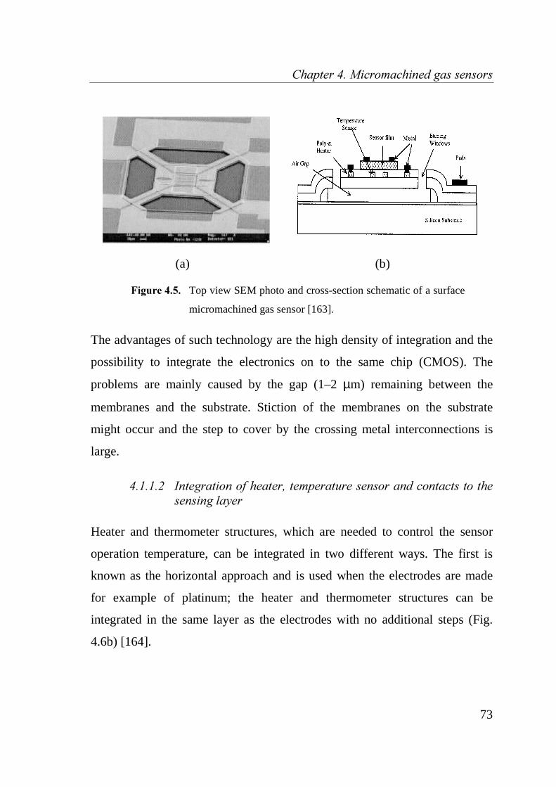
&KDSWHU0LFURPDFKLQHGJDVVHQVRUV
73
(a) (b)
)LJXUH Top view SEM photo and cross-section schematic of a surface
micromachined gas sensor [163].
The advantages of such technology are the high density of integration and the
possibility to integrate the electronics on to the same chip (CMOS). The
problems are mainly caused by the gap (1–2 µm) remaining between the
membranes and the substrate. Stiction of the membranes on the substrate
might occur and the step to cover by the crossing metal interconnections is
large.
,QWHJUDWLRQRIKHDWHUWHPSHUDWXUHVHQVRUDQGFRQWDFWVWRWKH
VHQVLQJOD\HU
Heater and thermometer structures, which are needed to control the sensor
operation temperature, can be integrated in two different ways. The first is
known as the horizontal approach and is used when the electrodes are made
for example of platinum; the heater and thermometer structures can be
integrated in the same layer as the electrodes with no additional steps (Fig.
4.6b) [164].

74
(a) (b)
)LJXUH Schematic cross-section view of (a) vertical or (b) horizontal
approach [21].
However, the design of structures that guarantee both appropriate temperature
(resistance) measurements and homogeneous temperature distributions over
the active area can represent quite a challenge. The second way is the vertical
approach in which the heater and thermometer are made in successive steps as
shown in Figure 4.6a. This approach allows more design flexibility [144].
The heater and thermometer are frequently formed in polysilicon, platinum or
p++ doped silicon, and embedded in silicon oxide or nitride for electrical
isolation [144,147,151,158-160,166-168]. Sometimes these resistive structures
act at the same time as heater and thermometer. Polysilicon can be deposited
by a standard chemical vapour deposition (CVD) process and patterned using
a resist mask and reactive ion etching. Platinum can be evaporated or
sputtered, and patterned by a lift-off process or ion beam etching. Whereas
polysilicon structures can be easily integrated in an IC-process, platinum
elements are generally not [151]. Appropriate thicknesses for polysilicon and
platinum are 0.5 and 0.25 µm, respectively. The sheet resistance of the
polysilicon can be adjusted by n-type doping with POCl3 [169], and it is
possible to fabricate polysilicon with negative temperature coefficient

&KDSWHU0LFURPDFKLQHGJDVVHQVRUV
75
resistance (TCR). This is a large advantage as negative TCR materials
counteract to hot spots whereas heater materials with a positive TCR, such as
platinum, have an amplifying effect on hot spots [146]. On the other hand,
polysilicon heaters suffer from a lack of reliability at high temperature
[170,171]. Another alternative material to form the heater and thermometer is
boron-doped (p++) silicon. The structures are located underneath the
membrane in the silicon substrate and are preserved during the silicon etching
process as p++ etch stop (see Chapter 3) [166,167].
Thermometers have also been realised using aluminium plates with electrical
connections for 4-point temperature measurement [159], or by forward biased
p-n junctions, since the voltage of diodes operated at constant current is
proportional to the absolute temperature [172-173]. The use of aluminium
plates improves the temperature uniformity over the active area (high thermal
conductivity), but limits the sensor operation and annealing temperatures to
values below 500°C.
Electrical connections to the gas-sensitive films are generally made by metal
electrodes, deposited on top of the membranes in the so-called active area. The
electrodes are located underneath the sensing film most of the time, but their
deposition on top of thin gas-sensitive layers has also been realised [174]. The
electrode materials usually employed to contact metal-oxide or polymer
sensitive films are gold and platinum with an adhesion layer underneath (Cr,
Ti, Ta) [22,145,151,162]. In some cases, aluminium and tungsten have also
been used for metal-oxide layers [159,175]. Aluminium is commonly
employed to contact the catalytic metals of MOSFET sensors. Aluminium is
advantageous, as it is the standard metallisation in IC-processes. However, its
contact properties to metal-oxide and polymer sensing films are rather bad,

76
and the maximum operation temperature is limited to about 500°C due to
electromigration.
7KHUPDOGHVLJQ
The thermal characteristics of micromachined gas sensors have to be
optimised mainly with respect to low power consumption and well-controlled
temperature distribution over the sensing area. The physical mechanisms
regulating heat losses have to be understood for optimum thermal design of
the sensing platforms.
Heat transfer occurs due to conduction, convection and radiation. The
different heat transfer pathways of a micromachined platform are illustrated in
Figure 4.7. The heat losses from the heated sensing area are due to heat
conduction through the membrane, and to losses to the surrounding
atmosphere through heat conduction and convection. Radiative losses might
also be taken in account depending on the application.
)LJXUH Heat pathways of a micromachined sensing platform [21].
According to the different pathways of heat transfer, the determination of the
total heat loss and temperature distribution is not an easy task. In the design of

&KDSWHU0LFURPDFKLQHGJDVVHQVRUV
77
a new device, simple models for basic understanding are necessary and, to
minimise the costs of development, extensive simulation studies like FEM
(finite element modelling) simulations are required.
Assuming that the different components of heat flow are additive, the total
heat flow, 4 , can be expressed as:
( )( )
( ) [77*
77*
77*4
DPEKRWUDG
DPEKRWDLUDLU
DPEKRWPPWRW
∆+−×××+
−××+
−××=
44εσ
λ
λ
(4.1)
The first term describes the heat conduction through the closed membrane, the
second the heat conduction through the ambient air, the third heat losses due
to radiation and the last term, ∆[, accounts for unknown heat losses including
free convection. ** , and UDG* are geometric factors, and are empirical
values which contain information about the geometry of the closed or
suspended membrane and its effect on heat losses. KRW7 and 7 denote
respectively the temperature of the hot active area and the ambient
atmosphere. λ and λ are the thermal conductivity of the membrane and the
surrounding atmosphere, respectively, ε the emissivity and σ the Stefan-
Boltzmann constant. In the next sections, the different terms are discussed and
expressions for the geometric factors are obtained.

78
+HDWFRQGXFWLRQWKURXJKWKHPHPEUDQH
For the calculation of heat conduction, one has to deal with a 3-dimensional
problem. Due to the negligible thickness of the membrane compared to its
length, the heat conduction perpendicular to the membrane is generally
neglected.
In the case of a suspended membrane, a further reduction to a one-dimensional
problem is straightforward, as heat conduction occurs basically only along the
suspension beams with length l and sectional area of $ . Conduction within
the membrane plate is negligible in comparison [143] and with 4 beams one
obtains:
( )O
77$4
−×××= λ4 (4.2)
where O$
*
×= 4 (4.3)
For a closed membrane, a simple model is obtained by replacement of the
square membrane by a round one [144] as depicted in Figure 4.8. This leads
to one-dimensional heat conduction problem in cylindrical coordinates which
can be easily solved [31]:
( )( )
!"#$ % !&'%
UU
77G4
/ln
2 −×××= λπ (4.4)
( )()*
UU
G*
/ln
2 ×= π (4.5)
d denotes the thickness of the membrane, and ra and ri the radius of the
membrane and the heated area, respectively. From equations 4.2 and 4.4, it is

&KDSWHU0LFURPDFKLQHGJDVVHQVRUV
79
clear that selection of membrane/suspension beam materials of low thermal
conductivity and thickness is desirable to achieve low thermal losses. In
addition, the length-to-width ratio of the suspension beams and the ratio ra/ri,
should be chosen as large as possible to minimise heat losses.
)LJXUH Replacement of a square membrane by a one-dimensional
circular membrane [21].
In the closed-membrane case, the importance of adequate scaling of the square
heating resistor (edge length a) compared with the square membrane (edge
length b) has been shown by several authors [151,153,169]. The power
consumption as a function of distance between heated area and silicon rim
decreases with increasing distance. Nevertheless for a given distance, the
thermal isolation is practically not improved further [169], the chip silicon rim
remaining close to the ambient temperature. Increasing the membrane size
results only in larger devices, reducing the density of integration
Finally, by computing the heat loss in equation 4.2 and 4.4, it can be clearly
shown that the suspended membrane type provides lower power consumption
than a closed membrane.

80
+HDWORVVHVWRWKHDLU
Heat losses to the surrounding air can occur through two different
mechanisms, i.e. fluid motion and conduction. We can distinguish between
two different types of heat loss by fluid motion: forced convection or
free/natural convection. When there is no fluid motion, heat is transferred only
by conduction.
In the following, forced convection is excluded. Nevertheless, due to the
coupling of the temperature field and thus the fluid field, the calculation of
heat losses to air remains difficult. There are two approaches proposed in the
literature to simplify the calculations.
In the first approach, the fluid motion is neglected [143,169,177]. It is
assumed that there is no significant contribution of convectional fluid motion
because of the small size of the heated structures. The heat transfer to air
occurs only by heat conduction. Under this assumption, it is possible to use a
simple analytical model as an estimate for heat losses to the air as in Ref.
[144]. This model approximates the hot gas sensor and the cold ambient by
concentric spheres with radius ri and ra, respectively. While the model gives a
rough estimate of the heat loss by conduction in air, numerical solutions are
needed to solve the problem correctly. An additional factor affecting
conduction in air, which needs to be considered, is the temperature
dependence of the thermal conductivity of air [178]. To optimise the heat
losses in air using this approach, the heated area has to be minimised and the
distance between the cold die and hot membrane maximised.
Qualitatively, the same can be drawn with the second approach, which takes
fluid motion into account. In this case, empirical heat transfer coefficients are

&KDSWHU0LFURPDFKLQHGJDVVHQVRUV
81
used to describe the heat losses to the air. Heat transfer coefficients are, in
general, empirical values and account for heat transfer due to conduction as
well as fluid motion. The total heat flow, 4 , from a heated membrane area to
the surrounding air can be described as:
( )DPEKRWPDLU 77$4 −××= α (4.6)
with α being the mean heat transfer coefficient. Theoretical determination of
heat transfer coefficients requires knowledge of the temperature field and the
velocity and is rather difficult. However, for certain problems it is possible to
find empirical equations describing heat transfer. Nevertheless, the results
should be considered just as estimates for microhotplates, as the empirical
equations used are actually evaluated for much larger hotplate sizes. On the
other hand, with the help of calculated mean heat transfer coefficients, the
total heat flow above a membrane can be easily calculated. Reduction of
power consumption saving is accomplished by minimising the heated
membrane area and the operation temperature. The latter depends on the
properties of the gas-sensing material.
5DGLDWLRQ
The expression for radiation in equation 4.1 was obtained with the assumption
that the heated membrane area behaves like a grey emitter, i.e. the degree of
emission from the heated membrane is set equal to the degree of absorption
[176]. Under the assumption that the heated membrane area, $, radiates in all
directions, the geometry factor * can be set to ( )$* ×= 2 . Heat losses due
to radiation thus increase with heated membrane area. Generally the heat

82
losses due to radiation amount to only a few percent of the total heat loss
[146,151,153,172]. Nevertheless, due to the T4 –dependency, radiation should
be considered carefully as a potential problem if very high sensor operation
temperatures are applied. Radiative losses can be reduced dramatically by
coating the membrane backside with glossy materials like gold (ε = 0.05)
[179].
.H\SDUDPHWHUVIRUORZSRZHUPLFURPDFKLQHGSODWIRUPV
From the above discussion, some key parameters for minimising the total
power consumption of micromachined gas sensing platforms are:
• thin membranes consisting of materials of low thermal conductivity
should be constructed.
• the heated area should be decreased.
• for closed membranes: heater edge length should be adjusted to the size
of the membrane.
• for suspended membrane, suspension beams with high length-to-width
ratios should be used.
• a large pit depth should be chosen.
• for both types: gold coating at the backside of the membrane.
In this whole discussion, one should not forget that besides low power
consumption, the gas sensor’s functionality and the mechanical stability have
to be maintained.

&KDSWHU0LFURPDFKLQHGJDVVHQVRUV
83
+HDWHUGHVLJQ
The heater design is crucial for control of the temperature distribution over the
active area. The geometries of the heater and the substrate have to be adapted
carefully to achieve a desired temperature distribution. It should be pointed
out that the heating of an active area with constant power per area results in an
inhomogeneous temperature profile. The inner part of the heated area loses
heat to the ambient air and by radiation, whereas the outer part additionally
loses heat by conduction through the membrane. Therefore, the borders of the
active area are colder than the inner part, and spatial variation of heating
power is needed to compensate it. High thermal conductivity films may also
help to improve the uniformity of the temperature distribution.
Two practical approaches have been suggested in the literature to solve this
problem. The first one is to use two heaters: an area heater and a ring heater
[143,172]. The ring heater serves to compensate of the heat losses through the
membrane. One difficulty to this two-heater approach is to determine the
compensating heating power required. The other technique is to use a double-
spiral structure with variable width as the heater [180,181]. A disadvantage
compared to the previous approach is that the temperature homogeneity
depends on the heater design and cannot be adjusted later on.
In general, it is very hard to predict the temperature distribution, and
numerical calculations are needed.
7UDQVLHQWWKHUPDOUHVSRQVH
A simple expression for the thermal transient response of the sensor can be
obtained by assuming the temperature distribution inside the sensor to be

84
uniform, and by using one overall thermal resistance (5th) and capacity (&th) to
describe the thermal behaviour. Heat balance between heating power (P) and
heat losses results in the expression:
5
7W7
GW
WG7&3
−+×= )()( (4.7)
This equation allows the calculation of the temperature response to an
arbitrary heating power input. Solutions can be found using Fourier and
Laplace analysis. For instance, the temperature response to a step function is
given by:
&5H537W7
×=
−××=−−
ττ ,1)( (4.8)
Because the thermal time constant, τ, obtained in this way depends linearly on
thermal resistance and capacity, a sensor with low thermal mass and small
thermal resistance will show faster response. Due to the fact that a small
thermal resistance also leads to an increase in power consumption, there is a
trade-off to make in the choice of the thermal resistance material.
Minimisation with respect to thermal capacity is mainly achieved by a
reduction of the heated mass. This is why suspended membranes show
generally faster thermal response than the larger closed membranes.
7KHUPDOVLPXODWLRQV>@
Numerical approximations of the temperature distribution, the total heat loss
and the transient response can be obtained by replacing the sensor by a set of
points for which temperature is calculated as a function of time. This set of

&KDSWHU0LFURPDFKLQHGJDVVHQVRUV
85
points is called the computational grid or mesh. The right choice of
computational grid is very important to obtain good approximations. An
increase of the number of node points result in better accuracy, but leads at the
same time to an increase of computational time. Therefore, it is often better to
model the parts of the sensor that are subject to large changes in temperature
with a narrow grid and regions with few changes with a rather rough grid.
One way to derive the equations for the node temperatures is to divide the
sensor into elements and apply the heat balance to each individual element.
For each element, a point, e.g. the centre of the element, is selected as a node.
Temperature and thus flow variations over the element are neglected. The
node temperature is considered to be representative of the entire element.
Another possibility is to start with the differential equation, which is the
mathematical description of the heat balance of an infinitesimal element, and
replace the differentials by finite differences expressed in terms of the node-
point temperatures. This method is known as the finite-difference method.
In either case, one has to solve a set of equations relating the temperature at
the nodes to each other. A lot of analysis tools that can take over this work are
available nowadays. Solutions can be found by describing the thermal system
using electrical equivalents and using standard circuit analysis tools such as
SPICE.
An alternative is to use advanced finite-element methods (FEM) such as
ANSYS. FEM describe the solution for a given geometry (one-, two-, or three
dimensional) by means of a finite number of line, surface or volume elements.
These can be chosen arbitrarily. FEM can account for complicated boundary
conditions and temperature-dependent thermal properties. The node equations
can thus become rather complicated. Finite-element methods are therefore

86
available in the form of complete software packages, which include tools for
mesh generation, element definition, equation solving and display of results.
0HFKDQLFDOGHVLJQ
Micromachined gas sensors are not only a challenge with respect to thermal
design but also with respect to mechanical design. With proper design, several
modes of failure can be avoided such as:
• large intrinsic or thermal-induced membrane stress, leading to
deformation (buckling) /breaking of the membrane.
• plastic deformation at the metal-sensing layer contact area.
• deformation / breaking of the membrane due to deposition of the
sensing layer(s).
• bad adherence / peel-off of the sensing layer due to mechanical and
thermal stresses.
• mechanical or thermal induced stress in the metallisation.
• thermometer and heater shift or drift due to mechanical and thermal
stresses.
To avoid these failures, the right sets of process parameters have to be found
and processes need to be well controlled. Thin film mechanical and electrical
properties depend strongly on microstructural characteristics like grain size,
orientation, density, and stoichiometry, and depend on deposition conditions.
Moreover, the microstructures change with number of heat cycles. This can
result in the drift of the electrical and/or mechanical characteristics, but also
presents the possibility to adjust a layer’s properties by annealing steps.

&KDSWHU0LFURPDFKLQHGJDVVHQVRUV
87
Intrinsic stress in single layer or multilayer systems can occur as results of
thermal stress and residual stress [183]. Thermally induced stress is caused by
mismatches in the thermal expansion coefficients of the different films, which
might lead to deformation of the structure, or by non-uniform temperature
distribution, which may in some cases be temperature dependent. The latter
points out that thermal and mechanical design are strongly interdependent.
Residual stresses are due to the fact that the thin films in their deposited form
are not in the most favourable energetic configuration, resulting in
compressive or tensile stress.
Residual stresses are generally much more significant than thermal stress, so
that control of residual stress in single layers and especially multilayer
systems is critical for membrane stability [183]. The resultant residual stress,
σr, of a stacked membrane can be approximated by:
∑∑
=
==++
++=
G
G
GG
GG
1
1
21
2211
...
... σσσσ (4.9)
where Gi and σi are the thickness and intrinsic stress of the different
membrane layers. A low residual tensile stress is favourable for the membrane
of a micromachined gas sensor, since the membrane enters in a compressive
state (hot in the middle, cold on the chip frame) during operation.
To obtain such low residual stress in single layers is difficult. Frequently used
materials such as silicon oxide and silicon nitride show significant
compressive and tensile stress, respectively. However, the right combination
of these materials can lead to acceptable resultant residual stress [168].

88
Moreover, by modifying the stoichiometry, a low-stress silicon nitride film
can be obtained using low-pressure chemical vapour (LPCVD) deposition
[156,157].
The properties of a single layer might change upon annealing and processing
of subsequent layers, thus leading to manifestation of different stress
properties in the layer within the multilayer system than as a single layer.
Therefore, the design and fabrication of a membrane with low intrinsic stress
depends on experimental determination of the residual stress. Methods to
measure residual stress involve curvature measurements of the whole wafer.
In situ stress diagnostic structures like doubly supported beams or Guckel
rings, which rely on warping or buckling, may also be used [183]. Such
experimental check is not only of interest for the design of stable membranes,
but also for achieving the process control required to guarantee reproducible
film structures, and thus mechanical as well thermal properties.
A simple, practical measure for the mechanical stability of micromachined gas
sensors is the production yield [169]. A more realistic view with respect to
mechanical stability under normal sensor operation can be obtained through
use of long-term reliability tests [181,184,185]. The importance of thermal
stress can then also be determined, the membrane stack expand thermally,
leading to additional compressive stress, as mentioned before.
Finally, it should be noted that not only the mechanical properties of thin film
layers, but also the macroscopic dimensions of the membrane itself influence
the stability of the micromachined sensors. Decreasing the lateral dimensions
and increasing the thickness of the membrane and suspension beams can lead
to much greater stability. However, as stability is improved, thermal losses are
generally increased as discussed in 4.1.2. The choice of membrane dimensions

&KDSWHU0LFURPDFKLQHGJDVVHQVRUV
89
is therefore a trade-off between high mechanical strength and small thermal
heat losses.
4.2 CONCLUSION
In this chapter, the main technologies used in the field of micromachined gas
sensors, and the design parameters which influence the thermal and
mechanical properties of such devices, were reviewed. Suitable characteristics
for such devices are low power consumption, high mechanical strength, and
well-controlled temperature distribution across the sensing layer.
The starting point for the production of micromachined gas sensors is the
formation of a thermally isolated heating area on a membrane. Silicon
micromachining is used to release the dielectric membrane on which are
located the active components. In general, there are two different types of
structures for the membrane containing the hotplate: one is the close-
membrane-type, and the other, the suspended-membrane type. In most cases,
the membrane is made of silicon nitride and/or silicon oxide thin films, with
the heater and thermometer embedded in between. Metal electrodes deposited
on top usually form the electrical connections with the gas-sensitive films.
The thermal characteristics of micromachined gas sensors have to be
optimised mainly with respect to low power consumption and well-controlled
temperature distribution over the sensing area. The choice of membrane
dimensions is a trade-off between small thermal heat losses and high-
mechanical strength.


91
RReeffeerreenncceess
[1] D.A. Skoog, F. James Holler, and T.A. Nieman, Principles of instrumental
analysis, 5th Ed., Harcourt Brace College Publishers, USA, 1998, pp. 253-271 and
pp. 673-777.
[2] J.W. Gardner and P.N. Bartlett, Electronic noses: principles and applications,
Oxford University Press, Oxford (UK), 1999.
[3] A. D’Amico, C. Di Natale, and R. Paolese, “Portraits of gasses and liquids by
arrays of nonspecific chemical sensors: trends and perspectives”, Sensors and
Actuators, B 68, pp. 324-330, 2000.
[4] K. Persaud and G. Dodd, “Analysis of discrimination mechanisms in the
mammalian olfactory system using a model nose”, Nature, 299, pp.352-355, 1982.
[5] H.T. Troy Nagle, S.S. Schifman and R. Gutierriez-Osuna, “The How and Why of
Electronic Noses”, IEEE Spectrum, Sept. 1998.
[6] W. Göpel, T.A. Jones, M. Kleitz, I. Lundström, and T. Seiyama (Eds),Chemical
and biochemical Sensors, Part I, VCH, Weinheim, Germany, 1991, 716 pp.
[7] I. Lundström, “Approaches and mechanisms to solid state based sensing”, Sensors
and Actuators, B 35-36, pp. 11-19, 1996.
[8] W. Göpel, “Chemical imaging: I. Concepts and visions for electronic and
bioelectronic noses”, Sensors and Actuators, B 52, pp. 125, 1998.
[9] D.E. Williams, “Semiconducting oxides as gas-sensitive resistors”, Sensors and
Actuators, B 57, pp. 1-16, 1999.
[10] W. Göpel and K.D. Schierbaum, “SnO2 sensors: current status and future
prospects, Sensors and Actuators, B 26-27, pp. 1-12, 1995.
[11] I. Lundström, A. Spetz, F. Winquist, U. Ackelid, and H. Sundgren, “Catalytic
metals and field-effect devices – a useful combination”, Sensors and Actuators, B
1, pp. 15-20, 1990.

92
[12] M. Löfdahl, M. Eriksson, and I. Lundström, “Chemical images”, Sensors and
Actuators, B 70, pp. 77-82, 2000.
[13] K.D. Schierbaum, A. Gerlach, M. Haug, and W. Göpel, “Selective detection of
organic molecules with polymers and supramolecular compounds: applications of
capacitance, quartz microbalance and calorimetric transducers”, Sensors and
Actuators, A 31, pp. 130-137, 1992.
[14] A. D’Amico, C. Di Natale, A. Macagnano, F. Davide, A. Mantini, E. Tarizzo, R.
Paolese, and T. Boschi, “Technologies and tools for mimicking olfaction: status of
the Rome ‘Tor Vergata’ electronic nose”, Biosensors & Bioelectronics, 13, p. 711-
721, 1998.
[15] G. Bidan, “Electroconducting conjugated polymers: new sensitive matrices to buld
up chemical or electrochemical sensors: A review”, Sensors and actuators, B 6, pp.
45-56, 1992.
[16] Z. Deng, D.C. Stone, and M. Thompson, “Selective detection of aroma
components by acoustic wave sensors coated with conducting polymer films”, The
Analyst, 121, pp. 671-679, 1996.
[17] K. Domanský, D.L. Baldwin, J.W. Grate, T.B. Hall, J. Li, M. Josowicz, and J.
Janata, “Development and calibration of field-effect transistor-based sensor array
for measurement of hydrogen and ammonia gas mixtures in humid airAnalytical
Chemistry, 70, pp. 473-481, 1998.
[18] M. Haug, K.D. Schierbaum, G. Gauglitz, and W. Göpel, “Chemical sensors based
upon polysiloxanes: comparaison between optical, quartz microbalance,
calorimetric and capacitive sensors”, Sensors and Actuators, B 11, pp. 383-391,
1993.
[19] T. Eklöv, Methods to improve the selectivity of gas sensors systems, Thesis at
Linköping University, Sweden, 1999, 188 pp.
[20] W. Göpel, “Ultimate limits in the miniaturization of chemical sensors”, Sensors
and Actuators, A 56, pp. 83-102, 1996.

5HIHUHQFHV
93
[21] I. Simon, N. Barsan, M. Bauer, and U. Weimar, “Micromachined metal oxide gas
sensors: Opportunities to improve sensor performance”, Sensors and Actuators, B
73, pp. 1-26, 2001.
[22] V. Demarne and A. Grisel, “An integrated low-power thin-film CO gas sensor on
silicon”, Sensors and Actuators, 13, pp. 301-313, 1988.
[23] I. Lundström, S. Shivaraman, C. Svensson, and L. Lundkvist, “A hydrogen-
sensitive MOS field-effect transistor”, Applied Physics Letters, 26, pp. 55-57,
1975.
[24] M. Johansson, I. Lundström, and L-G. Ekedahl, “Bridging the pressure gap for
palladium metal-insulator-semiconductor hydrogen sensors in oxygen containing
environments”, Journal of Applied Physics, 84, pp. 44-51, 1998.
[25] I. Lundström, “Hydrogen sensitive MOS-structures, Part 1: principles and
applications”, Sensor and Actuators, 1, pp. 403-426, 1981.
[26] J. Fogelberg and L.-G. Petersen, “Kinetic modelling of the H2-O2 reaction on Pd
and of its influence on the hydrogen response of a hydrogen sensitive Pd metal-
oxide-semiconductor device”, Surface Science, 350, pp. 91-102, 1996.
[27] I. Lundström, M. Armgarth, and L-G. Petersson, “Physics with catalytic metal gate
chemical sensors”, CRC Crit. Rev. Solid State Mater. Sci., 15, pp. 201-278,
(1989).
[28] F. Winquist, A. Spetz, M. Armgarth, C. Nylander, and I. Lundström, “Modified
palladium metal-oxide-semiconductor structures with increased ammonia gas
sensitivity”, Applied Physics Letters, 43, pp. 839-841, 1983.
[29] A. Spetz, M. Armgarth, and I. Lundström, “Hydrogen and ammonia response of
metal-silicon dioxide structures with thin platinum gates”, Journal of Applied
Physics, 64, pp. 1274-1283, 1988.
[30] I. Lundström, “Why bother about gas-sensitive field-effect devices”, Sensors and
Actuators, A 56, pp. 75-82, 1996.
[31] S.M. Sze, Semiconductor devices: physics and technology, John Wiley and Sons,
USA, 1985, 523 pp.

94
[32] M. Josowicz and J. Janata, in Chemical sensor technology, Ed. by T. Seiyama,
Elsevier, Amsterdam, 1988, p.153.
[33] M.G.H. Meijerink, M. Koudelka-Hep, N.F. de Rooij, D.J. Strike, J. Hendrikse,
W.Olthuis, and P. Bergveld, “Gas-dependent field effect transistor with an
electrodeposited conducting polymer gate contact”, Electrochemical and Solid-
State Letters, 2 (3), pp. 138-139, 1999.
[34] A. Lloyd Spetz, P. Tobias, A. Baranzahi, P. Martensson, and I. Lundström,
“Current status of silicon carbide based high-temperature gas sensors”, IEEE
Transactions on Electron Devices, 46 (3), pp. 561-566, 1999.
[35] A. Lloyd Spetz, P. Tobias, L. Unéus, H. Svenningstorp, L.-G. Ekedahl, and I.
Lundström, “High temperature catalytic metal field effect transistors for industrial
applications”, Sensor and Actuators, B 70, pp.67-76, 2000.
[36] J.P. Colinge, Silicon-on-insulator technology: materials to VLSI, 2nd Ed., Kluwer
Academic Publishers, The Netherlands, 1997, 272 pp.
[37] D.R. Walt, T. Dockinson, T. White, J. Kauer, S. Johnson, H. Engelhardt, J. Sutter,
and P. Jurs, “Optical sensor arrays for odor recognition”, Biosensors &
Bioelectronics, 13, pp. 697-699.
[38] J. Homola, S.Y. Sinclair, and G. Gauglitz, “Surface plasmon resonance sensors:
review”, Sensors and Actuators, B54, pp. 3-15, 1999.
[39] T. Lang, H.-D. Wiemhöfer, W. Göpel, “Carbonate based CO2 sensors with high
performance”, Sensors and Actuators, B 34, pp. 383-387, 1996.
[40] J.F. Currie, A. Essalik, and J.C. Marusic, “Micromachined thin solid state
electrochemical CO2, NO2, SO2 gas sensors”, Sensors and Actuators, B 59, pp.
235-242, 1999.
[41] A. Accorsi, G. Delapierre, C. Vaucher, and D. Charlot, “A new microsensor for
environmental monitoring”, Sensors and Actuators, B 4,, pp. 539-543, 1991.
[42] M. Zanini, J.H. Visser, L. Rimai, R.E. Soltis, A. Kovalchuk, D.W. Hoffman, E.M.
Logothetis, U. Bonne, L. Brewer, O.W. Bynum, and M.A. Richard, “Fabrication
and properties of Si-based high-sensitivity microcalorimetric gas sensor”, Sensors
and Actuators, A 48, pp. 187-192, 1995.

5HIHUHQFHV
95
[43] J. Lerchner, D. Caspary, and G. Wolf, “Calorimetric detection of volatile
compounds”, Sensors and Actuators, B 70, pp. 57-66, 2000.
[44] Ch. Ziegler, W. Göpel, H. Hämmerle, H. Hatt, G. Jung, L. Laxhuber, H.-L.
Schimdt, S. Schütz, F. Vögtle, and A. Zell, “Bioelectronic noses: a status report.
Part II”, Biosensors & Bioelectronics, 13, pp. 539-571, 1998.
[45] J.W. Gardner and P.N. Bartlett, Pattern recognition in gas sensing, in Techniques
and & mechanisms in gas sensing, Ed. by P.T. Moseley, S.O.W. Norris and D.E.
Williams, The Adam Hilger series on sensors, Bristol (UK), 1991.
[46] D. Gnani, V. Guidi, M. Ferroni, G. Faglia, and G. Sberveglieri, “High-precision
neural pre-processing for signal analysis of a sensor array”, Sensors and Actuators,
B 47, pp. 77-83, 1998.
[47] C. Di Natale, F. Davide, and A. D’Amico, “Pattern recognition in gas sensing:
well-stated techniques and advances”, Sensors and Actuators, B 23, pp. 111-118,
1995.
[48] M. Holmberg, F. Winquist, I. Lundström, J.W. Gardner, and E.L. Hines,
“Identification of paper quality using a hybrid electronic nose”, Sensors and
Actuators, B 26-27, pp. 246-249, 1995.
[49] T.D. Gibson, O. Prosser, J.N. Hulbert, R.W. Marshall, P. Corcoran, P. Lowery,
E.A. Ruck-Keene, and S. Heron, “Detection and simulataneous identification of
microorganisms for headspace samples using an electronic nose”, Sensors and
Actuators, B 44, pp. 413-422, 1997.
[50] K. Esbensen, T. Midtgaard, and S. Schönkopf, Multivariate analysis in practice,
Camo A/S, Trondheim, 1994.
[51] R.G. Brereton, Multivariate pattern recognition in chemometrics, Elsevier,
Amsterdam, 1992.
[52] E. Kress-Rogers, Handbook of biosensors and electronic noses, CRC Press, Inc.,
Boca Raton (USA), 1997.
[53] T. Talou and B. Dubreuil, “E-NOSENET: State of the art on patents in electronic
nose technology”, Conf. Proc. of the of the 6th International Symposium on
Olfaction and Electronic Nose, Tübingen, Germany, Sept. 1999, pp. 38-41.

96
[54] D.J. Strike, M.G.H. Meijerink, and M. Koudelka-Hep, “Electronic noses, a mini
review”, Fresenius Journal of Analytical Chemistry, 364, pp. 499-505, 1999.
[55] E. Zubritsky, “E-noses keep an eye on the future”, Journal of Analytical
Chemistry, 72 (11), pp. 421A-426A, 2000.
[56] H. Baltes, D. Lange, and A. Koll, “The electronic nose in Lilliput”, IEEE
Spectrum, 35, pp. 35-38, 1998.
[57] F. Zee and J.W. Judy, “Micromachined polymer-based chemical gas sensor array”,
Sensors and Actuators, B 72, pp. 120-128, 2001.
[58 ] A. Meckes, J. Behrens, O. Kayser, W. Benecke, Th. Becker, and G. Müller,
“Microfluidic system for the integration and cyclic operation of gas sensors”,
Sensors and Actuators, A 76, pp. 478-483, 1999.
[59] G. Frye-Mason, R. Kottenstette, P. Lewis, E. Heller, R. Manginell, D. Adkins, G.
Dulleck, D. Martinez, D. Sasaki, C. Mowry, C. Matzke, and L. Anderson, “Hand-
held miniature chemical analysis system (µChemLab) for detection of trace
concentrations of gas phase analytes” Micro Total Analysis Systems 2000, Ed. by
A. van den Berg et al., Kluwer Academic Publishers, The Netherlands, 2000.
[60] S.P. Murarka and M.C. Peckerar, Electronic materials: science and technology,
Academic Press, Inc. (USA), 1989, 622 pp.
[61] M. Ohring, The material science of thin films, Academic Press, Inc. (USA), 1992,
704 pp.
[62] M. Madoue, Fundamentals of microfabrication, CRC Press, Boca Raton (USA),
1997, 589 pp.
[63] G.T.A. Kovacs, Micromachined transducers source book, WCB/McGraw-Hill
(USA), 1998, 911 pp.
[64] M. Köhler, Etching in microsystem technology, Wiley-VCH, 1999, 368 pp.
[65] S.A. Campbell and H.J. Lewerenz, Semiconductor micromachining: vol. 1,
Fundamentals of electrochemistry and physics, vol.2 Techniques and industrial
applications, John Wiley & Sons, 1996.
[66] T.W. Harris, Chemical milling, Clarendon Press, Oxford (UK), 1976.

5HIHUHQFHV
97
[67] H.R. Robbins and B. Schwartz, “Chemical etching of silicon –I. The system HF,
HNO3 and H2O” Journal of the Electrochemical Society, 106, pp. 505-508, 1959.
[68] H.R. Robbins and B. Schwartz, “Chemical etching of silicon –II. The system HF,
HNO3, H2O, and HC2C3O2” Journal of the Electrochemical Society, 107, pp. 108-
111, 1960.
[69] B. Schwartz and H.R. Robbins, “Chemical etching of silicon –III. A temperature
study in the acid system”, Journal of the Electrochemical Society, 108, pp. 365-
372, 1961.
[70] B. Schwartz and H.R. Robbins, “Chemical etching of silicon –IV. Etching
technology”, Journal of the Electrochemical Society, 123, pp. 1903-1909, 1976.
[71] J.H. Foster and J.B. Singleton, “Beam-lead sealed junction integrated circuits”
Bell Laboratory Records, 44, pp. 313-317, 1966.
[72] M.P. Lepselter, “Beam lead technology”, Bell Systems Technology Journal, 45,
pp. 233-254, 1966.
[73] T.J. Rodgers, W.R. Hiltpold, D. Frederick, J.J. Barnes, F.B. Jenné, and J.D.
Trotter, “VMOS memory technology”, IEEE Journal on Solid-State Circuits, vol.
SC-12, pp. 515-523, 1977.
[74] T.J. Rodgers, W.R. Hiltpold, J.W. Zimmer, G. Marr, and J.D. Trotter, “VMOS
ROM”, IEEE Journal Solid-State Circuits, vol. SC-11, pp. 614-622, 1976.
[75] E.S. Ammar and T.J. Rodger, “UMOS Transistors on (110) silicon”, IEEE
Transactions on Electron Devices, ED-27, pp. 907-914, 1980.
[76] C.S. Smith, “Piezoresistance effect in germanium and silicon”, Physical Reviews,
94, pp. 42-49, 1954.
[77] W.G. Pfann, “Improvement of semiconducting devices by elastic strain”, Solid-
State Electronics, 3, pp. 261-267, 1961.
[78] O.N. Tuffe, P.W. Chapman, and D. Lomg, “Silicon diffused-element
piezoresistive diaphragms”, Journal of Applied Physics, 33, pp. 3322, 1962.
[79] K.E. Petersen, “Silicon as mechanical material”, Proceedings of the IEEE, 70, pp.
420-457. 1982.
[80] C. Kittel, Introduction to solid state physics, John Wiley & Sons, 1976.

98
[81] M. Alavi, S. Buttgenbach, A. Schumacher, and H.J. Wagner, “Fabrication of
microchannels by laser machining and anisotropic etching of silicon”, Sensor and
Actuators, A 32, pp. 299-302, 1992.
[82] E. Peeters, Process development for 3D silicon microstructures, with application to
mechanical sensors design, Ph.D. Thesis, Catholic University of Louvain,
Belgium, 1994.
[83] D.L. Kendall, “On etching very narrow grooves in silicon”, Applied Physics
Letters, 26, pp. 195-198, 1975.
[84] D.L. Kendall, “Vertical etching of silicon at very high aspect ratios”, Ann. Rev.
Mater. Sci., 9, pp. 373-403, 1979.
[85] A. Uhlir, “Electrolytic shaping of germanium and silicon”, Bell Systems
Technology Journal, 35, pp. 333-347, 1956.
[86] H. Seidel, L. Csepregi, A. Heuberger, and H. Baumgartel, “Anisotropic etching of
crystalline silicon in alkaline solutions- Part I. Orientation dependence and
behavior of passivations layers”, Journal of the Electrochemical Society, 137, pp.
3612-3626, 1990.
[87] H. Seidel, L. Csepregi, A. Heuberger, and H. Baumgartel, “Anisotropic etching of
crystalline silicon in alkaline solutions- Part II. Influence of dopants”, Journal of
the Electrochemical Society, 137, pp. 3626-3632, 1990.
[88] D.B. Lee, “Anistropic etching of silicon”, Journal of Applied Physics, 40, pp.
4569-4574, 1969.
[89] K.E. Bean, R.L. Yeakley, and T.K. Powell, “Orientation dependent etching and
deposition of silicon”, Journal of the Electrochemical Society, 121, pp. 87C, 1974.
[90] P.M. Zavracky, T. Earles, and N.L. Pokrovsky, “Fabrication of vertical sidewalls
by anisotropic etching of silicon (100) wafers”, Journal of the Electrochemical
Society, 141, pp. 3182-3188, 1994.
[91] K. Sato, M. Shikida, T. Yamashiro, M. Tsunekawa, and S. Ito, “Roughening of
single-crystal silicon surface etched by KOH water solution”, Sensors and
Actuators, A 73, pp. 122-130, 1999.

5HIHUHQFHV
99
[92] R.M. Finne and D.L. Klein, “A water-amine-complexing agent system for etching
silicon”, Journal of the Electrochemical Society, 114, pp. 965-970, 1967.
[93] A. Reisman, M. Berkenbilt, S.A. Chan, F.B. Kaufman, and D.C. Green, “The
controlled etching of silicon in catalysed ethylene-diamine-pyrocathechol-water
solution”, Journal of the Electrochemical Society”, 126, pp. 1406-1414, 1979.
[94] M.J. Declercq, L. Gerzberg, and J.D. Meindl, “Optimization of the hydrazine-
water solution for anisotropic etching of silicon in integrated circuit technology”,
Journal of the Electrochemical Society, 122, pp. 545-552, 1975.
[95] M. Mehregany and S.D. Senturia, “Anisotropic etching of silicon in hydrazine”,
Sensors and Actuators, 13, pp. 375-390, 1988.
[96] U. Schanakenberg, W. Benecke, and P. Lange, “TMAHW etchants for silicon
micromachining”, Tech. Digest of the 6th Int. Conf. Solid-State Sensors and
Actuators (Transducers ’91), San-Francisco (CA), USA, 1991, pp. 815-818.
[97] O. Tabata, R. Asahi, H. Funabashi, K. Shimaoka, and S. Sugiyama, “Anisotropic
etching of silicon in T.M.A.H. solutions”, Sensors and Actuators, A 34, pp. 51-57,
1992.
[98] A. Merlos, M. Acero,, M.H. Bao, and J. Esteve, “T.M.A.H./IPA anisotropic
etching characteristics”, Sensors and Actuators, A 37-38, pp. 737-743, 1993.
[99] K. Sato, M. Shikida, T. Yamashiro, K. Asaumi, Y. Iriye, and M. Yamamoto,
“Anisotropic etching rates of single crytal silicon for TMAH water solution as a
function of crystallographic orientation”, Sensors and Actuators, A 73, pp. 131-
137, 1999.
[100] R. Puers, “Mechanical silicon sensors at K.U. Leuven”, Conf. Proc. Thermadag:
SENSOREN, Rotterdam, Netherlands, 1991, pp. 1-8.
[101] C.A. Desmond, C.E. Hunt, and S.N. Farrens, “The effects of process-induced
defects on the chemical selectivity of highly doped boron etch stops in silicon”,
Journal of the Electrochemical Society, 141, pp. 178-184, 1994.
[102] S.D. Collins, “Etch stop techniques for micromachining”, Journal of the
Electrochemical Society, 144, pp. 2242-2262, 1997.

100
[103] B. Kloeck, S.D. Collins, N.F. de Rooij, and R.L. Smith, “Study of electrochemical
etch-stop for high-precision thickness control of silicon membranes”, IEEE
Transactions on Electron Devices, 36, pp. 663-669, 1989.
[104] R. Buser, and N.F. de Rooij, Monolitisches Kraftsensorfeld, VDI Berichte Nr. 667,
Sensoren, Technologien und Anwendung, 1988, pp. 115-118.
[105] B. Puers, and W. Sansen, “Compensation structures for convex corner
micromachining in silicon”, Sensors and Actuaotors, A 21-23, pp. 1036-1041,
1990.
[106] G.K. Mayer, H.L. Offereins, H. Sandmaier, and K. Kühl, “Fabrication of non-
underetched convex corners in anisotropic etching of (100)-silicon in aqueous
KOH with respect to novel micromechanics elements”, Journal of the
Electrochemical Society, 137, pp. 3947-3951, 1990.
[107] P.W. Barth, P.J. Shlichta, and J.B. Angel, “Deep narrow vertical-walled shafts in
<110> silicon” Conf. Proc. 3rd Int. Conf. Solid-State Sensors and Actuators,
Philadelphia (PA), 1985, pp. 371-373.
[108] X. Li, M. Bao, and S. Shen, “Maskless etching of three-dimensional structures in
KOH”, Sensors and Actuators, A 57, pp. 47-52, 1996.
[109] M. Bao, X. Li, S. Shen, and H. Chen, “A novel micromachining technology for
multilevel structures of silicon”, Sensors and Actuators, A 63, pp. 217-221, 1997.
[110] I. Zubel, “Silicon anisotropic etching in alkaline solutions III: On the possibility of
spatial structures forming in the course of Si(100) anisotropic etching in KOH and
KOH + IPA solutions”, Sensors and Actuators, A 84, pp. 116-125, 2000.
[111] J.B. Price, “Anisotropic etching of silicon with KOH-H20- Isopropyl alcohol”,
Semiconductor Silicon 1973, Chicago (IL), USA, 1973, pp. 339-353.
[112] O.J. Glembocki, R.E. Stahlbush, and M. Tomkiewicz, “Bias-dependent etching of
silicon in aqueous KOH”, Journal of the Electrochemical Society, 132, pp. 145-
151, 1985.
[113] M. Elwenspoek, “On the mechanism of anisotropic etching of silicon”, Journal of
the Electrochemical Society, 140, pp. 2075-2080, 1993.

5HIHUHQFHV
101
[114] F. Laermer, A. Schilp, K. Funk, and M. Offenberg, “Bosch deep silicon etching:
Improvements uniformity and etch rate for advanced MEMS applications”, Conf.
Proc. 12th IEEE Int. Conf. On Micro-Electro-Mechanical Systems, Orlando (FL),
(USA), 1999, pp. 211-216.
[115] J. Bhardwaj, H. Ashraf, and A. McQuarrie, “Dry silicon etching for MEMS”,
Conf. Proc. of the 191st Meeting of the Electrochemical Society, Microstructures
and Microfabricated Systems III Symposium”, Montréal (PQ), Canada, 1997, vol
97-5, pp. 118-130.
[116] F. Larmer and A. Schilp, “Method of anisotropically etching silicon”, US-Patent
No. 5501893.
[117] M. Esahi, M. Takinami, Y. Wakabayashi, and K. Minami, “High-rate directional
deep dry etching for bulk silicon micromachining”, Journal of Micromechanics
and Microengineering, 5, pp. 5-10, 1995.
[118] M. Biebl and H. von Philipsborn, Fracture and strength of doped and undoped
panical filters, Ph.D. Thesis, UC Berkeley, 1993.
[119] S. Greek, F. Ericson, S. Johansson, and J.-A. Schweitz, “In-situ tensile strength
measurement of thick-film and thin-film micromachined structures”, Conf. Proc
8th Int. Conf. Solid-State Sensors and Actuators (Transducers 1995), Stockholm,
Sweden, 1995, pp. 56-59.
[120] M. Le Berre, P. Kleimann, D. Semmache, D. Barbier, and P. Pinard, “Electrical
and piezoresian”, McWhorter, Eds., Smart Electronics and MEMS, Proc. of the
Smart Structures and Materials 1996 Meeting, vol. 2722, SPIE, San Diego (CA),
USA, 1996.
[121] C. Linder, L. Paratte, M.-A. Grétillat, V.P. Jaecklin and N.F. de Rooij, “ Surface
micromachining”, Journal of Micromechanics and Microengineering, 2, pp. 122-
132, 1992.
[122] P.J. French, “Development of surface micromachining techniques compatible with
on-chip electronics”, Journal of Micromechanics and Microengineering, 6, pp.
197-211, 1996.

102
[123] J. Bühler, F-P Steiner, and H. Baltes, “Silicon dioxide sacrificial layer etching in
surface micromachining”, Journal of Micromechanics and Microengineering, 7,
R1-R13, 1997.
[124] J.M. Bustillo, R.T. Howe, and R.S. Muller, “Surface micromachining for
Microelectrochemical systems”, Proc. of the IEEE, vol. 86. no. 8. 1998.
[125] H.C. Nathanson, W.E. Newell, R.A. Wickstrom, and J.R. Davis, “The resonant
gate transistor”, IEEE Transactions on Electron Devices, ED-14, pp. 117-133,
1967.
[126] B. Dutta, “Integrated micromotor concepts”. Conf. Proc. of Int. Conf. On
Microelectronics Circuits and Systems Theory, Sydney, Australia, 1970, pp.36-37.
[127] R.T. Howe and R.S. Muller, “Polycrystalline silicon micromechanical beams”
Spring Meeting of the Electrochemical Society, Montréal (PQ), Canada, 1982, pp.
184-185.
[128] H. Guckel and D.W. Burns, “A technology for integrated transducers”, Conf. Proc.
Int. Conf. Solid-State Sensors and Actuators, Philadelphia (PA), USA, 1985, pp.
90-92.
[129] R.T. Howe, “Recent advances in surface micromachining” Tech. Digest 13th
Sensor Symposium, Tokyo, Japan, 1995, pp. 1-8.
[130] K. Gabrial, J. Jarvis, and W. Trimmer, “Small machines, large opportunites: A
report on the Emerging Field of Microdynamics”, National Science Foundation,
1989.
[131] Editor, “Analog devices combines micromachining with BICMOS”,
Semiconductor Internaltional, 14, pp. 17, 1991.
[132] L.J. Hornbeck, “Projection displays and MEMS: Timely convergence for bright
future”, Micro-machining and Microfabrication Process Technology, (Proceedings
of SPIE), Austin (TX), USA, 1995, pp. 2.
[133] R.T. Howe and R.S. Muller, “Polycrystalline silicon mechanical beams”, Journal
of the Electrochemical Society, 130, pp. 1420-1423, 1983.

5HIHUHQFHV
103
[134] R.T. Howe, Polycrystalline silicon structures, in Micromachining and
Micropackaging of Transducers, Eds. by C.D Fung, P.W. Cheung, W.H. Ko, and
D.G. Fleming, Elsevier, NY, USA, 1985, pp. 169-187.
[135] W. Yun, A surface micromachined accelerometer with integrated CMOS detection
circuitry, Ph.D. Thesis, U.C. Berkeley, 1992.
[136] A.C. Adams, Dielectric and polysilicon film deposition, in VLSI Technology, Ed.
by S.M. Sze, McGraw-Hill, 1988, pp. 233-271.
[137] N. Taguchi, Japanese Patent 45-38200.
[138] N. Taguchi, Japanese Patent 47-38840.
[139] N. Taguchi, US Patent 3 644 795.
[140] Figaro Products Catalogue, Figaro gas sensors 2000-series, Figaro Engineering
Inc., European Office, Oststrasse 10, 40211 Düsseldorf, Germany.
[141] FIS, Product list (Specifications: Sb/sp series), FIS Inc. (May 1999).
[142] UST, Product Information (1999), Umweltsensortechnik GmbH, Gewerbegebiet
Geschwenda Süd 3, 98716, Geschwenda, Germany.
[143] S. Fung, Z. Tang, P. Chan, J. Sin, and P. Cheung, “Thermal analysis and design of
a micro-hotplate for integrated gas-sensor applications”, Sensors and Actuators, A
54, pp. 482-487, 1996.
[144] G. Sberveglieri, W. Hellmich, and G. Müller, “Silicon hotplates for metal oxide
gas sensors elements”, Microsystem Technologies, 3, pp. 183-190, 1997.
[145] J. Gardner, A. Pike, N.F. de Rooij, M. Koudelka-Hep, P.-A. Clerc, A. Hierlemann,
and W. Göpel, “Integrated array sensor for detecting organic solvents”, Sensors
and Actuators, B 26-27, pp. 135-139, 1995.
[146] A. Götz, I. Gràcia, C. Cané, E. Lora-Tamayo, M. Horillo, G. Getino, C. Gràcia,
and J. Gutiérrez, “A micromachined solid state integrated gas sensor for detection
of aromatic hydrocarbons”, Sensors and Actuators, B 44, pp. 483-487, 1997.
[147] D. Briand, O. Guenat, B. van der Schoot, T. Hirata, and N.F. de Rooij, “Micro-
hotplate, a useful concept for gas-sensing, fluidics and space applications”, Conf.
Proc. of Microfabricated Systems and MEMS V, 198th ECS Meeting, 2000, pp.
151-158.

104
[148] R.J. Reay, E.H. Klaassen, and G.T.A. Kovacs, “Thermally and electrically isolated
single crystal silicon structures in CMOS technology”, IEEE Electron Device
Letters, 15, pp. 399-401, 1994.
[149] C. Rossi, D. Estève, and C. Mingues, “Pyrotechnic actuator: a new generation of
Si integrated actuator”, Sensors and Actuators, A 74, pp. 211-215, 1999.
[150] A.P. Lee and B.J. Reedy, “Temperature modulation in semiconductor gas
sensing”, Sensors and Actuators, B 60, pp. 35-42, 1999.
[151] D.-D. Lee, W.-Y. Chung, M.-S. Choi, and J.M. Baek, “Low-power micro gas
sensor”, Sensors and Actuators, B 33, pp. 147-150, 1996.
[152] P. Maccagnani, R. Angelucci, P. Pozzi, L. Dori, A. Parisini, M. Bianconi, and G.
Benedetto, “Thick porous silicon thermo-insulating membranes”, Sensors and
Materials, 11, pp. 131-147, 1999.
[153] S. Astié, A. Gué, E. Schied, L. Lescouzères, and A. Cassagnes, “Optimization of
an integrated SnO2 gas sensor using a FEM simulator”, Sensors and Actuators, A
69, pp. 205-211, 1998.
[154] M. Dumitrescu, C. Cobianu, D. Lungu, D. Dascalu, A. Pascu, S. Kolev, and A.
van den Berg, “Thermal simulation of surface micromachined polysilicon
hotplates of low power consumption”, Sensors and Actuators, A 76, pp. 51-56,
1999.
[155] M. von Arx, O. Paul, and H. Baltes, “Process-dependent thin-film thermal
conductivities for thermal CMOS MEMS”, Journal of Microelectromechanical
Systems, 9, pp. 136-145, 2000.
[156] M. Sekimoto, H. Yoshhara, and T. Ohkubo, “Silicon nitride single-layer x-ray
mask”, Journal of Vacuum Science Technology, 21, pp.1017-1021, 1982.
[157] C.H. Mastrangelo, Y.-C. Tai, and R.S. Muller, “Thermophysical properties of low-
residual stress, silicon-rich, LPCVD silicon nitride films”, Sensors and Actuators,
A 21-23, pp. 856-860, 1990.
[158] S. Wessel, M. Parameswaran, S.R. Morrison, and R.F. Frindt, “A CMOS
thermally isolated heater structure as a substrate for semiconductor gas sensors”,
Microelectronics Journal, 23, pp. 451-456, 1992.

5HIHUHQFHV
105
[159] J.S. Suehle, R.E. Cavicchi, M. Gaitan, and S. Semancik, “Tin oxide gas sensor
fabricated using CMOS micro-hotplates and in-situ porcessing”, IEEE Electron
Device Letters, 14, pp. 118-120, 1993.
[160] L. Sheng, Z. Tang, J. Wu, P.C.H: Chan, and J.K.O. Sin, “A low-power CMOS
compatible integrated gas sensor using maskless tin oxide sputtering”, Sensors and
Actuators, B 49, pp. 81-87, 1998.
[161] C. Düsco, E. Vàzsonyi, M .Adám, I. Szabó, I. Bársony, J. Gardeniers, and A. van
den Berg, “Porous silicon bulk micromachining for thermally isolated membrane
formation”, Sensors and Actuators, A 60, pp. 235-239, 1997.
[162] F. Solzbacher, C. Imawan, H. Steffes, E. Obermeier, and H. Möller, “A modular
system of SiC-based microhotplates for the application in metal oxide gas
sensors”, Sensors and Actuators, B 64, pp. 95-101, 2000.
[163] P. Mardilovich, D. Routkevitch, and A. Govyadinov, “Hybrid micromachining and
surface microstructuring of alumina surface”, Conf. Proc. of Microfabricated
Systems and MEMS V, 198th ECS Meeting, 2000, pp. 33-42.
[164] P.C.H. Chan, G.-z. Yan, L.-y- Sheng, R.K. Sharma, Z. Tang, J.K.P. Sin, I.-M.
Hsing, and Y. Wang, “An integrated gas sensor technology using surface
micromachining”, Conf. Proc. of 14th IEEE Int. Conf. on Micro-Electro-
Mechanical Systems (MEMS’01), Interlaken, Switzerland, 2001, pp. 543-546.
[165] W.-Y. Chung, J.-W. Lim, D.-D- Lee, N. Miura, and N. Yamazoe, “Thermal and
gas-sensing properties of planar-type micro gas sensor”, Sensors and Actuators, B
64, pp. 118-123, 2000.
[166] S. Majoo, J.L. Gland, K.D. Wise, and J.W. Schwank, “A silicon micromachined
conductometric gas sensor with a maskless Pt sensing film deposited by selected-
area CVD”, Sensors and Actuators, B 35-36, pp. 312-319, 1996.
[167] Z. Tang, S.K.H. Fung, D.T.W. Wong, P.C.H. Chan, J.K.O. Sin, P.W. Cheung, “An
integrated gas sensor based tin oxide thin-film and improved micro-hotplate”,
Sensors and Actuators, B 46, pp. 174-179, 1998.

106
[168] C. Rossi, P. Temple-Boyer, and D. Estève, “Realization and performance of thin
SiO2/SiNx membrane for microheater applications”, Sensors and Actuators, A 64,
pp. 241-245, 1998.
[169] A. Götz, I. Gràcia, C. Cané, and E. Lora-Tamayo, “Thermal and mechanical
aspects for designing micromachined low-power gas sensors”, Journal of
Micromechanics and Microengineering, 7, pp. 247-249, 1997.
[170] N.R. Swart and A. Nathan, “Reliability study of polysilicon microhotplates”, Conf.
Proc. Solid-State Sensor and Actuator Workshop, Hilton Head, South Carolina,
USA, 1994, pp. 119-122.
[171] O. Grudin, R. Marinescu, L. Landsberger, D. Cheeke, and M. Kahrizi,
“Microstructure release and test techniques for high temperature micro hotplate”,
Conf. Proc. of the IEEE Canadian Conference on Electrical an Computer
Engineering, Edmonton (Alberta), Canada, 1999, pp. 1610-1615.
[172] P. Hille and H. Stack, “A heated membrane for a capacitive gas sensor”, Sensors
and Actuators, A 32, pp. 321-325, 1992.
[173] C. Saul and J. Zemel, “Diode-based microfabricated hot-plate sensor”, Sensors and
Actuators, A 65, pp. 128-135, 1998.
[174] M. Hausner, J. Zacheja, and J. Binder, “Multi-electrode substrate for selectivity
enhancement in air monitoring”, Sensors and Actuators, B 43, pp. 11-17, 1997.
[175] S. Semancik and R.E. Cavicchi, “Kinetically controlled chemical sensing using
micromachined structures”, Accounts of Chemical Research, 31, pp. 279-287,
1997.
[176] H. Baehr and K. Stephan, Wärme- und Stoffübertragung, 3rd Edition, Springer,
1998.
[177] A. Van Herwaarden and G. Meijer, Thermal sensors, in S.M. Sze (Ed.)
Semiconductor Sensors, John Wiley & Sons Inc, 1994, pp. 331-382.
[178] U. Grigull and H. Sandner, Wärmerleitung, Springer Verlag, 1979.
[179] S. Möller, J. Lin, and E. Obermeier, “Material and design considerations for low-
power microheater modules for gas-sensor applications”, Sensors and Actuators, B
24-25, pp. 343-346, 1995.

5HIHUHQFHV
107
[180] R. Aigner, M. Dietl, R. Katterloher, and V. Klee, “Si-planar-pellistor: design for
temperature modulated operation”, Sensors and Actuators, B 33, pp. 151-155,
1996.
[181] V. Guidi, G. Cardinali, L. Dori, G. Faglia, M. Ferroni, G. Martinelli, P. Nelli, and
G. Sberveglieri, “ Thin-film gas sensor implemented on a low-power consumption
micromachined silicon structure”, Sensors and Actuators, B 49, pp. 88-92, 1998.
[182] G. Meijer and A. van Herwaarden, Thermal Sensors, Sensors Series, Institute of
Physics, Publishing Bristol and Philadelphia, 1994.
[183] C. Mastrangelo and W. Tang, Semiconductor sensor technologies, in S.M. Sze
(Ed.) Semiconductor Sensors. John Wiley & Sons Inc, 1994, pp. 17-95.
[184] H. Low, M. Tse, and M. Chiu, “Thermal induced stress on the membrane in
intergrated gas sensor with micro-heater”, Conf. Proc. 1998 IEEE Honk-Kong
Electron Devices Meeting, 1990, pp. 140-143.
[185] J. Bosc, Y. Guo, V. Sarihan, and T. Lee, “Accelerated life testing for micro-
machined chemical sensors”, IEEE Transactions on Reliability, 47, pp. 135-141,
1998.


109
SSuummmmaarryy ooff ppaappeerrss
In this work, the power consumption of metal-oxide and MOSFET gas sensors
was lowered using a combination of thin film and micromachining processes.
Devices with improved thermal and gas sensing properties were designed,
fabricated and simulated. The published articles and manuscripts that have
emerged from the results of the experimental work are compiled in the
upcoming papers. The following paragraphs summarise the topics covered by
the papers, as well as their contributions to the field.
Paper I. Design and fabrication of high temperature micro-hotplates for drop-coated gas sensors
The first paper deals with the design and fabrication of micro-hotplates for
drop-coated metal-oxide gas sensors for high temperature operation. Different
dimensions, geometries and materials were investigated with the aim of
lowering power consumption, improving temperature distribution and
withstanding operation at high temperature. Micro-hotplates which could
withstand annealing temperatures and temperature-pulsed modes of operation
up to 700°C were demonstrated. Regarding the fabrication, deep reactive ion
etching of silicon was used to increase the integration density, and a silicon
island was added underneath the membrane to obtain a homogeneous
temperature distribution over the sensing area.

110
Paper II. Thermally isolated MOSFET for gas sensing application
The concept of a micro-hotplate having a silicon island presented in the
previous paper was used to thermally isolate MOSFETs for gas sensing
applications. An implanted resistor and a diode, used respectively as heater
and temperature sensor, and 4 MOSFETs were integrated on a micro-hotplate.
The thermal efficiency of the device was 2°C/mW, with a thermal constant
less than 100 ms. This low-thermal mass device allowed the operation of the
sensors in a pulsed or cycled temperature mode, and the monitoring of the
field and thermal effects in the presence of sample gases.
Paper III. A low-power micromachined MOSFET gas sensor
This paper is an extension of the communication presented in paper II. More
details are given about how the combination of microelectronics and MEMS
(silicon micromachining) processing technologies was used to fabricate the
sensor.
Paper IV. New modes of operation for MOSFET gas sensors using low-power devices
The pulsed and modulated modes of operation for MOSFET gas sensors were
investigated using the low-power, micromachined MOSFET device. Cycling
the temperature during gas exposure modified the kinetics of the gas reactions
with the sensing film. The way in which sensor response was modified

6XPPDU\RISDSHUV
111
depended on the nature of the analyte gas and the catalytic sensing film.
Pulsing the temperature higher after gas exposure was found to reduce the
recovery time in specific applications. It was also possible to discriminate
between gases in a gas mixture by using a sinusoidal-type of temperature
modulation. Perspectives on new modes of operation are also presented.
Silicon-on-insulator (SOI) technology is introduced as a good candidate to
both reduce the power consumption of MOSFET sensors and to increase their
operating temperature.
Paper V. Thermal optimisation of micro-hotplates having a silicon island
Thermal measurements and finite-element-modelling (FEM) were performed
with the aim of optimising the power consumption and temperature
distribution of micro-hotplates for metal-oxide and MOSFET gas sensors. The
work concentrated mainly on micro-hotplates having a silicon island
underneath the sensing area. The thickness of the silicon island was optimised
to lower the power consumption of the devices and still maintain a
homogeneous temperature distribution over the sensing area. The thermal
conductivity of the silicon and the dielectric membrane, the operating
temperature, the geometry and area of the heater, and the processing of the
silicon island were considered in the optimisation process.


113
33DDSSHHUU,,


3XEOLVKHGLQ6HQVRUVDQG$FWXDWRUV%SS 115
DDEESSIIGGNN AANNDD FFAABBRRIICCAATTIIOONN OOFF HHIIGGHH TTEEMMPPEERRAATTUURREE
MMIICCRROO--HHOOTTPPLLAATTEESS FFOORR DDRROOPP--CCOOAATTEEDD GGAASS SSEENNSSOORRSS
Danick Briand1, Andreas Krauss2, Bart van der Schoot1, Udo Weimar2,
Nicolae Barsan2, Wolfgang Göpel2, and Nicolaas F. de Rooij1
1Institute of Microtechnology, University of Neuchâtel, Rue Jaquet-Droz 1,
P.O. Box 3, CH-2007 Neuchâtel, Switzerland 2Institute of Physical Chemistry, University of Tübingen,
Auf der Morgenstelle 6, 72076 Tübingen, Germany
ABSTRACT
This paper reports on the optimisation of micromachined hotplates for gas-
sensing applications designed to withstand high temperature coating processes
and modes of operation. Different thin film materials, geometry and
dimensions have been investigated regarding to their power consumption,
their temperature distribution over the sensing area and their robustness when
annealed at high temperature. In comparison with oxide films, the micro-
hotplates made of nitride were the most robust. They withstood annealing
temperatures up to 700°C and a pulsed temperature mode of operation. Their
robustness allowed the sensing area be heated up to a high temperature (550-
700°C). These micro-hotplates are therefore suitable for the annealing “on-
chip” of the gas-sensitive materials deposited in a drop coating procedure.
Sensors coated with a Pd-doped tin oxide drop and annealed using the

PAPER I
116
integrated heater have been tested under different concentrations of CO and
CH4 in air.
1.1 INTRODUCTION
Micro-hotplates have a tremendous importance in the field of high-
temperature gas-sensing devices (e.g. metal oxide) since they allow the
reduction of the sensor power consumption and the use of new modes of
operation such as temperature cycling due to their low thermal mass [1-6].
SnO2-based nanocrystalline thick film deposited on micromachined hotplates
have been investigated during the past years at the Institute of Physical
Chemistry (IPC), University of Tübingen, Tübingen, Germany as a
combination of thick film and thin film technology for gas detection [6,7].
Thick film technology is well established in the field of the gas-sensitive
materials. Moreover the use of micro-hotplates as substrate makes this
technology suitable for markets where low-power consumption, low-cost and
reliable devices are needed, such as in the portable instruments and in the
automotive industry.
The micro-hotplates previously fabricated at the Institute of Microtechnology
(IMT), University of Neuchâtel, Neuchâtel, Switzerland, could be annealed at
temperatures not higher than 550°C and were unsuitable for long-term
operation in a pulsed temperature mode [7,8]. The adhesion of the coating and
the stability of the sensors were limited by the lack of robustness of the
devices at very high temperature. In this communication, we report on the
design, fabrication and characterisation of micro-hotplates, used in a drop-

'HVLJQDQGIDEULFDWLRQRIKLJKWHPSHUDWXUHPLFURKRWSODWHV«
117
coating procedure of the gas sensitive materials, with the aim of improving
their performance at high temperatures.
The design has been supported using thermal finite element modeling (FEM)
simulations (MEMCAD software from Microcosm Technologies Inc.) [9].
The micro-hotplates are made using backside bulk micromachining of silicon.
The annealing of chemically vapor deposited (CVD) oxide films (to obtain a
low-stress film), the adding of a localised silicon island underneath the
membrane and the use of deep reactive ion etching (DRIE) to release the
membrane have been investigated. Micro-hotplates having an improved
temperature distribution over the sensing area and a higher density of
integration are presented. The optimised devices withstand high annealing
temperatures (700°C) and a pulsed temperature mode of operation.
Moreover, they allow the annealing “on chip” of the coating material, which
was not possible before. The annealing “on chip” of the coating is very
interesting for device packaging, as it will be discussed in the following pages.
The first results concerning the gas sensitivities (CO, CH4, %RH) of a Pd-
doped tin oxide film annealed “on chip” are also reported.
1.2 DESIGN
3RZHUFRQVXPSWLRQDQGUREXVWQHVV
In the aim of reducing the gas sensors power consumption, the micro-hotplates
were made using backside silicon micromachining in KOH to release a thin
dielectric membrane (Fig. 1.1). The membrane thermally isolated the heated
sensing area from the silicon chip frame.

PAPER I
118
/3&9'6LQLWULGH
PHPEUDQH
6L
P
RUPP
3W+HDWHU
(OHFWURGHV
2SWLRQDO
/3&9'6LQLWULGH/3&9'6LQLWULGH
RU&9'6L2
(a)
/3&9'6LQLWULGH
PHPEUDQHP
6L
P
RUPP
+HDWHU
(OHFWURGHV
2SWLRQDOSDVVLYDWLRQ
/3&9'6LQLWULGH/3&9'6LQLWULGH
LQVXODWRUP
6LLVODQG
RUP
(b)
)LJXUH Micro-hotplates schematic without (a) and with (b) Si-island.
The micro-hotplates were made up of a heater stacked between a membrane
and an insulator, on which the interdigited electrodes (IDE 5-50 µm) were
laid. The membrane sizes investigated were 1.0 1.0 and 1.5 1.5 mm2.
The heater and electrode areas were respectively 500 500 µm2 and 750
750 µm2. These dimensions have been chosen with regard to the results of
previous works reported in the literature concerning the decrease of micro-
hotplate power consumption [2,10-12] and were limited by the minimum
droplets size (400 400 µm2) used in the coating procedure of the gas-
sensitive material.

'HVLJQDQGIDEULFDWLRQRIKLJKWHPSHUDWXUHPLFURKRWSODWHV«
119
Different thin film materials of varying thickness have been investigated to
improve robustness (Fig. 1.1). The membrane was made up of a low-stress
LPCVD silicon nitride with a film thickness between 0.25 and 0.5 µm.
Platinum (250 nm) with an adhesive layer of tantalum (20 nm) was used for
the heater (≅ 150-190 Ω at RT, TCR = 0.0020/°C) and the electrodes (150
nm). The insulation layer consisted of a low-stress LPCVD silicon nitride or
an annealed CVD oxide film (0.5 µm). Annealing of the CVD oxide films was
performed to stabilise their microstructures at a high temperature with a
residual tensile stress. The passivation layer consisted of a low-stress LPCVD
nitride (0.2 µm). PECVD silicon nitride thin films were avoided. From our
previous experiences, they were not suitable for annealing and operating at a
temperature higher than 500-550°C [7].
7HPSHUDWXUHGLVWULEXWLRQ
The temperature distribution was optimised by studying different heater
geometry such as simple and double meander. On a series of devices, a ≅ 10-
µm-thick silicon island was added underneath the membrane (Fig. 1.1b) to
improve the homogeneity of the temperature distribution on the sensing area,
which was confirmed by using FEM simulation [9].
'HQVLW\RILQWHJUDWLRQ
Holes having vertical walls can be etched by DRIE of silicon. Using this
technology to release the membranes, the densities of the devices fabricated
were increased compared to using wet anisotropic etching of silicon. DRIE
also gives more flexibility in the design of the device in such a way that the

PAPER I
120
crystal planes of the silicon wafer do not restrict the geometry of the
membrane. Moreover, no protection of the wafer frontside was needed during
the silicon etching if the gas-sensitive material was deposited prior to the
silicon micromachining.
1.3 TECHNOLOGY
0LFURKRWSODWHVIDEULFDWLRQ
The standard fabrication process was as follows. The starting material was a
(100) double-sided polished silicon wafer with a thickness of 400 µm. A
thermal oxide of 50 nm was grown in the case where the hotplates were made
by wet chemical etching of silicon. The 0.25–0.5-µm-thick membrane film
(LPCVD nitride) was then deposited and followed by the lift-off of platinum
(0.25 µm) to make the heater. The heater was covered up with a 0.5-µm-thick
insulation layer (LPCVD nitride or annealed CVD oxide). After the opening
of the contact areas, the Pt electrodes (0.15 µm) were patterned by lift-off and
the devices were covered by an LPCVD nitride passivation film (0.15 µm).
The latter protects both sides of the wafer during the silicon etching in KOH
(40%, 60°C). Once the membrane was released in KOH, the wafer was dipped
in BHF to totally remove the oxide underneath the membrane. Then, the
passivation film was completely or partially (on the sensing area and the pads)
removed by RIE depending on the application. Finally, the wafers were
covered with resist and then diced. The dicing procedure did not affect either
the fabrication yield or the performance of the devices.

'HVLJQDQGIDEULFDWLRQRIKLJKWHPSHUDWXUHPLFURKRWSODWHV«
121
The silicon oxide film used as insulation between the heater and the electrodes
were deposited at 400°C by APCVD. After deposition, the films were
densified (15 min : 625°C/N2) and showed a remaining stress of about 215
MPa (TENCOR instrument). Subsequent annealing of the CVD oxide films at
625° (up to 1 h) and at 800°C (15 min–1 h) were performed to stabilise them
before the following processes done at higher temperatures: the LPCVD at
800°C and the drop coating at 700°C. The annealing temperatures chosen
were compatible with the standard fabrication processes used at IMT. In this
way, it was possible to vary the stress in the layer between 250 MPa to 5 MPA
(625°C : 1h; 800°C : 1h). CVD oxide films with three different stresses of
about 5, 75 and 165 MPa were used as insulator in the micro-hotplates
fabrication (see results in Table 1.1.).
7DEOH Stress in annealed CVD oxide films.
CVD silicon dioxide anneals (530 nm) Stress beforeannealing
Stress afterannealing
Anneal a : 625°C 15 min 250 MPa 213 MPaAnneal b : 625°C 1 h 250 MPa 167 MPaAnneal c : 625°C 1 h + 800°C 15 min 250 MPa 76 MPaAnneal d : 625°C 1 h + 800°C 1 h 250 MPa 7 MPaAnneal e : 625°C 1 h + 800°C 4 h 250 MPa -85 MPa
Variations in the processing were either the DRIE of silicon or the fabrication
of a silicon island underneath the membrane using two etching steps in KOH.
With respect to the DRIE of silicon, the passivation nitride film was not
necessarily on the wafer frontside. A photoresist film (AZ-4562) was used to

PAPER I
122
protect the wafer backside during the silicon etching. The thermal oxide, 300
nm thick for this process, acts as the membranes’ etch stop.
In the case where there is a silicon island remaining under the membrane, the
island is made with two successive KOH etching steps using different
masking, instead of a heavy boron implantation (etch stop) as presented in
Ref. [13]. The process is similar to the one used at IMT to thermally isolate
GasFETs (Gas-sensitive FETs) from the silicon chip frame [14] and is
presented in Figure 1.2.
Firstly, 10 µm of silicon was etched in KOH (40%, 60°C) to define the silicon
island that was protected by the thermal oxide film. The LPCVD Si-nitride
film served to protectt the surrounding silicon (Fig. 1.2a). Secondly, after
removing the oxide mask in BHF, the silicon was etched in 52% KOH (60°C)
all over the window opened in the silicon nitride (Fig. 1.2b). The silicon island
formed during the first etching step is then vertically and horizontally etched
respectively along the <100> and <311> cristallographic axes, respectively
[15]. Therefore, a concentration of 52% of KOH was used to perform the
second silicon etching to decrease the (311) planes’ etch rate to obtain the
desired island width (covering the sensing area). Since the lateral planes (311)
forming the silicon island sides have a higher etch rate than the planes
appearing at the corners (410), no compensation structures were needed [15]
(Fig. 1.2a). The process ended when the membrane was reached. Time was
critical since there was no etch stop to preserve the silicon island thickness.

'HVLJQDQGIDEULFDWLRQRIKLJKWHPSHUDWXUHPLFURKRWSODWHV«
123
Si-plug
850 µm
(111)
(100)
(311)10 µm
Si (100)
(111) oxidenitride
)LJXUH Fabrication process of the silicon island using wet anisotropic
etching of silicon with two masks: (a) with an oxide mask to
define the 10 µm thick silicon island in 40% KOH, (b) with the
oxide remove to release the membrane in 52% KOH.
'URSFRDWHGJDVVHQVRUIDEULFDWLRQ
The annealing of the drop gas-sensitive coating can be performed in a belt
oven or “on chip” using the integrated heater. In the case where a belt oven
was used, the hotplates were first cleaned (acetone/isopropanol) and then
coated. A reproducible drop of coating material with a diameter between 400
and 700 µm depending on the film preparation and the hotplate diameter was
added using a drop-coating method. More information about the preparation
of the sensitive material can be found in Refs [16,17]. The chip was then
annealed up to 700°C (10–20 min). The typical resistance of the coated device

PAPER I
124
was between 1 kΩ to 10 MΩ. Differences in value depend on the doping (e.g.
Pt, Pd, undoped) and on the electrodes gaps.
The chips were mounted in a TO-5 package. The devices were glued using the
conductive glue (No. CW2200MTP from Chemtronics, USA). All the contacts
of the device (two sensor and two heater contacts) are connected to the four-
pin TO-5 socket using a glue drop for each connection. The glue fixes the dice
mechanically and provides the electrical connections. Figure 1.3 shows a
micro-hotplate mounted in a packaging and coated with tin oxide.
TO-5 Socket (4-pin)
Conductive Glue
Tindioxide Paste
)LJXUH Schematic cross-section view of a packaged sensor.
In the case of the annealing “on chip” of the drop-coated films, the micro-
hotplates were packaged before the annealing. The packaging and the coating
were performed using the procedures explained before. Micro-hotplates
having a 1.5 1.5-mm2 membrane (0.5 µm) and an insulation (0.5 µm) film
made up of low-stress LPCVD were used due to their high robustness. Four
sensors (S1, S2, S3, S4) with interdigited electrodes (50 µm) were coated with
a spot of 2% Pd-doped nanocrystalline tin dioxide material (diameter of about
400 µm). The annealing “on chip” was performed with a heater (190 Ω)
voltage of 6 (S0), 7 (S1, S2) and 8 V (S3, S4). The annealing time was 10 s for

'HVLJQDQGIDEULFDWLRQRIKLJKWHPSHUDWXUHPLFURKRWSODWHV«
125
S1 and S3 and 10 min for S0, S2 and S4. The shortest time was selected to test
another annealing condition, which would be compatible with a later
manufacturing process, and the other to have one sensor processed similar to a
belt oven-annealing procedure. The power consumption during the annealing
at 7 V and 8 V were about 115 mW and 160 mW and corresponded to a
temperature of about 500°C and 600°C, respectively.
1.4 CHARACTERISATION AND RESULTS
0LFURKRWSODWHV UREXVWQHVV SRZHU FRQVXPSWLRQ DQG WHPSHUDWXUH
GLVWULEXWLRQ
The micro-hotplates mechanical properties were characterised, from the yield
and robustness to the pulsed temperature operation and high annealing
temperatures. The fabrication yield is considered as the percentage of micro-
hotplates with their membranes not broken during the fabrication process. The
Si-nitride micro-hotplates have higher fabrication yield (98–100%).
Concerning the micro-hotplates with a CVD oxide film as insulation layer, the
passivation layer has to be partially removed on the sensing area after the
etching in KOH to increase their yield and their robustness. Annealing of the
oxide film at 625°C: 1h or 600°C: 1h + 800°C: 15 min (stress of ≅ 165 MPa
and 75 MPa) provides the highest fabrication yield (90–95%) and mechanical
robustness. CVD oxide films annealed successively at 625°C: 1h and 800°C:
1h with no nitride passivation film remaining gave the lowest results with a
yield of about 40%.

PAPER I
126
Switching (100 cycles) of the heater voltage (0–9.5 V / ≅700°C) has shown
that nitride micro-hotplates are very robust (none broke of the 16 tested).
Nitride / oxide micro-hotplates are less robust (at 9.5 V, three broke of the 14
tested). Both designs were also able to stand the annealing process used in a
drop-coating process of the gas-sensitive element: 350°C: 4 min; 550°C: 8
min; 700°C: 10–20 min; 550°C: 8 min; and 350°C: 4 min in a belt oven.
Micro-hotplates with silicon island are more brittle and, in operation, their
breakdown occurred at about 500–550°C.
The evaluation of the thermal properties, such as the power and the
temperature distribution, were made using the integrated heater and an
infrared camera AVIO 2100, with a pixel resolution of 12.5 20 µm2.
Thermal observations were recorded at ambient pressure and at room
temperature. The resistance dependence on the voltage 5(9) and the maximum
temperature 5(7 ) under these conditions were monitored. Figure 1.4
presents the variation of the temperature as a function of power consumption
for nitride micro-hotplates with membrane area of 1.0 1.0 and 1.5 1.5
mm2.
Micro-hotplates with an area of 1.0 1.0 mm2 consume less than the 1.5
1.5 mm2. This could be explained by their smaller heating area, which reduces
the power lost by convection. At an operating temperature of 300 °C, the
power consumption for the 1.0 1.0- and 1.5 1.5-mm2 micro-hotplates are
55 and 75 mW, respectively. An optimised design should have a 500 500
µm2 heating area on a 1.5 1.5-mm2 micro-hotplate to reduce the power also
lost by conduction through the membrane. No significant difference has been
observed concerning the power consumption of micro-hotplates made with

'HVLJQDQGIDEULFDWLRQRIKLJKWHPSHUDWXUHPLFURKRWSODWHV«
127
CVD oxide as insulator. This could be explained by the similar thermal
conductivity of the silicon oxide and the rich silicon nitride films (respectively
1.5 and 3.2 W m-1 K-1), and by the heat loss mechanism, which is mainly due
to convection [9,18].
0
100
200
300
400
500
0 25 50 75 100 125 150 175
Power (mW)
∆T (
°C)
1.5x1.5mm2
1.0x1.0mm2
)LJXUH Variation of the temperature as a function of the power
consumption for nitride micro-hotplates.
As shown by other groups before, the double-meander heater gives a more
uniform temperature distribution over the sensing area than the simple-
meander heater, as described in Refs [9,12]. It was possible from the IR
measurements to show the uniformity of the temperature on the micro-
hotplates with a silicon island. The measurements were made on structures
with the heater alone stacked between nitride films. The temperature
distribution on a whole micro-hotplate could not be measured with enough
precision due to the resolution of the camera, which is comparable to the

PAPER I
128
heater and the electrode finger width. More details concerning the
optimisation of the temperature distribution and power consumption of micro-
hotplates with or without silicon island are given in Ref. [9].
'URS FRDWHG 6Q2 WKLFN ILOP JDV VHQVRUV DQQHDOLQJ DQG JDV
VHQVLWLYLWLHV
To perform the gas sensitivity measurements, a gas-mixing station with eight
channels was used. The system was completely realised in stainless steel using
Tylan flow controllers (model 270) and additional electromagnetic valves. The
first channel of the system was used for synthetic air, the second channel was
equipped with a humidifier delivering 98–99% relative humidity, channel 2,3
and 4 were connected to bottled test gases (3% CH4/50 ppm CO). The
measurement chamber for eight sensors was realised in brass coated with
Teflon; the volume of the chamber is about 140 ml. A diffusion barrier was
realised using sintered glass with a thickness of 3 mm and a porosity of 200
µm dividing the chamber into a flow-exposed section and a sensor section.
Thus, influences of the flow on the temperature of the membranes could be
reduced. The flow was kept constant at 200 ml/min. Each measurement started
without test gases for 3–5 h to adjust the humidity and get the sensors to a
stable baseline. Test gases and synthetic air alternated afterwards every 30
min. The sensors were heated with a power supply having 10 channels, using
individually adjustable linear voltage regulators. The voltage was measured
directly at the sensors to eliminate voltage drop on the power lines. The
resistance of the sensors was measured using a Keithley 199 DMM.

'HVLJQDQGIDEULFDWLRQRIKLJKWHPSHUDWXUHPLFURKRWSODWHV«
129
The sensors annealed at 6 V showed a long-term baseline drift. Therefore, the
sensors were annealed at a higher temperature to stabilise their baseline. The
sensors annealed at 8-V heating voltage showed heavy noise slowly appearing
during several measurement runs in the gas-mixing set-up (Fig. 1.5).
550 600 650 700 750 800
3.6x10⁵
4.0x10⁵
4.4x10⁵
4.8x10⁵
5.2x10⁵
Res
ista
nce
[Ω]
Time [min]
550 600 650 700 750 800
3.6x10⁵
4.0x10⁵
4.4x10⁵
4.8x10⁵
5.2x10⁵
Res
ista
nce
[Ω]
Time [min]
)LJXUH Gas response under 4000 ppm CH4 (30% r.h.) of a sensor (S4)
coated with 2% Pd-doped tin oxide, annealed on chip at 8V for
10 s and operated at 4V.
This indicates contact problems between the substrate and the sensitive layer.
This effect is certainly induced by the extreme bending of the membrane
during the annealing step at a high temperature. The bending was estimated at
400 µm at 700°C in an optical microscope. The dices heated evenly in an oven
did not show this effect (membrane and frame expanding together) nor did the
sensors (S1, S2) annealed at lower temperature (7 V). The following results
concern only the sensors annealed at 7 V since they do not show any of the
unwanted effects, i.e. baseline drift and heavy noise, described before.

PAPER I
130
Figure 1.6 presents a typical sensor (S2: annealing 7 V / 10 min) measurement
curve operating at 4.5 V. The sensor shows a stable baseline and a fast
response time, W < 150 s, which is, in fact, limited by the flow set-up and the
glass diffusion barrier in the measurement chamber.
38 40 42
106
Res
ista
nce
(:
)
Time (h)
(5)(1)
(2)(3) (4)
)LJXUH Typical sensor measurement curve. The sensor is coated with 2%
Pd-doped tin oxide, annealed on chip at 7V for 10 min and
operated at 4.5V. (1) 5ppm CO + 500 ppm CH4, (2) 5ppm CO +
1000 ppm CH4, (3) 5 ppm CO + 1500 ppm CH4, (4) 5 ppm CO +
2000 ppm CH4, (5) 5 ppm CO.
Figure 1.7 shows the gas-flow protocol corresponding to the sensor tests
presented in Figures 1.8 and 1.9.

'HVLJQDQGIDEULFDWLRQRIKLJKWHPSHUDWXUHPLFURKRWSODWHV«
131
RH
(%
)
0 2 4 6 8 10 12 14 16 18 20 22 24
0.1
1
10
100
1000
10000
Co
nce
ntr
atio
n (
pp
m)
0
20
40
60
80
100
CH4
CO
)LJXUH Gas protocol for the gas sensing measurements showed in Figures
1.8 and 1.9.
Figure 1.8 shows the response of the sensors annealed at 7 V during 10 s and
10 min for different concentrations of CO and CH4 (30% RH).
0 7 14 21
104
105
106
107
R3 R8
1
2
Res
ista
nce
(
)
Time (min)
)LJXUH Gas sensing measurements (protocol in Fig. 1.7) on a sensor
coated with 2% Pd-doped tin oxide, annealed on chip at 7V for
10 s (S1) and for 10 min (S2) at an operating voltage of 4V.

PAPER I
132
The sensor was measured for the first time after annealing. This caused the
drift at the beginning of the measurement. For both sensors (S1, S2), *gas/*air
is 2.2 for 10 ppm CO and 1.4 for 2000 ppm CH4. In the measured mixtures of
CO and CH4 (Fig. 1.8), the concentration of CH4 could not be fixed out of the
measurement data. Although with a higher heating voltage (4.5 V), the
mixtures of CO and CH4 can clearly be determined with the best results
obtained at 0% RH (Fig. 1.9).
5 ppm CO
5 ppm CO + 500 ppm CH4
5 ppm CO + 1000 ppm CH4
5 ppm CO + 1500 ppm CH4
5 ppm CO + 2000 ppm CH4
5 ppm CO
2000 ppm CH4
0.0
0.5
1.0
1.5
2.0
2.5
3.0
3.5
4.0
4.5
5.0
2
1
Gg
as/G
air
)LJXUH Gas sensing measurements (protocol in Fig. 1.7) on a sensor
coated with 2% Pd-doped tin oxide, annealed on chip at 7V for 10
s (S1) and for 10 min (S2) at an operating voltage of 4.5 V.
Humidity has no significant effect on the CO response, and, concerning the
methane, the signal decreases with the humidity going up to 50% RH (Figs.
1.10 and 1.11), following the same behaviour described in Ref. [19]. The same

'HVLJQDQGIDEULFDWLRQRIKLJKWHPSHUDWXUHPLFURKRWSODWHV«
133
figures also show that the annealing time has no influence on the sensors’ gas
sensitivities.
0 10 20 30 40 50
1
10
10 ppm CO
Gg
as/G
air
RH (%)
Ggas/Gair ([S1])Ggas/Gair ([S2])
)LJXUH Influence of the humidity on the sensors signals in CO. The
sensors are coated with 2% Pd-doped tin oxide, annealed on
chip at 7V for 10 s (S1) and for 10 min (S2) at an operating
voltage of 4.5 V.
To summarise, the micro-hotplates made of nitride films were shown to be
suitable for operation at a high temperature. The annealing “on chip” of the tin
oxide coating material was performed. The obtained results showed that
sensors annealed with a heater voltage of 7 V either during 10 s or 10 min and
operating at a heater voltage of 4.5 V (≈ 300°C) give the best gas responses to
CO and CH4. More experiments are under progress to optimise the annealing
“on chip” of the gas-sensing materials. In terms of performance (sensitivity,

PAPER I
134
selectivity and stability), sensors made using this technique are comparable to
the ones annealed in a belt oven at 700°C.
0 10 20 30 40 50
1
10
2000 ppm CH4
Ggas/Gair ([S1])Ggas/Gair ([S2])
RH (%)
Gg
as/G
air
)LJXUH Influence of the humidity on the sensors signals in CH4. The
sensors are coated with 2% Pd-doped tin oxide, annealed on
chip at 7V for 10 s (S1) and for 10 min (S2) at an operating
voltage of 4.5 V.
1.5 CONCLUSION
The standing high temperatures of these micro-hotplates are of great interest
for drop-coated thick film gas sensors. Compared to previous works they
allow the annealing of the coating material at higher temperatures (up to
700°C), which improves the performance of these sensors. They also give the

'HVLJQDQGIDEULFDWLRQRIKLJKWHPSHUDWXUHPLFURKRWSODWHV«
135
opportunity to proceed at the annealing “on chip” of the coating material. The
chip can be coated and mounted by flip-chip bonding directly on a PCB, a
very cheap technology for the automotive and similar mass markets, and can
finally be annealed using the “integrated” electronic.
1.6 ACKNOWLEDGEMENTS
This project was financially supported by the European program Brite-Euram
III (n° BRPR-CT96-0194) and by the Fonds pour la formation des Chercheurs
et l’Aide à la Recherche (FCAR) from the Quebec Government. We are
grateful to the technical staff of the Institute of Microtechnology (IMT-
samlab), University of Neuchâtel, Neuchâtel, Switzerland, for the fabrication
of the devices, and to Dr M.-A. Grétillat (IMT) for its help with the finite
element modeling simulations. We would like also to thank Dr. E. Scheid,
Laboratory for Analysis and Architecture of Systems (LAAS), Toulouse,
France, for the IR thermal measurements.
1.7 REFERENCES
[1] V. Demarne and A. Grisel, “An integrated low-power thin-film CO gas sensor on
silicon”, Sensors and Actuators, 13, pp. 301-313, 1988.
[2] U. Dibbern, “A substrate for thin-film gas sensors in microelectronic technology”,
Sensors and Actuators, B 33, pp. 63-70, 1990.
[3] S. Wessel, M. Parameswaran, S. R. Morrison, and R.F. Frindt, “A CMOS
thermally isolated heater structure as a substrate for semiconductor gas sensor”,
Microelectronics Journal, 23, pp. 451-456, 1992.

PAPER I
136
[4] J.S. Suehle, R.E. Cavicchi, M. Gaitan, and S. Semancik, “Tin oxide gas sensor
fabricated using CMOS micro-hotplates and in-situ processsing”, IEEE Electron
Device Letters, 14 (3), pp. 118-120, 1993.
[5] R.E. Cavicchi, J.S. Suehle, K.G. Kreider, M. Gaitan, and P. Chaparala, “Optimized
Temperature-pulse sequences for the enhancement of chemically specific response
patterns from micro-hotplates gas sensors”, Sensors and Actuators, B 33, pp. 142-
146, 1996.
[6] J.W. Gardner, A. Pike, N.F. de Rooij, M. Koudelka-Hep, P.-A. Clerc, A.
Hierlemann, and W. Göpel, “Integrated array sensor for detecting organic
solvents”, Sensors and Actuators, B 26-27, pp. 135-139, 1995.
[7] A. Heilig, N. Barsan, U. Weimar, M. Schweizer-Berberich, J.W. Gardner, and W.
Göpel, “Gas identification by modulating temperatures of SnO2 based thick film
sensors”, Sensors and Actuators, B 43, pp. 45-51, 1997.
[8] A. Heilig, N. Barsan, U. Weimar, and W. Göpel, “Selectivity enhancement of
SnO2 gas sensors: simultaneous monitoring of resistances and temperatures”, in
Conf. Proc. of Eurosensors XII, pp. 633-636, 1998.
[9] D. Briand, M.-A. Grétillat, B. van der Schoot, and N.F. de Rooij, “Thermal
management of micro-hotplates using MEMCAD as simulaiton tool”, in Conf.
Proc. of the 3rd Int. Conf. on the Modeling and the Simulation of Microsystems
(MSM’00), pp. 640-643, 2000.
[10] M. Gall, “The Si planar pellistor : a low-power pellistor sensor in Si thin-film
technology”, Sensors and Actuators, B 4, pp. 533-538, 1991.
[11] A. Götz, I Gràcia, C Cané, and E Lora-Tamayo, “Thermal and mechanical aspects
for designing micromachined low-power gas sensors”, Journal of Micromechanics
and Microengineering, 7, pp. 247-249, 1997.

'HVLJQDQGIDEULFDWLRQRIKLJKWHPSHUDWXUHPLFURKRWSODWHV«
137
[12] V. Guidi, G.C. Cardinali, L. Dori, G. Faglia, M. Ferroni, G. Martinelli, P. Nelli,
and G. Sberveglieri, “Thin-film gas sensor implemented on a low-power
consumption micromachined silicon structure”, Sensors and Actuators, B 49, pp.
88-92, 1996.
[13] A. Götz, I. Gràcia, C. Cané, E. Lora-Tamayo, M.C. Horrillo, J. Getino, C. Garcia,
and J. Gutiérrez, “A micromachined solid state integrated gas sensor for the
detection of aromatic hydrocarbons”, Sensors and Actuators, B 44, pp. 483-487,
1997.
[14] D. Briand, B. van der Schoot, S. Jeanneret, P.-A. Clerc, and N.F. de Rooij, H.
Sundgren, I. Grahn, and I. Lundström, “Novel low-power consumption MOSFET
array gas sensor. Tech. Digest of 10th Int. Conf. Solid-State Sensors and Actuators
(Transducers’99), pp. 938-941, 1999.
[15] X. Li, M. Bao, and S. Shen, “Maskless etching of three-dimensional silicon
structures in KOH”, Sensors and Actuators, A 57, pp. 47-52, 1996.
[16] A. Diéguez, A. Romano-Rodriguez, J.R. Morante, U. Weimar, M. Schweizer-
Berberich, and W. Göpel, “Morphological analysis of nanocrystalline SnO2 for gas
sensor applications”, Sensors and Actuators, B 31, pp. 1-8, 1996.
[17] J. Kappler, N. Barsan, U. Weimar, A. Diéguez, J.L. Alay, A. Romano-Rodriguez,
J.R. Morante, and W. Göpel, “Correlation between XPS, Raman and TEM
measurements and the gas sensitivity of Pt and Pd doped SnO2 based gas sensors”,
Fres. Journal Anal. Chem, 361, pp. 110-114, 1998.
[18] C. H. Mastrangelo, Y.-C. Chong, and R. S. Muller, “Thermophysical properties of
low-residual stress silicon rich LPCVD silicon nitride films”, Sensors and
Actuator, A 21-23, pp. 856-860, 1990.
[19] J. Kappler, N. Barsan, U. Weimar, and W. Göpel, “Influence of water vapour on
nanocrystalline SnO2 to monitor CO and CH4”, in Conf. Proc. of Eurosensors XI,
pp. 1177-1180, 1997.


139
33DDSSHHUU,,,,


3XEOLVKHGLQ,((((OHFWURQ'HYLFH/HWWWHUVSS 141
TTHHEERRMMAALLLLYY IISSOOLLAATTEEDD MMOOSSFFEETT FFOORR
GGAASS--SSEENNSSIINNGG AAPPPPLLIICCAATTIIOONN
Danick Briand1, Hans Sundgren2,Bart van der Schoot1,
Ingemar Lundström2, and Nicolaas F. de Rooij1
1Institute of Microtechnology, University of Neuchâtel,
P.O. Box 3, CH-2007 Neuchâtel, Switzerland 2S-SENCE and Laboratory of Applied Physics, Linköping University,
S-581 83 Linköping, Sweden
ABSTRACT
This work reports on thermally isolated electronic components for gas sensing
applications. The device is composed of an array of 4 MOSFETs, a diode and
a semiconductor resistor integrated on a micro-hotplate, which is fabricated
using bulk micromachining of silicon. The thermal efficiency of the device is
2°C/mW with a thermal constant less than 100 ms. Holes are made in the
passivation film over the gates of the MOSFET and gas-sensitive films
deposited on top of the gate insulator. The low thermal mass device realised
allows new modes of operation for MOSFET gas sensors such as a
combination of the field and thermal effects and a pulsed temperature mode of
operation.

PAPER II
142
2.1 INTRODUCTION
During the last decade, sensors based on electronic components thermally
isolated on dielectric membranes have been reported [1-5]. Most of these
devices were used as thermal sensors to measure for instance the temperature,
the pressure and the gas flow [1-3]. Only recently, thermally isolated
electronic devices were reported for gas sensing applications such as
capacitors [4], but none have been reported on MOSFET gas sensors. In this
type of sensors, the gate insulator has to remain uncovered after the processing
of the electronic components. A gas sensitive film is then deposited on top of
the insulator to form the gate of the transistor. The replacement of the standard
MOSFET gate by a gas sensitive material, such as a catalytic metal (e.g. Pd,
Pt, Ir), a metal-oxide or a polymer, allows the detection of several gases such
as hydrogen, ammonia, carbon monoxide and organic vapours [6-8].
Gas-sensitive FETs (GasFETs) operate normally at temperatures higher than
100°C and are limited to 175-200°C since they are made on standard silicon.
The integration of an array of four GasFETs on a micro-hotplate has reduced
to 20 mW the power consumption of a single MOSFET sensor operating at
170°C. The developed low-power MOSFET array allows new modes of
operation for MOSFET gas sensors such as a pulsed temperature mode of
operation and the monitoring of the heat exchange. These modes of operation
are of great interest to reduce the power consumption of the sensors or to
enhance their selectivity to specific gases [9].

7KHUPDOO\LVRODWHG026)(7IRUJDVVHQVLQJDSSOLFDWLRQ
143
2.2 DESIGN AND FABRICATION
An array of 4 MOSFETs, including a diode and semiconducting resistor, has
been designed for gas sensing applications (Fig. 2.1). The MOSFETs were
used as field-effect gas sensors, the diode as temperature sensor and the
resistor as heater.
)LJXUH Top view photograph and cross-section schematic of the low-
power MOSFET array gas sensor: M stands for MOSFET, D for
Diode, H for Heater and G for Ground.

PAPER II
144
The channel length of the MOSFET was 10 µm with a width/length = 30.
Since they operate in a constant current mode (100 µA) between the source
and the drain, the GasFETs had their drain and gate connected together.
The electronic components: MOSFET, diode, resistor were fabricated in the 5
µm IMT NMOS process using a p-well technology [10]. The process started
with the implantation of boron in a 100 mm silicon substrate (25 Ω•cm, n
type, 400 µm thick, double face polished) to define the MOSFET p-well, the
p-doped region of the diode and the resistive heater. The transistor
sources/drains and the diode were made in a single diffusion step of doping
atoms (phosphorus and boron) from CVD oxide films. The p-well implant
resulted in a sheet resistance of ~20 kΩ/, and the sheet resistance of the p+
(channel stop) and n+ (source/drain) diffusions was respectively of ~1 kΩ/
and of ~20 Ω/. A gate oxide of 100 nm was grown next to provide a gate
dielectric.
The active devices were thermally isolated from the bulk silicon to reduce the
major conduction paths for the heat. The GasFETs, the heating resistor and the
diode were located in a silicon island isolated from the chip frame by a
dielectric membrane (Fig. 2.1). The membrane size was 1.8 × 1.8 mm2. The
silicon island had an area of about 900 × 900 µm2 and a thickness of about 10
µm. The membrane was made of LPCVD low-stress silicon nitride film. A
PECVD silicon oxi-nitride film was used as passivation layer on the
aluminum metallisation. After the patterning of the passivation film on three
of the MOSFETs’ gates, thin catalytic metals, 80 nm of Pt, Ir and Pd, were
deposited and patterned directly on the gate oxide. Three GasFETs having

7KHUPDOO\LVRODWHG026)(7IRUJDVVHQVLQJDSSOLFDWLRQ
145
different catalytic metals were fabricated and the fourth one had an aluminium
gate and could be used as a reference device.
The thermal isolation was achieved by using two successive backside silicon
micromachining steps [11]. Firstly, the silicon island was protected by a
thermal oxide film during the etching of 10 µm of silicon in KOH (40%,
60°C) to define the silicon island thickness. Secondly, after the removal of the
protective oxide, the silicon was etched in KOH (52%, 70°C) until the
dielectric membrane was reached, leaving a 10 µm thick silicon island
underneath. A concentration of 52% is used to decrease the ratio of the etch
rate of the island’s sides, formed by (311) planes, with respect to the etch rate
of its bottom, defined by the (100) plane [11]. In the aim of having a precise
control on the silicon island thickness, electrochemical etch-stop could be
used as done by other research groups [3,4].
2.3 CHARACTERISATION AND DISCUSSION
The electrical characterisation of the electronic components was performed
using the HP4156A Semiconductor Parameter Analyser from Hewlett
Packard. The power consumption was evaluated by measuring the temperature
using an infrared camera AVIO 2100. The gas sensing measurements were
performed using the gas mixing system and electronic nose at the Swedish
Sensor Center (S-SENCE), Linköping University, Linköping, Sweden.
The threshold voltage for the MOSFET covered with aluminium was 0.9 V.
Figure 2.2 presents the I-V curves of the suspended MOSFETs with an
aluminium gate. The operating voltage for a drain current of 100 µA (gate and

PAPER II
146
drain connected) was of about 1.1 V for the MOSFETs with an Al gate and
went up to about 1.3, 1.7 and 2.9 V respectively for the MOSFETs having Ir,
Pt and Pd gates.
)LJXUH. Output characteristics of a MOSFET with an aluminium gate at
room temperature (W/L = 300 µm/10 µm), VG = 0 to 5 V, step of
1 V.
The MOSFETs and the diode have shown to be suitable for gas sensing at
temperatures up to 200°C for an operating current of 100 µA. An increase of
this current can even allow an operation at higher temperature (e.g. 225°C at
200 µA, see Fig. 2.3).
The temperature sensitivity of the diode measured in an oven was - 2.4
mV/°C. The value of the heating resistor was 225 ohms at room temperature.
The resistance increases from room temperature to reach a maximum at about

7KHUPDOO\LVRODWHG026)(7IRUJDVVHQVLQJDSSOLFDWLRQ
147
150°C, to then decrease as expected for a semiconductor and as shown in Ref.
[12].
0
500
1000
1500
2000
2500
3000
3500
0 100 200 300
Temperature (°C)
Vo
ltag
e (m
V)
100 uA
200 uA
500 uA
1000 uA
)LJXUH Voltage at the connected gate and drain of a MOSFET with an
aluminium gate as a function of temperature for different drain
currents.
A low power consumption of 80 mW was achieved for an operating
temperature of 170°C for the array of 4 GasFETs compared to 0.5-1.0 W for
one standard bulk GasFET (Fig. 2.4). The power consumption could be
lowered using microelectronics and micromachining processes having a
higher definition. The thermal time constant to go to room temperature up to
170°C was in the order of 65 ms for the rising time and of about 100 ms for
the cooling time, which allowed the operation of the sensor in a cycled or
pulsed temperature mode. Moreover, the low-thermal mass makes possible to
use the device as a thermal sensor, monitoring the variation of the thermal

PAPER II
148
conductivity in the presence of the sample gas and the heat exchange
generated by the chemical reactions occurring on the catalytic films.
0
50
100
150
200
250
0 50 100 150
Power (mW)
T (
°C)
)LJXUH Variation of the device temperature as a function of the power
dissipated by the heater.
The value and the behaviour of the gas sensitivities to hydrogen, ammonia and
ethanol of these low-power devices were comparable with the standard
MOSFET gas sensors [13]. For instance, at a typical operating temperature of
140°C, the MOSFET sensors covered with Pt had a response of 182 mV to 20
ppm of NH3 and 60 mV to 250 ppm of H2. The response for the same two
gases was respectively of 165 mV and 103 mV for the MOSFET covered with
Ir. The sensor characteristics: the electrical and the gas sensing properties,
show promise in using the device in electronic noses and hand-held gas
monitors for gas mixture analysis.

7KHUPDOO\LVRODWHG026)(7IRUJDVVHQVLQJDSSOLFDWLRQ
149
2.4 CONCLUSION
The combination of microelectronics and MEMS (silicon micromachining)
processing was used to fabricate thermally isolated MOSFET for gas sensing
applications. An implanted resistor and a diode, used respectively as heater
and temperature sensor, and 4 MOSFETs are located in a silicon island
thermally isolated from the sensor chip frame by a dielectric membrane. The
thermal efficiency of the device is 2°C/mW with a thermal constant less than
100 ms. This low-thermal mass device allows the operation of the sensors in a
pulsed or cycled temperature mode and the monitoring of the field and thermal
effects in the presence of the sample gas. A CMOS compatible process and the
silicon-on-insulator (SOI) technology are envisaged in the future
developments.
2.5 ACKNOWLEDGEMENTS
The financial support of the Brite-Euram III European program (BRPR-CT96-
0194) and Nordic Sensors Technologies (NST, Linköping, Sweden), the help
of the technical staff from the Institute of Microtechnology (IMT-samlab),
University of Neuchâtel, Neuchâtel, Switzerland, and from the Swedish
Sensor Center (S-SENCE), Linköping University, Linköping, Sweden and the
scientific advices of A. Lloyd Spetz (S-SENCE) and P. Martensson (NST) are
gratefully acknowledged.

PAPER II
150
2.6 REFERENCES
[1] P.M. Sarro, A.W. van Herwaarden, and W. van der Vlist, “A silicon silicon-nitride
membrane fabrication process for smart thermal sensors”, Sensors and Actuators,
A 41-42, pp. 666-671, 1994.
[2] M.A. Gajda, H. Admed, and J. Dodgson, “CMOS-compatible silicon devices on
thin SiO2 membranes”, Electron. Lett., 30, pp. 28-30, 1994.
[3] R.J. Reay, E.H. Klaassen, and G.T.A. Kovacs, “Thermally and Electrically
Isolated Single Crystal Silicon Structures in CMOS Technology”, IEEE Electron
Device Lett., 15 (10), pp. 399-401, 1994.
[4] C. Hagleitner, A. Koll, R. Vogt, O. Brand, and H. Baltes, “CMOS capacitive
chemical microsystem with active temperature control for discrimination of
organic vapors”, in Transducers’99 Tech. Dig., 1999, pp. 1012-1015.
[5] J.S. Suehle, R.E. Cavicchi, M. Gaitan, and S. Semancik, “Tin oxide gas sensor
fabricated using CMOS micro-hotplates and in-situ processing”, IEEE Electron
Device Lett., 14, pp. 118-120, 1993.
[6] I. Lundström, M.S. Shivaraman, C.M. Svensson, and L. Lundkvist, “Hydrogen
sensitive MOS field-effect-transistor”, Appl. Phys. Lett., vol. 26, pp. 55-57, 1975.
[7] I. Lundström, A. Spetz, F. Winquist, I Ackelid, and H. Sundgren, “Catalytic
metals and field-effect devices – a useful combination”, Sensors and Actuators, B
1, pp. 15-20, 1990.
[8] M.G.H. Meijerink, M. Koudelka-Hep, N.F. de Rooij, D.J. Strike, J. Hendrikse, W.
Olthuis and P. Bergveld, “Gas-Dependent field effect transistor with an
electrodeposited conducting polymer gate contact”, Electrochem. and Solid-state
Lett., 2 (3), pp. 138-139, 1999.
[9] A.P. Lee, and B.J. Reedy, “Temperature modulation in semiconductor gas
sensing”, Sensors and Actuators, B 60, pp. 35-42, 1999.
[10] P. Arquint, Integrated blood gas sensor for pO2, pCO2 and pH based on silicon
technology. Thesis at the University of Neuchâtel, Switzerland, 1994, pp. 84-86.

7KHUPDOO\LVRODWHG026)(7IRUJDVVHQVLQJDSSOLFDWLRQ
151
[11] D. Briand, A. Krauss, B. van der Schoot, N. Barsan, U. Weimar, W. Göpel, and
N.F. de Rooij, “Design and fabrication of high temperature micro-hotplates for
drop coated gas sensors”, in Proc. of Eurosensors XIV, 1999, pp. 357-358, Sensors
and Actuators, B 68, pp. 223-233.
[12] K. Somogyi, “Some critical conditions of thermal breakdown in semiconductors”,
Sensors and Actuators, A71, pp. 58-62, 1998.
[13] I. Lundström, “Why bother about gas-sensitive field-effect devices?”, Sensors and
Actuators, A 56, pp. 75-82, 1996.


153
33DDSSHHUU,,,,,,


3XEOLVKHGLQ-0LFURHOHFWURPHFKDQLFDO6\VWHPVSS 155
AA LLOOWW--PPOOWWEERR MMIICCRROOMMAACCHHIINNEEDD
MMOOSSFFEETT GGAASS SSEENNSSOORR
Danick Briand1, Bart van der Schoot1, Hans Sundgren2,
Ingemar Lundström2, and Nicolaas F. de Rooij1
1Institute of Microtechnology, University of Neuchâtel,
P.O. Box 3, CH-2007 Neuchâtel, Switzerland 2S-SENCE and Laboratory of Applied Physics, Linköping University,
S-581 83 Linköping, Sweden
ABSTRACT
This paper reports on the design, fabrication and characterisation of the first
low-power consumption MOSFET gas sensor. The novel MOSFET array gas
sensor has been fabricated using anisotropic bulk silicon micromachining. A
heating resistor, a diode used as temperature sensor and four MOSFETs are
located in a silicon island suspended by a dielectric membrane. The membrane
has a low thermal conductivity coefficient and, therefore, thermally isolates
the electronic components from the chip frame. This low thermal mass device
allows the reduction of the power consumption to a value of 90 mW for an
array of four MOSFETs at an operating temperature of 170°C. Three of the
MOSFETs have their gate covered with thin catalytic metals and are used as
gas sensors. The fourth one has a standard gate covered with nitride and could

PAPER III
156
act as a reference. The sensor was tested under different gaseous atmospheres
and has shown good gas sensitivities to hydrogen and ammonia. The low-
power MOSFET array gas sensor presented is suitable for applications in
portable gas sensor instruments, electronic noses, and automobiles.
3.1 INTRODUCTION
Gas-sensitive field-effect (GasFETs) devices have been studied for about 25
years [1]. The replacement of the MOSFET gate by materials having catalytic
properties (Pd, Pt, Ir…) allows the detection of several gases such as
hydrogen, ammonia, carbon monoxide and, alcohols [2,3]. Over the years they
have been shown to be suitable for different applications such as hydrogen
monitors and leak detectors, and in electronic noses [4].
Portable instruments and automobiles are products in which low-cost and low-
power consuming devices are needed. During the last decade, a lot of work
has been done in the gas sensor field on reducing the power consumption of
metal-oxide sensors [5-9]. Silicon micromachining combined with thin-film
technology was used to fabricate micro-hotplates having a good thermal
insulation and a low-thermal mass. These devices have allowed new modes of
operation for metal-oxide gas sensors such as a modulated and pulsed-
temperature mode. These modes of operation can be of great interest to reduce
the power consumption of the sensors or to enhance their selectivity to
specific gases [10-13].
Some research groups have recently worked on thermally isolating electronic
components on membranes using silicon micromachining and CMOS

$ORZSRZHUPLFURPDFKLQHG026)(7JDVVHQVRU
157
technologies [14-16], but none has been reported on MOSFET-type gas
sensors. In this type of sensors, the gate insulator has to remain uncovered
after the processing of the electronic components. A gas-sensitive film, such
as a catalytic metal, a metal-oxide or a polymer, is then deposited on top of the
insulator to form the gate of the transistor.
MOSFET gas sensors operate usually at a temperature over 100 °C and are
limited to 175-200°C due to the use of standard silicon technology [17]. The
power consumption of a bulk sensor realised using a standard silicon
processing is of about 0.5–1.0 W. A silicon island containing the electronic
devices was, therefore, added to the micro-hotplate concept to reduce the
MOSFET sensor power consumption [18]. The developed low-power GasFET
arrays allows new modes of operation for this type of gas-sensing devices and
makes this technology more competitive with the others on the market.
3.2 DESIGN
6HQVRUFKLS
The MOSFET sensor realised has been designed in the aim of reducing the
source/drain leakage currents and the power consumption of this type of gas
sensors. Each device consists of 4 GasFETs, a temperature sensor (diode), and
a heater as shown in Figure 3.1. The chip size is 4.0 4.0 mm2 and has not
been optimised in this paper since the throughput was not an important issue.

PAPER III
158
Heater
Diode
MOSFET
)LJXUH Photograph of the “bulk” MOSFET array gas sensor, on which
are the four MOSFETs (W/L = 30, L = 5 µm) surrounded by the
heater (U-shape) and with the diode in the middle.
(OHFWURQLFFRPSRQHQWV
The electronic components are realised using the Institute of Microtechnology
(IMT), University of Neuchâtel, Neuchâtel, Switzerland, NMOS processing
technology [19]. NMOS transistors and diodes are realised in an implanted p-
well technology. The transistor sources/drains and the diode are made in a
single diffusion step of doping atoms (Phosphorus and Boron) from CVD
oxide films. Therefore, the minimum channel length for the transistors is 5.0
µm due to the diffusion process used. The heater is a semiconducting resistor,
which is made during the p-well implantation. The target value of the heater’s
resistance at room temperature was 120 Ω.
Two arrays with 4 medium or small MOSFETs have been designed with a
channel length of 10.0 and 5.0 µm, respectively, both with :/ = 30. Their

$ORZSRZHUPLFURPDFKLQHG026)(7JDVVHQVRU
159
source/drain leakage currents have been limited by minimising the p-n
junction surface at the source and the drain regions. Therefore the
metal/semiconductor contacts are directly taken on the source and the drain
just beside the gate. The GasFETs have their drain and gate connected
together. They operate with a constant current between the source and the
drain. On the test chips used for evaluating the MOSFET electrical properties,
the drain and gate were not connected together to allow more flexibility during
the characterisation.
3RZHUFRQVXPSWLRQ
The thermal mass and, therefore, the power consumption of the sensor, are
minimised by the design. The GasFETs heater and diode are located in a
silicon island thermally isolated from the chip frame by a dielectric membrane
(Figs. 3.2 and 3.3).
)LJXUH Schematic cross-section view of the low-power MOSFET array
gas sensor. The electronic components are located in a silicon
island thermally isolated from the silicon chip.

PAPER III
160
The membrane is made of LPCVD low-stress (nonstoichiometric) silicon-
nitride film. A PECVD silicon nitride or oxi-nitride film is used as passivation
layer on the aluminum metallisation. The membrane size is 1.8 1.8 mm2.
The silicon island has an area and a thickness respectively of about 900 900
µm2 and 10 µm.
Heater
Heater
Ground
Diode
MOSFET
MOSFET
MOSFET
)LJXUH Photograph of the low-power micromachined MOSFET gas
sensor showing the electronic devices in the silicon island
suspended by a dielectric membrane.
3.3 FABRICATION
The processing consists of the following three main parts:
• fabrication of the doped regions in the silicon to make the electronic
components;

$ORZSRZHUPLFURPDFKLQHG026)(7JDVVHQVRU
161
• gate oxide growth and deposition of the membrane, metallisation, and
passivation films;
• releasing of the membrane and the formation of the silicon island by wet
anisotropic etching of silicon.
(OHFWURQLFFRPSRQHQWV
The process starts with the implantation of boron in a 100-mm silicon
substrate (25 Ω•cm, n type 400-µm-thick double-face polished) to form the
MOSFET p-well, p-doped region of the diode, and resistive heater. The
deposition and patterning of boron and phosphorus doped CVD oxide films
followed by the diffusion of the doping atoms to define the n+ (diode,
source/drain) and p+ (channel stop) regions of the electronic devices are also
included in this first part.
0HPEUDQHPHWDOOLVDWLRQDQGSDVVLYDWLRQ
The second part starts with the growth of a thermally gate oxide (100 nm)
followed by the deposition of a low-stress LCPVD silicon-nitride film. Then,
the gate and contacts are defined in the nitride. The metallisation is deposited
by e-beam evaporation of aluminium, which is annealed later on to obtain
ohmic contacts on silicon. A PECVD reactor is used to deposit a silicon
nitride/oxi-nitride passivation layer (low stress/tensile). After the patterning of
the passivation film, thin catalytic metals (CM: Pt, Ir, Pd) are deposited,
patterned, and annealed. Therefore, GasFETs having three different catalytic
metals were fabricated and the fourth one had an aluminium gate and could be
used as a reference.

PAPER III
162
6LOLFRQEXONPLFURPDFKLQLQJ
Since the deposition of the CM layers is done prior to the silicon bulk
micromachining, the frontside of the wafer is protected during the backside
etching of silicon in KOH. Firstly, the thermally grown oxide film on the
wafer backside is patterned to define the silicon island area. The oxide film
acts as a mask in the standard KOH solution (40% at 60°C) during the etching
of 10-µm depth of silicon, corresponding to the silicon island thickness.
Secondly, after removing the protective oxide, the silicon is entirely etched
using 52% KOH (solubility limit of KOH in water at room temperature) at
60°C. Figure 3.4 shows the backside view of the final silicon island formed by
anisotropic etching of silicon. A KOH solution with a concentration of 52% is
used to decrease the etch rate of the (311) planes, forming the side of the
silicon island, compared to the etching rate of the (100) plane, forming the
bottom of the silicon island. The ratio between the etching rates in the
direction parallel (the <311> direction projected on the (100) surface) and
perpendicular <100> to the wafer surface (100) is about 1.4 for this specific
KOH solution [20, 21].
Despite the fact that the nitride and oxide layers used as membrane are slowly
etched in KOH compared to silicon, the release of membrane has to be done
with a precise time control of the silicon etch rate to obtain the desired silicon
island thickness of 10 µm. In the aim of having a precise control on the silicon
island thickness, electrochemical etch stop could be used, as done by other
research groups [15, 16].
The whole fabrication process is done using 11 masks, which are used in 14
photolithography steps (4 of them for the CM films). The fabrication process

$ORZSRZHUPLFURPDFKLQHG026)(7JDVVHQVRU
163
is compatible with the use of different gate insulators such as silicon nitride
(Si3N4), aluminum oxide (Al2O3) and tantalum oxide (Ta2O5). The last two
need one more mask.
)LJXUH Photograph of the backside of the sensor chip showing the silicon
island.
3.4 PACKAGING
The bulk MOSFET devices (not on membranes) were mounted on a whole
metal dual in line (DIL) 16-p-i-n package with an external heating resistor and
SiC diode temperature sensor. Concerning the low-power MOSFET sensors
suspended on membranes, they were mounted on a TO-8 16-p-i-n package.
The components in both cases were fixed using glue (epo-tek 3081). The pads

PAPER III
164
on the devices were connected to the package p-i-n’s by using ultrasonic
bonding of gold or aluminium wires.
3.5 CHARACTERISATION
The electrical characterisation of the electronic components was performed
using the Hewlett-Packard HP4156A Semiconductor Parameter Analyser. The
thermal time constant was determined by applying a square-wave voltage
(Philips PM 5705 pulse generator, 0.1 Hz–10 MHz) on the heater and
monitoring both the pulse signal and the diode voltage at 100 µA on an
oscilloscope (Tektronix TPS 380, 400 MHz). The power consumption versus
temperature was evaluated by measuring the temperature using an infrared
camera AVIO 2100, with a pixel resolution of 12.5 20 µm2. Thermal
observations were recorded at ambient pressure and room temperature. The
dependence of the resistance on the voltage 5(9) and on the maximum
temperature 5(7 ) were monitored.
The gas sensing measurements were performed using the gas mixing system
and electronic nose at the Swedish Sensor Center (S-SENCE), Linköping
University, Linköping, Sweden. The gas mixing system allows the mixing of
up to 4 sample gases with a carrier gas. Hydrogen (250, 125, 62.5 ppm) and
ammonia (40, 20, 10 ppm) were used as sample gas and the carrier gas was
dry synthetic air, with a total flow of 100 ml/min. The length of the sample
pulse was set to 30 s and the recovery time in carrier gas only to 300 s. These
are typical values used for applications in an electronic nose. The sensors are
connected to a printed circuit board (PCB), which enables the operation of the
$ORZSRZHUPLFURPDFKLQHG026)(7JDVVHQVRU
165
sensors and the data acquisition. A current of about 100 µA was used to drive
both the temperature sensor (the diode) and MOSFET sensors. The
temperature was set successively at about 140 and 170°C, which are typical
operating temperatures for this type of sensors. The whole setup is managed
by using a PC and the date acquisition was carried out in Senstool Software
(Nordic Sensor Technologies, Linköping, Sweden).
3.6 RESULTS AND DISCUSSION
(OHFWULFDOSURSHUWLHV
The electrical characterisation of the MOSFETs and the diode has shown that
they are suitable for operation at temperatures up to 200°C at a current of 100
µA. An increase of this current can even allow an operation at higher
temperature (225°C at 200 µA). Another option is to use a retrograded p-well
to minimise the leakage current at high temperature [22]. The temperature
sensitivity of the diode measured in an oven is –2.4 mV/°C. The membrane
bends during the internal heating of the sensor and, therefore, the diode signal
is also influenced by the deformation of the silicon island due to its
piezoresistive properties. Therefore, the diode is calibrated before operation to
define the voltage vs. temperature law and the working points corresponding
to 140 and 170°C. The value of the heating resistor was higher than expected
at 225 ohms at room temperature. The resistance could be adjusted at 120
ohms by proceeding at minor modifications to the design and the processing
since the technology was characterised. The heating resistor value as a

PAPER III
166
function of temperature has the behaviour expected for a semiconductor. It
increases from room temperature to reach a maximum at about 150°C, to then
decrease as shown in Ref. [17].
7KHUPDOSURSHUWLHV
A low power consumption of 90 mW is achieved for an operating temperature
of 170°C for the array of four GasFETs compared to 0.5–1.0 W for one
standard GasFET. Figure 3.5 shows the variation of the sensor temperature as
a function of the power dissipated by the heater.
0
50
100
150
200
250
0 50 100 150
Power (mW)
'T
(°C
)
)LJXUH. Variation of the temperature as a function of the power
consumption for the micromachined MOSFET sensor.
The power consumption could be lowered using microelectronic processes
having a higher definition. A silicon micromachining process that gives a
better control on the dimensions of the silicon island could be used as well,

$ORZSRZHUPLFURPDFKLQHG026)(7JDVVHQVRU
167
such as electrochemical etch stop. A thinner and narrower silicon island could
be achieved reducing the heat loss by conduction and convection, which are,
respectively, related to the distance between the silicon island and the chip
frame and to the area of the silicon island [23].
The thermal time constant when the heater is pulsed (square wave) at 6 V (70
mW) is in the order of 65 ms for the rising time and of about 100 ms for the
cooling time. Figure 3.6 shows the variation of the heater and the diode
voltages (at a constant current of 100 µA) as a function of time.
0
1
2
3
4
5
6
7
-0.2 0 0.2 0.4 0.6 0.8
time (s)
volt
age
(V)
heater voltagediode voltage
)LJXUH Square wave voltage applied on the heater and voltage on the
temperature sensor (diode) as a function of time.
The low thermal mass allows the operation of the sensor in a pulsed or cycled
temperature mode, which lowers the power consumption and could influence
the selectivity, as in metal-oxide gas sensors [10-13]. The silicon island
ensures a uniform temperature distribution all over the active area [24], which
was confirmed using FEM simulations [23].

PAPER III
168
*DVVHQVLWLYLWLHV
The low-power MOSFET sensors have slightly smaller gas response levels
than the standard bulk MOSFET sensors used at the S-SENCE, but in a useful
range for gas-sensing applications. The different processing steps used to
make the membrane and the quality of the catalytic metals deposited at IMT
might be the cause of the differences observed. Figure 3.7 presents the gas
sensitivities to hydrogen and ammonia for two low-power MOSFETs coated
with Ir and Pt thin films, 8-nm-thick, at a temperature of about 140°C. Good
gas sensitivities were also obtained at 170°C.
0
50
100
150
200
250
1 30 59 88 117
146
175
204
233
262
291
320
349
Time (s)
Sig
nal
(m
V)
250 ppm H2 / Ir
250 ppm H2 / Pt
20 ppm NH3 / Ir
20 ppm NH3 / Pt
)LJXUH Gas response of two of the low-power micromachined MOSFET
sensors to hydrogen (250 ppm) and ammonia (20 ppm) at a
temperature of about 140°C.
In regard to the results obtained, the low-power MOSFET sensor is suitable
for applications in electronic noses. Further investigations are needed to
evaluate the effect of different temperature profiles during the gas

$ORZSRZHUPLFURPDFKLQHG026)(7JDVVHQVRU
169
measurements in the aim of improving the gas sensitivity and selectivity.
More measurements have to be performed before a conclusion can be drawn
about the way the signal from the reference sensor can be used.
3.7 CONCLUSION
The design, fabrication and characterisation of a low-power consumption
MOSFET array gas sensor has been presented. The sensor consists of a
heating resistor, diode temperature sensor, and four GasFETs located in a
silicon island thermally isolated from the chip frame by a dielectric
membrane. The combination of microelectronics and MEMS (silicon
micromachining) processing technologies was used to fabricate the sensor.
The array of four GasFETs shows a low-power consumption of 90 mW at an
operating temperature of 170°C. The low thermal mass of the device allows
the operation of the sensors in a temperature cycling mode. Gas sensitivity of
the micromachined device in this mode of operation is under evaluation.
Moreover, we suggest that silicon-on-insulator (SOI) technology should be a
good candidate to increase the working temperature of these sensors and to
simplify the silicon micromachining process by having a precise control of the
silicon thickness forming the island.
3.8 ACKNOWLEDGEMENTS
This work was partly done in the context of the Chemical Imaging for
Automotive (CIA) project of the Brite-Euram III European program (contract

PAPER III
170
no°BRPR-CT96-0194) and in collaboration with the Swedish Sensor Centre
(S-SENCE), Linköping University, Linköping, Sweden and Nordic Sensors
Technologies (NST), Linköping, Sweden. The authors wish to thank the
Fonds pour la Formation de Chercheurs et l’Aide à la Recherche (FCAR) from
the Quebec Government for its financial support. The authors are grateful to
the Institute of Microtechnology (IMT-samlab), University of Neuchâtel,
Neuchâtel, Switzerland, and the S-SENCE technical staffs, respectively, for
the help in the fabrication and the characterisation of these devices. The
authors would like to thank Dr. Per Martensson from NST for useful
discussions and also Dr. E. Scheid, Laboratory for Analysis and Architecture
of Systems (LAAS), Toulouse, France, for performing the IR temperature
measurements.
3.9 REFERENCES
[1] I. Lundström, M. S. Shivaraman, C. M. Svensson, and L. Lundkvist, “Hydrogen
sensitive MOS field-effect-transistor”, Apply Physics Letters, 26, pp. 55-57, 1975.
[2] I. Lundström, A. Spetz, F. Winquist, I Ackelid, and H. Sundgren, “Catalytic
metals and field-effect devices – a useful combination”, Sensors and Actuators, B
1, pp. 15-20, 1990.
[3] J.W. Gardner and P.N. Bartlett, Sensors and Sensory Systems for an Electronic
Nose. The Netherlands, Kluwer Academic, 1992, pp. 303-319.
[4] I. Lundström, T. Ederth, H. Kariis, H. Sundgren, A. Spetz, and F. Winquist,
“Recent developments in field-effect gas sensors”, Sensors and Actuators, B 23,
pp. 127-133, 1995.
[5] V. Demarne and A. Grisel, “An integrated low-power CO gas sensors on silicon”,
Sensors and Actuators, 13, pp. 301-313, 1988.

$ORZSRZHUPLFURPDFKLQHG026)(7JDVVHQVRU
171
[6] S. Wessel, M. Parameswaran, S. R. Morrison, and R. F. Frindt, “A CMOS
thermally-isolated heater structure as a substrate for semiconductor gas sensors”,
Microelectronics Journal, 23, pp. 451-456, 1992.
[7] J.S. Suehle, R.E. Cavicchi, M. Gaitan, and S. Semancik, “Tin oxide gas sensor
fabricated using CMOS micro-hotplates and in-situ processing”, IEEE Electron
Device Lett., 14, pp. 118-120, 1993.
[8] U. Dibbern, “A substrate for thin-film gas sensors in microelectronic technology”,
Sensors and Actuators, B 33, pp. 63-70, 1990.
[9] D. Briand, A. Krauss, B. van der Schoot, N. Barsan, U. Weimar, W. Göpel, and
N.F. de Rooij, “High temperature micro-hotplates for drop coated gas sensors”, in
Conf. Proc. of Eurosensors XIII, pp. 703-704, 1999.
[10] G. Faglia, E. Comini, A. Cristalli, G. Sberveglieri, and L. Dori, “Very low-power
consumption micromachined CO sensors”, Sensors and Actuators, B 55, pp. 140-
146, 1999.
[11] A. Heilig, N. Barsan, U. Weimar, M. Schweizer-Berberich, J.W. Gardner, and W.
Göpel, “Gas identification by modulating temperatures of SnO2 based thick film
sensors”, Sensors and Actuators, B 43, pp. 45-51, 1997.
[12] M. Jaegle, J. Woellenstein, T. Meisinger, H. Boettener, G. Mueller, T. Becker, and
C. Bosh-v.Braunmühl, “Micromachined thin film SnO2 gas sensors in temperature
pulsed operation mode”, in Conf. Proc. of Eurosensors XII, pp. 225-228, 1998.
[13] R.E. Cavicchi, J.S. Suehle, K.G. Kreider, M. Gaitan, and P. Chaparala, Optimized
Temperature-Pulse Sequences for the Enhancement of Chemically Specific
Response Patterns from Micro-Hotplates Gas Sensors, Sensors and Actuators, B
33, pp. 142-146, 1996.
[14] M.A. Gajda, H. Admed, and J. Dodgson, “CMOS-compatible silicon devices on
thin SiO2 membranes”, Electron. Lett., 30, pp. 28-30, 1994.
[15] E.H. Klaassen, R.J. Reay, C. Stroment, and G.T.A. Kovacs, “Micromachined
thermally isolated circuits”, Sensors and Actuators, A 58, pp. 43-50, 1997.

PAPER III
172
[16] C. Hagleitner, A. Koll, R. Vogt, O. Brand, and H. Baltes, “CMOS capacitive
chemical microsystem with active temperature control for discrimination of
organic vapors”, in Conf. Proc. of the 10th Int. Conf. Solid-State Sensors and
Actuators (Transducers’99), pp. 1012-1015, 1999.
[17] K. Somogyi, “Some critical conditions of thermal breakdown in semiconductors”,
Sensors and Actuators, A 71, pp. 58-62, 1998.
[18] D. Briand, B. van der Schoot, S. Jeanneret, P.-A. Clerc, N.F. de Rooij, H.
Sundgren, I. Grahn, and I. Lundströom, “Novel low-power consumption MOSFET
array gas sensor”, in Tech. Digest. of 10th Int. Conf. Solid-State Sensors and
Actuators (Transducers’99), pp. 938-941, 1999.
[19] P. Arquint, Integrated Blood Gas Sensor for pO2, pCO2 and pH based on Silicon
Technology, Thesis at the University of Neuchâtel, Switzerland, 1994, pp. 84-86.
[20] X. Li, M. Bao, and S. Shen, “Maskless etching of three-dimensional silicon
structures in KOH”, Sensors and Actuators, A 57, pp. 47-52, 1996.
[21] M. Bao, X. Li, S. Shen, and H. Chen, “A novel micromachining technology for
multilevel structures of silicon”, Sensors and Actuators, A 63, pp. 217-221, 1997.
[22] M. Wilander and H. L. Hartnagel, High temperature electronics. London,
Chapman & Hall, 1997, pp. 67-119.
[23] D. Briand, M.-A. Gretillat, B. van der Schoot, and N.F. de Rooij, “Thermal
management of micro-hotplates using MEMCAD as simulation tool”, in Conf.
Proc. of 3rd Int. Conf. on Modelling and Simulation of Microsystems (MSM’00),
pp. 640-643, 2000.
[24] A. Götz, I. Gràcia, C. Cané, E. Lora-Tamayo, M.C. Horrillo, J. Getino. C. Garcia,
and J. Gutiérrez, “A micromachined solid-state integrated gas sensors for the
detection of aromatic hydrocarbons”, Sensors and Actuators, B 44, pp. 483-487,
1997.

173
33DDSSHHUU,,99


3XEOLVKHGLQ&RQI3URFRI(XURVHQVRUV;,9&RSHQKDJHQ
'HQPDUN$XJSSPDQXVFULSWLQSUHSDUDWLRQ 175
NNEEWW MMOODDEESS OOFF OOPPEERRAATTIIOONN FFOORR MMOOSSFFEETT
GGAASS SSEENNSSOORRSS UUSSIINNGG LLOOWW--PPOOWWEERR DDEEVVIICCEESS
Danick Briand1, Helena Wingbrant2, Hans Sundgren2, Bart van der Schoot1,
Lars-Gunnar Ekedahl2, Ingemar Lundström2, and Nicolaas F. de Rooij1
1Institute of Microtechnology, University of Neuchâtel,
P.O. Box 3, CH-2007 Neuchâtel, Switzerland 2S-SENCE and Laboratory of Applied Physics, Linköping University,
S-581 83 Linköping, Sweden
ABSTRACT
This communication presents new modes of operation for MOSFET gas
sensors. A low-power micromachined device allows pulsing the temperature
of MOSFET gas sensors with a time constant less than 100 ms. Cycling the
temperature during the gas exposure modifies the kinetics of the gas reactions
with the sensing film. The way the sensor response is modified by the
temperature modulation depends on the nature of the analyte gas and of the
catalytic sensing film. Pulsing the temperature up just after the gas exposure
can reduce the recovery time for specific applications. Cycling the
temperature can allow the discrimination between different gas mixtures. The
small thermal mass of the device also enables to monitor the heat exchange in
the presence of the sample increasing the amount of information obtained
from MOSFET gas sensors.

PAPER IV
176
4.1 INTRODUCTION
Miniaturisation and reduction of the power consumption were of primary
interest in the field of gas sensors during the 90’s. The micro-hotplate concept
allows battery operation and the use of arrays, opening a route to the concept
of portable electronic noses [1]. New modes of operation, such as pulsed or
modulated temperature modes, were investigated for these small thermal
devices. Using these modes, desorption of water, discrimination of gases in a
mixture and lower power consumption were achieved [2-4]. These findings
yield some information about how temperature changes affect to chemical
reactions on a sensor surface. However, these modes of operation were mainly
applied to metal oxide gas sensors [5].
In this paper, we report on the gas sensing properties of low-power
micromachined MOSFET gas sensors operated in a modulated temperature
mode. The design and fabrication of a low-power micromachined MOSFET
gas sensor was reported recently [6]. The thermal isolation of electronic
devices on a micro-hotplate has reduced the sensor power consumption to 90
mW for an array of four Gas-sensitive Field-Effect Transistors (GasFET)
working at 170°C. The small thermal mass of these devices allowed the
modulation of sensor temperature and the monitoring of the variation of the
heat exchange in the presence of sample gases [7,8]. The modulated
temperature mode of operation was used to reduce the sensor recovery time,
and to discriminate between gases in a gas mixture using a single sensor. The
low-power devices also bring new modes of operation for MOSFET sensors,
the potential of which is discussed. The next section presents the basic sensing
mechanisms of MOSFET sensors, an understanding of which is necessary to

1HZPRGHVRIRSHUDWLRQIRU026)(7JDVVHQVRUV«
177
explain the behaviour of these sensors in a modulated temperature mode of
operation.
4.2 MOSFET SENSORS
*DVVHQVRUFKDUDFWHULVWLFV
The gas sensor is in most cases not specific to a certain molecule. Many
gaseous species can induce a sensor response. It is therefore not possible to
determine the identity of a gas only by observing if the sensor gives a signal in
its presence or not. Another important property of gas sensors is that they
usually exhibit a non-linear response; the change in the response is not
proportional to the change in the gas concentration. This non-linear effect is
due to saturation. The number of available adsorption sites on the sensor
surface is limited and the higher the concentration is, the smaller the fraction
of total number of molecules will be able to adsorb on the surface. The
temperature of the sensor surface also influences the response. The sensor
sensitivity to a certain gas and sensor selectivity for the same gas can be
modified by changes in its operating temperature. Chemical reaction rates, and
therefore the sensor response and recovery time, also depend on temperature.
Therefore, modulating sensor temperature may lead to variations in the
chemical reaction kinetics. The results of this mode of operation applied to
MOSFET sensors are presented in this paper.

PAPER IV
178
026)(7VHQVRUFKDUDFWHULVWLFV
The GasFET sensor is a traditional MOS field effect transistor with a gas
sensitive film, such as a catalytic metal, a polymer, or a metal oxide, as the
gate material [9-12]. Only the case where a catalytic metal constitutes the gas-
sensitive film will be discussed here. The hydrogen sensitivity of the sensor
when using palladium as the gate material has been known for more than 25
years [13]. Extensive research has been performed since the introduction of
the GasFET to understand the chemical reactions taking place on its surface
and how to improve its performance. It has been shown that the sensitivity of
the sensor depends on the nature of the catalytic metal, the structure of the
metal film and the operating temperature [14]. By changing these parameters,
the sensor has proven to be highly sensitive not only to hydrogen, but to a
number of other gas species like ammonia and ethanol.
The typical structure of the sensor is schematically shown in Figure 4.1. The
bulk material is made of p-doped silicon, in which there are two n-doped
silicon regions, the source and the drain. An insulating layer of silicon dioxide
forms a bridge between the source and the drain, on top of which the catalytic
metal, the gate, is deposited. Due to the physical properties of silicon, the
sensor can only be operated at rather low temperatures. The upper limit
depends on the design and is usually of about 200°C.

1HZPRGHVRIRSHUDWLRQIRU026)(7JDVVHQVRUV«
179
)LJXUH Schematic cross-section view of a MOSFET sensor structure.
The MOSFET sensor is operated with a constant current between the source
and the drain, with the latter connected to the gate. During gas detection, the
voltage between the source and the drain is measured, and the change in this
voltage is recorded as the sensor signal. Molecules in a gas may interact with
the catalytic surface and give rise to a shift in the current-voltage (IV) curve so
that the voltage at a certain current decreases (Fig. 4.2.). The theory behind
this is described in the next section.
026)(7VHQVRUUHVSRQVH
Certain molecules have the ability to interact with the surface of the MOSFET
sensor, causing a shift in the sensor operating voltage (at constant current)
(Fig. 4.2). In the following, an explanation of this shift will be given, for the
case where hydrogen is the gas being detected.

PAPER IV
180
VG
ID
∆Vi
with H2 without H2
)LJXUH Shift in the IV curve of the MOSFET sensor due to its interaction
with hydrogen.
When a flow of hydrogen molecules passes over the catalytic metal surface, a
fraction of the molecules that contact the metal stick to it and dissociate on the
outer surface. The hydrogen atoms then diffuse through the metal and enter
the metal-insulator interface, the inner surface, where they become polarised.
The hydrogen atoms preferably adsorb on the SiO2 side of the surface rather
than on the metal [11]. The polarisation gives rise to an increase in the electric
field across the insulator and increases the concentration of electrons at the
semiconductor surface. Since the sensor is operated at a constant current, this
causes a decrease in the sensor voltage between the drain/gate and the source.
When a molecule contains a few hydrogen atoms, the voltage shift appears to
be due to the ability of the catalytic surface to dehydrogenate the molecules.
When dehydrogenation has occurred, the hydrogen atoms diffuse through the
metal as in the case of pure hydrogen. The detection of this kind of molecule

1HZPRGHVRIRSHUDWLRQIRU026)(7JDVVHQVRUV«
181
is highly dependent on the temperature, though, since the dehydrogenation
reaction will not occur unless sufficient energy is added.
A typical gas sensor response when exposed to a rectangular sample gas pulse
is shown in Figure 4.3. The required time for the sensor response to reach a
plateau may be of the order of several minutes. This time strongly depends on
the type and the concentration of the gas, together with the type of catalytic
metal and the operating temperature of the sensor. The plateau is commonly
regarded as a steady state in the different chemical reactions taking place on
the sensor surface.
)LJXUH A typical transient sensor response when exposed to a rectangular
gas pulse of test gas with height cs. The sensor baseline value is
y0, the sensor output at sample gas off is ys, and the sensor rise
time and decay time are τr and τd, respectively.

PAPER IV
182
The long rise time is believed to be due to the slow rates at which trapping of
the molecules and chemical reactions on the surface occur, rather than the
diffusion across the metal layer. The time it takes for the molecules to leave
the surface, the recovery time, is even longer than the rise time. This time may
be due to the same phenomena as for the rise time, but is also dependent on
the large activation energy that is needed for the molecules to leave the metal-
insulator interface [15,16]. The energy diagram with the heat of adsorption at
the outer and the inner surface for hydrogen in a Pd-MOS device is presented
in Figure 4.4 [17].
)LJXUH Energy diagram for hydrogen in Pd-MOS device. The heat of
adsorption for hydrogen on the outer Pd surface is ∆+ and the
absorption potential for hydrogen into the Pd bulk is ∆+ . The
heat of adsorption for hydrogen at the Pd-insulator interface is
∆+ [17].
1HZPRGHVRIRSHUDWLRQIRU026)(7JDVVHQVRUV«
183
7HPSHUDWXUHGHSHQGHQFHRIWKHUHDFWLRQNLQHWLFV
If air is present between or during the hydrogen gas pulses, this means that
when hydrogen molecules reach the sensor surface, it is covered with oxygen
atoms. The hydrogen atoms that stick to the surface and dissociate may then
either react with the oxygen atoms on the surface to form water, or diffuse
through the metal. The rate of all the reactions taking place on the sensor
surface or at the interface between the metal and the insulator may be
described as
+22+ 1U θαθ= (1)
where r is the reaction rate, N the number of available adsorption sites, α is
the rate constant, and θO and θH are the fractions of all the available adsorption
sites that are occupied by two types of molecules, oxygen and hydrogen [16].
θO and θH are also called the coverage of oxygen and hydrogen, respectively.
When the coverage of both molecular oxygen and hydrogen, as in (1), is kept
constant, the reaction rate depends on the temperature of the sensor surface
through the rate constant:
∆−=
N7( expυα (2)
where υ is a frequency factor, ∆EOH the required activation energy for a
reaction between oxygen and hydrogen, T the temperature and k the
Boltzmann constant [16]. This expression tells us that the rate constant will
increase with increase of temperature, which means that the reaction will

PAPER IV
184
become faster as the temperature rises. The reaction rates on the sensor
surface are related to the number of molecules present at the metal-insulator
interface. The expressions above can thus be related to the sensor signal.
However, from this mathematical model, it is not easy to determine exactly
how the sensor signal will behave when the temperature is changed. All
reactions have different rate constants at a certain temperature. This is due in
part to the different heat of adsorption for the different chemical species and
adsorption sites. It should be also noted that adsorption sites at the interface
are assumed to follow a Temkin isotherm [15]. In this isotherm, the heat of
adsorption depends linearly on the coverage. This indicates that the influence
of the change in temperature is also dependent on the degree of coverage on
the surface at a certain instant.
It was mentioned above that the reaction rate depends on the temperature of
the sensor surface through the rate constant, provided that the coverage of
both molecule x and y are kept constant. This restriction was given to simplify
the relation between the reaction rate and the temperature. However, the
coverage of a molecule is also dependent on the temperature. This dependence
is related to changes in the adsorption rate, the desorption rate and the reaction
rate that occur when the temperature is altered. At a constant gas
concentration and when the reactions on the sensor surface have reached
equilibrium, the coverage of a molecule on a surface increases when the
temperature is decreased [18].

1HZPRGHVRIRSHUDWLRQIRU026)(7JDVVHQVRUV«
185
7HPSHUDWXUHPRGXODWLRQ
*HQHUDODVSHFWV
The effects of cycling or pulsing the temperature of MOSFET sensors have
not been studied before, due to large thermal mass. However, the influence of
the temperature on their sensitivity is well known.
An obvious advantage of using the new low-power MOSFET devices is that
they offer the possibility to reduce the number of sensors used in a sensor
array. A single sensor could be switched between different operating
temperatures during the course of a measurement. This may give even more
information about the species in the sample gas than in the case of different
bulk sensors working at fixed, individual temperatures.
Also, when changing the temperature rapidly over time, the conditions for
reaction of chemical species with each other and the surface are changed. Both
low-temperature and high-temperature reactions will be favoured. Species that
normally only exist at a low temperature may react with species that occur
frequently at higher temperatures. The products from these reactions, or the
high-temperature species themselves, may give rise to a change in the voltage
shift. This will give impart new features to the sensor response.
However, it must be recalled that the electronic properties of MOS field-effect
transistors are also a function of temperature. The main temperature-
dependent parameters are the threshold voltage, the channel mobility, and the
junction leakage currents [19]. Therefore, modulating the temperature changes
the sensor signal even if no sample gas is present.

PAPER IV
186
5HGXFWLRQRIWKHUHFRYHU\WLPH
A possible advantage of improving the performance of the MOSFET sensor
through temperature modulation is to shorten both the sensor rise and recovery
time. This is important e.g. for on-line monitoring. In typical operating
conditions, the rise and recovery times for the bulk MOSFET sensor are both
long, on the order of 30 and 320 s, respectively, so that a single measurement
lasts more than five minutes. Faster measurements can be achieved by
choosing the right temperature conditions for the reactions occurring on the
sensor surface. As previously discussed in section 4.2.4, the rates of the
reactions on the surface depend on the temperature, and are expected to
increase with increasing temperature. The optimum conditions would
probably be to operate the sensor at a high temperature, such as 300°C,
throughout the measurement. This would make the molecules on the surface
reach equilibrium faster. However, because of the degradation of the
electronic devices, the sensor cannot be operated at such high temperatures for
long periods of time. A solution to this problem would be to apply a short
heating pulse at the beginning of the gas pulse and the recovery period (Fig.
4.5).
'LVFULPLQDWLRQRIJDVPL[WXUHV
In this work, a study of the information content in a sensor response operated
in a cycled temperature mode is also presented. The aim was, firstly, to see if
it was possible to discriminate between four gas mixtures by using only one
sensor. Secondly, it was of interest whether rapid temperature cycling gave a
signal with higher information content than slow temperature modulation.

1HZPRGHVRIRSHUDWLRQIRU026)(7JDVVHQVRUV«
187
Certainly, the effects of temperature cycling on the MOSFET sensor is of
interest since it has not been studied before, but it is also important from
another more practical aspect. When using the device in an electronic nose,
purified air is applied between samples. This requirement leads to a test
system which is technically more complex. However, if the device is operated
in a cycled temperature mode at a constant sample gas flow, with at least the
same amount of information being collected as when the sample gas is pulsed,
the use of purified air would lose its importance.
)LJXUH One possible way to shorten the rise and recovery time for the
MOSFET sensor would be to apply temperature pulses shortly
after the sample gas pulse has been either turned on or off.

PAPER IV
188
4.3 EXPERIMENTAL
/RZSRZHU026)(7DUUD\VHQVRU
An array of 4 MOSFETs coated with different catalytic metals (GasFETs) was
designed and fabricated (Fig. 4.6) [6]. The transistors have a channel length of
5 µm with W/L (width/length) = 30. They are suitable for gas sensing
applications at temperatures up to 225°C.
)LJXUH Schematic cross-section of a thermally isolated micromachined
MOSFET array gas sensor.
The GasFETs composing the array have their gate insulator covered with
catalytic metals: Ir/8nm, Pt/8nm and Pd/6.5nm. The fourth one has a gate
made of Al and could act as a reference sensor. The low-power GasFET
sensor is heated using an integrated silicon or platinum resistor with a thermal
time constant of less than 100 ms. Platinum has the advantage that it allows
operating temperatures higher than 200°C. The temperature of the array is
monitored using an integrated diode.

1HZPRGHVRIRSHUDWLRQIRU026)(7JDVVHQVRUV«
189
*DVPL[LQJV\VWHPDQGDFTXLVLWLRQVHWXS
The gas measurements were performed using the gas mixing system and
electronic nose at the Swedish Sensor Centre (S-SENCE, Linköping, Sweden).
Each sensor chip was mounted on a 16-pin socket and placed in a metal
chamber with a gas inlet and outlet. The device was connected by an adapter
to a printed circuit board, and the gas inlet and outlet were connected to the
tubes of a gas mixing system.
The gas mixing system had a maximum flow capacity of 100 ml/min. The
system made it possible to mix several different gases with a carrier gas. The
printed circuit board contained the necessary electronics to measure the
voltage from the diode and the sensors, and to apply well-defined currents and
voltages to the components of the chip. The whole set-up was controlled using
a PC, and the data acquisition was carried out using the software LabVIEW
5.1. The sensor chip temperature was controlled via a PID regulator and the
maximum sample rate was 16 Hz. SensLab 10 (AppliedSensor AB, Sweden)
and MatLab 5.3 (The MathWorks Inc., USA) were used for data evaluation.
*DVPHDVXUHPHQWV
The background gas in all the measurements was synthetic air (Airliquide,
Sweden), with a composition of 20% oxygen and 80% nitrogen (purity of
99,99%). The sample gases hydrogen (200, 100 and 25 ppm) and ammonia
(40, 20, 10 and 5 ppm) were mixed with the synthetic air to achieve the
desired concentrations. The work was limited to the study of hydrogen and
ammonia since their effects on the sensor surface have been extensively
studied [11,13-18], and they are known to produce the highest response in Pt

PAPER IV
190
and Ir MOSFET sensors. A total flow of 100 ml/min was used. The length of
the sample pulse was set to 30−60 s and the recovery time in the carrier gas to
320−420 s. These are typical values used for applications in an electronic
nose. A current of 120 µA and 100 µA was used to drive the temperature
sensor (diode) and the MOSFET sensors, respectively. The voltage on the
heater could be changed with a maximum frequency of 16 Hz.
6WDQGDUGJDVUHVSRQVH
The micromachined devices were first tested under the various gas
atmospheres at constant operating temperatures, varying from 50 to 190°C.
The upper limit was regarded to be low enough not to damage the device. The
upper limits of the concentrations were chosen because higher concentrations
yielded only small or virtually no changes in the final response, due to
saturation of the sensor surface. The concentrations and temperatures that
were found to maximise the final response were later used as basic settings in
all other measurements.
7HPSHUDWXUHPRGXODWLRQ
The reduction of recovery time and the discrimination of gases in a mixture
using MOSFET sensors in a modulated temperature mode were the two goals
of the experiments described below. Square and sinusoidal temperature pulses
were applied in the experiments. The response patterns under these modes of
operation were recorded for different gaseous atmospheres (single sample gas
or mixtures) for the sensors coated with Ir and Pt catalytic metals.

1HZPRGHVRIRSHUDWLRQIRU026)(7JDVVHQVRUV«
191
0LQLPLVLQJWKHUHFRYHU\WLPH
Square-shaped temperature pulses of different duration (in the range of 0.5 to
30 s) and height (in the range of 200 to 300°C) were applied 10 to 210 s after
the end of the sample gas pulse. The duration of the sample gas pulse was 30
s. The time between two different sample gas pulses was 320 s. The gas
mixing system caused a delay in the gas pulse of approximately 5 s. The gas
was assumed to be completely finished from the tubes 10 s after it was shut
off. This was the reason why the temperature pulse was applied at least 10 s
after the gas pulse. These temperature pulses were also applied when no
sample gas was present in order to study the effects of the temperature change
on the sensor baseline.
&\FOLQJWKHWHPSHUDWXUHWRGLVFULPLQDWHEHWZHHQJDVPL[WXUHV
The aim in the second part of the work was to study the possibility of
discriminating between four gas mixtures using one sensor. Only the sensor
coated with Ir as catalytic metal was used in these experiments due to its
higher level of response.
The sensor was operated in a constant flow of carrier gas (100 ml/min) with
either one of the four gas mixtures presented in Table 4.1. The constant gas
flow was chosen primarily for practical reasons. That is, it facilitated both the
interpretation of the results and the handling of the gas mixing system. The
temperature was kept constant at 180°C for 500 s in order to allow the
reactions on the surface to reach equilibrium. After this period of time, the
temperature was cycled for 2000 s with a sinusoidal waveform. Three sets of
experiments with similar settings for this waveform were chosen. The

PAPER IV
192
temperature range and frequency for these experiments are presented in Table
4.2. The limits of the temperature were chosen to be low enough to not
damage the device.
7DEOH Types of gas mixtures used in the experiments with cycled
temperatures.
*DVFRQFHQWUDWLRQVLQDLUSSP
7\SHRIJDV
0L[WXUH
0L[WXUH 0L[WXUH 0L[WXUH
+\GURJHQ 0 100 0 100
$PPRQLD 0 0 10 10
7DEOH Properties of the sinus waves used in the experiments with cycled
temperatures.
6LQXVZDYHSURSHUWLHV
([SHULPHQWV
6HW
6HW 6HW
)UHTXHQF\+] 0.01 0.25 0.01
7HPSHUDWXUHUDQJH& 150-200 150-200 100-200
Every gas mixture was measured three times in each set of experiments. This
is the minimum number of measurements that is needed to make meaningful
data evaluation possible. The experiments were made randomly in order to
make memory effects less significant.

1HZPRGHVRIRSHUDWLRQIRU026)(7JDVVHQVRUV«
193
'DWDSURFHVVLQJ
The purpose of the first experiments was to minimise the recovery time by
varying the values of the duration and magnitude of the temperature pulse.
The sensor response was used for data evaluation. The voltage over the sensor
with no gas sample present constituted the zero level. The voltage shift caused
by the presence of a test gas was treated as a positive signal (Fig. 4.3). A
change in sensor response is thus comparable to a change in the absolute
voltage over the sensor. The sensor response increases when the voltage over
the sensor decreases and vice-versa.
In the case of discrimination between gases, one measurement used for data
evaluation consisted of the last 1000 s of each of the experiments (16000
variables). This was chosen mainly for two reasons: 1) the same number of
variables was always available for data processing, 2) generally the signal
required 1500 s to return to baseline. The data from each measurement was
stored in a file, and Fourier transformed and visualised using the program
SensLab. The software utilises Mathlab for performing calculations and has
functions for computing fast-Fourier transform (FFT) and principal
component analysis (PCA) plots [20,21]. The number of frequencies obtained
from the Fourier transform was only half the number of points from the time
domain, since half of the amplitude spectrum in the frequency domain is a
mirror image of the other half. The absolute values of the complex-valued
Fourier transform were used for PCA calculations. Both the data from the FFT
calculation and the original samples from the time domain were visualised in
PCA plots, and the most highly differentiating mode of operation for the
sensor was determined.

PAPER IV
194
4.4 RESULTS AND DISCUSSION
6WDQGDUGJDVUHVSRQVH
On one hand, it was observed that scaling down the GasFETs and lowering
their power consumption have had an effect on their gas sensitivity. This was
slightly lower than for standard devices, but still in a useful range for gas
detection. An explanation could lie in the processing steps used to fabricate
the micromachined MOSFET gas sensors, which are different than those used
for standard bulk sensors. The study of the influence of device fabrication on
MOSFET gas sensitivity is in progress. The dependence of the final response
on temperature and concentration of the two sample gases on the final
response for the Ir sensor is shown in Figure 4.7.
(a) (b)
)LJXUH Final response for the Ir sensor in (a) hydrogen and (b) ammonia
(60 s gas pulse) as a function of temperature.

1HZPRGHVRIRSHUDWLRQIRU026)(7JDVVHQVRUV«
195
In the temperature range and gas concentration tested, no saturation of the
response to hydrogen and ammonium occurred. The optimum gas response
was obtained for a high working temperature. It was observed that the change
in the shape of the response curve when the temperature was increased was
slightly different from hydrogen to ammonia. The rise and recovery times
generally became shorter at higher temperatures. However, it was not possible
to draw similar conclusions for the sensors coated with Pt, due to their lack of
reproducibility and stability.
7HPSHUDWXUHPRGXODWLRQIRUPLQLPLVLQJWKHUHFRYHU\WLPH
The working point of the MOSFET sensor, the voltage at constant current,
depends on the nature of the catalytic metal and the operating temperature
(section 4.2.5.1). Therefore, the sensor baseline (signal without sample gas) is
expected to change during modulation of the sensor operating temperature.
Another possible cause for this modification could be the piezoresistive
properties of silicon, since the device membrane bends a few µm during its
operation.
Modification of the response of a MOSFET sensor using a temperature pulse
was recently reported [7]. Figure 4.8 shows the response of a MOSFET device
when a square-shaped temperature pulse was applied randomly, overlapping
the sample gas exposure (ammonia) and the recovery periods.

PAPER IV
196
Response under Ammonia (20 ppm) with temperature pulsing
-50
0
50
100
150
200
250
1 60 119 178 237 296 355
Time (s)
Res
po
nse
(mV
)
Tem
per
atu
re (
a.u
.)
Signal MOSFET Ir/8nm Temperature
)LJXUH Modified response curve for a micromachined MOSFET sensor
when a temperature pulse (45 s) was applied during the sample
gas exposure (30 s) and recovery periods.
The curve obtained is clearly different than the usual response, schematically
represented in Figure 4.3. It was observed that pulsing the temperature after
gas exposure could accelerate the recovery time. However, some questions
were raised regarding the effects that led to these first results. What were the
contributions of the electrical and chemical effects produced by the
temperature pulse to the modification of the sensor signal? What pulse length
and height would be optimum to shorten the sensor recovery time? In the
following sections, some mechanisms to explain sensor behaviour are
discussed, and the results of recovery time minimisation presented for
hydrogen and ammonia.

1HZPRGHVRIRSHUDWLRQIRU026)(7JDVVHQVRUV«
197
3XOVLQJRIWKHWHPSHUDWXUHZLWKRXWVDPSOHJDV
Square-shaped temperature pulses were applied to the sensors during the
baseline (without sample gas) period, with the aim of determining the
electrical contribution of the temperature pulse to the sensor response.
The Al sensor was first tested to determine the electrical contribution to the
sensor signal when the temperature is pulsed. The Al sensor response
increases with an increase of the temperature pulse (in fact, the voltage on the
sensor goes down). At temperatures higher than 235°C, the shift in the sensor
response can reach a few hundred milliVolts (Fig. 4.9), due to the leakage
current increasing drastically in these devices [28].
1000 15000.0
0.5
1.0
1.5
2.0
2.5
Sen
sor
resp
on
se (
V)
Time (s)
Ir sensor Al sensor
)LJXUH Application of temperature pulses (one second long, from 200 to
240, 250, 260 and 270°C, respectively) to on Ir and Al sensors in
the absence of sample gas.

PAPER IV
198
However, after the application of the temperature pulse, the Al sensor signal
exhibits an unexpectedly large relaxation time. Some investigation is still
required to identify the mechanisms related to this phenomenon.
The desired behaviour of the Al sensor was that it would give the same signal
as the Ir sensor in pure synthetic air. This would have made it possible to erase
the electrical effect of the temperature pulse on the Ir sensor response by using
the Al sensor as a reference. However, the responses of the two sensors were
not comparable. The long relaxation time constant was not observed for the Ir
sensor. Moreover, the Ir sensor response sometimes dipped below the baseline
after the pulse was applied, something that was not observed for the Al sensor
(Fig. 4.9). Different Ir and Pt sensors were also used for studying the influence
of the temperature pulse (Fig. 4.10).
500 1000 15000.0
0.5
1.0
Sen
sor
Res
po
nse
(V
)
Time (s)
Ir sensor Pt sensor
)LJXUH Application of temperature pulses (one second long, from 190 to
240°C) to Ir and Pt sensors in the absence of sample gas.

1HZPRGHVRIRSHUDWLRQIRU026)(7JDVVHQVRUV«
199
It was observed that the perturbation of the baseline caused by the temperature
change was specific to each device, depending on its chemical ‘state’ (history)
when the pulse was applied, and on the pulse shape. It was also noted that the
temperature could cause positive or negative deviations in the baseline, as
illustrated in Figure 4.11.
(a) (b)
)LJXUH Application of a temperature pulse (one second long, from 190 to
240°C) in the absence of sample gas caused either a (a) positive
or (b) negative change in the baseline for an Ir sensor.
It was mentioned above (section 4.2.4) that the adsorption sites at the
interface are assumed to follow a Temkin isotherm [15]. This indicates that
the influence of the temperature change is also dependent on surface coverage
at the time of application. This could explain the different behaviour of the Ir
sensor noticed in Figures 4.9 and 4.11. Depending on the coverage of the outer
surface (metal), transfer of chemical species to the inner surface (interface
metal/insulator) (high coverage), or desorption of species to the outer surface
(low coverage), could dictate response for a given shape of the temperature
pulse (see Fig. 4.4.).

PAPER IV
200
At the beginning of the temperature pulse, the energy transferred to the system
would activate the adsorption of atoms in the background on the outer surface
(see Fig. 4.4). However, if the temperature pulse is long or large enough, the
desorption of chemical species from the inner surface would become
predominant.
On one hand, since the temperature pulse is applied in air, the outer surface
should be relatively clean, and the desorption of molecules from the inner
surface should rapidly dominate. In this case, the inner surface, where the
polarisation giving rise to the sensor signal occurred (section 4.2.3), is empty
of hydrogen during the temperature pulse. When the temperature pulse is
turned off, the sensor signal is lower and goes back to the initial value with a
certain time constant due to reactions with molecules in the background (Fig.
4.11b).
On the other hand, when the outer surface is covered by chemical species, the
transfer of these species to the inner surface will first dominate, and the sensor
signal should slightly increase. If the temperature pulse is too short or small,
the desorption will not occur more rapidly than adsorption at the inner surface.
Therefore, the sensor voltage after application of the gas pulse would be
slightly higher than before, as shown in Figure 4.11a.
When studying this effect on the Pt sensor, it was found that the dip in
response was not present (Fig. 4.10). Unfortunately, it was not possible to
speculate any further on the effect of the temperature modulation on Pt sensor
response due to their lack of stability.
Applying a temperature pulse in the presence of carrier gas after a pulse of
ammonia showed that the temperature pulse in itself caused a tailing of the
sensor baseline (Fig. 4.14). The tailing lasted for more than 5 minutes, as the

1HZPRGHVRIRSHUDWLRQIRU026)(7JDVVHQVRUV«
201
baseline had to drop by about 250 mV to return to its original level. In this
case, it was believed that some impurities remained in the tubing/sensing cell,
so that the transfer of chemical species to the inner surface was predominant.
It can be clearly seen from Figure 4.14 that the electrical effect of the
temperature pulse was to cause a quick shift in sensor response of about 200
mV, and that the response continued to increase until the temperature pulse
was switched off. Therefore, the sensor response dropped 200 mV due to the
electrical effect upon termination of the pulse, but remained at a higher level
than before, due to the increased coverage of chemical species at the inner
interface.
This effect had made impossible to reproduce the results suggested in Figure
4.8, that the recovery time of the sensor after an ammonia gas pulse could be
reduced by a temperature pulse. It is known that it is harder to interpret the
chemical sensing mechanisms related to ammonia since the molecules tend to
exhibit a “sticking” effect. The measurement set-up design would have to be
reconsidered to improve the cleanliness of the system. However, the results
obtained gave some indications about the nature of interactions between the
chemical species and the gas sensor itself.
0LQLPLVLQJWKHUHFRYHU\WLPHLQWKHSUHVHQFHRIK\GURJHQ
Hydrogen was chosen for the first set of experiments because hydrogen atoms
are generally easier to remove from a sensor surface than ammonia (faster
chemistry). An attempt was made to find a magnitude and duration of the
temperature pulse that minimised the recovery time without taking
perturbation profile into account. This kind of temperature pulse was tested
only in the carrier gas for temperatures in the range of 200 to 300°C. In order

PAPER IV
202
to decrease the induced Ir sensor baseline perturbation, the duration of the
temperature pulse was lowered drastically to last for 0.5 to 4 s.
The resulting baseline shift was not as pronounced as for a pulse lasting 30 s,
and was considered acceptable below temperatures of 240°C, where the
amount of leakage current is significantly reduced. However though a
temperature pulse of 200°C did not induce any baseline shift, it was not
powerful enough to increase reaction rates on the surface, since the sensor was
operated at 190°C.
The outcome from all the tests was that a longer heat pulse (4 s) induced a
disturbance that had a negative effect on the recovery time and a shorter pulse
(0.5 s) did not seem to be long enough to decrease the recovery time. It was
also clear that the minimum recovery time should be determined when the
temperature pulse was higher than or equal to 240ºC. A question that remained
was to determine when this temperature pulse should be applied in the
recovery time period.
A temperature pulse of 240°C that lasted for 1 s was then applied 60 s after a
pulse of 200 ppm hydrogen. It was found to cause a non-significant change in
the sensor recovery time. In order to study more closely its effect on the
response curve, the temperature pulse was applied as close to the gas pulse as
possible in all further experiments. The reason for this was that the maximum
final response was often between 50 and 100 mV, and the response decreased
quickly after the gas had been shut off. The possible effect of a temperature
pulse was more clearly visible if it was applied before many of the molecules
had desorbed from the sensor. Finally, it was found that the minimum
recovery time was observed when the duration of the pulse was 1 s, its height

1HZPRGHVRIRSHUDWLRQIRU026)(7JDVVHQVRUV«
203
50°C (from 190 to 240°C), and when it was applied 10 s after the sample gas
has been shut off (Fig. 4.12).
1500 2000 25000.00
0.05
0.10
0.15
0.20
0.25
0.30
Vo
ltag
e S
hif
t (V
)
Time (s)
)LJXUH Ir sensor response at 190°C to 4 gas pulses of 200 ppm H2 (30 s),
first cycle with no temperature pulse after the gas pulse, following
cycles with a temperature pulse to 240°C that lasted for 1 s and
applied 10 s after the gas pulse,.
0LQLPLVLQJWKHUHFRYHU\WLPHLQWKHSUHVHQFHRIDPPRQLD
The first attempt to decrease the recovery time of the sensor when exposed to
ammonia was made using the same parameters tested for hydrogen. The
influence of temperature pulses on ammonia was found to be negligible in all
these experiments, which we explained, as previously mentioned, by the
presence of the impurities remaining in the chemical background. In fact, a
temperature pulse of 240°C that lasted for 4 s made the recovery time even

PAPER IV
204
longer (Fig. 4.13). Shorter pulses at lower temperatures did not seem to have
any effect on the response.
)LJXUH (a) No temperature pulse applied, sensor at 190°C (b) a
temperature pulse of 240°C that lasted for 4 s was applied 10 s
after a pulse of 20 ppm ammonia.
A longer temperature pulse than for hydrogen was therefore believed to be
required to show the feasibility to decrease the recovery time. A temperature
pulse of 230°C that lasted for 30 s was applied 210 s after the sample gas had
been shut off (Fig. 4.14).
(a)
(b)

1HZPRGHVRIRSHUDWLRQIRU026)(7JDVVHQVRUV«
205
)LJXUH A temperature pulse (B) of 230°C that lasted for 30 s was applied
210 s after a pulse of ammonia (A) that lasted for 30 s. This
caused an increase in the recovery time rather than a decrease.
When looking at Figure 4.14, it is apparent that the desorption of molecules
occurred more rapidly after the temperature pulse was applied, but the
significant shift of the sensor signal (250 mV) increases the recovery time.
When the temperature pulse was applied, sensor response increased (chemical
background effect, see section 4.4.2.1). However, during the last part of the
temperature pulse, the sensor signal started to decrease, corresponding to a
desorption of species from the inner surface dictating sensor response. This
result confirms that a temperature pulse could reduce the recovery time of a
sensor exposed to ammonia. In these experiment conditions, a longer
temperature pulse could finally result in the desorption of species from the
inner surface at a faster rate than their adsorption. Another solution could be to
increase the temperature of the sensor pulse.

PAPER IV
206
'LVFXVVLRQDERXWWHPSHUDWXUHPRGXODWLRQIRUPLQLPLVLQJWKH
UHFRYHU\WLPH
Different effects were suggested to explain the behaviour of the sensor signal
when the temperature pulse was applied either during the baseline or recovery
period. They include electrical effects due to the intrinsic properties of
MOSFET transistors, as well as chemical effects. A device with an aluminium
gate was used to determine the electrical effects. The chemical effects were
studied by applying a temperature pulse to a device coated with a sensing film
in synthetic air. Different processes such as adsorption and desorption of
chemical species seem to occur at the outer and inner sensor surfaces. By an
adjustment of the temperature pulse length and height, the recovery time for
hydrogen could be improved under specific conditions.
The recovery time for ammonia could not be improved in any of the
experiments performed in this work. This is partly due to the fact that
ammonia is difficult to remove from the tubes of the gas mixing system. This
means that the long recovery time observed may be an effect of ammonia
molecules slowly leaching from the tubes of the gas mixing system. This also
explains why the recovery time was seemingly not improved by temperature
changes on the sensor surface, since the adsorption of chemical species at the
inner surface was greater than the desorption. The long rise and recovery
times observed for ammonia may also be influenced by slow reaction rates.
However, temperature variations are expected to affect these reactions more
than what was seen in the experiments described here. Pulses that last for
longer times or having higher temperatures might activate species desorption
from the inner surface to a greater extent as shown in Figure 4.8.

1HZPRGHVRIRSHUDWLRQIRU026)(7JDVVHQVRUV«
207
These experiments were performed at a typical operating temperature for these
sensors, 190°C. To avoid long term damage to the device and especially the
strong baseline shift when the temperature pulse is applied, further tests
should be performed at lower operating temperatures. The aim would be to
reduce the temperature of the gas pulse to values where leakage currents are
less apparent.
In summary, the figures presented in this section show that different kinetics
can be obtained by varying the temperature during gas exposure, due to the
dependence of the reaction constants on temperature. The way the sensor
response is modified by a given temperature profile differs, depending on the
nature of the sample pulse (analyte gas) and the sensing catalytic metal.
Depending on the application, a temperature pulse applied after gas exposure
could be used to shorten the sensor recovery time. Moreover, a modulated
temperature mode of operation could be of interest for discrimination between
gases in a mixture, as presented in the next section.
7HPSHUDWXUHPRGXODWLRQIRUGLVFULPLQDWLQJJDVPL[WXUHV
As mentioned in section 4.3.5.2, only sensors coated with Ir as catalytic metals
were investigated in these experiments to discriminate gaseous in mixture.
5HVXOWVIURPWKHILUVWVHWRIH[SHULPHQWV
Typical shapes of sensor voltage for each gas mixture from the first set of
measurements (Table 4.2) can be found in Figure 4.15. Three similar
measurements have been averaged and two complete temperature cycles have

PAPER IV
208
been chosen. All the figures in this section present the absolute value of the
sensor voltage.
)LJXUH Ir sensor voltage (continuous line) at a temperature variation
between 150 and 200°C at 0.01 Hz (dotted line) in the presence of
(a) pure synthetic air, (b) 100 ppm H2, (c) 10 ppm NH3, (d) 10
ppm NH3 and 100 ppm H2.
As Figure 4.15a shows, the sensor voltage in the presence of synthetic air
showed the same characteristics as expected when only electrical effects are
influencing the voltage. That is, the sensor voltage reached its lowest value
when the temperature was high and became high at a low temperature. The
sensor voltage when 100 ppm of hydrogen was present was similar to the case
with only synthetic air. A difference in its fluctuation appeared when the
temperature was raised (Fig. 4.15b.). The samples with NH3 were very similar
to each other in that they both caused the same type of sensor voltage shift

1HZPRGHVRIRSHUDWLRQIRU026)(7JDVVHQVRUV«
209
compared to the temperature variation (Figs. 4.15c and 4.15d). The voltage
increased when the temperature was high. The amplitude in these samples was
slightly higher than when hydrogen alone was present. The voltage difference
between the samples with NH3 and those without NH3 was in the range of 300
mV. This was larger than the difference in voltage between, for example, the
samples with 100 ppm hydrogen and those with only synthetic air.
The waveforms were further investigated by using the measurements made
only in synthetic air as a reference for all the other measurements (Fig. 4.16).
The absolute value of the sensor voltage in the presence of pure synthetic air
was subtracted from the absolute values of all the other measurements. The
three runs for each mixture were averaged before the calculation was done.
The negative voltages in Figure 4.16 are due to the sensor voltage in the
reference signal being higher than in all other measurements.
)LJXUHNormalised Ir sensor voltage for an operating temperature cycled
between 150 and 200°C at 0.01 Hz using synthetic air as a
reference for (a) 100 ppm H2, (b) 10 ppm NH3, and (c) 100 ppm
H2 and 10 ppm NH3.

PAPER IV
210
These results showed that even the sensor voltage in the presence of hydrogen
reached its highest value when the temperature was high. It should also be
noted that all the normalised voltage curves have a shape that resembled to a
sinusoidal waveform. The differences between the normalised sensor outputs
suggest that it could be possible to discriminate between samples with a
pattern recognition method. To investigate this further, the data was Fourier
transformed and visualized in PCA plots. The PCA plots obtained, with the
variables plotted as distinct times and as frequencies, can be found in Figure
4.17.
)LJXUH PCA plots from the data in the first set of the experiments using
(a) distinct times and( b) frequencies from the Fourier transform
as variables. : Pure synthetic air. : 100 ppm H2. : 10 ppm
NH3. : 100 ppm H2 and 10 ppm NH3.
A rule of thumb for determining if it is possible to build a valid Partial Least
Squares (PLS) or Artificial Neural Networks (ANN) model from the data is
that it should be possible to draw straight lines between the groups in the PCA
plots. As it can be seen in the plots, the discrimination between different gas
mixtures was poor for both choices of variables and no straight lines could be
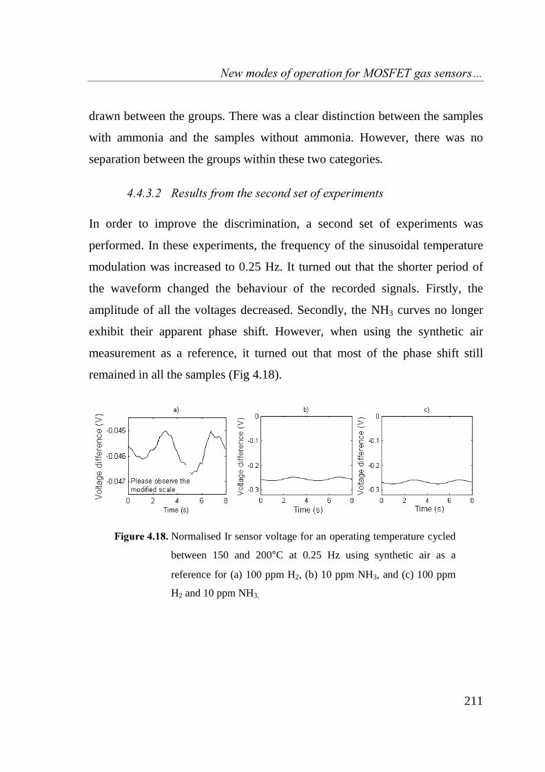
1HZPRGHVRIRSHUDWLRQIRU026)(7JDVVHQVRUV«
211
drawn between the groups. There was a clear distinction between the samples
with ammonia and the samples without ammonia. However, there was no
separation between the groups within these two categories.
5HVXOWVIURPWKHVHFRQGVHWRIH[SHULPHQWV
In order to improve the discrimination, a second set of experiments was
performed. In these experiments, the frequency of the sinusoidal temperature
modulation was increased to 0.25 Hz. It turned out that the shorter period of
the waveform changed the behaviour of the recorded signals. Firstly, the
amplitude of all the voltages decreased. Secondly, the NH3 curves no longer
exhibit their apparent phase shift. However, when using the synthetic air
measurement as a reference, it turned out that most of the phase shift still
remained in all the samples (Fig 4.18).
)LJXUH Normalised Ir sensor voltage for an operating temperature cycled
between 150 and 200°C at 0.25 Hz using synthetic air as a
reference for (a) 100 ppm H2, (b) 10 ppm NH3, and (c) 100 ppm
H2 and 10 ppm NH3.

PAPER IV
212
The data from these measurements were processed and visualised in PCA
plots as for the first measurements. The changed frequency of the temperature
modulation did not improve the separation between the groups.
5HVXOWVIURPWKHWKLUGVHWRIH[SHULPHQWV
In the third set of experiments, the temperature range was 100 to 200°C and
the frequency 0.01 Hz. The extended temperature range was expected to
increase the amount of information obtained from the reactions at the sensor
surface. They would therefore yield better discrimination between the gas
mixtures. However, the voltage curves from these experiments looked almost
identically as in Figure 4.15. Most of the features from the first set of
experiments seemed to be preserved. Normalised sensor voltages when using
synthetic air as a reference signal can be seen in Figure 4.19.
)LJXUH Normalised sensor voltages for an operating temperature cycled
between 100 and 200°C at 0.01 Hz using synthetic air as a
reference for a) 100 ppm H2 b) 10 ppm NH3 and c) 100 ppm H2
and 10 ppm NH3.
The data from these experiments were visualised in PCA plots in a manner
similar to the two earlier data sets. The PCA plot that was based on discrete

1HZPRGHVRIRSHUDWLRQIRU026)(7JDVVHQVRUV«
213
samples from the time domain did not show any improvements with regard to
the ability to discriminate between the gas mixtures (Fig. 4.20a). However, a
separation was obtained between the groups of measurements that had been
Fourier transformed. The separation was good enough to make it possible to
draw straight lines between the gas mixtures, as can be seen in Figure 4.20b.
The differences between these groups of measurements were not large, but the
possibility of drawing lines between the groups implies that the four types of
gases may be separated. However, the number of measurements for each gas
sample was small.
)LJXUH PCA plots from the data in the third set of experiments using (a)
distinct times, and (b) frequencies from the Fourier transform as
variables. : pure synthetic air. : 100 ppm H2. : 10 ppm NH3.
: 100 ppm H2 and 10 ppm NH3.
'LVFXVVLRQ DERXW WHPSHUDWXUH PRGXODWLRQ IRU JDV PL[WXUH
GLVFULPLQDWLRQ
It should be emphasised that the sensor voltage patterns obtained in the cycled
operating mode were different from those from the experiments described in

PAPER IV
214
section 4.4.2, as they were obtained at constant gas concentrations (no sample
gas pulse). This means that the sensor voltage pattern from each experiment
was not dependent on the gas concentration but only on the change in
temperature. It should also be noted that the absolute value of the sensor
voltage, instead of the voltage shift, was used in all these experiments for both
data visualisation and evaluation.
An increase in the temperature decreases the voltage over a sensor operated in
synthetic air. This is due to the electrical effect of the temperature on the
sensor. However, operating the device in a cycled temperature mode in the
presence of a sample gas adds a chemical effect to the sensor voltage. This
effect can be studied separately if the sensor voltage is normalised by
subtracting the sensor voltage in synthetic air is subtracted from the sensor
voltage in the presence of a sample gas (Figs. 4.16, 4.18 and 4.19). In these
experiments, the effect of the sample gas was larger at a low temperature than
at a high temperature. This means that the total coverage of test gas molecules
reached its lowest value at a high temperature. This is in accordance with
previous theoretical findings [18].
The normalised voltage from the sensor decreases when the frequency of the
sinusoidal waveform is increased. This implies that the reactions on the sensor
surface are too slow for this frequency. They do not get enough time to reach
their original value after every period. It was originally thought that this mode
of operation would yield better discrimination between the gas mixtures than a
slower modulation of the temperature, but that result was not achieved.
When studying the samples in the time domain, it is clear that the samples
with 10 ppm NH3 (with or without hydrogen) lie very close to each other. The
same is true for samples without ammonia. The same behaviour is observed in

1HZPRGHVRIRSHUDWLRQIRU026)(7JDVVHQVRUV«
215
the PCA plot. The separation between samples with and without NH3 is very
good, but not within these groups. The small difference between samples of
just synthetic air and both synthetic air and hydrogen implies that not many
hydrogen atoms interfere with the sensor surface. This also explains why the
difference between the NH3 samples is very small. The separation between the
four groups of measurements would probably have been better if the sensors
have been more sensitive to hydrogen.
As could be seen in the PCA plot from the third set of experiments, when
using frequencies as variables, it was possible to draw straight lines between
the four groups of measurements. The separation between the four gas
mixtures was better when frequencies from the Fourier transform were used
instead of distinct times. This may be due to the ability of the FFT to extract
useful information from the signals linked to the shape of the voltage curve.
The time domain yields mostly information about the difference in voltage
between the four curves. However, the distance between the groups in the
corresponding PCA plot was rather small, and more measurements are
required in order to determine the validity of this result. This small distance
and measurements over a long period would probably be sufficient for
differentiating between the four gas mixtures using a pattern recognition
method like PLS or ANN.
4.5 OULOOK FOR OTHER MODES OF OPERATION
Further experiments are underway to evaluate the potential of this new
information, with the aim of applying these modes of operation for specific
gas-sensing applications. With the low-power micromachined MOSFET gas,

PAPER IV
216
new ways of combining different gas sensing principles using different modes
of operation emerge. The results obtained indicate that an “intelligent”
combination of sample and temperature pulses could be used to expand the
information content in sensor response considerably. In the following
paragraphs, a few possibilities will be described.
7KHUPDOFDORULPHWULFVHQVRU
The small thermal mass MOSFET sensor opens up the opportunity to monitor
the heat exchange during exposure to a gas. This parameter could contain
relevant information for applications such as electronic noses [22]. The heat
exchange during gas exposure is produced by chemical reactions between the
analyte gases and the catalytic metals, and/or by the heat transfer by
convection between the sensor surface and the gaseous atmosphere. The latter
is due to the change in thermal conductivity of the ambient atmosphere when
impurities are introduced. It was previously shown that traces of certain gases
could be identified using thermal sensors [23,24].
In our case, it could be useful to combine the heat exchange effect due to
chemical reactions and the field-effect to improve the selectivity of MOSFET
gas sensors. From a practical point-of-view, this means that the power needed
to keep the MOSFET sensor at a constant temperature has to be monitored.
Moreover, an array of hotplates could be designed to combine the low-power
MOSFET with thermal sensors and microcalorimeters. In this way,
information could be obtained about the thermal conductivity of the gases and
the enthalpy changes during the chemical reactions. Depending on the location
of the microcalorimeters and MOSFET sensors, a distributed chemical sensor

1HZPRGHVRIRSHUDWLRQIRU026)(7JDVVHQVRUV«
217
system could be made, in which the gas mixture would be modified along the
flow direction as described in ref. [25].
&RPELQDWLRQ RI WKHUPDOFDORULPHWULF UHVLVWLYH DQG ILHOGHIIHFW
VHQVLQJPHFKDQLVPV
Moreover, a gas-sensitive polymer or a metal-oxide film could replace the
gate material [9,10,12]. In order to obtain more information, the resistance of
the film could be monitored under various gaseous atmospheres to obtain a
resistive, calorimetric, and field-effect gas-sensing device.
2SHUDWLQJDWKLJKWHPSHUDWXUHVHQVLQJDWORZWHPSHUDWXUH
Since the more stable gaseous compounds (e.g. NO2, hydrocarbons) require
higher temperatures to be decomposed by the catalytic metals, another mode
of operation to investigate would be pulsing of the device temperature at
temperatures higher than the working temperature of the transistors (>200°C).
As an example, at higher temperatures hydrocarbons would in general be
decomposed to release hydrogen, which diffuses through the catalyst layer to
reach the metal/insulator interface, where they absorb to form electric dipoles
[11]. By cooling the temperature rapidly to a normal operating temperature
(140-170°C), the signal given by the MOSFET gas sensor could contain
information about these compounds. The desorption of the adsorbed hydrogen
is in most cases slow enough to allow a sufficient amount of hydrogen to
remain after the cooling period [15]. Typical recovery time constants of the
devices at 140-170°C are of the order of 1-10 s (see Fig. 4.12).

PAPER IV
218
6HOIKHDWLQJPRGHRIRSHUDWLRQ
The low-thermal mass of these devices means that they could be used as self-
heating MOSFET gas sensors. The MOSFET could be used as heater and as
field-effect gas sensor at the same time. However, it would be harder to
separate the thermal and field effects in this operational mode, since both have
a direct influence on MOSFET electrical parameters. Considering the actual
design, high voltages would also be needed to meet the power requirement (90
mW / 4 = 22.5 mW per MOSFET) and to keep the MOSFET drain current as
low as possible. Some additional drift problems might appear. To lower the
power consumption, more precise microelectronics and micromachining
processes could be used to scale down the MOSFET and the silicon island [6].
Another way to accomplish this would be to use the silicon-on-insulator (SOI)
technology as proposed in the next paragraph.
6LOLFRQRQLQVXODWRUWHFKQRORJ\
The use of SOI technology allows the fabrication of micro-hotplates with a
reduced silicon island thickness. We have shown that the power consumption
and the thermal time constant could be reduced by at least a factor 2 and 5,
respectively, for the same array on micromachined SOI substrates [26].
Moreover, MOSFETs made on SOI could operate at higher temperatures, up
to 300-350°C [27]. Concerning the self-heating mode, the MOSFETs on SOI
could be thermally isolated by the local oxidation of silicon (LOCOS). They
could therefore be locally self-heated, in contrast to devices made on standard
silicon, in which the whole silicon island is heated.

1HZPRGHVRIRSHUDWLRQIRU026)(7JDVVHQVRUV«
219
4.6 CONCLUSION
A low-power micromachined device allows new modes of operation for
MOSFET gas sensors. The working temperature of the sensor can be
modulated with a time constant smaller than 100 ms. Modulation of the
temperature during gas exposure modifies the kinetics associated with gas
response mechanisms. The different response patterns obtained in these modes
of operation depend on the analyte sensed and on the catalytic sensing film.
A pulse of the sensor temperature after gas exposure can reduce its recovery
time under specific operating conditions. A competition between the
adsorption of chemical species from the outer to the inner surface, and their
desorption from this inner surface, was suggested as an explanation of the
sensor response behaviour. Cycling the temperature can allow discrimination
between different gas mixtures, with effective resolution at a temperature
modulation of ‘low’ frequency and large amplitude. The data were Fourier
transformed before the evaluation was done. Further experiments are
underway to evaluate further the potential use of these effects, with the aim of
applying these modes of operation for specific gas sensing applications.
Other possible modes of operation were discussed. The small thermal mass
could allow monitoring of the heat exchange during gas exposure, increasing
the amount of information obtained from MOSFET gas sensors. SOI
technology was also suggested as a good candidate to improve the
performance of MOSFET gas sensors, by allowing higher temperatures of
operation, lower power consumption, and smaller thermal time constants.

PAPER IV
220
4.7 ACKNOWLEDGEMENTS
This work was done in collaboration with the Swedish Sensor Centre (S-
SENCE) and Applied Sensor (former NST), both located in Linköping,
Sweden. We wish to thank AppliedSensor and the Fonds pour l’aide aux
Chercheurs et à la Recherche (FCAR), from Quebec Government, for their
financial support. We are grateful to the IMT-samlab, Institute of
Microtechnology, Neuchâtel, Switzerland, and the S-SENCE technical staffs
respectively for technical support in the fabrication, and for the
characterisation of these devices. We would like to thank Dr. Per Martensson
and Tomas Eklöv from AppliedSensor, and Dr. Anita Lloyd-Spetz, Dr. Mats
Eriksson and Martin Holmberg from S-SENCE for useful discussions.
4.8 REFERENCES
[1] I. Simon, N. Barsan, M. Bauer, and U. Weimar, “Micromachined metal oxide gas
sensors: Opportunities to improve sensor performance”, Sensors and Actuators, B
73, pp. 1-26, 2001.
[2] R.P Lyle, H.G. Hughes, and D. Walters, “Micromachined silicon CO gas sensors”,
in Conf. Proc. Microstructured and microfabricated systems III, 191st ECS
Meeting, pp. 188-198, 1997.
[3] A. Heilig, N. Barsan, U. Weimar, M. Scheweizer-Berberich, J.W. Gardner and W.
Göpel, “Gas identification by modulating temperatures of SnO2-based thick film
sensors”, Sensors and Actuators, B 43, pp. 45-51, 1997.
[4] G. Faglia, E. Comini, A. Cristalli, G. Sberveglieri, and L. Dori, “Very low power
consumption micromachined CO sensors”, Sensors and Actuators, B55, pp.140-
146, 1999.

1HZPRGHVRIRSHUDWLRQIRU026)(7JDVVHQVRUV«
221
[5] A.P. Lee and B.J. Reedy, “Temperature modulation in semiconductor gas sensing”
Sensors and Actuators, B 60, pp. 35-42, 1999.
[6] D. Briand, H. Sundgren, B. van der Schoot, I. Lundström, and N.F. de Rooij. A
low-power micromachined MOSFET gas sensor, Journal of
Microelectromechanical Systems, 9(3), pp. 303-308, 1999.
[7] D. Briand, B. van der Schoot, H. Sundgren, L.-G. Ekedahl, I. Lundström, and N.
F. de Rooij, “New response patterns for MOSFET gas sensors using low-power
devices”, in Conf. Proc. of Eurosensors XIV, pp. 737-740, 2000.
[8] H. Wingbrant, 'The effect of temperature modulation on a low-power MOSFET
gas sensor', diploma work LITH-IFM-Ex-942, Linköping University, 2001, 52 pp.
[9] M.G.H. Meijerink, M. Koudelka-Hep, N.F. de Rooij, D.J. Strike, W. Olthuis, and
P. Bergveld, “Gas-dependent field effect transistor with an electrodeposited
conducting polymer gate contact”, Electrochemical and Solid-State Letters, 2, pp.
138-139, 1999.
[10] S.K Andreeva and L.I. Popova, “Modelling the gas-sensing behaviour of SnO2-
gate FETs”, Sensors and Actuators, B 19, pp. 540-542, 1994.
[11] I. Lundström and L.-G. Peterson, “Chemical sensors with catalytic metal gates”, J.
Vac. Sci. Technol., A 14, pp. 1539-1545,1996.
[12] J.A. Covington, J.W. Gardner, D. Briand, and N. F. de Rooij, “A polymer gate
FET sensor array for detecting organic vapours”, Sensors and Actuators, B 77, pp.
155-162, 2001.
[13] I. Lundström, S. Shibaraman, C. Svensson, and L. Lundkvist, “A hydrogen-
sensitive MOS field-effect transistor’, Applied Physics Letters, 26 (2), pp. 55-57,
1975.
[14] I. Lundström, T. Ederth, H. Kariis, H. Sundgren, A. Lloyd Spetz, and F. Winquist,
“Recent developments in field-effect gas sensors”, Sensors and Actuators, B 23,
pp. 127-133, 1995.
[15] L.-G. Ekedahl, M. Eriksson, and I. Lundström, “Hydrogen sensing mechanisms of
metal-insulator interfaces”. Accounts of Chemical Research, 31, pp. 249-256,
1998.

PAPER IV
222
[16] M. Johansson, I. Lundström, and L.-G. Petersson, “Kinetic modelling of the H2-O2
reaction on Pd and of its influence on the hydrogen response of a hydrogen
sensitive Pd metal-oxide-semiconductor device”, Surface Science, 350, pp. 91-
102, 1996.
[17] M. Johansson, I. Lundström, and L.-G. Ekedahl, “Bridging the pressure gap for
palladium metal-insulator-semiconductor hydrogen sensors in oxygen containing
environments”, Journal of Applied Physics, 84 (1), pp. 44-51, 1998.
[18] L.-G. Petersson, H.M. Dannetum, J. Fogelberg, and I. Lundström, “Hydrogen
adsorption states at the external and internal palladium surfaces of a palladium-
silicon dioxide-silicon structure”, Journal of Applied Physics, 58 (1), pp. 404-413,
1985.
[19] F. Schoucair, W. Hwang, and P. Jain, “Electrical characteristics of large scale
integration (LSI) MOSFETs at very high temperatures, Part I: Theory”,
Microelectronics and Reliability, 24 (3), pp. 465-485, 1984.
[20] R.G. Brereton, “Fourier transform: use, theory and applications to spectroscopic
and related data”, Chemometrics and Intelligent Laboratory Systems, 1, pp. 17-31,
1986.
[21] K.R. Beebe, R.J. Pell, and M.B. Seasholtz, Chemometrics – A practical guide,
New York, Chichester, Wiley, USA, 1998.
[22] J. Lerchener, D. Caspary, and G. Wolf, “Calorimetric detection of volatile organic
compounds”, Sensors and Actuators, B 70, pp. 57-66, 2000.
[23] C.K. Saul and J.N. Zemel, “Diode-based microfabricated hot-plate sensor”,
Sensors and Actuators, A 65, pp. 128-135, 1998.
[24] M.A. Gajda and H. Ahmed, “Applications of thermal silicon sensors on
membranes”, Sensors and Actuators, A 49, pp. 1-9, 1995.
[25] T. Eklöv and I. Lundström, “Gas mixture analysis using a distributed chemical
sensors system”, Sensors and Actuators, B 57, pp. 274-282, 1999.

1HZPRGHVRIRSHUDWLRQIRU026)(7JDVVHQVRUV«
223
[26] D. Briand, O. Guenat, B. van der Schoot, T. Hirata, and N.F. de Rooij, “Micro-
hotplate, a useful concept for gas-sensing, fluidics and space applications”, in
Conf. Proc. of Microfabricated systems and MEMS V, 198th ECS Meeting, pp.
151-158, 2000.
[27] J.P. Colinge, Silicon on insulator technology: materials to VLSI, 2nd Ed. Kluwer
academic publisher, 1997, 272 pp.
[28] D. Briand, H. Sundgren, B. van der Schoot, I. Lündström, and N.F. de Rooij,
“Thermally isolated MOSFET for gas-sensing application”, IEEE Electron Device
Letters, 22(1), pp. 11-13, 2001.


225
33DDSSHHUU99


3XEOLVKHGLQ&RQI3URF2I
,QW&RQIRQ0RGHOOLQJDQG
6LPXODWLRQRI0LFURV\VWHPV6DQ'LHJR&DOLIRUQLD86$
0DUFKSSPDQXVFULSWLQSUHSDUDWLRQ 227
TTHHEERRMMAALL OOPPTTIIMMIISSAATTIIOONN OOFF MMIICCRROO--HHOOTTPPLLAATTEESS
HHAAVVIINNGG AA SSIILLIICCOONN IISSLLAANNDD
Danick Briand, Stephan Heimgartner, *Marc-Alexis Grétillat,
Bart van der Schoot, and Nicolaas F. de Rooij
Institute of Microtechnology, University of Neuchâtel,
P.O. Box 3, CH-2007 Neuchâtel, Switzerland *currently at Intersema Sensoric SA, Bevaix, Switzerland
ABSTRACT
Thermal measurements and electrothermal simulations (FEM) were performed
in the aim of optimising the power consumption and the temperature
distribution of micro-hotplates for gas-sensing applications. A silicon island
was added underneath the micro-hotplate’s membrane to improve the
temperature distribution of drop-coated metal oxide gas sensors and to
thermally isolate MOSFET gas sensors. The temperature distribution over the
sensing area and the power consumption depend on the silicon island
thickness, which was optimised for both applications using the software
MEMCAD from Microcosm Technologies. The thermal conductivity of
silicon and dielectric membrane, the operating temperature, the geometry and
the area of the heater, and the processing of the silicon island were considered

PAPER V
228
in the optimisation process. The thickness of the silicon island was optimised
to ensure a good temperature distribution over the gas-sensing area for metal-
oxide and MOSFET gas sensors with specific geometry.
5.1 INTRODUCTION
Micro-hotplates are of great interest in the gas sensor field since they allow
reduction of the power consumption and new modes of operation [1-3]. The
main device characteristics which require optimisation are the power
consumption, the temperature distribution over the sensing area, and the
device robustness. They operate generally at high temperatures (i.e. 200-
450°C) and heat losses are generated by conduction through the membrane, by
radiation and by convection in the surrounding atmosphere. Different authors
have reported on the modelling of the thermal behaviour of micro-hotplates
[4-7]. In this paper, the focus is on the optimisation, based on finite element
modelling (FEM), of the power consumption of micro-hotplates having a
silicon island with the aim of achieving a uniform temperature distribution
over the sensing area.
We have recently reported on fabrication and characterisation of micro-
hotplates for gas-sensing applications [8,9]. A 10-µm thick silicon island was
added underneath the micro-hotplate’s membrane, using a two-step bulk
micromachining process, to improve the temperature distribution of drop-
coated metal-oxide gas sensor. The design also allowed the integration of
electronic devices and was used to lower the power consumption of MOSFET
gas sensors. Here, we report on thermal measurements and electrothermal
FEM simulations to optimise the thickness of the silicon island, with the aim

7KHUPDORSWLPLVDWLRQRIPLFURKRWSODWHV«
229
of reducing the power consumption of these micro-hotplates and still have a
homogeneous temperature distribution over the gas sensing area. A uniform
temperature over the sensing area would improve the gas sensitivity and
selectivity of the sensor. A decrease of the silicon island thickness would
facilitate the use of standard etch stop techniques for its fabrication.
A FEM simulator is a useful tool to determine the thermal behaviour of these
devices. So far, the main CAD packages used for this purpose were ANSYS
[10,11], SESES [12], COSMOS [13], and SOLIDIS-ISE [14]. In this work,
the silicon island thickness was optimised using the MEMCAD (4.8) FEM
simulator from Microcosm Technologies, Inc [15]. The Mechanical-Electro-
Thermal module, MemETherm, was used to simulate the thermal behaviour of
the devices. This Joule heating module computes the thermal and electrical
potential field distributions resulting from an applied voltage or current
through a resistive element. The mechanical coupling was not included in the
simulations, though this could be of interest when designing thermal actuators
[16]. The simulation manager, SimMan, was used to investigate the influence
of silicon island thickness and thermal conductivity on the thermal properties
of the micro-hotplates. Infrared (IR) thermal measurements were performed,
and the results combined with those from the simulator to determine the
physical parameters necessary for the simulations.

PAPER V
230
5.2 DESIGN AND FABRICATION
0LFURKRWSODWHVIRUPHWDOR[LGHVHQVRUV
The micro-hotplates for the metal-oxide gas sensors consisted of a heater
sandwiched in between a membrane and an insulator, on top of which sensing
electrodes were integrated. A low-stress LPCVD silicon nitride film was used
as membrane and insulator, which thermally isolates the heated sensing area
from the silicon chip frame as illustrated in Figure 5.1.
/3&9'6LQLWULGH
PHPEUDQHP
6L
P
RUPP
+HDWHU
(OHFWURGHV
2SWLRQDOSDVVLYDWLRQ
/3&9'6LQLWULGH/3&9'6LQLWULGH
LQVXODWRUP
6LLVODQG
RUP
)LJXUH Micro-hotplate with a silicon island for metal-oxide gas sensors.
A two-step silicon bulk micromachining process was used to release the
dielectric membrane and to define the 10-µm thick silicon island. The
thickness was limited at 10 µm since the fabrication process does not provide
precise control over the remaining thickness of the silicon island remaining
after the second etching step. The heater (100 Ω at 0°C) and the electrodes
(sensing area) were made of platinum (TCR=0.00185/°C). More details
concerning the design and fabrication of these micro-hotplates with and
without silicon island are presented in Ref. [8].

7KHUPDORSWLPLVDWLRQRIPLFURKRWSODWHV«
231
The gas sensitivity of a metal-oxide sensor to a specific reducing or oxidising
gas is spread over a certain temperature range. Since the electrodes are
completely covered with the metal-oxide, a temperature gradient as small as
possible is needed over the whole sensing area to improve their selectivity. In
the case investigated here, a temperature gradient of less than 10°C is
considered as ideal. Moreover, these micro-hotplates can withstand operation
at high temperatures (up to 700°C), and allow the annealing “on chip” of the
gas-sensitive material used in the drop-coating process [8]. Therefore, the
temperature distribution over the gas-sensing area is an important parameter to
optimize, so that the gas-sensitive material can be annealed in the same way as
in a belt oven, where temperature gradients are minimised. With an optimized
temperature gradient for the hotplate, it should be possible to achieve the same
gas-sensing characteristics using both annealing techniques.
0LFURKRWSODWHVIRU026)(7VHQVRUV
The micro-hotplates with thermally isolated Gas-sensitive Field-Effect
Transistors (GasFETs) also have a membrane made of low-stress LPCVD
nitride, which was released using a two-step silicon micromachining process
as described above [8]. An array of 4 MOSFET gas sensors was located in the
silicon island, thermally isolated from the chip frame (Fig. 5.2) [9].
The array was surrounded by a heater laid out in a U-shape. The heater
resistor was made either of doped silicon or evaporated platinum. A diode was
used as temperature sensor. The metallisation was made of aluminium and
covered with a PECVD silicon oxynitride film. Windows were opened over
the MOSFET gate oxides and gas-sensitive catalytic metals, such as Ir, Pt and

PAPER V
232
Pd, were deposited to form the GasFETs. Since many sensor arrays can be
used at different temperatures, as in electronic noses, the temperature gradient
between the 4 sensing areas covered by the catalytic metals (size of 60 70
µm2) has to be minimized. A temperature gradient less than 10°C has to be
reached, 5°C is considered as an ideal value.
)LJXUH Schematic cross-sectional view of a micro-hotplate for MOSFET
gas sensors. The electronic components are located in a silicon
island thermally isolated from the silicon chip.
5.3 EXPERIMENTAL
&KDUDFWHULVDWLRQ
The device temperature was measured using an infrared (IR) camera AVIO
2100, with a pixel resolution of 12.5 20 µm2. IR thermal measurements of
the micro-hotplates were performed in both an ambient atmosphere and in
vacuum. The dependence of the resistance on the applied voltage and on the

7KHUPDORSWLPLVDWLRQRIPLFURKRWSODWHV«
233
maximum temperature at the center of the heater under these conditions was
monitored. Then, from these results, the temperature coefficient of the
resistance (TCR) was calculated. Finally, using the value of the resistance at
room temperature, and the TCR, the relation between the power consumption
and the temperature was obtained. This way, the problem of the determination
of material emissivity was avoided.
Because of the camera pixel size being similar to heater width and this
difficulty of determining a value of emissivity for the materials in the different
regions, precise mapping of the temperature over the whole heated area was
rather difficult. It was concluded that simulations could yield more reliable
results about the temperature distribution if the thermal properties of the
materials were defined.
2SWLPLVDWLRQDQGVLPXODWLRQ
For the metal-oxide gas sensors, the temperature distribution over the sensing
area of micro-hotplates without silicon islands was first investigated. Different
heater geometries such as simple and double meander were studied (Fig 5.5).
It was found that the power consumption was lowered by adjusting the
membrane and heater size, but this was not the main goal of the work
presented here. As mentioned before, the focus was on the optimisation of the
hotplates having a silicon island. Membranes having two sizes were
considered: 1.0 1.0 mm2 and 1.5 1.5 mm2, with a heater/sensing area of
450 450 µm2 and 750 750 µm2, respectively. In the case of the MOSFET
gas sensors, the geometry was fixed, with 1.5 1.5 mm2 for the membrane

PAPER V
234
and 750 750 µm2 for the active area, since the technology used in house for
the processing did not allow for a higher density of integration [8].
The thickness of the silicon island was optimised for both types of micro-
hotplates staking hotplate geometry and fabrication into account. Simulations
were performed to determine the minimum thickness of silicon necessary to
have a uniform temperature distribution over the sensing area. The boundary
conditions and the parameters were set as follows:
• The chip frame temperature was set at 30°C in accordance with the IR
observations;
• The heat was dissipated by convection in the gaseous atmosphere on the
front (h = 250 W•m-2K-1) and backside (h = 125 W•m-2K-1) surfaces of the
membrane [12];
• The thermal conductivity (k) of the silicon rich LPCVD nitride film was set
in the range of 3.2–22 W•m-1K-1, of platinum at 71 W•m-1K-1, and of
silicon between 50 and 150 W•m-1K-1, depending on its level of doping
[11,12,18-20];
• An operating temperature in the range of 200-400°C was considered for the
metal-oxide sensors;
• A maximum operating temperature of 200°C was considered for the
MOSFET sensors;
• To simplify the simulation, the heater was made of platinum sandwiched in
between nitride films for both types of devices.
• The temperature gradient in the z direction and the radiation were
considered negligible [3,12];

7KHUPDORSWLPLVDWLRQRIPLFURKRWSODWHV«
235
• The forced gas flow, used for instance in electronic noses, was assume to
have no influence on the temperature distribution [17];
• The dependence of the thermal conductivity on temperature was not
considered;
The different designs on which the simulations were performed are described
in Table 5.1. S1 and S2Si correspond to two types of metal-oxide micro-
hotplate, without and with a silicon island, respectively. S2Si without silicon
island is named S2. S3Si is the only design investigated for the MOSFET
micro-hotplate.
7DEOH The different designs simulated for metal-oxide and MOSFET
micro-hotplates with and without silicon island.
S1 S2Si* S3Si
Sensor type Metal-oxide MOSFET
Membrane area (mm2) 1.0 1.0 1.5 1.5 1.5 1.5
Sensing area (µm2) 450 450 750 750 750 750
Si-island area (µm2) –––––––– 800 800 800 800
Membrane thickness (µm) 0.25 + 0.75 0.25 + 0.25
Pt-heater geometry Simple and double meander
U-shape
Pt-heater thickness (µm) 0.25
*S2Si without silicon island is named S2

PAPER V
236
5.4 RESULTS AND DISCUSSION
7KHUPDOPHDVXUHPHQWV
The thermal measurements were performed on micro-hotplates for metal-
oxide and MOSFET sensors [8,9]. Here, the results are presented only for the
micro-hotplates for metal-oxide sensors since there was no variation of the
dimensions for the MOSFET sensors (design S3Si only, see Table 5.1).
At an operating temperature of 300 °C, the power consumption of the micro-
hotplates without silicon islands was of about 50 mW for the 1.0 1.0 mm2
design (S1) and of about 75 mW for the 1.5 1.5 mm2 (S2). The lower power
consumption of the micro-hotplates with a membrane area of 1.0 1.0 mm2
could be explained by their smaller heating area, which reduces the absolute
heat lost by convection. A way to optimise the power consumption would be
to minimise the heating area in relation to the membrane size as shown in refs.
[3,10-12]. In the review published by Simon et al. [3], ratios of 2.6 and 3.0,
corresponding to the radius of the heated area to the radius of the membrane,
are given for minimum power consumption. In our case, this would mean
combining a heating area of 500 500 µm2 with a membrane size of 1.5
1.5 mm2. However, in a commercial production, a compromise between the
power and the density of integration has to be reached.
The power consumption for micro-hotplates having a 10-µm thick silicon
island (S1Si and S2Si) was about 45% higher at an operating temperature of
300°C. At a given operating temperature, the heat dissipated while
maintaining a uniform temperature over the sensing area would be lowered by
optimising the thickness of the silicon island to be less than 10 µm.

7KHUPDORSWLPLVDWLRQRIPLFURKRWSODWHV«
237
In the case of the metal-oxide micro-hotplates without silicon islands (S1, S2),
the thermal observations indicated that the temperature distribution over the
sensing area was more homogeneous for the double meander heater than for
the simple meander (Fig. 5.3).
500 1000150
200
250
300
350
Tem
per
atu
re (
°C)
Distance (um) (a)
1000 1500 2000150
200
250
300
350
Tem
per
atu
re (
°C)
Distance (um) (b)
)LJXUH Cross-section of the temperature distribution for a metal-oxide
micro-hotplate with (a) simple and (b) double meander heaters
(S1), from IR thermal measurements.

PAPER V
238
The hollows in the Figure 5.3 are due to the difference of emissivity value
between the arms of the platinum heater and the silicon nitride membrane. The
value of emissivity could not be adjusted locally on the system used for the
measurements and therefore the graphs in Figure 5.3 are representative of the
two different heater designs.
The thermal measurements also suggested that the silicon plug added
underneath the membrane improves the temperature distribution over the
sensing area as shown in Figure 5.4. The curve obtained presented a smoother
shape than those in Figure 5.3, taken on devices without silicon island, since
the radiation intensity measured by the IR-camera is mainly coming from the
silicon island.
0 500 1000 1500 2000
200
220
240
260
280
300
320
340
360
Tem
per
atu
re (
°C)
Distance (um)
)LJXUH Cross-section of the temperature distribution over the sensing area
for a metal-oxide micro-hotplate with a simple meander heater
and a silicon island (S2Si), obtained by IR thermal measurements.

7KHUPDORSWLPLVDWLRQRIPLFURKRWSODWHV«
239
)(0VLPXODWLRQV
0LFURKRWSODWHVZLWKRXWVLOLFRQLVODQG
The FEM simulations confirmed the indications obtained from the thermal
measurements about the temperature distribution for the different heater
designs. The temperature distribution over the sensing area was more
homogeneous for the double meander heater than for the simple meander as
shown in Figure 5.5 and in Table 5.2 for the 1.0 1.0 mm2 design (S1).
520
560
600
640
680
720
-300 -200 -100 0 100 200 300
Distance (Pm)
Tem
per
atu
re (K
)
DM heater
SM heater
)LJXUH Temperature distribution at 400°C for the simple (SM) and double
meander (DM) heaters on a membrane of 1.0 1.0 mm2
(S1, knitride =22 W•m-1K-1).
SM DM

PAPER V
240
At an operating temperature of 400°C (knitride =22 W•m-1K-1), the temperature
gradient between the center and the edge of the sensing area is 100°C and 23
°C for the simple and double meander, respectively (Fig. 5.5 and Table 5.2).
Therefore, for a metal-oxide micro-hotplate without silicon island, the double
meander heater definitely provides the best performance. The double meander
structure gives more flexibility in the design of the heater It can be adapted to
different thermal conductivity of the membrane material (silicon nitride in this
case) by changing the width of its elements and/or the distance between them.
7DEOH Influence of the operating temperature (200, 300 and 400°C) on
the temperature gradients of simple and double meander heaters
on a 1.0 × 1.0 mm2 membrane (S1).
6LPSOHPHDQGHUKHDWHU
knitride=22 W•m-1K-1
6LPSOHPHDQGHUKHDWHU
knitride=3.2 W•m-1K-1
V [V] Tmax [°C] ∆Tmax [°C] V [V] Tmax [°C] ∆Tmax [°C]
2.25 207 45 1.70 204 47
2.75 297 75 2.10 299 67
3.25 405 100 2.45 398 91
'RXEOHPHDQGHUKHDWHU
knitride=22 W•m-1K-1 'RXEOHPHDQGHUKHDWHU
knitride=3.2 W•m-1K-1
V [V] Tmax [°C] ∆Tmax [°C] V [V] Tmax [°C] ∆Tmax [°C]
2.50 200 10 1.70 198 8
3.15 302 15 2.20 315 15
3.70 406 23 2.50 398 20
Figures 5.6, as well as the results given in Table 5.2, show that the
temperature gradient on the sensing area depends also on the temperature of
operation. The temperature gradient is larger for a higher operating

7KHUPDORSWLPLVDWLRQRIPLFURKRWSODWHV«
241
temperature. Moreover, in the case of the designs considered here,
maintaining the ratio of heater area radius to membrane radius constant, the
size of the heater area influenced the temperature gradient over the sensing
area for the metal-oxide hotplate, as presented in Figure 5.7. The gradient was
larger for the larger design, S2, than for S1.
400
450
500
550
600
650
700
-400 -200 0 200 400
Distance (um)
Tem
per
atu
re (
K)
200°C
300°C
400°C
(a)
400
450
500
550
600
650
700
-400 -200 0 200 400
Distance (um)
Tem
per
atu
re (
K)
200°C
300°C
400°C
(b)
)LJXUH Influence of the operating temperature on the temperature
gradient between the centre and the edge of the sensing area for
the metal-oxide micro-hotplate (S1, knitride = 22 W•m-1K-1) with
(a) simple meander and (b) double meander heater

PAPER V
242
20
40
60
80
100
120
100 200 300 400 500
Operating temperature (°C)
'T
(°C
)
S1S2
)LJXUH Influence of the heater area (S1 and S2) on the temperature
gradient between the centre and the edge of the sensing area for
the metal-oxide micro-hotplate with a simple meander heater
(knitride=22 W•m-1K-1).
Depending on the technology and applications, different types of heater
geometry have been proposed during the last years [10,12,21-23]. However, to
our knowledge, a temperature gradient lower than 10°C has not been reported
so far for closed-membranes. Since the temperature gradient between the
center and the edge of the sensing area can reach a value of about 110°C for a
simple meander heater operating at 400°C on a 1.5 1.5 mm2 membrane (S2)
(see Figure 5.7), this was considered as our worse case to optimise. A 10-µm
thick silicon island (k=100 W•m-1K-1) was added underneath the membrane of
this design (S2Si, simple meander heater) to improve the temperature
homogeneity over the sensing area.

7KHUPDORSWLPLVDWLRQRIPLFURKRWSODWHV«
243
0LFURKRWSODWHVZLWKVLOLFRQLVODQG
A 10-µm thick silicon island was added to the metal-oxide micro-hotplate
with a simple meander heater (S2Si) with the hope of reaching a temperature
gradient less than 10°C over the heating/sensing area. The FEM simulations
confirmed the experimental results presented in Figure 5.4. Using this design,
a uniform temperature distribution (< 5°C) over the sensing area was obtained
all over the silicon island surface as shown in Figure 5.8a. Another interesting
point is that temperature distribution was found to be almost independent of
the heater geometry. This is evident in Figure 5.8b which shows the
homogeneous temperature distribution over the sensing area for a U-shaped
heater on a silicon nitride membrane with the silicon island underneath.
(a) (b)
)LJXUH FEM simulations of a micro-hotplate with a silicon island (S2Si,
S3Si) for (a) simple meander, and (b) U-shape heater (z-axis x 50,
temperature = 300°C, kSi= 100 W•m-1K-1, knitride= 3.2 W•m-1K-1).
Therefore, the heater and the electrodes (Pt) could be defined in one
fabrication step using the same mask level [23].

PAPER V
244
Moreover, a semiconducting heater having a U-shape was adopted for the
MOSFET sensor (S3Si). This heater geometry gives more flexibility in the
layout, which is an important issue due to the high number of electrical
connections for this device.
2SWLPLVDWLRQRIWKHVLOLFRQLVODQGWKLFNQHVV
The optimum silicon island thickness to minimise the power consumption and
maintain a uniform temperature distribution over the sensing area was
determined by simulation. The metal-oxide sensor with a simple meander
heater (S1Si and S2Si) and a MOSFET sensor with a U-shaped heater (S3Si)
were considered. Different parameters, such as the heater area, operation
temperature, thermal conductivity of the materials used, and silicon island
fabrication, were taken into account.
+HDWLQJDUHDDQGRSHUDWLQJWHPSHUDWXUH
As presented in Figure 5.7 for metal-oxide micro-hotplates, the heater area can
have an influence on the temperature gradient depending on the design. The
gradient was larger for the larger design, S2, than for S1. Therefore, the
silicon island thickness was optimised for the design S2Si, with assumption
that the results could be transferred to S1 with slight improvement. The
thickness of the silicon island for the MOSFET micro-hotplates was
minimised for the only design considered here, S3Si.
Figures 5.6, as well as the results given in Table 5.2, show that the
temperature gradient on the sensing area depends also on the temperature of
operation. The temperature gradient is larger for a higher operating

7KHUPDORSWLPLVDWLRQRIPLFURKRWSODWHV«
245
temperatures. Indeed, the temperature of operation of metal-oxide gas sensors
depends on the nature of the gas to be detected and typically varies from
200°C (e.g. NO2) to 400°C (e.g. CH4). This effect is less important for
MOSFET sensors since their temperature of operation is limited to 225°C, due
to the appearance of leakage currents at higher temperatures. The simulations
to optimise the silicon island thickness were performed at a specific operating
temperature of 300°C and 200°C for the metal-oxide and MOSFET sensors,
respectively.
0DWHULDOVWKHUPDOFRQGXFWLYLW\
The temperature distribution over the sensing area depends also on the thermal
conductivity of the silicon forming the island, which is related to the
fabrication process. Simulations were performed considering different levels
of doping of the silicon. The thermal conductivity (k) was set at 150 W•m-1K-1
for pure silicon, and at 100 W•m-1K-1 and 50 W•m-1K-1 for doped silicon used
in electrochemical (n-type) and boron (p++) etch stop processes, respectively
[11,20]. The influence of the thermal conductivity of the silicon on the
temperature gradient is shown for the metal-oxide micro-hotplate in Figure
5.9.
Since the thermal conductivity of a thin film is not easy to determine, a low
value of 3.2 W•m-1K-1 (low-stress) and a high value of 22 W•m-1K-1 (standard)
were taken from the literature for the silicon nitride film used as membrane
[11,18]. Its influence on the temperature distribution over the sensing area is
also presented in Figure 5.9. The high value gives a higher temperature
gradient over the sensing area as expected. The micro-hotplates optimised

PAPER V
246
here have a low-stress silicon nitride as membrane. A thermal conductivity of
3.2 W•m-1K-1 was therefore chosen to perform the simulations with the aim of
minimising the silicon island thickness. However, one should be aware that
the value of this parameter should be experimentally determined to confirm
the following results.
0
2
4
6
8
10
12
14
0 50 100 150 200
Silicon thermal conductivity (Wm-1K-1)
Tem
per
atu
re g
rad
ien
t (°C
)
nitride = 3.2 Wm-1K-1 nitride = 22 Wm-1K-1
)LJXUH Influence of the silicon thermal conductivity on the temperature
gradient for metal-oxide micro-hotplates having a silicon island (5
µm thick) and operating at 300°C (S2Si with simple meander
heater, knitride = 3.2 W•m-1K-1 and 22 W•m-1K-1).
2SWLPLVHG VLOLFRQ LVODQG WKLFNQHVV IRU PHWDOR[LGH PLFUR
KRWSODWHV
In the case of metal-oxide sensors, the temperature gradient has to be
optimised to improve the sensitivity and selectivity of the gas sensitive coating
over the electrodes. This means that the temperature gradient has to be

7KHUPDORSWLPLVDWLRQRIPLFURKRWSODWHV«
247
minimised over the entire sensing area. Figure 5.10 shows the influence of the
silicon island thickness on the temperature gradient over the sensing area for a
simple meander heater. A 2.0−2.5-µm-thick silicon island (k = 50 W•m-1K-1)
is enough to reduce the temperature gradient over the sensing area (750 750
µm2) to a value of about 10°C. Therefore, the two-step silicon bulk
micromachining process used to fabricate the 10 µm-thick silicon island could
be replaced by a high concentration boron etch stop (p++) made by
implantation.
0 200 400 600 800556
558
560
562
564
566
568
570
572
574
576
Tem
per
atu
re (
K)
Distance (Pm)
1.5 um 2.0 um 2.5 um 3.0 um 3.5 um 4.0 um 5.0 um 10.0 um
)LJXUH Temperature distribution over the sensing area (section in the
middle) of a metal-oxide micro-hotplate as a function of the
silicon island thickness (k = 50 W•m-1K-1) for an operating
temperature of 300°C (S2Si with simple meander heater, knitride =
3.2 W•m-1K-1)

PAPER V
248
2SWLPLVHG VLOLFRQ LVODQG WKLFNQHVV IRU PHWDOR[LGH PLFUR
KRWSODWHV
The MOSFET array sensor contains four different sensitive areas (60 70
µm2) that should operate at the same temperature (Fig 5.11). Therefore, the
silicon island thickness has to be minimised with the aim of obtaining a
temperature gradient on individual devices (on 60 70 µm2) and between the
devices that does not exceed 5°CThe array of devices has a symmetric 2 2
configuration and is placed in between the U-shaped heater
Heater
Diode
MOSFET
)LJXUH Photograph of the MOSFET array gas sensor, on which are the
four MOSFETs surrounded by the heater (U-shape) and with the
diode in the middle (temperature sensor).
For a minimum silicon island thickness of 1.5 µm, Figures 5.12 and 5.13 show
that the gradient is less than 5°C on an individual sensor and also between two
sensors in a symmetric position with respect to the heater (the two on the left

7KHUPDORSWLPLVDWLRQRIPLFURKRWSODWHV«
249
or on the right in Fig. 5.11). However, for a given silicon island thickness, a
comparison of Figures 5.12 and 5.13 is necessary to determine thetemperature
gradient between the two sensors on the left and the two on the right on Figure
5.11. It was found that a silicon island (k = 100 W•m-1K-1) with a minimum
thickness of 2.0 µm provides a homogenous temperature for the sensor array.
The temperature gradient is less than 5°C.
0 200 400 600 800
462
464
466
468
470
472
474
476
478
Tem
per
atu
re (
K)
Distance (Pm)
1.0 um 1.5 um 2.0 um 2.5 um 3.0 um 4.0 um 5.0 um 10.0 um
)LJXUH Temperature distribution (cross-section on the two sensors on the
left in Fig. 5.11) over a MOSFET micro-hotplate as a function of
the silicon island thickness (k = 100 W•m-1K-1) for an operating
temperature of 200°C (S3Si with U-shaped heater, knitride = 3.2
W•m-1K-1).

PAPER V
250
An electrochemical etch stop process could be used to fabricate the silicon
island. In this case, a boron etch stop is not suitable since it is not compatible
with the integration of electronic components in the silicon island.
0 200 400 600 800450
455
460
465
470
475
Tem
per
atu
re (
K)
Distance (Pm)
1.0 um 1.5 um 2.0 um 2.5 um 3.0 um 4.0 um 5.0 um 10.0 um
)LJXUH Temperature distribution (cross-section on the two sensors on the
right in Fig. 5.11) over a MOSFET micro-hotplate as a function of
the silicon island thickness (k = 100 W•m-1K-1) for an operating
temperature of 200°C (S3Si with U-shaped heater, knitride = 3.2
W•m-1K-1).
5.5 CONCLUSION
The power consumption and the temperature distribution of micro-hotplates
having a silicon island were optimised by using MEMCAD to simulate their
thermal behaviour. Optimised silicon island thicknesses were determined by

7KHUPDORSWLPLVDWLRQRIPLFURKRWSODWHV«
251
simulation, to improve the temperature distribution over the sensing areas of
low power metal-oxide and MOSFET gas sensors. The specific operating
temperatures, heater geometry and thermal conductivity were considered in
the simulations.
A 10-µm-thick silicon island was found to be suitable for the design of micro-
hotplates with no restrictions introduced by heater geometry. Therefore, the
platinum heater and electrodes for the metal-oxide micro-hotplates could be
defined in one photolithographic step. Optimisation by simulation of the
silicon island thickness to decrease power consumption and facilitate its
fabrication was performed for specific applications. Two-steps silicon bulk
micromachining in KOH to make the silicon island could be replaced by a
boron or an electrochemical etch stop process for metal-oxide and MOSFET
micro-hotplates, respectively.
We are looking at the influence of a thin layer of silicon on the temperature
distribution over the gas sensing area to evaluate the use of silicon-on-
insulator (SOI) substrates. SOI technology provides an integrated etch-stop for
the silicon island in the form of a buried oxide layer. Increased operating
temperatures for of the MOSFET sensors should also be made possible using
this technology.
5.6 ACKNOWLEDGEMENTS
The European program Brite-Euram III (n° BRPR-CT96-0194),
AppliedSensor (former NST, Linköping, Sweden) and the Fonds pour la
formation des Chercheurs et l’Aide à la Recherche (FCAR) from the Quebec
Government have financially supported this project. We are grateful to IMT-

PAPER V
252
samlab, Institute of Microtechnology, University of Neuchâtel, Neuchâtel,
Switzerland, technical staff for the support in the fabrication of the devices.
We would like also to thank Dr. E. Scheid, Laboratory for Analysis and
Architecture of Systems (LAAS), Toulouse, France, for the IR thermal
measurements and Dr. P. Martensson from AppliedSensor, Linköping,
Sweden, and Dr. N. Barsan and A. Krauss, University of Tübingen, Tübingen,
Germany, for helpful discussions.
5.7 REFERENCES
[1] G. Sberveglieri, W- Hellmich, and G. Müller, “Silicon hotplates for metal oxide
gas sensor elements”, Microsystem Technologies, 3, pp.183-190, 1997.
[2] A.P. Lee and B.J. Reedy, “Temperature modulation in semiconductor gas
sensing”, Sensors and Actuators, B 60, pp. 35-42, 1999.
[3] I. Simon, N. Barsan, M. Bauer, and U. Weimar, “Micromachined metal oxide gas
sensors: Opportunities to improve sensor performance”, Sensors and Actuators, B
73, pp. 1-26, 2001.
[4] U. Dibbern, “A substrate for thin-film gas sensors in microelectronic technology”,
Sensors and Actuators, B 2, pp. 63-70, 1990
[5] W. Lang, “Heat transport from a chip”, IEEE Trans. on Electron Devices, 37(4),
pp. 958-963, 1990.
[6] U. Dillner, “Thermal modeling of multilayer membranes for sensors applications”,
Sensor and Actuators, A 41-42, pp. 260-267, 1994.
[7] A. Pike and J.W. Gardner, “Thermal modelling and characterisation of
micropower chemoresistive silicon sensors”, Sensors and Actuators, B 45, pp. 19-
26, 1997.

7KHUPDORSWLPLVDWLRQRIPLFURKRWSODWHV«
253
[8] D. Briand, A. Krauss, B. van der Schoot, U. Weimar, N. Barsan, W. Göpel, and
N.F. de Rooij, “High temperature micro-hotplates for drop-coated gas sensors”,
Sensors and Actuators, B 68, pp. 223-233, 1999.
[9] D. Briand, B. van der Schoot, H. Sundgren, I. Lundström, and N.F. de Rooij, A
low-power micromachined MOSFET gas sensor, Journal of Micro-Electro-
Mechanical Systems, 9(3), pp. 303-308, 2000.
[10] A. Gotz, I. Gràcia, C. Cané, and E. Lora-Tamayo, “Thermal and mechanical
aspects for designing micromachined low-power gas sensors”, Journal of
Micromechanics and Microengineering, 7, pp. 247-249, 1997.
[11] C. Rossi, E. Scheid, and D. Estève, “Theoretical and experimental study of silicon
micromachined microheater with dielectric stacked membranes”, Sensors and
Actuators, A 63, pp. 183-189, 1997.
[12] S. Astié, A.M. Gué, E. Scheid, L. Lescouzères, and A. Cassagnes, “Optimisation
of an integrated SnO2 gas sensor using a FEM simulator”, Sensors and Actuators,
A 69, pp. 205-211, 1998.
[13] M. Dumitrescu, C. Cobianu, D. Lungu, D. Dascalu, A. Pascu, S. Kolev, and A.
van den Berg, “Thermal simulation of surface micromachined polysilicon hot
plates of low power consumption”, Sensors and Actuators, A 76, pp. 51-56, 1999.
[14] L. Chih-Cheng, D. Setiadi, F. Udrea, W. Milne, J.A. Covington, and J.W. Gardner,
“3D therm-electro-mechanical simulations of gas sensors based on SOI
membranes”, in Conf. Proc. of 3rd Int. Conf. on Modeling and Simulation of
Microsystems (MSM’00), pp. 297-300, 2000.
[15] Microcosm Technologies Inc., Development Center, 101 Rogers St., Suite 213,
Cambridge, MA 02142, USA.
[16] D.J. Silversmith, and J.R. Reid, “Joule heating simulations of polysilicon
microactuators”, in Conf. Proc. of 2nd Int. Conf. on Modeling and Simulation of
Microsystems (MSM’99), pp. 613-615, 1999.
[17] P. Mielle, “Managing dynamic thermal exchanges in commercial semiconducting
gas sensors”, Sensors and Actuators, B 34, pp. 533-538, 1996.

PAPER V
254
[18] C.H. Mastrangelo, Y.-C. Tai, and R.S. Muller, “Thermophysical properties of low-
residual stress, silicon-rich, LPCVD silicon nitride films”, Sensors and Actuators,
A 21-23, pp. 856-860, 1990.
[19] R.P. Manginell, D.A. Rosato, D.A. Benson, and G.C. Frye-Mason, “Finite element
modelling of a microhotplate for microfluidic applications”, in Conf. Proc. Of the
2nd Int. Conf. On Modeling and Simulations of Microsystems (MSM’99), pp. 663-
666, 1999.
[20] G. Slack, “Thermal conductivity of pure and impure silicon, silicon carbide, and
diamond” J. Appl. Phys.,35(12), pp. 3460-3466, 1964.
[21] V. Guidi, G.C. Cardinali, L. Dori, G. Faglia, M. Ferroni, G. Martinelli, P. Nelli,
and G. Sberveglieri, “Thin-film gas sensor implemented on a low-power-
consumption micromachined silicon structure” Sensors and Actuators, B 49, pp.
88-92, 1998.
[22] R. Aigner, M. Dietl, R. Katterlober, and V. Klee, “Si-planar-pellistor: designs for
temperature modulated operation“, Sensors and Actuators, B 33, pp. 151-155,
1996.
[23] W.-Y. Chung, J.-W. Lim, D.-D. Lee, N. Miura, and N. Yamazoe, “Thermal and
gas-sensing properties of planar-type micro gas sensor”, Sensors and Actuators, B
64, pp 118-123, 1999.

255
//LLVVWWRRIISSXXEEOOLLFFDDWWLLRRQQVV


257
LLiisstt ooff ppuubblliiccaattiioonnss
Referred articles
D. Briand, H. Windgrant, H. Sundgren, B. van der Schoot, L.-G. Ekedahl, I. Lundström,
and N. F. de Rooij, “New modes of operation for MOSFET gas sensors using low-power
devices”, manuscript in preparation.
D. Briand, S. Heimgartner, M.-A. Grétillat, B. van der Schoot, and N.F. de Rooij, “Thermal
optimisation of micro-hotplates having a silicon island”, manuscript in preparation.
R. Tamadori, J.W. Gardner, A. Krauss, U. Weimar, D. Briand, B. van der Schoot, H.
Sundgren, I. Besnard, P. Barttlet, L. Gier, and S. Cosensa, “A cabin air analyser”,
submitted.
J.A. Covington, J.W. Gardner, D. Briand, and N. F. de Rooij, “A polymer gate FET sensor
array for detecting organic vapours”, Sensors and Actuators, B 77, pp. 155-162, 2001.
D. Briand, H. Sundgren, B. van der Schoot, I. Lündström, and N.F. de Rooij, “Thermally
isolated MOSFET for gas-sensing application”, IEEE Electron Device Letters, 22(1), pp.
11-13, 2001.
D. Briand, B. van der Schoot, H. Sundgren, I. Lundström, and N.F. de Rooij, “A low-power
micromachined MOSFET gas sensor”, Journal of Micro-Electro-Mechanical Systems, 9(3),
pp. 303-308, 2000.

258
D. Briand, A. Krauss B. van der Schoot, U.Weimar, N. Barsan, W. Göpel, and N.F. de
Rooij, “Design and fabrication of high temperature micro-hotplates for drop coated gas
sensors”, Sensors and Actuators, B 68, pp. 223-233, 2000.
O. Renault, D. Briand, G. Delabouglise, J. F. Currie, and M. Labeau, “Integration of a
sensitive material to a silicon-based device for CO detection”, Sensors and Actuators, A 74,
pp. 225-228, 1999.
D. Briand, M. Labeau, J. F. Currie, and G. Delabouglise, “Pd-doped SnO2 thin films
deposited by CVD assisted ultrasonic spraying for gas-sensing: selectivity and effect of
annealing”, Sensors and Actuators, B 48, pp. 395-402, 1998.
Conferences and workshop proceedings
J.W. Gardner, S.M. Lee, D.C. Dyer, P.N. Bartlett, S. Guerin, D. Briand, and N.F. de Rooij,
“Silicon planar microcalorimeter employing nanostructured films”, Tech. Digest of
Transducers’01, Munich, Germany, pp. 820-823, 2001.
D. Briand, O. Guenat, B. van der Schoot, T. Hirata, and N.F. de Rooij, “Micro-hotplate, a
useful concept for gas-sensing, fluidics and space applications”, Conf. Proc. of
Microfabricated Systems and MEMS V, 198th ECS Meeting, pp. 151-158, 2000.
L. Dellmann, T. Akiyama, D. Briand, S. Gautsch, B. Guldimann, P. Luginbuhl, C. Marxer,
U. Staufer, and N. F. de Rooij, “Microsystems for diverse applications using recently
developed microfabrication techniques”, Conf. Proc. SPIE vol. 4176, Micromachined
Devices and Components VI, pp. 16-27, 2000,

/LVWRISXEOLFDWLRQV
259
O. T. Guenat,T. Hirata, D. Briand, P.-A. Clerc, G. Mondin, U. Kroll, and N. F. de Rooij,
“Pneumatic conveyance systems for micro-parts transportation”, Conf. Proc. of the 2nd
International Workshop on Microfactories, pp. 43-46, 2000.
D. Briand, B. van der Schoot, H. Sundgren, L.-G. Ekedahl, I. Lundström, and N. F. de
Rooij, “New response patterns for MOSFET gas sensors using low-power devices”, Proc.
of Eurosensors XIV, pp. 737-740, 2000.
J.A. Covington, J.W. Gardner, C. Toh, P.N. Bartlett, D. Briand, and N.F. de Rooij, “Array
of MOSFET devices with electrodeposited conducting polymer gates for vapour and odour
sensing”, Conf. Proc. of the 7th International Symposium on Olfaction and Electronic Nose,
2000.
D. Briand, M.-A. Gretillat, B. van der Schoot, and N.F. de Rooij, “Thermal management of
micro-hotplates using MEMCAD as simulation tool”, Conf. Proc. of 3rd Int. Conf. on
Modelling and Simulation of Microsystems, pp. 640-643, 2000.
D. Briand, B. van der Schoot and N.F. de Rooij, A. Krauss, U.Weimar, N. Barsan, and W.
Göpel, “High temperature micro-hotplates for drop-coated gas sensors”, Conf. Proc. of
Eurosensors XIII, pp. 703-704, 1999.
D. Briand, B. van der Schoot, S. Jeanneret, P.-A. Clerc, and N.F. de Rooij, H. Sundgren, I,
Grahn, and I. Lundström, “Novel low-power consumption MOSFET array gas sensor”,
Tech. Digest of Transducers’99, pp. 938-941, 1999.
O. Renault, D. Briand, G. Delabouglise, J. F. Currie, and M. Labeau, “Integration of a CO
sensitive film on silicon”, Conf. Proc. of EMRS-Meeting, Symposium: Materials for
Microsystems, 1998.

260
D. Briand, M. Labeau, G. Delabouglise, and J. F. Currie, “Pd-doped SnO2 thin films
deposited by CVD assisted ultrasonic spraying for gas-sensing: selectivity and effect of
annealing”, Conf. Proc. of Eurosensors XI, pp. 451-454, 1997.
D. Briand, G. Delabouglise, A. Lecours, J. F. Currie, and M. Labeau, “Pd-doped SnO2 thin
films for CO detection”, Conf. Proc. of the 2th International Symposium on New Materials
for Fuel Cell and Modern Battery System, Montréal, Canada, July 1997, pp 911-914.
Patent
D. Briand, H. Sundgren, B. van der Schoot, I. Lundström, and N.F. de Rooij, GasFET
devices integrated on micro-machined hotplates and methods for their fabrication,
submitted.