Thermally Aware Design - Electrical and Computer …people.ece.umn.edu/~sachin/jnl/FnT08.pdf ·...
116
Foundations and Trends R in Electronic Design Automation Vol. 2, No. 3 (2007) 255–370 c 2008 Y. Zhan, S. V. Kumar and S. S. Sapatnekar DOI: 10.1561/1500000007 Thermally Aware Design Yong Zhan 1 , Sanjay V. Kumar 2 and Sachin S. Sapatnekar 3 1 Cadence Design Systems, 555 River Oaks Parkway, San Jose, CA 95134, USA, [email protected] 2 Department of Electrical and Computer Engineering, University of Minnesota, Minneapolis, MN 55455, USA, [email protected] 3 Department of Electrical and Computer Engineering, University of Minnesota, Minneapolis, MN 55455, USA, [email protected] Abstract With greater integration, the power dissipation in integrated circuits has begun to outpace the ability of today’s heat sinks to limit the on-chip temperature. As a result, thermal issues have come to the forefront, and thermally aware design techniques are likely to play a major role in the future. While improved heat sink technologies are available, economic considerations restrict them from being widely deployed until and unless they become more cost-effective. Low power design is helpful in controlling on-chip temperatures, but is already widely utilized, and new thermal-specific approaches are necessary. In short, the onus on thermal management is beginning to move from the package designer toward the chip designer. This survey provides an overview of analysis and optimization techniques for thermally aware design. After beginning with a motivation for the problem and trends seen in the semiconductor industry, the survey presents a description
Transcript of Thermally Aware Design - Electrical and Computer …people.ece.umn.edu/~sachin/jnl/FnT08.pdf ·...
Foundations and TrendsR© inElectronic Design AutomationVol. 2, No. 3 (2007) 255–370c© 2008 Y. Zhan, S. V. Kumar and S. S. SapatnekarDOI: 10.1561/1500000007
Thermally Aware Design
Yong Zhan1, Sanjay V. Kumar2
and Sachin S. Sapatnekar3
1 Cadence Design Systems, 555 River Oaks Parkway, San Jose, CA 95134,USA, [email protected]
2 Department of Electrical and Computer Engineering, University ofMinnesota, Minneapolis, MN 55455, USA, [email protected]
3 Department of Electrical and Computer Engineering, University ofMinnesota, Minneapolis, MN 55455, USA, [email protected]
Abstract
With greater integration, the power dissipation in integrated circuitshas begun to outpace the ability of today’s heat sinks to limit theon-chip temperature. As a result, thermal issues have come to theforefront, and thermally aware design techniques are likely to playa major role in the future. While improved heat sink technologiesare available, economic considerations restrict them from being widelydeployed until and unless they become more cost-effective. Low powerdesign is helpful in controlling on-chip temperatures, but is alreadywidely utilized, and new thermal-specific approaches are necessary. Inshort, the onus on thermal management is beginning to move from thepackage designer toward the chip designer. This survey provides anoverview of analysis and optimization techniques for thermally awaredesign. After beginning with a motivation for the problem and trendsseen in the semiconductor industry, the survey presents a description

of techniques for on-chip thermal analysis. Next, the effects of elevatedtemperatures on on-chip performance metrics are analyzed. Finally, aset of thermal optimization techniques, for controlling on-chip temper-atures and limiting the level to which they degrade circuit performance,are described.

1Introduction
1.1 Overview
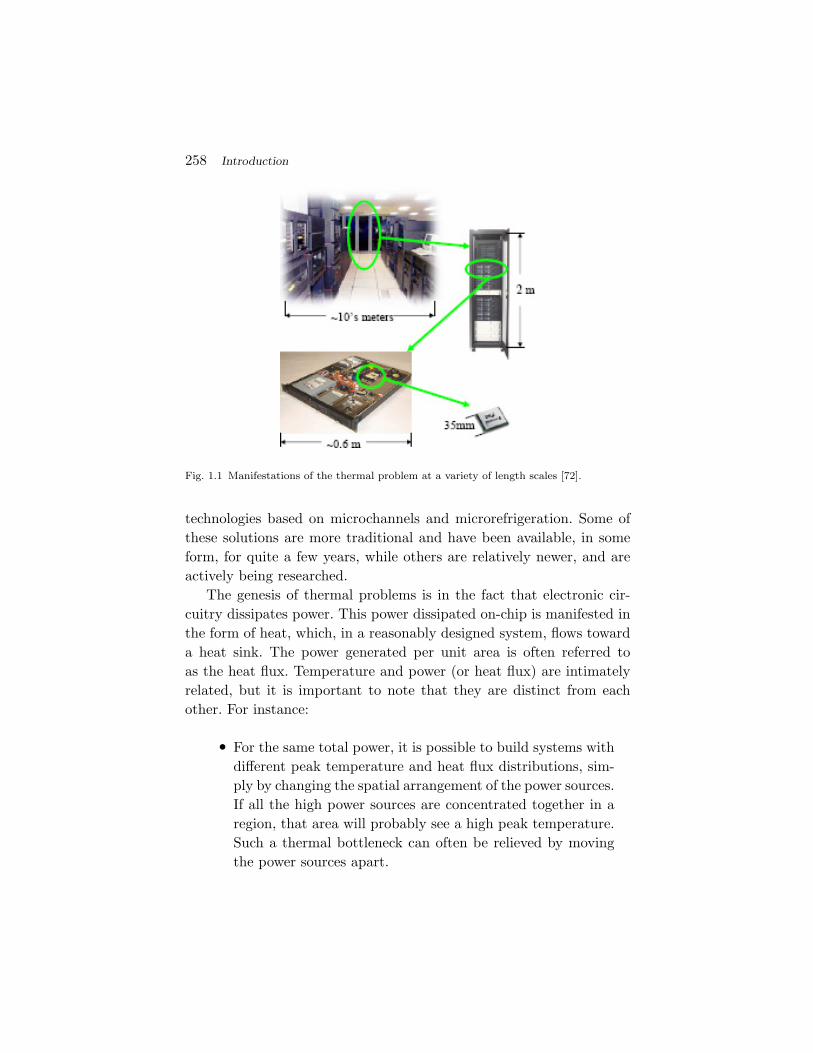
Thermal analysis is important in ensuring the accuracy of timing,noise, and reliability analyses during chip design. The thermal prop-erties of integrated systems can be studied at a number of levels andlength scales, as partly illustrated in Figure 1.1. For the problemof cooling racks of computing servers in a data center, the coolingstructure must cover an area of the order of meter to tens of meters.At the next level, board-level cooling operates at length scales of theorder of a tenth of a meter, while package level cooling correspondsto lengths of the order of centimeters. Within-chip solutions includemicrorefrigeration solutions, whose sizes range from the order of amillimeter to a centimeter [130] and can operate at the architecturallevel, to solutions that can scale down to several tens of microns [129]and operate at about the logic level.
In other words, the thermal problem is important at a wide rangeof length scales, and known cooling solutions exist at all of these levels.These solutions range in complexity and cost from the use of pas-sive heat sinks, to active convective cooling using fans, to more exotic
257
258 Introduction
Fig. 1.1 Manifestations of the thermal problem at a variety of length scales [72].
technologies based on microchannels and microrefrigeration. Some ofthese solutions are more traditional and have been available, in someform, for quite a few years, while others are relatively newer, and areactively being researched.
The genesis of thermal problems is in the fact that electronic cir-cuitry dissipates power. This power dissipated on-chip is manifested inthe form of heat, which, in a reasonably designed system, flows towarda heat sink. The power generated per unit area is often referred toas the heat flux. Temperature and power (or heat flux) are intimatelyrelated, but it is important to note that they are distinct from eachother. For instance:
• For the same total power, it is possible to build systems withdifferent peak temperature and heat flux distributions, sim-ply by changing the spatial arrangement of the power sources.If all the high power sources are concentrated together in aregion, that area will probably see a high peak temperature.Such a thermal bottleneck can often be relieved by movingthe power sources apart.
1.1 Overview 259
• The relative location of the power sources to the heatsink also plays a part in determining the on-chip temper-ature, and by providing high-power elements with a conduc-tive path to the heat sink, many thermal problems can bealleviated.
Most such optimizations can result in tradeoffs: for instance, thermalconsiderations imply that highly active units should be moved apart,but if these units communicate with each other, performance require-ments may dictate that they be kept close to each other.
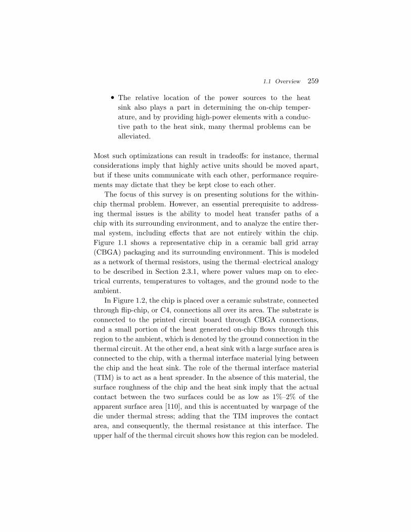
The focus of this survey is on presenting solutions for the within-chip thermal problem. However, an essential prerequisite to address-ing thermal issues is the ability to model heat transfer paths of achip with its surrounding environment, and to analyze the entire ther-mal system, including effects that are not entirely within the chip.Figure 1.1 shows a representative chip in a ceramic ball grid array(CBGA) packaging and its surrounding environment. This is modeledas a network of thermal resistors, using the thermal–electrical analogyto be described in Section 2.3.1, where power values map on to elec-trical currents, temperatures to voltages, and the ground node to theambient.
In Figure 1.2, the chip is placed over a ceramic substrate, connectedthrough flip-chip, or C4, connections all over its area. The substrate isconnected to the printed circuit board through CBGA connections,and a small portion of the heat generated on-chip flows through thisregion to the ambient, which is denoted by the ground connection in thethermal circuit. At the other end, a heat sink with a large surface area isconnected to the chip, with a thermal interface material lying betweenthe chip and the heat sink. The role of the thermal interface material(TIM) is to act as a heat spreader. In the absence of this material, thesurface roughness of the chip and the heat sink imply that the actualcontact between the two surfaces could be as low as 1%–2% of theapparent surface area [110], and this is accentuated by warpage of thedie under thermal stress; adding that the TIM improves the contactarea, and consequently, the thermal resistance at this interface. Theupper half of the thermal circuit shows how this region can be modeled.

260 Introduction
Fig. 1.2 Heat dissipation paths of a chip in a system.
Additional air-cooling schemes, such as fans that are connected to theheat sink, can be incorporated into this model.
A crucial step in design involves the choice of a heat sink: here,approximate techniques may be used to obtain a reasonable sinkingsolution [88], based on a gross characterization of the sink by its thermalresistance. At the package design level, a key item of interest is thethermal design power (TDP), which is the maximum sustained powerdissipated by an integrated circuit. This is not necessarily the peakpower: if the peak power is dissipated for a small period of time thatis below the thermal time constant, it does not appreciably affect thechoice of the heat sink. If the peak temperature is to be maintained at atemperature Tpeak above the ambient temperature, then the maximumthermal resistance of the heat sink is given by a simple formula basedon a lumped DC analysis:
Rsink = Tpeak/TDP. (1.1)
The choice of the heat sink can be made on the basis of this requirement.Note that this is a very coarse analysis that does not consider transienteffects.
1.2 Thermal Trends 261
1.2 Thermal Trends
1.2.1 The Importance of Temperature as a DesignConsideration
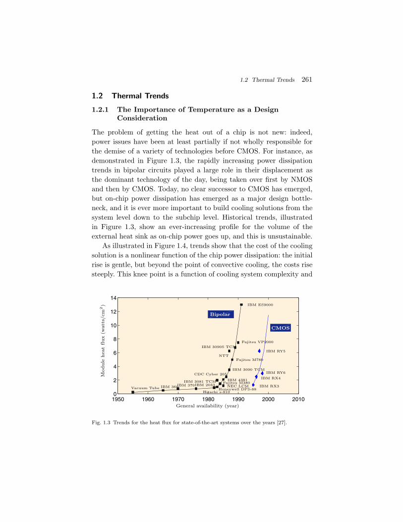
The problem of getting the heat out of a chip is not new: indeed,power issues have been at least partially if not wholly responsible forthe demise of a variety of technologies before CMOS. For instance, asdemonstrated in Figure 1.3, the rapidly increasing power dissipationtrends in bipolar circuits played a large role in their displacement asthe dominant technology of the day, being taken over first by NMOSand then by CMOS. Today, no clear successor to CMOS has emerged,but on-chip power dissipation has emerged as a major design bottle-neck, and it is ever more important to build cooling solutions from thesystem level down to the subchip level. Historical trends, illustratedin Figure 1.3, show an ever-increasing profile for the volume of theexternal heat sink as on-chip power goes up, and this is unsustainable.
As illustrated in Figure 1.4, trends show that the cost of the coolingsolution is a nonlinear function of the chip power dissipation: the initialrise is gentle, but beyond the point of convective cooling, the costs risesteeply. This knee point is a function of cooling system complexity and
1950 1960 1970 1980 1990 2000 20100
2
4
6
8
10
12
14
Fig. 1.3 Trends for the heat flux for state-of-the-art systems over the years [27].

262 Introduction
20 30 40 50 60 70 800
10
20
30
40
Fig. 1.4 Cooling costs as a function of the power dissipation [57].
the volume of actively cooled packages/technologies, and may arguablypermit slightly higher on-chip power dissipation in the future as newertechnologies gain economies of scale, but the fundamental nature of thecurve — of having a gentle ascent followed by a steep rise beyond aknee point — is unlikely to change. This has consequences on the sizeof the heat sink, and Figure 1.5 shows how the volume of the heat sinkhas increased with increased on-chip power.
To achieve the required heat sinking solution, it may be necessaryto increase the heat sink size to unreasonable levels, or to move to newcooling technologies. For contemporary high-end, large-volume parts,anything that is more complex than air-cooling is probably too expen-sive. Although several of the bipolar chips in Figure 1.3, after 1980,used some form of water cooling [27], liquid cooling is not seen as avery viable solution today. There have been numerous improvementseven in air-cooled technologies and improved thermal interface mate-rials in the recent past, which have progressively shifted the knee ofthe cooling cost curve of Figure 1.4 progressively to the right, so thatthe heat fluxes that are currently obtained by air cooling could onlybe achieved by liquid cooling in the 1980s [120]. However, even theseimprovements cannot keep up with the capability of Moore’s law tointegrate more functionality on a chip. Indeed, while it is possible to

1.2 Thermal Trends 263
0 20 40 60 80
50
100
150
200
250
300
350
Fig. 1.5 Historical data showing the volume of the heat sink as a function of the totalon-chip power [72].
pack more transistors on a chip today, only a fraction of them canactually be used to full potential, because of power and thermal limita-tions. More advanced solutions using, for example microfluidic channelsand microrefrigeration, have been proposed, these are not cost-effectiveenough for widespread use today.
1.2.2 Thermal Issues in 3D Integrated Circuits
The previous subsection explains why temperature must be an impor-tant consideration in the design of nanoscale integrated circuits. A fur-ther motivator for thermally conscious design has come about with theadvent of three dimensional (3D) integration, which makes the on-chipproblem particularly acute.
Unlike conventional 2D circuits, where all transistors are placed in asingle plane, with several layers of interconnect above, 3D circuits stacktiers of such 2D structures, one above the other. 3D structures may bebuilt by stacking tiers of dies above each other, where the separationbetween tiers equals the thickness of the bulk substrate, which is of

264 Introduction
Fig. 1.6 A schematic of a 3D integrated circuit.
the order of several hundreds of microns. Advances in industrial [54],government [18], and academic [117] research laboratories have demon-strated 3D designs with inter-tier separations of the order of a fewmicrons, enabling short connections between tiers, accentuating theadvantages of short vertical interconnections in these 3D structures.A schematic of a 3D chip is illustrated in Figure 1.6, showing five tiersstacked over each other. The lowest tier sits over a bulk substrate,while the other tiers are thinned to remove the substrate, and provideinter-tier distances of the order of ten microns.
With these technological advances, 3D technologies provide aroadmap for allowing increased levels of integration within the samefootprint, in a direction that is orthogonal to Moore’s law. Moreover,3D technologies provide the ability to locate critical blocks close to eachother, e.g., by placing memory units in close proximity to processors byplacing them one above the other. These, and other, advantages make3D a promising technology for the near future.
However, the increased packing density afforded by 3D integrationhas the drawback of exacerbating thermal issues. Based on a simpleback-of-the-envelope calculation, a k-tier 3D chip could use k times asmuch current as a single 2D chip of the same footprint; however, the

1.3 Organization of the Survey 265
packaging technology is not appreciably different. This implies thatthe corresponding heat generated must be sent out to the environ-ment using a package with essentially similar heat sinking capabilities.As a result, the on-chip temperature on a 3D chip could be k timeshigher than the 2D chip. While this is a very coarse analysis with verycoarse assumptions, the eventual conclusion — that thermal effects area major concern in 3D circuits — is certainly a strong motivator forpaying increased attention to thermal issues today.
1.3 Organization of the Survey
This survey begins its discussion of on-chip thermal effects by survey-ing techniques for evaluating the distribution of temperature on a chip.These analysis techniques essentially solve a partial differential equa-tion (PDE) that relates the power dissipated on a chip to its tempera-ture profile. While the solution of PDEs is a well-studied problem, it ispossible to take advantage of some specific properties of the on-chipproblem to obtain an efficient solution. Moreover, thermal analysisshows similarities to other well-studied problems in integrated circuitdesign, most notably, those of analyzing on-chip power grids [126], andof substrate analysis [46, 36], and techniques from these domains canbe borrowed to enhance the quality of algorithms for thermal analysis.
Next, we study the manner in which on-chip temperatures affectthe properties and performance of a circuit. In terms of delay, the per-formance of transistors and the resistance of interconnect wires can beaffected; in terms of power dissipation, there is a strong relationship,with potential feedback, between temperature and leakage power; interms of reliability, the lifetime of both devices and interconnects alldepend critically on the operating temperature of the circuit. These areall critical factors in ensuring circuit performance, and the complexityof these problems makes it essential to build efficient and scalable CADsolutions for on-chip thermal analysis. Finally, we overview some rep-resentative techniques for thermally driven circuit optimization.
2Thermal Analysis Algorithms
2.1 Overview
A basic requirement for addressing on-chip thermal issues is to developthe ability to analyze and predict the thermal behavior of an inte-grated circuit. Several algorithms for on-chip thermal analysis havebeen presented in the literature, for application areas ranging fromarchitecture level analysis to cell level analysis to transistor-level anal-ysis. This section overviews these methods and provides the back-ground required to understand techniques for formulating and solvingthe thermal PDE.
The foundations of thermal analysis lie in classical heat transfertheory, which has been well-studied over the years. However, there areseveral features that are specific to the on-chip context that a thermalanalyzer may take advantage of. For example:
• On-chip geometries are strongly rectilinear in nature: forexample, all wires are routed in the coordinate directionsin mainstream technologies; standard cells are generally rec-tilinear in outline, as are many functional blocks on a chip.Therefore, it is reasonable to assume, at above the device
266
2.1 Overview 267
level, that the topologies that we will deal with are rectilin-ear. This implies the existence of a certain set of rectangulargeometric symmetries that may be leveraged.
• The devices, which are the major heat-producing elements,lie in either a single layer (in classical 2D technologies), or inmultiple layers (in 3D technologies) atop a substrate, and thepoints at which a user is typically interested in analyzing tem-perature are within the device layer(s). This implies that thesubstrate, which is much more voluminous than the devicelayer, can be abstracted away into a macromodel. This isparticularly useful when repeated evaluations are necessary,corresponding to, for example, different placements withinthe same die area.
• Due to the top-down nature of the IC design process, the levelof accuracy of the power estimates vary at different steps inthe design cycle. Correspondingly, the accuracy requirementsare also variable. Generally speaking, early steps of the designcycle can be very influential in impacting the overall perfor-mance of the design: in fact, the most effective optimiza-tions can be made at these stages, but they must necessarilyoperate under limited information. A coarser analysis isappropriate at this stage. At later steps in the design cycle, asmore of the design becomes concrete, the information that isavailable is more detailed, but the flexibility to make changesis limited. The role of detailed thermal analysis at this stageis to ensure that the assumptions made in early stages ofdesign are maintained (or improved upon), so that high-leveloptimizations made under these assumptions can be effective.
This survey presents an overview of techniques for full-chip thermalanalysis. Another important problem, that of Joule heating in wires, isnot covered here, but the reader is referred to, for example, [3, 4, 26]for further guidance on this topic. We begin with an explanation of theunderlying PDEs that describe the thermal system. Next, we describetechniques for solving these PDEs in the steady-state, followed by adescription of techniques for solving the linear equations that arise

268 Thermal Analysis Algorithms
from discretizing the PDEs. Finally, we describe techniques for solvingthe transient analysis problem.
2.2 The Thermal PDE
2.2.1 Overview
The problem of on-chip thermal analysis requires the solution of theheat equation, which is described in terms of a PDE. Most commonly,PDEs are solved using a discretization or meshing scheme, which con-verts the problem to one of solving a set of algebraic equations that aretypically linear. Several approaches and algorithms for thermal analysishave been published in the literature. Depending on the context, thestage of design, and the degree of accuracy that is necessary, differentclasses of algorithms may be appropriate. Various choices are possiblealong the way, in the PDE that is used to describe the thermal analysisproblem, in the solution framework and discretization scheme for thenumerical solution of the PDE, and in the solution technique for theresulting equations after discretization. In many cases, our methods willfocus on uniform discretization for simplicity, but it is understood thatthere is a need for nonuniform discretization, to obtain more accuratesolutions to temperature-sensitive parts of a chip.
The precise PDE that is used to model the thermal problem dependson the length scale being considered. For full-chip thermal analysis,the analysis is necessarily performed at a coarse-grained level, andmacroscale analysis based on the Fourier equation is adequate. How-ever, if the analysis is to be performed at small length scales, thena more detailed solution that takes quantum-mechanical effects intoaccount is required. Another choice is related to determining whetherthe thermal problem is to be solved for the steady-state or the tran-sient case. The former assumes that the temperature waveforms aresteady over time, so that expressions related to time-derivatives can beignored, while the latter presents the temporal response to (possibly)time-varying input stimuli. In other words, transient analysis solves thefull PDE, considering both the space variable r and the time variablet as independent variables, unlike steady-state analysis, which sets allpartial derivatives with respect to t in the full PDE to zero and thus

2.2 The Thermal PDE 269
entirely removes the time variable t from the equation. To the readerschooled in circuit analysis, these ideas will seem familiar, since theyparallel the notion of steady-state and transient simulation in circuitanalysis.
This survey is primarily directed toward solving full-chip thermalanalysis problems, which implies that the underlying PDE is the heatequation, as derived from Fourier’s law (although we provide a briefreview of the transistor-level analysis problem). To solve this prob-lem numerically, one of several frameworks for PDE solution may beemployed, such as the finite difference method (FDM), the finite ele-ment method (FEM), and the Green function method. In case of theFDM and FEM, a set of linear equations is generated, which must besolved to determine the temperature distribution within the system.Depending on the properties of the linear equations, they can be solvedby, for example, a direct method based on LU/Cholesky factorization,or an iterative method such as ICCG and GMRES, or a random walkbased method, as described in Section 2.4.
2.2.2 Macroscale Fourier-based Analysis
Conventional heat transfer in a chip is described by Fourier’s law ofconduction [103], which states that the heat flux, q (in W/m2), is pro-portional to the negative gradient of the temperature, T (in K), withthe constant of proportionality corresponding to the thermal conduc-tivity of the material, kt (in W/(m K)), i.e.,
q = −kt∇T. (2.1)
The divergence of q in a region is the difference between the powergenerated and the time rate of change of heat energy in the region. Inother words,
∇ · q = −kt∇ · ∇T = −kt∇2T = g(r, t) − ρcp∂T (r, t)
∂t. (2.2)
Here, r is the spatial coordinate of the point at which the temperatureis being determined, t represents time (in sec), g is the power densityper unit volume (in W/m3), cp is the heat capacity of the chip material

270 Thermal Analysis Algorithms
(in J/(kg K)), and ρ is the density of the material (in kg/m3). This maybe rewritten as the following heat equation, which is a parabolic PDE:
ρcp∂T (r, t)
∂t= kt∇2T (r, t) + g(r, t). (2.3)
The thermal conductivity, kt, in a uniform medium is isotropic, andthermal conductivity values for silicon, silicon dioxide, and metals suchas aluminum and copper are fundamental material properties whosevalues can be determined from standard tables. In practice, in earlystages of analysis and for optimization purposes, integrated circuitsmay be assumed to be layer-wise uniform in terms of thermal con-ductivity. The bulk layer has the conductivity of bulk silicon, and theconductivity of the metal layers is often computed using an averagingapproach: this region consists of a mix of silicon dioxide and metal, anddepending on the metal density within the region, an effective thermalconductivity may be used for macroscale analysis. The value of kt isweakly dependent on temperature, which makes the heat equation non-linear. However, for on-chip analysis, this nonlinearity is often ignored,although approaches to solving thermal problems under nonlinear ther-mal conductivities [11] have been proposed. In many applications, theprecise worst-case power patterns have some uncertainty associatedwith them, so that such approximations are acceptable.
The solution to Equation (2.3) corresponds to the transient thermalresponse. In the steady state, all derivatives with respect to time go tozero, and therefore, steady-state analysis corresponds to solving thePDE:
∇2T (r) = −g(r)kt
. (2.4)
This is the well-known Poisson’s equation.The time constants of heat transfer are of the order of millisec-
onds, and are much longer than the subnanosecond clock periods intoday’s VLSI circuits. Therefore, if a circuit remains within the samepower mode for an extended period of time, and its power density dis-tribution remains relatively constant, steady-state analysis can capturethe thermal behavior of the circuit accurately. Even if this is not thecase, steady-state analysis can be particularly useful for early and more

2.2 The Thermal PDE 271
approximate analysis, in the same spirit that steady-state analysis isused to analyze power grid networks early in the design cycle. On theother hand, when greater levels of detail about the inputs are available,or when a circuit makes a number of changes between power modes attime intervals above the thermal time constant, transient analysis ispossible and potentially useful.
To obtain a well-defined solution to Equation (2.3), a set of bound-ary conditions must be imposed. The most generally used boundaryconditions in thermal analysis for chip design are described in Dirichletform, specifying information on the boundary, Γ, of the region. In thesucceeding discussion, we will use Tc to denote a constant temperature,n for the outward normal direction of the boundary surface, h is theeffective heat transfer coefficient of the ambient, and Ta is the tem-perature of the ambient. Examples of typical boundary conditions forthe on-chip thermal analysis problem are listed below (for details, thereader is referred to a standard text on heat transfer, such as [103]):
• The isothermal boundary condition can be applied when asurface of the chip is attached to a constant temperatureheat reservoir with a significantly larger heat capacity andhigher thermal conductivity than those of the chip itself, andis specified as:
T (r, t) = Tc where r ∈ Γ. (2.5)
This boundary condition is sometimes used to model theeffect of the heat spreader and heat sink in the chip-packagestack shown in Figure 2.1. However, the assumption of con-stant temperature at the boundary that is made here is anapproximation in real designs that is not appropriate whenhigher accuracies are necessary.
• The heat flux boundary condition can be applied when powersources are placed on a surface of the chip. For example, ifthe heat transfer within interconnect layers is ignored, thepower generating devices can be modeled using the followingheat flux boundary conditions as far as the silicon substrate

272 Thermal Analysis Algorithms
Heat spreaderHeat sink
Chip
Fig. 2.1 Schematic of an IC chip with the associated packaging.
is concerned:
kt∂T (r, t)
∂n= p(r, t) where r ∈ Γ, (2.6)
where p(r, t) is the heat flux at a boundary point r, as afunction of time. In this case, the heat source is idealized tobe part of the boundary conditions; more realistically, theheat source is part of the material structure being studied.
• A special case of the heat flux boundary condition has provento be rather useful, i.e., the adiabatic boundary condition,which can be obtained by setting the power term to zero inthe heat flux condition. The adiabatic boundary conditioncan be applied when there is no heat exchange across thesurface of the chip, and it is often a good approximationwhen the corresponding surface of the chip is covered by thickoxide, which is a thermal insulator, or for heat exchange onthe sides of a chip.
• The convective boundary condition is often used to model theeffect of the heat spreader and heat sink in thermal analysis,and can be written as:
−kt∂T (r, t)
∂n= hc(T (r, t) − Ta) where r ∈ Γ. (2.7)
This condition states that the heat flow to the surface fromthe chip side equals the heat dissipated to the ambient bythe heat sink and the surrounding air. It is worth noticing
2.2 The Thermal PDE 273
that the effective heat transfer coefficient hc used in thermalanalysis for chip design is a property of the heat sink, and isusually much larger than that of the air, due to the fact thatthe heat sink has significantly increased the effective heatdissipation area of the chip.
When a more detailed package model is available, it may beappended into the overall thermal analysis approach. For example,Hotspot [60, 61, 62, 63, 64, 135, 134] demonstrates how a package modelcan be inserted into a coarse FDM solver; the boundary conditions forthe package are taken to be isothermal.
2.2.3 Nanoscale Thermal Analysis
The condition under which Equation (2.3) can be applied is in theFourier regime, where it is reasonable to assume that local thermo-dynamic equilibrium can be maintained. Here, “local thermodynamicequilibrium” refers to the case where the properties of the system suchas the distribution of energy-carrying particles as a function of locationr and velocity v may change with space and time, but they change soslowly that any macroscopically small but microscopically large regionwithin the system can be well approximated by an equilibrium state atany time. For systems violating such conditions, quantum-mechanicaleffects must be taken into account. The material in this section drawsstrongly from [109], which is commended to the reader for furtherdetails. Since the focus of this survey is on macroscale thermal effects,only a brief overview is provided in this section, for completeness.
The local thermodynamic equilibrium assumption is valid forcoarse-grained, system-level or full-chip thermal analysis, but forfine-grained analysis of systems with aggressively scaled devices undervery strong electric fields, the systems may show nonequilibrium prop-erties, so that the application of Equation (2.3) can underestimate theeffective temperatures of the hot spots [121]. At these microscales, itis necessary to consider the effects of electron–phonon interactions.Phonons essentially correspond to energy due to lattice vibrations in acrystal, and their effects are quantum-mechanical. As device dimensionsbecome comparable to the mean free path of electrons and phonons
274 Thermal Analysis Algorithms
(whose values are, respectively, about 5–10 nm and 200–300 nm for bulksilicon at 300 K [109]), it is necessary to consider their effects on fine-grained thermal analysis.
This mechanism can be summarized as follows: the applied electricfield causes electrons to accelerate as they reach the drain of a transis-tor, causing them to gain energy and heat up. This can lead to electronpopulation to lose energy due to scattering with lattice vibrations (i.e.,phonons), which results in Joule heating as the lattice is heated up andgains temperature. The phonons further affect the electron mobility:in essence, the electrons and phonons affect behavior of each other.Low energy electrons scatter with lower-frequency acoustic phonons,while higher energy electrons scatter with the higher-frequency opticalphonons. Acoustic phonons move faster through silicon, they dominateheat transfer in silicon in tenths of picoseconds, while optical phononsdegrade over longer periods of time (of the order of picoseconds) toacoustic modes, which can cause temperature rises.
At the fine-grained level within a transistor, power dissipation inCMOS transistors occurs in tens of picoseconds, during a switchingevent, but Fourier conduction modes have time constants of the orderof tens of nanoseconds across the length of a gate. This implies that dueto the electron–phonon interactions, the local thermodynamic equilib-rium assumption does not hold at these length scales. Temperature isa statistical quantity that depends on an equilibrium state, and theselength and time scales disallow a continuum assumption for heat trans-fer. Instead, the distribution of phonons can be used to determine an“effective temperature” by equating the nonequilibrium energy densityto that from Bose–Einstein statistics.
To determine phonon distributions, one can solve the Boltzmanntransport equation
∂Nq(r, t)∂t
+ vg·∇rNq(r, t) + F·∇�qNq(r, t)
=∂Nq(r, t)
∂t
∣∣∣collision
+∂Nq(r, t)
∂t
∣∣∣generation
. (2.8)
This has to be used to study the movement of energy-carrying parti-cles and the phenomenon of heat transfer. Here, Nq(r, t) is the number
2.3 Steady-state Thermal Analysis Algorithms 275
of particles in a particular mode with wave vector q at position r andtime t, vg is the group velocity of that mode, and F is an external forceacting on the particle. The two terms on the right-hand side of the equa-tion correspond to changes in the number of particles in that mode dueto collisions and the generation of particles. The Boltzmann transportEquation (2.8) is valid for the semi-classical transport regime wherecharge and energy carriers can be treated as particles between scatter-ing events but the frequency and nature of the scattering is describedusing quantum mechanics. Because the collision and generation termsare not known a priori, the solution of the Boltzmann transport equa-tion often involves some Monte Carlo type of simulations of the actualinteractions between individual particles.
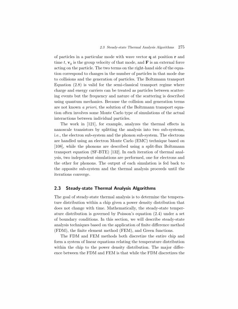
The work in [121], for example, analyzes the thermal effects innanoscale transistors by splitting the analysis into two sub-systems,i.e., the electron sub-system and the phonon sub-system. The electronsare handled using an electron Monte Carlo (EMC) technique based on[108], while the phonons are described using a split-flux Boltzmanntransport equation (SF-BTE) [132]. In each iteration of thermal anal-ysis, two independent simulations are performed, one for electrons andthe other for phonons. The output of each simulation is fed back tothe opposite sub-system and the thermal analysis proceeds until theiterations converge.
2.3 Steady-state Thermal Analysis Algorithms
The goal of steady-state thermal analysis is to determine the tempera-ture distribution within a chip given a power density distribution thatdoes not change with time. Mathematically, the steady-state temper-ature distribution is governed by Poisson’s equation (2.4) under a setof boundary conditions. In this section, we will describe steady-stateanalysis techniques based on the application of finite difference method(FDM), the finite element method (FEM), and Green functions.
The FDM and FEM methods both discretize the entire chip andform a system of linear equations relating the temperature distributionwithin the chip to the power density distribution. The major differ-ence between the FDM and FEM is that while the FDM discretizes the
276 Thermal Analysis Algorithms
differential operator, the FEM discretizes the temperature field. Theprimary advantage of the FDM and FEM is their capability of han-dling complicated material structures, particularly nonuniform inter-connect distributions in a VLSI chip. However, a direct applicationof the FDM or the FEM may be computationally wasteful since itmay discretize the entire volume of the chip. Such an approach failsto recognize that the regions on a chip where power is generated, orwhose temperature is of interest, are usually located only on a fewdiscrete planes, e.g., the device layer and interconnect layers. In otherwords, a direct application of these methods will result in intimidat-ingly large systems of algebraic equations, which can take a large num-ber of CPU cycles to solve, leading to relatively low efficiencies inthermal analysis. Using macromodeling techniques, it is possible toabstract away [139] the nodes in the FDM and FEM meshes that theusers of the thermal simulator are not interested in, although it shouldbe noted that this macromodeling procedure can be computationallyintensive.
In contrast with these methods, the Green function method pro-vides a semi-analytical solution in which only the layers where thepower is generated or whose temperature is of interest are analyzed.Therefore, the resulting problem size is usually small compared withthat of the FDM and FEM, which reduces the time that is needed toreach a solution to the problem. However, this improvement comes at acost: the application of the Green function method is usually based onthe assumption that the chip materials are layer-wise uniform, whichis often not satisfied especially for interconnect layers. As a result, theGreen function method is more suitable for early stages of physicaldesign, where the accuracy requirement on thermal analysis is moder-ate but the efficiency requirement is high. The computational efficiencyis driven by the fact that no algebraic equations have to be solved inthe Green function method after the Green function has been deter-mined. Therefore, a significant portion of research works related to theapplication of the Green function method in thermal analysis for chipdesign have been directed toward the fast evaluations of the Greenfunction.
2.3 Steady-state Thermal Analysis Algorithms 277
2.3.1 The Finite Difference Method
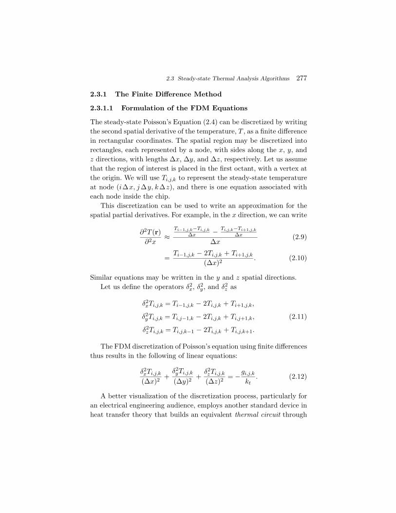
2.3.1.1 Formulation of the FDM Equations
The steady-state Poisson’s Equation (2.4) can be discretized by writingthe second spatial derivative of the temperature, T , as a finite differencein rectangular coordinates. The spatial region may be discretized intorectangles, each represented by a node, with sides along the x, y, andz directions, with lengths ∆x, ∆y, and ∆z, respectively. Let us assumethat the region of interest is placed in the first octant, with a vertex atthe origin. We will use Ti,j,k to represent the steady-state temperatureat node (i∆x, j ∆y, k∆z), and there is one equation associated witheach node inside the chip.
This discretization can be used to write an approximation for thespatial partial derivatives. For example, in the x direction, we can write
∂2T (r)∂2x
≈Ti−1,j,k−Ti,j,k
∆x − Ti,j,k−Ti+1,j,k
∆x
∆x(2.9)
=Ti−1,j,k − 2Ti,j,k + Ti+1,j,k
(∆x)2. (2.10)
Similar equations may be written in the y and z spatial directions.Let us define the operators δ2
x, δ2y , and δ2
z as
δ2xTi,j,k = Ti−1,j,k − 2Ti,j,k + Ti+1,j,k,
δ2yTi,j,k = Ti,j−1,k − 2Ti,j,k + Ti,j+1,k, (2.11)
δ2zTi,j,k = Ti,j,k−1 − 2Ti,j,k + Ti,j,k+1.
The FDM discretization of Poisson’s equation using finite differencesthus results in the following of linear equations:
δ2xTi,j,k
(∆x)2+
δ2yTi,j,k
(∆y)2+
δ2zTi,j,k
(∆z)2= −gi,j,k
kt. (2.12)
A better visualization of the discretization process, particularly foran electrical engineering audience, employs another standard device inheat transfer theory that builds an equivalent thermal circuit through

278 Thermal Analysis Algorithms
the so-called thermal–electrical analogy. Each node in the discretiza-tion corresponds to a node in the circuit. The steady-state equationcorresponds to a network where “thermal resistors” are connectedbetween nodes that correspond to spatially adjacent regions, and “ther-mal current sources” that map on to power sources. The voltages atthe nodes in this thermal circuit can then be computed by solvingthe circuit, and these yield the temperature at that node. Mathemati-cally, this can be derived from Equation (2.4) by writing the discretizedequation in a slightly different form from Equation (2.12). For exam-ple, in the x direction, the finite difference in Equation (2.9) can berewritten as
∂2T (r)∂2x
≈[Ti−1,j,k − Ti,j,k
Ri−1,j,k− Ti,j,k − Ti+1,j,k
Ri,j,k
]· 1ktAx∆x
, (2.13)
where Ri−1,j,k = ∆xktAx
and Ax = ∆y∆z is the cross-sectional area ofthe element when sliced along the x-axis, to obtain the followingdiscretization:[
Ti−1,j,k − Ti,j,k
Ri−1,j,k+
Ti+1,j,k − Ti,j,k
Ri,j,k
]
+[Ti,j−1,k − Ti,j,k
Ri,j−1,k+
Ti,j+1,k − Ti,j,k
Ri,j,k
]
+[Ti,j,k−1 − Ti,j,k
Ri,j,k−1+
Ti,j,k+1 − Ti,j,k
Ri,j,k
]= −Gi,j,k, (2.14)
where Gi,j,k = gi,j,k∆V is the total power generated within the element,and ∆V = Ax∆x = Ay∆y = Az∆z.
The representation (2.14) can readily be recognized as being equiv-alent to the nodal equations at each node of an electrical circuit,where the node is connected to the nodes corresponding to its sixadjacent elements through thermal resistors, as shown in Figure 2.2.In other words, the solution to the thermal analysis problem usingFDM amounts to the solution of a circuit of linear resistors and currentsources.
The ground node, or reference, for the circuit corresponds to a con-stant temperature node, which is typically the ambient temperature.
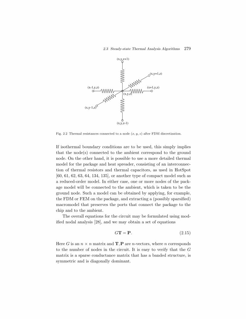
2.3 Steady-state Thermal Analysis Algorithms 279
(x,y-1,z)
(x-1,y,z) (x+1,y,z)
(x,y,z)
(x,y,z-1)
(x,y,z+1)
(x,y+1,z)
Fig. 2.2 Thermal resistances connected to a node (x, y, z) after FDM discretization.
If isothermal boundary conditions are to be used, this simply impliesthat the node(s) connected to the ambient correspond to the groundnode. On the other hand, it is possible to use a more detailed thermalmodel for the package and heat spreader, consisting of an interconnec-tion of thermal resistors and thermal capacitors, as used in HotSpot[60, 61, 62, 63, 64, 134, 135], or another type of compact model such asa reduced-order model. In either case, one or more nodes of the pack-age model will be connected to the ambient, which is taken to be theground node. Such a model can be obtained by applying, for example,the FDM or FEM on the package, and extracting a (possibly sparsified)macromodel that preserves the ports that connect the package to thechip and to the ambient.
The overall equations for the circuit may be formulated using mod-ified nodal analysis [28], and we may obtain a set of equations
GT = P. (2.15)
Here G is an n × n matrix and T,P are n-vectors, where n correspondsto the number of nodes in the circuit. It is easy to verify that the G
matrix is a sparse conductance matrix that has a banded structure, issymmetric and is diagonally dominant.

280 Thermal Analysis Algorithms
2.3.1.2 Building a Compact Model for the Substrate
The finite difference approach was utilized for on-chip thermal analysisin [139], which also realized that a large number of nodes in the tem-perature vector can be eliminated. Specifically, these nodes in the finitedifference discretization can be classified into two categories: those onthe surface of the region, in the region where the active devices lie, andthose within the substrate, which we will call the internal nodes. Inmost cases, the temperatures at internal nodes are not of interest, andthe power density at these nodes is zero. Therefore, the correspondingvariables can be eliminated to build a compact model for the thermalsystem.
Under this classification, Equation (2.15) can be rewritten, by par-titioning G into submatrices, as[
GP GTC
GC GI
][T
TI
]=[P
0
], (2.16)
where TI is the vector of temperatures at the internal nodes, and T
corresponds to the temperatures at the remaining nodes. Note thatthe right-hand side vector shows zero power at the internal nodes. Thematrix G is appropriately partitioned according to the classification.
Eliminating the temperatures at the internal nodes from Equa-tion (2.16), we have
G′T = P,
where G′ = GP − GTCG−1
I GC
. (2.17)
If the total number of nodes in n, and n − m of these are inter-nal nodes, then the computational cost for directly calculating G′ byinverting GI is O(n3) for a general matrix, if n � m, which is not triv-ial. As an example, for a mesh with a 40 × 40 grid (i.e., m = 1600) inthe x–y direction, and 6 grids in the z direction, we have n = 8000.
The work in [23] generates the matrix G by the column, observingthat the ith column of G is given by Gei, where ei is a m × 1 vectorthat is zero in all positions except the ith position, which is 1. FromEquation (2.17), we have
Gei = GPei − GTCG−1
I GCei. (2.18)
2.3 Steady-state Thermal Analysis Algorithms 281
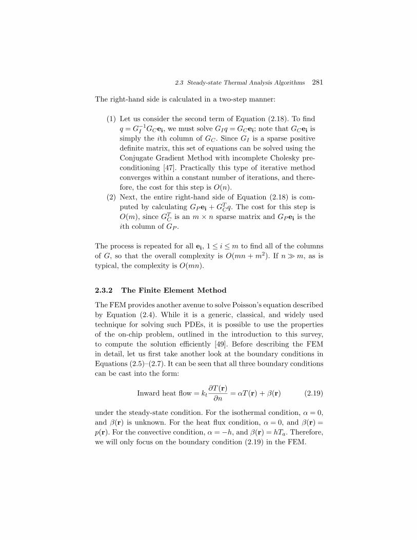
The right-hand side is calculated in a two-step manner:
(1) Let us consider the second term of Equation (2.18). To findq = G−1
I GCei, we must solve GIq = GCei; note that GCei issimply the ith column of GC . Since GI is a sparse positivedefinite matrix, this set of equations can be solved using theConjugate Gradient Method with incomplete Cholesky pre-conditioning [47]. Practically this type of iterative methodconverges within a constant number of iterations, and there-fore, the cost for this step is O(n).
(2) Next, the entire right-hand side of Equation (2.18) is com-puted by calculating GPei + GT
Cq. The cost for this step isO(m), since GT
C is an m × n sparse matrix and GPei is theith column of GP .
The process is repeated for all ei, 1 ≤ i ≤ m to find all of the columnsof G, so that the overall complexity is O(mn + m2). If n � m, as istypical, the complexity is O(mn).
2.3.2 The Finite Element Method
The FEM provides another avenue to solve Poisson’s equation describedby Equation (2.4). While it is a generic, classical, and widely usedtechnique for solving such PDEs, it is possible to use the propertiesof the on-chip problem, outlined in the introduction to this survey,to compute the solution efficiently [49]. Before describing the FEMin detail, let us first take another look at the boundary conditions inEquations (2.5)–(2.7). It can be seen that all three boundary conditionscan be cast into the form:
Inward heat flow = kt∂T (r)
∂n= αT (r) + β(r) (2.19)
under the steady-state condition. For the isothermal condition, α = 0,and β(r) is unknown. For the heat flux condition, α = 0, and β(r) =p(r). For the convective condition, α = −h, and β(r) = hTa. Therefore,we will only focus on the boundary condition (2.19) in the FEM.

282 Thermal Analysis Algorithms
21
34
5 6
78
Fig. 2.3 An 8-node hexahedral element used in the FEM.
A succinct explanation of FEM, as applied to the on-chip case, isprovided in [48]. In finite element analysis, the design space is first dis-cretized or meshed into elements. Different element shapes can be usedsuch as tetrahedra and hexahedra. For the on-chip problem, where allheat sources are modeled as being rectangular, a reasonable discretiza-tion for the FEM [49] divides the chip into 8-node rectangular hexa-hedral elements as shown in Figure 2.3. In the on-chip context, hexa-hedral elements also simplify the book-keeping and data managementduring FEM. The temperatures at the nodes of the elements constitutethe unknowns that are computed during finite element analysis, andthe temperature within an element is calculated using an interpolationfunction that approximates the solution to the heat equation withinthe elements, as shown below:
T (x,y,z) =8∑
i=1
Ni(x,y,z)Ti, (2.20)
where Ni(x,y,z) is the shape function associated with node i and Ti isthe temperature at node i. Let (xc,yc,zc) be the center of the element,and denote the width, depth, and height of the element by w, d, andh, respectively. The temperature at any point within the element isinterpolated in FEM using a shape function, Ni(x,y,z), which in thiscase is written as the trilinear function:
Ni(x,y,z) =(
12
+2(xi − xc)
w2 (x − xc))
×(
12
+2(yi − yc)
d2 (y − yc))
×(
12
+2(zi − zc)
h2 (z − zc))
. (2.21)

2.3 Steady-state Thermal Analysis Algorithms 283
The property of this function is that its value is 1 at vertex i, and zeroat all other vertices, which satisfies the elementary requirement corre-sponding to a vertex temperature, as calculated in Equation (2.20).
From the shape functions, the thermal gradient, g, can be found,using Equation (2.20), as follows:
g =
∂T∂x
∂T∂y
∂T∂z
= BT, (2.22)
where B =
∂N1∂x
∂N2∂x · · · ∂N8
∂x
∂N1∂y
∂N2∂y · · · ∂N8
∂y
∂N1∂z
∂N2∂z · · · ∂N8
∂z
(2.23)
As in the case of circuit simulation using the modified nodal for-mulation [28], stamps are created for each element and added to theglobal system of equations, given by:
KgT = P, (2.24)
where T is the vector of all the nodal temperatures. This system ofequations is typically sparse and can be solved efficiently.
In FEA, these stamps are called element stiffness matrices, K, andtheir values can be determined using techniques based on the calculusof variations. While a complete derivation of this theory is beyond thescope of this survey, and can be found in a standard text on FEM(such as [86]), it suffices to note that the end result yields the followingstamps. For the case where only heat conduction comes into play, wehave
K =∫
VBT DBdV, (2.25)
where V is the volume of the element, and D = diag(kt,x,kt,y,kt,z) is a3 × 3 diagonal matrix in which kt,i, i ∈ {x,y,z} represents the thermalconductivity in each of the three coordinate directions, for the casewhere the region is anisotropic along the three coordinate directions;in many cases, kt,x = kt,y = kt,z = kt.

284 Thermal Analysis Algorithms
For the convective case, if a surface S of the element participatesin convective heat transfer, then the corresponding element stamp isgiven by
K =∫
ShcN
T NdS, (2.26)
where hc is the effective heat transfer coefficient for convection, asdescribed in Equation (2.7). Note that the dimension of K in this casecorresponds to the number of nodes on one surface of the element.
For our hexahedral element, the stamp for the conductive case isgiven by the 8 × 8 symmetric matrix whose entries depend only on w,h, and d, and is given by
K =
A B C D E F G H
B A D C F E H G
C D A B G H E F
D C B A H G F E
E F G H A B C D
F E H G B A D C
G H E F C D A B
H G F E D C B A
, (2.27)
where
A =kt,xhd
9w+
kt,ywd
9h+
kt,zwh
9d
B = −kt,xhd
9w+
kt,ywd
18h+
kt,zwh
18d
C = −kt,xhd
18w− kt,ywd
18h+
kt,zwh
36d
D =kt,xhd
18w− kt,ywd
9h+
kt,zwh
18d
E =kt,xhd
18w+
kt,ywd
18h− kt,zwh
9d
F = −kt,xhd
18w+
kt,ywd
36h− kt,zwh
18d
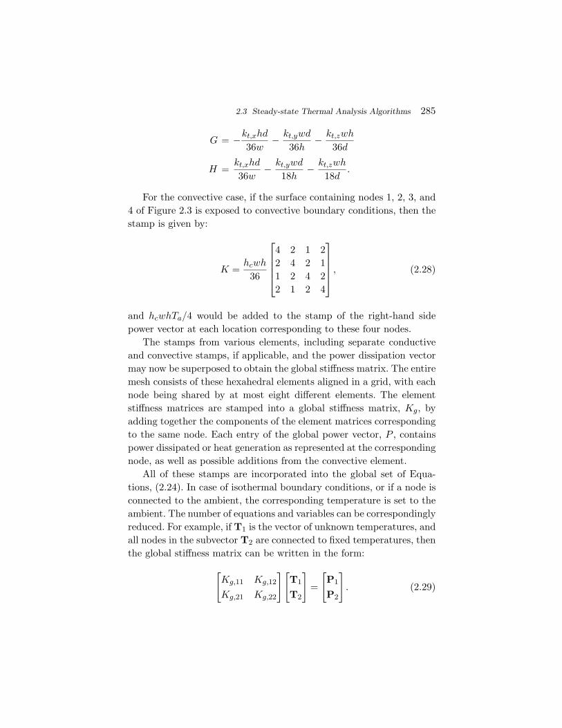
2.3 Steady-state Thermal Analysis Algorithms 285
G = −kt,xhd
36w− kt,ywd
36h− kt,zwh
36d
H =kt,xhd
36w− kt,ywd
18h− kt,zwh
18d.
For the convective case, if the surface containing nodes 1, 2, 3, and4 of Figure 2.3 is exposed to convective boundary conditions, then thestamp is given by:
K =hcwh
36
4 2 1 22 4 2 11 2 4 22 1 2 4
, (2.28)
and hcwhTa/4 would be added to the stamp of the right-hand sidepower vector at each location corresponding to these four nodes.
The stamps from various elements, including separate conductiveand convective stamps, if applicable, and the power dissipation vectormay now be superposed to obtain the global stiffness matrix. The entiremesh consists of these hexahedral elements aligned in a grid, with eachnode being shared by at most eight different elements. The elementstiffness matrices are stamped into a global stiffness matrix, Kg, byadding together the components of the element matrices correspondingto the same node. Each entry of the global power vector, P , containspower dissipated or heat generation as represented at the correspondingnode, as well as possible additions from the convective element.
All of these stamps are incorporated into the global set of Equa-tions, (2.24). In case of isothermal boundary conditions, or if a node isconnected to the ambient, the corresponding temperature is set to theambient. The number of equations and variables can be correspondinglyreduced. For example, if T1 is the vector of unknown temperatures, andall nodes in the subvector T2 are connected to fixed temperatures, thenthe global stiffness matrix can be written in the form:[
Kg,11 Kg,12
Kg,21 Kg,22
][T1
T2
]=
[P1
P2
]. (2.29)

286 Thermal Analysis Algorithms
The fixed values in T2 can be moved to the right-hand side to obtainthe reduced set of equations
Kg,11T1 = P1 − Kg,12T2. (2.30)
2.3.3 Green Function-based Analysis
An alternative to discretization-based methods uses the notion of Greenfunctions to perform steady-state thermal analysis. The Green functionG(r,r′) is defined as the temperature distribution at the point withcoordinate r within the chip, when a unit point power source is placedat location r′. The calculation of the Green function proceeds by solvingPoisson’s equation under a unit impulse excitation at r′, under a similarset of boundary conditions as the original problem, except that theambient temperature, Ta, is taken as the reference. If this functioncan be determined, the temperature distribution within the chip underan arbitrary power density distribution can be calculated, using theprinciple of superposition, as
T (r) = Ta +∫
VG(r,r′)g(r′)dV, (2.31)
where g(r′) is the volume power density distribution, and V is thevolume of the chip.
Green function-based methods have been used for thermal analysisin several works in the literature [70, 148, 149, 150, 166].
We focus here on the work presented in [166]. This begins withthe notion of Green functions, and introduces a number of efficiencyenhancements that exploit the properties of the on-chip thermal analy-sis problem. One such property is that the primary on-chip heat sourcesare the devices, and the points at which the temperature is to be com-puted correspond to locations in the device layer or one of the inter-connect layers. In other words, the points where temperatures mustbe calculated are typically on a set of discrete planes, which will bereferred to as the field planes, and the power sources also lie on a setof discrete planes, which we call the source planes. Therefore, in thedevelopment of Green function-based thermal analysis algorithms, itis often sufficient to focus on a pair of source and field planes (which

2.3 Steady-state Thermal Analysis Algorithms 287
are permitted to be identical to each other). When multiple source andfield planes are present, the temperature distribution can be obtainedeasily through superposition, since the underlying PDE is linear.
The ensuing discussion assumes that the dimension of the chip inthe x and y directions is a and b, respectively. For on-chip applications,it is reasonable to assume that the source and field planes are parallelto each other, and that they correspond to different values of the z
coordinate, say, z and z′, respectively. Given a point (x,y) on the fieldplane, and a point (x′,y′) on the source plane, the Green function canbe written in the following form:
G(x,y,x′,y′) =∞∑
m=0
∞∑n=0
Cmn cos(mπx
a
)cos(nπy
b
)× cos
(mπx′
a
)cos(
nπy′
b
). (2.32)
This formulation assumes that adiabatic boundary conditions areapplied on the sidewalls of the chip. The temperature distribution ata point on the field plane can then be calculated using the followingexpression, in accordance with Equation (2.31):
T (x,y) = Ta +∫
x-rangedx′∫
y-rangedy′G(x,y,x′,y′)p(x′,y′), (2.33)
where p(x′,y′) is the area power density on the source plane.The problem with calculating the temperature distribution on the
field plane directly using Equation (2.33) is that the Green function(2.32) contains infinite summations, and in actual implementations ofthermal analysis algorithms, the summations have to be truncated athigh indices in order to ensure a reasonable accuracy, and this oftenleads to excessively long runtimes.
In [166], the authors developed several high efficiency Greenfunction-based thermal analysis algorithms using ideas similar to thoseproposed by Ghurpurey and Meyer [46] and Costa et al. [36] in the con-text of substrate parasitic extraction, and these algorithms can be usedto perform both localized analysis and full-chip temperature analysis.Three algorithms are presented in the work, and are outlined below:the first algorithm performs localized analysis, the second performs

288 Thermal Analysis Algorithms
full-chip analysis with equal levels of accuracy throughout the chip,and the third performs efficient full-chip analysis for the case wheredifferent regions of the chip may require different levels of accuracy.Each of these operates under simplifying assumptions: that the heatsources are in a plane at the top of the chip, and that the chip haslayerwise uniform thermal conductivities. The first algorithm is suitedfor limited or incremental computations, the second to full-chip analy-sis, and the third to full-chip analysis where the required accuracy indifferent parts is different.
2.3.3.1 Algorithm I: Localized Analysis
For localized analysis, the algorithm proceeds by first establishing afew look-up tables using the Green function coefficients, Cmn, in Equa-tion (2.32). This step can be performed efficiently with the help of thediscrete cosine transform (DCT) [102]. After the look-up tables havebeen established, the calculation of the temperature rise in a rectan-gular shaped field region due to the power generated in a rectangularshaped source region is reduced to a few table look-ups, which is signifi-cantly faster than truncating and evaluating the Green function directlyand then using Equation (2.33) to calculate the temperature rise.
Since on-chip geometries can typically be decomposed into combi-nations of rectangles, we only focus on rectangular-shaped source andfield regions in the following analysis. Figure 2.4 shows a schematic ofa source and a field region. Note that the two regions can have differentz coordinates if the field plane does not coincide with the source plane.
Region
FieldRegion
Source
Fig. 2.4 Source and field regions for computing the temperature distribution.

2.3 Steady-state Thermal Analysis Algorithms 289
Our objective here is to calculate the average temperature Tf of thefield region efficiently given the power density Pd of the source region.To simplify the analysis, it is assumed that Pd is a constant withinthe source region. This is not a very restrictive assumption, since ifthe power density is not uniformly distributed in the source region,the source region may be divided into smaller rectangular-shaped sub-regions such that the power density is uniform within each sub-region.
The average temperature in the field region can be computed using
Tf =1
(a2 − a1)(b2 − b1)
∫ a2
a1
dx
∫ b2
b1
T (x,y)dy. (2.34)
Substituting Equations (2.32) and (2.33) into the above equation andperforming some involved, but not difficult, algebra, it can be verifiedthat the following equation is obtained:
Tf = Ta +Pd
(a2 − a1)(b2 − b1)
×∫ a2
a1
dx
∫ b2
b1
dy
∫ a4
a3
dx′∫ b4
b3
dy′G(x,y,x′,y′)
= Ta + Σ0 + Σ1 + Σ2 + Σ3, (2.35)
where
Σ0 = C00Pd(a4 − a3)(b4 − b3) (2.36)
Σ1 ={Pd(b4 − b3)(a2 − a1)
∞∑m=0
Dm0
[sin(mπa2
a
)− sin
(mπa1
a
)]×[sin(mπa4
a
)− sin
(mπa3
a
)]}(2.37)
Σ2 ={Pd(a4 − a3)(b2 − b1)
∞∑n=0
E0n
[sin(
nπb2
b
)− sin
(nπb1
b
)]
×[sin(
nπb4
b
)− sin
(nπb3
b
)]}(2.38)

290 Thermal Analysis Algorithms
Σ3 ={
Pd
(a2 − a1)(b2 − b1)
∞∑m=0
∞∑n=0
Fmn
[sin(mπa2
a
)− sin
(mπa1
a
)]×[sin(mπa4
a
)− sin
(mπa3
a
)][sin(
nπb2
b
)− sin
(nπb1
b
)]×[sin(
nπb4
b
)− sin
(nπb3
b
)]}. (2.39)
Dm0 =
{Cm0(
amπ
)2 if m �= 0,
0 if m = 0.(2.40)
En0 =
{Cn0(
bnπ
)2if n �= 0,
0 if n = 0.(2.41)
Fmn =
{Cmn
(a
mπ
)2 ( bnπ
)2if m �= 0, n �= 0
0 otherwise(2.42)
Although the above expressions look rather involved, the key real-ization here is that there are a number of terms in Σ1, Σ2, and Σ3 thatare a product of two sines. To see how these can be mapped to a DCT,we begin with the standard trigonometric identity
sinθ1 sinθ2 =12(cos(θ1 − θ2) − cos(θ1 + θ2)).
Σ1 can be rewritten as a sum of eight terms in the form:
±12
∞∑m=0
Dm0 cos(
mπ(ai±aj)a
), (2.43)
where i = 1,2 and j = 3,4.To utilize the DCT, the source and field planes are first discretized
into M equal divisions along the x direction and N equal divisions alongthe y direction and form the grids (criteria for selecting M and N aredetailed in [166]). Next, the summation in Equation (2.43) is truncatedat index M ; the indices M and N are determined by the considerationsof both the resolution of thermal analysis and the convergence of theGreen function. Assuming that all the vertices of the field and source

2.3 Steady-state Thermal Analysis Algorithms 291
regions are located on grid points, i.e., aia = ki
M , aj
a = kj
M , where ki and kj
are integers, and 0 ≤ ki ≤ M , 0 ≤ kj ≤ M , (2.43) can be rewritten as
±12
M∑m=0
Dm0 cos(
mπ(ki ± kj)M
). (2.44)
Let
k =
ki ± kj if 0 ≤ ki ± kj ≤ M
−(ki ± kj) if ki ± kj < 02M − (ki ± kj) if ki ± kj > M.
(2.45)
Then 0 ≤ k ≤ M and Equation (2.44) can be rewritten as
±12
M∑m=0
Dm0 cos(
mπk
M
). (2.46)
This is precisely one term in the type-I DCT of the sequence Dm0, andthe DCT sequence can be computed efficiently using the fast Fouriertransform (FFT) in O(M logM) time [102]. After the DCT sequenceis obtained, it can be stored in a vector and used many times in futuretemperature calculations. As a result, the computation of Σ1 is reducedto eight look-ups in the DCT vector in constant time and then addingup the look-up results. The summation Σ2 in Equation (2.38) can besimilarly computed in an efficient manner, using the DCT and tablelook-ups.
The double summation Σ3 in Equation (2.37) can be rewritten as asum of 64 terms in the form:
±14
∞∑m=0
∞∑n=0
Fmn cos(
mπ(ai±aj)a
)cos(
nπ(bp±bq)b
), (2.47)
where i = 1,2, j = 3,4, p = 1,2, and q = 3,4. Using a similar approachas before, Σ2 can be cast into
±14
M∑m=0
N∑n=0
Fmn cos(
mπk
M
)cos(
nπl
N
), (2.48)
where 0 ≤ k ≤ M and 0 ≤ l ≤ N . This is one term in the 2D type-I DCT of the matrix Fmn. The 2D DCT matrix can be computed
292 Thermal Analysis Algorithms
using the FFT in O((M ·N) × log(M ·N)) time, and after the 2D DCTtable is obtained, the double summation reduces to 64 table look-upsin constant time and then adding up the look up results.
Note that when multiple heat sources are present, their effects on theaverage temperature rise above Ta in the field region, i.e., the integralterm in Equation (2.33), can be superposed to obtain the total averagetemperature rise.
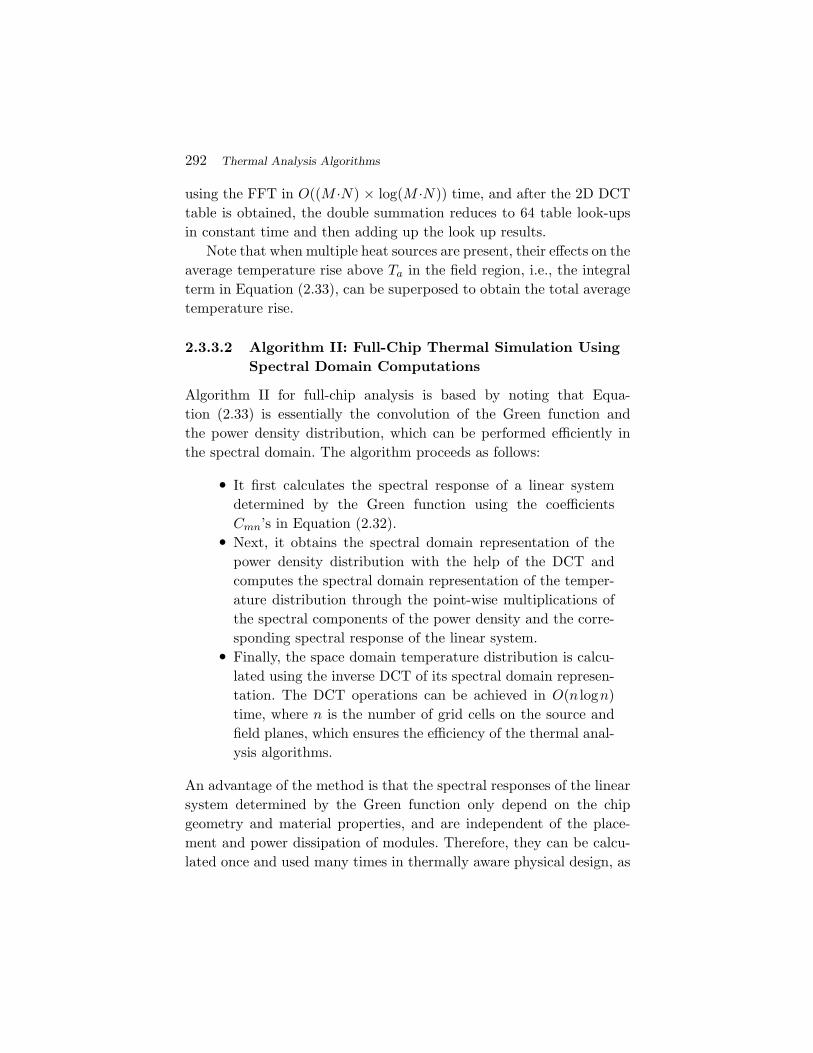
2.3.3.2 Algorithm II: Full-Chip Thermal Simulation UsingSpectral Domain Computations
Algorithm II for full-chip analysis is based by noting that Equa-tion (2.33) is essentially the convolution of the Green function andthe power density distribution, which can be performed efficiently inthe spectral domain. The algorithm proceeds as follows:
• It first calculates the spectral response of a linear systemdetermined by the Green function using the coefficientsCmn’s in Equation (2.32).
• Next, it obtains the spectral domain representation of thepower density distribution with the help of the DCT andcomputes the spectral domain representation of the temper-ature distribution through the point-wise multiplications ofthe spectral components of the power density and the corre-sponding spectral response of the linear system.
• Finally, the space domain temperature distribution is calcu-lated using the inverse DCT of its spectral domain represen-tation. The DCT operations can be achieved in O(n logn)time, where n is the number of grid cells on the source andfield planes, which ensures the efficiency of the thermal anal-ysis algorithms.
An advantage of the method is that the spectral responses of the linearsystem determined by the Green function only depend on the chipgeometry and material properties, and are independent of the place-ment and power dissipation of modules. Therefore, they can be calcu-lated once and used many times in thermally aware physical design, as
2.3 Steady-state Thermal Analysis Algorithms 293
the spatial configuration of the design is iteratively altered to achievean optimal layout.
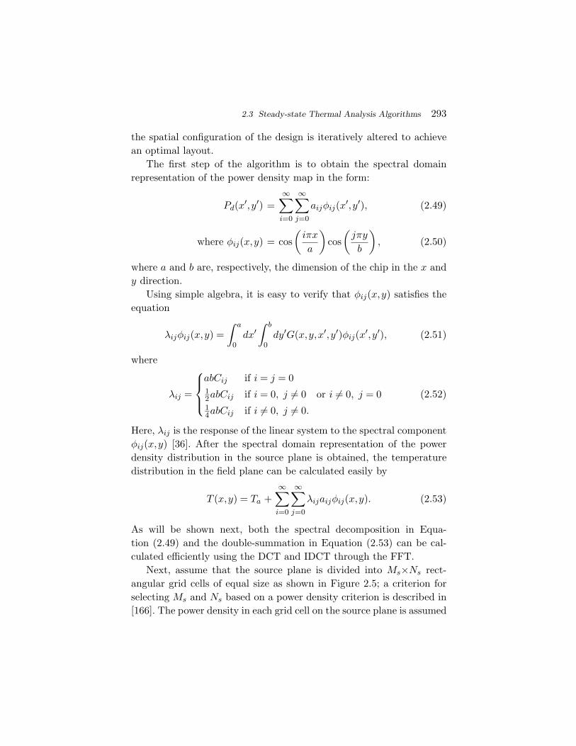
The first step of the algorithm is to obtain the spectral domainrepresentation of the power density map in the form:
Pd(x′,y′) =∞∑i=0
∞∑j=0
aijφij(x′,y′), (2.49)
where φij(x,y) = cos(
iπx
a
)cos(
jπy
b
), (2.50)
where a and b are, respectively, the dimension of the chip in the x andy direction.
Using simple algebra, it is easy to verify that φij(x,y) satisfies theequation
λijφij(x,y) =∫ a
0dx′∫ b
0dy′G(x,y,x′,y′)φij(x′,y′), (2.51)
where
λij =
abCij if i = j = 012abCij if i = 0, j �= 0 or i �= 0, j = 014abCij if i �= 0, j �= 0.
(2.52)
Here, λij is the response of the linear system to the spectral componentφij(x,y) [36]. After the spectral domain representation of the powerdensity distribution in the source plane is obtained, the temperaturedistribution in the field plane can be calculated easily by
T (x,y) = Ta +∞∑i=0
∞∑j=0
λijaijφij(x,y). (2.53)
As will be shown next, both the spectral decomposition in Equa-tion (2.49) and the double-summation in Equation (2.53) can be cal-culated efficiently using the DCT and IDCT through the FFT.
Next, assume that the source plane is divided into Ms×Ns rect-angular grid cells of equal size as shown in Figure 2.5; a criterion forselecting Ms and Ns based on a power density criterion is described in[166]. The power density in each grid cell on the source plane is assumed
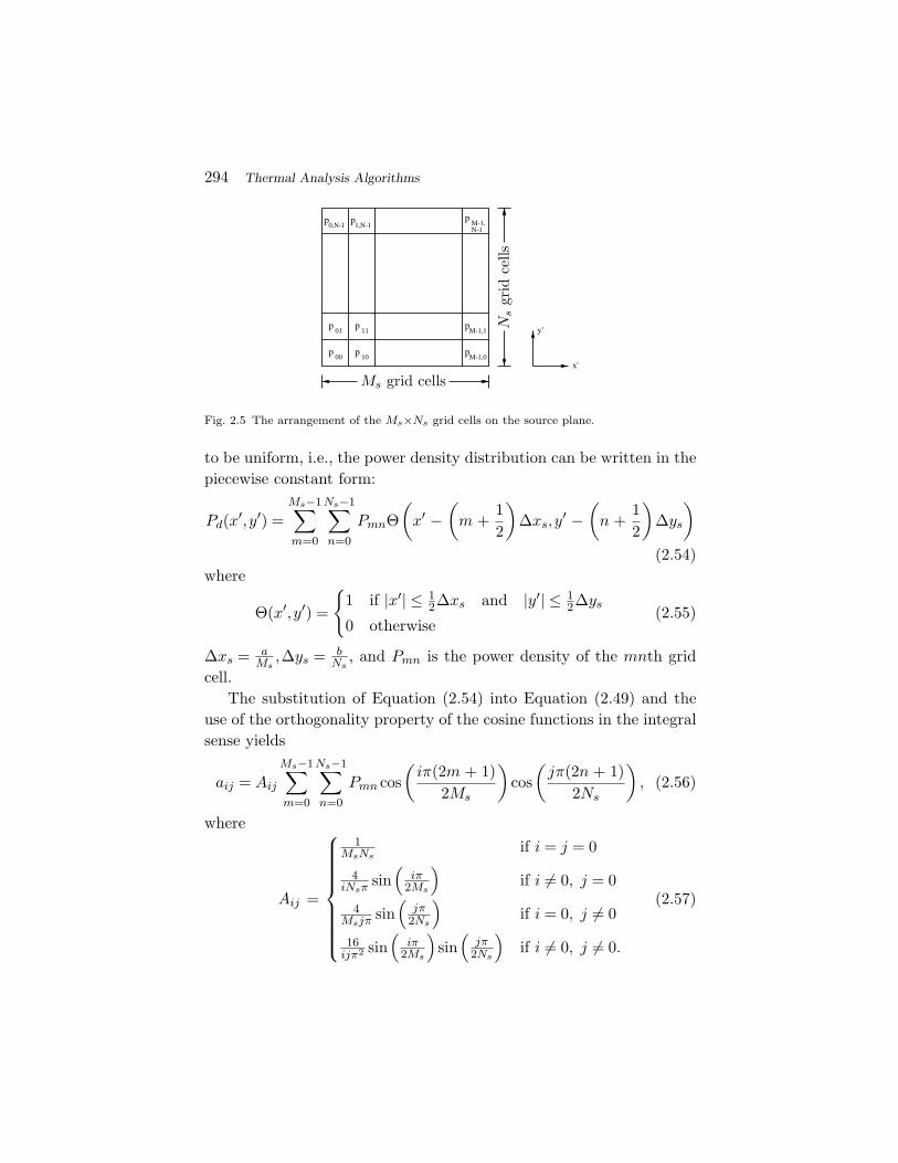
294 Thermal Analysis Algorithms
y'
x'
p
p
p
p
p p
p
p
p
M-1,0
M-1,1
10
1101
00
0,N-1 1,N-1 M-1,N-1
Fig. 2.5 The arrangement of the Ms×Ns grid cells on the source plane.
to be uniform, i.e., the power density distribution can be written in thepiecewise constant form:
Pd(x′,y′) =Ms−1∑m=0
Ns−1∑n=0
PmnΘ(
x′ −(
m +12
)∆xs,y
′ −(
n +12
)∆ys
)(2.54)
where
Θ(x′,y′) =
{1 if |x′| ≤ 1
2∆xs and |y′| ≤ 12∆ys
0 otherwise(2.55)
∆xs = aMs
,∆ys = bNs
, and Pmn is the power density of the mnth gridcell.
The substitution of Equation (2.54) into Equation (2.49) and theuse of the orthogonality property of the cosine functions in the integralsense yields
aij = Aij
Ms−1∑m=0
Ns−1∑n=0
Pmn cos(
iπ(2m + 1)2Ms
)cos(
jπ(2n + 1)2Ns
), (2.56)
where
Aij =
1MsNs
if i = j = 0
4iNsπ sin
(iπ
2Ms
)if i �= 0, j = 0
4Msjπ sin
(jπ
2Ns
)if i = 0, j �= 0
16ijπ2 sin
(iπ
2Ms
)sin(
jπ2Ns
)if i �= 0, j �= 0.
(2.57)

2.3 Steady-state Thermal Analysis Algorithms 295
As before, we see that for 0 ≤ i < Ms and 0 ≤ j < Ns, the doublesummation in Equation (2.56) can be considered as a term in the 2Dtype-II DCT [102] of the power density matrix P . For i ≥ Ms or j ≥ Ns,we can always find integers s1 and s2 such that i = 2s1Ms ± i andj = 2s2Ns ± j, where 0 ≤ i < Ms and 0 ≤ j < Ns.1 Hence, for any i
and j, we always have
aij = ±AijPij , (2.58)
where
Pij =Ms−1∑m=0
Ns−1∑n=0
Pmn cos
(iπ(2m + 1)
2Ms
)cos
(jπ(2n + 1)
2Ns
)(2.59)
with 0 ≤ i < Ms and 0 ≤ j < Ns is the 2D type-II DCT of the P matrixand the sign of the right-hand side of Equation (2.58) is determined bywhether s1 and s2 are even or odd numbers [36]. Equation (2.59) canbe calculated efficiently using the 2D FFT in O((Ms·Ns)× log(Ms·Ns))time. After the 2D DCT matrix P is obtained, the calculation of aij
simply involves computing the coefficient Aij and finding the corre-sponding term Pij .
From Equations (2.50) and (2.53), under the discretization, the tem-perature distribution T (x,y) can now be written as
T (x,y) = Ta +M ′−1∑i=0
N ′−1∑j=0
λijaij cos(
iπx
a
)cos(
jπy
b
). (2.60)
If we assume that the temperature field plane is divided into Mf×Nf
rectangular grid cells of equal size, then the average temperature of themnth grid cell can be obtained by
Tmn =1
∆xf∆yf
∫ (m+1)∆xf
m∆xf
dx
∫ (n+1)∆yf
n∆yf
dyT (x,y)
= Ta +M ′−1∑i=0
N ′−1∑j=0
Bij cos(iπ(2m + 1)
2Mf
)cos(jπ(2n + 1)
2Nf
), (2.61)
1 If i equals an odd multiple of Ms, we will not be able to write i as i = 2s1Ms ± i. However,for this kind of i, it can be easily shown that aij = 0 because cos
(iπ(2m+1)
2Ms
)= 0. Similarly,
we know that aij = 0 if j equals an odd multiple of Ns.

296 Thermal Analysis Algorithms
where ∆xf = aMf
, ∆yf = bNf
, and
Bij =
λijaij if i = j = 0
2λijaijMf
iπ sin(
iπ2Mf
)if i �= 0, j = 0
2λijaijNf
jπ sin(
jπ2Nf
)if i = 0, j �= 0
4λijaijMf Nf
ijπ2 sin(
iπ2Mf
)sin(
jπ2Nf
)if i �= 0, j �= 0.
(2.62)
Similar to the analysis shown previously, any i ≥ Mf and j ≥ Nf can
be written as i = 2s3Mf ± ˆi and j = 2s4Nf ± ˆj such that 0 ≤ ˆi < Mf ,
0 ≤ ˆj < Nf , and s3 and s4 are integers. Using the periodicity of thecosine function, we can finally cast Tmn into the form:
Tmn = Ta +Mf −1∑ˆi=0
Nf −1∑ˆj=0
Lˆiˆjcos
(ˆiπ(2m + 1)2Mf
)cos
( ˆjπ(2n + 1)2Nf
),
(2.63)where
Lˆiˆj=
B00 if ˆi = ˆj = 0∑i < M ′
i = 2s3Mf ± ˆi
± Bi0 if ˆi �= 0, ˆj = 0
∑j < N ′
j = 2s4Nf ± ˆj
± B0j if ˆi = 0, ˆj �= 0
∑i < M ′
i = 2s3Mf ± ˆi
∑j < N ′
j = 2s4Nf ± ˆj
± Bij if ˆi �= 0, ˆj �= 0
(2.64)
and the signs of the B′s in Equation (2.64) are determined by whethers3 and s4 are even or odd numbers. After the matrix L is obtained,the double summation in Equation (2.63) can be calculated efficientlyusing the 2D IDCT.
2.3 Steady-state Thermal Analysis Algorithms 297
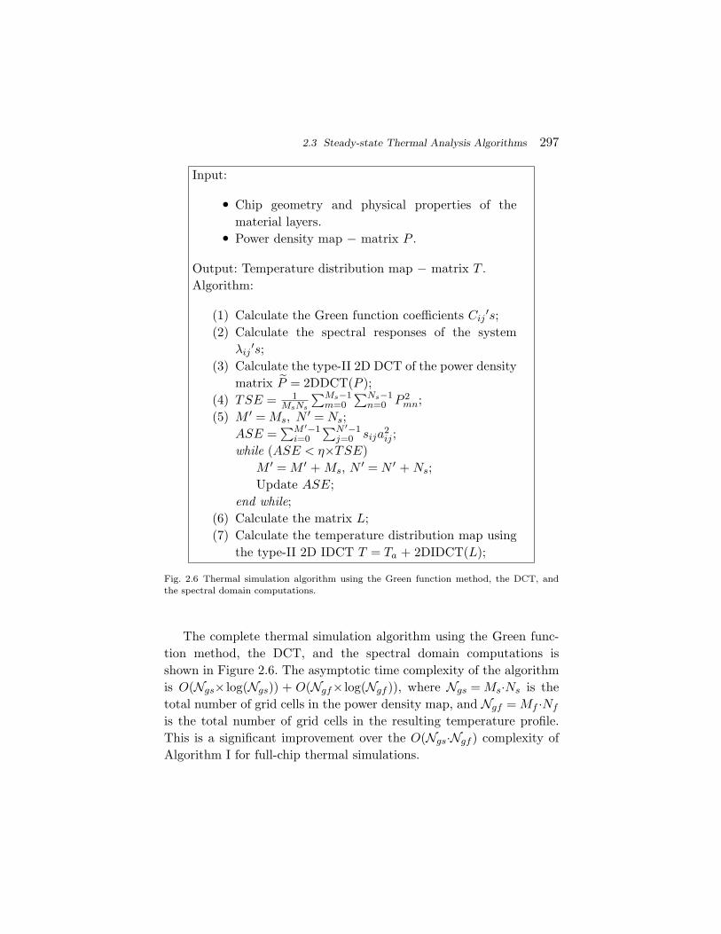
Input:
• Chip geometry and physical properties of thematerial layers.
• Power density map − matrix P .
Output: Temperature distribution map − matrix T .Algorithm:
(1) Calculate the Green function coefficients Cij′s;
(2) Calculate the spectral responses of the systemλij
′s;(3) Calculate the type-II 2D DCT of the power density
matrix P = 2DDCT(P );(4) TSE = 1
MsNs
∑Ms−1m=0
∑Ns−1n=0 P 2
mn;(5) M ′ = Ms, N ′ = Ns;
ASE =∑M ′−1
i=0∑N ′−1
j=0 sija2ij ;
while (ASE < η×TSE)M ′ = M ′ + Ms, N ′ = N ′ + Ns;Update ASE;
end while;(6) Calculate the matrix L;(7) Calculate the temperature distribution map using
the type-II 2D IDCT T = Ta + 2DIDCT(L);
Fig. 2.6 Thermal simulation algorithm using the Green function method, the DCT, andthe spectral domain computations.
The complete thermal simulation algorithm using the Green func-tion method, the DCT, and the spectral domain computations isshown in Figure 2.6. The asymptotic time complexity of the algorithmis O(Ngs× log(Ngs)) + O(Ngf× log(Ngf )), where Ngs = Ms·Ns is thetotal number of grid cells in the power density map, and Ngf = Mf ·Nf
is the total number of grid cells in the resulting temperature profile.This is a significant improvement over the O(Ngs·Ngf ) complexity ofAlgorithm I for full-chip thermal simulations.
298 Thermal Analysis Algorithms
2.3.3.3 Algorithm III: Thermal Simulation with LocalHigh Accuracy Requirements
In some cases, a design may have different requirements on the accuracyof the thermal simulation over different parts of the same chip. Forexample, in mixed signal designs where analog circuits are fabricatedon the same chip as digital circuits, the analog blocks often have morestringent accuracy requirements on the thermal simulation because theoperations of the analog circuits are more sensitive to temperature. Forfull-chip analysis, Algorithm I will be too slow, and Algorithm II willconstrain the size of each grid cell to be small enough to satisfy thehighest accuracy requirements, resulting in wasted computation.
The key idea of Algorithm III is to use coarse grids to divide thesource and field planes, so that the size of each grid cell in the fieldplane satisfies the accuracy requirements of the digital circuits. A tem-perature analysis is performed using Algorithm II to perform thermalanalysis at a level of accuracy that is sufficient for most blocks (e.g.,for all the digital blocks in a design). Finally, for each region or unit onthe field plane whose temperature is to be calculated more accurately(e.g., the analog blocks), we use Algorithm I to compute the contri-butions to its temperature rise from the nearby logic gates and analogfunction units on the source plane, and use this result to correct thetemperature obtained by Algorithm II over the coarse grid cell.
2.3.4 Comparison Between Steady-StateThermal Analysis Algorithms
We have presented three different classes of steady-state thermal anal-ysis algorithms, and they each have their own advantages and disad-vantages. The FDM and FEM are more generic, and they can handlecomplicated on-chip geometries such as nonuniform wiring structures.Therefore, they can achieve very high accuracy in thermal analysis.However, the direct application of these two methods usually involvesmeshing the entire substrate, which may lead to large problem sizes andrelatively long runtimes. Using the macromodeling techniques such asthat presented in [139], it is possible to abstract away the nodes thatthe user of the thermal simulator is not interested in, and therefore,

2.4 Solving the Linear Equations 299
reduce the problem sizes in the finite difference and finite elementanalysis. However, building a macromodel still involves considerableeffort. Therefore, the macromodeling approach is most effective underthe situation where the chip geometry does not change but the thermalanalysis needs to be performed multiple times, such as in the fixed-diethermal aware floorplanning and placement, because the time it takesto build the macromodel can be amortized.
In Green function-based methods, only the layers where the temper-ature distribution is to be calculated and the layers where the power isgenerated are meshed. Therefore, the resulting problem size is relativelysmall and the efficiency of thermal analysis is rather high. However, ina Green function-based thermal analysis, it is often assumed that thechip materials are layer-wise uniform, which may be too restrictive. Asa result, these algorithms are usually used in early stages of physicaldesign, where the accuracy requirement on thermal analysis is moder-ate but the efficiency requirement is high.
2.4 Solving the Linear Equations
The FEM and FDM methods both lead to problem formulations thatrequire the solution of large systems of linear equations. The matricesthat describe these equations are typically sparse (more so for the FDMthan the FEM, as can be seen from the individual element stamps) andpositive definite.
There are many different ways of solving these equations. Directmethods typically use variants of Gaussian elimination, such as LUfactorization, to first factor the matrices, and then solve the systemthrough forward and backward substitution. The cost of LU factoriza-tion is O(n3) for a dense n × n matrix, but is just slightly superlinear inpractice for sparse systems. This step is followed by forward/backwardsubstitution, which can be performed in O(n) time for a sparse systemwhere the number of entries per row is bounded by a constant. If asystem is to be evaluated for a large number of right-hand side vectors,corresponding to different power vectors, LU factorization only needsto be performed once and its cost may be amortized over the solutionfor multiple input vectors.

300 Thermal Analysis Algorithms
Iterative methods are seen to be very effective for large sparse pos-itive definite matrices. This class of techniques includes more classicalmethods such as Gauss–Jacobi, Gauss–Seidel, and successive overrelax-ation, as well as more contemporary approaches based on the conjugategradient method or GMRES. The idea here is to begin with an ini-tial guess solution, and to successively refine it to achieve convergence.Under certain circumstances, it is possible to guarantee this conver-gence: in particular, FDM matrices have a structure that guaranteesthis property. For further details on standard techniques used in directand iterative solvers, the reader is referred to a standard text on thetopic, such as [47].
In this section, we will focus on describing two methods that areespecially useful in solving thermal systems, namely, the multigridapproach and the random walk method. Our exposition will describeboth of these in the context of the FDM. It should be noted that thesemethods are also useful in solving transient analysis problems undertime-stepping, as outlined in Section 2.5.
2.4.1 The Multigrid Method
The multigrid algorithm was successfully used in [83, 84] to solvethe thermal analysis problem using the FDM matrices. The multi-grid method follows a hierarchical approach to solve the thermal prob-lem and has been used in the solution of a number of areas wherethe underlying problem is described by a PDE or is equivalent toits discretization (e.g., in the solution of on-chip power grids). Anexcellent tutorial on various aspects of the multigrid method can befound in [15]. The essence of the approach is based on the observa-tion that an iterative solver is usually more effective in removing highfrequency solution errors in an FDM mesh than low frequency errors.Therefore, the method constructs a hierarchy of FDM meshes corre-sponding to the thermal problem, with each lower level mesh beingcoarser than the adjacent higher level mesh in the hierarchy. The solverstarts with iterating over the finest mesh, and once it detects thatthe speed toward convergence is slowed down due to low frequencysolution errors, the iteration is changed to the coarser grid that is
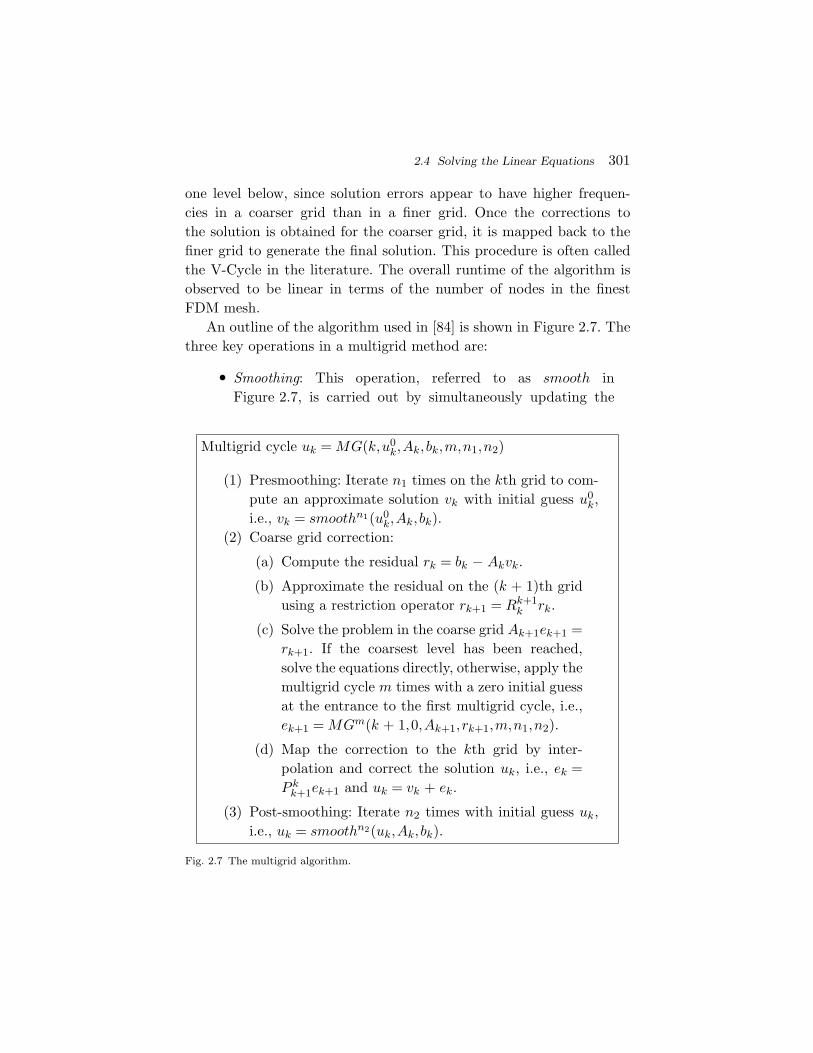
2.4 Solving the Linear Equations 301
one level below, since solution errors appear to have higher frequen-cies in a coarser grid than in a finer grid. Once the corrections tothe solution is obtained for the coarser grid, it is mapped back to thefiner grid to generate the final solution. This procedure is often calledthe V-Cycle in the literature. The overall runtime of the algorithm isobserved to be linear in terms of the number of nodes in the finestFDM mesh.
An outline of the algorithm used in [84] is shown in Figure 2.7. Thethree key operations in a multigrid method are:
• Smoothing: This operation, referred to as smooth inFigure 2.7, is carried out by simultaneously updating the
Multigrid cycle uk = MG(k,u0k,Ak, bk,m,n1,n2)
(1) Presmoothing: Iterate n1 times on the kth grid to com-pute an approximate solution vk with initial guess u0
k,i.e., vk = smoothn1(u0
k,Ak, bk).(2) Coarse grid correction:
(a) Compute the residual rk = bk − Akvk.
(b) Approximate the residual on the (k + 1)th gridusing a restriction operator rk+1 = Rk+1
k rk.
(c) Solve the problem in the coarse grid Ak+1ek+1 =rk+1. If the coarsest level has been reached,solve the equations directly, otherwise, apply themultigrid cycle m times with a zero initial guessat the entrance to the first multigrid cycle, i.e.,ek+1 = MGm(k + 1,0,Ak+1, rk+1,m,n1,n2).
(d) Map the correction to the kth grid by inter-polation and correct the solution uk, i.e., ek =P k
k+1ek+1 and uk = vk + ek.
(3) Post-smoothing: Iterate n2 times with initial guess uk,i.e., uk = smoothn2(uk,Ak, bk).
Fig. 2.7 The multigrid algorithm.

302 Thermal Analysis Algorithms
Fig. 2.8 One step in a smoothing iteration which involves updating the temperature corre-sponding to one column of the FDM cells.
values of the unknowns corresponding to a vertical columnof nodes in the FDM mesh, as shown in Figure 2.8, in eachstep of a smoothing iteration. A conventional smoothingoperation could use a few Gauss–Seidel iterations, forexample, but this approach takes advantage of the factthat heat flow in the z direction dominates flow in the x
or y dimensions under typical discretization schemes. Themodified smoothing operation involves the solution of atridiagonal linear system (as each node is linked to the nodeabove and below it), which has a linear runtime in terms ofthe dimension of the system.
• Restriction: The restriction operator, Rk+1, maps a finergrid at level k to a coarser grid at level k + 1. Mathemati-cally, this involves finding the residual rk+1 in the (k + 1)thgrid given the residual rk in the kth grid, and in [84],the component of the residual at a particular node in the(k + 1)th grid is obtained by taking the weighted averageof the residual components corresponding to the samenode and its neighboring nodes in the kth grid, where theweight of each point is the absolute value of its coefficientin the finite difference equations corresponding to thekth grid.
• Interpolation: The role of the interpolation operator, P k+1,is to map a coarser grid at level k + 1 to a finer grid at levelk. It finds the error correction term ek in the fine grid, giventhe correction term ek+1 in the coarse grid, and in [84], this

2.4 Solving the Linear Equations 303
is achieved by setting
ekp,q,r =
1A
(ap−1,q,re
kp−1,q,r + ap+1,q,re
kp+1,q,r + ap,q−1,re
kp,q−1,r
+ap,q+1,rekp,q+1,r + ap,q,r−1e
kp,q,r−1 + ap,q,r+1e
kp,q,r+1
),
(2.65)
where ekp,q,r is the component of ek that corresponds to the
(p,q,r)th node in the FDM mesh, ap,q,r is the coefficient ofthe FDM equations that is determined by the material prop-erties of the chip and the discretization, and A = ap−1,q,r +ap+1,q,r + ap,q−1,r + ap,q+1,r + ap,q,r−1 + ap,q,r+1 Here, p, q,and r are the indices of the node in the x, y, and z directions,respectively. Note that the weighted averaging using theai,j,k values, rather than a simple averaging, serve to captureeffects related to anisotropies in thermal conductivity.
2.4.2 The Random Walk Method
The random walk method has been used in the literature to solve theon-chip power grid analysis problem, which is structurally identical tothe thermal analysis problem using finite differences. It involves thesolution of a network of resistors, constant current sources, and con-stant voltage sources, and computes the voltage throughout this circuit,which corresponds to temperature under the thermal–electrical anal-ogy, defined in Section 2.3.1. The random walk method has been usedsuccessfully in the solution of such large networks. These techniquesperform very well when the temperatures at one node, or a small num-ber of nodes, must be calculated. Therefore, a major benefit of thesemethods is in their ability to perform incremental analysis rapidly andefficiently, and they are good for computing the effects of a small designchange that requires temperature changes in only a small region ofthe chip.
To outline the method, we will consider the solution of a resistivenetwork for the voltages; the thermal analog, of course, is that thevoltages in the resistive network are the temperatures, and the currentsources are the power values.

304 Thermal Analysis Algorithms
3
2
4
x
Ix
g2
g4
g3g1
1
Fig. 2.9 A representative node in the resistive network.
For the DC analysis of a resistive network with constant currentand voltage sources, let us look at a single node x in the circuit, asillustrated in Figure 2.9. The application of Kirchoff’s Current Law,Kirchoff’s Voltage Law, and the device equations for the conductances,yields the following equation:
degree(x)∑i=1
gi(Vi − Vx) = Ix, (2.66)
where the nodes adjacent to x are labeled 1,2, . . . , degree(x), Vx is thevoltage at node x, Vi is the voltage at node i, gi is the conductancebetween node i and node x, and Ix is the current load connected tonode x. Equation (2.66) can be reformulated as follows:
Vx =degree(x)∑
i=1
gi∑degree(x)j=1 gj
Vi − Ix∑degree(x)j=1 gj
. (2.67)
This implies that the voltage at any node is a linear function of thevoltages at its neighbors. We also observe that the sum of the linearcoefficients associated with the Vi’s is 1. For a resistive network withN nodes at nonfixed voltage values we have N linear equations similarto the one above, one for each node. Solving this set of equations,

2.4 Solving the Linear Equations 305
along with the condition that the voltage at a fixed node h is theconstant value Vh, provides the exact solution. In thermal analysis,the fixed node could correspond to the ambient, which is at a fixedtemperature. Alternatively, if a package model is provided, it can beappended to the FDM circuit, with some node(s) of the package modelbeing connected to the ambient, and the combined circuit can be solvedto obtain temperatures within the structure.
Having considered the resistive circuit problem, let us construct arandom walk “game,” given a finite undirected connected graph (forexample, Figure 2.10) representing a street map. A walker starts fromone of the nodes, and goes to an adjacent node i every day with prob-ability px,i for i = 1,2, . . . ,degree(x), where x is the current node, anddegree(x) is the number of edges connected to node x. These probabil-ities satisfy the following relationship:
degree(x)∑i=1
px,i = 1. (2.68)
The walker pays an amount mx to a motel for lodging everyday, untilhe/she reaches one of the homes, which are a subset of the nodes. Ifthe walker reaches the home h, he/she will stay there and be awardeda certain amount of money, m0h; note that this value can be differentat different homes. We will consider the problem of calculating the
Fig. 2.10 An instance of a random walk “game.”
306 Thermal Analysis Algorithms
expected amount of money that the walker has accumulated at the endof the walk, as a function of the starting node, assuming he/she startswith nothing. The gain function for the walk is therefore defined as
f(x) = E[total money earned|walk starts at node x]. (2.69)
It is obvious that
f(one of the homes) = m0h. (2.70)
For a nonhome node x, assuming that the nodes adjacent to x arelabeled 1,2, . . . ,degree(x), the f variables satisfy
f(x) =degree(x)∑
i=1
px,if(i) − mx. (2.71)
For a random-walk problem with N nonhome nodes, there are N lin-ear equations similar to the one above, and the solution to this set ofequations will give the exact values of f at all nodes.
It is easy to draw a parallel between this problem and that of resis-tive network analysis. Equation (2.71) becomes identical to (2.67), andEquation (2.70) reduces to the condition of constant voltage sources.
px,i =gi∑degree(x)
j=1 gj
i = 1,2, . . . ,degree(x)
mx =Ix∑degree(x)
j=1 gj
m0h = Vh, f(x) = Vx. (2.72)
In other words, for any resistive network problem, we can constructa random walk problem that is mathematically equivalent, i.e., char-acterized by the same set of equations. It can be proven that such anequation set has and only has one unique solution [41]. Therefore, ifwe find an approximated solution for the random walk, it is also anapproximated solution for the resistive network.
A natural way to approach the random walk problem is to perform acertain number of experiments and use the average money left in thoseexperiments as the approximated solution. If this amount is averagedover a sufficiently large number of walks by playing the “game” a suf-ficiently large number of times, then by the law of large numbers, an

2.5 Transient Thermal Analysis 307
acceptably accurate solution can be obtained, and the error can beestimated using the Central Limit Theorem [164].
A desirable feature of the proposed algorithm is that it localizes thecomputation, i.e., it can calculate a single node voltage without havingto solve the whole circuit. As compared to a conventional approachthat must solve the full set of matrix equations to find the voltage atany one node, the computational advantage of this method could betremendous. Numerous efficiency enhancing techniques are available forthis approach, and are described in further detail in [112, 114].
Another version of this approach uses the random walk solver toobtain a high-quality preconditioner for an iterative method. The essen-tial idea is that the information gathered during the random walks,when organized well, can be used to generate approximate LU factorsat almost no additional cost. These approximate LU factors may thenbe used to generate a preconditioner, whose quality is shown to besuperior to many existing methods [111, 113].
2.5 Transient Thermal Analysis
In this section, we will provide an outline of approaches that maybe used for transient analysis. Our description will primarily focuson FDM-based formulations, since these are most widely used in theIC world today. However, it is understood that equivalent approachesmay also be used under other methods, typically using a timestepping-based approach. Alternatively, it is possible to use frequency-domaintechniques [163], as is common in the case of analyzing transients inelectrical circuits.
For transient thermal analysis, the time-dependent left-hand sideterm in Equation (2.3) is nonzero. Using a similar finite differencingstrategy as in Section 2.3.1, the equation may be discretized in thespace domain as
ρcp∂Ti,j,k
∂t= kt
[δ2xTn+1
i,j,k + δ2xTn
i,j,k
2(∆x)2+
δ2yT
n+1i,j,k + δ2
yTni,j,k
2(∆y)2
+δ2zT
n+1i,j,k + δ2
zTni,j,k
2(∆z)2
]+
gni,j,k
ρcp. (2.73)

308 Thermal Analysis Algorithms
Again, using similar substitutions as in Section 2.3.1, the time-independent terms on the right-hand side can again be considered tobe the currents per unit volume through thermal resistors and thermalcurrent sources. The left-hand side, on the other hand, represents a cur-rent source of value ρcp
∂Ti,j,k
∂t . Recalling that in the thermal–electricalanalogy, the temperatures correspond to voltages, it is easy to see thatwe can represent the left-hand side by a thermal capacitor of value ρcp
per unit volume.Given this mapping, transient thermal analysis can be performed by
creating the equivalent network consisting of resistors, current sources,and capacitors, and using routine electrical techniques for transientanalysis.
2.5.1 The ADI Method
An alternative iterative approach that is often used in the heat transfercontext is the so-called alternating-direction-implicit (ADI) method.This method is described in standard texts on heat transfer, and wasemployed in [151] for on-chip transient thermal analysis. The left-handside of Equation (2.73) is discretized with respect to the time variablet to obtain
Tn+1i,j,k − Tn
i,j,k
∆t. (2.74)
The work in [151] adopted the Crank–Nicholson method for discretizingEquation (2.3), which uses the centered finite difference in space andthe trapezoidal rule in time (see Figure 2.11).
Fig. 2.11 The node indexing scheme for the spatial discretization.

2.5 Transient Thermal Analysis 309
(a) (b)
Fig. 2.12 The nonzero patterns of the coefficient matrices. (a) The coefficient matrix forsolving the discretized PDE directly. (b) The coefficient matrix in each sub-step of the ADIalgorithm.
The objective is to solve for Tn+1i,j,k for all i, j,k assuming that Tn
i,j,k’sare known. Then through time marching, the evolution of the tempera-ture distribution as a function of time can be obtained. It is not difficultto see that if we number the nodes in a lexicographical order and collectthe linear equations associated with each node, the resulting coefficientmatrix of the equations will be sparse and banded, as shown in Fig-ure 2.12(a). However, solving this system of linear equations directlytakes super-linear time. To improve the overall efficiency of thermalanalysis, the authors of [151] adopted an ADI algorithm to solve Equa-tion (2.73). Specifically, each time step is split into three sub-steps, andin each sub-step, a system of finite difference equations that is implicitin only one spatial direction is constructed, as shown below.
Step I:
Tn+(1/3)i,j,k − Tn
i,j,k =rxδ2
x
2(T
n+(1/3)i,j,k + Tn
i,j,k
)+ryδ
2yT
ni,j,k + rzδ
2zT
ni,j,k +
∆t
ρcpgni,j,k (2.75)
Step II:
Tn+(2/3)i,j,k − Tn
i,j,k =rxδ2
x
2(T
n+(1/3)i,j,k + Tn
i,j,k
)+
ryδ2y
2(T
n+(2/3)i,j,k + Tn
i,j,k
)+rzδ
2zT
ni,j,k +
∆t
ρcpgni,j,k (2.76)

310 Thermal Analysis Algorithms
Step III:
Tn+1i,j,k − Tn
i,j,k =rxδ2
x
2(Tn+(1/3)
i,j,k + Tni,j,k)
+ryδ
2y
2(T
n+(2/3)i,j,k + Tn
i,j,k
)+
rzδ2z
2(Tn+1
i,j,k + Tni,j,k
)+
∆t
ρcpgni,j,k, (2.77)
where
rx =kt∆t
ρcp
1∆x2 , ry =
kt∆t
ρcp
1∆y2 , rz =
kt∆t
ρcp
1∆z2 . (2.78)
The unknowns in the three sub-steps are Tn+(1+3)i,j,k ’s, T
n+(2/3)i,j,k ’s, and
Tn+1i,j,k ’s, respectively. It can be seen that the coefficient matrix of the
finite difference equations in each of the sub-steps is tridiagonal asshown in Figure 2.12(b), and tridiagonal linear systems can be solved inlinear time. As a result, the overall runtime of performing the transientthermal analysis via the ADI approach is O(ns), where n is the totalnumber of nodes in the finite difference mesh and s is the number oftime steps.
2.5.2 HotSpot: An Approach for Architectural-LevelTransient Analysis
The work in [135] first proposed HotSpot, a technique for architectural-level thermal analysis that can be coupled to architectural simulators.Subsequently, several updates and elaborations on the approach havebeen outlined in [60, 61, 62, 63, 64, 134], and a public-domain releaseof the tools is available [1] and widely used. The goal of this approachis to obtain a coarsely discretized FDM solution to the on-chip thermalproblem, with an FDM/FEM-like model for the package components.This coarse granularity is appropriate at the architectural level, wherethe power of large functional blocks can be estimated, but details ofthe design are as yet unknown. Thermal analysis at this stage canbe linked to a cycle-accurate architectural power estimation tool suchas Wattch [16]. Such an approach can be extremely useful in makingthermally conscious decisions at the architectural level.

2.5 Transient Thermal Analysis 311
Fig. 2.13 An RC model of the chip, used in HotSpot [134].
The thermal model used in HotSpot is an RC model, illustrated inFigure 2.13. Depending on the accuracy desired, the chip area may bemodeled using an FDM approach where the discretization correspondseither to (i) a grid of regions, the center of each of which is a node inthe thermal network, such that the power dissipation of each block isassumed to be uniformly distributed over the grid points that it covers,or (ii) a set of rectangular regions corresponding to functional blocks,where the center of each functional block corresponds to a node (insubsequent versions of HotSpot, blocks with skewed aspect ratios aredivided into subblocks whose aspect ratios are closer to 1:1). The heatspreader is divided into five blocks, one directly below the die, andfour trapezoids corresponding to the peripheral region that is not cov-ered by the die; likewise, the heat sink is also divided into five blocks,

312 Thermal Analysis Algorithms
corresponding to the area under the spreader and four similarly con-structed external trapezoids. Within each layer, lateral conduction iscaptured by resistors between adjacent blocks, and vertical conductionis modeled by a resistance between each block and the block(s) adja-cent to it in an adjoining layer. A thermal capacitance is connected toeach node in the circuit, the heat sink is assumed to be connected tothe ambient, and the power sources correspond to the power associatedwith each functional block on the die. Both the primary heat flow paththrough the heat sink, and the secondary heat flow path, through theCBGA grid and the PCB, are modeled.
Interconnect effects are captured by modeling the self-heating effectsof wires, and using Rent’s rule-based wire density predictions on eachlayer to obtain an effective thermal conductivity for the region arounda wire. The composite thermal RC system is solved using a fourth-order Runge–Kutta method at each time step, to obtain the result ofa transient analysis.
3Effects on Circuit Performance
In this survey, we will consider the effect of elevated on-chip tempera-tures on circuit performance. Specifically, we will address the issue ofthermal effects on circuit delay, power, and reliability.
3.1 Circuit Delay as a Function of Temperature
Increases in temperature can affect the parameters of both transistorsand on-chip interconnects, thus affecting the circuit delay. Thermalvariations can affect transistor behavior in two ways:
• The mobility, µ, of charge carriers in a transistor reduceswith increasing temperature, T , according to the equation
µ(T ) = µ(T0)(
T
T0
)−m
, (3.1)
where T0 is room temperature (typically, 300 K), and m > 0is the mobility temperature exponent, with a typical value of1.7 in highly doped silicon, and 1.4 in nanometer-thin siliconlayers, where boundary scattering becomes important [109].This reduction in the mobility lowers the drive current of
313

314 Effects on Circuit Performance
a transistor, leading to a tendency toward increased delayswith increasing temperatures.
• The threshold voltage of a transistor, Vth, decreases withincreasing temperature along the trajectory
Vth(T ) = Vth(T0) − κ(T − T0), (3.2)
where κ > 0 is the threshold voltage temperature coefficientwith a typical value of 2.5 mV/K [74]. This trend makes iteasier for a transistor to switch on as temperatures rise, andimplies a tendency for an increased drive current. Therefore,this effect results in a reduction in the circuit delay withincreasing temperatures.
The two effects above are in contradiction, and depending on whichof the two is more dominant, one may see either negative tempera-ture dependence, where delays increase with temperature, or positivetemperature dependence, where delays decrease with temperature. Itis also possible that neither effect will dominate over the entire rangeof temperatures, implying that there may be nonmonotonic behaviorin the delay-temperature curve: this corresponds to mixed temperaturedependence. Issues related to mixed/inverted temperature dependencehave been addressed in [39, 45, 74].
Interconnect parameters are also affected by thermal effects. Theresistance, R, of a wire segment increases with temperature as follows:
R = R0(1 + β(T − T0)), (3.3)
where R0 is the resistance of the wire at room temperature, T0. Thevalue of β is typically positive, and this implies that the RC delayof a wire typically increases with temperature. Moreover, since wiresoften travel through large lengths of insulating media, the heat gen-erated in a wire can result in localized self-heating, or Joule-heating,effects [9].
3.2 The Leakage–Temperature Relationship
The power dissipated in a circuit consists of three components: dynamicpower due to the charging/discharging of parasitic capacitances,

3.2 The Leakage–Temperature Relationship 315
short-circuit power due to crowbar current from supply to ground dur-ing switching, and static power due to leakage when a transistor issupposedly off. The first two of these are less significantly impacted bytemperature, but leakage power has a large temperature dependence.Leakage is now one of the dominant components of the total on-chippower: reported results show cases where more than half of the totalpower dissipation is due to leakage, and therefore, this is a seriousissue. Moreover, leakage is susceptible to process variations [20] andtemperature variations [37], which are magnified by the exponentialterms associated with various components of leakage, as we will seebelow.
There are two major constituents of leakage current: subthresh-old leakage current and gate tunneling current [122]. The subthresholdleakage current is the leakage current between the drain and sourcenode when the device is in the “off” state (the voltage between thegate and source terminal is zero). Historically, in 0.25µm and highertechnology nodes, the subthreshold leakage was small enough to benegligible (several orders of magnitude smaller than the on-current).However, the traditional scaling requires the reduction of supply volt-age VDD, along with the reduction of the channel length. As a conse-quence, the threshold voltage must be scaled accordingly in order tomaintain the driving capability of the MOSFET device. Even thoughthis scaling has not been linear, because of leakage considerations, thescaled threshold voltage increases the proportion of the subthresholdleakage current to the total current. Therefore, subthreshold leakage isa significant factor in nanometer technologies.
The second component of the static power is the gate tunnelingcurrent, which is also a consequence of scaling. As the device dimen-sions are reduced, the gate oxide thickness also must be reduced. Anunwanted consequence of thinner gate oxide thickness is the increasedgate tunneling leakage current. Compared to the exponential depen-dence of subthreshold leakage on temperature, gate leakage is lessaffected by temperature. Moreover, the recent introduction of high-k gate dielectrics is likely to control the gate leakage problem, at leastfor a few generations.

316 Effects on Circuit Performance
An expression for the subthreshold leakage current density, i.e., thecurrent per unit transistor area, is given by Mukhopadhyay et al. [95]:
Jsub =W
Leffµ
√qεsiNcheff
2φsv2T exp
(Vgs − Vth
ηvT
)[1 − exp
(−Vds
vT
)].
(3.4)The details of the parameters in the above equation can be found in[95], but it is important to make a few observations:
• The term vT = kT/q is the thermal voltage, where k is theBoltzmann’s constant and q is the electrical charge, and T
is the junction temperature. From the equation, we can seethat the leakage is an exponential function of the junctiontemperature T .
• The symbol Vth represents the threshold voltage. It can beshown that for a given technology, Vth is a function of theeffective channel length Leff . Therefore, subthreshold leakageis also an exponential function of effective channel length.
• The drain-to-source voltage, Vds, is closely related to supplyvoltage VDD , and has the same range in static CMOS circuits.Therefore, subthreshold leakage is an exponential function ofthe supply voltage.
• The threshold voltage Vth is also affected by the body biasVBS . In a bulk CMOS technology, since the body nodeis always tied to ground for NMOS and VDD for PMOS,the body bias conditions for stacked devices are different,depending on the location of the “off” device on a stack (e.g.,top of the stack or bottom of the stack). As a result, the sub-threshold leakage current can vary quite significantly whendifferent input vectors are applied to a gate with stacks.
For the gate tunneling current, a widely used model is the one pro-vided in [14]:
Jtunnel =4πm∗q
h3 (kT )2(
1 +γkT
2√
EB
)exp(
EF0,Si/SiO2
kT
)exp(−γ
√EB),
(3.5)

3.2 The Leakage–Temperature Relationship 317
where T is the operating temperature, EF0,Si/SiO2 is the Fermi levelat the Si/SiO2 interface and m∗ depends on the underlying tun-neling mechanism. Parameters k and q are defined as above, and h
is Planck’s constant: all of these are physical constants. The termγ = 4πtox
√2mOX/h, where tox is the oxide thickness, and mox is the
effective electron mass in the oxide. The parameter EB is the height ofthe energy barrier, given by
EB = q
(ξ − Vox
2
), (3.6)
where ξ is the modified electron affinity in silicon, and Vox is the appliedvoltage across the oxide.
Besides physical constants and many technology-dependent param-eters, it is quite clear that the gate-tunneling leakage depends on thegate oxide thickness and the operating temperature. The former is astrong dependence, but the latter is more complex: over normal rangesof operating temperature, the variations in gate leakage are roughly lin-ear. In comparison with subthreshold leakage, which shows exponentialchanges with temperature, these gate leakage variations are often muchlower. More details about this model can be found in [14].
One possible solution to mitigate the negative impact of gate currentis to use material with higher dielectric constants (i.e., high-k material)in conjunction with metal gates [81]. In many current technologies, thegate leakage component is non-negligible. Recently some progress hasbeen reported on the development of high-k material. If successfullydeployed, the new technology can reduce gate tunneling leakage by atleast an order of magnitude, and at least postpone the point at whichgate leakage becomes significant.
Due to the power consumption limit dictated by the air-coolingtechnique widely accepted by the industry and market, power consump-tion, especially static power, has become a major design constraint.Besides the advancements in manufacturing technology and materialscience, several circuit level power reduction techniques also have impli-cations on the physical design flow. They include power gating, Vth
(or effective channel length) assignment, input vector assignment or

318 Effects on Circuit Performance
any combination of these methods. More details on these topics can befound in [82, 96, 122].
3.3 Reliability and Aging Effects
Thermal effects can cause a circuit to age prematurely. In this section,we present an outline of a few reliability effects that are exacerbated bythermal stress, namely, bias temperature instability, oxide breakdown,and electromigration.
3.3.1 Bias Temperature Instability
Bias temperature instability is a phenomenon that causes thresholdvoltage shifts over long periods of time, eventually causing the circuitto fail to meet its specifications. The word “bias” refers to the fact thatthis degradation is heightened by the application of a bias on the gatenode of a transistor.
The phenomenon of negative bias temperature instability (NBTI)can be illustrated with the help of a simple circuit, an inverter, illus-trated in Figure 3.1(a). When a PMOS transistor is biased in inversion(Vgs = −Vdd) (for example, when the input of the inverter is at logic0), interface traps are generated due to the dissociation of Si–H bondsalong the substrate-oxide interface, as illustrated in Figure 3.1(b). Theconnection of this mechanism to thermal effects is that the rate ofgeneration of these traps is accelerated by elevated temperatures, and
Fig. 3.1 (a) An inverter whose PMOS device is alternately subjected to NBTI stress andrelax phases. (b) An illustration of the phenomenon of NBTI.
3.3 Reliability and Aging Effects 319
therefore, increased on-chip temperatures can directly affect the life-time of a chip. The time for which the transistor is stressed is anotherfactor that increases the level of degradation. These traps cause anincrease in the threshold voltage (Vth), and a reduction in the saturationcurrent (Idsat) of the PMOS transistors. This effect, known as NBTI,has become a significant reliability issue in high-performance digital ICdesign, especially in sub-130 nm technologies [5, 19, 75, 91, 116, 128]. Anincrease in Vth causes the circuit delay to degrade, and when this degra-dation exceeds a certain amount, the circuit may fail to meet its timingspecifications. The rate constants of the reactions that define NBTI aredependent on temperature, and are worsened at elevated temperatures.
A corresponding and dual effect, known as Positive Bias Temper-ature Instability (PBTI) can be seen for NMOS devices, for example,when the input to an inverter is at logic 1, and a positive bias stressis applied across the gate oxide of the NMOS device. Although theimpact of a stressing bias on PBTI is lower than NBTI [116], PBTI isbecoming increasingly important in its own right. Moreover, techniquesare developed to reduce NBTI can contribute to increasing PBTI. Forexample, for the example of the inverter listed earlier, if the input isbiased so that it is more likely to be at logic 1 than logic 0, the NBTIstress on the PMOS device is reduced since the Vgs bias becomes zero;however, this now places a bias on the NMOS device, which now has anonzero Vgs value.
The degradation in threshold voltages is at least partially reversible.Experiments have shown that the application of a negative bias (Vgs =−Vdd) on a PMOS transistor leads to the generation of interface traps,while removal of the bias (Vgs = 0) causes a reduction in the number ofinterface traps due to annealing [5, 6, 7, 19, 22, 43, 75, 128, 170]. Thus,the impact of NBTI on the PMOS transistor depends on the sequenceof stress and relaxation applied to the gate. Since a digital circuit con-sists of millions of nodes with differing signal probabilities and activityfactors, asymmetric levels of degradation are experienced by varioustiming paths. The exact amount of degradation must be determinedusing a model that estimates the amount of NBTI-induced shift inthe various parameters of the circuit that affect the delay. This metriccan then be used to design circuits with appropriate guard-bands, such

320 Effects on Circuit Performance
that they remain reliable over the desired lifetime of operation, despitetemporal degradation.
Over the past few years, there have been many attempts tomodel the NBTI effect, based on several theories, such as the clas-sical Reaction–Diffusion, dispersive diffusion, hole trapping. Reaction–Diffusion (R–D) theory [71, 100] has been commonly used to modelNBTI, leading to various long-term models for circuit degradation[5, 12, 77, 146]. An alternative school of thought relates to the inabilityof the R–D model to explain some key phenomena, as detailed in [53,118, 119, 131, 137], leading to models such as [53, 65, 66, 73, 104, 165],as well as efforts to resolve the controversy between the R–D modeltheory and the hole trapping theory [67, 68, 89].
At the circuit level, the effect of bias temperature instability (BTI)is in alterations of the transistor threshold voltages. Under DC stress,the threshold voltage of a PMOS transistor degrades with time, t, at arate given by
∆Vth ∝ tn, (3.7)
where n is a constant that is theoretically derived to be 1/6, under,for example, the reaction–diffusion model. This has been confirmed byempirical experimental evidence.
However, in general, transistors in a circuit are not continuouslystressed, but a sequence of alternating 0s and 1s is applied at theirgate nodes. When the stress is removed, the threshold voltage is seento recover toward its original value, according to the trend shown inFigure 3.2 for a PMOS transistor. Analytical models for the change inthreshold voltage are provided in [5] for a single cycle, and extended tomultiple cycles in [77].
The degradation in threshold voltage shows a property known asfrequency-independence, demonstrated over a wide range of frequencies[5, 21]: in other words, if a pattern of signals is applied to a transis-tor over time, the degradation depends only on the total fraction oftime for which the transistor was stressed, and not on the frequency ofthe signal, or the distribution of stress/relax times. Accordingly, if onedefines a signal probability of the signal value at the gate node of thetransistor, corresponding to the proportion of time that the transistor

3.3 Reliability and Aging Effects 321
0 1 2 3 4
x 104
0
0.2
0.4
0.6
0.8
1
Fig. 3.2 Plot of the first two stress and recovery phases for a transistor with a 12 A thickgate oxide.
is likely to be under stress, the threshold voltage degradation is only afunction of this signal probability, and a one-dimensional look-up tablecan be used to store this degradation.
3.3.2 Oxide Breakdown
Time-dependent dielectric breakdown (TDDB) is a reliability phe-nomenon in gate oxides that results in a sudden discontinuous increasein the conductance of the gate oxide at the point of breakdown, as aresult of which the current through the gate insulator increases signif-icantly. This phenomenon is of particular concern as gate oxide thick-nesses become thinner with technology scaling, and gates become moresusceptible to breakdown. Various models for explaining TDDB havebeen put forth, including the hydrogen model, the anode-hole injectionmodel, the thermochemical model (also known as the E model, whereE is the electric field across the oxide), and the percolation model: for asurvey, the reader is referred to [136, 156]. Unlike BTI, this mechanismis not known to be reversible, and any damage caused can be assumedto be permanent.
The time to breakdown, TBD, can be modeled statistically usinga Weibull distribution, whose cumulative density function (CDF) isgiven by
CDF(TBD) = 1 − exp
([−(
TBD
α
)β])
. (3.8)

322 Effects on Circuit Performance
(a) (b)
Fig. 3.3 (a) Normalized cumulative density function for the time to breakdown, TBD, for arange of oxide thicknesses, plotted against the Weibull scale on the left axis, correspondingto the percentiles on the right axis [156, 157]. (b) The breakdown time, TBD, as a functionof the gate voltage, VG, at various temperatures [155, 156].
The parameter α corresponds to the time-to-breakdown at about the63rd percentile, and β is the Weibull slope. Representative distributionsare shown in Figure 3.3(a). Generally speaking, an increased electricfield (i.e., an increased voltage across the gate) accelerates breakdown.The thermal connection corresponds to the fact that at a fixed gatevoltage, elevated temperatures lead to faster breakdown, as illustratedin Figure 3.3(b).
Currently, there are few approaches to addressing oxide breakdownissues at the circuit level, although this is likely to change in the comingyears.
3.3.3 Electromigration
When a current pattern is applied on an on-chip wire for a long periodof time, it is seen to cause a physical migration of atoms in the wire,particularly in regions where the current density is high. This can causethe wire to become less wide at best, and to completely open-circuitat worst, and is therefore a serious reliability problem. This problem iswitnessed most notably in supply (power and ground) wires [13, 40],where the flow of current is mostly unidirectional, but AC electromi-gration is also seen in signal wires [138]. Amelioration strategies forelectromigration are primarily built in by ensuring that the currentdensity on a wire never exceeds a specified threshold. For the same
3.3 Reliability and Aging Effects 323
current, the use of wider wires results in lower current densities, andtherefore, wire-widening is a potent tool for overcoming electromigra-tion, with its accompanying overheads in taking up additional routingarea and potentially on signal lines, increased power.
The mean time to failure (MTTF) of a wire under electromigrationis described by Black’s equation:
MTTF = AJ−neQ/kT , (3.9)
where J is the average current density in the wire, n is an empiricalexponent whose value is about 2, Q is the activation energy for grain-boundary diffusion, equal to about 0.7 eV for Al–Cu, k is Boltzmann’sconstant, and T is the temperature of the wire.
The role of temperature is clear from the above equation: elevatedtemperatures cause the MTTF to reduce, i.e., degrade the lifetime ofthe wire, and hence, the chip. It is important to note that the tem-perature of the wire is affected not only by the heat produced by thedevices in the circuit, but also by Joule heating effects within the wire.
4Thermal Optimization
On-chip thermal effects can be overcome through a number of strate-gies, which can be classified as follows:
• One class of methods attempts to reduce the root cause ofthese problems, namely, the amount of power dissipated on-chip. Low-power design has been the subject of considerableresearch for over a decade, and is not addressed in this survey.
• Assuming that the units that are designed dissipate as lit-tle power as is reasonably possible, a second approach comesinto play, using thermal management strategies to control thetemperature profile across the chip. This primarily involvesaltering the distribution of the heat sources, and where appli-cable, improving the heat sinking pathways on the chip.While off-chip heat sinking can also be improved, it is notaddressed in this survey.
• Even with assiduous application of the above optimizations,the temperature on a chip will certainly rise above the ambi-ent temperature under normal use patterns. This implies thatthe chip will see corresponding degradations in performance
324
4.1 Microarchitecture-Driven Floorplanning 325
and reliability over time, and therefore, a third class ofapproaches uses mitigative methods to ensure that the circuitbehaves correctly over its predicted lifetime.
These optimizations may be performed at all levels of design, rang-ing from the architectural level to the logic and transistor level. Atthe architectural level, the best estimate of the layout corresponds toa floorplan: the details of the design are far from being finalized, andonly coarse estimates of the power or performance metrics of the circuitare available. However, this early stage of design provides a great dealof flexibility, and decisions made at this point can have a large impacton the behavior of the circuit. At the other end of the spectrum, atthe logic/transistor level, a great deal of design detail is available, inthat the power consumptions of individual macro cells or blocks are allwell known. Therefore, circuit power and performance metrics can bemeasured accurately, and any promised changes through circuit opti-mization can more easily be delivered. However, at this stage, the levelof flexibility for design changes is low. Therefore, optimizations at allstages of design are important, but those at higher levels of abstractionmust be accompanied by guarantees that they will percolate throughto the end of the design.
This survey provides a set of example techniques that may be usedto perform thermal optimization at all levels of design. We begin withan overview of microarchitectural optimizations, then move to tech-niques for thermally aware physical design in 3D circuits, and concludewith mitigation techiques using adaptive body biases, adaptive supplyvoltages, and guardbanding.
4.1 Microarchitecture-Driven Floorplanning
At early stages of design, there is a strong coupling between physicallayout and temperature. The floorplan of the chip determines the spa-tial distribution of the power sources within the layout, and therefore,plays a key role in determining the temperature. Coarsely speaking, ifthe high-power modules are placed close to each other, the thermal pro-file will be worse than the case where they are spread apart. However,there are also performance implications to moving the modules apart.

326 Thermal Optimization
For instance, as interconnect effects have grown in importance over theyears, the delays of global signals have come to exceed a single clockcycle [127], even when the corresponding wires are optimally designed.This requires the use of wire-pipelining [29, 58], whereby latencies areadded on to wires to capture their multicycle delays, in order to supporthigh operating frequencies.
As a result, in the nanometer regime, the choice of a floorplan cansignificantly affect the performance of a processor design, measured interms of the number of instructions per cycle (IPC) [42, 69, 87, 98].The choice of floorplan may have an impact on the spatiotemporaldistribution of power, and consequently, affects the thermal profile ofthe circuit. Figure 4.1 shows the profile of power dissipated in a spe-cific floorplan block, as a function of time, for two different floorplans.The two different layouts have different distributions for the multicycleglobal wires that must be pipelined, and therefore, correspond to dif-ferent values for the CPI. The changes in the communication latenciescauses a difference in the times the blocks are activated, and hence, inthe temporal distribution of power within the block between the twofloorplans: it can be seen that one of the profiles has larger peaks andvalues than the other, which is relatively smoother, and this is entirelydue to the sequential latency of interconnect buses.
At the architectural level, therefore, it is essential to considersuch interaction between IPC and power (and hence tempera-ture) and jointly optimize both the performance and temperatureobjectives through floorplanning. The topic of microarchitecturally
Fig. 4.1 A transient thermal simulation for benchmark gcc on the Alpha architecture, fortwo sets of wire latencies, c1 and c2.
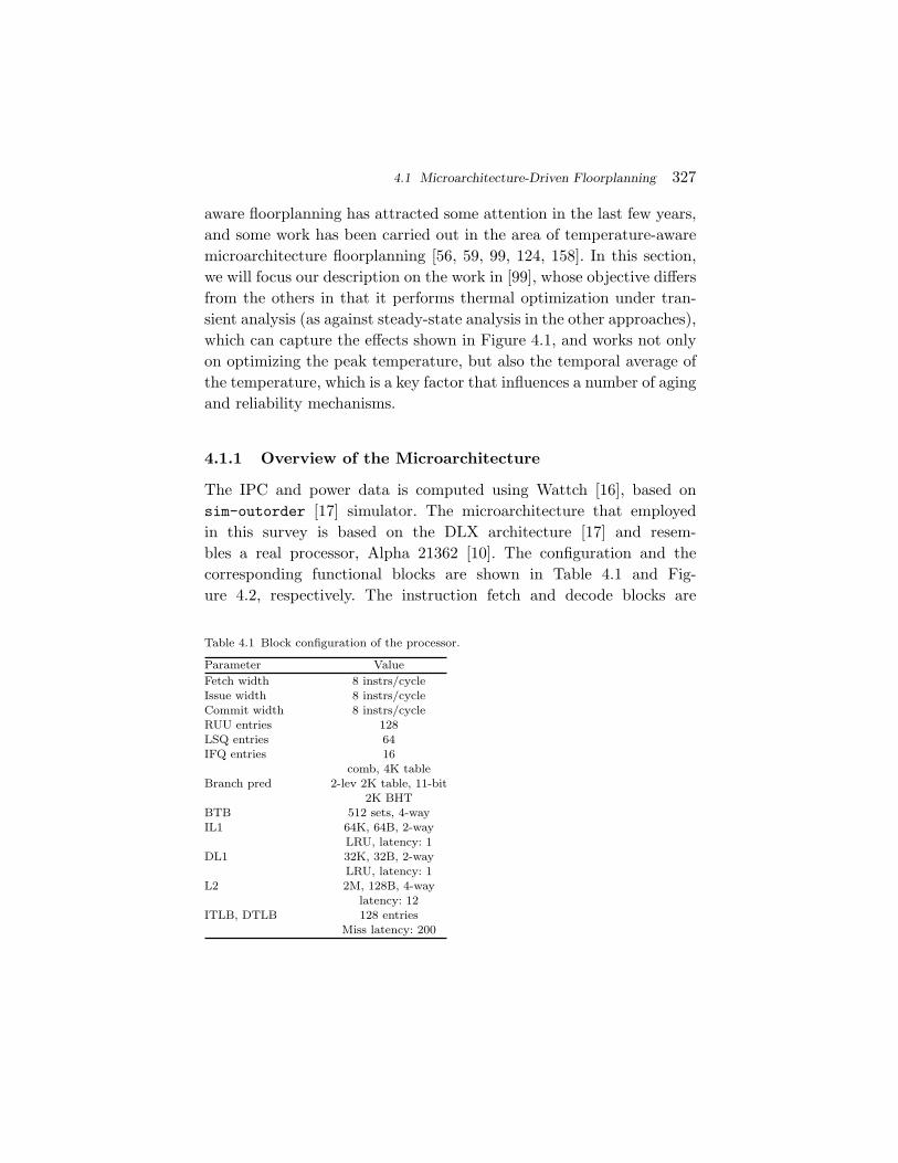
4.1 Microarchitecture-Driven Floorplanning 327
aware floorplanning has attracted some attention in the last few years,and some work has been carried out in the area of temperature-awaremicroarchitecture floorplanning [56, 59, 99, 124, 158]. In this section,we will focus our description on the work in [99], whose objective differsfrom the others in that it performs thermal optimization under tran-sient analysis (as against steady-state analysis in the other approaches),which can capture the effects shown in Figure 4.1, and works not onlyon optimizing the peak temperature, but also the temporal average ofthe temperature, which is a key factor that influences a number of agingand reliability mechanisms.
4.1.1 Overview of the Microarchitecture
The IPC and power data is computed using Wattch [16], based onsim-outorder [17] simulator. The microarchitecture that employedin this survey is based on the DLX architecture [17] and resem-bles a real processor, Alpha 21362 [10]. The configuration and thecorresponding functional blocks are shown in Table 4.1 and Fig-ure 4.2, respectively. The instruction fetch and decode blocks are
Table 4.1 Block configuration of the processor.
Parameter ValueFetch width 8 instrs/cycleIssue width 8 instrs/cycleCommit width 8 instrs/cycleRUU entries 128LSQ entries 64IFQ entries 16
comb, 4K tableBranch pred 2-lev 2K table, 11-bit
2K BHTBTB 512 sets, 4-wayIL1 64K, 64B, 2-way
LRU, latency: 1DL1 32K, 32B, 2-way
LRU, latency: 1L2 2M, 128B, 4-way
latency: 12ITLB, DTLB 128 entries
Miss latency: 200
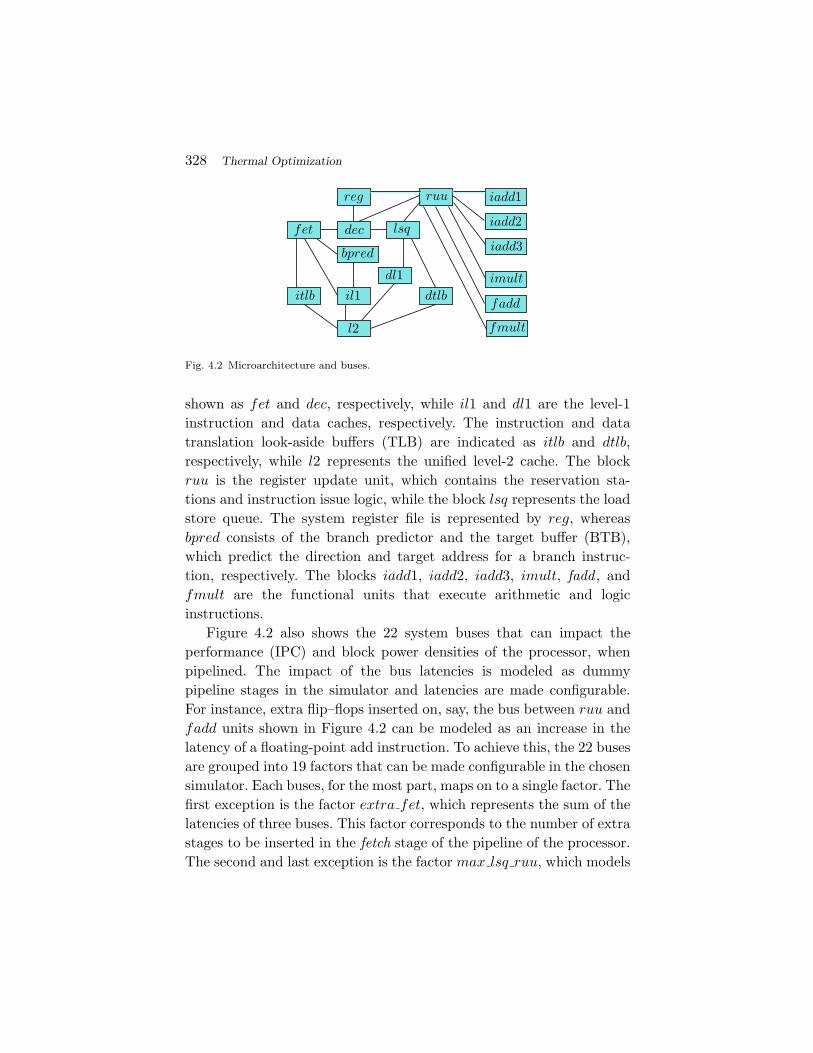
328 Thermal Optimization
Fig. 4.2 Microarchitecture and buses.
shown as fet and dec, respectively, while il1 and dl1 are the level-1instruction and data caches, respectively. The instruction and datatranslation look-aside buffers (TLB) are indicated as itlb and dtlb,respectively, while l2 represents the unified level-2 cache. The blockruu is the register update unit, which contains the reservation sta-tions and instruction issue logic, while the block lsq represents the loadstore queue. The system register file is represented by reg, whereasbpred consists of the branch predictor and the target buffer (BTB),which predict the direction and target address for a branch instruc-tion, respectively. The blocks iadd1, iadd2, iadd3, imult, fadd , andfmult are the functional units that execute arithmetic and logicinstructions.
Figure 4.2 also shows the 22 system buses that can impact theperformance (IPC) and block power densities of the processor, whenpipelined. The impact of the bus latencies is modeled as dummypipeline stages in the simulator and latencies are made configurable.For instance, extra flip–flops inserted on, say, the bus between ruu andfadd units shown in Figure 4.2 can be modeled as an increase in thelatency of a floating-point add instruction. To achieve this, the 22 busesare grouped into 19 factors that can be made configurable in the chosensimulator. Each buses, for the most part, maps on to a single factor. Thefirst exception is the factor extra fet, which represents the sum of thelatencies of three buses. This factor corresponds to the number of extrastages to be inserted in the fetch stage of the pipeline of the processor.The second and last exception is the factor max lsq ruu, which models
4.1 Microarchitecture-Driven Floorplanning 329
the maximum of the latencies of the buses dec ruu and dec lsq. Inter-actions are modeled through additional factors: for example, the busbetween the ruu and fadd units of Figure 4.2 is indicated as ruu fadd
in the table.
4.1.2 Simulation Strategy
The simulations required in this method involve techniques to mea-sure the temperature and the throughput. At the architectural level,this method uses HotSpot [60] for thermal analysis. In HotSpot, thenodes of the multi-layered thermal network are the centers of the blocksof the microarchitecture. HotSpot is used in transient mode, where itaccepts a floorplan, the length of the timestep for transient analysis,and the block power dissipations averaged over each transient timestepas inputs. The heat equation is solved for each timestep to estimatethe new set of temperatures (with the initial conditions being those ofthe previous timestep). The leakage power component of the succeed-ing timestep can then be updated from the new set of temperatures,and the process repeats until the end of the simulation period. Thetimestep for simulation is chosen so that it is sufficiently smaller thanthe thermal time constant of the system, which is of the order of tensof milliseconds.
To measure the throughput, statistical design of experiments, anapproach that characterizes the response of a system in terms ofchanges in the factors which influence the system, is employed. Thebasic idea is to conduct a set of experiments, in which all factors are var-ied systematically over a specified range of acceptable values, such thatthe experiments provide an appropriate sampling of the entire searchspace. The subsequent analysis of the resulting experimental data willidentify the critical factors, the presence of interactions between thefactors, etc. In this survey, the system is a microarchitecture, such asthat shown in Figure 4.2, the response is the IPC/power, and the fac-tors that influence the IPC of the microarchitecture are the latenciesof the buses of the microarchitecture. Since it is impractical to fullyexplore the exponential search space, even when the number of factors(buses) is small (N = 22), a fractional factorial design is employed to

330 Thermal Optimization
reduce the number of simulations. However, such designs are only validwhen some or all of the interactions between the factors are negligible.
The potentially significant interactions that are incorporated intothe DOE framework are shown below:
• Functional unit scheduling: The number of latencies insertedon the three buses between the register update unit and thethree integer adders can be different, and while issuing aninteger add instruction, of all the available units, the onewith the least latency is chosen. This indicates possible sig-nificant (two and three factor) interactions, which need to beestimated.
• Decode stage: The number of extra pipeline stages to beinserted is modeled as a maximum function of three of thelatencies of the buses dec–reg, dec–ruu, and ruu–reg (refer to4.2). Such a nonlinear function can result in significant (twoand three) factor interactions among these three factors.
To control the number of simulations, each factor is restricted tohave two values: the minimum and the maximum possible values forthe factor. The idea is that, by stimulating the system with inputs attheir extreme values, the greatest response is provoked for each input.The assumption is that the system response is a monotone function ofchanges in the inputs (factor levels). Since the factor levels representbus latencies, the extreme (high and low) values can be obtained byassuming worst-case and best-case scenarios for the corresponding wirelengths.
These assumptions allow the use of a 2-level resolution III fractionalfactorial design [94]. For N factors, the number of experiments requiredis equal to the nearest highest power of 2, which turns out to be 32 forour work, since N = 22. We refer the reader to [94] for more details ofthe factorial design methodology.
However, cycle-accurate simulations are inherently slow and mostSPEC benchmarks with reference input sets, when simulated to com-pletion can take days to complete. Therefore, although the resolutionIII design strategy of Section 4.1.2 requires a small number of simula-tions, the run time of each simulation is still an issue. The simulations

4.1 Microarchitecture-Driven Floorplanning 331
are sped up through the use of SMARTS [159], a periodic samplingtechnique, which works well both for throughput (IPC) and power/energy, particularly for the SPEC benchmarks.
The SMARTS technique that is used to speed up the simulationsinvolves fastforwarding program segments between successive sampleschosen for detailed simulation. However, the transient modeling that isused to estimate the thermal metrics requires that the block power den-sities be collected periodically for every timestep. For this, the powerdata collected for each sample is extrapolated for the succeeding fast-forwarded portion.
The total execution time obtained from a simulation is then seg-mented into slots of size equal to the transient analysis timestep. Inother words, the data collected from the simulation can be arranged asan array P indexed by the timestep and the block number, i.e., the entryP (a,b) of the array corresponds to the power consumption of block b
(one of the 17 blocks of Figure 4.2) during timestep a. Since 32 simula-tions are performed (per benchmark), there are 32 such tables. For eachentry P (a,b) (per benchmark), a regression model is constructed fromthe 32 values [94], where the variables are the bus latencies. Equa-tion (4.1) shows one such model, constructed to estimate the powerdissipation at entry P (a,b), where βis represent the regression coeffi-cients computed from the 32 values obtained for the correspond entry(a,b). Each x variable in the model, say xi, represents an encoding ofthe latency of bus i, li, where the minimum and the maximum latenciesare coded as −1 and +1, respectively, and I is the set of interactionterms described above. In other words,
xi = −1 +(
2 · limin(i) + max(i)
), 1 ≤ i ≤ 19
P (a,b) = β0 +19∑i=1
βi · xi +∑
(ij)∈Iβij · xi · xj
+∑
(ijk)∈Iβijk · xi · xj · xk. (4.1)
An IPC regression model is similarly constructed from the statisticsgathered from the 32 simulations for each benchmark.
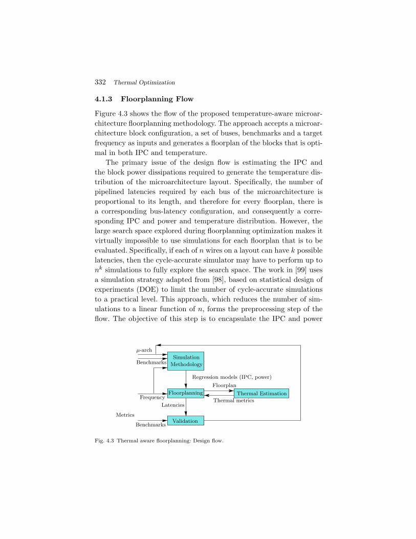
332 Thermal Optimization
4.1.3 Floorplanning Flow
Figure 4.3 shows the flow of the proposed temperature-aware microar-chitecture floorplanning methodology. The approach accepts a microar-chitecture block configuration, a set of buses, benchmarks and a targetfrequency as inputs and generates a floorplan of the blocks that is opti-mal in both IPC and temperature.
The primary issue of the design flow is estimating the IPC andthe block power dissipations required to generate the temperature dis-tribution of the microarchitecture layout. Specifically, the number ofpipelined latencies required by each bus of the microarchitecture isproportional to its length, and therefore for every floorplan, there isa corresponding bus-latency configuration, and consequently a corre-sponding IPC and power and temperature distribution. However, thelarge search space explored during floorplanning optimization makes itvirtually impossible to use simulations for each floorplan that is to beevaluated. Specifically, if each of n wires on a layout can have k possiblelatencies, then the cycle-accurate simulator may have to perform up tonk simulations to fully explore the search space. The work in [99] usesa simulation strategy adapted from [98], based on statistical design ofexperiments (DOE) to limit the number of cycle-accurate simulationsto a practical level. This approach, which reduces the number of sim-ulations to a linear function of n, forms the preprocessing step of theflow. The objective of this step is to encapsulate the IPC and power
Fig. 4.3 Thermal aware floorplanning: Design flow.
4.2 Thermally driven Placement and Routing for 3D Circuits 333
dependence on bus latencies in the form of regression models, whichare used by the floorplanner and the thermal simulator.
The floorplanner is based on a simulated annealing (SA) frameworkand uses the regression models to optimize a cost function, which isa weighted sum of traditional objectives such as the chip area (Area)and the aspect ratio (AR), as well as thermally related cost componentsrelated to the average (Tavg) and the peak (Tpeak) transient tempera-tures, as shown below:
Cost = W1 · Area + W2 · AR + W3 · 1CPI
+ W4 · (Tavg + Tpeak),
(4.2)where the W s represent the relative weights of the optimization terms.
After every SA move, the floorplanner constructs the block powerdensities from the regression models derived in the DOE procedure,and passes the data along with the corresponding layout to the ther-mal simulator, which in turn returns the thermal metrics that are usedin the floorplanning cost function. The performance and thermal pro-file of the resultant layout can then be estimated from cycle-accuratesimulations. In addition, the entire design flow of Figure 4.3 may berepeated for several microarchitectural block configurations to identifythe optimal configuration [31].
The application of this approach shows significant improvementsover methods that are not thermally aware, with peak temperaturereductions of up to about 20%, and average temperature reductions ofup to about 15%.
4.2 Thermally driven Placement and Routing for 3DCircuits
Our second case study on thermally driven optimization operates at alower level of abstraction than the first, and involves the problem ofthermally driven physical design for 3D circuits, which are liable to haveacute thermal problems, as described in Section 1.2.2. Physical designprovides a great deal of flexibility in rearranging the locations of theheat sources, and in improving the conductivity of thermal pathwaysin a circuit.
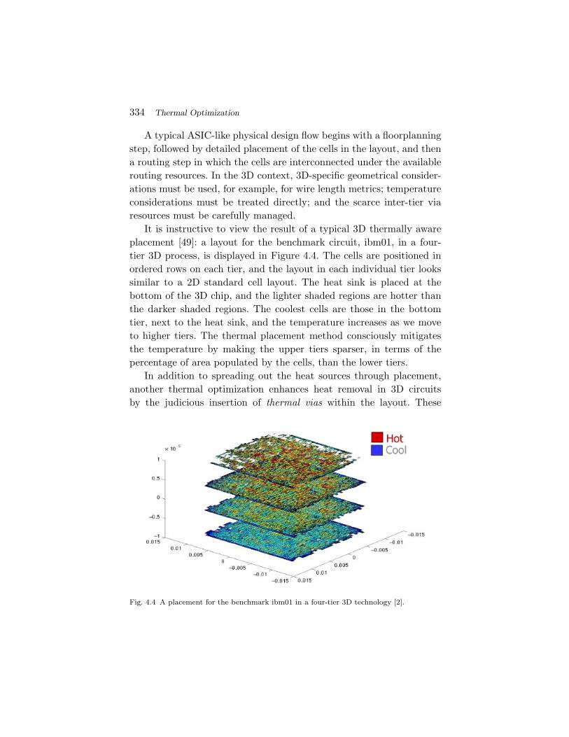
334 Thermal Optimization
A typical ASIC-like physical design flow begins with a floorplanningstep, followed by detailed placement of the cells in the layout, and thena routing step in which the cells are interconnected under the availablerouting resources. In the 3D context, 3D-specific geometrical consider-ations must be used, for example, for wire length metrics; temperatureconsiderations must be treated directly; and the scarce inter-tier viaresources must be carefully managed.
It is instructive to view the result of a typical 3D thermally awareplacement [49]: a layout for the benchmark circuit, ibm01, in a four-tier 3D process, is displayed in Figure 4.4. The cells are positioned inordered rows on each tier, and the layout in each individual tier lookssimilar to a 2D standard cell layout. The heat sink is placed at thebottom of the 3D chip, and the lighter shaded regions are hotter thanthe darker shaded regions. The coolest cells are those in the bottomtier, next to the heat sink, and the temperature increases as we moveto higher tiers. The thermal placement method consciously mitigatesthe temperature by making the upper tiers sparser, in terms of thepercentage of area populated by the cells, than the lower tiers.
In addition to spreading out the heat sources through placement,another thermal optimization enhances heat removal in 3D circuitsby the judicious insertion of thermal vias within the layout. These
Fig. 4.4 A placement for the benchmark ibm01 in a four-tier 3D technology [2].
4.2 Thermally driven Placement and Routing for 3D Circuits 335
vias correspond to inter-tier metal connections that have no electri-cal function, but instead, constitute a passive cooling technology thatdraws heat from the problem areas to the heat sink. Thermal viainsertion can be built into floorplanning, placement and routing, orperformed as an independent post-processing step, depending on thedesign methodology.
4.2.1 Thermal Vias
While silicon is a good thermal conductor, with half or more of the con-ductivity of typical metals, many of the materials used in 3D technolo-gies are strong insulators that place severe restrictions on the amountof heat that can be removed, even under the best placement solution.The materials include epoxy bonding materials used to attach 3D tiers,or field oxide, or the insulator in an SOI technology. Therefore, the useof deliberate metal lines that serve as heat removing channels, called“thermal vias,” are an important ingredient of the total thermal solu-tion. The second step in the flow determines the optimal positions ofthermal vias in the placement that provides an overall improvementin the temperature distribution. In realistic 3D technologies, the foot-prints of these inter-tier vias are of the order of 5µm × 5µm.
In principle, the problem of placing thermal vias can be viewedas one of determining one of two conductivities (corresponding to thepresence or absence of metal) at every candidate point where a thermalvia may be placed in the chip. However, in practice, it is easy to seethat such an approach could lead to an extremely large search spacethat is exponential in the number of possible positions; note that theset of possible positions in itself is extremely large.
Quite apart from the size of the search space, such an approach isunrealistic for several other reasons. First, the wanton addition of ther-mal vias in any arbitrary region of the layout would lead to nightmaresfor a router, which would have to navigate around these blockages. Sec-ond, from a practical standpoint, it is unreasonable to perform full-chipthermal analysis, particularly in the inner loop of an optimizer, at thegranularity of individual thermal vias. At this level of detail, individ-ual elements would have to correspond to the size of a thermal via,

336 Thermal Optimization
and the size of the thermal simulation matrix would become extremelylarge.
Fortunately, there are reasonable ways to overcome each of theseissues. The blockage problem may be controlled by enforcing disciplinewithin the design, designating a specific set of areas within the chip aspotential thermal via sites. These could be chosen as specific inter-rowregions in the cell-based layout, and the optimizer would determine thedensity with which these are filled with thermal vias. The advantage tothe router is obvious, since only these regions are potential blockages,which is much easier to handle. One could work with a two-level schemewith relatively large elements, where the average thermal conductivityof each region is a design variable. Once this average conductivity ischosen, it could be translated back into a precise distribution of thermalvias within the element that achieves that average conductivity.
Various published methods take different approaches to thermal viainsertion. We will now describe an algorithm to post-facto thermal viainsertion [50]; other procedures perform thermal via insertion duringfloorplanning, placement or routing, and will be discussed in the appro-priate sections.
For a given placed 3D circuit, an iterative method was developed in[50] which, during each iteration, the thermal conductivities of certainFEA elements (thermal via regions) are incrementally modified so thatthermal problems are reduced or eliminated. Thermal vias are generi-cally added to elements to achieve the desired thermal conductivities.The goal of this method is to satisfy given thermal requirements usingas few thermal vias as possible, i.e., keeping the thermal conductivitiesas low as possible.
The approach uses the finite element equations to determine a tar-get thermal conductivity. A key observation in this survey is that theinsertion of thermal vias is most useful in areas with a high thermalgradient, rather than areas with a high temperature. Effectively, thethermal via acts as a pipe that allows the heat to be conducted fromthe higher temperature region to the lower temperature region; this, inturn, leads to temperature reductions in areas of high temperature.
This is illustrated in Figure 4.5, which shows the 3D layout ofthe benchmark struct, before and after the addition of thermal vias,

4.2 Thermally driven Placement and Routing for 3D Circuits 337
Fig. 4.5 Thermal profile of struct before (left) and after (right) thermal via insertion. Thetop four layers of the figure at right correspond to the four layers in the figure at left [51].
respectively. The hottest region is the center of the uppermost tier, anda major reason for its elevated temperature is because the tier belowit is hot. Adding thermal vias to remove heat from the second tier,therefore, effectively also significantly reduces the temperature of thetop tier. For this reason, the regions where the insertion of thermal viasis most effective are those that have high thermal gradients.
Therefore the method in [50] employs an iterative update formulaof the type
Knewi = Kold
i
( | goldi |
gi,ideal
)i = x, y, z, (4.3)
where Knewi and Kold
i are, respectively, the old and new thermal con-ductivities in each direction, before and after each iteration, gold
i is theold thermal gradient, and gi,ideal is a heuristically selected ideal thermalgradient.
Each iteration begins with a distribution of the thermal vias; thisdistribution is corrected using the above update formula, and the Knew
i
value is then translated to a thermal via density, and then a preciselayout of thermal vias, using precharacterization. The iterations endwhen the desired temperature profile is achieved. This essential iterative
338 Thermal Optimization
idea has also been used in other methods for thermal via insertion stepsthat are integrated within floorplanning, placement and routing, asdescribed in succeeding sections. This general framework has been usedin several other published techniques that insert thermal vias eitherconcurrently during another optimization, or as an independent step.
4.2.2 3D Floorplanning
The 3D floorplanning problem attempts to find the optimal positions,and possibly, aspect ratios, for a set of large blocks in a layout. Typicalcost functions include a mix of the conventional wirelength and totalarea costs, and the temperature and the number of inter-tier vias.
The approach in [33] presented one of the first approaches to 3Dfloorplanning, and used the TCG representation [85] for each tier, anda bucket structure for the third dimension. Each bucket represents a 2Dregion over all tiers, and stores, for each tier, the indices of the blocksthat intersect that bucket. In other words, the TCG and this bucketstructure can quickly determine any adjacency information. A simu-lated annealing engine is then utilized, with the moves correspondingto perturbations within a tier and across tiers; in each such case, thecorresponding TCG(s) and buckets are updated, as necessary.
A simple thermal analysis procedure is built into this solution, usinga finite difference approximation of the thermal network to build anRC thermal network. Under the assumption that heat flows purelyin the z direction and there is no lateral heat conduction, the RCmodel obtained from a finite difference approximation has a tree struc-ture, and Elmore-delay like computations [125] can be performed todetermine the temperature. The optimization heuristically attemptsto make this a self-fulfilling assumption, by discouraging lateral heatconduction, introducing a cost function parameter that discouragesstrong horizontal gradients. A hybrid approach performs an exact ther-mal analysis once every 20 iterations or so and uses the approximateapproach for the other iterations.
The work in [154] expands the idea of thermally driven floorplan-ning by integrating thermal via insertion into the simulated anneal-ing procedure. A thermal analysis procedure based on random walks

4.2 Thermally driven Placement and Routing for 3D Circuits 339
[115] is built into the method, and an iterative formula, similar to [50],is used in a thermal via insertion step between successive simulatedannealing iterations. The approach in [169] uses a technique based onforce-directed methods for floorplanning, using legalization techniquesto translate the continuous solution to a discrete, layered solution.
4.2.3 3D Placement
In the placement step, the precise positions of cells in a layout aredetermined, and they are arranged in rows within the tiers of the 3Dcircuit. Since thermal considerations are particularly important in 3Dcell-based circuits, this procedure must spread the cells to achieve areasonable temperature distribution, while also capturing traditionalplacement requirements [140].
Several approaches to 3D placement have been proposed in the lit-erature. The work in [38] embeds the netlist hypergraph into the lay-out area. A recursive bipartitioning procedure is used to assign nodesof the hypergraph to partitions, using mincut as the primary objectiveand under partition capacity constraints. Partitioning in the z directioncorresponds to tier assignment, and xy partitions to assigning standardcells to rows. No thermal considerations are taken into account.
The procedure in [49] presents a 3D-specific force-directed placerthat incorporates thermal objectives directly into the placer. Insteadof the finite difference method that is used in many floorplanners, thisapproach employs FEA, as described in Section 2.3.2. The placementengine is based on a force-directed approach: attractive forces are cre-ated between interconnected cells, and weighted together so that theconstants of proportionality are chosen to be higher in the z directionto discourage inter-tier vias; repulsive forces are based on factors suchas the cell overlap and thermal criteria based on the temperature gra-dient. An equilibrium point is found where these forces balance eachother.
Once the entire system of attractive and repulsive forces is gener-ated, repulsive forces are added, the system is solved for the minimumenergy state, i.e., the equilibrium location. Ideally, this minimizes thewire lengths while at the same time satisfying the other design criteria

340 Thermal Optimization
such as the temperature distribution. The iterative force-directedapproach follows the following steps in the main loop. Initially, forcesare updated based on the previous placement. Using these new forces,the cell positions are then calculated. These two steps of calculatingforces and finding cell positions are repeated until the exit criteria aresatisfied. The specifics of the force-directed approach to thermal place-ment, including the mathematical details, are presented in [49]. Oncethe iterations converge, a final postprocessing step is used to legalize theplacement. Even though forces have been added to discourage overlaps,the force-directed engine solves the problem in the continuous domain,and the task of legalization is to align cells to tiers, and to rows withineach tier.
Another method in [32] maps an existing 2D placement to a 3Dplacement through transformations based on dividing the layout into 2k
regions, for integer values of k, and then defining local transformationsto heuristically refine the layout.
More recent work in [52] observes that since 3D layouts have verylimited flexibility in the third dimension (with a small number of lay-ers and a fixed set of discrete locations), partitioning works betterthan a force-directed method. Accordingly, this work performs globalplacement using recursive bisectioning. Thermal effects are incorpo-rated through thermal resistance reduction nets, which are attractiveforces that induce high power nets to remain close to the heat sink.The global placement step is followed by coarse legalization, in whicha novel cell-shifting approach is proposed. This generalizes the meth-ods in FastPlace [147] by allowing shift moves to adjust the boundariesof both sparsely and densely populated cells using a computationallysimple method. Finally, detailed legalization generates a final nonover-lapping layout. The approach is shown to provide excellent tradeoffsbetween parameters such as the number of interlayer vias, wire length,temperature.
4.2.4 Routing Algorithms
During routing, several objectives and constraints must be taken intoconsideration, including avoiding blockages due to areas occupied by

4.2 Thermally driven Placement and Routing for 3D Circuits 341
thermal vias, incorporating the effect of temperature on the delaysof the routed wires, and of course, traditional objectives such as wirelength, timing, congestion, and routing completion. In the 2D arena,results on thermally aware routing have been reported, for example,in [3, 4].
In the 3D context, once the cells have been placed and the locationsof the thermal vias determined, the routing stage finds the optimalinterconnections between the wires. As in 2D routing, it is importantto optimize the wire length, the delay, and the congestion. In addition,several 3D-specific issues come into play. First, the delay of a wireincreases with its temperature, so that more critical wires should avoidthe hottest regions, as far as possible. Second, inter-tier vias are avaluable resource that must be optimally allocated among the nets.Third, congestion management and blockage avoidance is more complexwith the addition of a third dimension. For instance, a signal via orthermal via that spans two or more tiers constitutes a blockage thatwires must navigate around.
Consider the problem of routing in a three-tier technology, as illus-trated in Figure 4.6. The layout is gridded into rectangular tiles, eachwith a horizontal and vertical capacity that determines the numberof wires that can traverse the tile, and an inter-tier via capacity thatdetermines the number of free vias available in that tile. These capaci-ties account for the resources allocated for nonsignal wires (e.g., powerand clock wires) as well as the resources used by thermal vias. For asingle net, as shown in the figure, the degrees of freedom that are avail-able are in choosing the locations of the inter-tier vias, and selecting
Fig. 4.6 An example route for a net in a three-tier 3D technology [2].

342 Thermal Optimization
the precise routes within each tier. The locations of inter-tier vias willdepend on the resource contention for vias within each grid. Moreover,critical wires should avoid the high-temperature tiles, as far as possible.
The work in [35] presents a thermally conscious router, using amultilevel routing paradigm similar to [30, 34], with integrated inter-tier via planning and incorporating thermal considerations. An initialrouting solution is constructed by building a 3D minimum spanningtree (MST) for each multipin net, and using maze routing to avoidobstacles.
At each level of the multilevel scheme, the inter-tier via planningproblem assigns vias in a given region at level k − 1 of the multilevelhierarchy to tiles at level k. The problem is formulated as a min-costmaxflow problem, which has the form of a transportation problem. Theflow graph is constructed as follows:
• The source node of the flow graph is connected throughdirected edges to a set of nodes vi, representing candidatethermal vias; the edges have capacity 1 and cost 0.
• Directed edges connect a second set of nodes, Tj , from eachtile to the sink node, with capacity equaling the number ofvias that the tile can contain, and cost zero. The capac-ity is computed using a heuristic approach that takes intoaccount the temperature difference between the tile and theone directly in the tier below it (under the assumption thatheat flows downwards toward the sink); the thermal analysisis based on a commercial FEA solver.
• The source and sink both have cost m, which equals thenumber of inter-tier vias in the entire region.
• Finally, a node vi is connected to a tile Tj through an arc withinfinite capacity and cost equaling the estimated wirelengthof assigning an inter-tier via vi to tile Tj .
Another approach to 3D routing, presented in [168], combines theproblem of 3D routing with heat removal by inserting thermal vias inthe z direction, and introduces the concept of thermal wires. Like athermal via, a thermal wire is a dummy object: it has no electrical

4.2 Thermally driven Placement and Routing for 3D Circuits 343
a grid cell atthe corner
routing grid
routing graph
vertex inrouting graph
a verticalrouting edge
a grid cellboundary
Fig. 4.7 Routing grid and routing graph for a four-tier 3D circuit [168].
function, but is used to spread heat in the lateral direction. Each tieris tiled into a set of regions, as shown in Figure 4.7.
The global routing scheme goes through two phases. In Phase I,an initial routing solution is constructed. A 3D MST is built for eachmultipin net, and based on the corresponding two-pin decomposition,the routing congestion is statistically estimated over each lateral rout-ing edge using the method in [153]. This congestion model is extendedto 3D by assuming that a two-pin net with pins on different tiers hasan equal probability of utilizing any inter-tier via position within thebounding box defined by the pins.
A recursive bipartitioning scheme is then used to assign inter-tiervias. This is also formulated as a transportation problem, but the for-mulation is different from the multilevel method described above. Signalinter-tier via assignment is then performed across the cut in each recur-sive bipartition. Figure 4.8(a) shows an example of signal inter-tier viaassignment for a decomposed two-pin signal net in a four-tier circuitwith two levels of hierarchy. The signal inter-tier via assignment is firstperformed at the boundary between regions of group 0 and group 1 attopmost level, and then it is processed for tier boundary within eachgroup. At each level of the hierarchy, the problem of signal inter-tiervia assignment is formulated as a min-cost network flow.

344 Thermal Optimization
(a) (b)
assignsignalviasfirst
assignsignal vias
afterhigher-levelassignment
layer 0
layer 1
layer 2
layer 3
group 0
group 1
(capacity, cost) pair
N1
N0
N4
N3
N2
C0
C3
C2
C1S T
(1, 0)(1, cost(N i, Cj)) (Uj, 0)
Fig. 4.8 (a) Example of hierarchical signal via assignment for a four-tier circuit. (b) Exampleof min-cost network flow heuristics to solve signal via assignment problem at each level ofhierarchy [168].
Figure 4.8(b) shows the network flow graph for assigning signalinter-tier vias of five inter-tier nets to four possible inter-tier via posi-tions. The idea is to assign each net that crosses the cut to an inter-tiervia. Each inter-tier net is represented by a node Ni in the network flowgraph; each possible inter-tier via position is indicated by a node Cj .If Cj is within the bounding box of the two-pin inter-tier net Ni, webuild a directed edge from Ni to Cj , and set the capacity to be 1, thecost of the edge to be cost(Ni,Cj). The cost(Ni,Cj) is evaluated asthe shortest path cost for assigning inter-tier via position Cj to net Ni
when both pins of Ni are on the two neighboring tiers; otherwise it isevaluated as the average shortest path cost over all possible unassignedsignal inter-tier via positions in lower levels of the hierarchy. The short-est path cost is obtained with Dijkstra’s algorithm in the 2D congestionmap generated from the previous estimation step, and the cost func-tion for crossing a lateral routing edge is a combination of edge lengthand an overflow cost function similar to that in [55]. The supply at thesource, equaling the demand at the sinks, is N , the number of nets.
Finally, once the inter-tier vias are fixed, the problem reduces toa 2D routing problem in each tier, and maze routing is used to routethe design.
Next, in Phase II, a linear programming approach is used to assignthermal vias and thermal wires. A thermal analysis is performed, and

4.3 Recovering from Runtime Shifts 345
fast sensitivity analysis is carried out using the adjoint network method,which has the cost of a single thermal simulation. The benefit of addingthermal vias, for relatively small perturbations in the via density, isgiven by a product of the sensitivity and the via density, a linear func-tion. The objective function is a sum of via densities and is also linear.Additional constraints are added in the formulation to permit overflows,and a sequence of linear programs is solved to arrive at the solution.
4.3 Recovering from Runtime Shifts
In this section, we will discuss examples of techniques that can be usedto recover from the degradation caused by thermal effects. Specifically,we will begin with a description of methods that use adaptive bodybiases to recover performance and leakage power, then overview adap-tive supply voltage based methods, and finally, discuss thermal guard-banding methods to overcome aging effects, using NBTI degradationas an example. The adaptive techniques, in particular, are examplesof methods that can dynamically change the behavior of the circuitbased on information provided by on-chip sensors. On the other hand,guardbanding methods are purely static design-time approaches thatare used to build sufficient margins to ensure that the circuit functionscorrectly in the presence of stress.
4.3.1 Using Adaptive Body Biases
4.3.1.1 Overview
The fourth terminal of a transistor, after the source, drain and gate, isthe body, and it is typically tied to ground for an NMOS device andthe supply for a PMOS device. Body biasing alters the voltage on thisterminal to achieve threshold voltage modulation, providing an effectiveknob to alter the delay and leakage of the circuit. Typically, the body ofeach transistor is tied to its corresponding well (or substrate), implyingthat the same altered body bias must be applied to all transistors thatshare the well.
Traditionally, this method has been used in two different opera-tional scenarios [93]. The first method, known as static body biasing
346 Thermal Optimization
uses reverse body biasing when the microprocessor is in a stand-bystate, with the aim of reducing the subthreshold leakage current. Algo-rithms to determine the optimal configuration that achieves the low-est leakage in the presence of latency constraints, have been describedin [8, 90, 160, 161, 162]. Such schemes have been used in low powerand embedded systems, where leakage power minimization is the mainobjective. The second scheme, known as adaptive body bias (ABB),involves recovering dies impacted by process variations through post-silicon tuning. Adaptive body bias is a dynamic control technique, usedto tighten the distribution of the maximum operational frequency andthe maximum leakage power, in the presence of within-die (WID) ther-mal or process variations. It was proposed in [152] and was furtherexplored [80] during the design of a DSP processor. The main goal ofthis scheme is to ensure that maximum number of dies operate in thehighest frequency bin, thereby increasing the yield of the fabricationprocess [141, 142].
Bidirectional adaptive body bias has been shown to reduce theimpact of D2D and WID parameter variations on microprocessor fre-quency and leakage in [25, 141, 142, 144, 145]. Typically, devices thatare slow but do not leak too much can be Forward Body Biased (FBB)to improve the speed, whereas devices that are fast and leaky can beReverse Body Biased (RBB) to meet the leakage budget. The work in[97, 142] performs process variation-based ABB, and divides the dieinto a set of WID-variational regions. In each region, test structuresthat are replicas of the critical path, are built. The delay and leakagevalues of these test structures are measured, and are used to deter-mine the exact body bias values that are required to counter processvariations at room temperature. The application of a WID–ABB tech-nique for one-time compensation during the test phase, in [142], showsthat 100% of the dies can be salvaged, while 99% of them operate atfrequencies within the fastest bin.
4.3.1.2 Implementing ABB
If the foundry is capable of supporting a triple well process, the N-well(s) and the P-well(s) can be independently biased. Techniques for

4.3 Recovering from Runtime Shifts 347
clustering gates, into wells that can be separately biased, are presentedin [76]. The body bias to be applied is denoted by the tuple, (vbn,vbp)where in general, each element of the tuple can be a vector, correspond-ing to wells that can be separately biased. Note that the actual volt-age applied to the body of the PMOS transistors is (Vdd − vbp), whereVdd is the supply voltage. The range of operating temperatures, andthe extent of process variations, over which thermal variations can becompensated for, each depends on the minimum and maximum limitsimposed on the body bias voltages, due to device physics restrictions.It is important to note that if the applied body bias is too large, it mayexceed the cut-in voltage of p–n junctions associated with the structureof a transistor. Additionally, the maximum amount of body bias is alsoconstrained by the permissible leakage budget of the circuit block, sinceFBB reduces the delay at the expense of an increase in the leakage. Theexact resolution of bias voltages is primarily determined by constraintson generating and routing these voltages to every biasable well in thecircuit.
The control mechanism necessary to ensure that the requisite volt-ages are selected can either be built using a critical path replica basedcontrol system or a look-up table based control system. The hardwareon-chip control set-up, as built in [93, 142], requires a test structurethat replicates the critical path (assuming there is only one such path),which is expected to accurately reflect the behavior of the entire cir-cuit, and the impact on delay and leakage due to on-chip variations. Thecontrol circuit consists of a delay monitor, phase comparator, decoder,digital–analog converter (DAC), and such other precision hardware toautomatically select the bias pair, (vbn,vbp). Although such schemesare self-adapting, and require minimal post-silicon testing, a few sam-ple critical path replicas might be unable to reflect the exact nature ofprocess and thermal variations on the actual circuit, which consists ofmillions of paths. Experimental results in [142] indicate that a minimumof 14 critical path replicas per test-chip are required to accurately deter-mine the die frequency of microprocessors, for a 130 nm based process.The increased impact of process variations in sub-100 nm technologiesis likely to require a larger number of critical path replicas to be fabri-cated per test-chip to ensure a high level of confidence in the frequency
348 Thermal Optimization
measurements for a 65 nm or a 45 nm based design. This may lead toa substantial area overhead. Further, if the test circuits are large, theymeasure their own variations, which may not be the same as that ofthe actual circuit. Thus, the additional area overhead imposed by thenumber of critical path replicas and their inaccuracies, coupled with theneed for PVT (process, voltage, and temperature) invariant hardware,call for better control mechanisms.
A viable alternative to the critical path replica based control systemis the look-up table based control system. In this case, every block isequipped with a look-up table [93, 101] that can store the bias values(vbn,vbp). These are the precomputed optimal values that can com-pensate for thermal and process parametric variations. Each entry inthe look-up table corresponds to a different temperature point. Theseentries are calibrated off-line through post-silicon measurements, withthe aid of an efficient algorithm, i.e., using software. The look-up tableis assumed to be built using a simple ROM like structure, and is popu-lated during post-silicon testing. When the circuit is in operation, theentries in the look-up table are keyed based on the operating tempera-ture, which is measured by a temperature sensor, as shown in [101]. Theoutput of the table is fed to the body bias network to generate and routethe appropriate voltages, thereby providing run-time compensation.
The look-up table based control system eliminates the various issuesassociated with using critical path replicas as test structures, to capturethe effect of process and thermal variations, on the entire chip. Sincethe body bias voltages are already precomputed, they may be immedi-ately applied to the entire chip, to compensate for on-chip temperaturevariations, without affecting the run-time operation. An overall archi-tectural implementation of this control scheme is explained in the nextsubsection.
Further, the effect of voltage variations, as well as aging, can beincorporated by adding appropriate sensors, and introducing an addi-tional entry, i.e., supply voltage (Vdd), along with vbn and vbp, tothe look-up table. The algorithms can be modified accordingly,to determine the optimal body bias and supply voltage configura-tion, to overcome the effects of process and thermal variations, and

4.3 Recovering from Runtime Shifts 349
Fig. 4.9 A generic ABB implementation architecture showing the structure of the WID-variational regions.
temporal degradation. A practical example of a system that uses theabove scheme, and compensates for PVT variations, as well as aging,is seen in a 90 nm-based design in [143].
An implementation for the look-up table control scheme based bodybias compensation network is shown in Figure 4.9. The chip is parti-tioned into several WID-variational regions, each of which must be com-pensated independently. The implementation assumes a central bodybias network capable of generating the requisite voltage to each block.Alternatively, each block may have its own body bias generation anddistribution network. Each WID-variational region is equipped with atemperature sensor that is capable of tracking variations in on-chipoperating temperature. The temperature sensor references a ROM,that stores the (vbn, vbp) values for each compensating temperature,in the form of a look-up table. The output of the look-up table feedsthe central (or local) body bias generator, and accordingly generatesthe required voltages. These voltages are then routed to the correspond-ing N and P wells. The NMOS and PMOS body bias voltages may beapplied by external sources during testing. Once the final voltages aredetermined, and the look-up table has been populated, the switchescan be closed and the requisite voltages required for compensation aresupplied from the on-chip body bias generation network.

350 Thermal Optimization
4.3.1.3 Using ABB for Thermal Compensation
ABB has been used to compensate for process [142, 144, 145] as well astemperature [78, 101] variations. The work in [78] applies a combinationof temperature-based ABB, and a process-based ABB to permit thecircuit to recover from changes due to both temperature and processvariations. In order to be able to adaptively body bias the dies atall operating temperatures, an efficient self-adjusting mechanism isemployed, which can sense the operating temperature, and therebydynamically regulate the voltages that must be applied to the body ofthe devices to meet the performance constraints.
Computational techniques for efficiently determining the exactamount of bias required to achieve process and temperature compen-sation, to populate the look-up table such that the time spent on thetester is minimized, are proposed in [78]. Two methods for comput-ing the final body bias values are proposed: the PTABB (Process andTemperature Adaptive Body Bias) algorithm and the PABB–TABB(Process Adaptive Body Bias–Temperature Adaptive Body Bias) algo-rithm. Both methods use mathematical models to express the delay andleakage as functions of the NMOS and the PMOS transistor body biasvoltages. A two variable nonlinear optimization problem is formulatedand an optimizer is used to determine the configuration that meets thedelay requirement, and thereby minimizes the overall leakage.
While the PTABB algorithm involves measuring the delay andleakage at sample points for each individual die or WID-variationalregion, at each compensating temperature, the PABB–TABB algo-rithm involves measurements only at the nominal operating tempera-ture. The PABB–TABB algorithm splits the original problem into twosub-problems, namely compensating for process variations at nominaltemperature (PABB), and compensating for thermal variations underideal process conditions (TABB). The final set of bias voltages is sim-ply a combination of the PABB and TABB voltages. Thus, this schememinimizes the number of tester measurements, and eliminates the needto test at each operating temperature. Experimental results on a 65 nmand a 45 nm technology demonstrate the ability of the PTABB and thePABB–TABB algorithms to closely predict the body bias voltages.

4.3 Recovering from Runtime Shifts 351
4.3.2 Using Adaptive Supply Voltages and Frequencies
As in the case of body biases, adaptive supply voltages can be usedto recover performance in the presence of thermal variations. The keyobservation here is that elevated temperatures are caused by increasedpower dissipation, and the quadratic dependence between the dynamicpower and the supply voltage, Vdd, implies that changing the value ofVdd is an effective knob for controlling on-chip thermal effects. Similarly,slowing down the processor by reducing the chip frequency also pro-vides reductions in the power dissipation, and hence the temperature.Cumulatively, scaling both the supply voltage and frequency allows apotentially cubic reduction in power.
The idea of throttling the processor was proposed in [123] for aPowerPC processor by adaptively altering its frequency, based on feed-back from a thermal assist unit (TAU) that monitors junction temper-atures of devices on the chip, using a temperature sensor that uses adifferential scheme, based on the voltage across a pair of diodes. TheTAU compares the temperature against one or two user-programmedthresholds, and generates a thermal management interrupt if thethreshold is exceeded. The approaches in [24, 144] show how sensor-based approaches may be used to provide adaptive feedback to alterthe supply voltage in response to thermal changes. A control-theoreticframework for this purpose is described in [133], where a simple pro-portional controller is used to update the supply voltage.
Voltage and frequency scaling techniques have also been incorpo-rated into the design of an Itanium-family processor, codenamed theMontecito, as described in [44, 92, 107], and illustrated in Figure 4.10.Four on-die thermal sensors are used, and are sampled at low frequen-cies (with periods of the order of 20 ms). The voltage regulator providesthree possible supply voltages to the processor, one to the core, one tothe cache, and a fixed, nonvarying voltage for special circuitry. Theclosed loop thermal management control system senses the dissipatedpower, and generates an error signal that shows the difference betweenthe actual power and the power limit. This signal goes through aninfinite impulse response (IIR) filter, and then to saturating modulesthat ensure that the supply voltage remains with the desired range of

352 Thermal Optimization
Fig. 4.10 Control system for a 90 nm Itanium processor, taking in inputs from thermalsensors, and adaptively changing the processor supply voltage and frequency [92].
0.9–1.25 V, and generates a signal that determines the voltage to begenerated by the regulator. The variable frequency clock system reactsto changes in the voltage and adapts the frequency to be appropri-ate for the applied voltage. The control system is designed to have atransient response of 250µs.
An approach to solving this problem for embedded applications waspresented in [167]. Since the functionalities for embedded applicationsare well characterized, it is possible to perform static scheduling atdesign time in this domain. The work assumes a periodic sequenceof tasks to be scheduled, and uses a polynomial-time approximationalgorithm to solve an offline dynamic voltage and frequency scaling(DVFS) formulation.
4.3.3 NBTI Guardbanding
The physical explanations for the NBTI mechanism, which correspondto various models [5, 6, 7, 12, 19, 77, 146], are unanimous in agreeingthat the PMOS transistor threshold voltage rises logarithmically withtime. This rise could lead to an increase of up to 25%–30% in the valueof the threshold voltage after 10 years, depending on the process. Theextent of threshold voltage degradation is strongly dependent on theamount of time for which the device has been stressed and relaxed,
4.3 Recovering from Runtime Shifts 353
since the generation of traps under negative bias stress is followed byannealing of the traps during recovery, (i.e., when the stress is relaxed).Circuit simulations using these models have shown that NBTI causesthe delay of digital circuits to worsen by about 10% [77, 105, 106].
A general solution to maintaining optimal performance under theinfluence of NBTI has been to reduce the delay of the critical pathsthrough the use of gate sizing [106, 146]. The work in [106] formulatesa nonlinear optimization problem to determine the optimal set of gatesizes required to ensure that the circuit runs at its delay specification,after 10 years of operation. The work is based on a model for NBTI,that ignores the effect of recovery, in computing the threshold voltagedegradation. The model cumulatively adds the time for which the gatesare stressed during their entire lifetime, and estimates the thresholdvoltage degradation, assuming that the gates are continuously stressedfor that duration. Hence, their results show that the increase in thecircuit area is rather weakly dependent on the signal probabilities ofthe nodes, and assuming that all gates in the circuit are always NBTIaffected (worst case design) does not significantly affect the final solu-tion. The authors consider the gate sizes to be continuous, and showthat an increase in area of about 8.7%, as compared to a design thatignores NBTI effects, is required to meet the target delay.
The above idea can be readily used in other transforms, such astechnology mapping, by replacing the nominal value of the delays of thegates in the standard cell library, with the delay under worst case NBTI.The target frequency is given to the synthesis tool, and technologymapping can be performed using these NBTI-affected library cells toproduce a circuit, which is structurally different from that obtainedusing the sizing algorithm in [106], but is functionally equivalent, andmeets the timing requirement.
However, the worst-case assumption that ignores the effect of signalprobabilities on the delay can be pessimistic, since the annealing orhealing process on the removal of NBTI stress can partially reverse thethreshold voltage degradation due to NBTI. This happens frequentlyin a circuit: for example, when the input signal to a CMOS inverterchanges from logic 0 to logic 1, the Vgs stress is relaxed from −Vdd
to zero. The recovery in threshold voltage on removing the applied

354 Thermal Optimization
stress, can be explained by physical mechanisms related to annealingof interface traps, and reformation of Si–H bonds. Experiments in [5,19], and subsequently the models in [12, 77, 146], have shown thatconsidering the effect of annealing and recovery has a significant bearingon the overall NBTI impact.
The work in [79] considers the effect of NBTI, including recoveryeffects, during the technology mapping process. Since a digital circuitconsists of millions of nodes with differing signal probabilities, it isessential to estimate the delay of the gates in the library based ontheir input node signal probabilities, and use these delay values duringtechnology mapping. The mapping process can be used to “hide” highprobability nodes within a gate, and reduce the potential for NBTIdegradation. The essential idea of the approach is to modify the processof technology mapping, using the signal probability (defined as theprobability that the signal is low), denoted by SP, of the nodes in thecircuit. The SP values of the primary inputs are determined, basedon RTL-level simulations and statistical estimates. The SP values atevery other node in the subject graph are calculated accordingly, andthis information is used to choose the best gate to meet the timing ateach node. Experimental results indicate that an average 10% recoveryin area can be obtained using the SP-based method, as opposed to theworst case NBTI based method.

5Conclusion
The objective of this survey has been to provide a meaningful overviewof techniques for thermal analysis and electrothermal optimization. Itshould be noted that the predecessors of the work described herein liein early work on transistor level thermal simulation, thermal simulationof microwave ICs, package-level simulation, etc., but to maintain thefocus of this survey, we have restricted our descriptions to the on-chipcontext.
Techniques for on-chip simulation are now available at varying lev-els of accuracy and computational efficiency, as described in the chap-ter on Thermal Analysis Optimizations. These may apply to thermalsimulation and optimization in much the same way that circuit simu-lators or analyzers are used: the more accurate and detailed versionsare employed in verification, while the more approximate approachesare adequate for optimization, as long as they show sufficient fidelity.Electrothermal analysis techniques, which closely couple thermal anal-ysis with circuit performance, are extremely useful in on-chip thermaloptimization. These methods must include mechanisms that ensure self-consistency, so that the impact of electrical effects on thermal effects,and vice versa, are taken into consideration.
355
356 Conclusion
Finally, thermal optimization and mitigation form a key part ofany thermally conscious design strategy. To the extent possible, it isdesirable to control the on-chip temperature and prevent it from rising,in order to control both near-term degradations in performance metricssuch as power and delay, due to elevated temperatures, as well as long-term reliability-related problems. At the point where temperature levelscan no longer be controlled, or where control comes at an unacceptablecost, it is essential to mitigate any effects through adaptive approaches,or through guardbanding.
Acknowledgments
The authors gratefully acknowledge the role of their past collaborationswith (alphabetically) Charlie Chung-Ping Chen, Brent Goplen, DavidJ. Lilja, Sani R. Nassif, Vidyasagar Nookala, Haifeng Qian, and TianpeiZhang.
357
References
[1] “HotSpot,” available at: http://lava.cs.virginia.edu/HotSpot/index.htm.[2] C. Ababei, Y. Feng, B. Goplen, H. Mogal, T. Zhang, K. Bazargan, and S. Sap-
atnekar, “Placement and routing in 3D integrated circuits,” IEEE Design andTest, vol. 22, no. 6, pp. 520–531, November–December 2005.
[3] A. H. Ajami, K. Banerjee, and M. Pedram, “Analysis of substrate thermalgradient effects on optimal buffer insertion,” in Proceedings of the IEEE/ACMInternational Conference on Computer-Aided Design, pp. 44–48, 2001.
[4] A. H. Ajami, K. Banerjee, and M. Pedram, “Modeling and analysis of nonuni-form substrate temperature effects on global ULSI interconnects,” IEEETransactions on Computer-Aided Design of Integrated, vol. 24, no. 6, pp. 849–861, June 2005.
[5] M. A. Alam, “A critical examination of the mechanics of dynamic NBTI forpMOSFETs,” in IEEE International Electronic Devices Meeting, pp. 14.4.1–14.4.4, 2003.
[6] M. A. Alam, “On the reliability of micro-electronic devices: An introductorylecture on negative bias temperature instability,” Nanotechnology 501 LectureSeries; available at http://www.nanohub.org/resources/?id=193, 2005.
[7] M. A. Alam and S. Mahapatra, “A comprehensive model of PMOS NBTIdegradation,” Journal of Microelectronics Reliability, vol. 45, pp. 71–81,August 2004.
[8] A. Andrei, M. Schmitz, P. Eles, Z. Peng, and B. M. Al-Hashimi, “Overhead-conscious voltage selection for dynamic and leakage energy reduction of time-constrained systems,” in Proceedings of the Design, Automation and Test inEurope, pp. 518–523, 2004.
358

References 359
[9] K. Banerjee and A. Mehrotra, “Global (interconnect) warming,” IEEE Cir-cuits and Devices, pp. 16–32, September 2001.
[10] P. Bannon, “Alpha 21364: A scalable single-chip SMP,” available at:http://www.digital.com/alphaoem/micro- processorforum.htm, 1998.
[11] W. Batty, C. E. Christoffersen, A. J. Panks, S. David, C. M. Snowden, andM. B. Steer, “Electrothermal CAD of power devices and circuits with fullyphysical time-dependent compact thermal modeling of complex nonlinear 3-Dsystems,” IEEE Transactions on Components and Packaging Technologies,vol. 34, no. 4, pp. 566–590, December 2001.
[12] S. Bhardwaj, W. Wang, R. Vattikonda, Y. Cao, and S. Vrudhula, “Predictivemodeling of the NBTI effect for reliable design,” in Proceedings of the IEEECustom Integrated Circuits Conference, pp. 189–192, 2006.
[13] J. R. Black, “Electromigration failure modes in aluminum metallization forsemiconductor devices,” in Proceedings of the IEEE, vol. 57, pp. 1587–1594,September 1969.
[14] K. Bowman, L. Wang, X. Tang, and J. Meindl, “A circuit-level perspective ofthe optimum gate oxide thickness,” IEEE Transactions on Electron Devices,vol. 48, no. 8, pp. 1800–1810, August 2001.
[15] W. L. Briggs, “A multigrid tutorial,” http://www.llnl.gov/CASC/people/henson/mgtut/ps/mgtut.pdf.
[16] D. Brooks, V. Tiwari, and M. Martonosi, “Wattch: A framework forarchitectural-level power analysis and optimization,” in Proceedings of theACM International Symposium on Computer Architecture, pp. 83–94, 2000.
[17] D. C. Burger and T. M. Austin, “The SimpleScalar tool set, version 2.0,” Tech-nical Report CS-TR-97-1342, The University of Wisconsin, Madison, June1997.
[18] J. Burns, L. McIlrath, J. Hopwood, C. Keast, D. P. Vu, K.Warner, andP. Wyatt, “An SOI-based three dimensional integrated circuit technology,”in Proceedings of the IEEE International SOI Conference, pp. 20–21, 2000.
[19] S. Chakravarthi, A. T. Krishnan, V. Reddy, C. Machala, and S. Krishnan, “Acomprehensive framework for predictive modeling of negative bias tempera-ture instability,” in Proceedings of the IEEE International Reliability PhysicsSymposium, pp. 273–282, 2004.
[20] H. Chang and S. S. Sapatnekar, “Prediction of leakage power under processuncertainties,” in Proceedings of the ACM Transactions on Design Automationof Electronic Systems, vol. 12, no. 2, April 2007.
[21] G. Chen, K. Y. Chuah, M. F. Li, D. S. H. Chan, C. H. Ang, J. Z. Cheng, Y. Jin,and D. L. Kwong, “Dynamic NBTI of PMOS transistors and its impact ondevice lifetime,” in Proceedings of the IEEE International Reliability PhysicsSymposium, pp. 196–200, 2003.
[22] G. Chen, M. F. Li, C. H. Ang, J. Z. Zheng, and D. L. Kwong, “Dynamic NBTIof p-MOS transistors and its impact on MOSFET scaling,” in Proceedings ofthe IEEE International Reliability Physics Symposium, pp. 196–202, 2003.
[23] G. Chen and S. S. Sapatnekar, “Partition-driven standard cell placement,” inProceedings of the International Symposium on Physical Design, pp. 75–80,2003.

360 References
[24] Q. Chen, M. Meterelliyoz, and K. Roy, “A CMOS thermal sensor and its appli-cations in temperature adaptive design,” in Proceedings of the IEEE Interna-tional Symposium on Quality Electronic Design, 2006.
[25] T. Chen and S. Naffziger, “Comparison of adaptive body bias (ABB) andadaptive supply voltage (ASV) for improving delay and leakage under thepresence of process variation,” IEEE Transactions on VLSI Systems, vol. 11,no. 5, pp. 888–899, October 2003.
[26] T.-Y. Chiang, K. Banerjee, and K. C. Saraswat, “Analytical thermal model formultilevel VLSI interconnects incorporating via effect,” IEEE Electron DeviceLetters, vol. 23, no. 1, pp. 31–33, January 2002.
[27] R. C. Chu, R. E. Simons, and G. M. Chrysler, “Experimental investigation ofan enhanced thermosyphon heat loop for cooling a high performance electron-ics module,” in Proceedings of the IEEE Semiconductor Thermal Measurementand Management Symposium (Semitherm), pp. 1–9, 1999.
[28] L. O. Chua and P.-M. Lin, Computed-Aided Analysis of Electronic Circuits:Algorithms and Computational Techniques. Englewood Cliffs, NJ: Prentice-Hall, 1975.
[29] P. Cocchini, “Concurrent flip-flop and repeater insertion for high performanceintegrated circuits,” in Proceedings of the IEEE/ACM International Confer-ence on Computer-Aided Design, pp. 268–273, 2002.
[30] J. Cong, J. Fang, and Y. Zhang, “Multilevel approach to full-chip grid-less routing,” in Proceedings of the IEEE/ACM International Conference onComputer-Aided Design, pp. 234–241, 2001.
[31] J. Cong, A. Jagannathan, G. Reinman, and M. Romesis, “Microarchitectureevaluation with physical planning,” in Proceedings of the ACM/IEEE DesignAutomation Conference, pp. 32–35, 2003.
[32] J. Cong, G. Luo, J. Wei, and Y. Zhang, “Thermal-aware 3D IC placement viatransformation,” in Proceedings of the Asia-South Pacific Design AutomationConference, pp. 780–785, 2007.
[33] J. Cong, J. Wei, and Y. Zhang, “A thermal-driven floorplanning algorithm for3D ICs,” in Proceedings of the International Symposium on Physical Design,pp. 306–313, 2004.
[34] J. Cong, M. Xie, and Y. Zhang, “An enhanced multilevel routing system,” inProceedings of the IEEE/ACM International Conference on Computer-AidedDesign, pp. 51–58, 2002.
[35] J. Cong and Y. Zhang, “Thermal-driven multilevel routing for 3-D ICs,” inProceedings of the Asia-South Pacific Design Automation Conference, pp. 121–126, 2005.
[36] J. P. Costa, M. Chou, and L. M. Silveira, “Efficient techniques for accuratemodeling and simulation of substrate coupling in mixed-signal IC’s,” IEEETransactions on Computer-Aided Design of Integrated, vol. 18, no. 5, pp. 597–607, May 1999.
[37] H. Dadgour, S.-C. Lin, and K. Banerjee, “A statistical framework for estima-tion of full-chip leakage-power distribution under parameter variations,” IEEETransactions on Electron Devices, vol. 54, no. 11, pp. 2930–2945, November2007.

References 361
[38] S. Das, A. Chandrakasan, and R. Reif, “Design tools for 3-D integrated cir-cuits,” in Proceedings of the Asia-South Pacific Design Automation Confer-ence, pp. 53–56, 2003.
[39] A. Dasdan and I. Hom, “Handling inverted temperature dependence in statictiming analysis,” in Proceedings of the ACM Transactions on Design Automa-tion of Electronic Systems, vol. 11, no. 2, pp. 306–324, April 2006.
[40] F. M. d’Heurle, “Electromigration and failure in electronics: An introduction,”in Proceedings of the IEEE, vol. 59, pp. 1409–1418, October 1971.
[41] P. G. Doyle and J. L. Snell, Random Walks and Electric Networks. Washing-ton, DC: Mathematical Association of America, 1984.
[42] M. Ekpanyapong, J. R. Minz, T. Watewai, H.-H. S. Lee, and S. K. Lim,“Profile-guided microarchitectural floorplanning for deep submicron processordesign,” in Proceedings of the ACM/IEEE Design Automation Conference,pp. 634–639, 2004.
[43] M. Ershov, R. Lindley, S. Saxena, A. Shibkov, S. Minehane, J. Babcock,S. Winters, H. Karbasi, T. Yamashita, P. Clifton, and M. Redford, “Tran-sient effects and characterization methodology of negative bias temperatureinstability in pMOS transistors,” in Proceedings of the IEEE InternationalReliability Physics Symposium, pp. 606–607, 2003.
[44] T. Fischer, F. Anderson, B. Patella, and S. Naffziger, “A 90 nm variable-frequency clock system for a power-managed itanium�-family processor,”in Proceedings of the IEEE International Solid-State Circuits Conference,pp. 294–299, 599, 2005.
[45] V. Gerousis, “Design and modeling challenges for 90 nm and 50 nm,” in Pro-ceedings of the IEEE Custom Integrated Circuits Conference, pp. 353–360,2003.
[46] R. Gharpurey and R. G. Meyer, “Modeling and analysis of substrate couplingin integrated circuits,” IEEE Journal of Solid-State Circuits, vol. 31, no. 3,pp. 344–353, March 1996.
[47] G. Golub and C. F. V. Loan, Matrix Computations. Baltimore, MD: JohnHopkins University Press, third ed., 1996.
[48] B. Goplen, Advanced Placement Techniques for Future VLSI Circuits. PhDthesis, Minneapolis, MN: University of Minnesota, 2006.
[49] B. Goplen and S. S. Sapatnekar, “Efficient thermal placement of standard cellsin 3D ICs using a force directed approach,” in Proceedings of the IEEE/ACMInternational Conference on Computer-Aided Design, pp. 86–89, November2003.
[50] B. Goplen and S. S. Sapatnekar, “Thermal via placement in 3D ICs,” in Pro-ceedings of the International Symposium on Physical Design, pp. 167–174,2005.
[51] B. Goplen and S. S. Sapatnekar, “Placement of thermal vias in 3-D ICs usingvarious thermal objectives,” IEEE Transactions on Computer-Aided Designof Integrated, vol. 26, no. 4, pp. 692–709, April 2006.
[52] B. Goplen and S. S. Sapatnekar, “Placement of 3D ICs with thermal and inter-layer via considerations,” in Proceedings of the ACM/IEEE Design Automa-tion Conference, pp. 626–631, 2007.

362 References
[53] T. Grasser, W. Gos, V. Sverdlov, and B. Kaczer, “The universality of NBTIrelaxation and its implications for modeling and characterization,” in Proceed-ings of the IEEE International Reliability Physics Symposium, pp. 268–280,2007.
[54] K. W. Guarini, A. W. Topol, M. Leong, R. Yu, L. Shi, M. R. Newport, D. J.Frank, D. V. Singh, G. M. Cohen, S. V. Nitta, D. C. Boyd, P. A. O’Neil,S. L. Tempest, H. B. Pogpe, S. Purushotharnan, and W. E. Haensch, “Elec-trical integrity of state-of-the-art 0.13µm SOI CMOS devices and circuitstransferred for three-dimensional (3D) integrated circuit (IC) fabrication,” inIEEE International Electronic Devices Meeting, pp. 943–945, 2002.
[55] R. T. Hadsell and P. H. Madden, “Improved global routing through congestionestimation,” in Proceedings of the ACM/IEEE Design Automation Conference,pp. 28–34, 2003.
[56] Y. Han, I. Koren, and C. A. Moritz, “Temperature aware floorplanning,” inSecond Workshop on Temperature-Aware Computing Systems, 2005.
[57] R. Hannemann, “Thermal control of electronics: Perspectives and prospects,”available at http://hdl.handle.net/1721.1/7315.
[58] S. Hassoun, C. J. Alpert, and M. Thiagarajan, “Optimal buffered routingpath constructions for single and multiple clock domain systems,” in Proceed-ings of the IEEE/ACM International Conference on Computer-Aided Design,pp. 247–253, 2002.
[59] M. Healy, M. Vittes, M. Ekpanyapong, C. Ballapuram, S. K. Lim, H.-H. S. Lee,and G. H. Loh, “Microarchitectural floorplanning under performance and ther-mal tradeoff,” in Proceedings of the Design, Automation and Test in Europe,pp. 1–6, 2006.
[60] W. Huang, S. Ghosh, S. Velusamy, K. Sankaranarayanan, K. Skadron, andM. R. Stan, “HotSpot: A compact thermal modeling methodology for early-stage VLSI design,” IEEE Transactions on VLSI Systems, vol. 14, no. 5,pp. 501–513, May 2006.
[61] W. Huang, K. Sankaranarayanan, R. J. Ribando, M. R. Stan, and K. Skadron,“An improved block-based thermal model in HotSpot 4.0 with granularityconsiderations,” Tech. Rep. CS-2007-07, Department of Computer Science,University of Virginia, Charlottesville, VA, 2007.
[62] W. Huang, K. Sankaranarayanan, R. J. Ribando, M. R. Stan, and K. Skadron,“An improved block-based thermal model in HotSpot 4.0 with granularity con-siderations,” in Proceedings of the Workshop on Duplicating, Deconstructing,and Debunking, 2007.
[63] W. Huang, M. R. Stan, and K. Skadron, “Parameterized physical compactthermal modeling,” IEEE Transactions on Components and Packaging Tech-nologies, vol. 28, no. 4, pp. 615–622, December 2005.
[64] W. Huang, M. R. Stan, K. Skadron, K. Sankaranarayanan, S. Ghosh, andS. Velusamy, “Compact thermal modeling for temperature-aware design,” inProceedings of the ACM/IEEE Design Automation Conference, pp. 878–883,2004.
[65] V. Huard, M. Denais, and C. Parthasarathy, “NBTI degradation: From phys-ical mechanisms to modeling,” Journal of Microelectronics Reliability, vol. 46,pp. 1–23, January 2006.
References 363
[66] V. Huard, C. R. Parthasarathy, C. Guerin, and M. Denais, “Physical mod-eling of negative bias temperature instabilities for predictive exploration,” inProceedings of the IEEE International Reliability Physics Symposium, pp. 733–734, 2006.
[67] A. E. Islam, H. Kufluoglu, D. Varghese, and M. A. Alam, “Critical analysisof short-term negative bias temperature instability measurements: Explainingthe effect of time-zero delay for on-the-fly measurements,” Applied PhysicsLetters, vol. 90, February 2007.
[68] A. E. Islam, H. Kufluoglu, D. Varghese, S. Mahapatra, and M. A.Alam,“Recent issues in negative bias temperature instability: Initial degradation,field dependence of interface trap generation, hole trapping effects, andrelaxation,” IEEE Transactions on Electron Devices, vol. 54, pp. 2143–2154,September 2007.
[69] A. Jagannathan et al., “Microarchitecture evaluation with floorplanning andinterconnect pipelining,” in Proceedings of the Asia-South Pacific DesignAutomation Conference, pp. 8–15, January 2005.
[70] M. Janicki, G. De Mey, and A. Napieralski, “Transient thermal analysis ofmultilayered structures using Green’s functions,” Microelectronics and Relia-bility, vol. 42, pp. 1059–1064, 2002.
[71] K. O. Jeppson and C. M. Svensson, “Negative bias stress of MOS devicesat high electric fields and degradation of NMOS devices,” Journal of AppliedPhysics, vol. 48, pp. 2004–2014, 1977.
[72] Y. Joshi, “Emerging thermal challenges in electronics driven by performance,reliability and energy efficiency,” in 8th International Workshop on ThermalInvestigations of ICs and Systems (THERMINIC), 2002.
[73] B. Kaczer, V. Arkhipov, R. Degraeve, N. Collaert, G. Groeseneken, andM. Goodwin, “Disorder-controlled kinetics model for NBTI and its experimen-tal verification,” in Proceedings of the IEEE International Reliability PhysicsSymposium, pp. 381–387, 2005.
[74] K. Kanda, K. Nose, H. Kawaguchi, and T. Sakurai, “Design impact of positivetemperature dependence on drain current in Sub-1-V CMOS VLSIs,” IEEEJournal of Solid-State Circuits, vol. 36, no. 10, pp. 1559–1564, October 2001.
[75] A. T. Krishnan, V. Reddy, S. Chakravarthi, J. Rodriguez, S. John, andS. Krishnan, “NBTI impact on transistor and circuit: Models, mechanisms andscaling effects,” in IEEE International Electronic Devices Meeting, pp. 14.5.1–14.5.4, 2003.
[76] S. H. Kulkarni, D. Sylvester, and D. Blaauw, “A statistical framework for post-silicon tuning through body bias clustering,” in Proceedings of the IEEE/ACMInternational Conference on Computer-Aided Design, pp. 39–46, 2006.
[77] S. V. Kumar, C. H. Kim, , and S. S. Sapatnekar, “An analytical model for neg-ative bias temperature instability (NBTI),” in Proceedings of the IEEE/ACMInternational Conference on Computer-Aided Design, pp. 493–496, 2006.
[78] S. V. Kumar, C. H. Kim, and S. S. Sapatnekar, “Mathematically-assistedadaptive body bias (ABB) for temperature compensation in gigascale lsi sys-tems,” in Proceedings of the Asia-South Pacific Design Automation Confer-ence, pp. 559–564, 2006.

364 References
[79] S. V. Kumar, C. H. Kim, and S. S. Sapatnekar, “NBTI-aware synthesis ofdigital circuits,” in Proceedings of the ACM/IEEE Design Automation Con-ference, pp. 370–375, 2007.
[80] T. Kuroda, T. Fujita, S. Mita, T. Nagamatu, S. Yoshioka, F. Sano, M. Nor-ishima, M. Murota, M. Kako, M. Kinugawa, M. Kakumu, and T. Sakurai,“A 0.9 V 150 MHz 10 mW 2-D discrete cosine transform core processor withvariable-threshold-voltage scheme,” in Proceedings of the IEEE InternationalSolid-State Circuits Conference, pp. 166–167, 1996.
[81] B. Lee, L. Kang, W. Qi, R. Nieh, Y. Jeon, K. Onishi, and J. Lee, “Ultra-thin hafnium oxide with low leakage and excellent reliability for alternativegate dielectric application,” IEEE International Electronic Devices Meeting,pp. 133–136, 1999.
[82] D. Lee, D. Blaauw, and D. Sylvester, “Static leakage reduction through simul-taneous Vt/Tox and state assignment,” IEEE Transactions on Computer-AidedDesign of Integrated Circuits and Systems, vol. 24, no. 7, pp. 1014–1029, July2005.
[83] P. Li, L. T. Pileggi, M. Asheghi, and R. Chandra, “Efficient full-chip ther-mal modeling and analysis,” in Proceedings of the IEEE/ACM InternationalConference on Computer-Aided Design, pp. 319–326, November 2004.
[84] P. Li, L. T. Pileggi, M. Asheghi, and R. Chandra, “IC thermal simulationand modeling via efficient multigrid-based approaches,” IEEE Transactions onComputer-Aided Design of Integrated, vol. 25, no. 9, pp. 1763–1776, September2006.
[85] J.-M. Lin and Y.-W. Chang, “TCG: A transitive closure graph based repre-sentation for non-slicing floorplans,” in Proceedings of the ACM/IEEE DesignAutomation Conference, pp. 764–769, 2001.
[86] D. L. Logan, A First Course in the Finite Element Method. Pacific Grove,CA: Brooks/Cole Publishing Company, third ed., 2002.
[87] C. Long, L. J. Simonson, W. Liao, and L. He, “Floorplanning optimizationwith trajectory piecewise-linear model for pipelined interconnects,” in Proceed-ings of the ACM/IEEE Design Automation Conference, pp. 640–645, 2004.
[88] R. Mahajan, C.-P. Chiu, and G. Chrysler, “Cooling a microprocessor chip,”in Proceedings of the IEEE, vol. 94, no. 8, pp. 1476–1486, August 2006.
[89] S. Mahapatra, K. Ahmed, S. Varghese, A. E. Islam, G. Gupta, L. Madhav,D. Saha, and M. A. Alam, “On the physical mechanism of NBTI in siliconoxynitride p-MOSFETs: Can differences in insulator processing conditionsresolve the interface trap generation versus hole trapping controversy?,” inProceedings of the IEEE International Reliability Physics Symposium, pp. 1–9,2007.
[90] S. M. Martin, K. Flautner, T. Mudge, and D. Blaauw, “Combined dynamicvoltage scaling and adaptive body biasing for lower power microprocessorsunder dynamic workloads,” in Proceedings of the IEEE/ACM InternationalConference on Computer-Aided Design, pp. 721–725, 2002.
[91] J. G. Massey, “NBTI: What we know and what we need to know — A tuto-rial addressing the current understanding and challenges for the future,” inProceedings of the IEEE International Integrated Reliability Workshop FinalReport, pp. 199–211, 2004.

References 365
[92] R. McGowen, C. A. Poirier, C. Bostak, J. Ignowski, M. Millican, W. H. Parks,and S. Naffziger, “Power and temperature control on a 90-nm Itanium familyprocessor,” IEEE Journal of Solid-State Circuits, vol. 41, no. 1, pp. 229–237,January 2006.
[93] M. Miyazaki, G. Ono, and T. Kawahara, “Optimum threshold-voltage tuningfor low-power high-performance microprocessor,” in Proceedings of the IEEEInternational Symposium on Circuits and Systems, pp. 17–20, 2005.
[94] D. C. Montgomery, Design and Analysis of Experiments. New York, NY: JohnWiley, 1991.
[95] S. Mukhopadhyay, A. Raychowdury, K. Roy, and C. Kim, “Accurate estima-tion of total leakage in nanometer-scale bulk CMOS circuits based on devicegeometry and doping profile,” IEEE Transactions on Computer-Aided Designof Integrated Circuits and Systems, vol. 24, no. 3, pp. 363–381, March 2005.
[96] S. Mutoh, T. Douseki, Y. Matsuya, T. Aoki, S. Shigematsu, and J. Yamada,“1-V power supply high-speed digital circuit technology with multithresholdvoltage CMOS,” IEEE Journal of Solid-State Circuits, vol. 30, no. 8, pp. 847–854, August 1995.
[97] S. Narendra, A. Keshavarzi, B. A. Bloechel, S. Borkar, and V. De, “Forwardbody bias for microprocessors in 130-nm technology generation and beyond,”IEEE Journal of Solid-State Circuits, vol. 38, no. 5, pp. 696–701, May 2003.
[98] V. Nookala, Y. Chen, D. J. Lilja, and S. S. Sapatnekar, “Microarchitecture-aware floorplanning using a statistical design of experiments approach,” inProceedings of the ACM/IEEE Design Automation Conference, pp. 579–584,2005.
[99] V. Nookala, D. J. Lilja, and S. S. Sapatnekar, “Temperature-aware floorplan-ning of microarchitecture blocks with IPC-power dependence modeling andtransient analysis,” in Proceedings of the ACM International Symposium onLow Power Electronics and Design, pp. 298–303, 2006.
[100] S. Ogawa and N. Shiono, “Generalized diffusion-reaction model for the low-field charge-buildup instability at the Si-SiO2 interface,” Journal of AppliedPhysics, vol. 51, pp. 4128–4230, February 1995.
[101] G. Ono, M. Miyazaki, H. Tanaka, N. Ohkubo, and T. Kawahara, “Tempera-ture referenced supply voltage and forward-body-bias control (TSFC) archi-tecture for minimum power consumption,” in Proceedings of the EuropeanSolid State Circuits Conference, pp. 391–394, 2004.
[102] A. V. Oppenheim, R. W. Schafer, and J. R. Buck, Discrete-Time Signal Pro-cessing. Upper Saddle River, NJ: Prentice Hall, 1999.
[103] M. N. Ozisik, Heat Transfer: A Basic Approach. New York, NY: McGraw-Hill,1985.
[104] C. R. Parthasarathy, M. Denais, V. Huard, G. Ribes, E. Vincent, and A. Bra-vaix, “New insights into recovery characteristics post NBTI stress,” in Proceed-ings of the IEEE International Reliability Physics Symposium, pp. 471–477,2006.
[105] B. C. Paul, K. Kang, H. Kufluoglu, M. A. Alam, and K. Roy, “Impact of NBTIon the temporal performance degradation of digital circuits,” IEEE ElectronDevice Letters, vol. 26, pp. 560–562, August 2003.

366 References
[106] B. C. Paul, K. Kang, H. Kufluoglu, M. A. Alam, and K. Roy, “Temporalperformance degradation under NBTI: Estimation and design for improvedreliability of nanoscale circuits,” in Proceedings of the Design, Automationand Test in Europe, pp. 1–6, 2006.
[107] C. Piorier, R. McGowen, C. Bostak, and S. Naffziger, “Power and tempera-ture control on an Itanium�-family processor,” in Proceedings of the IEEEInternational Solid-State Circuits Conference, pp. 304–305, 2005.
[108] E. Pop, R. W. Dutton, and K. E. Goodson, “Analytic band Monte Carlo modelfor electron transport in Si including acoustic and optical phonon disperson,”Journal of Applied Physics, vol. 96, no. 9, pp. 4998–5005, 2004.
[109] E. Pop, S. Sinha, and K. E. Goodson, “Heat generation and transport innanometer-scale transistors,” in Proceedings of the IEEE, vol. 94, no. 8,pp. 1587–1601, August 2006.
[110] R. Prasher, “Thermal interface materials: Historical perspective, status, andfuture directions,” in Proceedings of the IEEE, vol. 94, no. 8, pp. 1571–1586,August 2006.
[111] H. Qian, Stochastic and Hybrid Linear Equation Solvers and their Applicationsin VLSI Design Automation. PhD thesis, Minneapolis, MN: University ofMinnesota, 2006.
[112] H. Qian, S. R. Nassif, and S. S. Sapatnekar, “Random walks in a supplynetwork,” in Proceedings of the ACM/IEEE Design Automation Conference,pp. 93–98, 2003.
[113] H. Qian and S. S. Sapatnekar, “Stochastic preconditioning for iterative linearequation solvers,” SIAM Journal on Scientific Computing, (to appear).
[114] H. Qian and S. S. Sapatnekar, “Hierarchical random-walk algorithms for powergrid analysis,” in Proceedings of the Asia-South Pacific Design AutomationConference, pp. 499–504, 2004.
[115] H. Qian and S. S. Sapatnekar, “A hybrid linear equation solver and its applica-tion in quadratic placement,” in Proceedings of the IEEE/ACM InternationalConference on Computer-Aided Design, pp. 905–909, November 2005.
[116] V. Reddy, A. T. Krishnan, A. Marshall, J. Rodriguez, S. Natarajan, T. Rost,and S. Krishnan, “Impact of negative bias temperature instability on digitalcircuit reliability,” in Proceedings of the IEEE International Reliability PhysicsSymposium, pp. 248–254, April 2002.
[117] R. Reif, A. Fan, K.-N. Chen, and S. Das, “Fabrication technologies for three-dimensional integrated circuits,” in Proceedings of the IEEE InternationalSymposium on Quality Electronic Design, pp. 33–37, 2002.
[118] H. Reisenger, O. Blank, W. Heinrigs, W. Gustin, and C. Schlunder, “A com-parison of very fast to very slow components in degradation and recovery dueto NBTI and bulk hole trapping to existing physical models,” IEEE Transac-tions on Devices and Materials Reliability, vol. 7, pp. 119–129, March 2007.
[119] H. Reisenger, O. Blank, W. Heinrigs, A. Muhlhoff, W. Gustin, and C. Schlun-der, “Analysis of NBTI degradation and recovery behavior based on ultrafast Vt measurements,” in Proceedings of the IEEE International ReliabilityPhysics Symposium, pp. 448–453, 2006.
References 367
[120] P. Rodgers, V. Eveloy, and M. G. Pecht, “Extending the limits of air-cooling in microelectronic equipment,” in International Conference onThermal, Mechanical and Multiphysics Simulation and Experiments in Micro-Electronics and Micro-Systems (EumSimE), pp. 695–702, 2005.
[121] J. Rowlette, E. Pop, S. Sinha, M. Panzer, and K. Goodson, “Thermal simula-tion techniques for nanoscale transistors,” in Proceedings of the IEEE/ACMInternational Conference on Computer-Aided Design, pp. 225–228, November2005.
[122] K. Roy, S. Mukhopadhyay, and H. Mahmoodi-Meimand, “Leakage currentmechanisms and leakage reduction techniques in deep-micrometer CMOS cir-cuits,” in Proceedings of the IEEE, vol. 91, no. 2, pp. 305–327, February 2003.
[123] H. Sanchez, B. Kuttanna, T. Olson, M. Alexander, G. Gerosa, R. Philip, andJ. Alvarez, “Thermal management system for high performance PowerPCTM
microprocessors,” in Proceedings of the IEEE COMPCON, pp. 325–330,1997.
[124] K. Sankaranarayanan, S. Velusamy, M. Stan, and K. Skadron, “A case forthermal-aware floorplanning at the microarchitectural level,” The Journal ofInstruction-Level Parallelism, vol. 8, September 2005.
[125] S. S. Sapatnekar, Timing. Boston, MA: Springer, 2004.[126] S. S. Sapatnekar and H. Su, “Analysis and optimization of power grids,” IEEE
Design and Test, vol. 20, no. 3, pp. 7–15, May–June 2002.[127] P. Saxena, N. Menezes, P. Cocchini, and D. A. Kirkpatrick, “Repeater scaling
and its impact on CAD,” IEEE Transactions on Computer-Aided Design ofIntegrated, vol. 23, no. 4, pp. 451–463, April 2004.
[128] D. K. Schroder, “Negative bias temperature instability: Physics, mate-rials, process, and circuit issues,” available at http://www.ewh.ieee.org/r5/denver/sscs/Presentations/2005.08.Schroder.p%df, 2005.
[129] A. Shakouri, “Nanoscale thermal transfer and microrefrigerators on a chip,”in Proceedings of the IEEE, vol. 94, no. 8, pp. 1613–1638, August 2006.
[130] J. Sharp, J. Bierschenk, and H. B. Lyon, Jr., “Overview of solid-state thermalmicrorefrigerators and possible applications to on-chip thermal management,”in Proceedings of the IEEE, vol. 94, no. 8, pp. 1602–1612, August 2006.
[131] C. Shen, M. F. Li, C. E. Foo, T. Yang, D. M. Huang, A. Yap, G. S.Samudra,and Y.-C. Yeo, “Characterization and physical origin of fast Vth transient inNBTI of pMOSFETs with SiON dielectric,” in IEEE International ElectronicDevices Meeting, pp. 333–336, 2006.
[132] S. Sinha, E. Pop, R. W. Dutton, and K. E. Goodson, “Non-equilibrium phonondistribution in sub 100 nm silicon transistors,” Transactions of the ASME,vol. 28, pp. 638–647, July 2006.
[133] K. Skadron, T. Abdelzaher, and M. Stan, “Control-theoretic techniquesand thermal-RC modeling for accurate and localized dynamic thermal man-agement,” in Proceedings of the Eighth International Symposium on High-Performance Computer Architecture, pp. 17–28, 2002.
[134] K. Skadron, K. Sankaranarayanan, S. Velusamy, D. Tarjan, M. Stan, andW. Huang, “Temperature-aware microarchitecture: Modeling and implemen-tation,” ACM Transactions on Architecture and Code Optimization, vol. 1,no. 1, pp. 94–125, March 2004.
368 References
[135] K. Skadron, M. R. Stan, W. Huang, S. Velusamy, K. Sankaranarayan, andD. Tarjan, “Temperature-aware microarchitecture,” in Proceedings of theACM International Symposium on Computer Architecture, pp. 2–13, 2003.
[136] J. H. Stathis, “Reliability limites for the gate insulator in CMOS technology,”IBM Journal of Research and Development, vol. 46, pp. 265–286, March/May2002.
[137] J. H. Stathis and S. Zafar, “The negative bias temperature instability in MOSdevices: A review,” Journal of Microelectronics Reliability, vol. 46, pp. 270–286, February–April 2006.
[138] L. M. Ting, J. S. May, W. R. Hunter, and J. W. McPherson, “AC electromigra-tion characterization and modeling of multilayered interconnects,” in Proceed-ings of the IEEE International Reliability Physics Symposium, pp. 311–316,1993.
[139] C. H. Tsai and S. M. Kang, “Cell-level placement for improving substratethermal distribution,” IEEE Transactions on Computer-Aided Design of Inte-grated, vol. 19, no. 2, pp. 253–266, Feburary 2000.
[140] J.-L. Tsai, C. C.-P. Chen, G. Chen, B. Goplen, H. Qian, Y. Zhan, S.-M.Kang, M. D. F. Wong, and S. S. Sapatnekar, “Temperature-aware placementfor SOCs,” in Proceedings of the IEEE, vol. 94, no. 8, pp. 1502–1518, August2006.
[141] J. Tschanz, S. Narendra, A. Keshavarazi, and V. De, “Adaptive circuit tech-niques to minimize variation impacts on microprocessor performance andpower,” in Proceedings of the IEEE International Symposium on Circuits andSystems, pp. 9–12, 2005.
[142] J. W. Tschanz, J. Kao, S. G. Narendra, R. Nair, D. Antoniadis, A. Chan-drakasan, and V. De, “Adaptive body bias for reducing impacts of die-to-die and within-die parameter variations on microprocessor frequency andleakage,” IEEE Journal of Solid-State Circuits, vol. 37, no. 11, pp. 1396–1402,November 2002.
[143] J. W. Tschanz, N. S. Kim, S. Dighe, J. Howard, G. Ruhl, S. Vangal,S. Narendra, Y. Hoskote, H. Wilson, C. Lam, M. Shuman, C. Tokunaga,D. Somasekhar, S. Tang, D. Flnan, T. Karnik, N. Borkar, N. Kurd, andV. De, “Adaptive frequency and biasing techniques for tolerance to dynamictemperature-voltage variations and aging,” in Proceedings of the IEEE Inter-national Solid-State Circuits Conference, pp. 292–294, 2007.
[144] J. W. Tschanz, S. G. Narendra, R. Nair, and V. De, “Effectiveness of adaptivesupply voltage and body bias for reducing impact of parameter variations inlow power and high performance microprocessors,” IEEE Journal of Solid-State Circuits, vol. 38, no. 5, pp. 826–829, May 2003.
[145] J. W. Tschanz, S. G. Narendra, Y. Ye, B. A. Bloechel, S. Borkar, and V. De,“Dynamic sleep transistor and body bias for active leakage power controlof microprocessors,” IEEE Journal of Solid-State Circuits, vol. 38, no. 11,pp. 1838–1845, November 2003.
[146] R. Vattikonda, W. Wang, and Y. Cao, “Modeling and minimization of PMOSNBTI effect for robust nanometer design,” in Proceedings of the ACM/IEEEDesign Automation Conference, pp. 1047–1052, 2006.
References 369
[147] N. Viswanathan and C. C.-N. Chu, “FastPlace: Efficient analytical placementusing cell shifting, iterative local refinement and a hybrid net model,” IEEETransactions on Computer-Aided Design of Integrated Circuits and Systems,vol. 24, no. 5, pp. 722–733, May 2005.
[148] B. Wang and P. Mazumder, “Fast thermal analysis for vlsi circuits via semianalytical Greens functions in multi-layer 3-D integrated circuits,” in Proceed-ings of the IEEE International Symposium on Circuits and Systems, 2004.
[149] B. Wang and P. Mazumder, “A logarithmic complexity algorithm for fullchip thermal analysis using multi-layer Greens function,” in Proceedings ofthe Design, Automation and Test in Europe, 2006.
[150] B. Wang and P. Mazumder, “Accelerated chip-level thermal analysis usingmultilayer green’s function,” IEEE Transactions on Computer-Aided Designof Integrated, vol. 26, no. 2, pp. 325–344, February 2007.
[151] T.-Y. Wang and C. C.-P. Chen, “3-D Thermal-ADI: A linear-time chip leveltransient thermal simulator,” IEEE Transactions on Computer-Aided Designof Integrated, vol. 21, no. 12, pp. 1434–1445, December 2002.
[152] C. H. Wann, H. Chenming, K. Noda, D. Sinitsky, F. Assaderaghi, and J. Bokor,“Channel doping engineering of MOSFET with adaptable threshold voltageusing body effect for low voltage and low power applications,” in Proceedingsof the IEEE International Symposium of VLSI Technology, pp. 159–163, 1995.
[153] J. Westra, C. Bartels, and P. Groeneveld, “Probabilistic congestion predic-tion,” in Proceedings of the International Symposium on Physical Design,pp. 204–209, 2004.
[154] E. Wong and S. K. Lim, “3D floorplanning with thermal vias,” in Proceedingsof the Design, Automation and Test in Europe, pp. 878–883, 2006.
[155] E. Wu, E. Nowak, A. Vayshenker, J. McKenna, D. Harmon, and R. Vollertsen,“New global insight in ultra-thin oxide reliability using accurate experimentalmethodology and comprehensive database,” IEEE Transactions on Devicesand Materials Reliability, vol. 1, pp. 69–80, 2001.
[156] E. Y. Wu, E. J. Nowak, A. Vayshenker, W. L. Lai, and D. L. Harmon, “CMOSscaling beyond the 100-nm node with silicon-dioxide-based gate dielectrics,”IBM Journal of Research and Development, vol. 46, pp. 287–298, March/May2002.
[157] E. Y. Wu, J. H. Stathis, and L.-K. Han, “Ultra-thin oxide reliability for ULSIapplications,” Semiconductor Science and Technology, vol. 15, pp. 425–435,2000.
[158] Y. W. Wu, C.-L. Yang, P.-H. Yuh, and Y.-W. Chang, “Joint exploration ofarchitectural and physical design spaces with thermal consideration,” in Pro-ceedings of the ACM International Symposium on Low Power Electronics andDesign, pp. 123–126, 2005.
[159] R. E. Wunderlich, T. F. Wenisch, B. Falsafi, and J. C. Hoe, “SMARTS:Accelerating microarchitecture simulation via rigorous statistical sampling,”in Proceedings of the ACM International Symposium on Computer Architec-ture, pp. 84–97, 2003.
[160] S. Yajuan, W. Zuodong, and W. Shaojun, “Energy-aware Supply and BodyBiasing Voltage Scheduling Algorithm,” in Proceedings of the International

370 References
Conference on Solid State and Integrated Circuits Technology, pp. 1956–1959,2004.
[161] L. Yan, J. Luo, and N. K. Jha, “Combined dynamic voltage scaling and adap-tive body biasing for heterogeneous distributed real-time embedded systems,”in Proceedings of the IEEE/ACM International Conference on Computer-Aided Design, pp. 30–37, 2003.
[162] L. Yan, J. Luo, and N. K. Jha, “Joint dynamic voltage scaling and adap-tive body biasing for heterogeneous distributed real-time embedded systems,”IEEE Transactions on Computer-Aided Design of Integrated, vol. 24, no. 7,pp. 1030–1041, July 2005.
[163] Y. Yang, C. Zhu, Z. Gu, L. Shang, and R. P. Dick, “Adaptive multi-domainthermal modeling and analysis for integrated circuit synthesis and design,” inProceedings of the IEEE/ACM International Conference on Computer-AidedDesign, pp. 575–582, 2006.
[164] R. D. Yates and D. J. Goodman, Probability and Stochastic Processes: AFriendly Introduction for Electrical and Computer Engineers. New York, NY:John Wiley and Sons, 1999.
[165] S. Zafar, B. H. Lee, J. Stathis, A. Callegari, and T. Ning, “A model for neg-ative bias temperature instability (NBTI) in oxide and high k pFETs,” inProceedings of the IEEE Symposium on VLSI Technology, pp. 208–209, 2004.
[166] Y. Zhan and S. S. Sapatnekar, “High efficiency Green function-based ther-mal simulation algorithms,” IEEE Transactions on Computer-Aided Designof Integrated, vol. 26, no. 9, pp. 1661–1675, September 2007.
[167] S. Zhang and K. S. Chatha, “Approximation algorithm for the temperature-aware scheduling problem,” in Proceedings of the IEEE/ACM InternationalConference on Computer-Aided Design, pp. 281–288, 2007.
[168] T. Zhang, Y. Zhan, and S. S. Sapatnekar, “Temperature-aware routing in 3DICs,” in Proceedings of the Asia-South Pacific Design Automation Conference,pp. 309–314, 2006.
[169] P. Zhou, Y. Ma, Z. Li, R. P. Dick, L. Shang, H. Zhou, X. Hong, and Q. Zhou,“3D-STAF: Scalable temperature and leakage aware floorplanning for three-dimensional integrated circuits,” in Proceedings of the IEEE/ACM Interna-tional Conference on Computer-Aided Design, pp. 590–597, 2007.
[170] B. Zhu, J. S. Suehle, Y. Chen, and J. B. Bernstein, “Negative bias tempera-ture instability of deep sub-micron p-MOSFETs under pulsed bias stress,” inProceedings of the IEEE International Integrated Reliability Workshop FinalReport, pp. 125–129, 2002.