THEORY AND APPLICATIONS OF MULTICONDUCTOR TRANSMISSION ... · Abstract THEORY AND APPLICATIONS OF...
181
THEORY AND APPLICATIONS OF MULTICONDUCTOR TRANSMISSION LINE ANALYSIS FOR SHIELDED SIEVENPIPER AND RELATED STRUCTURES by Francis Elek A thesis submitted in conformity with the requirements for the degree of Doctor of Philosophy Graduate Department of Electrical and Computer Engineering University of Toronto Copyright c 2010 by Francis Elek
Transcript of THEORY AND APPLICATIONS OF MULTICONDUCTOR TRANSMISSION ... · Abstract THEORY AND APPLICATIONS OF...

THEORY AND APPLICATIONS OF MULTICONDUCTORTRANSMISSION LINE ANALYSIS FOR SHIELDED SIEVENPIPER AND
RELATED STRUCTURES
by
Francis Elek
A thesis submitted in conformity with the requirementsfor the degree of Doctor of Philosophy
Graduate Department of Electrical and Computer EngineeringUniversity of Toronto
Copyright c© 2010 by Francis Elek
Abstract
THEORY AND APPLICATIONS OF MULTICONDUCTOR TRANSMISSION LINE
ANALYSIS FOR SHIELDED SIEVENPIPER AND RELATED STRUCTURES
Francis Elek
Doctor of Philosophy
Graduate Department of Electrical and Computer Engineering
University of Toronto
2010
This thesis focuses on the analytical modeling of periodic structures which contain bands
with multiple modes of propagation. The work is motivated by several structures which exhibit
dual-mode propagation bands. Initially, transmission line models are focused on. Transmission
line models of periodic structures have been used extensively in a wide variety of applications
due to their simplicity and the ease with which one can physically interpret the resulting wave
propagation effects. These models, however, are fundamentally limited, as they are only capable
of capturing a single mode of propagation.
In this work multiconductor transmission line theory, which is the multi-mode generalization
of transmission line theory, is shown to be an effective and accurate technique for the analyt-
ical modeling of periodically loaded structures which support multiple modes of propagation.
Many results from standard periodic transmission line analysis are extended and generalized
in the multiconductor line analysis, providing a familiar intuitive model of the propagation
phenomena. The shielded Sievenpiper structure, a periodic multilayered geometry, is analyzed
in depth, and provides a canonical example of the developed analytical method.
The shielded Sievenpiper structure exhibits several interesting properties which the multi-
conductor transmission line analysis accurately captures. It is shown that under a continuous
change of geometrical parameters, the dispersion curves for the shielded structure are trans-
formed from dual-mode to single-mode. The structure supports a stop-band characterized by
complex modes, which appear as pairs of frequency varying complex conjugate propagation
constants. These modes are shown to arise even though the structure is modeled as lossless.
In addition to the periodic analysis, the scattering properties of finite cascades of such struc-
ii

tures are analyzed and related to the dispersion curves generated from the periodic analysis.
Excellent correspondence with full wave finite element method simulations is demonstrated.
In conclusion, a physical application is presented: a compact unidirectional ring-slot antenna
utilizing the shielded Sievenpiper structure is constructed and tested.
iii

Acknowledgements
I must begin by thanking my supervisor Prof. George V. Eleftheriades, who has supported
me tremendously throughout this long process. Prof. Eleftheriades provided intellectual, moral
and financial support throughout my studies, especially during some of the more difficult times.
As a scientist who is passionate and dedicated to his research, but at the same time a warm
human being, he will always be an individual whom I deeply respect. It has been a great
pleasure to work with you over the course of my degree.
I would like to thank Prof. Costas D. Sarris, Prof. Seav V. Hum, Prof. Raviraj Adve, all
from the University of Toronto, and Prof. Lotfollah Shafai from the University of Manitoba
for being members of my Ph.D. examination committee and for providing me with valuable
feedback on this thesis. Thanks also to Prof. Sergei Dmitrevsky for numerous stimulating
discussions on a wide variety of topics throughout the years.
I would like to acknowledge our lab managers Gerald Dubois and Tse Chan for their assis-
tance over the course of my studies. Thanks are also due to all of my fellow graduate students
in the Electromagnetics group who have helped create a stimulating environment. In particu-
lar I would like to sincerely thank Dr. Marco Antoniades who was there the whole time and
provided much encouragement, especially in the final stages of this endeavour - thanks dude!
I would also like to acknowledge the financial support that I have received from the Natural
Sciences and Engineering Research Council Scholarship and the Ontario Graduate Scholarship
in Science and Technology.
Of course none of this could have been possible without the support of my family. Thanks
mom and dad for providing unlimited support and encouragement throughout the years. And
to my sister Melisa, thanks for the long distance motivation you provided - it was very inspiring
and I appreciated it greatly.
iv

Contents
List of Acronyms viii
List of Symbols ix
1 Introduction 1
1.1 Motivation . . . . . . . . . . . . . . . . . . . . . . . . . . . . . . . . . . . . . . . 1
1.2 Background . . . . . . . . . . . . . . . . . . . . . . . . . . . . . . . . . . . . . . . 5
1.2.1 Sievenpiper mushroom structure . . . . . . . . . . . . . . . . . . . . . . . 5
1.2.2 Two dimensional loaded microstrip grids . . . . . . . . . . . . . . . . . . . 8
1.2.3 Shielded Sievenpiper structure . . . . . . . . . . . . . . . . . . . . . . . . 14
1.2.4 Some other related geometries . . . . . . . . . . . . . . . . . . . . . . . . 19
1.2.5 Commentary . . . . . . . . . . . . . . . . . . . . . . . . . . . . . . . . . . 19
1.3 Thesis Contributions and Outline . . . . . . . . . . . . . . . . . . . . . . . . . . . 22
2 Analytical Motivation: Finite Element Method Simulations 25
2.1 Introduction . . . . . . . . . . . . . . . . . . . . . . . . . . . . . . . . . . . . . . . 25
2.2 Numerical Set-up . . . . . . . . . . . . . . . . . . . . . . . . . . . . . . . . . . . . 26
2.3 FEM simulations . . . . . . . . . . . . . . . . . . . . . . . . . . . . . . . . . . . . 26
2.3.1 Dispersion Curves . . . . . . . . . . . . . . . . . . . . . . . . . . . . . . . 26
2.3.2 Modal Field Profiles: hu = 6 mm . . . . . . . . . . . . . . . . . . . . . . . 30
2.3.3 Modal Field Profiles: hu = 0.5 mm . . . . . . . . . . . . . . . . . . . . . . 36
2.4 Summary . . . . . . . . . . . . . . . . . . . . . . . . . . . . . . . . . . . . . . . . 37
3 Multiconductor analysis: Building Blocks 38
3.1 Introduction . . . . . . . . . . . . . . . . . . . . . . . . . . . . . . . . . . . . . . . 38
3.2 Unloaded MTL Geometry . . . . . . . . . . . . . . . . . . . . . . . . . . . . . . . 40
3.3 Determination of loading elements . . . . . . . . . . . . . . . . . . . . . . . . . . 51
3.4 Summary . . . . . . . . . . . . . . . . . . . . . . . . . . . . . . . . . . . . . . . . 60
v

4 Multiconductor analysis: Dispersion analysis 61
4.1 Introduction . . . . . . . . . . . . . . . . . . . . . . . . . . . . . . . . . . . . . . . 61
4.2 MTL analysis of the shielded structure (a): Periodic unit cell and dispersion
equation . . . . . . . . . . . . . . . . . . . . . . . . . . . . . . . . . . . . . . . . . 62
4.3 MTL analysis of the shielded structure : Simplified analysis . . . . . . . . . . . . 67
4.3.1 Introduction . . . . . . . . . . . . . . . . . . . . . . . . . . . . . . . . . . 67
4.3.2 Dispersion: Simplified . . . . . . . . . . . . . . . . . . . . . . . . . . . . . 67
4.4 MTL analysis of the shielded structure (b): Comparison of full periodic dispersion
with FEM simulations . . . . . . . . . . . . . . . . . . . . . . . . . . . . . . . . . 76
4.5 Analytical formulas, equivalent circuits, and modal field structure defining the
resonant frequencies at (βd)x = 0 and (βd)x = π . . . . . . . . . . . . . . . . . . 81
4.5.1 Introduction . . . . . . . . . . . . . . . . . . . . . . . . . . . . . . . . . . 81
4.5.2 Analytical Formulas for f1 through f4 . . . . . . . . . . . . . . . . . . . . 82
4.5.3 Equivalent Circuits for f1 through f4 . . . . . . . . . . . . . . . . . . . . . 85
4.5.4 Modal field structure for f4 and f5 (at (βd)x = π) . . . . . . . . . . . . . 87
4.5.5 Modal field structure for f3 and f6 (at (βd)x = 0) . . . . . . . . . . . . . 89
4.5.6 Modal field structure for f2 (at (βd)x = 0) . . . . . . . . . . . . . . . . . . 92
4.5.7 Modal field structure for f1 (at (βd)x = π) . . . . . . . . . . . . . . . . . 94
4.6 Design considerations . . . . . . . . . . . . . . . . . . . . . . . . . . . . . . . . . 96
4.7 Comparison of the MTL model with the TL-PP model . . . . . . . . . . . . . . . 98
4.8 Modal degeneracy at f2 . . . . . . . . . . . . . . . . . . . . . . . . . . . . . . . . 102
4.9 Summary . . . . . . . . . . . . . . . . . . . . . . . . . . . . . . . . . . . . . . . . 103
5 Slow Wave Analysis 106
5.1 Introduction . . . . . . . . . . . . . . . . . . . . . . . . . . . . . . . . . . . . . . . 106
5.2 MTL model . . . . . . . . . . . . . . . . . . . . . . . . . . . . . . . . . . . . . . . 107
5.3 Summary . . . . . . . . . . . . . . . . . . . . . . . . . . . . . . . . . . . . . . . . 113
6 Scattering Analysis 115
6.1 Introduction . . . . . . . . . . . . . . . . . . . . . . . . . . . . . . . . . . . . . . . 115
6.2 Four-Port Scattering Analysis . . . . . . . . . . . . . . . . . . . . . . . . . . . . . 117
6.3 Application to 2D microstrip grid excitation . . . . . . . . . . . . . . . . . . . . . 128
6.4 Two-Port Scattering Analysis . . . . . . . . . . . . . . . . . . . . . . . . . . . . . 130
6.5 Summary . . . . . . . . . . . . . . . . . . . . . . . . . . . . . . . . . . . . . . . . 137
7 Shielded structure based slot antenna 139
7.1 Introduction . . . . . . . . . . . . . . . . . . . . . . . . . . . . . . . . . . . . . . . 139
vi

7.2 Design of the underlying shielded geometry . . . . . . . . . . . . . . . . . . . . . 141
7.3 Antenna Design . . . . . . . . . . . . . . . . . . . . . . . . . . . . . . . . . . . . . 145
7.4 Antenna pattern results and discussion . . . . . . . . . . . . . . . . . . . . . . . 146
7.5 Conclusions . . . . . . . . . . . . . . . . . . . . . . . . . . . . . . . . . . . . . . . 148
8 Conclusions 151
8.1 Summary of Contributions . . . . . . . . . . . . . . . . . . . . . . . . . . . . . . . 151
8.2 Publications . . . . . . . . . . . . . . . . . . . . . . . . . . . . . . . . . . . . . . . 153
A Shielded structure based antenna compared with a cavity-backed antenna 155
Bibliography 159
vii

List of Acronyms
TL Transmission Line
MTL Multiconductor Transmission Line
TM Transverse Magnetic
TE Transverse Electric
FEM Finite Element Method
BW Backward-Wave
FW Forward-Wave
NRI Negative Refractive Index
PP Parallel-plate
HFSS High-Frequency Structure Simulator by Ansoft Corporation
E-wall Perfect Electric Conductor boundary condition
H-wall Perfect Magnetic Conductor boundary condition
EBG Electromagnetic Band-gap
CPW Coplanar Waveguide
viii

List of Symbols
ω Angular frequency
C Capacitance
L Inductance
d Unit cell periodicity
Zs Surface Impedance
L′
Per-unit-length inductance
C′
Per-unit-length capacitance
Zo Transmission line characteristic impedance
V Voltage
I Current
Z Impedance
Y Admittance
ε Permittivity
µ Permeability
εo Permittivity of free space
µo Permeability of free space
w Patch width
hu Upper-region height
hl Lower-region height
r Via radius
g Gap width
L′ Per-unit-length inductance matrix
C′ Per-unit-length capacitance matrix
ix

γ Complex propagation constant
β Propagation constant
α Attenuation constant
E Electric field vector
H Magnetic field vector
D Electric displacement field vector
S Poynting vector
JD Displacement current vector
V Voltage vector
I Current vector
Q′ Per-unit-length conductor charge vector
Ψ′ Per-unit-length flux-linkage vector
Z′ Per-unit-length longitudinal impedance matrix
Y′ Per-unit-length transverse admittance matrix
I′ Identity matrix
C′u Upper-region per-unit-length capacitance
L′u Upper-region per-unit-length inductance
C′l Lower-region per-unit-length capacitance
L′l Lower-region per-unit-length inductance
Zu Upper-region characteristic impedance
Zl Lower-region characteristic impedance
θu Upper-region electrical length
θl Lower-region electrical length
Sij ij-component of the generalized scattering matrix
T Transfer matrix
Γ′ Propagation constant matrix
Z′w Characteristic wave impedance matrix
Y′w Characteristic wave admittance matrix
vφ Phase velocity
vg Group velocity
λ wavelength
x

List of Tables
3.1 Comparison of the numerical (FEM) and analytic C′ (capacitance) matrices for:
(a) hu = 18 mm, (b) hu = 6, (c) hu = 0.5 mm. The analytic C′ matrix is
calculated for two different values of the effective width, weff = 10.0 and 9.6 mm. 46
4.1 Boundary conditions and analytical formulas corresponding to the resonance
frequencies at (βd)x = 0 and (βd)x = π. . . . . . . . . . . . . . . . . . . . . . . . 88
6.1 Bloch propagation constants, (γad) and (γbd), along with the modal coefficients
a+m, a−m, b+m and b−m for the 4-port scattering theory: column 1 excitation (lower
region) . . . . . . . . . . . . . . . . . . . . . . . . . . . . . . . . . . . . . . . . . . 121
6.2 Bloch propagation constants, (γad) and (γbd), along with the modal coefficients
a+m, a−m, b+m and b−m for the 4-port scattering theory: column 2 excitation (upper
region) . . . . . . . . . . . . . . . . . . . . . . . . . . . . . . . . . . . . . . . . . . 122
6.3 Comparison of the port mode impedance, Zpp, calculated using the analytical
(static) formula (6.14), with FEM simulated results. . . . . . . . . . . . . . . . . 134
6.4 Bloch propagation constants, (γad) and (γbd), along with the modal coefficients
a+m, a−m, b+m and b−m for the two port scattering results depicted in Figure 6.8. . . 138
xi

List of Figures
1.1 (a) The shielded Sievenpiper structure. (b) A typical dispersion curve. (c) and
(d): Applications of the shielded Sievenpiper structure. (e) and (f): Two related
structures for which the theory developed in this thesis can be applied. . . . . . . 3
1.2 Geometry of the Sievenpiper structure. . . . . . . . . . . . . . . . . . . . . . . . 6
1.3 Origin of the the inductance, L, and capacitance, C for the surface impedance
model. . . . . . . . . . . . . . . . . . . . . . . . . . . . . . . . . . . . . . . . . . . 6
1.4 Dispersion curve of the Sievenpiper mushroom structure using the surface impedance
approximation. . . . . . . . . . . . . . . . . . . . . . . . . . . . . . . . . . . . . . 7
1.5 Dispersion diagram of the Sievenpiper mushroom structure generated from a
FEM simulation (from [25], c© IEEE 2006). . . . . . . . . . . . . . . . . . . . . . 8
1.6 Two-dimensional loaded microstrip grid. . . . . . . . . . . . . . . . . . . . . . . . 9
1.7 Typical dispersion relation described by (1.2) for on-axis propagation with βyd =
0 (fixed), and βxd varied. . . . . . . . . . . . . . . . . . . . . . . . . . . . . . . . 11
1.8 Full wave FEM simulation of an NRI grid for on-axis propagation with βyd = 0
(fixed), and βxd varied. . . . . . . . . . . . . . . . . . . . . . . . . . . . . . . . . 11
1.9 Unit cell of the shielded Sievenpiper structure. . . . . . . . . . . . . . . . . . . . 15
1.10 Dispersion curves for the shielded Sievenpiper structure with two upper region
heights: (a) hu = 18 mm, (b) hu = 0.5 mm. All of the other physical parameters
are fixed: hl = 3.1 mm, d = 10 mm, w = 9.6 mm, r = 0.5 mm, εr1 = 1, εr2 = 2.3.
Also shown are the curves for the TL(BW) model of Section 1.2.2 (the unshielded
structure), and the free space light line. . . . . . . . . . . . . . . . . . . . . . . . 16
1.11 Envisioning the shielded Sievenpiper structure as a 2-conductor parallel-plate
transmission line (TL) upon which the patches and vias act as loading elements.
The underlying unloaded TL consists of the shielding plane and the ground plane
as depicted in (a), which is transformed to the actual (loaded) structure in (b).
Equivalent circuit for this point of view is shown in (c). Reactive loading element
shown in (d). . . . . . . . . . . . . . . . . . . . . . . . . . . . . . . . . . . . . . . 17
xii
1.12 Typical dispersion diagram as predicted by the model in [8], for on-axis propa-
gation with βyd = 0 (fixed), and βxd varied. . . . . . . . . . . . . . . . . . . . . . 18
1.13 Two structures which are related to the shielded Sievenpiper structure. . . . . . . 20
1.14 Three related structures with dispersion curves obtained from approximate single-
mode models: (a) the unshielded Sievenpiper structure (effective surface impedance
model), (b) the 2-D microstrip gird (TL-BW model), and (c) the shielded Sieven-
piper structure (TL-PP model). In general all three structures exhibit dual-mode
behaviour as shown in (d). . . . . . . . . . . . . . . . . . . . . . . . . . . . . . . . 21
2.1 (a) Unit cell of the shielded Sievenpiper structure. (b) For on-axis propagation,
(βd)y = 0 is fixed, while the phase shift per-unit-cell, (βd)x, along the direction
of propagation (x), is varied. Modal field plots on the transverse plane at the
cell edge to be shown later in this chapter. . . . . . . . . . . . . . . . . . . . . . . 27
2.2 Dispersion curves for the shielded structure with varying upper region height:
(a), (b) hu = 18 mm; (c), (d) hu = 6 mm. All of the other physical parameters
are fixed: hl = 3.1 mm, d = 10 mm, w = 9.6 mm, r = 0.5 mm, εr1 = 1, εr2 = 2.3.
Also shown are the curves for the TL(BW) model of the unshielded structure,
and the free space light line. Field plots corresponding to the points labeled in
(d) will be shown later in this chapter. . . . . . . . . . . . . . . . . . . . . . . . . 28
2.3 Dispersion curves for the shielded structure with with hu = 0.5 mm. The other
physical parameters are: hl = 3.1 mm, d = 10 mm, w = 9.6 mm, r = 0.5 mm,
εr1 = 1, εr2 = 2.3. Also shown are the curves for the TL(BW) model of the
unshielded structure, and the free space light line. Field plots corresponding to
the labeled points will be shown later in this chapter. . . . . . . . . . . . . . . . . 29
2.4 Transverse modal field plots for the 1st passband of the structure with dispersion
curve from Figure 2.2d (hu = 6 mm). (i) E and (ii) H viewed on a transverse cut
at the unit cell edge (y-z plane); (iii) Time averaged Poynting vector, S = 12E×H∗
on the same transverse cut, but with view rotated. . . . . . . . . . . . . . . . . . 31
2.5 Longitudinal current on the upper shield and ground plane for the three modes,
FW1, BW1, and [(βd)1, fmax] of Figure 2.4. . . . . . . . . . . . . . . . . . . . . . 33
2.6 Longitudinal D of the x-directed gap excitation for the three modes, FW1, BW1,
and [(βd)1, fmax] of Figure 2.4. . . . . . . . . . . . . . . . . . . . . . . . . . . . . 33
2.7 Transverse modal field plots for the upper passbands of the structure with dis-
persion curve from Figure 2.2d (hu = 6 mm). (i) E and (ii) H viewed on a
transverse cut at the unit cell edge (y-z plane); (iii) Time averaged Poynting
vector, S = 12E×H∗ on the same transverse cut, but with view rotated. . . . . . 35
xiii

2.8 Transverse modal field plots for the 1st passband of the structure with dispersion
curve from Figure 2.3 (hu = 0.5 mm). (i) E and (ii) H viewed on a transverse cut
at the unit cell edge (y-z plane); (iii) Time averaged Poynting vector, S = 12E×H∗
on the same transverse cut, but with view rotated. . . . . . . . . . . . . . . . . . 36
3.1 Transformation of an infinite 1-D periodic array of strips, (a) and (c), into an
infinite 2-D periodic array of isolated patches (b) and (d). Vias connected from
the center of each patch to ground for (b) and (d). The transverse boundary
conditions are assumed to be H-walls for the case of on-axis propagation in the
MTL model. . . . . . . . . . . . . . . . . . . . . . . . . . . . . . . . . . . . . . . . 41
3.2 Generic multiconductor transmission-line configuration for an n + 1 conductor
system. Propagation is along the x axis; Ik and Vk denote conductor k’s current
and voltage. (a) Longitudinal view. (b) Cross-sectional view. . . . . . . . . . . . 42
3.3 Parameters defining the unloaded MTL geometry for on-axis propagation as-
suming transverse H-walls (dashed lines). Conductors 1 and 2 have voltages,
V1, V2, defined with respect to ground, along with currents I1, I2, which are
used to define the per-unit-length capacitance and inductance matrices, C′
and
L′. . . . . . . . . . . . . . . . . . . . . . . . . . . . . . . . . . . . . . . . . . . . . 43
3.4 Boundary value problems used to determine C′11 and L
′11. . . . . . . . . . . . . . 44
3.5 Dispersion curves of the unloaded geometry. . . . . . . . . . . . . . . . . . . . . . 50
3.6 E field profiles for the two modes of the unloaded geometry. . . . . . . . . . . . . 50
3.7 Two-port scattering setup used to determine the series capacitance, C. . . . . . . 51
3.8 Real and imaginary parts of C obtained from the two-port scattering setup. . . . 52
3.9 Four-port scattering setup used to determine the series capacitance, C, depicted
for (a) large hu and (b) small hu. For a lower region excitation a larger quantity
of energy leaks to the upper region when hu is small. . . . . . . . . . . . . . . . . 53
3.10 The calculated series gap capacitance, C, for (a) hu = 6 mm, and (b) hu = 0.5
mm. . . . . . . . . . . . . . . . . . . . . . . . . . . . . . . . . . . . . . . . . . . . 56
3.11 Two-dimensional electrostatic boundary value problem used to obtain the charge
accumulation at the patch edges. The dashed lines denote H-walls. . . . . . . . . 57
3.12 Surface charge density [C/m2] on the conductor at V1 = +V (Figure 3.11), near
the plate edges for (a) hu = 6 mm and (b) hu = 0.5 mm. . . . . . . . . . . . . . . 57
3.13 Streamline plots of the electric field for (a) hu = 6 mm and (b) hu = 0.5 mm. . . 58
3.14 Four-port scattering setup used to determine the shunt inductance, L. . . . . . . 59
3.15 The calculated shunt via inductance, L, for (a) hu = 6 mm, and (b) hu = 0.5 mm. 59
4.1 MTL based equivalent circuit for on-axis propagation. . . . . . . . . . . . . . . . 63
xiv
4.2 Dispersion curves obtained using the simplified dispersion equation (4.30), with
varying upper region height. (a) hu = 10 mm; (b) hu = 3 mm; (c) hu = 0.75 mm.
All other parameters are fixed: the lower region height, hl = 3 mm; the upper
and lower region relative permittivities are εr1 = εr2 = 4; the loading inductance,
L = 1.0 nH; the loading capacitance, C = 0.5 pF. . . . . . . . . . . . . . . . . . . 71
4.3 Plot of the function DiscL, which is negative between fc1 and fc2 and otherwise
positive. . . . . . . . . . . . . . . . . . . . . . . . . . . . . . . . . . . . . . . . . . 74
4.4 Power flow profiles for complex modes with complex-conjugate propagation con-
stants, γa = jβ + α and γb = −jβ + α. . . . . . . . . . . . . . . . . . . . . . . . 75
4.5 Sequence of MTL derived dispersion curves with varying hu, along with FEM
generated dispersion curves. All of the other physical parameters are fixed: hl =
3.1 mm, d = 10 mm, w = 9.6 mm, r = 0.5 mm, εr1 = 1, εr2 = 2.3. . . . . . . . . . 78
4.5 Sequence of MTL derived dispersion curves with varying hu, along with FEM
generated dispersion curves. All of the other physical parameters are fixed: hl =
3.1 mm, d = 10 mm, w = 9.6 mm, r = 0.5 mm, εr1 = 1, εr2 = 2.3. (cont’d) . . . . 79
4.5 Sequence of MTL derived dispersion curves with varying hu, along with FEM
generated dispersion curves. All of the other physical parameters are fixed: hl =
3.1 mm, d = 10 mm, w = 9.6 mm, r = 0.5 mm, εr1 = 1, εr2 = 2.3. (cont’d) . . . . 80
4.6 Transfer matrix relationships for a symmetric unit cell. Voltages and currents
on each of the 1 through k lines defined at nodes n, n+ 12 , and n+ 1. Voltages
defined with respect to ground. Arrows denote current flow convention. . . . . . 83
4.7 The four resonant circuits corresponding to f1 through f4 for the shielded structure. 87
4.8 Field patterns corresponding to f4 and f5; (βd)x = π. . . . . . . . . . . . . . . . 90
4.9 Field patterns corresponding to f6 and f3; (βd)x = 0. . . . . . . . . . . . . . . . . 91
4.10 Field patterns corresponding to f2, (βd)x = 0. (a) large hu; (b) small hu. Il-
lustration of the gap capacitive fringing field, ~E (dashed lines) and the current
distribution (solid lines). . . . . . . . . . . . . . . . . . . . . . . . . . . . . . . . . 93
4.11 Field patterns corresponding to f1, (βd)x = π. (a) large hu; (b) small hu. The
electric field, ~E (dashed lines) and the current distribution (solid lines) are shown. 95
4.12 Dispersion curve for a structure with a via radius of 1.5 mm, corresponding
to L = 0.17 nH. All other geometric and electrical parameters are as for the
structure of Figure 4.5d: d = 10 mm, hu = 1 mm, hl = 3.1 mm, εr1 = 1, εr2 = 2.3. 98
xv

4.13 Envisioning the shielded Sievenpiper structure as a 2-conductor parallel-plate
transmission line (TL) upon which the patches and vias act as loading elements.
The underlying unloaded TL consists of the shielding plane and the ground plane
as depicted in (a), which is transformed to the actual (loaded) structure in (b).
Equivalent circuit for this point of view is shown in (c). Reactive loading element
shown in (d). . . . . . . . . . . . . . . . . . . . . . . . . . . . . . . . . . . . . . . 99
4.14 Comparison of the TL-PP model dispersion curves with FEM simulations. (a)
hu = 0.2 mm; (b) hu = 1 mm. All of the other physical parameters are fixed:
hl = 3.1 mm, d = 10 mm, w = 9.6 mm, r = 0.5 mm, εr1 = 1, εr2 = 2.3 . . . . . . 101
4.15 Boundary conditions corresponding to the two degenerate modes at f2: (a) Trans-
verse boundary conditions for the mode described by MTL theory. (b) Transverse
boundary conditions for the TE mode. (c) Boundary conditions at the transverse
(y) walls, and longitudinal (x) walls for the MTL mode. (d) Boundary conditions
for the TE mode are switched compared with (c) . . . . . . . . . . . . . . . . . . 104
5.1 Field structure of the commensurate two conductor geometry with both the entire
patch layer and via removed. . . . . . . . . . . . . . . . . . . . . . . . . . . . . . 109
5.2 Low frequency dispersion with hu = 0.2, 1, and 6 mm; All other parameters are
fixed: hl = 1 mm; d = 2 mm; w = 1.9 mm; via radius = 0.1 mm (from [11], c©IEEE 2008). . . . . . . . . . . . . . . . . . . . . . . . . . . . . . . . . . . . . . . . 109
5.3 Low frequency FW mode voltage and current distribution for the shielded structure.110
5.4 MTL unit cells with one of the loading elements removed at a time. . . . . . . . 111
5.5 Eigenvectors corresponding to the MTL unit cell with one of L or C removed. . . 113
6.1 Four-port scattering: (a) Circuit schematic for the four-port scattering analysis
with lower region excitation; (b) Power flow for lower region excitation; (c) Power
flow for upper region excitation. . . . . . . . . . . . . . . . . . . . . . . . . . . . 118
6.2 Dispersion and corresponding four-port scattering curves comparing the MTL
analysis with FEM simulations for an N = 7 unit cell cascade with hu = 6 mm.
All of the other physical parameters are fixed: hl = 3.1 mm, d = 10 mm, w = 9.6
mm, r = 0.5 mm, εr1 = 1, εr2 = 2.3. . . . . . . . . . . . . . . . . . . . . . . . . . 124
6.3 Dispersion and corresponding four-port scattering curves comparing the MTL
analysis with FEM simulations for an N = 7 unit cell cascade with hu = 1 mm.
All of the other physical parameters are fixed: hl = 3.1 mm, d = 10 mm, w = 9.6
mm, r = 0.5 mm, εr1 = 1, εr2 = 2.3. . . . . . . . . . . . . . . . . . . . . . . . . . 125
xvi
6.4 Dispersion and corresponding four-port scattering curves comparing the MTL
analysis with FEM simulations for an N = 7 unit cell cascade with hu = 0.2
mm. All of the other physical parameters are fixed: hl = 3.1 mm, d = 10 mm,
w = 9.6 mm, r = 0.5 mm, εr1 = 1, εr2 = 2.3. . . . . . . . . . . . . . . . . . . . . . 126
6.5 Dispersion and corresponding four-port scattering curves obtained using MTL
analysis for a case where the BW bandwidth is large: L = 10 nH, C = 4 pF,
ε1r = 1, hu = 18 mm, ε2r = 5, and hl = 3.1 mm. . . . . . . . . . . . . . . . . . . . 129
6.6 Two-port scattering: (a) Circuit schematic; (b) Power flow . . . . . . . . . . . . 131
6.7 Transverse cut used to define the port variables for the investigated two-port
scattering situation. . . . . . . . . . . . . . . . . . . . . . . . . . . . . . . . . . . 132
6.8 Dispersion and corresponding two-port scattering curves comparing the MTL
analysis with FEM simulations for a N = 5 cell structure: (a) & (b) hu = 6
mm; (c) & (d) hu = 1 mm; (e) & (f) hu = 0.2 mm. All of the other physical
parameters are fixed: hl = 3.1 mm, d = 10 mm, w = 9.6 mm, r = 0.5 mm,
εr1 = 1, εr2 = 2.3. . . . . . . . . . . . . . . . . . . . . . . . . . . . . . . . . . . . . 136
7.1 Unit cell underlying the proposed slot antenna; hua = 1.54 mm, ε1a−rel = 4.5,
hub = 1.5 mm, ε1b−rel = 1, hl = 3.1 mm, ε2−rel = 2.3, r = 0.25 mm, w = 9.6
mm, wb = 8.8 mm, d = 10 mm. . . . . . . . . . . . . . . . . . . . . . . . . . . . . 141
7.2 Comparison of MTL theory with FEM generated dispersion curves for on-axis
propagation for the geometry of Figure 7.1. . . . . . . . . . . . . . . . . . . . . . 143
7.3 FEM simulated Brillouin diagram for the shielded structure of Figure 7.1 showing
a complete omni-directional band-gap between approximately 2.5 and 5 GHz. . . 143
7.4 Coaxial excitation of: (a) the shielded structure, and (b) a parallel-plate geom-
etry (with the mushroom structure replaced with a solid ground plane), for the
purpose of measuring the transmission, S21; Measured S21 for the shielded struc-
ture, and for the flat conductor backed parallel-plate structure for: (c) the Γ−Xdirection; (d) the Γ−M direction. . . . . . . . . . . . . . . . . . . . . . . . . . . 144
7.5 (a) Ring slot antenna fed by a CPW line, with the shielded structure’s placement
shown as a dotted line (from [9], c© IEEE 2005). (b) Cross-sectional view of the
geometry with approximate size of the slot’s ground plane and the overall height
given in terms of free space wavelengths. . . . . . . . . . . . . . . . . . . . . . . . 146
7.6 S11 of the shielded structure-based slot antenna (from [9], c© IEEE 2005). . . . . 147
7.7 Measured and FEM simulated normalized radiation patterns of the reference
ring-slot antenna; f = 3.8 GHz. . . . . . . . . . . . . . . . . . . . . . . . . . . . . 148
xvii

7.8 Measured and FEM simulated normalized radiation patterns of the reference
ring-slot antenna backed with a conductor at one quarter wavelength; f = 3.7
GHz. . . . . . . . . . . . . . . . . . . . . . . . . . . . . . . . . . . . . . . . . . . . 149
7.9 Measured and FEM simulated normalized radiation patterns of the reference
ring-slot antenna backed with the EBG; f = 3.9 GHz. . . . . . . . . . . . . . . . 149
A.1 Normalized radiation patterns for the EBG-backed antenna compared with two
cavity-backed antennas. . . . . . . . . . . . . . . . . . . . . . . . . . . . . . . . . 157
A.2 S11 for the EBG-backed antenna compared with two cavity-backed antennas. . . 158
xviii

Chapter 1
Introduction
1.1 Motivation
The study of electromagnetic wave propagation in non uniform media is one with a long his-
tory, which continues to the present time. A particularly useful class of non uniform media
are periodic structures, which are created by starting with a uniform structure, and then per-
turbing it periodically [1–4]. The perturbations act to alter the propagation of electromagnetic
waves traveling through the structure. In particular, frequency bands which do not support
propagating modes, referred to as stop-bands, will develop for periodic structures, in addi-
tion to frequency bands where wave propagation is allowed, referred to as pass-bands. The
structures may be one-dimensional guiding media, such as transmission lines or waveguides,
two-dimensional structures, or bulk three-dimensional structures.
The propagation properties are analyzed by solving Maxwell’s equations, either through
numerical techniques, or analytical solutions. Numerical solutions, although important in the
precise characterization of a given problem, may be computationally time consuming, and
additionally it may be difficult to extract physical intuition on the nature of the underlying
mechanisms leading to the resulting propagation effects. In general, it is not possible to obtain
exact analytical solutions, and approximation techniques need to be employed to reduce the
complexity of the problem. Within the analytical realm there is often a trade-off between ease
of solution, and the information contained within a particular solution. Analytical solutions
which are close to the exact behaviour described by Maxwell’s equations are often complex,
and again difficulties in the physical interpretation of the solutions may arise. On the other
hand, overly simplified approximate solutions, while providing a rough understanding, often
miss crucial qualitative and quantitative details, which lead to a lack of insight into the true
underlying mechanisms of the wave propagation.
Transmission line (TL) theory has been used extensively to model periodic structures due
1

Chapter 1. Introduction 2
to its ease of implementation, accuracy, and the resulting physical intuition one can obtain into
the origin of the wave propagation effects. By considering a single unit cell and applying peri-
odic boundary conditions a dispersion equation is obtained which characterizes the propagation
constant as a function of frequency. The resulting dispersion contains frequency bands support-
ing propagating modes and bands supporting evanescent modes. A fundamental limitation of
TL models is that they are inherently single mode and hence are incapable of capturing the
dispersion properties of structures which contain multi-mode propagation bands.
In recent years a class of periodic structures which are characterized by such multi-mode
dispersion curves have been investigated. A prominent example is the shielded Sievenpiper
structure [5], a periodic multilayered geometry, which is depicted in Figure 1.1a, along with a
typical dispersion curve which characterizes the resulting wave propagation in Figure 1.1b. The
dispersion curve shows the propagation constant, βd over a frequency band. It is observed that
from DC up to the frequency f1 the structure supports a single mode, with the propagation
constant increasing with increasing frequency. At low frequencies the dispersion of this mode
is nearly linear and it is related to the quasi-TEM (transverse electromagnetic) parallel-plate
mode that would exist if both the via and patch arrays were absent. As frequency increases
the presence of the via/patch array leads to the excitation of another mode at f = f1. Above
the frequency f1 the structure supports two modes of propagation: the dual-mode nature of
the structure above f = f1 is a specific example of the limitation of standard transmission
line models, which cannot capture such bands. The two modes which exist above f1 coalesce
at the frequency fc1, which defines the beginning of a stop-band, and within this stop-band
the quasi-TEM parallel-plate mode is suppressed. Between the frequencies fc1 and fc2 two
modes are supported, defined by frequency-varying complex-conjugate propagation constants,
αd ± j βd, where for clarity only the one with positive value of βd is depicted. These modes
are referred to as complex modes and are a distinct from the modes with complex propagation
constants which occur in lossy structures. Complex modes are unusual in that they have some
properties of both standard evanescent modes (attenuation effects) and standard propagating
modes (phase accumulation effects). It is important to note that such modes will be shown to
arise in the structure even though losses are not considered. Finally, above the frequency fc2
the structure enters another dual-mode pass-band, with the frequency f2 defining the transition
from a dual-mode to a single-mode band.
This structure has been shown to be useful in the suppression of switching noise in digital
circuits [6–8] (Figure 1.1c) and in the creation of unidirectional slot antennas [9] (Figure 1.1d).
Both of these applications rely on the operation of the structure within the stop-band: for the
slot antenna the suppression of the parallel-plate mode results in an improved front-to-back ra-
tio, while for the switching noise application the modal suppression prevents signal degradation
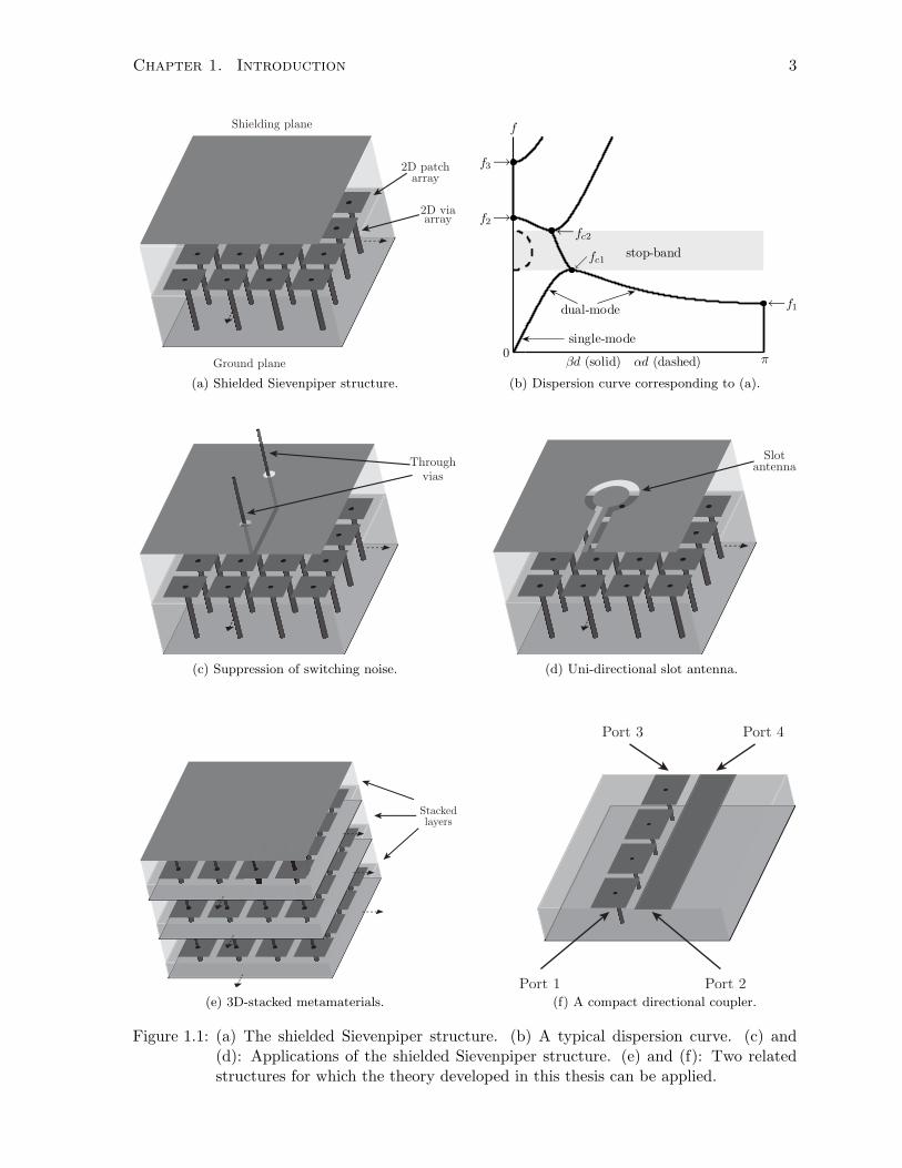
Chapter 1. Introduction 3
2D patcharray
2D viaarray
Shielding plane
Ground plane
(a) Shielded Sievenpiper structure. (b) Dispersion curve corresponding to (a).
Throughvias
(c) Suppression of switching noise.
Slotantenna
(d) Uni-directional slot antenna.
Stackedlayers
(e) 3D-stacked metamaterials.
Port 1 Port 2
Port 3 Port 4
(f) A compact directional coupler.
Figure 1.1: (a) The shielded Sievenpiper structure. (b) A typical dispersion curve. (c) and(d): Applications of the shielded Sievenpiper structure. (e) and (f): Two relatedstructures for which the theory developed in this thesis can be applied.

Chapter 1. Introduction 4
due to mode conversion. This structure is also capable of producing a slow-wave effect and thus
may be thought of as an artificial medium with enhanced effective relative permittivity [10, 11].
Closely related geometries have been shown to be useful in the creation of 3D stacked artificial
media (Figure 1.1e) which are characterized by negative effective permittivity and permeability
[12–14]. Such structures have been referred to as metamaterials. When the structure is used as
an artificial medium it is the pass-band propagation which is of primary concern. Additionally,
another topologically related geometry, a coupled-line microstrip configuration [15, 16], where
one of the lines is loaded periodically with series capacitors and shunt inductors (Figure 1.1f),
has been shown to yield a compact directional coupler. This application also relies on the
operation of the structure in the stop-band, between fc1 and fc2, however in a manner which
is different from both the antenna and switching noise applications which are described above.
The frequency regime between fc1 and fc2 defines an unusual stop-band in which a propagation-
like behaviour exists if spatially separated regions of the structure are excited in isolation. In
the case of the depicted coupler, the excitation of port 1 leads to the transmission of power to
port 2, with very little power at ports 3 and 4, for sufficiently long lines. This effect is due to
the continuous leakage of power from line 1 to line 2, and is intimately related to the unusual
nature of the complex modes.
Transmission line theory is incapable of capturing the dual-mode dispersion behaviour of
the shielded Sievenpiper structure and its derivatives, and this provides the primary motivation
for this work, which is the development of an analytical method which extends the standard
TL model by allowing for multiple modes of propagation. It will be shown that multiconductor
transmission line (MTL) theory, which is the multi-mode generalization of TL theory, is capable
of modeling the dispersion behaviour of the shielded Sievenpiper structure and its derivative
structures in a compact manner [5, 11, 17]. The shielded Sievenpiper structure will be examined
in depth and will provide a canonical example of the analytical method developed in this work.
Due to the relative simplicity of its geometry, the theory yields compact analytical formulas for
critical points on its dispersion curve, f1, f2, f3, and f4 (not shown in Figure 1.1b), along with
fc1 and fc2. The developed analytical formulation will provide one with an enhanced physical
understanding of the shielded Sievenpiper structure’s operation, and additionally allow for
intuition on the operation of the related geometries.
In the following section a review of some of the models which have been previously used to
characterize the shielded Sievenpiper structure and other related structures will be presented.

Chapter 1. Introduction 5
1.2 Background
The analytical approach which will be developed in this thesis can be best appreciated by
examining a series of structures which are related, both in terms of their geometry, and in terms
of the wave propagation effects they exhibit. Various models describing wave propagation in
these structures will be reviewed. Although each of the models will be seen to describe the
propagation phenomena within restricted regimes, they will be shown to be overly restrictive
in terms of developing an overall analytical and intuitive picture of the observed propagation
effects.
1.2.1 Sievenpiper mushroom structure
The Sievenpiper mushroom structure [18], which is depicted in Figure 1.2, is composed of a
square grid of isolated metallic (microstrip) patches which are connected to a solid ground
plane with vias. This structure has been used to reduce mutual coupling in microstrip antenna
arrays [19], perform two-dimensional beam steering [20], and to create low profile wire antennas
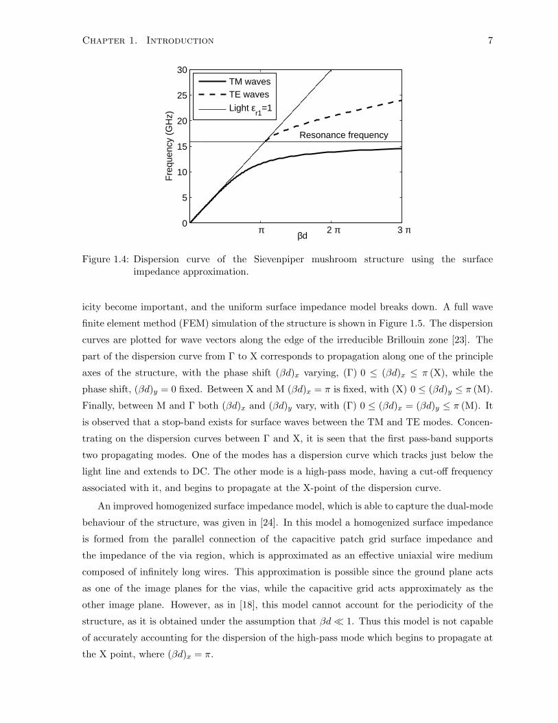
[21, 22]. It was initially modeled in [18] as a uniform surface, with the surface impedance Zsgiven by the parallel combination of an inductance, L and a capacitance, C:
Zs =jωL
1− ω2LC(1.1)
The origin of the inductance and capacitance is depicted in Figure 1.3, where it is observed that
the inductance is due to the circulation of current along a path defined by the ground plane,
the patches and the vias, and the capacitance is due to the fringing fields between the patches.
Dispersion curves, which describe the wave propagation derived from this model, are shown
in Figure 1.4, where it is observed that at low frequencies a TM (transverse magnetic) surface
wave is supported. At the resonance frequency, ω2 = 1LC , the surface impedance becomes
infinite (Zs →∞), and above it TM surface waves are cut off. However, TE (transverse electric)
surface waves are supported above the resonant frequency. As the above model assumes that the
surface impedance is uniform, the dispersion curves generated from it can only be accurate when
the electrical phase shift per-unit-cell, βd is much smaller than unity (βd 1). The condition
βd 1 corresponds to an effective wavelength which is much greater than the period, d, and in
this long wavelength limit, the effect of the periodicity may in a sense be averaged out, resulting
in the surface impedance given by (1.1). Such models are also referred to as homogenization
models, as the physical periodic (and hence non-homogenous) structure is assigned an effective
homogenous parameter (the surface impedance, Zs) to describe it.
However, when βd is of the order of magnitude of unity or greater, the effects of the period-

Chapter 1. Introduction 6
x
y
y
z
hl, ǫ2
d
d 2D patch grid
ground plane
vias
(a) Side view (b) Top view
Figure 1.2: Geometry of the Sievenpiper structure.
L
C
Figure 1.3: Origin of the the inductance, L, and capacitance, C for the surface impedancemodel.
Chapter 1. Introduction 7
0
5
10
15
20
25
30
Resonance frequency
π 2 π 3 πβd
Fre
quen
cy (
GH
z)
TM wavesTE waves
Light εr1
=1
Figure 1.4: Dispersion curve of the Sievenpiper mushroom structure using the surfaceimpedance approximation.
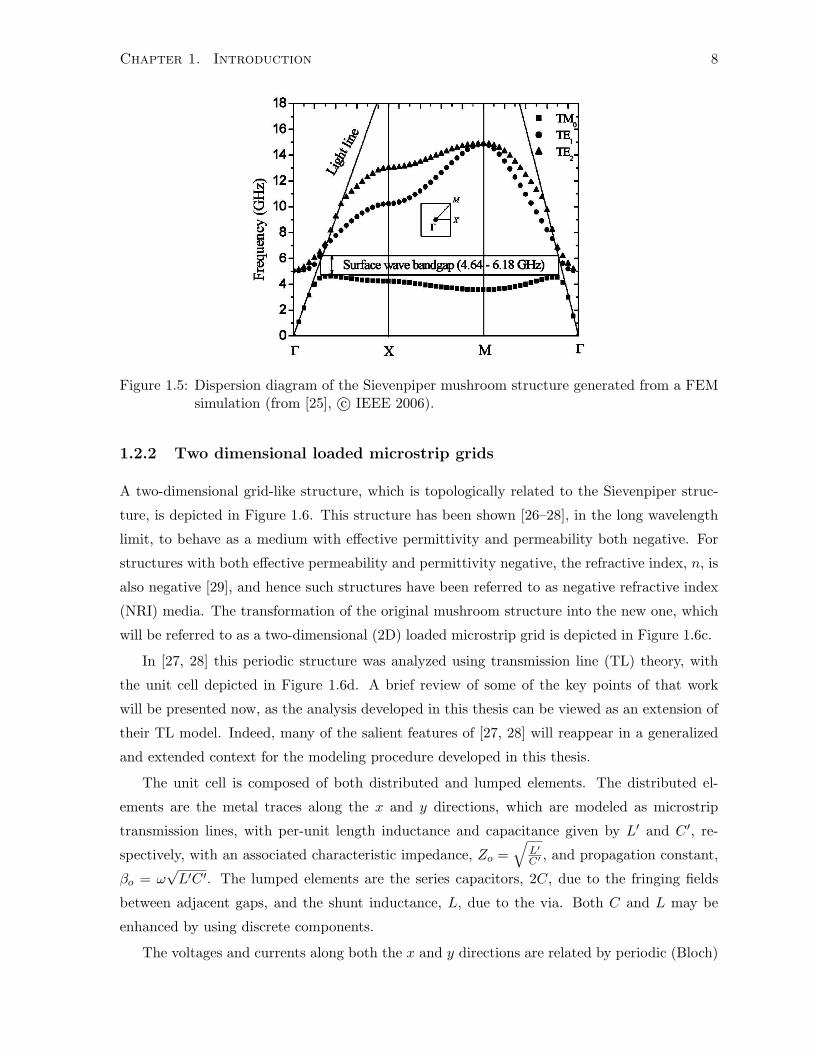
icity become important, and the uniform surface impedance model breaks down. A full wave
finite element method (FEM) simulation of the structure is shown in Figure 1.5. The dispersion
curves are plotted for wave vectors along the edge of the irreducible Brillouin zone [23]. The
part of the dispersion curve from Γ to X corresponds to propagation along one of the principle
axes of the structure, with the phase shift (βd)x varying, (Γ) 0 ≤ (βd)x ≤ π (X), while the
phase shift, (βd)y = 0 fixed. Between X and M (βd)x = π is fixed, with (X) 0 ≤ (βd)y ≤ π (M).
Finally, between M and Γ both (βd)x and (βd)y vary, with (Γ) 0 ≤ (βd)x = (βd)y ≤ π (M). It
is observed that a stop-band exists for surface waves between the TM and TE modes. Concen-
trating on the dispersion curves between Γ and X, it is seen that the first pass-band supports
two propagating modes. One of the modes has a dispersion curve which tracks just below the
light line and extends to DC. The other mode is a high-pass mode, having a cut-off frequency
associated with it, and begins to propagate at the X-point of the dispersion curve.
An improved homogenized surface impedance model, which is able to capture the dual-mode
behaviour of the structure, was given in [24]. In this model a homogenized surface impedance
is formed from the parallel connection of the capacitive patch grid surface impedance and
the impedance of the via region, which is approximated as an effective uniaxial wire medium
composed of infinitely long wires. This approximation is possible since the ground plane acts
as one of the image planes for the vias, while the capacitive grid acts approximately as the
other image plane. However, as in [18], this model cannot account for the periodicity of the
structure, as it is obtained under the assumption that βd 1. Thus this model is not capable
of accurately accounting for the dispersion of the high-pass mode which begins to propagate at
the X point, where (βd)x = π.
Chapter 1. Introduction 8
Figure 1.5: Dispersion diagram of the Sievenpiper mushroom structure generated from a FEMsimulation (from [25], c© IEEE 2006).
1.2.2 Two dimensional loaded microstrip grids
A two-dimensional grid-like structure, which is topologically related to the Sievenpiper struc-
ture, is depicted in Figure 1.6. This structure has been shown [26–28], in the long wavelength
limit, to behave as a medium with effective permittivity and permeability both negative. For
structures with both effective permeability and permittivity negative, the refractive index, n, is
also negative [29], and hence such structures have been referred to as negative refractive index
(NRI) media. The transformation of the original mushroom structure into the new one, which
will be referred to as a two-dimensional (2D) loaded microstrip grid is depicted in Figure 1.6c.
In [27, 28] this periodic structure was analyzed using transmission line (TL) theory, with
the unit cell depicted in Figure 1.6d. A brief review of some of the key points of that work
will be presented now, as the analysis developed in this thesis can be viewed as an extension of
their TL model. Indeed, many of the salient features of [27, 28] will reappear in a generalized
and extended context for the modeling procedure developed in this thesis.
The unit cell is composed of both distributed and lumped elements. The distributed el-
ements are the metal traces along the x and y directions, which are modeled as microstrip
transmission lines, with per-unit length inductance and capacitance given by L′ and C ′, re-
spectively, with an associated characteristic impedance, Zo =√
L′
C′ , and propagation constant,
βo = ω√L′C ′. The lumped elements are the series capacitors, 2C, due to the fringing fields
between adjacent gaps, and the shunt inductance, L, due to the via. Both C and L may be
enhanced by using discrete components.
The voltages and currents along both the x and y directions are related by periodic (Bloch)
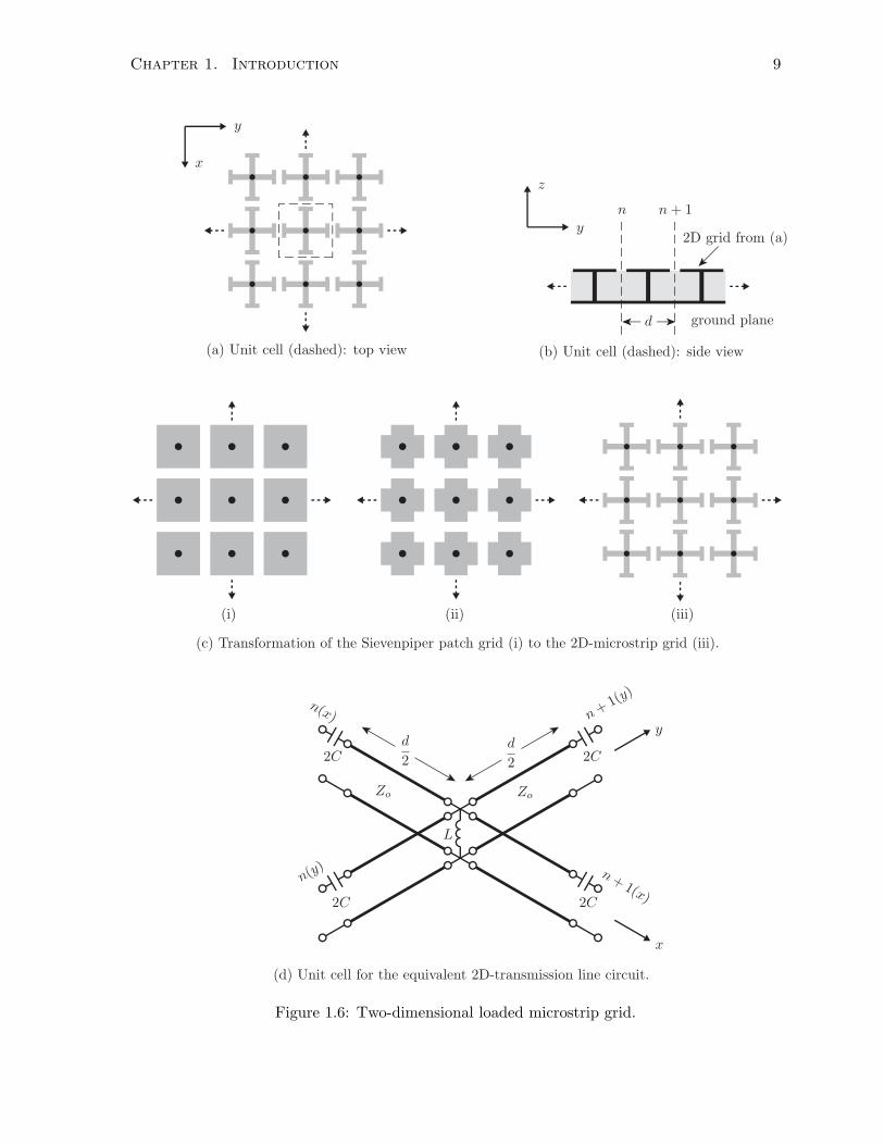
Chapter 1. Introduction 9
(i) (ii) (iii)
(c) Transformation of the Sievenpiper patch grid (i) to the 2D-microstrip grid (iii).
x
x
y
y
y
z
n n + 1
n(x)
n + 1(x)n(y)
n + 1(y)
L
2C 2C
2C 2C
Zo Zo
d
2d
2
d
2D grid from (a)
ground plane
(a) Unit cell (dashed): top view (b) Unit cell (dashed): side view
(d) Unit cell for the equivalent 2D-transmission line circuit.
Figure 1.6: Two-dimensional loaded microstrip grid.
Chapter 1. Introduction 10
boundary conditions between nodes n and n+1. Bloch’s Theorem [23] states that the field vari-
ables separated by the periodicity of the unit cell, d, are related by the Bloch propagation con-
stants, βx and βy. Along the x-direction, Vn+1(x) = Vn(x) e−jβxd and In+1(x) = In(x) e−jβxd,
with analogous relations holding along the y-direction. By transforming the voltage and cur-
rent variables at the unit cell edges, to the central connecting node, and applying Kirchhoff’s
voltage and current laws, a homogenous system of equations is obtained. Requiring that the
determinant of said system be zero, which is required for non-trivial solutions, the dispersion
equation for the structure is obtained, and given by:
cos (βxd) + cos(βyd)
= −[2 sin
(βod
2
)− 1ZoωC
cos(βod
2
)][2 sin
(βod
2
)− Zo
2ωLcos(βod
2
)]+ 2 (1.2)
A qualitative understanding of the dispersion equation may be obtained by assuming propa-
gation along the x direction, with βxd varying and βyd = 0 fixed, for which (1.2) takes the
form:
cos(βxd) = F (ω,L′, C ′, L, C) (1.3)
where F is a function of frequency (ω), the host TL parameters (L′, C ′), and the loading
elements (L and C). The periodicity of the cosine function implies that the dispersion equation
has a period 2π and thus can be restricted to the interval −π ≤ βxd ≤ π, which is referred
to as the Brillouin zone [23]. Due to the even symmetry of the cosine function, the dispersion
may be plotted in the range 0 ≤ βxd ≤ π. For lossless structures, as will be considered here,
the function F is purely real, and can have an absolute value greater than or less than 1, and
by restricting the interval to 0 ≤ βxd ≤ π, a unique solution for βxd is obtained. When |F | ≤ 1
the solution represents a purely propagating mode, and otherwise it is an evanescent mode.
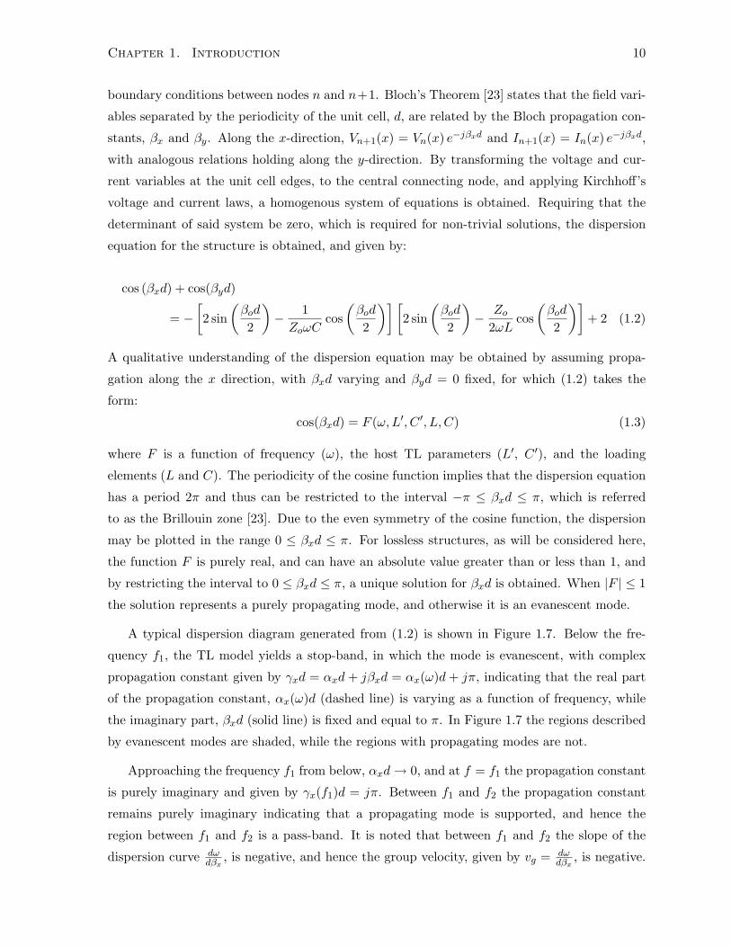
A typical dispersion diagram generated from (1.2) is shown in Figure 1.7. Below the fre-
quency f1, the TL model yields a stop-band, in which the mode is evanescent, with complex
propagation constant given by γxd = αxd+ jβxd = αx(ω)d+ jπ, indicating that the real part
of the propagation constant, αx(ω)d (dashed line) is varying as a function of frequency, while
the imaginary part, βxd (solid line) is fixed and equal to π. In Figure 1.7 the regions described
by evanescent modes are shaded, while the regions with propagating modes are not.
Approaching the frequency f1 from below, αxd→ 0, and at f = f1 the propagation constant
is purely imaginary and given by γx(f1)d = jπ. Between f1 and f2 the propagation constant
remains purely imaginary indicating that a propagating mode is supported, and hence the
region between f1 and f2 is a pass-band. It is noted that between f1 and f2 the slope of the
dispersion curve dωdβx
, is negative, and hence the group velocity, given by vg = dωdβx
, is negative.

Chapter 1. Introduction 11
Figure 1.7: Typical dispersion relation described by (1.2) for on-axis propagation with βyd = 0(fixed), and βxd varied.
0 0
1
2
3
4
5
6
7
βd
Fre
qu
en
cy (
GH
z)
π
Surface Wave
Backward Wave
FEM simulation
TL Model (BW only)
Light Line
Stopband
f3
f2
f1
Figure 1.8: Full wave FEM simulation of an NRI grid for on-axis propagation with βyd = 0(fixed), and βxd varied.

Chapter 1. Introduction 12
However, the phase velocity vφ = ωβx
, is positive, indicating that the band between between f1
and f2 supports a backward wave (BW) mode [30].
Between f2 and f3, the second stop-band is encountered, with an evanescent mode sup-
ported, while the second pass-band resides between f3 and f4. In the region between f3 and f4
the group and phase velocities are both positive, indicating that a forward wave (FW) mode is
supported. This alternating sequence of stop-bands and pass-bands subsequently repeats itself.
A FEM simulation for such a structure is shown in Figure 1.8. The BW mode predicted
by the TL model is captured by the FEM simulation, but in addition, a FW surface wave
mode, whose dispersion is just below the light line, is also supported, which the TL model does
not account for. Contra-directional coupling between the FW and BW modes yields a stop-
band, which was also observed for the original Sievenpiper structure, as shown in Figure 1.5.
Qualitatively the dispersion curves for the 2D-grid and the Sievenpiper structure are identical;
however due to the use of discrete components to enhance C and L, the 2D-grid typically
has a larger BW bandwidth. From the FEM simulations the field structure of each mode is
obtained. For the BW mode, the fields are largely concentrated in the substrate (between the
traces and the ground). For the FW mode, the fields are largely concentrated in the air above
the substrate. Additionally, the FEM simulations reveal that the TL model is accurate at the
Bragg resonance (f1 at βxd = π), which is out of the range of applicability of the previously
discussed homogenization models [18, 24].
A simplified understanding of the dispersion for this structure may be obtained by assuming
that the Bloch phase shifts across a unit cell are small, βxd 1 and βyd 1, and these ap-
proximations, with the additional assumption that the interconnecting microstrip TL segments
are also electrically short, βod 1, result in the exact TL dispersion, (1.2) reducing to:
β2x + β2
y = ω2
(L′ − 1
ω2Cd
)(2C ′ − 1
ω2Ld
)(1.4)
In [28] it was shown that (1.4) may be written as:
β2 = ω2µeff εeff (1.5)
with
µeff =(L′ − 1
ω2Cd
)(1.6)
εeff =(
2C ′ − 1ω2Ld
)(1.7)
where µeff and εeff are the effective permeability and permittivity of the structure. The
Chapter 1. Introduction 13
dispersion equation (1.5) shows that under the conditions βxd 1, βyd 1, and βod 1,
the structures appears homogenous and isotropic. At low enough frequencies it is clear that
both µeff and εeff are less than zero, indicating that the effective medium parameters are
negative. As ω → 0, both parameters approach −∞ and the approximate dispersion equation
(1.4) predicts that the structure supports a propagating mode. This is inconsistent with the
results of the exact dispersion equation (1.2), which predicts that the BW mode is cut-off below
f1. This inconsistency arises because the approximations which lead to (1.4), βxd 1, βyd 1,
are not satisfied at very low frequencies. However as frequency increases and approaches f2,
both µeff and εeff remain negative and the conditions βxd 1, βyd 1 are satisfied. Thus,
in the region just below f2, the structure behaves in a homogenous and isotropic manner, with
negative material parameters. Within this region the structure supports a BW mode, and hence
the effective negative material parameters are associated with a BW band. It is observed from
(1.6) and (1.7) that the existence of the BW band is reliant upon the presence of both L and
C, and if either of these loading elements were removed from the structure the BW band would
be eliminated as well.
The frequency f2 is obtained by setting one of µeff or εeff equal to zero, with f3 determined
by setting the excluded case equal to zero. These frequencies depend on the loading elements,
L and C, and the distributed parameters, L′ and C ′, and are given by:
ω22 = min
1
C(L′d),
1L(2C ′d)
(1.8)
ω23 = max
1
C(L′d),
1L(2C ′d)
(1.9)
Both f2 and f3 describe resonances occurring between one of the loading elements, L, C,
and one of the distributed TL parameters (multiplied by the periodicity, d), L′d, 2C ′d. At
this point it is possible to justify the conditions under which the short TL approximation,
βod 1, could be made in obtaining (1.4). Each of f2 and f3 contain one of the loading
elements, L and C individually. By making L and C large enough it is possible to reduce
f2 and f3 to arbitrarily low values, ensuring that βod 1 is satisfied. In [31], it was noted
that homogenization models of the mushroom structure are only accurate when the gap spacing
between patches, g is sufficiently small, and the substrate height, hl is sufficiently large. In terms
of the present analysis such conditions correspond to a large series capacitance, C, and a large
shunt inductance, L, and thus the TL model described here provides an elegant explanation
of conditions under which homogenization is accurate. However, in the case that L and C are
not large, so that the short TL approximation (βod 1) can’t be made for the interconnecting
microstrip lines, the full dispersion equation (1.2), remains accurate and should be used rather
than the approximate one, (1.4).
Chapter 1. Introduction 14
The operation of such a structure as a NRI medium relies on the utilization of the BW
mode band, as was explained earlier. However the FEM simulation (Figure 1.8) revealed that
the BW mode bandwidth was reduced due to the stop-band formed by the contra-directional
coupling of the FW and BW modes. Additionally, in regions where the BW is propagating, a
FW mode is also supported, so that the structure is fundamentally a dual-mode structure. In
[26] it was demonstrated that as long as the operating frequency is away from the stop-band,
the FW mode has a negligible impact on the analysis, as long as the excitation mechanism
of the structure is such that the source is situated between the microstrip grid layer and the
ground plane. This is consistent with the fact that the field structure of the BW mode is largely
confined to the substrate, while the field structure of the FW mode is largely confined to the
air region above the substrate. However, as the BW and the FW modes coalesce and form a
stop-band, the TL model breaks down, and excitations with frequencies close to, or within this
stop-band, cannot be modeled with a simple TL analysis.
Finally it is noted that a similar TL analysis can be applied to the original mushroom
structure, with a fundamental BW mode predicted. However, the fact that the FW mode is
not accounted for would again be an obvious major deficiency in the completeness of such a
model.
1.2.3 Shielded Sievenpiper structure
In the previous two subsections the Sievenpiper structure, and the topologically related 2D
microstrip grid were examined. Another structure, which is related to these two structures
is the shielded Sievenpiper structure, which is simply the original Sievenpiper structure from
Figure 1.2, with an additional conducting shielding plane above the mushroom layer. A unit
cell of the shielded structure is depicted in Figure 1.9. The structure consists of a lower region
of height hl and permittivity ε2 and an upper region of height hu and permittivity ε1. The
shielded structure has been shown to be useful in the suppression of switching noise in digital
circuits [6–8], and in the creation of unidirectional slot antennas [9].
Several analytical models for this structure have been proposed, but before describing them
it will be interesting and useful to compare full wave FEM simulations of the shielded structure
with the TL analysis of Section 1.2.2, which predicted an initial high pass BW band. In
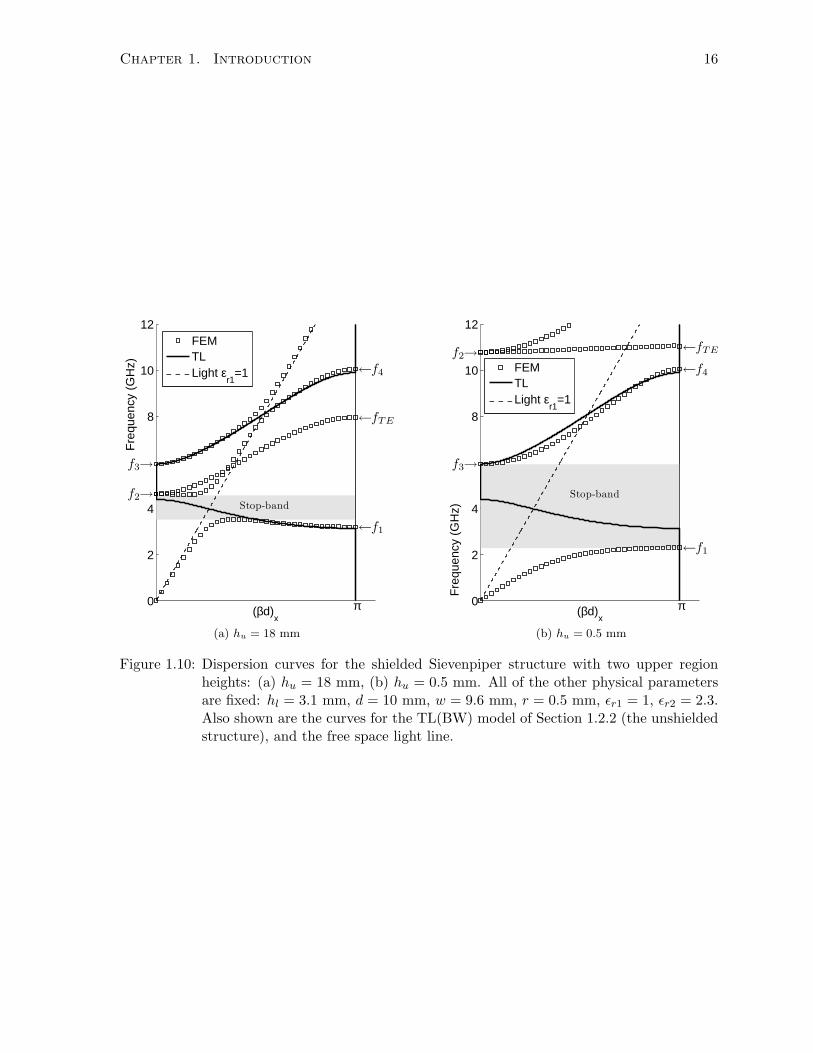
Figure 1.10 dispersion curves corresponding to two sets of simulations with varying upper
region height, (a) hu = 18 mm, and (b) hu = 0.5 mm are shown. All of the other physical
parameters are fixed: hl = 3.1 mm, d = 10 mm, w = 9.6 mm, r = 0.5 mm, εr1 = 1, εr2 = 2.3.
For the larger value of hu = 18 mm, the FEM generated dispersion curve shown in Fig-
ure 1.10a bears a strong resemblance to that of both the unshielded structure (Figure 1.5) and
the 2D microstrip grid (Figure 1.8). The first band is dual mode, with a FW and a BW mode.

Chapter 1. Introduction 15
hu
hl
ǫ1
ǫ2
Patch conductor; w
Shielding conductor; d
Ground conductor
via; r
Figure 1.9: Unit cell of the shielded Sievenpiper structure.
The fields of the FW mode are largely concentrated in the upper region, while the fields of the
BW mode are largely concentrated in the lower region. The TL model dispersion is accurate
away from the light line, with the resonances, f1, f2, f3 and f4 captured by the FEM simu-
lations. However the TL model does not capture the low frequency FW mode and hence is
incapable of accounting for the stop-band, which is due to contra-directional coupling of the
FW and the BW modes.
For the smaller value of hu = 0.5 mm, shown in Figure 1.10b the dispersion is qualitatively
altered. The lowest pass-band becomes single mode, with the BW mode eliminated. The FW
mode has a significantly smaller slope than for the larger (hu = 18 mm) value, indicating that
a strong slow wave effect is achieved. Additionally, the stop-band bandwidth is substantially
increased. The resonant frequency f1 is shifted down, while f2 is shifted up, and neither
corresponds to those of the TL model. However, the frequencies f3 and f4 predicted by the TL
model are captured by the FEM simulation. The fact that the f3 and f4 seem to be invariant
as the upper region height, hu, is altered, is an interesting phenomenon which will be explained
by the theory developed in this thesis.
Several analytical models for the dispersion analysis of the shielded structure have been de-
veloped. In [6] the surface impedance model of [18] was used in conjunction with the transverse
resonance technique to determine the lowest modes of the structure. This technique predicts a
low frequency band with a single FW TM mode, followed by a stop-band, and then an upper
TE mode. The use of the surface impedance model precludes the possibility of accurately pre-
dicting the dispersion near the Brillouin zone boundary (βd = π). However, it was found that
as long as the upper region height, hu is relatively small, such a model provides a reasonable
estimate for the edges of the pass-band.
In [7, 8] the structure was modeled as a loaded transmission line (TL). These TL models are
different than the one described in Section 1.2.2, as they attempt to incorporate the effect of the
upper shielding conductor. The model introduced in [8] will be examined below, and from here
Chapter 1. Introduction 16
0
2
4
8
10
12
←f1
f2→
f3→
←fTE
←f4
Stop-band
π(βd)x
Fre
quen
cy (
GH
z)
FEMTLLight ε
r1=1
(a) hu = 18 mm
0
2
4
8
10
12
←f1
f2→
f3→
←fTE
←f4
Stop-band
π(βd)x
Fre
quen
cy (
GH
z)
FEMTLLight ε
r1=1
(b) hu = 0.5 mm
Figure 1.10: Dispersion curves for the shielded Sievenpiper structure with two upper regionheights: (a) hu = 18 mm, (b) hu = 0.5 mm. All of the other physical parametersare fixed: hl = 3.1 mm, d = 10 mm, w = 9.6 mm, r = 0.5 mm, εr1 = 1, εr2 = 2.3.Also shown are the curves for the TL(BW) model of Section 1.2.2 (the unshieldedstructure), and the free space light line.
Chapter 1. Introduction 17
n
n
n + 1
n + 1
Y YL (via)
C =ǫ1w
hud
hu, ǫ1
hl, ǫ2
Zo =
√L′
C ′
Zo Zo
w
d
2d
2
d
Shielding plane
ground plane
(a) Unloaded 2 conductor TL (b) Transformation into a loaded TL
(c) Equivalent TL circuit (d) Composition of Y
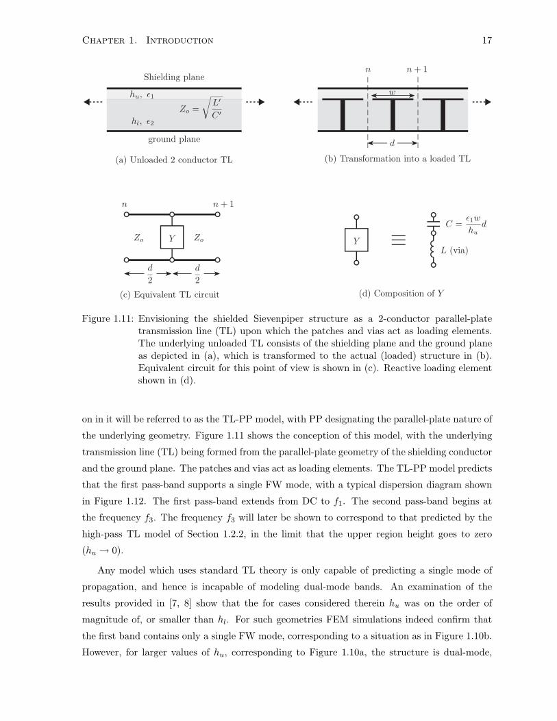
Figure 1.11: Envisioning the shielded Sievenpiper structure as a 2-conductor parallel-platetransmission line (TL) upon which the patches and vias act as loading elements.The underlying unloaded TL consists of the shielding plane and the ground planeas depicted in (a), which is transformed to the actual (loaded) structure in (b).Equivalent circuit for this point of view is shown in (c). Reactive loading elementshown in (d).
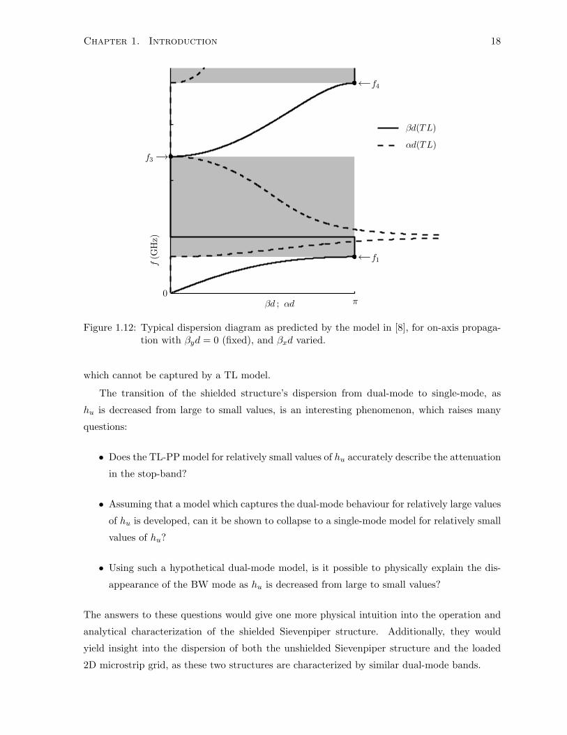
on in it will be referred to as the TL-PP model, with PP designating the parallel-plate nature of
the underlying geometry. Figure 1.11 shows the conception of this model, with the underlying
transmission line (TL) being formed from the parallel-plate geometry of the shielding conductor
and the ground plane. The patches and vias act as loading elements. The TL-PP model predicts
that the first pass-band supports a single FW mode, with a typical dispersion diagram shown
in Figure 1.12. The first pass-band extends from DC to f1. The second pass-band begins at
the frequency f3. The frequency f3 will later be shown to correspond to that predicted by the
high-pass TL model of Section 1.2.2, in the limit that the upper region height goes to zero
(hu → 0).
Any model which uses standard TL theory is only capable of predicting a single mode of
propagation, and hence is incapable of modeling dual-mode bands. An examination of the
results provided in [7, 8] show that the for cases considered therein hu was on the order of
magnitude of, or smaller than hl. For such geometries FEM simulations indeed confirm that
the first band contains only a single FW mode, corresponding to a situation as in Figure 1.10b.
However, for larger values of hu, corresponding to Figure 1.10a, the structure is dual-mode,
Chapter 1. Introduction 18
Figure 1.12: Typical dispersion diagram as predicted by the model in [8], for on-axis propaga-tion with βyd = 0 (fixed), and βxd varied.
which cannot be captured by a TL model.
The transition of the shielded structure’s dispersion from dual-mode to single-mode, as
hu is decreased from large to small values, is an interesting phenomenon, which raises many
questions:
• Does the TL-PP model for relatively small values of hu accurately describe the attenuation
in the stop-band?
• Assuming that a model which captures the dual-mode behaviour for relatively large values
of hu is developed, can it be shown to collapse to a single-mode model for relatively small
values of hu?
• Using such a hypothetical dual-mode model, is it possible to physically explain the dis-
appearance of the BW mode as hu is decreased from large to small values?
The answers to these questions would give one more physical intuition into the operation and
analytical characterization of the shielded Sievenpiper structure. Additionally, they would
yield insight into the dispersion of both the unshielded Sievenpiper structure and the loaded
2D microstrip grid, as these two structures are characterized by similar dual-mode bands.

Chapter 1. Introduction 19
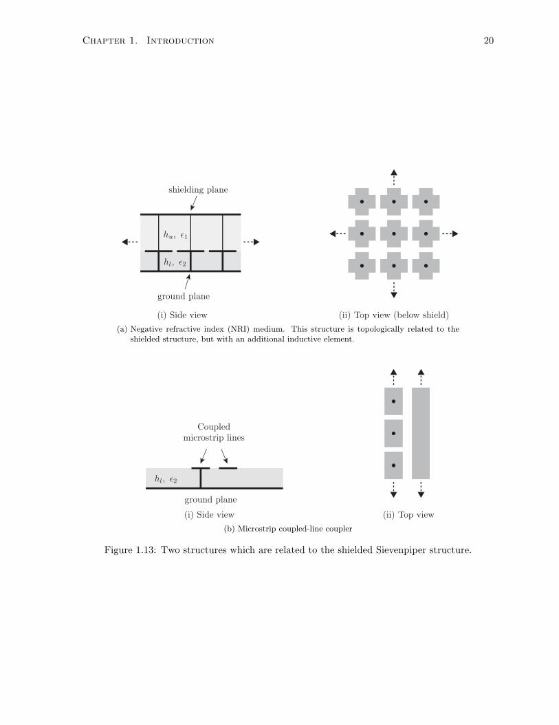
1.2.4 Some other related geometries
Examples of other related geometries for which the theory developed in this thesis has been
applied to are shown in Figure 1.13. The first of these structures has the topology of the
shielded structure, but with the addition of an extra inductive element connecting the patch
plane to the upper shielding plane. By adding this inductive element it is possible to eliminate
the FW mode of the shielded structure, while simultaneously increasing the BW bandwidth.
Hence this geometry has been shown to be useful in the design of large bandwidth NRI media
as shown in [12, 13], with a related geometry given in [14]. The theory developed in this thesis
can be used to model the dispersion of these modified shielded structures, and also in physically
explaining the conception of such geometries.
The second structure is a microstrip coupled-line geometry, where one of the lines has been
loaded with series capacitors and shunt inductors. The dispersion of this structure is also dual-
mode in the lowest band. Interestingly, the operation of such a coupler is intimately related to
the nature of the modes which exist in the first stop-band [15, 16], as will be described later in
this thesis.
1.2.5 Commentary
The unshielded Sievenpiper structure, the 2D-loaded microstrip grid, and the shielded Sieveniper
structure all exhibit dual-mode dispersion curves in their lowest bands. Dispersion curves gen-
erated by the previously described approximate models are shown in Figure 1.14, along with a
typical dual-mode dispersion curve which all three geometries exhibit.
Although the dual-mode behaviour may be accounted for by homogenization models, such
models are not accurate near the Bragg resonance at βd = π. Additionally, as was demonstrated
in [31], the condition βd 1 is not sufficient for such models to be accurate, and in general
they are restricted to low frequencies, where both the guided and free space wavelengths are
much larger than the periodicity.
The transmission line (TL) models, on the other hand, are capable of accounting for the
periodicity of the structure, and hence are accurate at the Bragg resonance condition, βd =
π. Additionally, TL models provide for a simple and intuitive understanding of the wave
propagation, and yield compact formulas for band-edges. However TL models are deficient
in that they inherently only account for a single mode, and hence are incapable of capturing
dual-mode behaviour. However the physical intuition obtained from TL models makes them
highly appealing, and this aspect would be desirable in any enhanced analysis which takes into
account dual-mode, or in general multi-mode propagation bands.
Chapter 1. Introduction 20
hu, ǫ1
hl, ǫ2
shielding plane
ground plane
(i) Side view (ii) Top view (below shield)(a) Negative refractive index (NRI) medium. This structure is topologically related to the
shielded structure, but with an additional inductive element.
hl, ǫ2
ground plane
Coupledmicrostrip lines
(i) Side view (ii) Top view(b) Microstrip coupled-line coupler
Figure 1.13: Two structures which are related to the shielded Sievenpiper structure.

Chapter 1. Introduction 21
Res. freq.
π 2 π 3 πβd
freq
uenc
yTMTELight
(i) Surface imp. (Zs) model
(ii) Top view
hl, ǫ2
air
(iii) Side view(a)
(i) TL (BW) model
(ii) Top view
hl, ǫ2
air
(iii) Side view(b)
(i) TL-PP model
(ii) Top view (below shield)
hu, ǫ1
hl, ǫ2
shielding plane
(iii) Side view(c)
(d)
Figure 1.14: Three related structures with dispersion curves obtained from approximatesingle-mode models: (a) the unshielded Sievenpiper structure (effective surfaceimpedance model), (b) the 2-D microstrip gird (TL-BW model), and (c) theshielded Sievenpiper structure (TL-PP model). In general all three structuresexhibit dual-mode behaviour as shown in (d).

Chapter 1. Introduction 22
1.3 Thesis Contributions and Outline
This thesis attempts to bridge the gap between the simplicity of TL models, and the accuracy
and generality achievable by full wave numerical techniques. It will be shown that multicon-
ductor transmission line (MTL) theory can be used to model both multi-mode behaviour and
periodicity, in a coherent, compact manner.
Multiconductor transmission line theory [32] is the generalization of TL theory to the case
where the number of parallel conductors is greater than two. For such geometries the per-unit
length inductance and capacitance, L′ and C ′, are transformed into n by n matrices, L′ and C′,
characterizing the coupling of the n+1 conductors, the case n = 1 being described by standard
TL theory. MTL theory characterizes the quasi-TEM modes in a system of n + 1 conductors,
showing that such geometries support n such modes. In the quasi-static limit the matrices L′
and C′ are functions of the geometry and the permeability and permittivity of the surrounding
medium alone. The theory has also been applied to situations where these matrices have more
complicated (frequency dependent) terms, modeling structures which exhibit dispersive effects,
due to the continuous reactive loading of the lines [33–35]. Such treatments are related to
MTL-homogenization approximations, as will be shown in this work.
A literature search revealed that the consideration of MTL geometries in which the loading
is modeled in a discrete manner (as in the case of the TL models described previously) has not
been extensively examined. In [36] a system in which n uniform uncoupled transmission lines
are periodically reactively loaded in a discrete manner was examined. It was shown that such
a configuration yields a total of n modes, some of which are propagating and some of which
are evanescent; i.e. of the exact type predicted by standard TL theory. The theory developed
in this work characterizes the more realistic case in which the n + 1 lines are coupled. This
feature will in turn be shown to have a critical effect on the nature of the derivable propagation
constants, with a new class of modes, which are separated from standard propagating and
evanescent modes, becoming possible.
The MTL model will be developed explicitly and in considerable detail for the shielded
Sievenpiper structure [5, 11, 17]. This is an attractive structure to study for several reasons.
As mentioned previously this geometry has been shown to be useful in the suppression of
switching noise in digital circuits [6–8] and in the creation of unidirectional slot antennas [9].
The structure is also capable of producing a strong slow-wave effect due to an enhanced effective
relative permittivity [10, 11]. Other closely related shielded geometries have been shown to be
relevant in the characterization of 3D stacked NRI metamaterials [12–14]. Another topologically
related coupled-line microstrip geometry [15, 16], has been shown to yield a compact directional
coupler. From an analytical perspective, the geometry of the shielded structure lends itself to
Chapter 1. Introduction 23
the matrices L′ and C′ taking on extremely simple forms, their components related to simple
parallel-plate type geometries. The fact that L′ and C′ can be described by simple closed form
expressions for a realistic geometric configuration will aid greatly in the interpretation of the
analytical results.
The remainder of the thesis is organized as follows. In Chapter 2 finite element method
(FEM) simulations of the shielded Sievenpiper structure will be presented. Both dispersion
curves and modal field profiles will be shown, and by examining these, several insights into the
structure of the sought after multi-mode model will be obtained.
Chapter 3 builds on the insights obtained in the previous chapter and will be focused on
developing fundamental building blocks which will subsequently be used to model the shielded
structure. These building blocks are comprised of both distributed elements, the matrices L′
and C′ which describe propagation along uniform multiconductor transmission lines, and the
reactive loading elements L and C, which describe the discontinuities due to the vias and gaps
between the patches.
In Chapter 4 a periodic multiconductor transmission line unit cell of the shielded structure
is presented and a corresponding dispersion equation will be derived from it. A comprehensive
account of the salient features described by the dispersion equation will be given. In particular,
the MTL model is readily able to handle the dual-mode behaviour of the structure. The nature
of the modes in the stop-band will be determined, where it will be shown that the first stop-band
is characterized by unusual modes: complex modes [37, 38], which are generated in pairs defined
by complex-conjugate propagation constants, γ1,2 = α(ω) ± jβ(ω). Both α(ω) and β(ω) are
functions of frequency, and critically, such modes are shown to arise even though the structure is
modeled as lossless. The MTL model will also be able to provide an explanation for the changing
character of the dispersion as hu is decreased. In particular, as was noted previously, for small
values of hu, the first pass-band is single mode, with the BW band completely eliminated. Using
the developed theory, analytical formulas for several critical points on the dispersion curves will
be derived, with these formulas revealing the mechanism behind this qualitative change in
behaviour (dual to single-mode). The MTL model will be compared with FEM simulations,
with excellent correspondence demonstrated.
In Chapter 5 the low frequency response of the shielded structure will be obtained. By
examining both the dispersion and the modal eigenvector in the low frequency limit an elegant
physical explanation of the resulting slow wave effect will be given.
In Chapter 6 excitations of a finite cascade of unit cells of the shielded structure will be
examined, with generalized scattering parameters derived. The dispersion analysis of Chapter 4
corresponds to the Bloch modes of an (infinite) periodic structure. In a finite structure a super-
position of Bloch modes will be excited and by examining the scattering parameters along with

Chapter 1. Introduction 24
the related modal excitation strengths additional insights into the operation of the structure
will be obtained. Excellent agreement between the MTL model and FEM simulations will be
shown in pass-bands and both complex mode and evanescent mode bands, thus confirming the
existence of complex modes in the structure.
In Chapter 7 a physical application which utilizes the stop-band property of the shielded
structure will be shown. A uni-directional slot antenna, which resonates within the stop-band
of the shielded structure, will be constructed and tested, demonstrating the usefulness of the
structure in suppressing the undesirable back radiation inherent in slot radiators.
In Chapter 8 a summary of the thesis contributions is presented and publications associated
with this work are listed.

Chapter 2
Analytical Motivation: Finite
Element Method Simulations
2.1 Introduction
In the preceding chapter several examples of structures with dual-mode dispersion curves were
presented. Two were open structures, the unshielded Sievenpiper structure, and the loaded NRI
2-D transmission line grid, while one was a closed structure, the shielded Sievenpiper structure.
Although the dual-mode behaviour could be explained using homogenization approximations,
these models could not account for the periodicity of the structure. Transmission line models
suffered from the opposite defect; they could account for the periodicity, but not for the dual-
mode behaviour.
In this chapter we will investigate more closely the full electromagnetic dispersion behaviour
of the shielded Sievenpiper structure using finite element method (FEM) simulations. The main
purpose of the simulations will be to provide motivation for the analytical model which will
be developed in the following chapters. FEM generated dispersion curves will be shown for a
range of values of the geometric parameters of the shielded structure. In order to develop an
intuitive understanding of the structure, a sequence of dispersion curves with varying upper
region height, hu will be presented. Previously it was seen that for relatively large hu, the
structure exhibited lowest band dual-mode behaviour, while for small enough hu the structure
had a single-mode lowest pass-band. Along with the FEM generated dispersion curves, two
additional sets of curves will be shown. These will be the TL-theory curves for the unshielded
Sievenpiper structure, which exhibit a high-pass BW pass-band, and the light line for free space
(as εr = 1 for the upper region of the simulated structure).
However, the dispersion curves alone do not in themselves provide adequate insight into
the development of the sought after dual-mode model. To this end, field profiles for modes
25
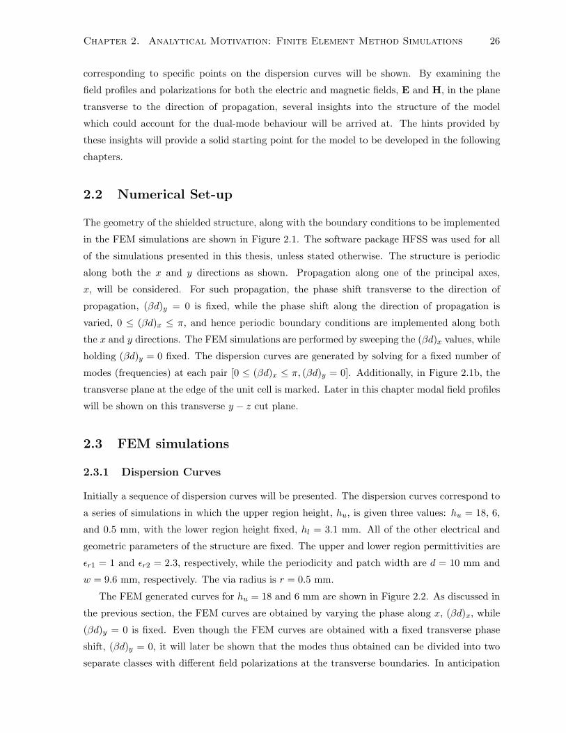
Chapter 2. Analytical Motivation: Finite Element Method Simulations 26
corresponding to specific points on the dispersion curves will be shown. By examining the
field profiles and polarizations for both the electric and magnetic fields, E and H, in the plane
transverse to the direction of propagation, several insights into the structure of the model
which could account for the dual-mode behaviour will be arrived at. The hints provided by
these insights will provide a solid starting point for the model to be developed in the following
chapters.
2.2 Numerical Set-up
The geometry of the shielded structure, along with the boundary conditions to be implemented
in the FEM simulations are shown in Figure 2.1. The software package HFSS was used for all
of the simulations presented in this thesis, unless stated otherwise. The structure is periodic
along both the x and y directions as shown. Propagation along one of the principal axes,
x, will be considered. For such propagation, the phase shift transverse to the direction of
propagation, (βd)y = 0 is fixed, while the phase shift along the direction of propagation is
varied, 0 ≤ (βd)x ≤ π, and hence periodic boundary conditions are implemented along both
the x and y directions. The FEM simulations are performed by sweeping the (βd)x values, while
holding (βd)y = 0 fixed. The dispersion curves are generated by solving for a fixed number of
modes (frequencies) at each pair [0 ≤ (βd)x ≤ π, (βd)y = 0]. Additionally, in Figure 2.1b, the
transverse plane at the edge of the unit cell is marked. Later in this chapter modal field profiles
will be shown on this transverse y − z cut plane.
2.3 FEM simulations
2.3.1 Dispersion Curves
Initially a sequence of dispersion curves will be presented. The dispersion curves correspond to
a series of simulations in which the upper region height, hu, is given three values: hu = 18, 6,
and 0.5 mm, with the lower region height fixed, hl = 3.1 mm. All of the other electrical and
geometric parameters of the structure are fixed. The upper and lower region permittivities are
εr1 = 1 and εr2 = 2.3, respectively, while the periodicity and patch width are d = 10 mm and
w = 9.6 mm, respectively. The via radius is r = 0.5 mm.
The FEM generated curves for hu = 18 and 6 mm are shown in Figure 2.2. As discussed in
the previous section, the FEM curves are obtained by varying the phase along x, (βd)x, while
(βd)y = 0 is fixed. Even though the FEM curves are obtained with a fixed transverse phase
shift, (βd)y = 0, it will later be shown that the modes thus obtained can be divided into two
separate classes with different field polarizations at the transverse boundaries. In anticipation
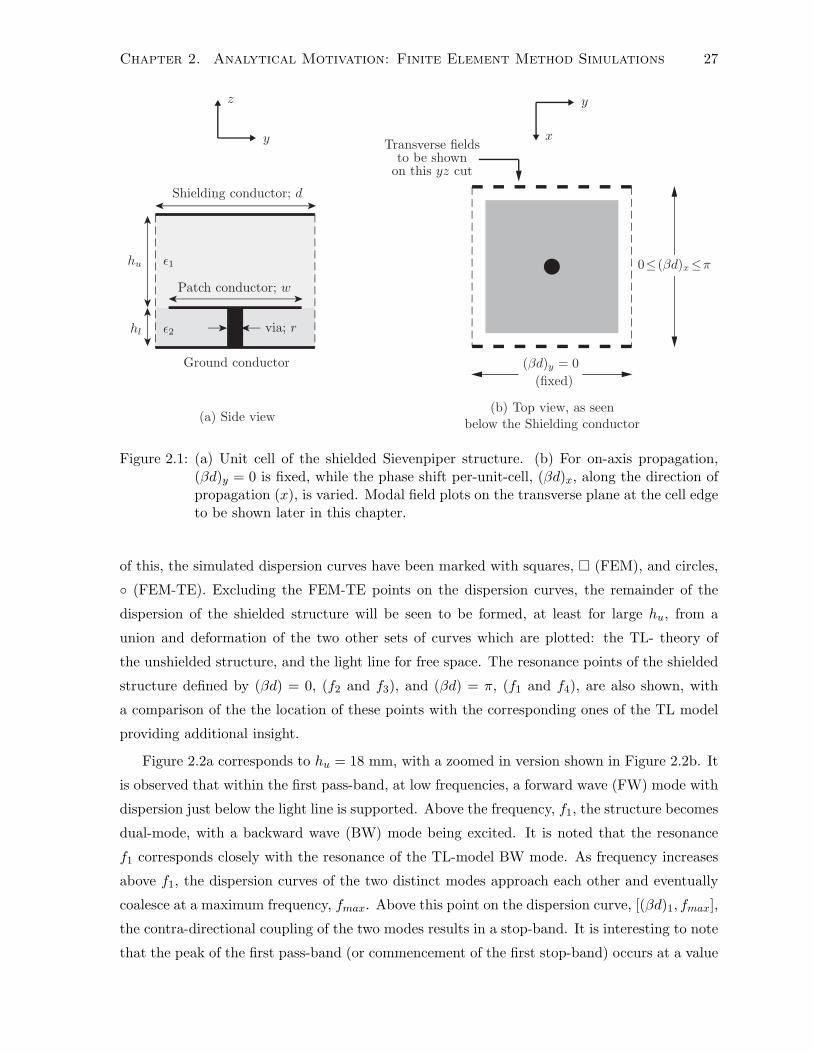
Chapter 2. Analytical Motivation: Finite Element Method Simulations 27
0≤(βd)x≤π
(βd)y = 0(fixed)
x
y
y
z
hu
hl
ǫ1
ǫ2
Patch conductor; w
Shielding conductor; d
Transverse fieldsto be shown
on this yz cut
Ground conductor
via; r
(a) Side view(b) Top view, as seen
below the Shielding conductor
Figure 2.1: (a) Unit cell of the shielded Sievenpiper structure. (b) For on-axis propagation,(βd)y = 0 is fixed, while the phase shift per-unit-cell, (βd)x, along the direction ofpropagation (x), is varied. Modal field plots on the transverse plane at the cell edgeto be shown later in this chapter.
of this, the simulated dispersion curves have been marked with squares, (FEM), and circles,
(FEM-TE). Excluding the FEM-TE points on the dispersion curves, the remainder of the
dispersion of the shielded structure will be seen to be formed, at least for large hu, from a
union and deformation of the two other sets of curves which are plotted: the TL- theory of
the unshielded structure, and the light line for free space. The resonance points of the shielded
structure defined by (βd) = 0, (f2 and f3), and (βd) = π, (f1 and f4), are also shown, with
a comparison of the the location of these points with the corresponding ones of the TL model
providing additional insight.
Figure 2.2a corresponds to hu = 18 mm, with a zoomed in version shown in Figure 2.2b. It
is observed that within the first pass-band, at low frequencies, a forward wave (FW) mode with
dispersion just below the light line is supported. Above the frequency, f1, the structure becomes
dual-mode, with a backward wave (BW) mode being excited. It is noted that the resonance
f1 corresponds closely with the resonance of the TL-model BW mode. As frequency increases
above f1, the dispersion curves of the two distinct modes approach each other and eventually
coalesce at a maximum frequency, fmax. Above this point on the dispersion curve, [(βd)1, fmax],
the contra-directional coupling of the two modes results in a stop-band. It is interesting to note
that the peak of the first pass-band (or commencement of the first stop-band) occurs at a value

Chapter 2. Analytical Motivation: Finite Element Method Simulations 28
0
2
4
8
10
12
←f1
f2→
f3→
←fTE
←f4
Stop-band
π(βd)x
Fre
quen
cy (
GH
z)
FEMFEM (TE)TLLight ε
r1=1
(a) hu = 18 mm
1
2
3
4
5
←f1
f2→
f3→
↑[(βd)1 , fmax
]
↑[(βd)2 , fmin
] Stop-band
π(βd)x
FEMFEM (TE)TLLight ε
r1=1
(b) hu = 18 mm; zoom in of (a)
0
2
4
8
10
12
←f1
f2−→f3→
←fTE
←f4
Stop-band
π(βd)x
Fre
quen
cy (
GH
z)
FEMFEM (TE)TLLight ε
r1=1
(c) hu = 6 mm
1
2
3
4
5
FW 1
BW 1
BW 2
TE
FW 2
←f1
f2→f3→
↑[(βd)1 , fmax
]
↑[(βd)2 , fmin
]Stop-band
π(βd)x
FEMFEM (TE)TLLight ε
r1=1
(d) hu = 6 mm; zoom in of (c)
Figure 2.2: Dispersion curves for the shielded structure with varying upper region height: (a),(b) hu = 18 mm; (c), (d) hu = 6 mm. All of the other physical parameters arefixed: hl = 3.1 mm, d = 10 mm, w = 9.6 mm, r = 0.5 mm, εr1 = 1, εr2 = 2.3. Alsoshown are the curves for the TL(BW) model of the unshielded structure, and thefree space light line. Field plots corresponding to the points labeled in (d) will beshown later in this chapter.

Chapter 2. Analytical Motivation: Finite Element Method Simulations 29
0
2
4
8
10
12
FW 1
FW 2←f1
f2→
f3→
←fTE
←f4
Stop-band
π(βd)x
Fre
quen
cy (
GH
z)
FEMFEM (TE)TLLight ε
r1=1
Figure 2.3: Dispersion curves for the shielded structure with with hu = 0.5 mm. The otherphysical parameters are: hl = 3.1 mm, d = 10 mm, w = 9.6 mm, r = 0.5 mm,εr1 = 1, εr2 = 2.3. Also shown are the curves for the TL(BW) model of theunshielded structure, and the free space light line. Field plots corresponding to thelabeled points will be shown later in this chapter.
of (βd) 6= 0 or π, which is an indication that the stop-band is not of the type more typically
encountered for periodic structures. The dispersion in this first band is seen to be roughly a
combination of the FW light line and the BW of the TL model, except in the region where
these two curves coalesce, above which a stop-band is formed.
In the second pass-band, it is observed that f2 is a point of modal degeneracy, with both
a FW (TE) and a BW mode emerging from f2. Disregarding the FW (TE) mode, it is again
observed that the dispersion curve is formed from a combination of the BW emerging from
f2 and the light line, with the peak of the stop-band at [(βd)2, fmin] formed due to contra-
directional coupling of the BW and the FW modes. It is noted that the BW mode emerging
from f2 is close to, but shifted up slightly, relative to that of the TL theory curve. The phase
shifts at the commencement and conclusion of the stop band, (βd)1 and (βd)2, are not 0 or π,
but 0 ≤ (βd)2 < (βd)1 < π, which again is an indication that the stop-band is not of the type
more typically encountered for periodic structures.
Continuing with Figure 2.2a, at f3, which is close to the TL resonance, a FW mode emerges,
which again follows the TL dispersion closely, until it reaches the light line, at which point it
veers above the TL dispersion and begins to track the light line dispersion, demonstrating co-
directional coupling. The BW mode which initially emerges from f2, and with increasing phase
shift, (βd)x becomes a FW tracking just above the light line experiences a similar situation.
Chapter 2. Analytical Motivation: Finite Element Method Simulations 30
It tracks just above the light line, until it is about to intersect the upper TL FW band, upon
which it follows the TL curve up to the resonance f4.
The FEM simulations for the case hu = 6 mm are similar to those presented for hu = 18
mm. One notable difference is the increase in the stop-band bandwidth, which is an indication
that the contra-directional coupling effect is stronger for smaller hu values. The first band
remains dual-mode, with f1 still corresponding closely with the TL dispersion. The frequency
f2, though still a point of modal degeneracy, has shifted up significantly relative to that of the
TL dispersion curve. However a BW and FW mode still emerge from f2. The peak of the
first pass-band and the minimum of the second pass-band retain the qualitative features they
had for the hu = 18 mm case. In the upper bands the resonance frequencies f3 and f4 still
correspond to those given by the TL model.
The simulation results for the case hu = 0.5 mm are shown in Figure 2.3. The stop-
band bandwidth has increased substantially compared to the previous two cases, which is an
indication of an even stronger contra-directional coupling effect. Additionally, a seemingly
fundamental qualitative change has occurred in the dispersion. The first band is no longer
dual-mode, with only a single FW mode supported, while the BW mode has been eliminated.
The resonance f1 is shifted down significantly from that of the TL resonance, and f1 is no longer
the initial frequency of a BW band (as in the hu = 18 and 6 mm cases), but the termination
point of the first pass-band. The fact that the initial point of the stop-band occurs at βd = π
for this geometry could lead one to believe that the nature of the stop-band is like that of more
typically encountered periodic structures. This statement will be addressed more thoroughly
in the following chapters with the developed analytical model. Above the first pass-band, it is
observed that f2 has been altered substantially, as it occurs at a much higher frequency than
f3. However, as in the previous case f2 represents a point of modal degeneracy, with two modes
emerging from it. The second pass-band now commences at the frequency f3. Interestingly f3
and f4 still coincide with the TL theory resonances and the invariance of these two frequencies
as hu is varied will be addressed upon developing the analytical model.
2.3.2 Modal Field Profiles: hu = 6 mm
In Figure 2.2d, for hu = 6 mm, three points in the first pass-band have been marked with
solid markers: (1) A FW1 mode, at (βd)x = π9 (20), f = 1.33 GHz, (2) A BW1 mode at
(βd)x = 8π9 (160), f = 3.17 GHz, and (3) the peak of the first pass-band at (βd)x ' π
2 (88),
f = 3.36 GHz. Modal field plots for these three points are shown in Figure 2.4. The field plots
show the transverse components of E and H on the transverse plane at the unit cell edge as
shown previously in Figure 2.1. The transverse components are focused on initially since these
are responsible for the Poynting vector, and hence the modal power flow.

Chapter 2. Analytical Motivation: Finite Element Method Simulations 31
y
z
(i) E transverse
x
z
(ii) H transverse (iii) Net Power: +ve
y
z
(a) FW1 mode at f = 1.33 GHz; (βd)x = π9
(20)
y
z
(i) E transverse
x
z
(ii) H transverse (iii) Net Power: -ve
y
z
(b) BW1 mode at f = 3.17 GHz; (βd)x = 8π9
(160)
y
z
(i) E transverse
x
z
(ii) H transverse (iii) Net Power: Zero
y
z
(c) Peak of 1st passband at f = 3.36 GHz; (βd)x ' π9
(88)
Figure 2.4: Transverse modal field plots for the 1st passband of the structure with dispersioncurve from Figure 2.2d (hu = 6 mm). (i) E and (ii) H viewed on a transverse cutat the unit cell edge (y-z plane); (iii) Time averaged Poynting vector, S = 1
2E×H∗
on the same transverse cut, but with view rotated.

Chapter 2. Analytical Motivation: Finite Element Method Simulations 32
For the FW1 mode, Figure 2.4a, it is observed that in the region between the shield and
the patch layer, the electric field, E is nearly uniform, with a small amount of fringing near the
patch edges. However, in the region between the patch layer and the ground plane E is nearly
zero. The magnetic field, H, on the other hand is nearly uniform throughout both regions. The
polarizations of both E and H indicate that the side boundaries are acting as perfect magnetic
conductors, or H-walls. Due to the relatively simple nature of the fields in the regions above
and below the patch plane, the structure can be thought of as consisting of an upper region
and a lower region. For this mode Eupper is nearly uniform, while Elower ≈ 0. For the magnetic
field, Hupper ≈ Hlower, both being nearly uniform throughout. Due to the fact that Elower ≈ 0,
the modal power flow is confined to the upper region, as is also shown. The Poynting vector is
depicted on the same transverse cut used for the fields, but the axes have been rotated, so that
the direction of the power flow is clearly observed. The H field appears to be identical to that of
a parallel-plate waveguide formed from the shielding conductor and the ground conductor alone,
with the patches and vias removed. This would seem to indicate that there is a longitudinal x
directed surface current on the shield, and an equal and oppositely directed return current on
the ground plane. However the E field seems to be that of a parallel-plate waveguide formed
from the shield and the patch layer, and so this mode, at least at first glance appears to be a
combination of two different waveguide modes. Field plots of the surface current distributions
will be shown later on in this section, in order to address these issues.
Turning now to the BW1 mode, in Figure 2.4b it is observed that Eupper is nearly uniform,
but now Elower is non-zero, also nearly uniform, but with polarization opposite of Eupper. The
magnetic field, H is again non-zero in both regions, and nearly uniform in each of the upper and
lower regions, but with differing magnitudes now. In the lower region, Hlower is large and nearly
constant, while Hupper is smaller and nearly constant. Due to the significant field strengths in
both the upper and the lower regions, power flow occurs in both regions. The Poynting vectors
in the upper region are small and directed in the +x direction, while in the lower region they
are large and directed in the −x direction. The net power, integrated over the transverse y− zplane is in the −x direction, consistent with the fact that the mode as a whole is a BW mode.
The side boundaries are acting as H-walls, and hence for both the FW mode and the BW mode
the transverse boundaries are H-walls.
At the peak of the first pass-band, [(βd)1, fmax], Figure 2.4c shows that the field profile is
qualitatively similar to that of the BW1 mode. The fields Eupper and Elower are nearly constant
(with differing magnitudes), in their respective regions, but with opposite polarizations, while
Hupper and Hlower are each nearly constant (with differing magnitudes), and the same polar-
ization. However, for this point on the dispersion, the Poynting vectors in the upper region are
larger, and the net integrated power becomes zero. This is unlike the more typically encoun-

Chapter 2. Analytical Motivation: Finite Element Method Simulations 33
y
z
(i) FW 1 (ii) BW 1 (iii) Band peak
y
z
y
z
Figure 2.5: Longitudinal current on the upper shield and ground plane for the three modes,FW1, BW1, and [(βd)1, fmax] of Figure 2.4.
y
z
(i) D longitudinal
Figure 2.6: Longitudinal D of the x-directed gap excitation for the three modes, FW1, BW1,and [(βd)1, fmax] of Figure 2.4.
tered situation, in which the commencement of a stop-band is defined by a standing wave. For
a standing wave field, not only is the net integrated power equal to zero, but additionally the
power at each point on a transverse cut is equal to zero as well. This is the second clue that
the stop-band encountered for the shielded structure is atypical, the first being that the edges
of the initial stop-band were not at βd = 0 or π.
Before examining the field profiles for the upper bands, the surface conduction current
distributions on the shielding and ground conductor, corresponding to the three points on the
dispersion curve of Figure 2.2d, FW1, BW1, and [(βd)1, fmax], will be examined. The surface
currents are responsible for magnetic fields in the structure. As was noted previously, for FW1,
H is virtually constant throughout the entire region, with Hupper ≈ Hlower, which would seem
to imply that the shielding conductor and the ground conductor have nearly equal and opposite
current distributions. Due to the fact that H is polarized in the y direction, these surface current
densities flow along the x direction. However, for both BW1 and the band peak, Hupper differs
significantly from Hlower, which implies that the current densities are not equal. FEM generated
surface conduction current distributions are shown in Figure 2.5, verifying these observations.
For the FW1 mode, the surface current densities on shielding and ground conductor are nearly
identical, but oppositely directed. For both the BW1 mode and the band peak ([(βd)1, fmax])
these current densities are of unequal magnitude. Such unbalanced currents would be a source

Chapter 2. Analytical Motivation: Finite Element Method Simulations 34
of radiation, but as the structure is closed this is not possible, and there must be a compensating
current source which prevents this from occurring.
Recalling that the field plots are shown at the edge of the unit cell (Figure 2.1), it seen that
only the shielding conductor and the ground conductor are continuous there, while the patch
layer conductor is at a gap. In the gap region there is no conduction current, but a displacement
current, JD = ∂D∂t , may exist. This displacement current is due to the largely longitudinal x
directed D fields, which are formed in the gaps. These gap fields have nearly the same profile
for all three points, FW1, BW1, and [(βd)1, fmax], as shown in Figure 2.6. However, the gap
field magnitudes, relative to the vertical (transverse) components of E vary as a function of
frequency and position on the dispersion curve. In the limit ω → 0, the displacement current
approaches zero, and this is what occurs for the FW1 mode. For both the BW1 mode and the
band peak, the displacement current is not negligible and for these two points the displacement
current produced is such that total current through the transverse cut (shield + ground +
displacement current) is zero. This non-zero displacement current allows Hupper to differ from
Hlower, and is also consistent with the fact that the closed structure does not radiate. The
FEM simulations also revealed that the gap fields are out of phase with the transverse fields byπ2 , indicating that the gap fields are reactive and do not contribute to power flow.
Field profiles for the three upper band modes from the dispersion curves of Figure 2.2d are
shown in Figure 2.7. The three points are: (1) A BW2 mode at (βd)x = π9 (20), f = 5.50
GHz, (2) A FW TE mode at at (βd)x = π9 (20), f = 5.74 GHz, and (3) A FW2 mode at at
(βd)x = π9 (20), f = 6.21 GHz. For the point BW2, Figure 2.7a, the polarization of the fields
in the upper and lower regions have been altered relative to those of BW1. For BW2, Eupper
and Elower have the same polarizations, while Hupper and Hlower are oppositely polarized. As
the field strengths are significant in both regions there exist non-zero Poynting vectors in both
regions, but as for BW1, the net integrated power is in the −x direction. The field polarizations
at the transverse boundaries are consistent with H-walls for this mode.
Skipping up in frequency to FW2, Figure 2.7c, again there are significant fields in both
regions, but the polarization of both E and H are directed oppositely in both the upper and
lower regions. Thus for this mode the Poynting vectors in both the upper and lower regions
are directed in the +x direction, and the mode is a FW. Again, the transverse boundaries are
acting as H-walls for this mode.
Returning to the mode labeled TE, Figure 2.7b, the transverse field profiles are of a com-
pletely different character than those of the previously examined cases. For this mode E is
strongly confined to the patch edges, and highly non-uniform, corresponding to a strong trans-
verse gap excitation. The transverse H fields are also non-uniform, and strongest near the
patch layer. These field polarizations are consistent with the transverse boundaries acting as
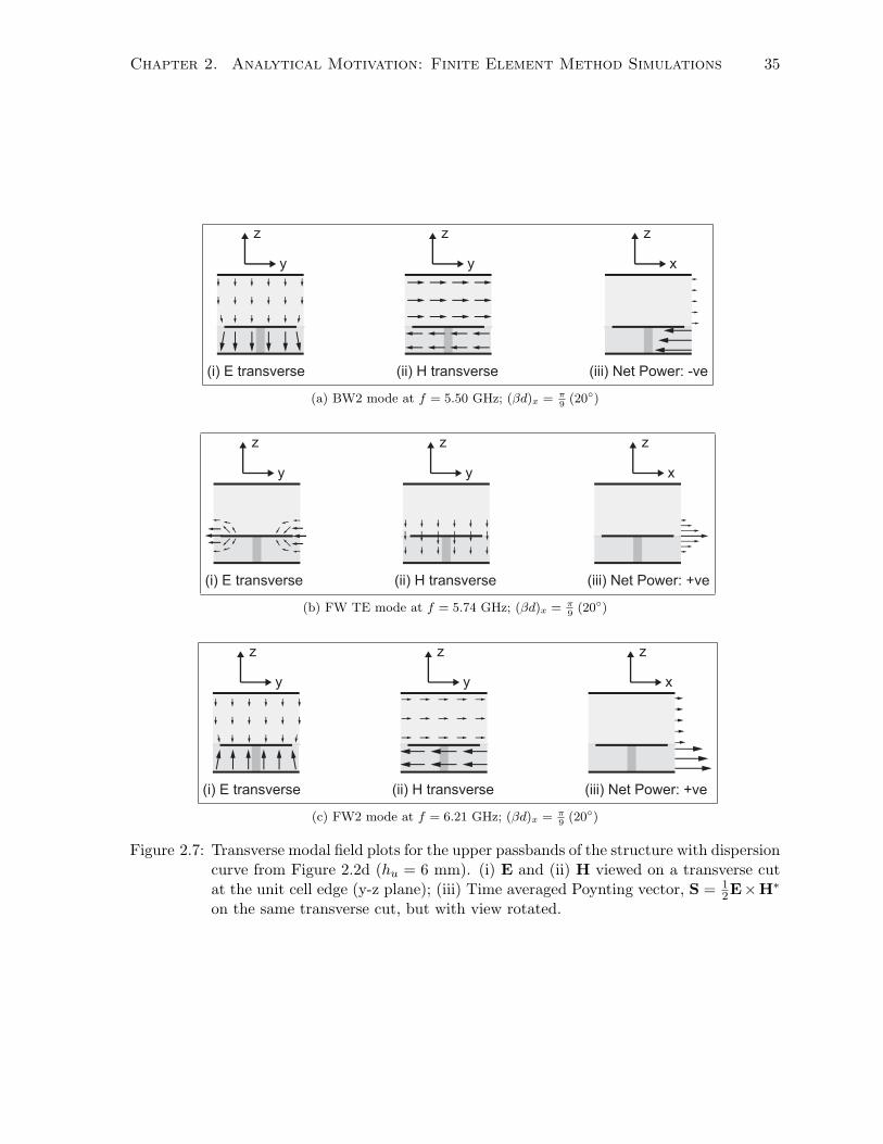
Chapter 2. Analytical Motivation: Finite Element Method Simulations 35
y
z
(i) E transverse
x
z
(ii) H transverse (iii) Net Power: -ve
y
z
(a) BW2 mode at f = 5.50 GHz; (βd)x = π9
(20)
y
z
(i) E transverse
x
z
(ii) H transverse (iii) Net Power: +ve
y
z
(b) FW TE mode at f = 5.74 GHz; (βd)x = π9
(20)
y
z
(i) E transverse
x
z
(ii) H transverse (iii) Net Power: +ve
y
z
(c) FW2 mode at f = 6.21 GHz; (βd)x = π9
(20)
Figure 2.7: Transverse modal field plots for the upper passbands of the structure with dispersioncurve from Figure 2.2d (hu = 6 mm). (i) E and (ii) H viewed on a transverse cutat the unit cell edge (y-z plane); (iii) Time averaged Poynting vector, S = 1
2E×H∗
on the same transverse cut, but with view rotated.
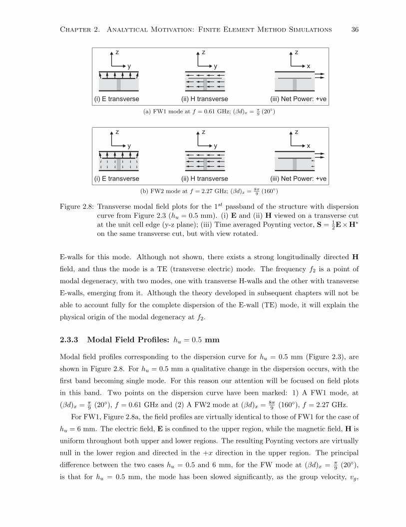
Chapter 2. Analytical Motivation: Finite Element Method Simulations 36
y
z
(i) E transverse
x
z
(ii) H transverse (iii) Net Power: +ve
y
z
(a) FW1 mode at f = 0.61 GHz; (βd)x = π9
(20)
y
z
(i) E transverse
x
z
(ii) H transverse (iii) Net Power: +ve
y
z
(b) FW2 mode at f = 2.27 GHz; (βd)x = 8π9
(160)
Figure 2.8: Transverse modal field plots for the 1st passband of the structure with dispersioncurve from Figure 2.3 (hu = 0.5 mm). (i) E and (ii) H viewed on a transverse cutat the unit cell edge (y-z plane); (iii) Time averaged Poynting vector, S = 1
2E×H∗
on the same transverse cut, but with view rotated.
E-walls for this mode. Although not shown, there exists a strong longitudinally directed H
field, and thus the mode is a TE (transverse electric) mode. The frequency f2 is a point of
modal degeneracy, with two modes, one with transverse H-walls and the other with transverse
E-walls, emerging from it. Although the theory developed in subsequent chapters will not be
able to account fully for the complete dispersion of the E-wall (TE) mode, it will explain the
physical origin of the modal degeneracy at f2.
2.3.3 Modal Field Profiles: hu = 0.5 mm
Modal field profiles corresponding to the dispersion curve for hu = 0.5 mm (Figure 2.3), are
shown in Figure 2.8. For hu = 0.5 mm a qualitative change in the dispersion occurs, with the
first band becoming single mode. For this reason our attention will be focused on field plots
in this band. Two points on the dispersion curve have been marked: 1) A FW1 mode, at
(βd)x = π9 (20), f = 0.61 GHz and (2) A FW2 mode at (βd)x = 8π
9 (160), f = 2.27 GHz.
For FW1, Figure 2.8a, the field profiles are virtually identical to those of FW1 for the case of
hu = 6 mm. The electric field, E is confined to the upper region, while the magnetic field, H is
uniform throughout both upper and lower regions. The resulting Poynting vectors are virtually
null in the lower region and directed in the +x direction in the upper region. The principal
difference between the two cases hu = 0.5 and 6 mm, for the FW mode at (βd)x = π9 (20),
is that for hu = 0.5 mm, the mode has been slowed significantly, as the group velocity, vg,

Chapter 2. Analytical Motivation: Finite Element Method Simulations 37
has been reduced substantially. This slowing effect will be examined and explained using the
developed theory in Chapter 5.
The point labeled FW2, Figure 2.8b, which occurs at (βd)x = 8π9 (160), will be compared
with BW1, Figure 2.4b (for hu = 6 mm), which also occurred at (βd)x = 8π9 (160). The
fields for FW2 are only slightly different from those of FW1, for the case hu = 0.5 mm. The
principal difference is that for FW2, a small oppositely polarized E has been generated in
the lower region. However significantly, the magnetic fields in both regions are nearly equal,
Hupper ≈ Hlower, unlike for BW1 (where hu = 6 mm). The fact that the magnetic field remains
nearly equal throughout both regions suggests that little displacement current is generated
along the longitudinally directed gaps, suppressing the BW mode in this case. The suppression
of the BW mode results in the structure losing its dual-mode character for relatively small huvalues. These observations will be addressed and explained in Chapters 4 and 5.
2.4 Summary
From the dispersion simulations the following points are noted. Disregarding the FW (TE) mode
emerging from f2, for the relatively large values of hu = 18 and 6 mm, the dispersion of the
shielded structure is seen to be a combination and deformation of the TL model BW dispersion
curve and the light line. For smaller values of hu, the lowest band dual-mode behaviour is
eliminated, and an identification of the dispersion as a combination of the two previously
mentioned curves becomes more difficult. It is interesting to note that the resonance frequencies
f3 and f4 remain invariant with respect to those of the TL model for any upper region height,
hu.
From the modal field profiles the following points are observed. All of the modes, excluding
those denoted by TE, are characterized by field strengths which are nearly uniform in each of
the two regions, upper and lower. The polarizations for these modes are such that the transverse
boundaries are acting as H-walls. However, in general for a given mode, the Poynting vectors
in the upper and lower regions are oppositely directed, so that the modes as a whole are
characterized as forward waves or backward waves by considering the net integrated power on
a transverse cross section.
The fact that the modes appear to be formed as the result of combinations of field excitations
in two distinct regions, with transverse H-wall boundary conditions, will be used as a motivation
for the analytical model developed in the following chapters. Using the developed analytical
model, the observations obtained from the FEM simulations will be re-examined and explained.
Chapter 3
Multiconductor transmission line
analysis: Building blocks
3.1 Introduction
In the previous chapter, FEM simulations for the shielded Sievenpiper structure were performed,
with both dispersion curves and modal field profiles examined. Several insights into the type of
model which could account for the observed dual-mode behaviour were obtained. The case of
on-axis propagation, (βd)y = 0 was examined, which was seen to be general enough to reveal
interesting dispersion and modal behaviour, yet it allows simplification in the development of
the analytical model to be initiated in this chapter and fully presented in the next chapter.
The key features of the dispersion curves were the dual-mode behaviour for relatively large
values of hu, with the dispersion curves in this case being formed from a slight perturbation
of the light line and the unshielded Sievenpiper TL model. Additionally, the peak of the first
stop-band occurred at a point away from the Brillouin zone center (βd = 0) or edge (βd = π).
The forward wave (FW) mode in the first band was seen to have strong upper region forward
direction power flow, and weak negative direction power flow in the lower region, with the
opposite being true for the backward wave (BW) mode. For the peak of the first band, the net
integrated power flow was zero.
For relatively small values of hu the dispersion curve within the first band became completely
single mode, and could seemingly no longer be identified with a slight perturbation of the light
line and the TL model curves. Significantly, the low frequency FW mode was severely slowed
down, while the BW band was completely eliminated. The modal power flow profiles in the first
band, which contained only a forward wave mode, had strong upper region forward direction
power flow, with minimal negative lower region power flow. Finally, the peak of the first band
occurred at the Brillouin zone edge, βd = π.
38
Chapter 3. Multiconductor analysis: Building Blocks 39
The field polarizations for all of the modes in the lowest band, and all, except one mode
in the upper bands, were seen to correspond to H-walls on the transverse boundaries. For the
lone upper band mode referred to above, which did not correspond to transverse H-walls, the
field polarization on the transverse boundary was an E-wall.
In this chapter, and the next, some of the features described above will be used initially to aid
in the development of the proposed model, and subsequently will be explained with the derived
analytical model. It will be demonstrated that wave propagation of the shielded structure can
be analyzed using multiconductor transmission line (MTL) theory. In the remainder of this
chapter the following points will be addressed. Standard MTL theory describes propagation for
systems which are uniform along the propagation direction. However, the MTL model of the
shielded structure will be shown to correspond to a periodic (and hence non-uniform along the
direction of propagation) MTL geometry. In order to understand the propagation in the actual
structure, which is periodically loaded, it will be useful to define and analyze the propagation
properties of the underlying unloaded MTL geometry, which is one of the building blocks in
the fully loaded periodic model. It will be determined that for the defined underlying unloaded
geometry, two independent modes of propagation, which correspond essentially to plane waves
propagating in the upper and lower regions of the structure, are supported. Both the dispersion
curves and modal field profiles of the unloaded MTL geometry will be analyzed. That these
modes form a basis to describe wave propagation in the actual shielded structure is anticipated
due to the field profiles observed in the previous chapter.
Subsequently, the determination of the loading elements, which alter the propagation prop-
erties of the unloaded geometry, will be undertaken. The gaps along the direction of propagation
will be shown to correspond to equivalent series capacitances, C, while the vias between the
patch layer and ground will be shown to correspond to equivalent shunt inductances, L. Typ-
ically the loading elements are calculated by considering appropriate scattering simulations,
which usually involve two-port configurations. However, due to the presence of the top shield-
ing conductor, a simple two-port scattering analysis will be shown to be insufficient in the
calculation of C, and a more thorough four-port scattering analysis will be shown to be neces-
sary, especially in the case where hu is relatively small. The calculation of L will proceed in a
similar manner.
This analysis will subsequently be used in the next chapter to characterize the propagation
properties of the actual periodic geometry of the shielded structure, with dispersion curves,
modal field profiles, and important resonant frequencies derived and explained.
Chapter 3. Multiconductor analysis: Building Blocks 40
3.2 Unloaded MTL Geometry
In correspondence with the FEM simulations of the previous chapter, on-axis propagation of
the shielded structure, with (βd)y = 0 will be examined. It was observed that for the lowest
band and most of the upper bands, the transverse boundaries were characterized by H-walls.
Initially, the assumption of transverse H-walls will be made, although later it will be shown that
(βd)y = 0 implies that the transverse boundaries are either H-walls or E-walls for symmetric
structures. In fact, a stronger condition will be shown to be true in Chapter 4: due to symmetry,
the condition (βd)y = 0 implies that the central bisecting plane of the unit cell has the same
boundary condition as the edge walls.
The present section will focus on defining and then analyzing propagation in the unloaded
MTL geometry, which will be a key building block in the analysis of the shielded structure.
The simplest way to introduce the unloaded geometry, though, will be to show the transfor-
mation which takes the unloaded structure into the actual loaded (shielded) structure. This
transformation is depicted in Figure 3.1. The unloaded geometry is depicted from a side view,
Figure 3.1a and a top view, Figure 3.1c, where the top view is taken just below the upper
shielding plane. The unloaded geometry is seen to be an infinite (along x) array of strips,
placed between the upper shielding conductor and the ground plane. The direction of propa-
gation is assumed to be along x, and hence waves propagating along the length of the infinite
strips do not experience any discontinuities. The side boundaries (dashed lines) are assumed
to be H-walls. Figures 3.1b and d depict the transformed, loaded geometry, which is seen to be
generated by periodically cutting, along y, gaps in the infinite strips, thereby creating islands
of patches and simultaneously placing vias from the center of each patch to the ground plane.
The gaps and the vias provide discontinuities to waves propagating along x, and thus will be
referred to as the loading elements.
In Figure 3.2 a system of n+1 parallel conductors is depicted, with conductor 0 taken as the
reference conductor. The system is assumed uniform along the x axis. Such a system represents
a generic multiconductor transmission line (MTL) geometry, and the lowest order modes of such
a configuration are quasi-TEM in general (purely TEM if the surrounding dielectric medium is
uniform) [32]. A transverse cut of the unloaded geometry for the specific case of the shielded
Sievenpiper structure is shown in Figure 3.3. The upper shielding conductor is labeled 1, the
patch layer conductor is labeled 2, and the ground plane is left unlabeled. Thus the unloaded
shielded Sievenpiper structure is a 2 + 1 conductor MTL geometry with n = 2. Returning to
the generic MTL geometry shown in Figure 3.2, under the assumption that the currents on the
conductors are purely longitudinal (along x) the resulting magnetic fields are purely transverse.
One is then able to uniquely define the voltage on the p− th conductor with respect to ground

Chapter 3. Multiconductor analysis: Building Blocks 41
Side view; dashed lines represent H walls
Viewed looking down (-z), below the top (shielding) plane
z
x
y
y
(a) Unloaded (b) Loaded
(c) Unloaded (d) Loaded
Figure 3.1: Transformation of an infinite 1-D periodic array of strips, (a) and (c), into an infinite2-D periodic array of isolated patches (b) and (d). Vias connected from the centerof each patch to ground for (b) and (d). The transverse boundary conditions areassumed to be H-walls for the case of on-axis propagation in the MTL model.
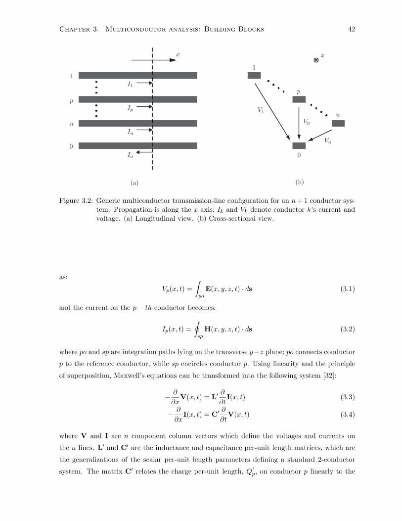
Chapter 3. Multiconductor analysis: Building Blocks 42
xx
11
p
p
n
n
00
I1
Ip
In
Io
V1
Vp
Vn
(a) (b)
Figure 3.2: Generic multiconductor transmission-line configuration for an n+ 1 conductor sys-tem. Propagation is along the x axis; Ik and Vk denote conductor k’s current andvoltage. (a) Longitudinal view. (b) Cross-sectional view.
as:
Vp(x, t) =∫po
E(x, y, z, t) · ds (3.1)
and the current on the p− th conductor becomes:
Ip(x, t) =∮sp
H(x, y, z, t) · ds (3.2)
where po and sp are integration paths lying on the transverse y−z plane; po connects conductor
p to the reference conductor, while sp encircles conductor p. Using linearity and the principle
of superposition, Maxwell’s equations can be transformed into the following system [32]:
− ∂
∂xV(x, t) = L′
∂
∂tI(x, t) (3.3)
− ∂
∂xI(x, t) = C′
∂
∂tV(x, t) (3.4)
where V and I are n component column vectors which define the voltages and currents on
the n lines. L′ and C′ are the inductance and capacitance per-unit length matrices, which are
the generalizations of the scalar per-unit length parameters defining a standard 2-conductor
system. The matrix C′ relates the charge per-unit length, Q′p, on conductor p linearly to the

Chapter 3. Multiconductor analysis: Building Blocks 43
y
z
hu
hl
ǫ1
ǫ2
w
d
Conductor 1; V1, I1
Conductor 2; V2, I2
Ground
Figure 3.3: Parameters defining the unloaded MTL geometry for on-axis propagation assumingtransverse H-walls (dashed lines). Conductors 1 and 2 have voltages, V1, V2,defined with respect to ground, along with currents I1, I2, which are used todefine the per-unit-length capacitance and inductance matrices, C
′and L
′.
voltages, Vj on all of the other conductors:
Q′p =
n∑j=1
C′pjVj (3.5)
or in matrix form:
Q′ = C′V (3.6)
where Q′ is an n component column vector containing the charge per-unit-lengths on conductors
1 through n. The matrix, L′ relates the per-unit length flux, Ψ′p, linking conductor p to the
ground conductor, linearly to the currents, Ij on all of the other conductors:
Ψ′p =
n∑j=1
L′pjIj (3.7)
or in matrix form:
Ψ′ = L′I (3.8)
where Ψ′ is an n component column flux linkage vector.
Under the assumption that the fields are time harmonic, with angular frequency ω the
equations (3.3) and (3.4) reduce to:
− d
dxV(x) = jωL′ I(x) (3.9)
− d
dxI(x) = jωC′V(x) (3.10)
where the longitudinal impedance matrix, Z′ , and the transverse admittance matrix, Y′, are

Chapter 3. Multiconductor analysis: Building Blocks 44
y
z
huhu
hlhl
dd
V1
V2 = 0
I1
I2 = 0
(a) C′11
(b) L′11
Figure 3.4: Boundary value problems used to determine C′11 and L
′11.
defined by Z′ = jωL′ and Y′ = jωC′. For an unloaded 2 + 1 conductor system such as that
considered here, C′ and L′ are given explicitly by:[Q′1
Q′2
]= C′
[V1
V2
]=
[C′11 C
′12
C′21 C
′22
][V1
V2
](3.11)
and [Ψ′1
Ψ′2
]= L′
[I1
I2
]=
[L′11 L
′12
L′21 L
′22
][I1
I2
](3.12)
The components of C′ and L′ are obtained by solving a set of boundary value problems. For
example the C′11 is obtained by solving the following electrostatic boundary value problem:
C′11 =
Q′1
V1; V2 = 0 (3.13)
while L′11 is obtained by solving the following magnetostatic problem:
L′11 =
Ψ′1
I1; I2 = 0. (3.14)
The approximate field structures which are obtained in the solutions of these two problems
are depicted in Figure 3.4. Assuming that the plate width, w is approximately equal to the
periodicity so that, w ≈ d, it is anticipated that the fields will be approximately those of a
multiple parallel-plate geometry. Due to the presence of an H-wall at the transverse boundary
the fringing fields are assumed to be small. With these approximations it can be shown that
C′11 =
ε1weffhu
, where weff = w + ∆w is the effective width which is used to account for the
fringing fields, and∆ww 1 is small. The remaining components of C′ may be similarly
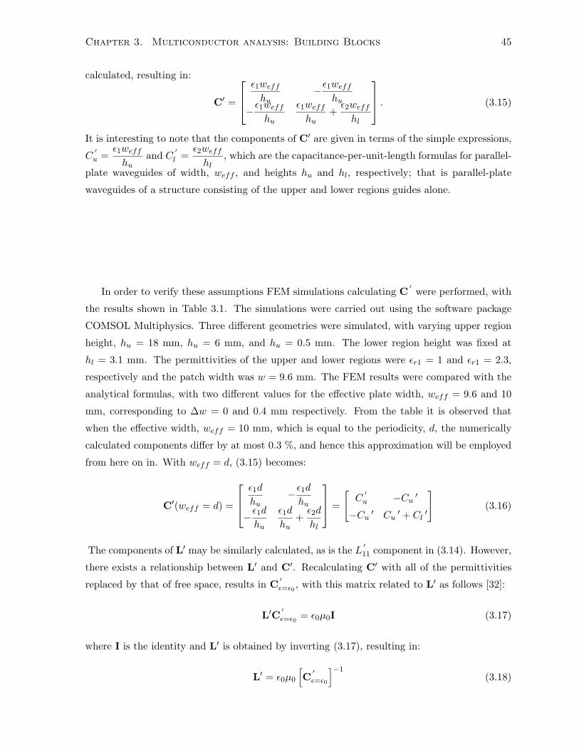
Chapter 3. Multiconductor analysis: Building Blocks 45
calculated, resulting in:
C′ =
ε1weffhu
−ε1weffhu
−ε1weffhu
ε1weffhu
+ε2weffhl
. (3.15)
It is interesting to note that the components of C′ are given in terms of the simple expressions,
C′u =
ε1weffhu
and C′l =
ε2weffhl
, which are the capacitance-per-unit-length formulas for parallel-
plate waveguides of width, weff , and heights hu and hl, respectively; that is parallel-plate
waveguides of a structure consisting of the upper and lower regions guides alone.
In order to verify these assumptions FEM simulations calculating C′
were performed, with
the results shown in Table 3.1. The simulations were carried out using the software package
COMSOL Multiphysics. Three different geometries were simulated, with varying upper region
height, hu = 18 mm, hu = 6 mm, and hu = 0.5 mm. The lower region height was fixed at
hl = 3.1 mm. The permittivities of the upper and lower regions were εr1 = 1 and εr1 = 2.3,
respectively and the patch width was w = 9.6 mm. The FEM results were compared with the
analytical formulas, with two different values for the effective plate width, weff = 9.6 and 10
mm, corresponding to ∆w = 0 and 0.4 mm respectively. From the table it is observed that
when the effective width, weff = 10 mm, which is equal to the periodicity, d, the numerically
calculated components differ by at most 0.3 %, and hence this approximation will be employed
from here on in. With weff = d, (3.15) becomes:
C′(weff = d) =
ε1d
hu−ε1dhu
−ε1dhu
ε1d
hu+ε2d
hl
=
[C′u −Cu ′
−Cu ′ Cu′ + Cl
′
](3.16)
The components of L′ may be similarly calculated, as is the L′11 component in (3.14). However,
there exists a relationship between L′ and C′. Recalculating C′ with all of the permittivities
replaced by that of free space, results in C′ε=ε0 , with this matrix related to L′ as follows [32]:
L′C′ε=ε0 = ε0µ0I (3.17)
where I is the identity and L′ is obtained by inverting (3.17), resulting in:
L′ = ε0µ0
[C′ε=ε0
]−1(3.18)

Chapter 3. Multiconductor analysis: Building Blocks 46
Table 3.1: Comparison of the numerical (FEM) and analytic C′ (capacitance) matrices for: (a)hu = 18 mm, (b) hu = 6, (c) hu = 0.5 mm. The analytic C′ matrix is calculated fortwo different values of the effective width, weff = 10.0 and 9.6 mm.
(a) hu = 18mm
Capacitance matrix components(pFm
)C′11 C
′12 C
′21 C
′22
FEM 4.92 -4.91 -4.91 70.51analytic (weff = 10 mm) 4.92 -4.92 -4.92 70.58
% difference (FEM & weff = 10 mm) 0 0.2 0.2 0.3analytic (weff = 9.6 mm) 4.72 -4.72 -4.72 67.75
% difference (FEM & weff = 9.6 mm) 3.5 3.8 3.8 4.2
(b) hu = 6mm
Capacitance matrix components(pFm
)C′11 C
′12 C
′21 C
′22
FEM 14.75 -14.73 -14.73 80.32analytic (weff = 10 mm) 14.75 -14.75 -14.75 80.41
% difference (FEM & weff = 10 mm) 0 0.2 0.2 0.3analytic (weff = 9.6 mm) 14.16 -14.16 -14.16 77.19
% difference (FEM & weff = 9.6 mm) 3.5 3.8 3.8 4.2
(c) hu = 0.5mm
Capacitance matrix components(pFm
)C′11 C
′12 C
′21 C
′22
FEM 176.45 -176.21 -176.21 241.58analytic (weff = 10 mm) 177.0 -177.0 -177.0 242.7
% difference (FEM & weff = 10 mm) 0 0.2 0.2 0.3analytic (weff = 9.6 mm) 169.9 -169.9 -169.9 233.0
% difference (FEM & weff = 9.6 mm) 3.5 3.8 3.8 4.2
Chapter 3. Multiconductor analysis: Building Blocks 47
Using (3.16) and (3.18) results in:
L′ =
µohld +µohud
µohld
µohld
µohld
=
[L′l + L′u L′l
L′l L′l
](3.19)
where the components of L′, L′u =µohud
and L′l =µohld
are again related to those of parallel-
plate guides composed of the upper and lower regions alone. Thus the components of both C′
and L′ are given in terms of simple expressions involving parallel-plate geometries when w ≈ d.
When w is significantly less than d these expressions will not be valid and the evaluation of C′
will require a numerical solution.
Having obtained expressions for C′ and L′ the system of equations (3.9) and (3.10) may be
solved. Expanding these equations results in:
−dV1
dx= Z1I1 + ZmI2 (3.20)
−dV2
dx= ZmI1 + ZmI2 (3.21)
−dI1dx
= Y1V1 + YmV2 (3.22)
−dI2dx
= YmV1 + Y2V2 (3.23)
The above first order system of equation can be transformed into a second order system involving
only the voltages by eliminating the current in (3.20) through (3.23) resulting in:
d2V1
dx2− a1V1 − b1V2 = 0 (3.24)
d2V2
dx2− a2V2 − b2V1 = 0 (3.25)
Solving for V2 in (3.24) and inserting it into (3.25), the above coupled system of equations is
reduced to an ordinary differential equation:
d4V1
dx4− (a1 + a2)
d2V1
dx2+ (a1a2 − b1b2)V1 = 0 (3.26)

Chapter 3. Multiconductor analysis: Building Blocks 48
with a similar equation for V2. The coefficients are evaluated to be:
a1 = Y1Z1 + YmZm = −ω2C′uL′u (3.27)
a2 = Y2Z2 + YmZm = −ω2C′l L′l (3.28)
b1 = Z1Ym + Y2Zm = −ω2(C′l L′l − C
′uL′u) (3.29)
b2 = Z2Ym + Y1Zm = 0 (3.30)
Assuming solutions of the form Voe−γz for V1 and V2, the eigenvalue equation for (3.26) is
obtained:
γ4 + (−a1 − a2) γ2 + (a1a2 − b1b2) = 0 (3.31)
which is quadratic equation in γ2, with solutions
γ2a,b =
a1 + a2
2±√
(a1 + a2)2 − 4(a1a2 − b1b2)2
(3.32)
The solutions of (3.32) represent two independent modes, propagating in the positive and
negative directions:
γ1,2 = ±γa and γ3,4 = ±γb (3.33)
Substituting (3.27) through (3.30) into (3.32) yields the propagation constants in term of the
MTL parameters:
γa = jω√L′lC′l (3.34)
γb = jω√L′uC
′u (3.35)
The two solutions (3.34) and (3.35) represent purely propagating dispersion-free modes, with
phase velocities, vl = 1qL′lC′l
and vu = 1√L′uC
′u
completely determined by the electrical properties
of the upper and lower regions alone, and which are independent of the heights of the lower
and upper regions. Dispersion curves for the two modes obtained using MTL analysis are
compared with FEM simulated results in Figure 3.5, which confirm that the two independent
modes are indeed virtually dispersion free, and match well the FEM simulated results. The
modal eigenvectors, corresponding to the propagation constants are given by:V1
V2
I1
I2
=
1
Ra
Ya1
RaYa2
Vo and
V1
V2
I1
I2
=
1
Rb
Yb1
RbYb2
Vo (3.36)
Chapter 3. Multiconductor analysis: Building Blocks 49
where Ra and Rb represent the ratio of the voltages on the two conductors. From (3.24) and
(3.25) the ratios are determined to be:
Ra,b =V2
V1=γ2a,b − a1
b1(3.37)
The characteristic admittances for conductors 1 and 2, Ya1 and Ya2, are given by:
Ya1 = γaZ2 − ZmRaZ1Z2 − Z2
m
(3.38)
Ya2 =γaRa
Z1Rc − ZmZ1Z2 − Z2
m
(3.39)
with similar formulas for Yb1 and Yb2. Substituting the relevant terms for the geometry under
consideration the modal eigenvectors are given by:
γa = jω√L′lC′l ⇒
V1
V2
I1
I2
=
1
1
01Zl
Vo and γb = jω√L′uC
′u ⇒
V1
V2
I1
I2
=
1
01Zu
− 1Zu
Vo (3.40)
where Zu =√
L′uC ′u
and Zl =√
L′l
C′l
are the characteristic impedances of parallel-plate waveguides
consisting of the upper and lower regions alone. The eigenvectors for the negative traveling
waves, −γa,b are identical, except that the current components are negative of those in (3.40).
It is recalled that the components of the matrices C′ and L′ were derived analytically under
the assumption of parallel-plate type fields with minor fringing, and that these were verified
numerically. Under these assumptions the upper region the electric field, Eu is proportional
to (V1 − V2), while in the lower region, the electric field, El is proportional to (V2 − 0). For
the magnetic fields, the upper region magnetic field, Hu is proportional to I1, while the lower
region magnetic field, Hl is proportional to I1 + I2.
For the eigenvector corresponding to γa = jω√L′lC′l it is seen that V1 − V2 = Vo − Vo = 0,
while V2 − 0 = Vo − 0, and hence E is confined to the lower region ( El 6= 0 and Eu = 0). The
magnetic field in the upper region is proportional to I1 = 0, and hence zero, while in the lower
region the magnetic field is non-zero as I1 + I2 = VoZl
(Hl 6= 0 and Hu = 0). In a similar manner
it can be shown that for the mode corresponding to γb = jω√L′uC
′u, the upper region fields
are non-zero, Eu 6= 0, Hu 6= 0, while the lower region fields are zero, El = 0, Hl = 0. Modal
field plots obtained from FEM simulations depicting E confirm these conclusions as shown in
Figure 3.6. Each of the two modes are confined to one of the lower or upper regions, with
minimal fringing into the other region. This is consistent with the fact that the propagation
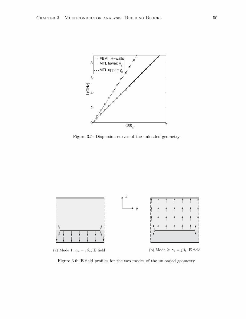
Chapter 3. Multiconductor analysis: Building Blocks 50
0
2
4
6
8
π(βd)x
f (G
Hz)
FEM: H−wallsMTL lower: γ
a
MTL upper: γb
Figure 3.5: Dispersion curves of the unloaded geometry.
y
z
(a) Mode 1: γa = jβa; E field (b) Mode 2: γb = jβb; E field
Figure 3.6: E field profiles for the two modes of the unloaded geometry.

Chapter 3. Multiconductor analysis: Building Blocks 51
P1+,− P2−
TLTL
Radiation to free space
Figure 3.7: Two-port scattering setup used to determine the series capacitance, C.
constants of each of the modes depends only on the electrical properties of one region and are
independent of the other.
3.3 Determination of loading elements
Without the presence of the top shielding conductor, a two-port full wave scattering simulation
would be sufficient to calculate the equivalent series capacitance, C, due to the gap, and the
equivalent shunt inductance, L, due to the via. The depiction of such a scenario for the
determination of C is shown in Figure 3.7. The transmission lines, labeled TL on either side of
the gap are simply the geometry of the lower region of the shielded structure, with transverse
H-walls. At each port only a single quasi-TEM mode, which is essentially the parallel-plate
mode of the lower region, is considered. By performing a full wave simulation and then de-
embedding the two-port scattering parameters to the location of the discontinuity, C may be
calculated.
However, in attempting this, two problems arise. First, for the situation depicted in Fig-
ure 3.7, the calculated equivalent capacitance, C will consist of both a real part (the capaci-
tance), and an imaginary part, which is due to radiation leakage into free space. Figure 3.8
shows the results for a two port scattering simulation used to determine C. The real part of
C is approximately 0.28 pF from 1 to 7 GHz and then increases and finally dips slightly at 10
GHz. The imaginary part of C is non-zero and represents a radiation leakage component. The
shielded structure is a closed geometry, and therefore no energy can be lost to free space. Thus,
the values of C obtained for the shielded structure should be purely real. Although the values
of C obtained using the TL setup of Figure 3.7 consist of both real and imaginary parts, one
might assume that by taking the real part of this number, a reasonable approximation to the
actual value of C for the shielded structure could be obtained. The second problem encountered
with this approach is as follows. In comparing the dispersion curves of the shielded structure
obtained using MTL analysis (to be shown in the next chapter), which incorporate C values
obtained as above, and the FEM generated dispersion curves, it was observed that the two sets
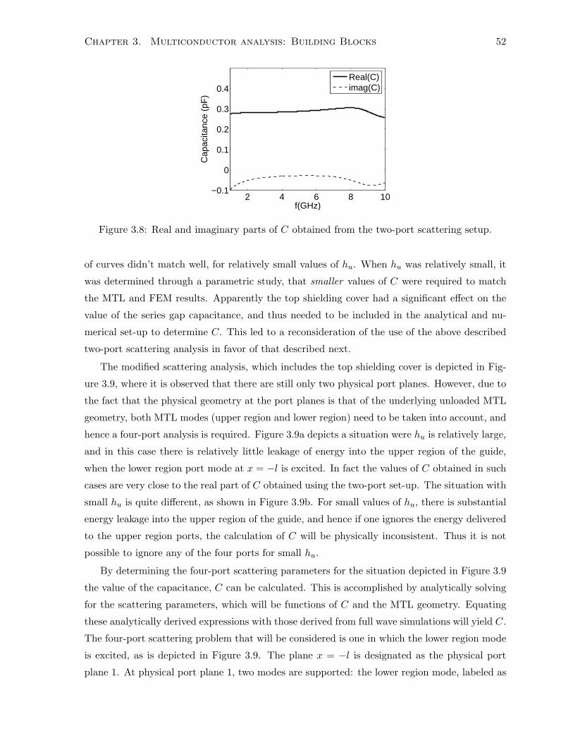
Chapter 3. Multiconductor analysis: Building Blocks 52
2 4 6 8 10−0.1
0
0.1
0.2
0.3
0.4
f(GHz)C
apac
itanc
e (p
F)
Real(C)imag(C)
Figure 3.8: Real and imaginary parts of C obtained from the two-port scattering setup.
of curves didn’t match well, for relatively small values of hu. When hu was relatively small, it
was determined through a parametric study, that smaller values of C were required to match
the MTL and FEM results. Apparently the top shielding cover had a significant effect on the
value of the series gap capacitance, and thus needed to be included in the analytical and nu-
merical set-up to determine C. This led to a reconsideration of the use of the above described
two-port scattering analysis in favor of that described next.
The modified scattering analysis, which includes the top shielding cover is depicted in Fig-
ure 3.9, where it is observed that there are still only two physical port planes. However, due to
the fact that the physical geometry at the port planes is that of the underlying unloaded MTL
geometry, both MTL modes (upper region and lower region) need to be taken into account, and
hence a four-port analysis is required. Figure 3.9a depicts a situation were hu is relatively large,
and in this case there is relatively little leakage of energy into the upper region of the guide,
when the lower region port mode at x = −l is excited. In fact the values of C obtained in such
cases are very close to the real part of C obtained using the two-port set-up. The situation with
small hu is quite different, as shown in Figure 3.9b. For small values of hu, there is substantial
energy leakage into the upper region of the guide, and hence if one ignores the energy delivered
to the upper region ports, the calculation of C will be physically inconsistent. Thus it is not
possible to ignore any of the four ports for small hu.
By determining the four-port scattering parameters for the situation depicted in Figure 3.9
the value of the capacitance, C can be calculated. This is accomplished by analytically solving
for the scattering parameters, which will be functions of C and the MTL geometry. Equating
these analytically derived expressions with those derived from full wave simulations will yield C.
The four-port scattering problem that will be considered is one in which the lower region mode
is excited, as is depicted in Figure 3.9. The plane x = −l is designated as the physical port
plane 1. At physical port plane 1, two modes are supported: the lower region mode, labeled as

Chapter 3. Multiconductor analysis: Building Blocks 53
M1+,−
M2−
M3−
M4−
MTL(l)MTL(l)
Physicalport plane 1:
x = −l
Physicalport plane 2:
x = l0− 0+
(a) Large hu: Small energy leakage to upper region
M1+,−
M2−
M3−
M4−
MTL(l)MTL(l)
Physicalport plane 1:
x = −l
Physicalport plane 2:
x = l0− 0+
(b) Small hu: Large energy leakage to upper region
Figure 3.9: Four-port scattering setup used to determine the series capacitance, C, depictedfor (a) large hu and (b) small hu. For a lower region excitation a larger quantity ofenergy leaks to the upper region when hu is small.

Chapter 3. Multiconductor analysis: Building Blocks 54
M1 and the upper region mode, labeled as M2. The plane x = l is designated as the physical
port plane 2, which also supports two modes: the lower region mode labeled as M3 and the
upper region mode labeled as M4.
For the situation considered in Figure 3.9 the lower region mode, M1 at x = −l is excited,
with the other three modes, M2, M3, and M4 matched. The quantities describing each of
the port modes M1, M2, M3, and M4 are given by 2 component voltage and current column
vectors. These column vectors are simply the lower region (M1 and M3) and upper region (M2
and M4) eigenvectors, as given in (3.40). The total mode 1 voltage and current vectors, VM1
and IM1 are comprised of incident, +, and reflected, − components as given by:
VM1 = V +M1 + V −
M1 IM1 = I +M1 + I −M1 (3.41)
where V +M1 =
[1
1
]V +M1 , I +
M1 =
01Zl
V +M1 , and V −
M1 =
[1
1
]V −M1 , I −M1 =
0
− 1Zl
V −M1 . The
scalar variables V +M1 and V −
M1 are incident and reflected amplitudes. The upper region mode
at x = −l, M2 is matched, so that only a reflected component is present. Thus the total mode
2 voltage and current vectors VM2 and IM2 are given by:
VM2 = V −M2 IM2 = I −M2 (3.42)
where VM2 =
[1
0
]V −M2 , and I −M2 =
− 1Zu1Zu
V −M2 . The total voltage, V(x=−l) = V −
M1 + V +M1 +
V −M2, and current, I(x=−l) = I −M1 + I +
M1 + I −M2, at physical port plane 1 is given in component
form as: V1
V2
I1
I2
(x=−l)
=
V +M1 + V −
M1 + V −M2
V +M1 + V −
M1
−V−
M2
ZuV +M1
Zl− V −
M1
Zl+V −M2
Zu
(3.43)
For the physical port plane 2 at x = l only the reflected lower and upper region modes are
present, with amplitudes, V −M3 and V −
M4 , respectively. The total voltage, V(x=l) = V −M3+V −
M4,

Chapter 3. Multiconductor analysis: Building Blocks 55
and current I(x=l) = I −M3 + I −M4 is given in component form as:
V1
V2
I1
I2
(x=l)
=
V −M3 + V −
M4
V −M3
V −M4
ZuV −M3
Zl− V −
M4
Zu
(3.44)
The transfer matrix, TC , which relates the voltage and current across the series capacitance,
C is given by: V1(0−)
V2(0−)
I1(0−)
I2(0−)
= TC
V1(0+)
V2(0+)
I1(0+)
I2(0+)
=
1 0 0 0
0 1 0 ZC
0 0 1 0
0 0 0 1
V1(0+)
V2(0+)
I1(0+)
I2(0+)
(3.45)
where ZC = 1jωC .
After the numerical simulation is performed, the reference planes used to calculate the S
parameters are transferred just to the right and the left of the discontinuity, with the original
port 1 reference plane de-embedded from x = −l→ x = 0−, while the port 2 reference plane is
de-embedded from x = l → x = 0+. With the new reference planes defined as such, the total
voltage and current definitions at x = −l and x = l may be substituted into (3.45), and the
resulting linear system of equations can be solved for the multiport scattering parameters. Due
to the fact that the impedances, Zl and Zu of lower and upper modes are not equal, generalized
scattering parameters are needed, which are defined by:
Sij =V −i√Zj
V +j
√Zi
∣∣∣∣∣V +k =0 for k 6=j
(3.46)
By solving the linear system obtained from (3.45) the generalized scattering parameters are
found and given by:
S11 =V −M1
V +M1
=Zu
Zl + 2jωCZlZu + Zu(3.47)
S21 =V −M2
V +M1
√ZlZu
= − ZuZl + 2jωCZlZu + Zu
√ZlZu
(3.48)
S31 =V −M3
V +M1
=(2ωCZu − j)Zlj
Zl + 2jωCZlZu + Zu(3.49)
S41 =V −M4
V +M1
√ZlZu
=Zu
Zl + 2jωCZlZu + Zu
√ZlZu
(3.50)
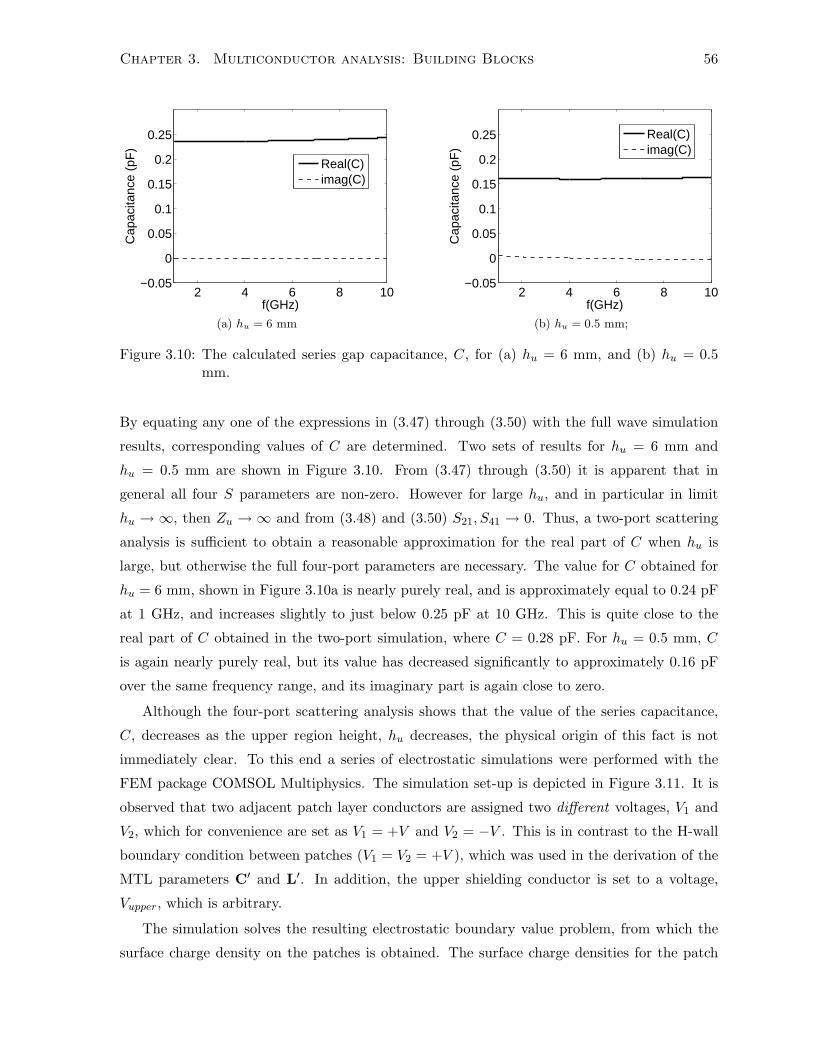
Chapter 3. Multiconductor analysis: Building Blocks 56
2 4 6 8 10−0.05
0
0.05
0.1
0.15
0.2
0.25
f(GHz)
Cap
acita
nce
(pF
)
Real(C)imag(C)
(a) hu = 6 mm
2 4 6 8 10−0.05
0
0.05
0.1
0.15
0.2
0.25
f(GHz)
Cap
acita
nce
(pF
)
Real(C)imag(C)
(b) hu = 0.5 mm;
Figure 3.10: The calculated series gap capacitance, C, for (a) hu = 6 mm, and (b) hu = 0.5mm.
By equating any one of the expressions in (3.47) through (3.50) with the full wave simulation
results, corresponding values of C are determined. Two sets of results for hu = 6 mm and
hu = 0.5 mm are shown in Figure 3.10. From (3.47) through (3.50) it is apparent that in
general all four S parameters are non-zero. However for large hu, and in particular in limit
hu → ∞, then Zu → ∞ and from (3.48) and (3.50) S21, S41 → 0. Thus, a two-port scattering
analysis is sufficient to obtain a reasonable approximation for the real part of C when hu is
large, but otherwise the full four-port parameters are necessary. The value for C obtained for
hu = 6 mm, shown in Figure 3.10a is nearly purely real, and is approximately equal to 0.24 pF
at 1 GHz, and increases slightly to just below 0.25 pF at 10 GHz. This is quite close to the
real part of C obtained in the two-port simulation, where C = 0.28 pF. For hu = 0.5 mm, C
is again nearly purely real, but its value has decreased significantly to approximately 0.16 pF
over the same frequency range, and its imaginary part is again close to zero.
Although the four-port scattering analysis shows that the value of the series capacitance,
C, decreases as the upper region height, hu decreases, the physical origin of this fact is not
immediately clear. To this end a series of electrostatic simulations were performed with the
FEM package COMSOL Multiphysics. The simulation set-up is depicted in Figure 3.11. It is
observed that two adjacent patch layer conductors are assigned two different voltages, V1 and
V2, which for convenience are set as V1 = +V and V2 = −V . This is in contrast to the H-wall
boundary condition between patches (V1 = V2 = +V ), which was used in the derivation of the
MTL parameters C′ and L′. In addition, the upper shielding conductor is set to a voltage,
Vupper, which is arbitrary.
The simulation solves the resulting electrostatic boundary value problem, from which the
surface charge density on the patches is obtained. The surface charge densities for the patch
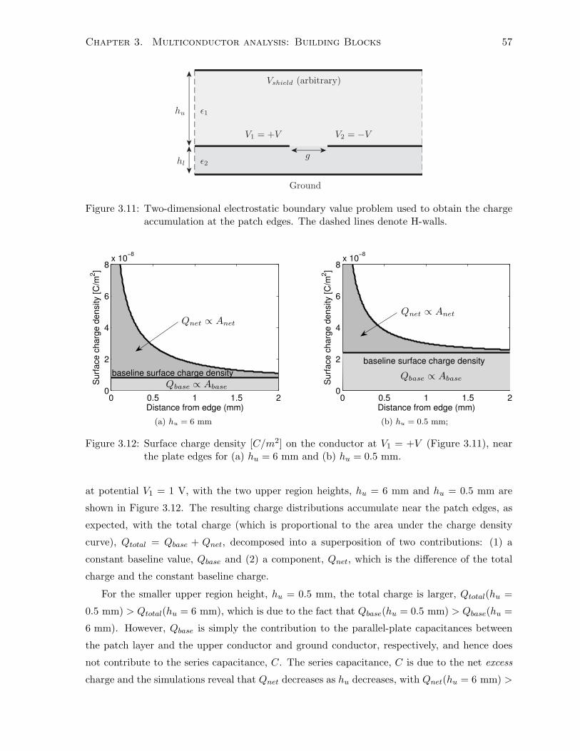
Chapter 3. Multiconductor analysis: Building Blocks 57
hu
hl
ǫ1
ǫ2
V1 = +V V2 = −V
Vshield (arbitrary)
Ground
g
Figure 3.11: Two-dimensional electrostatic boundary value problem used to obtain the chargeaccumulation at the patch edges. The dashed lines denote H-walls.
(a) hu = 6 mm (b) hu = 0.5 mm;
Figure 3.12: Surface charge density [C/m2] on the conductor at V1 = +V (Figure 3.11), nearthe plate edges for (a) hu = 6 mm and (b) hu = 0.5 mm.
at potential V1 = 1 V, with the two upper region heights, hu = 6 mm and hu = 0.5 mm are
shown in Figure 3.12. The resulting charge distributions accumulate near the patch edges, as
expected, with the total charge (which is proportional to the area under the charge density
curve), Qtotal = Qbase + Qnet, decomposed into a superposition of two contributions: (1) a
constant baseline value, Qbase and (2) a component, Qnet, which is the difference of the total
charge and the constant baseline charge.
For the smaller upper region height, hu = 0.5 mm, the total charge is larger, Qtotal(hu =
0.5 mm) > Qtotal(hu = 6 mm), which is due to the fact that Qbase(hu = 0.5 mm) > Qbase(hu =
6 mm). However, Qbase is simply the contribution to the parallel-plate capacitances between
the patch layer and the upper conductor and ground conductor, respectively, and hence does
not contribute to the series capacitance, C. The series capacitance, C is due to the net excess
charge and the simulations reveal that Qnet decreases as hu decreases, with Qnet(hu = 6 mm) >

Chapter 3. Multiconductor analysis: Building Blocks 58
(a) hu = 6 mm (b) hu = 0.5 mm;
Figure 3.13: Streamline plots of the electric field for (a) hu = 6 mm and (b) hu = 0.5 mm.
Qnet(hu = 0.5 mm). The series capacitance, C is given by C = QnetV1−V2
and hence C decreases
as hu decreases. The excess charge accumulation is due to the potential difference between the
patches, but as the upper region height decreases a larger density of field lines which begin on
one patch will terminate on the shielding conductor rather than the adjacent patch, as seen in
Figure 3.13, resulting in reduced series capacitance as hu decreases.
The determination of the equivalent via inductance, L as depicted in Figure 3.14 proceeded
in a similar manner to that for C, with a four-port scattering setup. The calculation of the
four-port scattering parameters for the equivalent via inductance resulted in:
S11 =V −M1
V +M1
=−jZl
Zlj − 2ωL(3.51)
S21 =V −M2
V +M1
√ZlZu
= 0 (3.52)
S31 =V −M3
V +M1
= − 2ωLZlj − 2ωL
(3.53)
S41 =V −M4
V +M1
√ZlZu
= 0 (3.54)
from which it is apparent that when a lower region port is excited, there is no energy leakage to
the upper region, and hence L is not dependent on the upper region height, hu, unlike C. This
also shows that in order to calculate L, a two-port simulation would be sufficient. The values
for L obtained from simulations with hu = 6 mm and hu = 0.5 mm are virtually identical,
as shown in Figure 3.15, confirming that L is not dependent on hu. It is also noted that L is
determined to be very nearly a purely real number, as no energy leakage is possible again.

Chapter 3. Multiconductor analysis: Building Blocks 59
M1+,−
M2−
M3−
M4−
MTL(l)MTL(l)
Physicalport plane 1:
x = −l
Physicalport plane 2:
x = l0− 0+
Figure 3.14: Four-port scattering setup used to determine the shunt inductance, L.
2 4 6 8 10
0
0.2
0.4
0.6
0.8
f (GHz)
Indu
ctan
ce (
nH) real(L)
imag(L)
(a) hu = 6 mm
2 4 6 8 10
0
0.2
0.4
0.6
0.8
f (GHz)
Indu
ctan
ce (
nH) real(L)
imag(L)
(b) hu = 0.5 mm;
Figure 3.15: The calculated shunt via inductance, L, for (a) hu = 6 mm, and (b) hu = 0.5 mm.

Chapter 3. Multiconductor analysis: Building Blocks 60
3.4 Summary
In this chapter the fundamental analytical building blocks which describe the shielded structure
were developed. By examining the transformation of an unloaded geometry (one without vias
and gaps along the direction of propagation) into the geometry of the shielded structure, four
parameters which describe the propagation were obtained.
The first two parameters, the per-unit length capacitance and inductance matrices, C′ and
L′ are distributed elements, which describe the quasi-TEM propagation along an unloaded
multi-layer strip geometry. Analytical formulas for the components of these matrices were
obtained and compared with FEM simulated results with excellent correspondence between the
two shown. The propagation described by the C′ and L′ matrices consisted of two quasi-TEM
modes, one concentrated in the upper region of the structure and the other concentrated in the
lower region of the structure.
The discontinuities due to the vias and the gaps along the direction of propagation were
characterized by lumped elements, with the via corresponding to an equivalent shunt induc-
tance, L and the gap corresponding to a series capacitance, C. By examining specific four-port
scattering situations the values of the lumped components L and C were obtained by comparing
FEM simulations with an analytical formulation of the scattering geometry. It was shown that
for a fixed gap width the series capacitance C varied as the upper region height varied, with
this variation due to the alteration of the net edge-charge accumulation as the upper region
height was varied. For the shunt inductance no such effect occurred, with L dependent solely
on the via diameter and length.
Chapter 4
Multiconductor transmission line
analysis: Dispersion analysis
4.1 Introduction
In Chapter 3, building blocks were developed which will be used in this chapter to define a
unit cell for the shielded Sievenpiper structure. The building blocks consist of distributed
elements, the sections of unloaded multiconductor transmission lines, and lumped elements, a
series capacitance, C, and a shunt inductance, L. These building blocks will be shown to be
sufficient to derive many of the dispersion properties of the shielded structure.
Initially, a periodic unit cell, which describes the shielded structure will be presented, with
the resulting dispersion equations obtained using periodic Bloch analysis. However, before
examining the results given by the periodic Bloch analysis, a simplified (approximate) analysis,
in which the loading elements are incorporated smoothly within the unit cell, is undertaken.
This analysis is accurate when the electrical lengths of the MTL sections comprising the unit cell
are small, or when the loading elements are large enough so that they produce the dominant
electrical effects in the structure. From this approximate analysis a tremendous amount of
insight into the parameters which affect the dispersion behaviour can be easily obtained. In
particular, it will be shown that within a band of frequencies defined by fc1 and fc2 the modes
are characterized by complex conjugate propagation constants. Simple approximate formulas,
defining the band transitions, f2 and f3, will be established. It was observed that f2 varied as
the upper region height varied, while f3 remained constant as long as the lower region height
was fixed, and these observations will be validated with the approximate model. However,
this simplified analysis does not capture the periodic nature of the structure, and hence is not
accurate near the Brillouin zone boundary at βd = π.
Having established several useful results with the approximate model, the fully periodic
61

Chapter 4. Multiconductor analysis: Dispersion analysis 62
MTL model will be revisited. Quantitatively, the fully periodic model is more accurate than
the simplified model, and this is particularly true when the loading elements are relatively weak,
which is typically the case in an actual Sievenpiper structure, where discrete components are
generally not used. The most significant qualitative feature which is completely missed by the
simplified model is the absence of a BW mode within the first pass-band, when the upper region
height, hu is relatively small, and this will be explained with the full model. Additionally, the
fully periodic MTL model is able to capture the resonant frequencies, f1 and f4, which occur
at βd = π, and are out of the range of applicability of the approximate model.
Using the fully periodic MTL model analytical expressions for the resonance frequencies f1,
f2, f3, and f4 will be derived, with the expressions for f2 and f3 reducing to those provided
by the simplified model in the appropriate limit. In addition to the analytical expressions
for f1, f2, f3, and f4, equivalent circuits corresponding to these frequencies will be derived.
These equivalent circuits correspond to those of the unit cell, with specific terminal boundary
conditions. Using the analytical expression for f1 along with its equivalent resonant circuit, an
explanation for the absence of the BW band for relatively small values of hu will be obtained.
Additionally, the equivalent resonant circuit corresponding to f2 will be seen to provide an
explanation of the modal degeneracy which occurs at this frequency.
Excellent quantitative agreement between the MTL model and FEM simulations will be
demonstrated over a broad range of physical parameters. The power of the MTL analysis will
be seen to reside in its ability to yield relatively simple closed form expressions for the dispersion
curves, and various critical points of these curves, leading to greater physical insight into their
composition.
4.2 MTL analysis of the shielded structure (a): Periodic unit
cell and dispersion equation
In Chapter 2, it was determined that the lowest order modes of the shielded structure, and in
particular the lowest dual-mode band, corresponded to transverse H-walls for on-axis propa-
gation, where (βd)y = 0. With transverse H-walls, it was determined in Chapter 3 that the
underlying transmission medium comprising the shielded structure is characterized by multi-
conductor transmission line theory (MTL). The shielded structure is created by starting with
said sections of MTLs and periodically cutting gaps in the middle layer conductor, and adding
vias from the middle layer conductor to ground. The gaps and vias were characterized respec-
tively by a series capacitance, C and shunt inductance, L. A unit cell representing on-axis
propagation is depicted in Figure 4.1. It will later be shown that due to the symmetry of the
unit cell, additional simplifications are possible, and to that end the central inductance, L has

Chapter 4. Multiconductor analysis: Dispersion analysis 63
n n + 12 n + 1
V1,n, I1,n
V2,n, I2,n
V1,n+1, I1,n+1
V2,n+1, I2,n+1
2L2L 2C2C
MTL(
d2
)MTL
(d2
)
Figure 4.1: MTL based equivalent circuit for on-axis propagation.
been split into a parallel combination of two inductances of value 2L. The transfer matrices,
T2C and T2L, of the series capacitance, 2C, and the shunt inductance, 2L, respectively, are
given by:
T2C =
1 0 0 0
0 1 0 Z2C
0 0 1 0
0 0 0 1
T2L =
1 0 0 0
0 1 0 0
0 0 1 0
0 Y2L 0 1
(4.1)
where Z2C = 1jω2C and Y2L = 1
jω2L . The values of C and L are determined by appropriate
scattering simulations as explained in Chapter 3. The transfer matrix, TMTL [32] of a section
of a multiconductor transmission line of length l is characterized completely in terms of the
per-unit-length matrices, C′ and L′, with TMTL given by:
TMTL =
[cosh(Γl) sinh(Γl) Zw
Yw sinh(Γl) Yw cosh(Γl) Zw
](4.2)
where [V(0)
I(0)
]= TMTL
[V(l)
I(l)
]. (4.3)
The matrix, Γ, given by
Γ =√
Z′Y′ (4.4)
is defined so that the following holds:
Γ2 = Z′Y′ (4.5)

Chapter 4. Multiconductor analysis: Dispersion analysis 64
The computation of Γ involves diagonalizing Z′Y′, and is not obtained by simply taking the
square root of each individual component of Z′Y′. The result is:
Γ =
jω√L′uC ′u −jω√L ′uC
′u + jω
√L′lC′l
0 jω√L′lC′l
(4.6)
Writing Γ in diagonalized form gives:
Γ = P
jω√L′uC ′u 0
0 jω√L′lC′l
P−1 (4.7)
where
P =
[1 1
0 1
]and P−1 =
[1 −1
0 1
](4.8)
The quantities, cosh(Γl) and sinh(Γl) are hyperbolic trigonometric functions of a matrix argu-
ment, Γl, and are calculated using the diagonalized form of Γ from (4.7), and not by taking
cosh and sinh of each element of Γ individually. The matrices, Zw and Yw are given by:
Zw = Γ−1Z′ = Γ(Y′)−1 (4.9)
and
Yw =(Z′)−1Γ = Y′Γ−1 (4.10)
The component form of TMTL for the shielded Sievenpiper structure is given by:
TMTL =
cos(θu) − cos(θu) + cos(θl) j
(sin(θu)Zu + sin(θl)Zl
)j sin(θl)Zl
0 cos(θl) j sin(θl)Zl j sin(θl)ZljYu sin(θu) −jYu sin(θu) cos(θu) 0
−jYu sin(θu) j(Yu sin(θu) + Yl sin(θl)
) − cos(θu) + cos(θl) cos(θl)
(4.11)
where Zu = 1Yu
=√
L′uC ′u
and Zl = 1Yl
=√
L′l
C′l
are the characteristic impedances of parallel-
plate waveguides consisting of the upper and lower regions alone, as determined in the previous
chapter. The arguments of cos and sin are θu = ω√L′uC
′u l, and θl = ω
√L′lC′l l, which are the
electrical lengths corresponding to the propagation constants of the two independent modes of
the unloaded MTL geometry.
Bloch’s theorem [23] relates the voltage and current vectors at node n, Vn and In, with
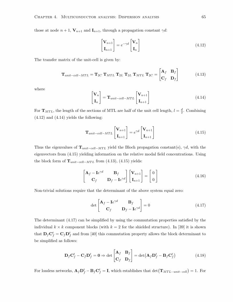
Chapter 4. Multiconductor analysis: Dispersion analysis 65
those at node n+ 1, Vn+1 and In+1, through a propagation constant γd:[Vn+1
In+1
]= e−γd
[Vn
In
](4.12)
The transfer matrix of the unit-cell is given by:
Tunit−cell−MTL = T2C TMTL T2L T2L TMTL T2C =
[Af Bf
Cf Df
](4.13)
where [Vn
In
]= Tunit−cell−MTL
[Vn+1
In+1
](4.14)
For TMTL, the length of the sections of MTL are half of the unit cell length, l = d2 . Combining
(4.12) and (4.14) yields the following:
Tunit−cell−MTL
[Vn+1
In+1
]= eγd
[Vn+1
In+1
](4.15)
Thus the eigenvalues of Tunit−cell−MTL yield the Bloch propagation constant(s), γd, with the
eigenvectors from (4.15) yielding information on the relative modal field concentrations. Using
the block form of Tunit−cell−MTL from (4.13), (4.15) yields:
[Af − Ieγd Bf
Cf Df − Ieγd
][Vn+1
In+1
]=
[0
0
](4.16)
Non-trivial solutions require that the determinant of the above system equal zero:
det
[Af − Ieγd Bf
Cf Df − Ieγd
]= 0 (4.17)
The determinant (4.17) can be simplified by using the commutation properties satisfied by the
individual k × k component blocks (with k = 2 for the shielded structure). In [39] it is shown
that DfCtf = CfDt
f and from [40] this commutation property allows the block determinant to
be simplified as follows:
DfCtf −CfDt
f = 0⇒ det
[Af Bf
Cf Df
]= det
(AfDt
f −BfCtf
)(4.18)
For lossless networks, AfDtf −BfCt
f = I, which establishes that det(TMTL−unit−cell
)= 1. For

Chapter 4. Multiconductor analysis: Dispersion analysis 66
symmetric networks, as is the case for the structure under consideration, Ctf −Cf = 0 , and
combining this with (4.18), the determinant from (4.17) simplifies to:
det
[Af − Ieγd Bf
Cf Df − Ieγd
]= det
(Af − cosh(γd)I
)= 0 (4.19)
For the shielded Sievenpiper structure this results in a quadratic equation in the variable
cosh(γd):
4 cosh2(γd) + 2 cosh(γd)f(ω) + g(ω) = 0 (4.20)
and hence describes two independent modes. The functions f(ω) and g(ω) are given by:
f(ω) =[−2 + 4 sin2
(θu2
)]+
−2 + 4
sin(θl2
)Zl −
cos(θl2
)2ω C
sin(θl2
)Zl
−cos(θl2
)2ω L
− 2 sin
(θu2
)cos(θu2
)ω C Zu
(4.21)
g(ω) =[−2 + 4 sin2
(θu2
)] ·−2 + 4
sin(θl2
)Zl −
cos(θl2
)2ω C
sin(θl2
)Zl
−cos(θl2
)2ω L
+4 sin
(θu2
)cos(θu2
) (1− 2 sin2
(θl2
))ω C Zu
+4Zl sin
(θu2
)cos(θu2
)sin(θl2
)cos(θl2
)ω2C LZu
(4.22)
The dispersion equation, (4.20) describes propagation for the periodic MTL unit cell of Fig-
ure 4.1. Before examining its full implications, an approximation to (4.20) will be examined in
the next section. The simplified, approximate analysis of Section 4.3 will yield much insight
into the dispersion of the structure. However it will not be sufficient to explain all of its proper-
ties. To that end, in Section 4.4 dispersion curves obtained from (4.20) without any additional
approximations will be revisited, which will supplement and enhance the results obtained from
the approximate model.
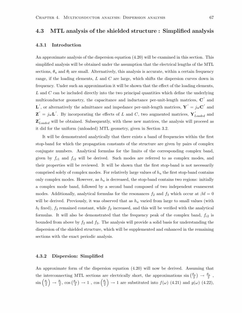
Chapter 4. Multiconductor analysis: Dispersion analysis 67
4.3 MTL analysis of the shielded structure : Simplified analysis
4.3.1 Introduction
An approximate analysis of the dispersion equation (4.20) will be examined in this section. This
simplified analysis will be obtained under the assumption that the electrical lengths of the MTL
sections, θu and θl are small. Alternatively, this analysis is accurate, within a certain frequency
range, if the loading elements, L and C are large, which shifts the dispersion curves down in
frequency. Under such an approximation it will be shown that the effect of the loading elements,
L and C can be included directly into the two principal quantities which define the underlying
multiconductor geometry, the capacitance and inductance per-unit-length matrices, C′
and
L′, or alternatively the admittance and impedance per-unit-length matrices, Y
′= jωC
′and
Z′
= jωL′. By incorporating the effects of L and C, two augmented matrices, Y
′Loaded and
Z′Loaded will be obtained. Subsequently, with these new matrices, the analysis will proceed as
it did for the uniform (unloaded) MTL geometry, given in Section 3.2.
It will be demonstrated analytically that there exists a band of frequencies within the first
stop-band for which the propagation constants of the structure are given by pairs of complex
conjugate numbers. Analytical formulas for the limits of the corresponding complex band,
given by fc1 and fc2 will be derived. Such modes are referred to as complex modes, and
their properties will be reviewed. It will be shown that the first stop-band is not necessarily
comprised solely of complex modes. For relatively large values of hu the first stop-band contains
only complex modes. However, as hu is decreased, the stop-band contains two regions: initially
a complex mode band, followed by a second band composed of two independent evanescent
modes. Additionally, analytical formulas for the resonances f2 and f3 which occur at βd = 0
will be derived. Previously, it was observed that as hu varied from large to small values (with
hl fixed), f3 remained constant, while f2 increased, and this will be verified with the analytical
formulas. It will also be demonstrated that the frequency peak of the complex band, fc2 is
bounded from above by f2 and f3. The analysis will provide a solid basis for understanding the
dispersion of the shielded structure, which will be supplemented and enhanced in the remaining
sections with the exact periodic analysis.
4.3.2 Dispersion: Simplified
An approximate form of the dispersion equation (4.20) will now be derived. Assuming that
the interconnecting MTL sections are electrically short, the approximations sin(θu2
) → θu2 ,
sin(θl2
)→ θl
2 , cos(θu2
) → 1 , cos(θl2
)→ 1 are substituted into f(ω) (4.21) and g(ω) (4.22),
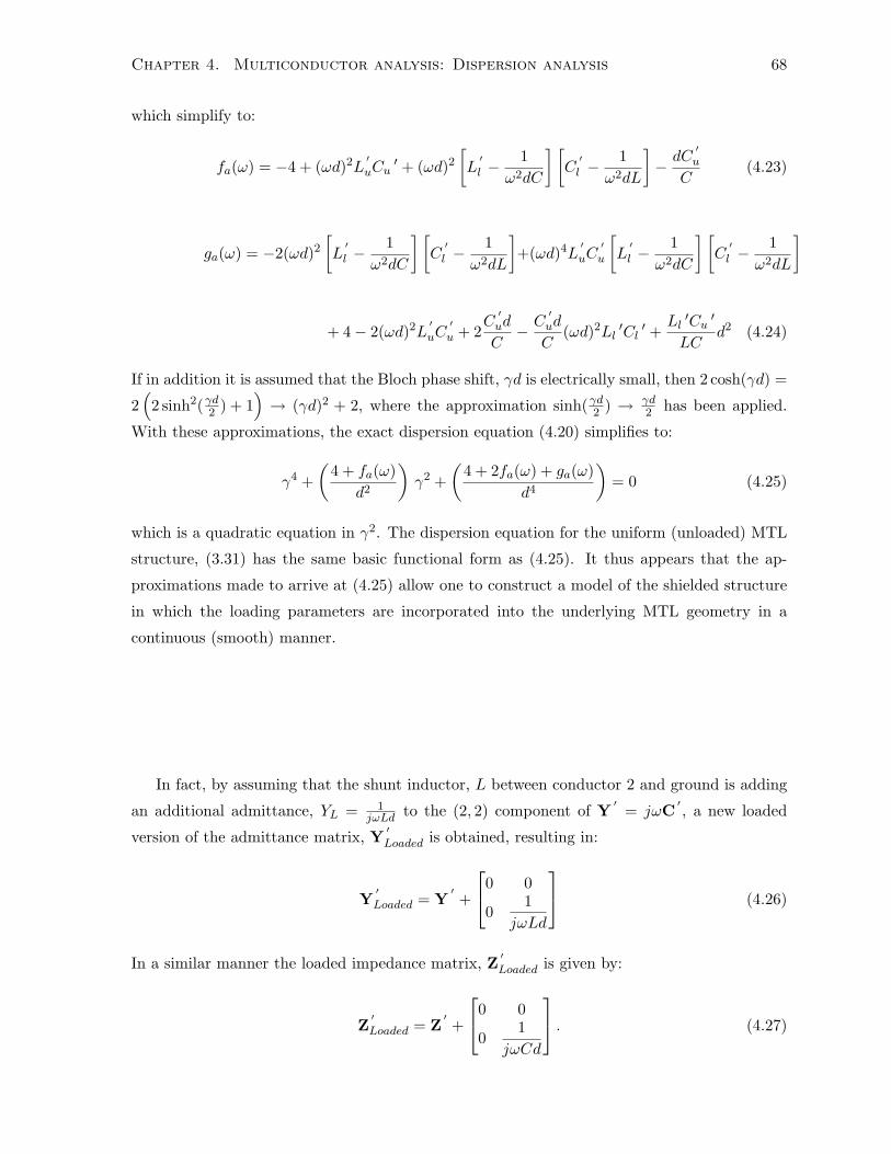
Chapter 4. Multiconductor analysis: Dispersion analysis 68
which simplify to:
fa(ω) = −4 + (ωd)2L′uCu
′ + (ωd)2[L′l −
1ω2dC
] [C′l −
1ω2dL
]− dC
′u
C(4.23)
ga(ω) = −2(ωd)2[L′l −
1ω2dC
] [C′l −
1ω2dL
]+(ωd)4L
′uC
′u
[L′l −
1ω2dC
] [C′l −
1ω2dL
]
+ 4− 2(ωd)2L′uC
′u + 2
C′ud
C− C
′ud
C(ωd)2Ll ′Cl ′ +
Ll′Cu
′
LCd2 (4.24)
If in addition it is assumed that the Bloch phase shift, γd is electrically small, then 2 cosh(γd) =
2(
2 sinh2(γd2 ) + 1)→ (γd)2 + 2, where the approximation sinh(γd2 ) → γd
2 has been applied.
With these approximations, the exact dispersion equation (4.20) simplifies to:
γ4 +(
4 + fa(ω)d2
)γ2 +
(4 + 2fa(ω) + ga(ω)
d4
)= 0 (4.25)
which is a quadratic equation in γ2. The dispersion equation for the uniform (unloaded) MTL
structure, (3.31) has the same basic functional form as (4.25). It thus appears that the ap-
proximations made to arrive at (4.25) allow one to construct a model of the shielded structure
in which the loading parameters are incorporated into the underlying MTL geometry in a
continuous (smooth) manner.
In fact, by assuming that the shunt inductor, L between conductor 2 and ground is adding
an additional admittance, YL = 1jωLd to the (2, 2) component of Y
′= jωC
′, a new loaded
version of the admittance matrix, Y′Loaded is obtained, resulting in:
Y′Loaded = Y
′+
0 0
01
jωLd
(4.26)
In a similar manner the loaded impedance matrix, Z′Loaded is given by:
Z′Loaded = Z
′+
0 0
01
jωCd
. (4.27)

Chapter 4. Multiconductor analysis: Dispersion analysis 69
with the explicit forms of Y′Loaded and Z
′Loaded given by:
Y′Loaded = jω
C′u −C ′u
−C ′u(C′u + C
′l −
1ω2Ld
) =
[Y L
1 Y Lm
Y Lm Y L
2
](4.28)
and
Z′Loaded = jω
L ′u + L′l L
′l
L′l
(L′l −
1ω2Cd
) =
[ZL1 ZLm
ZLm ZL2
](4.29)
Using the loaded matrices, (4.28) and (4.29) the analysis proceeds as it did for the uniform
MTL geometry, with the dispersion equation given by:
γ4 + (−aL1 − aL2 ) γ2 + (aL1 aL2 − bL1 bL2 ) = 0 (4.30)
The two solutions of (4.30) are:
γ2a,b =
12
[(aL1 + aL2
)±√DiscL] (4.31)
where
DiscL =(aL1 + aL2
)2 − 4(aL1 a
L2 − bL1 bL2
)(4.32)
is the discriminant of the quadratic in γ2, (4.30). The discriminant, DiscL will be shown to be
important in the appearance of complex modes. The parameters, aL1 , bL1 , aL2 , and bL2 are given
by
aL1 = −ω2CuLu (4.33)
bL1 = −ω2
[−LuCu +
(Cl − 1
ω2Ld
)Ll
](4.34)
aL2 = −ω2
[− Cuω2Cd
+(Cl − 1
ω2Ld
)(Ll − 1
ω2Cd
)](4.35)
bL2 = −ω2
[Cuω2Cd
](4.36)
Using (4.33) through (4.36) it can be shown that
− aL1 − aL2 =4 + fa(ω)
d2(4.37)
and
aL1 aL2 − bL1 bL2 =
(4 + 2fa(ω) + ga(ω)
d4
). (4.38)
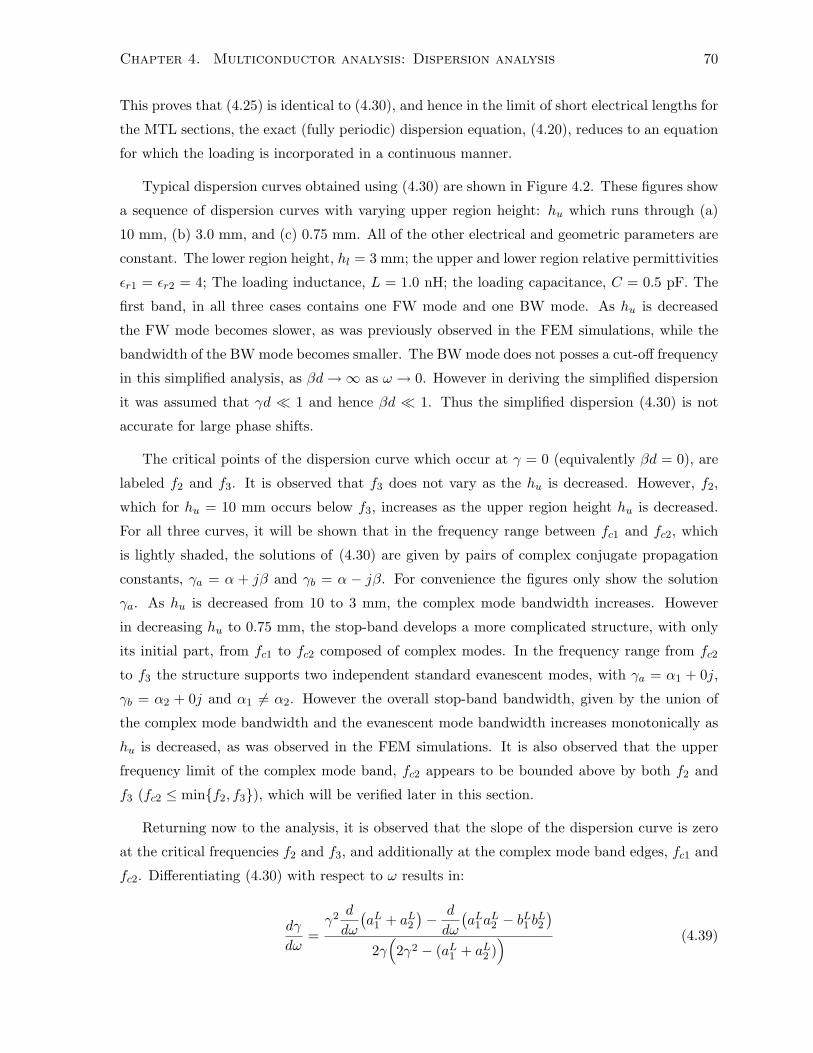
Chapter 4. Multiconductor analysis: Dispersion analysis 70
This proves that (4.25) is identical to (4.30), and hence in the limit of short electrical lengths for
the MTL sections, the exact (fully periodic) dispersion equation, (4.20), reduces to an equation
for which the loading is incorporated in a continuous manner.
Typical dispersion curves obtained using (4.30) are shown in Figure 4.2. These figures show
a sequence of dispersion curves with varying upper region height: hu which runs through (a)
10 mm, (b) 3.0 mm, and (c) 0.75 mm. All of the other electrical and geometric parameters are
constant. The lower region height, hl = 3 mm; the upper and lower region relative permittivities
εr1 = εr2 = 4; The loading inductance, L = 1.0 nH; the loading capacitance, C = 0.5 pF. The
first band, in all three cases contains one FW mode and one BW mode. As hu is decreased
the FW mode becomes slower, as was previously observed in the FEM simulations, while the
bandwidth of the BW mode becomes smaller. The BW mode does not posses a cut-off frequency
in this simplified analysis, as βd→∞ as ω → 0. However in deriving the simplified dispersion
it was assumed that γd 1 and hence βd 1. Thus the simplified dispersion (4.30) is not
accurate for large phase shifts.
The critical points of the dispersion curve which occur at γ = 0 (equivalently βd = 0), are
labeled f2 and f3. It is observed that f3 does not vary as the hu is decreased. However, f2,
which for hu = 10 mm occurs below f3, increases as the upper region height hu is decreased.
For all three curves, it will be shown that in the frequency range between fc1 and fc2, which
is lightly shaded, the solutions of (4.30) are given by pairs of complex conjugate propagation
constants, γa = α + jβ and γb = α − jβ. For convenience the figures only show the solution
γa. As hu is decreased from 10 to 3 mm, the complex mode bandwidth increases. However
in decreasing hu to 0.75 mm, the stop-band develops a more complicated structure, with only
its initial part, from fc1 to fc2 composed of complex modes. In the frequency range from fc2
to f3 the structure supports two independent standard evanescent modes, with γa = α1 + 0j,
γb = α2 + 0j and α1 6= α2. However the overall stop-band bandwidth, given by the union of
the complex mode bandwidth and the evanescent mode bandwidth increases monotonically as
hu is decreased, as was observed in the FEM simulations. It is also observed that the upper
frequency limit of the complex mode band, fc2 appears to be bounded above by both f2 and
f3 (fc2 ≤ minf2, f3), which will be verified later in this section.
Returning now to the analysis, it is observed that the slope of the dispersion curve is zero
at the critical frequencies f2 and f3, and additionally at the complex mode band edges, fc1 and
fc2. Differentiating (4.30) with respect to ω results in:
dγ
dω=γ2 d
dω
(aL1 + aL2
)− d
dω
(aL1 a
L2 − bL1 bL2
)2γ(
2γ2 − (aL1 + aL2 )) (4.39)
Chapter 4. Multiconductor analysis: Dispersion analysis 71
(a) hu = 10 mm
(b) hu = 3 mm
(c) hu = 0.75 mm
Figure 4.2: Dispersion curves obtained using the simplified dispersion equation (4.30), withvarying upper region height. (a) hu = 10 mm; (b) hu = 3 mm; (c) hu = 0.75mm. All other parameters are fixed: the lower region height, hl = 3 mm; the upperand lower region relative permittivities are εr1 = εr2 = 4; the loading inductance,L = 1.0 nH; the loading capacitance, C = 0.5 pF.

Chapter 4. Multiconductor analysis: Dispersion analysis 72
from which it is observed that dωdγ = 0 when the denominator of (4.39) is set equal to zero. The
critical points are thus given by:
γ = 0 ⇒ f2, f3 (4.40)
and
γ2 =12
(aL1 + aL2 ) ⇒ fc1, fc2 (4.41)
Substituting γ = 0 (4.40) into the dispersion equation (4.30) results in the following expression:
aL1 aL2 − bL1 bL2 = ω4C
′l L′lC′uL′u
(1− 1
ω2L(C ′l d)
)[1− 1
ω2C
(1L′l d
+1L′l d
)]. (4.42)
The zeroes of (4.42) correspond to the critical frequencies f2 and f3:
ω22 =
1C
(1L′l d
+1L ′ud
)(4.43)
and
ω23 =
1L(C ′l d)
. (4.44)
The frequency f2(ω2) corresponds to a resonance between the loading capacitance, C and a
parallel combination of two inductances, Leff1 = L′l d and Leff2 = L
′ud. The inductances Leff1
and Leff2 are due to the distributed MTL per-unit-length inductive parameters of the upper
and lower regions, L′u, and L
′l . From this expression it is seen that f2 depends on the MTL
parameters of both the upper and lower regions, and hence f2 varies as hu is varied. For a fixed
lower region height, hl, as hu is decreased, L′u = µohu
d decreases, corresponding to an increase in
f2 as is observed in Figure 4.2. On the other hand, the frequency f3 is a resonance between the
loading inductance, L and Ceff = C′l d, which is due to the lower region distributed capacitance.
Thus f3 is invariant as the upper region height is altered, as C′l = ε2w
hlis a function of the lower
region height, hl, solely.
The frequencies fc1 and fc2 are obtained when (4.41), γ2 = 12(aL1 + aL2 ) is satisfied. Substi-
tuting (4.41) into the dispersion equation (4.30) results in:
− 14
(aL1 + aL2
)2+ (aL1 a
L2 − bL1 bL2 ) = 0 (4.45)
which is zero when DiscL = 0 (4.32). The discriminant DiscL is given by:
DiscL =1ω4
(A1ω
8 +B1ω6 + C1ω
4 +D1ω2 + E1
)(4.46)

Chapter 4. Multiconductor analysis: Dispersion analysis 73
with coefficients:
A1 =(C′uL′u − C
′l L′l
)2(4.47)
B1 =(C′uL′u − C
′l L′l
)[2L′l
Ld− 2
(C′u − C
′l
)Cd
](4.48)
C1 =(C′u)2(
Cd)2 +
2C′uC
′l(
Cd)2 +
(C′l )2(
Cd)2 − 2C
′uL′u(
Cd)(Ld) − 2C
′uL′l(
Cd)(Ld) +
4C′l L′l(
Cd)(Ld) +
(L′l )
2(Ld)2 (4.49)
D1 = − 2(Cd)(Ld) (C ′u
Cd+C′l
Cd+L′l
Ld
)(4.50)
E1 =1(
Ld)2(
Cd)2 (4.51)
In general, the zeroes of (4.46) will reduce to the solution of a quartic equation in ω2. Although
closed form solutions for quartic equations exist, the formulas are quite lengthy, especially for
a situation like the case considered here where the coefficients are not numbers, but variables
themselves. However, when the condition ε1 = ε2 is satisfied it can be shown that C′uL′u = C
′l L′l ,
so that from (4.47) and (4.48) A1 = B1 = 0 and thus the zeroes of (4.46) are reduced to the
solutions of a quadratic in ω2. The two solutions are given by:
ω2c1 =
1
LC′l d+
(√LC ′ud+
√CL
′l d)2 (4.52)
and
ω2c2 =
1
LC′l d+
(√LC ′ud−
√CL
′l d)2 (4.53)
From (4.53) it is observed that:
ω2c2 ≤ ω2
3 =1
LC′l d
(4.54)
thus proving that the peak of the complex mode band at fc2 is bounded above by f3. After
some algebra (4.53) can be rewritten into another form:
ω2c2 =
1
CL′uL′l d
L ′u + L′l
+
(√LC
′l L′ud+
√LC ′uL
′l d−
√C(L ′l )
2d)2
L ′u + L′l
(4.55)
which shows that
ω2c2 ≤ ω2
2 =1C
(1L′l d
+1L ′ud
)(4.56)
Thus fc2 is bounded from above by both f2 and f3 (fc2 ≤ minf2, f3).

Chapter 4. Multiconductor analysis: Dispersion analysis 74
f2
↑f3
↑↑fc1
↑fc2
Dis
cL
0
Figure 4.3: Plot of the function DiscL, which is negative between fc1 and fc2 and otherwisepositive.
The behaviour of DiscL will now be examined. From (4.52) and (4.53) it is clear that
ω2c2 > ω2
c1 represents the larger of two real positive frequencies representing the solutions of
DiscL = 0. The asymptotic behaviour of DiscL as ω → 0 is determined by E1ω4 , and as E1 is
positive, Disc→∞ as ω → 0. The asymptotic behaviour of DiscL as ω →∞ is determined by
C1 which can also be shown to be positive, and hence Disc→ C1 as ω →∞. Thus DiscL ≤ 0
for ωc1 ≤ ω ≤ ωc2, and Disc ≥ 0 otherwise, as is shown in Figure 4.3. For the finite frequency
range when DiscL < 0, the roots of the dispersion equation are given by:
γ2a,b = p(ω)± jq(ω) (4.57)
where p(ω) = 12
(aL1 + aL2
)and q(ω) = 1
2
√|DiscL| are purely real numbers. The solutions of
(4.57) are given by:
γa = ±(α(ω) + jβ(ω))
γb = ±(α(ω)− jβ(ω)). (4.58)
One pair of complex modes corresponds to exponential decay, γa,b(1) = α(ω)± jβ(ω) while
the other pair corresponds to exponential increase, γa,b(2) = −α(ω) ± jβ(ω). Both the real,
α(ω) and imaginary parts, β(ω) of γa,b have frequency variation within the complex mode band.
Each complex mode has a real power flow, which is oppositely directed in the upper and lower
regions, in such a manner that the net integrated power over a transverse cross-section is zero
[38]. In addition, there is no net reactive energy associated with a single complex mode, unlike
the case for standard evanescent modes.
In Figure 4.4 the stop-band is depicted for the two cases: (a) relatively large hu and (b)

Chapter 4. Multiconductor analysis: Dispersion analysis 75
f2 →
f3 →
ւ fc1
← fc2
βdαd
γa = jβaγb = jβb
γa = jβ + αγb = −jβ + α
jβa jβb
(a) Relatively large hu: stop-band consists solely of complex modes.
f3 →
ւ fc1
← fc2
βd
αd
γa = jβa γb = jβb
γa = jβ + αγb = −jβ + α
γa = αa γb = αb
(b) Relatively small hu: stop-band consists of both complex modes (light shading) and evanescentmodes (dark shading).
Figure 4.4: Power flow profiles for complex modes with complex-conjugate propagation con-stants, γa = jβ + α and γb = −jβ + α.

Chapter 4. Multiconductor analysis: Dispersion analysis 76
relatively small hu. It is observed that for large hu the stop-band is characterized completely by
complex modes. The real part of the power flow for the two independent modes, characterized
by complex conjugate propagation constants, is depicted in the figure. It is seen that for the two
modes characterized by exponential decay, the real power flow in the upper and lower regions
are reversed. This would seem to suggest that the possibility of exciting a single complex mode
would depend on the region in which the structure is excited, either upper or lower. In fact
it will be shown in Chapter 6 that it possible to strongly excite a single complex mode with
a properly confined excitation. However, if the structure is excited with a source which is not
confined to a single region it will be shown that both exponentially decaying complex modes are
strongly excited. For the small hu case, Figure 4.4b shows that only the initial part of the stop-
band is composed of complex modes. Above the complex mode band, there exists a stop-band
in which two independent evanescent modes, with γa = αa and γb = αb are supported. It will
be shown in Chapter 6 that the signature of the complex stop-band has a different character
than that of a stop-band formed from standard evanescent modes, when a finite cascade of unit
cells of the structure is excited.
4.4 MTL analysis of the shielded structure (b): Comparison of
full periodic dispersion with FEM simulations
Having derived the dispersion equation for the periodic unit cell in Section 4.2, and then exam-
ining it using a simplifying approximation in Section 4.3, the dispersion curves generated using
the fully periodic MTL dispersion equation (4.20) will now be compared with FEM simulated
results. The simulation software could not readily calculate the propagation constants within
the stop-band. However, as the MTL model is able to obtain the propagation constants within
stop-bands, they are included for convenience and will be validated in Chapter 6, where the
scattering properties of finite cascades of unit cells are considered.
The FEM generated dispersion curves correspond to a series of simulations in which the
upper region height, hu, is given six values: hu = 18, 12, 6, 1, 0.5 and 0.2 mm, and are shown in
Figure 4.5 (a) through (f). All of the other electrical and geometric parameters of the structure
are fixed. The upper and lower region permittivities are εr1 = 1 and εr2 = 2.3, respectively,
while the periodicity and patch width are d = 10 mm and w = 9.6 mm, respectively. The via
radius is r = 0.5 mm. It is recalled that the series capacitance, C, used in the MTL model is
dependent on the upper region height, and thus for each upper region height a different value
for C was used, with C varying from 0.28 pF for hu = 18 mm, to 0.16 pF for hu = 0.2 mm,
as calculated using the four port scattering set-up described in Chapter 3. The inductance
L, is independent of the upper region height and its value is calculated to be 0.75 nH, again
Chapter 4. Multiconductor analysis: Dispersion analysis 77
using the scattering analysis described in Chapter 3. The FEM generated dispersion curves are
obtained by varying the phase along x, (βd)x, while the phase shift transverse to the direction
of propagation is fixed, (βd)y = 0.
The simulations were performed on a PC using an Intel(R) Xeon(R) CPU 5160, with a
clock rate of 3.00 GHz, and with 16.0 GB of RAM. The simulation was terminated when the
difference in modal frequency between successive passes was below 0.2 %. In order to obtain
the dispersion diagram two sets of simulations were performed; first the lower band modes, and
then the remaining upper band modes. The reason for this was that the eigenmode frequency
extraction requires one to set a minimum frequency for a given simulation, and it was found that
since the upper band modes occur much higher in frequency, it was advantageous to split up
the simulation into two sets, so as to allow for faster convergence of the upper band modes. The
simulation time for a lower band mode was approximately 2 minutes for a single (βxd) value,
while the upper band modes required appoximately 5 minutes for a single (βxd) value. The
dispersion curves were obtained by sweeping over the (βxd) values in 5 increments resulting
in 37 points from 0 to 180 (π radians), for a total simulation time of approximately 4.5 hours
per geometry. Even though the FEM curves are obtained with a fixed transverse phase shift
(βd)y = 0, it was shown in Chapter 2 that the modes thus obtained could be divided into
two classes with different field polarizations at the transverse boundaries. The FEM simulated
dispersion curves defining these two classes have been marked with squares, (FEM), and
circles, (FEM-TE).
For large values of hu, corresponding to hu = 18, 12, and 6 mm, the general form of the
dispersion curves are similar to those obtained using the simplified analysis, with the exception
of a cut-off frequency, f1, at βd = π for the lowest backward wave mode, due to the structure’s
periodicity. This is in contrast to the simplified analysis were there was no limit on βd, which
asymptotically approached infinity as frequency approached zero. Additionally, another reso-
nance for βd = π occurs at f4, which is again due to the periodicity. It is observed that the
MTL generated curves match extremely well within the pass-band of the structure with the
FEM curves, with the exception of the FEM (TE) mode. The FEM(TE) mode is not captured
by the MTL model, as it is not a quasi-TEM mode as was seen in Chapter 2. There is a modal
degeneracy at f2, with one mode emerging from f2 captured by the MTL model, and the other
mode being the TE mode. This degeneracy will be explained in Section 4.8. As in the simplified
approximation, for large values of hu, the stop-band is composed entirely of complex modes,
with the complex mode band situated between the frequencies, fc1 and fc2. As hu is decreased
from 18 to 6 mm, the complex mode bandwidth increases, as does the value of α within the
complex mode band, indicating a stronger interaction between the upper and lower regions as
hu is decreased. The resonance frequencies f3 and f4 are invariant as well.
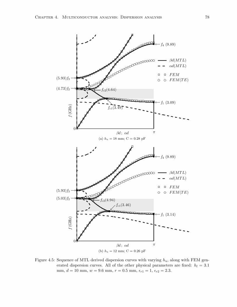
Chapter 4. Multiconductor analysis: Dispersion analysis 78
(a) hu = 18 mm; C = 0.28 pF
(b) hu = 12 mm; C = 0.26 pF
Figure 4.5: Sequence of MTL derived dispersion curves with varying hu, along with FEM gen-erated dispersion curves. All of the other physical parameters are fixed: hl = 3.1mm, d = 10 mm, w = 9.6 mm, r = 0.5 mm, εr1 = 1, εr2 = 2.3.
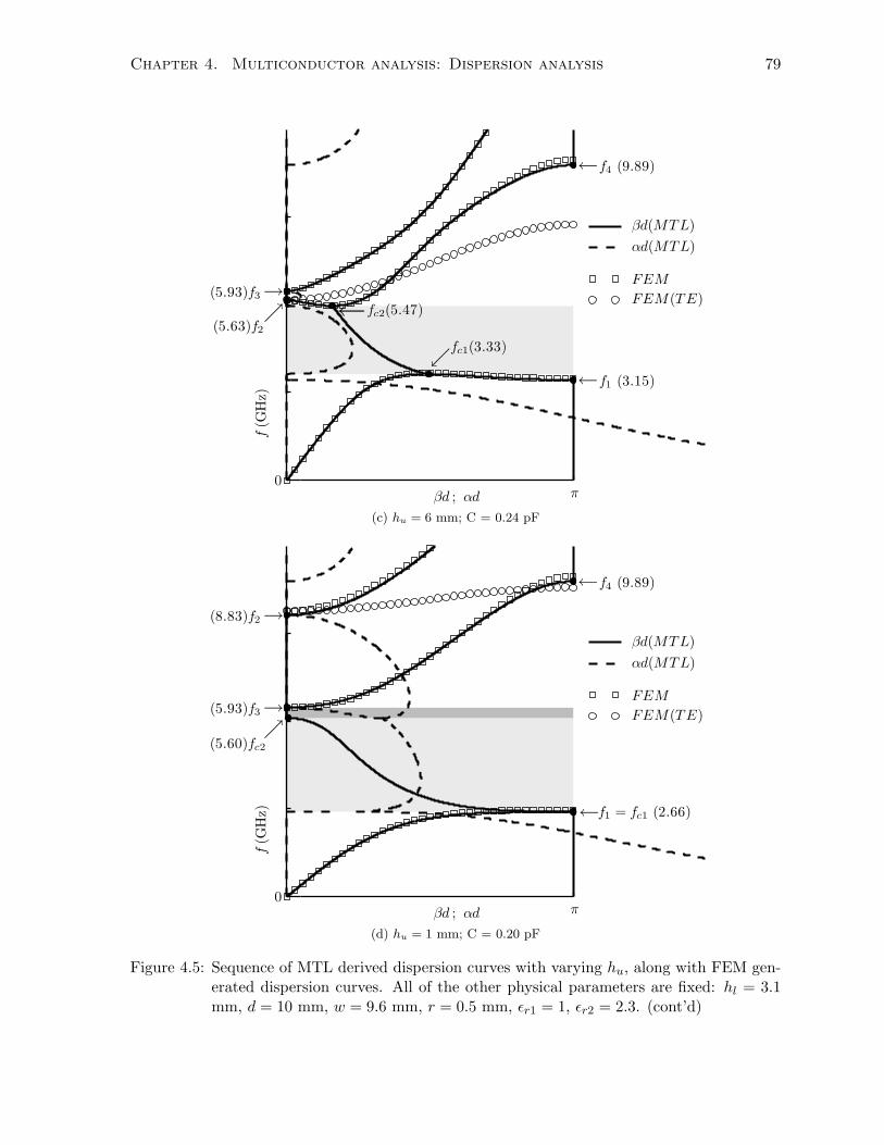
Chapter 4. Multiconductor analysis: Dispersion analysis 79
(c) hu = 6 mm; C = 0.24 pF
(d) hu = 1 mm; C = 0.20 pF
Figure 4.5: Sequence of MTL derived dispersion curves with varying hu, along with FEM gen-erated dispersion curves. All of the other physical parameters are fixed: hl = 3.1mm, d = 10 mm, w = 9.6 mm, r = 0.5 mm, εr1 = 1, εr2 = 2.3. (cont’d)
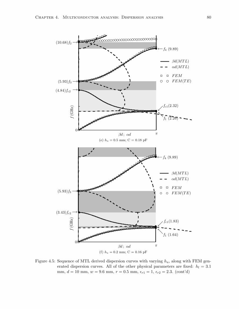
Chapter 4. Multiconductor analysis: Dispersion analysis 80
(e) hu = 0.5 mm; C = 0.18 pF
(f) hu = 0.2 mm; C = 0.16 pF
Figure 4.5: Sequence of MTL derived dispersion curves with varying hu, along with FEM gen-erated dispersion curves. All of the other physical parameters are fixed: hl = 3.1mm, d = 10 mm, w = 9.6 mm, r = 0.5 mm, εr1 = 1, εr2 = 2.3. (cont’d)
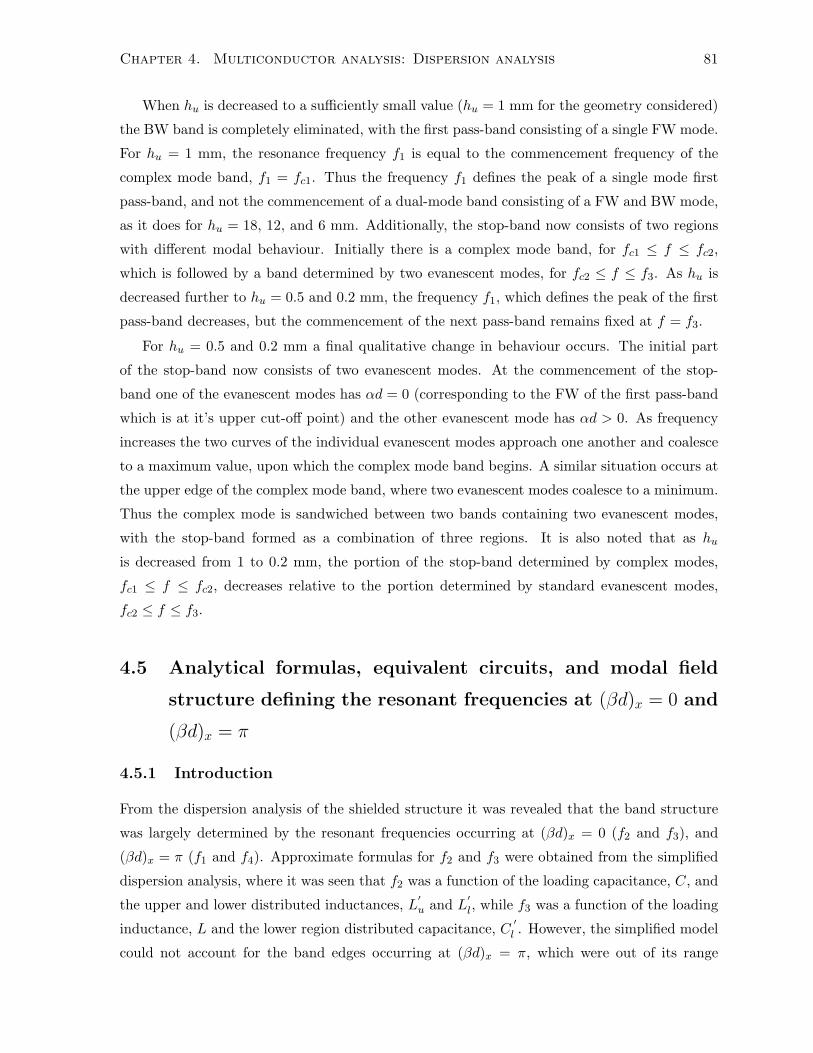
Chapter 4. Multiconductor analysis: Dispersion analysis 81
When hu is decreased to a sufficiently small value (hu = 1 mm for the geometry considered)
the BW band is completely eliminated, with the first pass-band consisting of a single FW mode.
For hu = 1 mm, the resonance frequency f1 is equal to the commencement frequency of the
complex mode band, f1 = fc1. Thus the frequency f1 defines the peak of a single mode first
pass-band, and not the commencement of a dual-mode band consisting of a FW and BW mode,
as it does for hu = 18, 12, and 6 mm. Additionally, the stop-band now consists of two regions
with different modal behaviour. Initially there is a complex mode band, for fc1 ≤ f ≤ fc2,
which is followed by a band determined by two evanescent modes, for fc2 ≤ f ≤ f3. As hu is
decreased further to hu = 0.5 and 0.2 mm, the frequency f1, which defines the peak of the first
pass-band decreases, but the commencement of the next pass-band remains fixed at f = f3.
For hu = 0.5 and 0.2 mm a final qualitative change in behaviour occurs. The initial part
of the stop-band now consists of two evanescent modes. At the commencement of the stop-
band one of the evanescent modes has αd = 0 (corresponding to the FW of the first pass-band
which is at it’s upper cut-off point) and the other evanescent mode has αd > 0. As frequency
increases the two curves of the individual evanescent modes approach one another and coalesce
to a maximum value, upon which the complex mode band begins. A similar situation occurs at
the upper edge of the complex mode band, where two evanescent modes coalesce to a minimum.
Thus the complex mode is sandwiched between two bands containing two evanescent modes,
with the stop-band formed as a combination of three regions. It is also noted that as huis decreased from 1 to 0.2 mm, the portion of the stop-band determined by complex modes,
fc1 ≤ f ≤ fc2, decreases relative to the portion determined by standard evanescent modes,
fc2 ≤ f ≤ f3.
4.5 Analytical formulas, equivalent circuits, and modal field
structure defining the resonant frequencies at (βd)x = 0 and
(βd)x = π
4.5.1 Introduction
From the dispersion analysis of the shielded structure it was revealed that the band structure
was largely determined by the resonant frequencies occurring at (βd)x = 0 (f2 and f3), and
(βd)x = π (f1 and f4). Approximate formulas for f2 and f3 were obtained from the simplified
dispersion analysis, where it was seen that f2 was a function of the loading capacitance, C, and
the upper and lower distributed inductances, L′u and L
′l, while f3 was a function of the loading
inductance, L and the lower region distributed capacitance, C′l . However, the simplified model
could not account for the band edges occurring at (βd)x = π, which were out of its range
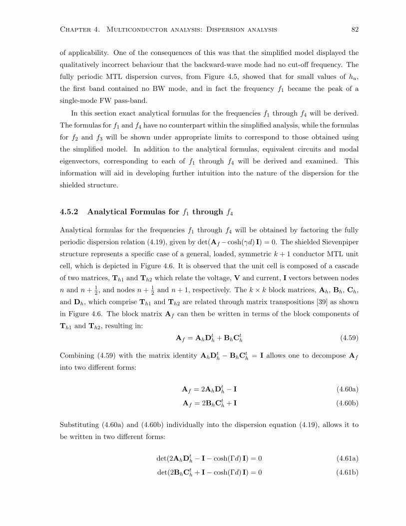
Chapter 4. Multiconductor analysis: Dispersion analysis 82
of applicability. One of the consequences of this was that the simplified model displayed the
qualitatively incorrect behaviour that the backward-wave mode had no cut-off frequency. The
fully periodic MTL dispersion curves, from Figure 4.5, showed that for small values of hu,
the first band contained no BW mode, and in fact the frequency f1 became the peak of a
single-mode FW pass-band.
In this section exact analytical formulas for the frequencies f1 through f4 will be derived.
The formulas for f1 and f4 have no counterpart within the simplified analysis, while the formulas
for f2 and f3 will be shown under appropriate limits to correspond to those obtained using
the simplified model. In addition to the analytical formulas, equivalent circuits and modal
eigenvectors, corresponding to each of f1 through f4 will be derived and examined. This
information will aid in developing further intuition into the nature of the dispersion for the
shielded structure.
4.5.2 Analytical Formulas for f1 through f4
Analytical formulas for the frequencies f1 through f4 will be obtained by factoring the fully
periodic dispersion relation (4.19), given by det(Af−cosh(γd) I) = 0. The shielded Sievenpiper
structure represents a specific case of a general, loaded, symmetric k + 1 conductor MTL unit
cell, which is depicted in Figure 4.6. It is observed that the unit cell is composed of a cascade
of two matrices, Th1 and Th2 which relate the voltage, V and current, I vectors between nodes
n and n+ 12 , and nodes n+ 1
2 and n+ 1, respectively. The k × k block matrices, Ah, Bh, Ch,
and Dh, which comprise Th1 and Th2 are related through matrix transpositions [39] as shown
in Figure 4.6. The block matrix Af can then be written in terms of the block components of
Th1 and Th2, resulting in:
Af = AhDth + BhCt
h (4.59)
Combining (4.59) with the matrix identity AhDth − BhCt
h = I allows one to decompose Af
into two different forms:
Af = 2AhDth − I (4.60a)
Af = 2BhCth + I (4.60b)
Substituting (4.60a) and (4.60b) individually into the dispersion equation (4.19), allows it to
be written in two different forms:
det(2AhDth − I− cosh(Γd) I) = 0 (4.61a)
det(2BhCth + I− cosh(Γd) I) = 0 (4.61b)
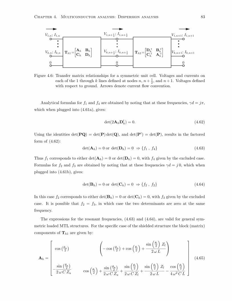
Chapter 4. Multiconductor analysis: Dispersion analysis 83
Th1 =[Ah Bh
Ch Dh
]Th2 =
[D t
h B th
C th A t
h
]V1,n; I1,n
Vk,n; Ik,n
000
V1,n+ 12; I1,n+ 1
2
Vk,n+ 12; Ik,n+ 1
2
V1,n+1; I1,n+1
Vk,n+1; Ik,n+1
Figure 4.6: Transfer matrix relationships for a symmetric unit cell. Voltages and currents oneach of the 1 through k lines defined at nodes n, n+ 1
2 , and n+ 1. Voltages definedwith respect to ground. Arrows denote current flow convention.
Analytical formulas for f1 and f4 are obtained by noting that at these frequencies, γd = jπ,
which when plugged into (4.61a), gives:
det(2AhDth) = 0. (4.62)
Using the identities det(PQ) = det(P) det(Q), and det(Pt) = det(P), results in the factored
form of (4.62):
det(Ah) = 0 or det(Dh) = 0 ⇒ f1 , f4 (4.63)
Thus f1 corresponds to either det(Ah) = 0 or det(Dh) = 0, with f4 given by the excluded case.
Formulas for f2 and f3 are obtained by noting that at these frequencies γd = j 0, which when
plugged into (4.61b), gives:
det(Bh) = 0 or det(Ch) = 0 ⇒ f2 , f2 (4.64)
In this case f2 corresponds to either det(Bh) = 0 or det(Ch) = 0, with f3 given by the excluded
case. It is possible that f2 = f3, in which case the two determinants are zero at the same
frequency.
The expressions for the resonant frequencies, (4.63) and (4.64), are valid for general sym-
metric loaded MTL structures. For the specific case of the shielded structure the block (matrix)
components of Th1 are given by:
Ah =
cos(θu2
) − cos(θu2
)+ cos
(θl2
)+
sin(θl2
)Zl
2ω L
− sin(θu2
)2ω C Zu cos
(θl2
)+
sin(θu2
)2ω C Zu
+sin(θl2
)2ω C Zl
+sin(θl2
)Zl
2ω L−
cos(θl2
)4ω2C L
(4.65)
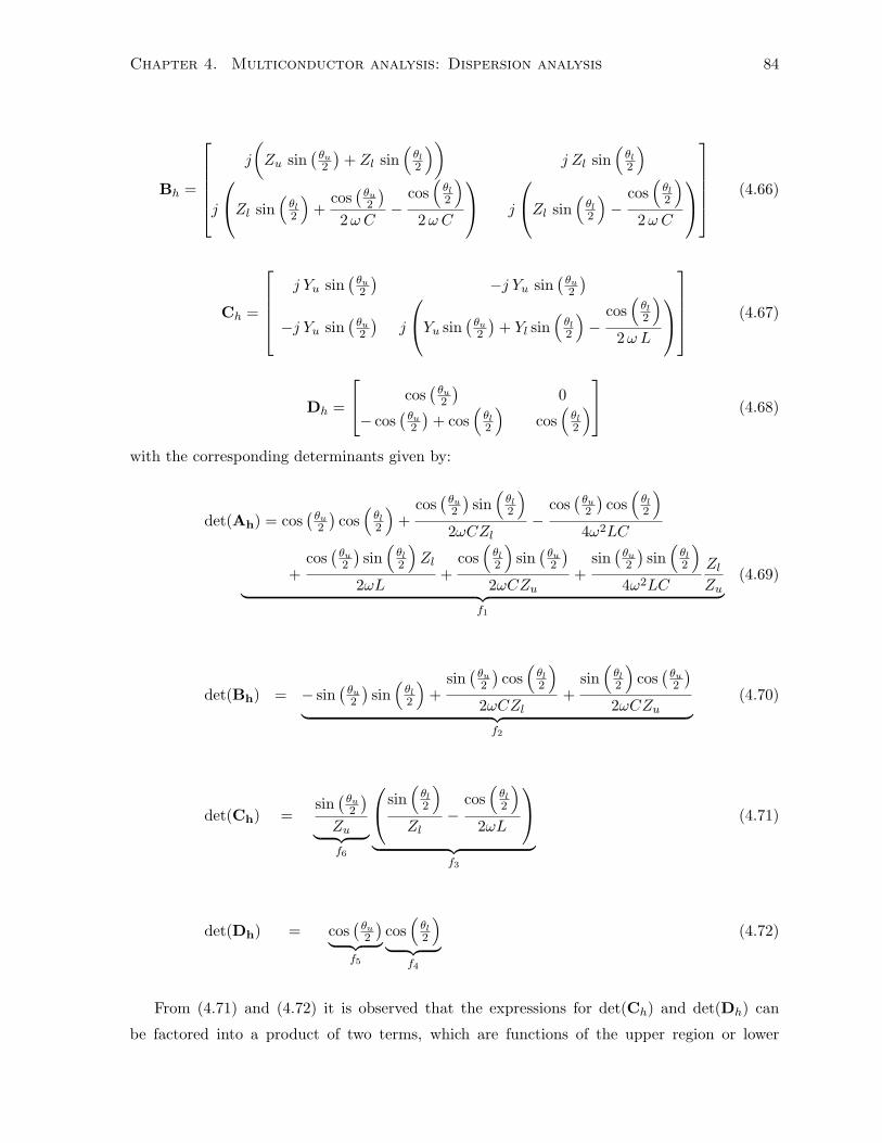
Chapter 4. Multiconductor analysis: Dispersion analysis 84
Bh =
j
(Zu sin
(θu2
)+ Zl sin
(θl2
))j Zl sin
(θl2
)j
Zl sin(θl2
)+
cos(θu2
)2ω C
−cos(θl2
)2ω C
j
Zl sin(θl2
)−
cos(θl2
)2ω C
(4.66)
Ch =
j Yu sin
(θu2
) −j Yu sin(θu2
)−j Yu sin
(θu2
)j
Yu sin(θu2
)+ Yl sin
(θl2
)−
cos(θl2
)2ω L
(4.67)
Dh =
cos(θu2
)0
− cos(θu2
)+ cos
(θl2
)cos(θl2
) (4.68)
with the corresponding determinants given by:
det(Ah) = cos(θu2
)cos(θl2
)+
cos(θu2
)sin(θl2
)2ωCZl
−cos(θu2
)cos(θl2
)4ω2LC
+cos(θu2
)sin(θl2
)Zl
2ωL+
cos(θl2
)sin(θu2
)2ωCZu
+sin(θu2
)sin(θl2
)4ω2LC
ZlZu︸ ︷︷ ︸
f1
(4.69)
det(Bh) = − sin(θu2
)sin(θl2
)+
sin(θu2
)cos(θl2
)2ωCZl
+sin(θl2
)cos(θu2
)2ωCZu︸ ︷︷ ︸
f2
(4.70)
det(Ch) =sin(θu2
)Zu︸ ︷︷ ︸f6
sin(θl2
)Zl
−cos(θl2
)2ωL
︸ ︷︷ ︸
f3
(4.71)
det(Dh) = cos(θu2
)︸ ︷︷ ︸f5
cos(θl2
)︸ ︷︷ ︸
f4
(4.72)
From (4.71) and (4.72) it is observed that the expressions for det(Ch) and det(Dh) can
be factored into a product of two terms, which are functions of the upper region or lower

Chapter 4. Multiconductor analysis: Dispersion analysis 85
region parameters alone. The factors corresponding to f3 and f4 involve only terms containing
the lower region MTL geometry, which verifies the previous observation that both f3 and f4
remained constant as long as the lower region height, hl was constant. For the sequence of
dispersion curves shown in Figure 4.5 only hu was varied with hl remaining fixed, and indeed it
is observed that both f3 and f4 are invariant. The remaining factors of these two determinants
yield two additional resonances, f5 and f6 which occurred at higher frequencies than depicted
in Figure 4.5. However, both f5 and f6 involve only the upper region geometry.
Conversely, the expressions for det(Ah) and det(Bh) cannot be factored as a product of
functions involving the upper and lower regions separately, and hence when either hl or huis varied, both f1 and f2 will vary, as seen in sequence of curves shown in Figure 4.5. The
resonance f2 involves the loading series capacitor, C and the MTL geometry of both regions,
while the resonance f1 involves both loading elements L and C and the MTL parameters of
both regions.
4.5.3 Equivalent Circuits for f1 through f4
Having obtained analytical formulas for f1 through f4, equivalent circuits corresponding to
these frequencies will now be established. Although the equivalent circuits presented will be
valid for general symmetric loaded MTL structures, intuition on how to obtain these is most
easily provided by looking at the analytical formulas for the resonant frequencies of the shielded
structure.
In particular, the expression for det(Dh) = cos(θu2
)cos(θl2
)(4.72), corresponding to f4
and f5, involves neither of the loading elements, L or C. Additionally, the individual factors
of det(Dh) are zero when θu = π and θl = π, corresponding to half wavelengths of the upper
and lower region modes fitting in one unit cell, d = λu2 and d = λl
2 , respectively. It thus
appears that f4 and f5 correspond to frequencies where standing-wave patterns develop in the
upper and lower regions, respectively. Intuitively, one would expect that associated with such
standing wave patterns, the terminal boundary conditions would correspond to either open
of short circuits. However, such boundary conditions would also have to correspond to the
possible excitation (or lack thereof) of the loading elements, 2C, and 2L which are located
at the edge (n, n + 1) and central (n + 12) nodes, respectively. From the symmetric cell of
the shielded structure, depicted in Figure 4.1, it is observed that if the outer nodes, n, n + 1
are left open circuited, with In = In+1 = 0, then the loading capacitance, 2C will not have
current passing through it and hence will not be excited. From Bloch’s theorem if In = 0, then
In+1 = Ineγd = 0, and thus a homogeneous boundary condition at node n implies the same
condition at node n+ 1. In fact, the physical structure of the resonance is identical, up to sign,
in both halves of the symmetric unit cell. In a similar manner, if the central node, n + 12 is
Chapter 4. Multiconductor analysis: Dispersion analysis 86
short circuited, Vn+ 12
= 0, then the loading inductance, L, will be shorted out and hence not
excited.
From the above discussion it is expected that the boundary conditions, In = In+1 = 0,
along with Vn+ 12
= 0 correspond to det(Dh) = 0, and hence f4 (and f5). To show that this is
indeed the case, the transfer matrices relating quantities between nodes n and n+ 12 , and nodes
n+ 12 and n+ 1, shown in Figure 4.6 are required:
[Vn
In
]=
[Ah Bh
Ch Dh
]Vn+ 12
In+ 12
(4.73)
and Vn+ 12
In+ 12
=
[Dth Bt
h
Cth At
h
][Vn+1
In+1
]. (4.74)
Substituting In = 0, Vn+ 12
= 0 into (4.73) yields:
DhIn+ 12
= 0 (4.75a)
Vn = BhIn+ 12
(4.75b)
A non-trivial solution for (4.75a) (and hence (4.75b)) requires det(Dh) = 0. This establishes
the desired result for the network between nodes n and n+ 12 . For the other symmetric half of
the unit cell plugging In+1 = 0, Vn+ 12
= 0 into (4.74) yields:
DthVn+1 = 0 (4.76a)
In+ 12
= CthVn+1 (4.76b)
with a non-trivial solution for (4.76a) (and hence (4.76b)) requiring det(Dth) = det(Dh) = 0.
Thus, the homogeneous boundary conditions, In = In+1 = 0 and Vn+ 12
= 0 imply that
det(Dh) = 0, corresponding to f4 and f5. The non-zero variables at resonance are obtained by
solving the homogenous system, (4.75a), resulting in In+ 126= 0. Substituting the solution of
(4.75a) into (4.75b) gives Vn 6= 0. The variable Vn+1 may be obtained from the set of equations,
(4.76a) and (4.76b), but due to Bloch’s theorem this is not necessary as Vn+1 = Vneγd =
Vnejπ = −Vn. Thus, due to the symmetry of the unit cell the physical structure of the non-
zero variables in either half of the unit cell are identical up to sign (symmetric/antisymmetric),
and hence only the variables in one half of the unit cell need to be calculated. In summary, 3 of
the 6 vector variables at the outer (n and n+ 1) and central (n+ 12) nodes are zero, while the
other three are in general non-zero. The non-zero variables are in fact the modal eigenvectors,

Chapter 4. Multiconductor analysis: Dispersion analysis 87
f1
f2
f3
f4 OpenOpen
OpenOpenOpen
Open
Short
ShortShortShort
ShortShort
2L2L 2C2C
MTL(
d2
)MTL
(d2
)
Figure 4.7: The four resonant circuits corresponding to f1 through f4 for the shielded structure.
and will be examined in Sections 4.5.4 through 4.5.7, yielding further insight into the dispersion
curves.
In a similar manner, equivalent circuits corresponding to the four resonance frequencies, f1
through f4, of the shielded structure, may be determined, and are shown in Figure 4.7. Table 4.1
compiles the boundary conditions, analytical formulas, and homogenous systems (which yield
the modal eigenvectors) for general symmetric loaded MTL structures. It is observed that a
given set of boundary conditions implies a specific zero determinant, but that the resulting
frequency may alternate: (f1 or f4) and (f2 or f3). This is most easily seen by examining the
case worked out above for the shielded structure. Had the unit cell of the shielded structure
been chosen so that the inductors, 2L, were located at nodes n and n+ 1, with the two series
capacitors, 2C, located at n + 12 , then the terminal boundary conditions corresponding to f4
would be the dual(In = In+1 = 0 → Vn = Vn+1 = 0 and Vn+ 1
2= 0 → In+ 1
2= 0
)of those
shown in Figure 4.7.
4.5.4 Modal field structure for f4 and f5 (at (βd)x = π)
In the previous two sections analytical formulas, and equivalent circuits, corresponding to the
band-edge frequencies f1 through f4 were derived. Two additional resonances, at f5 and f6,
which occurred out of the frequency range considered in previous simulations, were also shown.
The results of Sections 4.5.2 and 4.5.3 will now be used to calculate the modal eigenvectors at
these critical frequencies, which will provide further intuition into the nature of, and parameters
affecting, the dispersion behaviour of the shielded structure. In Section 4.5.3 it was shown
that the modal eigenvectors at resonance could be determined by considering one half of the
symmetric unit cell, with homogeneous boundary conditions associated with one of the pair

Chapter 4. Multiconductor analysis: Dispersion analysis 88
Table 4.1: Boundary conditions and analytical formulas corresponding to the resonance fre-quencies at (βd)x = 0 and (βd)x = π.
Boundary Conditions Formula Non-Zero Variables phase shift / frequency
Vn = Vn+1 = 0In+ 1
2= 0 ⇒ det(Ah) = 0
AhVn+ 12
= 0In = ChVn+ 1
2
In+1 = −In
(βd)x = π (f1 or f4)
Vn = Vn+1 = 0Vn+ 1
2= 0 ⇒ det(Bh) = 0
BhIn+ 12
= 0In = DhIn+ 1
2
In+1 = In
(βd)x = 0 (f2 or f3)
In = In+1 = 0In+ 1
2= 0 ⇒ det(Ch) = 0
ChVn+ 12
= 0Vn = AhVn+ 1
2
Vn+1 = Vn
(βd)x = 0 (f3 or f2)
In = In+1 = 0Vn+ 1
2= 0 ⇒ det(Dh) = 0
DhIn+ 12
= 0Vn = BhIn+ 1
2
Vn+1 = −Vn
(βd)x = π (f4 or f1)
of vector variables at node n, Vn, In, and one of pair at node n + 12 , Vn+ 1
2, In+ 1
2. The
complimentary non-zero variables are obtained by solving the homogenous systems shown in
Table 4.1.
The frequencies f4 and f5 are characterized by the homogenous conditions In = 0, and
Vn+ 12
= 0. The corresponding nonzero variables, In+ 12, and Vn are obtained by solving the
complimentary homogenous system, DhIn+ 12
= 0, and finally Vn is obtained from Vn =
BhIn+ 12, as in the last row of Table 4.1. Since det(Dh) = cos
(θl2
)cos(θu2
)can by factored,
its zeroes occur at two different frequencies, corresponding to f4 and f5. The frequency f4
corresponds to cos(θl2
)= 0. Solving for the frequency yields:
ω4 =π
d√L′lC′l
(4.77)
When cos(θl2
)= 0 the homogeneous system DhIn+ 1
2= 0, with Dh given in (4.68) reduces to:
[cos(θu2
)0
− cos(θu2
)0
]I (1)
n+ 12
I(2)
n+ 12
=
[0
0
](4.78)
with solution:
In+ 12
=
I (1)
n+ 12
I(2)
n+ 12
=
[0
Io
], (4.79)
Chapter 4. Multiconductor analysis: Dispersion analysis 89
where Io is an arbitrary constant. The corresponding solution for Vn is given by:
Vn =
[V
(1)n
V(2)n
]=
[Vo
Vo
](4.80)
where Vo is an arbitrary constant. Thus the modal eigenvectors at nodes n and n + 12 corre-
sponding to f4 are given by:
f4 ⇒[Vn
In
]=
Vo
Vo
0
0
and
Vn+ 12
In+ 12
=
0
0
0
Io
(4.81)
The fields described by (4.81) are only non-zero in the lower region and represent a standing
wave pattern with a half wavelength, λl2 = d, fitting within a unit cell, as shown in Figure 4.8a.
As was mentioned previously, due to the symmetry of the unit cell only one half of the cell is
considered and hence the standing wave pattern depicted in Figure 4.8a shows only a quarter
wavelength, λl4 .
In a similar manner, f5 corresponds to cos(θu2
)= 0, with the solution:
ω5 =π
d√L′uC
′u
(4.82)
and corresponding modal eigenvectors given by:
f5 ⇒[Vn
In
]=
Vo
0
0
0
and
Vn+ 12
In+ 12
=
0
0
Io
−Io
(4.83)
which has non-zero fields only in the upper region of the structure and represents a standing
wave pattern with λu2 = d, as shown in Figure 4.8b. This resonance occurred above the frequency
range of the previously shown dispersion curves.
4.5.5 Modal field structure for f3 and f6 (at (βd)x = 0)
The non-zero variables, Vn and Vn+ 12
for the condition det(Ch) = 0, (4.71), also occur at
two different frequencies corresponding to upper and lower region field concentration, and are
depicted in Figure 4.9. The frequency f6 corresponds to sin(θu2
)= 0⇒ θu = 2π, with solution
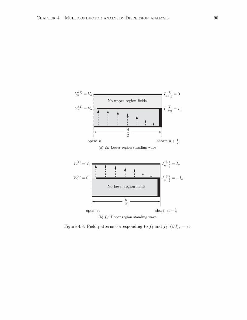
Chapter 4. Multiconductor analysis: Dispersion analysis 90
open: n short: n + 12
d
2
V(1)n = Vo
V(2)n = Vo
I(1)
n+ 12
= 0
I(2)
n+ 12
= Io
No upper region fields
(a) f4: Lower region standing wave
open: n short: n + 12
d
2
V(1)n = Vo
V(2)n = 0
I(1)
n+ 12
= Io
I(2)
n+ 12
= −Io
No lower region fields
(b) f5: Upper region standing wave
Figure 4.8: Field patterns corresponding to f4 and f5; (βd)x = π.

Chapter 4. Multiconductor analysis: Dispersion analysis 91
open: nopen: n
d
2
V(1)n = Vo
V(2)n = 0
V(1)
n+ 12
= −Vo
V(2)
n+ 12
= 0
No lower region fieldsNo lower region fields
(a) f6: Upper region standing wave
open: nopen: n
d
2
V(1)n = Vo
V(2)n = Vo
V(1)
n+ 12
= Vo
V(2)
n+ 12
= Vo
No upper region fields
(b) f3: Resonance between L and C′l d
Figure 4.9: Field patterns corresponding to f6 and f3; (βd)x = 0.
given by:
ω6 =2π
d√L′uC
′u
(4.84)
which is one full wavelength fitting within the unit cell, with field structure depicted in Fig-
ure 4.9a. This resonance was not observed in the previous dispersion plots, as it occurred out
of their range.
Setting the other factor equal to zero results in f3. The resonances considered up to this
point, f4, f5, and f6 occurred at frequencies for which the electrical lengths of the interconnect-
ing MTL sections were not negligible, and have no counterparts from the simplified analysis.
However, a simplified formula for f3 may be derived under the assumption that the MTL sec-
tions are electrically short, so that the substitutions sin(θl2
)→ θl
2 , cos(θl2
)→ 1 can be made.
With these substitutions, the equation det(Ch) = 0 may be solved for ω3 yielding:
ω23 =
1L(C ′l d)
=1
2L(C′l d
2
) (4.85)
which represents a resonance between the loading inductance, L, and the distributed lower

Chapter 4. Multiconductor analysis: Dispersion analysis 92
region capacitance multiplied by the periodicity, C′l d, and this is the same formula that was
obtained in the simplified analysis (4.44). The second form of the equation with 2L and C′l d2 is
given for convenience, and corresponds to what is occurring in one half of the unit cell. With the
short MTL approximation the lower region voltage between the patch conductor and ground is
nearly constant over the unit cell, with the field patterns depicted in Figure 4.9b.
4.5.6 Modal field structure for f2 (at (βd)x = 0)
The resonances examined up to this point had field concentrations restricted to either the
lower or upper regions alone, and the determinants corresponding to these frequencies could
be factored into terms dependent on the lower or upper region alone. However the expressions
for det(Ah) (f1) and det(Bh) (f2) given in (4.69) and (4.70), could not be further factored
in that manner, and hence these two resonances are functions of both the upper and lower
region geometries. Applying the approximations sin(θu2
) → θu2 , sin
(θl2
)→ θl
2 , cos(θu2
) → 1 ,
cos(θl2
)→ 1 to det(Bh) and solving for ω2 yields:
ω 22 =
12C
(2
dL′u+
2dL
′l
), (4.86)
which is identical to that obtained in the simplified analysis (4.43), and represents a resonance
between the loading capacitance, 2C and a parallel combination of two inductances determined
by the upper and lower regions distributed inductances, L′ud2 and L
′l d2 . Approximate solutions
for the non-zero fields, In and In+ 12
are given by:
In = In+ 12
=
1
−1− huhl
Io =
[1
−1
]︸ ︷︷ ︸
Hu
Io +
0
−huhl
︸ ︷︷ ︸
Hl
Io (4.87)
The current vector, In = In+ 12, which in the short MTL approximation is the same at nodes n
and n + 12 is decomposed into two components labeled Hu and Hl, which are the sources for
the upper and lower region magnetic fields (and hence inductances). Physically, the excited
capacitance, 2C provides a displacement current which must divide between the upper and
lower regions, as depicted in Figure 4.10. When hu > hl, as in Figure 4.10a the upper regions
inductive impedance is much larger than that of the lower region, resulting in the majority of
the current shunting off into the lower region. However when hu < hl, as in Figure 4.10b, the
majority of the current is shunted off into the upper region, corresponding to an increase of f2,
as hu is decreased.

Chapter 4. Multiconductor analysis: Dispersion analysis 93
short: n short: n + 12
d
2
I(1)n = Io
I(2)n = −
(1 + hu
hl
)Io
I(1)
n+ 12
= Io
I(2)
n+ 12
= −(1 + hu
hl
)Io
weak Hupper
strong Hlower
(a) Field structure for large hu
short: n short: n + 12
d
2
I(1)n = Io
I(2)n = −
(1 + hu
hl
)Io
I(1)
n+ 12
= Io
I(2)
n+ 12
= −(1 + hu
hl
)Io
strong Hupper
weak Hlower
(b) Field structure for small hu
Figure 4.10: Field patterns corresponding to f2, (βd)x = 0. (a) large hu; (b) small hu. Il-lustration of the gap capacitive fringing field, ~E (dashed lines) and the currentdistribution (solid lines).
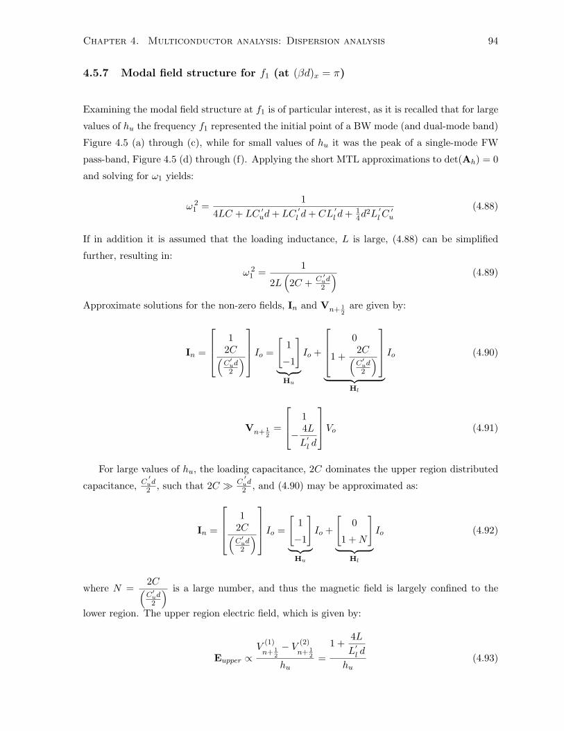
Chapter 4. Multiconductor analysis: Dispersion analysis 94
4.5.7 Modal field structure for f1 (at (βd)x = π)
Examining the modal field structure at f1 is of particular interest, as it is recalled that for large
values of hu the frequency f1 represented the initial point of a BW mode (and dual-mode band)
Figure 4.5 (a) through (c), while for small values of hu it was the peak of a single-mode FW
pass-band, Figure 4.5 (d) through (f). Applying the short MTL approximations to det(Ah) = 0
and solving for ω1 yields:
ω 21 =
14LC + LC ′ud+ LC
′l d+ CL
′l d+ 1
4d2L′lC′u
(4.88)
If in addition it is assumed that the loading inductance, L is large, (4.88) can be simplified
further, resulting in:
ω 21 =
1
2L(
2C + C ′ud2
) (4.89)
Approximate solutions for the non-zero fields, In and Vn+ 12
are given by:
In =
12C(C′ud2
) Io =
[1
−1
]︸ ︷︷ ︸
Hu
Io +
0
1 +2C(C′ud2
)
︸ ︷︷ ︸Hl
Io (4.90)
Vn+ 12
=
1
− 4LL′l d
Vo (4.91)
For large values of hu, the loading capacitance, 2C dominates the upper region distributed
capacitance, C′ud2 , such that 2C C
′ud2 , and (4.90) may be approximated as:
In =
12C(C′ud2
) Io =
[1
−1
]︸ ︷︷ ︸
Hu
Io +
[0
1 +N
]︸ ︷︷ ︸
Hl
Io (4.92)
where N =2C(C′ud2
) is a large number, and thus the magnetic field is largely confined to the
lower region. The upper region electric field, which is given by:
Eupper ∝V
(1)
n+ 12
− V (2)
n+ 12
hu=
1 +4LL′l d
hu(4.93)
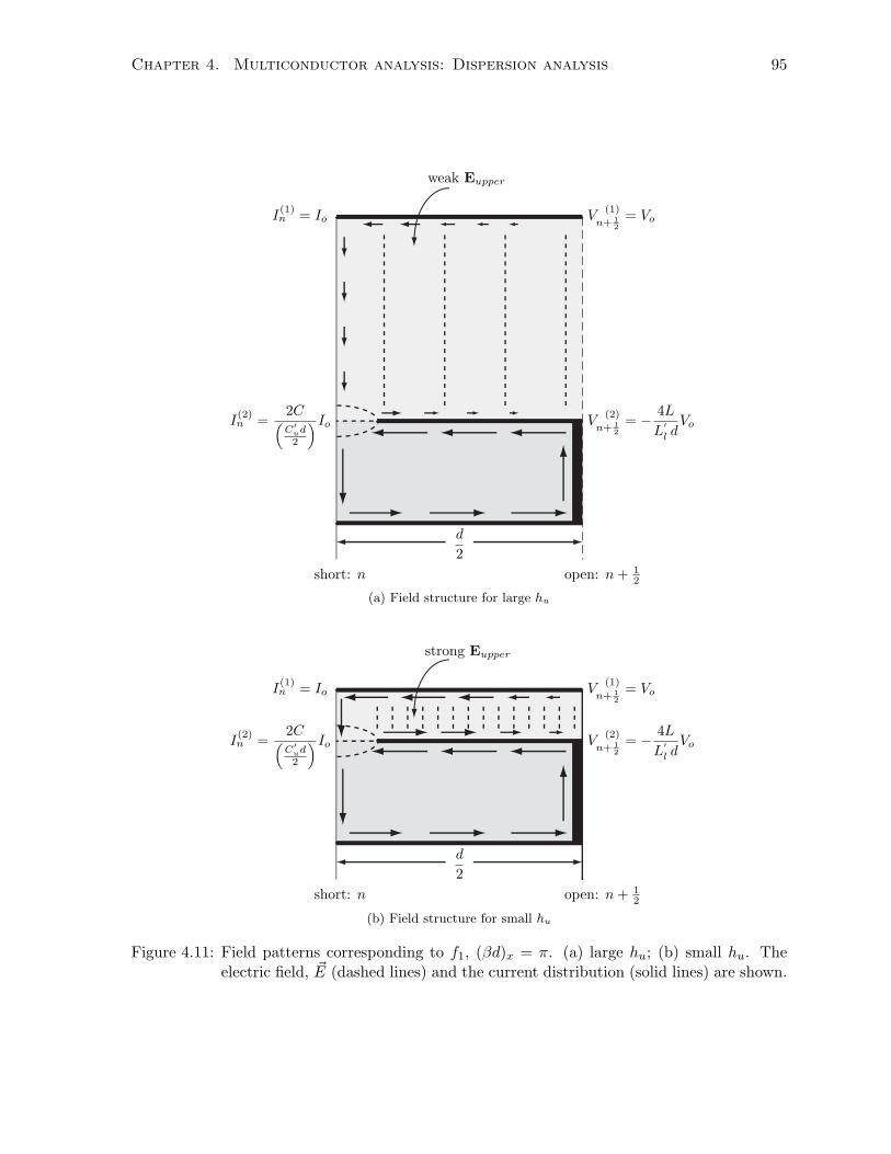
Chapter 4. Multiconductor analysis: Dispersion analysis 95
short: n open: n + 12
d
2
I(1)n = Io
I(2)n =
2C(C′
ud2
)Io
V(1)
n+ 12
= Vo
V(2)
n+ 12
= − 4L
L′l d
Vo
weak Eupper
(a) Field structure for large hu
short: n open: n + 12
d
2
I(1)n = Io
I(2)n =
2C(C′
ud2
)Io
V(1)
n+ 12
= Vo
V(2)
n+ 12
= − 4L
L′l d
Vo
strong Eupper
(b) Field structure for small hu
Figure 4.11: Field patterns corresponding to f1, (βd)x = π. (a) large hu; (b) small hu. Theelectric field, ~E (dashed lines) and the current distribution (solid lines) are shown.
Chapter 4. Multiconductor analysis: Dispersion analysis 96
is relatively weak, and hence both the magnetic and electric fields are largely confined to the
lower region. When 2C C′ud2 (4.89) can be further approximated, resulting in:
ω 21 =
14LC
(4.94)
which represents a resonance between the loading inductance, 2L, and the loading capacitance,
2C and is indicative of the commencement of a BW band, as noted in Section 1.2.2. The
approximate field structure for this case (relatively large hu) is shown in Figure 4.11a.
Conversely for small hu, C′ud2 dominates 2C, so that
2C(C′ud2
) → 0, allowing In to be approx-
imated as:
In =
12C(C′ud2
) Io =
[1
−1
]︸ ︷︷ ︸
Hu
Io +
[0
1
]︸︷︷︸Hl
Io (4.95)
from which it is apparent that the magnetic field permeates both regions with equal strength.
Additionally, for small hu, upper region electric field, (4.93) is large, causing a significant
displacement current to be generated in the upper region, as depicted in Figure 4.11b. Thus for
small upper region height, hu, the impedance due to the upper region distributed capacitance,C′ud2 is smaller than that due to the loading capacitance, 2C, and a majority of the displacement
current travels through the upper region, rather than through 2C. In this case the resonant
frequency, (4.89) may be approximated as:
ω 21 =
1LC ′ud
(4.96)
That a BW mode does not commence at f1 for small hu is due to the fact that the fields are
no longer confined to the lower region of the geometry, and hence the fringing capacitance,
2C, which is associated with the backward wave mode, is weakly excited relative to the upper
region parallel plate capacitance, Cud2 . Additionally, from (4.96) it is apparent that as hu → 0,
f1 → 0 indicating that the bandwidth of the lowest pass-band becomes arbitrarily small.
4.6 Design considerations
Up until this point the alteration of the dispersion curves of the shielded Sievenpiper structure
were observed under the variation of a single parameter alone, hu the upper region height, with
all other geometric and electrical parameters held fixed. This was done so as to simplify the
presentation, although to achieve a desired response many other parameters may be altered.
Tailoring of the dispersion can be achieved by examining the frequencies f1 through f4, which
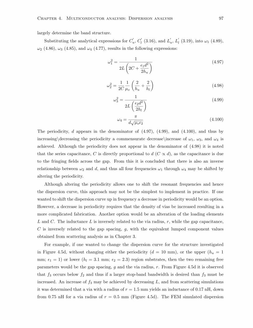
Chapter 4. Multiconductor analysis: Dispersion analysis 97
largely determine the band structure.
Substituting the analytical expressions for C′u, C
′l (3.16), and L
′u, L
′l (3.19), into ω1 (4.89),
ω2 (4.86), ω3 (4.85), and ω4 (4.77), results in the following expressions:
ω21 =
1
2L(
2C +ε1d
2
2hu
) (4.97)
ω22 =
12C
1µo
(2hu
+2hl
)(4.98)
ω23 =
1
2L(ε2d
2
2hl
) (4.99)
ω4 =π
d√µoε2
(4.100)
The periodicity, d appears in the denominator of (4.97), (4.99), and (4.100), and thus by
increasing\decreasing the periodicity a commensurate decrease\increase of ω1, ω3, and ω4 is
achieved. Although the periodicity does not appear in the denominator of (4.98) it is noted
that the series capacitance, C is directly proportional to d (C ∝ d), as the capacitance is due
to the fringing fields across the gap. From this it is concluded that there is also an inverse
relationship between ω2 and d, and thus all four frequencies ω1 through ω4 may be shifted by
altering the periodicity.
Although altering the periodicity allows one to shift the resonant frequencies and hence
the dispersion curve, this approach may not be the simplest to implement in practice. If one
wanted to shift the dispersion curve up in frequency a decrease in periodicity would be an option.
However, a decrease in periodicity requires that the density of vias be increased resulting in a
more complicated fabrication. Another option would be an alteration of the loading elements
L and C. The inductance L is inversely related to the via radius, r, while the gap capacitance,
C is inversely related to the gap spacing, g, with the equivalent lumped component values
obtained from scattering analysis as in Chapter 3.
For example, if one wanted to change the dispersion curve for the structure investigated
in Figure 4.5d, without changing either the periodicity (d = 10 mm), or the upper (hu = 1
mm; ε1 = 1) or lower (hl = 3.1 mm; ε2 = 2.3) region substrates, then the two remaining free
parameters would be the gap spacing, g and the via radius, r. From Figure 4.5d it is observed
that f3 occurs below f2 and thus if a larger stop-band bandwidth is desired than f3 must be
increased. An increase of f3 may be achieved by decreasing L, and from scattering simulations
it was determined that a via with a radius of r = 1.5 mm yields an inductance of 0.17 nH, down
from 0.75 nH for a via radius of r = 0.5 mm (Figure 4.5d). The FEM simulated dispersion
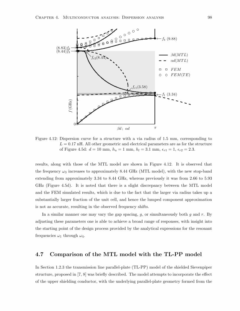
Chapter 4. Multiconductor analysis: Dispersion analysis 98
Figure 4.12: Dispersion curve for a structure with a via radius of 1.5 mm, corresponding toL = 0.17 nH. All other geometric and electrical parameters are as for the structureof Figure 4.5d: d = 10 mm, hu = 1 mm, hl = 3.1 mm, εr1 = 1, εr2 = 2.3.
results, along with those of the MTL model are shown in Figure 4.12. It is observed that
the frequency ω3 increases to approximately 8.44 GHz (MTL model), with the new stop-band
extending from approximately 3.34 to 8.44 GHz, whereas previously it was from 2.66 to 5.93
GHz (Figure 4.5d). It is noted that there is a slight discrepancy between the MTL model
and the FEM simulated results, which is due to the fact that the larger via radius takes up a
substantially larger fraction of the unit cell, and hence the lumped component approximation
is not as accurate, resulting in the observed frequency shifts.
In a similar manner one may vary the gap spacing, g, or simultaneously both g and r. By
adjusting these parameters one is able to achieve a broad range of responses, with insight into
the starting point of the design process provided by the analytical expressions for the resonant
frequencies ω1 through ω4.
4.7 Comparison of the MTL model with the TL-PP model
In Section 1.2.3 the transmission line parallel-plate (TL-PP) model of the shielded Sievenpiper
structure, proposed in [7, 8] was briefly described. The model attempts to incorporate the effect
of the upper shielding conductor, with the underlying parallel-plate geometry formed from the

Chapter 4. Multiconductor analysis: Dispersion analysis 99
n
n
n + 1
n + 1
Y
Y
Lo = L
Co = C′ud
hu, ǫ1
hl, ǫ2
Zo =
√L′(TL-PP)C ′(TL-PP)
Zo Zo
w
d
2d
2
d
Shielding plane
ground plane
(a) Unloaded 2 conductor TL-PP (b) Transformation into a loaded TL-PP structure
(c) Equivalent TL-PP circuit (d) Loading admittance, Y
Figure 4.13: Envisioning the shielded Sievenpiper structure as a 2-conductor parallel-platetransmission line (TL) upon which the patches and vias act as loading elements.The underlying unloaded TL consists of the shielding plane and the ground planeas depicted in (a), which is transformed to the actual (loaded) structure in (b).Equivalent circuit for this point of view is shown in (c). Reactive loading elementshown in (d).
shielding conductor and the ground conductor. This is in contrast to the TL(BW) model of the
unshielded Sievenpiper structure, introduced in Section 1.2.2, which does not incorporate the
upper shielding conductor. In this section the TL-PP model will be examined and compared
with both the FEM simulations and the MTL model.
The proposed equivalent circuit for the TL-PP model, along with the underlying parallel-
plate environment of the shielded structure are shown in Figure 4.13. It is observed that the
underlying geometry is that of a parallel-plate TL formed from the shielding conductor and
the ground conductor, with per-unit-length parameters, L′(TL-PP) and C ′(TL-PP). These
parameters can be written in terms of the components of the per-unit-length capacitance and
inductance matrices, C′ (3.16) and L′ (3.19), which define the unloaded MTL geometry, and
are given by:
C′(TL-PP) =
C′uC
′l
C ′u + C′l
(4.101)
L′(TL-PP) = L
′u + L
′l (4.102)
The loading is modeled as a shunt admittance, Y , formed from the series combination of the
capacitance, Co = C′ud (due to the parallel-plate capacitance between the patch layer and the
Chapter 4. Multiconductor analysis: Dispersion analysis 100
shield), and the inductance, Lo = L (due to the via). It is noted that the fringing capacitance,
C, of the MTL model, is not accounted for in the TL-PP model. The dispersion equation is
given by:
cosh(γd) = Af (4.103)
where
Af = cos(θTL-PP) +12jZoY sin(θTL-PP) (4.104)
with
θTL-PP = ωd√L′(TL-PP)C ′(TL-PP), (4.105)
Zo =
√L′(TL-PP)C ′(TL-PP)
(4.106)
and
Y =jωCo
1− ω2LoCo(4.107)
The dispersion equation (4.103) can only account for a single mode of propagation, and hence
unlike the MTL model is incapable of capturing the dual-mode behaviour of the shielded struc-
ture for large values of hu. However, even for relatively small values of hu the TL-PP model
greatly overestimates the bandwidth of the stop-band. In Figure 4.14, FEM generated dis-
persion curves are compared with those obtained from (4.103). Two simulations are shown,
with upper region height, hu having the values 0.2 mm and 1 mm. All of the other geometric
and electrical parameters are identical to those used to generate the dispersion curves from
Figure 4.5. The stop-band predicted by the TL-PP model is shaded in these figures. For both
hu = 0.2 mm and hu = 1 mm the first pass-band contains a single FW mode. With hu = 0.2
mm the peak of the first pass-band, at f1 = 1.78 GHz is accurately predicted by the TL-PP
model; however for hu = 1 mm the frequency f1(TL-PP) = 3.64 GHz obtained from the TL-PP
model is approximately 35% greater than that given by the FEM simulation, f1 (FEM) = 2.66
GHz.
The FEM simulations show that the peak of the first stop-band occurs at f3 (FEM) = 5.93
GHz for both hu = 0.2 mm and 1 mm, as was captured by the MTL model (Figures 4.5:d,f).
However the TL-PP model overpredicts the peak of the stop-band in both cases; for hu = 0.2
mm, the peak predicted by the TL-PP model is at f3 (TL-PP) = 6.68 GHz (12.5% greater),
while for hu = 1 mm the peak occurs at f3 (TL-PP) = 8.83 GHz (48.9% greater). This shows
that even for cases where the dispersion is single mode, the TL-PP model does not accurately
predict the band-edges. Additionally, it is noted that the TL-PP model cannot capture complex
modes within the stop-band, as obtained from the MTL analysis.
Approximate analytical formulas for the resonant frequencies ω1 and ω3 obtained from the
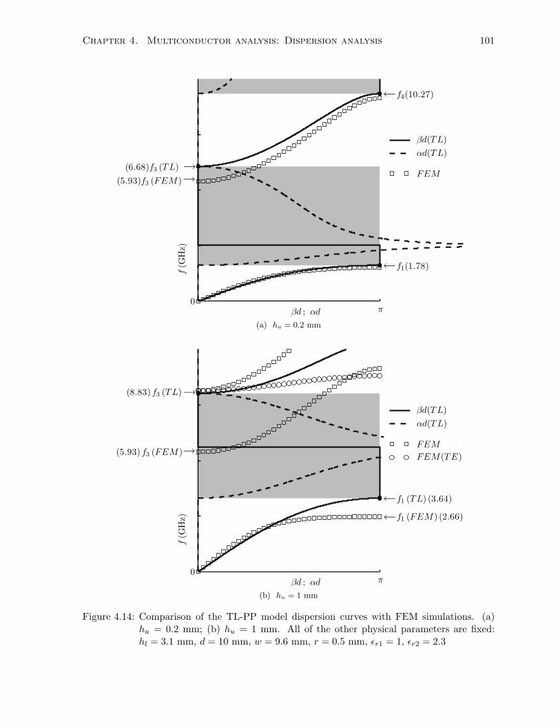
Chapter 4. Multiconductor analysis: Dispersion analysis 101
(a) hu = 0.2 mm
(b) hu = 1 mm
Figure 4.14: Comparison of the TL-PP model dispersion curves with FEM simulations. (a)hu = 0.2 mm; (b) hu = 1 mm. All of the other physical parameters are fixed:hl = 3.1 mm, d = 10 mm, w = 9.6 mm, r = 0.5 mm, εr1 = 1, εr2 = 2.3
Chapter 4. Multiconductor analysis: Dispersion analysis 102
TL-PP dispersion (4.103) are given by:
ω21 (TL-PP) =
1LC ′ud+ 1
4L′ld
2C ′u + 14L′ud
2C ′u(4.108)
and
ω23 (TL-PP) =
1L
(2C ′ud
+1C′l d
)(4.109)
The expression for ω21 (TL-PP) (4.108) converges to that obtained from the MTL analysis (4.96),
in the limit hu → 0, which shows that the peak of the first pass-band, predicted by the TL-PP
model converges to that of the MTL model for small upper region height, hu. However, for
larger upper region height, the TL-PP formula (4.108) greatly overestimates that obtained from
the MTL model in the same limit, (4.94), ω21 (MTL) = 1
4LC , which is a function of the series
fringing capacitance, C of the MTL model. As the TL-PP model does not include the fringing
capacitance, it is incorrect in this limit. However, even more fundamentally, for large hu, the
frequency f1 is the commencement of dual-mode pass-band, which the TL-PP model cannot
capture.
The expression for ω23 (TL-PP) (4.109) is a function of both the upper and lower region
geometries, and does not account for the invariance of f3 when hl is fixed. The expression for
ω23 (MTL) (4.85) correctly accounts for the fact that f3 is only a function of the lower region
geometry. Comparing (4.109) and (4.85) shows that:
ω23 (TL-PP) =
1L
(2C ′ud
+1C′l d
)≥ 1LC
′l d
= ω23 (MTL) (4.110)
and hence the peak of the stop-band predicted by the TL-PP model, ω23 (TL-PP), is always
larger than that of the MTL model, ω23 (MTL), leading to the overestimation of the stop-band
bandwidth. Only in the limit hu → 0 do the two models converge with ω23 (TL-PP)→ ω2
3 (MTL)
in that case. Thus, both ω21 (TL-PP) and ω2
3 (TL-PP) converge to the correct expressions
obtained from MTL analysis only in the limit of very small upper region height.
4.8 Modal degeneracy at f2
The FEM dispersion simulations from Figure 4.5 revealed that two modes emerged from the
resonance frequency, f2, which occurs at (βd)x = 0. One mode was captured by the MTL
model, and the other was not.
In Section 4.5 it was determined that the condition (βd)x = 0 corresponds to the boundary
conditions, O:O:O or S:S:S at nodes n : n+ 12 : n+ 1, where O and S stand for open or short
circuits. These condition imply H-walls or E-walls at the corresponding nodes: H:H:H or E:E:E.
Chapter 4. Multiconductor analysis: Dispersion analysis 103
Although these conditions were obtained for the unit cell along the longitudinal (propagation)
direction, x, due to the symmetry of the structure it is apparent that the transverse boundary
conditions corresponding to the phase shift (βd)y = 0 also would have to conform to the same
conditions. The MTL model assumed that the transverse walls were described by H-walls.
However due to the symmetry of the structure the fact that the central bisecting plane acted
as an H-wall was automatically incorporated, as is shown in Figure 4.15 (a).
For the case were the transverse boundary conditions are E:E:E, as shown in Figure 4.15 (b),
it is observed that the structure becomes electrically connected. Such a geometry does not
support quasi-TEM modes, and thus the MTL model cannot capture the mode corresponding to
E:E:E boundary conditions, which was TE. The top view of the transverse and central boundary
conditions corresponding to the frequency f2 are shown in Figure 4.15 (c) and (d). Due to
symmetry, both configurations correspond to the same frequency. However with (βd)y = 0 fixed,
only the boundary conditions shown in Figure 4.15 (c) are captured by the MTL model, for
values of (βd)x 6= 0; that is when propagation along the x-direction is assumed. In conclusion,
it is noted that even though the MTL model does not account for the dispersion of the TE
mode, the fact that a modal degeneracy occurs at f2 is predicted by the MTL analysis.
4.9 Summary
In this chapter a periodic multiconductor transmission line (MTL) model of the shielded Sieven-
piper structure was developed. Initially, a periodic unit cell, composed of a cascade of lumped
components and sections of MTL lines was presented, with a corresponding dispersion equation
derived from it.
By applying suitable approximations to the full periodic dispersion equation, a simplified
dispersion equation, in which the effect of the loading elements was incorporated directly into
the per-unit-length MTL parameters, was obtained and analyzed. The simplified dispersion
equation yields simple formulas relating the band-edge frequencies f2 and f3 (which occur
at (βd)y = 0) to the geometry of the structure and the loading elements. Additionally, a
frequency band between fc1 and fc2 supporting complex modes was shown to exist, with some
of the properties of complex modes reviewed.
The fully periodic MTL model was subsequently returned to, supplementing the deficiencies
of the the simplified model. The fully periodic dispersion equation was shown to have excellent
correspondence with FEM simulations, over a broad range of geometric parameters of the
structure. Additionally, the fully periodic model was able to capture the two additional band
edge frequencies, f1 and f4, which occur at (βd)x = π. Equivalent circuits, analytical formulas,
and modal eigenvectors corresponding to the band-edges were obtained. These results were

Chapter 4. Multiconductor analysis: Dispersion analysis 104
(βd)x = 0(βd)x = 0
(βd)y = 0(βd)y = 0
x
y
y
z
(a) Side view (MTL) (b) Side view (TE)
(c) Top view, as seenbelow the Shielding conductor (MTL)
(d) Top view, as seenbelow the Shielding conductor (TE)
nn n + 12n + 1
2 n + 1n + 1
H-walls
E-walls
Figure 4.15: Boundary conditions corresponding to the two degenerate modes at f2: (a) Trans-verse boundary conditions for the mode described by MTL theory. (b) Transverseboundary conditions for the TE mode. (c) Boundary conditions at the transverse(y) walls, and longitudinal (x) walls for the MTL mode. (d) Boundary conditionsfor the TE mode are switched compared with (c)

Chapter 4. Multiconductor analysis: Dispersion analysis 105
particulary important in revealing the physical mechanism underlying the qualitative change
in behaviour (dual-mode to single-mode dispersion) of the structure as the upper region height
is decreased from large to small values. Finally, using the band-edge equivalent circuits, the
modal degeneracy which occurs at f2 was explained.
Chapter 5
Slow Wave Analysis
5.1 Introduction
The dispersion analysis of the shielded structure developed in Chapter 4 revealed that in the
limit ω → 0 the structure supported a FW mode commencing at DC. Modal plots from Chap-
ter 2 revealed that the field structure had an asymmetric distribution: The electric field in the
upper region was nearly constant, Eu = Eo, while in the lower region the electric field was
virtually zero, El ≈ 0. The magnetic field however was virtually constant throughout both the
upper and lower regions, Hu ≈ Hl = Ho. For relatively large shield-patch distances, corre-
sponding to large hu the degree of slowing was minimal, but as the shielding conductor was
brought closer to the patch layer significant slowing was achievable.
In this chapter the low frequency limit for both the propagation constant and the modal
eigenvectors will be determined using the MTL analysis. Interestingly, in this limit, the prop-
agation constant, βd will be seen to be independent of the value of the loading elements, L
and C, and only depend on a subset of the parameters defining the underlying MTL geometry,
Cu′, Cl ′, L
′u, and L
′l. The analysis shows that the degree of the slow-wave effect is controlled
by the distance between the shielding conductor and the patch (mushroom) layer, hu, with a
significant slowing of the mode possible as the aforementioned distance is decreased. A physical
explanation of this phenomenon is arrived at by examining the corresponding low frequency
modal eigenvector. The fact that the low frequency dispersion is independent of L and C does
not imply that they are not needed to achieve the slow wave effect. To confirm the necessity
of the simultaneous presence of both L and C in achieving the effect, two related structures
will be considered: First, a structure with the loading capacitance removed (shorted out), cor-
responding to C → ∞, and subsequently a structure with the loading inductance removed,
corresponding to L → ∞. Propagation constants and modal eigenvectors for each of these
separate structures will be calculated, showing that the slow wave effect is lost, thus proving
106
Chapter 5. Slow Wave Analysis 107
the necessity of both L and C, and further enhancing the physical picture developed for the
shielded structure. The theory is compared with full-wave finite element simulations, with
excellent correspondence between the two observed.
5.2 MTL model
The dispersion equation for the shielded structure (4.20) is a quadratic in the variable, cosh(γd),
corresponding to two independent modes of propagation. In the low frequency limit a Taylor
expansion may be performed on (4.20). One mode is evanescent, which corresponds to a
backward wave (BW) mode below cut-off, while the other mode, which is the mode under
consideration now, is a forward wave (FW) mode, which extends to DC. In the limit ω → 0 the
dispersion of the FW mode is given by:
(βd)2LC = d2C′u
(L′u + L
′l
)ω2 +
d3(C(L
′l)
2C′u + LL
′u(C
′u)2 + L(C
′u)2L
′l
)ω4 + · · · (5.1)
where the subscript LC of (βd)LC denotes the fact the dispersion equation is for the actual
shielded structure, which has both a loading L and a loading C, in contrast to related structures
which will be analyzed later in this chapter, where one of the loading elements is eliminated.
When (βd)LC 1 the dispersion (5.1), is well approximated by considering only the first term
in the series expansion, resulting in the following low frequency (linear) dispersion curve:
βLC =√C ′u(L′u + L
′l)ω (5.2)
which represents a forward wave with group, vg, and phase velocity, vφ, equal to each other and
given by:
vφ(LC) = vg(LC) =1√
C ′u(L′u + L′l)
(5.3)
In the limit hu → 0, C′u →∞, while the term L
′u +L
′l remains finite, so that vg → 0 as hu → 0.
The group velocity is thus bounded below only by zero, and can be made arbitrarily small:
0 ≤ vg(LC) ≤ 1√C ′uL
′u
(5.4)
From (5.3) the resulting mode has an effective capacitance and inductance per-unit-length
given by:
C′eff (LC) = C
′u (5.5)

Chapter 5. Slow Wave Analysis 108
L′eff (LC) = L
′u + L
′l (5.6)
The low frequency phase velocity is independent of the loading elements L and C, and depends
only on the electrical and geometric parameters of the upper and lower regions. However,
the electrical parameters appear in an asymmetrical manner, with the effective inductance,
L′eff (LC) = L
′u + L
′l involving both the upper and lower region geometry, while the effective
capacitance, C′eff (LC) = C
′u involves only the upper region geometry. A similar phenomenon
was observed in [10], where a slow wave effect was achieved by utilizing a two-dimensional
array of metallic posts. The slow wave effect can be understood as being due to a capacitance
enhancement, and this is most readily seen by considering the propagation on a commensurate
two conductor geometry which is identical to the shielded structure, but with the entire patch
layer (Conductor 2) and the via removed. Such a structure is depicted in Figure 5.1, with the
figure indicating the equal and opposite currents on the two conductors as is expected for a two
conductor geometry, and non-zero fields, in both the upper and lower regions. This structure
is a simple two conductor transmission line (TL) with dispersion given by:
(βd)2TL = d2
(C′uC′l
C ′u + C′l
)︸ ︷︷ ︸
C′eff
(L′u + L
′l
)︸ ︷︷ ︸L′eff
ω2 (5.7)
and whose per-unit length capacitance, C′(TL) and inductance L
′(TL) can be written in
terms of the components of the capacitance and inductance matrices characterizing the shielded
structure:
C′(TL) =
C′uC
′l
C ′u + C′l
(5.8)
L′(TL) = L
′u + L
′l (5.9)
The effective inductance L′eff (LC) = L
′u+L
′l (5.6), of the FW mode for the shielded mushroom
structure is identical to the inductance of the the commensurate (2-conductor) geometry, L′(TL)
(5.9), consisting of the upper shielding conductor and the ground conductor alone. However, the
per-unit length effective capacitance of the shielded structure, C′eff (LC) (5.5) is always greater
than that of the commensurate TL geometry, C′(TL) (5.8), as can be shown by computing
their ratio,
rC =C′eff (LC)
C ′(TL)= 1 +
ε1 hlε2 hu
> 1 (5.10)
which is always greater than 1 and hence a capacitance enhancement has been achieved. Even
in the case where the relative permittivities of the upper and lower regions are equal to one,
ε1 = ε2 = εo, is the ratio rC(ε1 = ε2 = εo) = 1 + hlhu
> 1. Thus obtaining the slow wave effect
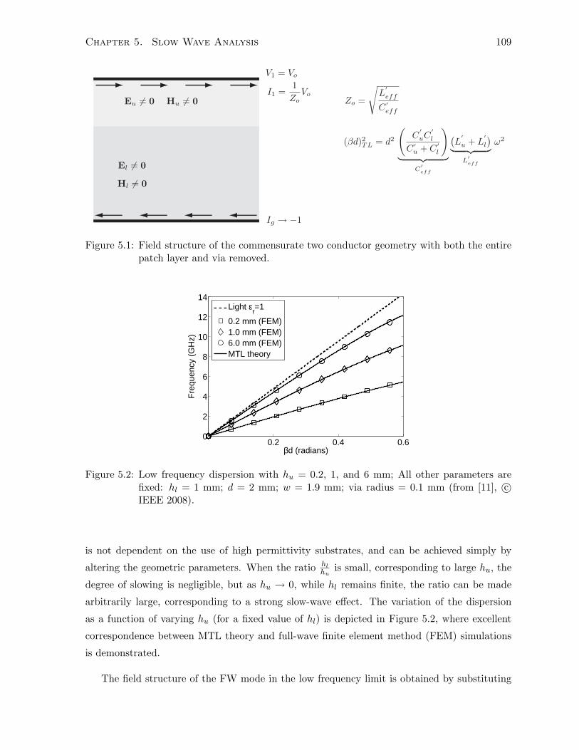
Chapter 5. Slow Wave Analysis 109
V1 = Vo
I1 =1Zo
Vo
Ig → −1
(βd)2TL = d2
(C
′uC
′l
C ′u + C
′l
)︸ ︷︷ ︸
C′eff
(L
′u + L
′l
)︸ ︷︷ ︸L
′eff
ω2
Zo =
√L
′eff
C′eff
Hu 6= 0
Hl 6= 0
Eu 6= 0
El 6= 0
Figure 5.1: Field structure of the commensurate two conductor geometry with both the entirepatch layer and via removed.
0.2 0.4 0.60
2
4
6
8
10
12
14
βd (radians)
Fre
quen
cy (
GH
z)
Light εr=1
0.2 mm (FEM)1.0 mm (FEM)6.0 mm (FEM)MTL theory
Figure 5.2: Low frequency dispersion with hu = 0.2, 1, and 6 mm; All other parameters arefixed: hl = 1 mm; d = 2 mm; w = 1.9 mm; via radius = 0.1 mm (from [11], c©IEEE 2008).
is not dependent on the use of high permittivity substrates, and can be achieved simply by
altering the geometric parameters. When the ratio hlhu
is small, corresponding to large hu, the
degree of slowing is negligible, but as hu → 0, while hl remains finite, the ratio can be made
arbitrarily large, corresponding to a strong slow-wave effect. The variation of the dispersion
as a function of varying hu (for a fixed value of hl) is depicted in Figure 5.2, where excellent
correspondence between MTL theory and full-wave finite element method (FEM) simulations
is demonstrated.
The field structure of the FW mode in the low frequency limit is obtained by substituting
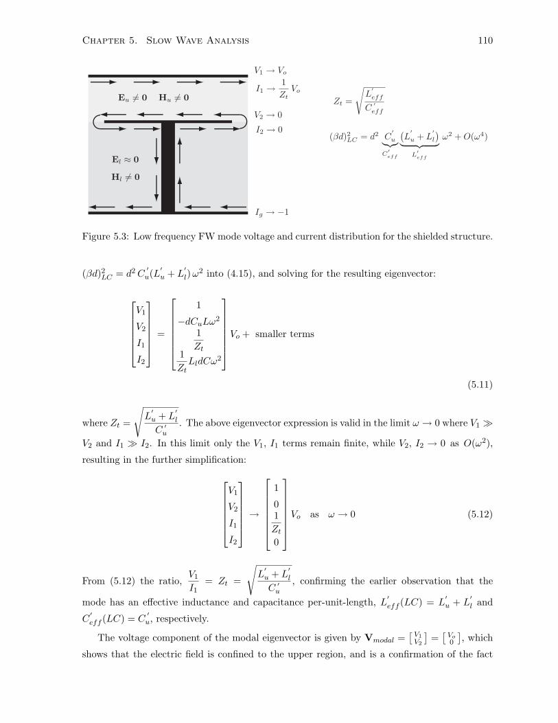
Chapter 5. Slow Wave Analysis 110
V1 → Vo
V2 → 0
I1 → 1Zt
Vo
I2 → 0
Ig → −1
(βd)2LC = d2 C′u︸︷︷︸
C′eff
(L
′u + L
′l
)︸ ︷︷ ︸L
′eff
ω2 + O(ω4)
Zt =
√L
′eff
C′eff
Hu 6= 0
Hl 6= 0
Eu 6= 0
El ≈ 0
Figure 5.3: Low frequency FW mode voltage and current distribution for the shielded structure.
(βd)2LC = d2C′u(L
′u + L
′l)ω
2 into (4.15), and solving for the resulting eigenvector:
V1
V2
I1
I2
=
1
−dCuLω2
1Zt
1ZtLldCω
2
Vo + smaller terms
(5.11)
where Zt =
√L′u + L
′l
C ′u. The above eigenvector expression is valid in the limit ω → 0 where V1
V2 and I1 I2. In this limit only the V1, I1 terms remain finite, while V2, I2 → 0 as O(ω2),
resulting in the further simplification:
V1
V2
I1
I2
→
1
01Zt0
Vo as ω → 0 (5.12)
From (5.12) the ratio,V1
I1= Zt =
√L′u + L
′l
C ′u, confirming the earlier observation that the
mode has an effective inductance and capacitance per-unit-length, L′eff (LC) = L
′u + L
′l and
C′eff (LC) = C
′u, respectively.
The voltage component of the modal eigenvector is given by Vmodal =[V1V2
]=[Vo0
], which
shows that the electric field is confined to the upper region, and is a confirmation of the fact
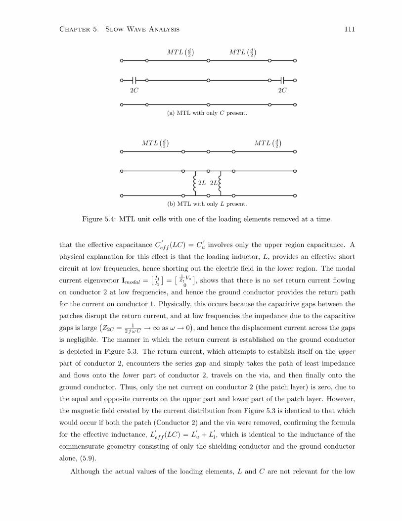
Chapter 5. Slow Wave Analysis 111
2C2C
MTL(
d2
)MTL
(d2
)
(a) MTL with only C present.
2L2L
MTL(
d2
)MTL
(d2
)
(b) MTL with only L present.
Figure 5.4: MTL unit cells with one of the loading elements removed at a time.
that the effective capacitance C′eff (LC) = C
′u involves only the upper region capacitance. A
physical explanation for this effect is that the loading inductor, L, provides an effective short
circuit at low frequencies, hence shorting out the electric field in the lower region. The modal
current eigenvector Imodal =[I1I2
]=[ 1ZtVo
0
], shows that there is no net return current flowing
on conductor 2 at low frequencies, and hence the ground conductor provides the return path
for the current on conductor 1. Physically, this occurs because the capacitive gaps between the
patches disrupt the return current, and at low frequencies the impedance due to the capacitive
gaps is large(Z2C = 1
2 j ω C →∞ as ω → 0), and hence the displacement current across the gaps
is negligible. The manner in which the return current is established on the ground conductor
is depicted in Figure 5.3. The return current, which attempts to establish itself on the upper
part of conductor 2, encounters the series gap and simply takes the path of least impedance
and flows onto the lower part of conductor 2, travels on the via, and then finally onto the
ground conductor. Thus, only the net current on conductor 2 (the patch layer) is zero, due to
the equal and opposite currents on the upper part and lower part of the patch layer. However,
the magnetic field created by the current distribution from Figure 5.3 is identical to that which
would occur if both the patch (Conductor 2) and the via were removed, confirming the formula
for the effective inductance, L′eff (LC) = L
′u + L
′l, which is identical to the inductance of the
commensurate geometry consisting of only the shielding conductor and the ground conductor
alone, (5.9).
Although the actual values of the loading elements, L and C are not relevant for the low
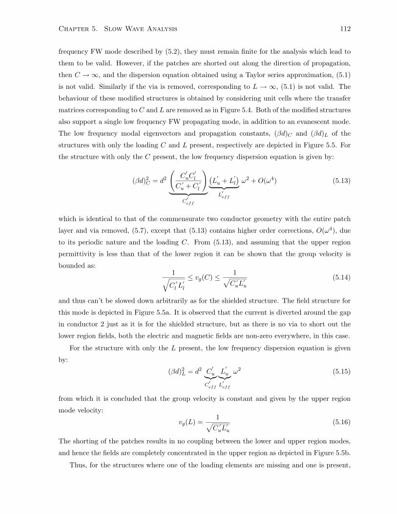
Chapter 5. Slow Wave Analysis 112
frequency FW mode described by (5.2), they must remain finite for the analysis which lead to
them to be valid. However, if the patches are shorted out along the direction of propagation,
then C →∞, and the dispersion equation obtained using a Taylor series approximation, (5.1)
is not valid. Similarly if the via is removed, corresponding to L → ∞, (5.1) is not valid. The
behaviour of these modified structures is obtained by considering unit cells where the transfer
matrices corresponding to C and L are removed as in Figure 5.4. Both of the modified structures
also support a single low frequency FW propagating mode, in addition to an evanescent mode.
The low frequency modal eigenvectors and propagation constants, (βd)C and (βd)L of the
structures with only the loading C and L present, respectively are depicted in Figure 5.5. For
the structure with only the C present, the low frequency dispersion equation is given by:
(βd)2C = d2
(C′uC′l
C ′u + C′l
)︸ ︷︷ ︸
C′eff
(L′u + L
′l
)︸ ︷︷ ︸L′eff
ω2 +O(ω4) (5.13)
which is identical to that of the commensurate two conductor geometry with the entire patch
layer and via removed, (5.7), except that (5.13) contains higher order corrections, O(ω4), due
to its periodic nature and the loading C. From (5.13), and assuming that the upper region
permittivity is less than that of the lower region it can be shown that the group velocity is
bounded as:1√C′l L′l
≤ vg(C) ≤ 1√C ′uL
′u
(5.14)
and thus can’t be slowed down arbitrarily as for the shielded structure. The field structure for
this mode is depicted in Figure 5.5a. It is observed that the current is diverted around the gap
in conductor 2 just as it is for the shielded structure, but as there is no via to short out the
lower region fields, both the electric and magnetic fields are non-zero everywhere, in this case.
For the structure with only the L present, the low frequency dispersion equation is given
by:
(βd)2L = d2 C′u︸︷︷︸
C′eff
L′u︸︷︷︸
L′eff
ω2 (5.15)
from which it is concluded that the group velocity is constant and given by the upper region
mode velocity:
vg(L) =1√C ′uL
′u
(5.16)
The shorting of the patches results in no coupling between the lower and upper region modes,
and hence the fields are completely concentrated in the upper region as depicted in Figure 5.5b.
Thus, for the structures where one of the loading elements are missing and one is present,

Chapter 5. Slow Wave Analysis 113
V1 → Vo
V2 → V2(6= 0)
I1 → 1Zo
Vo
I2 → 0
Ig → −1
(βd)2C = d2
(C
′uC
′l
C ′u + C
′l
)︸ ︷︷ ︸
C′eff
(L
′u + L
′l
)︸ ︷︷ ︸L
′eff
ω2 + O(ω4)
Zo =
√L
′eff
C′eff
Hu 6= 0
Hl 6= 0
Eu 6= 0
El 6= 0
(a) Voltage and current eigenvectors with only C present.
V1 → Vo
V2 = 0
I1 =1
ZuVo
I2 = − 1Zu
Vo
Ig = 0
(βd)2L = d2 C′u︸︷︷︸
C′eff
L′u︸︷︷︸
L′eff
ω2
Zu =
√L
′eff
C′eff
Hu 6= 0
Hl = 0
Eu 6= 0
El = 0
(b) Voltage and current eigenvectors with only L present.
Figure 5.5: Eigenvectors corresponding to the MTL unit cell with one of L or C removed.
there is a lack of asymmetry in the modal field profile, and it is this lack of asymmetry which
prevents either a capacitive or an inductive enhancement, and thus a slowing of the low fre-
quency FW mode.
5.3 Summary
In this chapter the slow-wave effect produced by the shielded mushroom structure has been
demonstrated analytically using MTL theory, and confirmed with full-wave FEM simulations.
MTL analysis revealed that the low frequency slow-wave effect was due to an enhanced effective
capacitance per-unit-length, which could be made arbitrarily large, while the inductance per-
unit length remained finite. A physical picture of the mechanism behind the slow-wave effect
was also developed. Additionally, even though the low frequency phase velocity was independent

Chapter 5. Slow Wave Analysis 114
of the loading elements, L and C, the necessity of their presence was established by considering
commensurate geometries where each of L and C was removed from the structure.

Chapter 6
Scattering Analysis
6.1 Introduction
In Chapter 4 the dispersion properties of the shielded Sievenpiper structure were analyzed
using MTL theory. By applying a Bloch analysis to a single MTL unit cell, two propagation
constants, (γd)a,b, corresponding to two independent modes of propagation, were derived. For
each propagation constant, which is related to the eigenvalue of the unit cell’s transfer matrix,
Tunit−cell−MTL (4.13), there exists a corresponding modal eigenvector, (4.15),[V, I
]ta,b
, which
reveals a given modes’ field concentration. The MTL theory analysis was shown to have excellent
correspondence with FEM simulations.
In this chapter we will consider the excitation of a finite cascade of unit cells of the shielded
structure, from which generalized scattering parameters will be derived. The dispersion equa-
tion and modal eigenvectors correspond to an (infinite) periodic structure, but in actual physical
applications the structure will of course be finite. The scattering analysis thus provides one
with an understanding of the operation of the shielded structure under realistic situations. A
general excitation will support a superposition of all the Bloch modes, and by examining the
scattering parameters in conjunction with the modal excitation strengths a picture of the oper-
ation of multimodal structures will be developed. In addition, for some finite element method
solvers, it is difficult to obtain the propagation constants in stop-bands (both complex and
evanescent bands). However a scattering simulation can always be performed over all frequen-
cies, and can thus provide confirmation of the propagation constants within both evanescent
mode and complex mode bands. Thus scattering simulations provide an additional way to test
the effectiveness of the MTL analysis. In particular it will be observed that when plotting the
S-parameters as a function of frequency, evanescent mode bands and complex mode bands are
characterized by distinct shapes. For the shielded structure it was seen that both standard
evanescent modes and complex modes are supported, and the distinct signatures of these two
115

Chapter 6. Scattering Analysis 116
types of bands will be observed.
Different forms of excitations will be considered, which are related to different applications of
the structure. Initially, a four-port scattering scenario will be examined, in which the upper and
lower regions of the structure, respectively, are excited separately. Such an excitation is relevant
in the understanding of the operation of the coupled mode coupler developed in [15, 16], where
a compact directional coupler was demonstrated. The operation of such a coupler is directly
related to the existence of complex modes, and in particular the dominant excitation of a single
complex mode. Another application of the four-port scattering analysis is related to 2D NRI
TL grids as developed in [26–28]. It is recalled from Section 1.2.2, that in that work TL theory
was used to model a structure which was fundamentally dual mode, with both a backward
wave (BW) and a forward wave (FW) mode supported. The BW mode was largely confined to
the substrate, while the FW mode was largely situated above the substrate. Multiconductor
transmission line theory can be used to model the dual mode dispersion of such structures. In
particular, by using the MTL model of the shielded structure, it will be shown that a lower
region excitation strongly excites the BW mode, while an upper region excitation generally
excites the FW mode. Additionally, a two-port scattering scenario will be examined. In this
case the excitation is between the shielding conductor and the ground conductor. This type of
excitation is relevant in the operation of the structure as a noise suppression device in digital
circuits [6–8], and as a slot antenna created on the upper shielding conductor [9].
The importance of the scattering analysis may be summarized by the following points:
• Confirmation of the applicability of the periodic Bloch analysis to a more realistic finite
case.
• Confirmation of the propagation constant(s) within the stop-band, including the existence
of complex modes.
• Relates various forms of excitations to structures which support multi-mode/ complex-
mode bands, and their applications.
As mentioned above, different scattering situations will be considered, corresponding to
different input excitations of the cascaded structure. Although the detailed description of
the individual scattering situations will be provided in subsequent sections, the general form
of each analysis may be summarized as follows: A cascade of N unit cells of the shielded
structure is considered, with the Bloch modes obtained from the periodic analysis used as the
basis modes for the cascade. The N unit cell cascade is extended at its input and output
planes by unloaded waveguide sections, for which appropriate port variables will be defined.
The port variables correspond to wave propagation on the unloaded waveguide sections. By
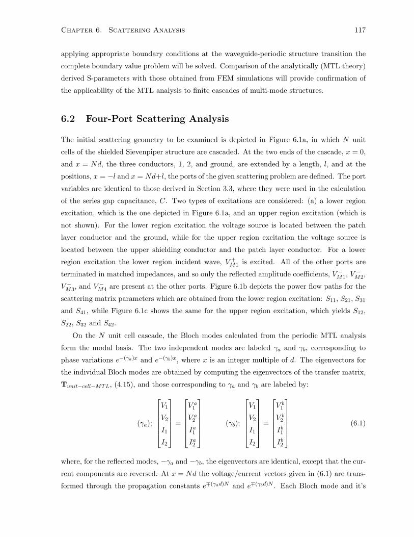
Chapter 6. Scattering Analysis 117
applying appropriate boundary conditions at the waveguide-periodic structure transition the
complete boundary value problem will be solved. Comparison of the analytically (MTL theory)
derived S-parameters with those obtained from FEM simulations will provide confirmation of
the applicability of the MTL analysis to finite cascades of multi-mode structures.
6.2 Four-Port Scattering Analysis
The initial scattering geometry to be examined is depicted in Figure 6.1a, in which N unit
cells of the shielded Sievenpiper structure are cascaded. At the two ends of the cascade, x = 0,
and x = Nd, the three conductors, 1, 2, and ground, are extended by a length, l, and at the
positions, x = −l and x = Nd+l, the ports of the given scattering problem are defined. The port
variables are identical to those derived in Section 3.3, where they were used in the calculation
of the series gap capacitance, C. Two types of excitations are considered: (a) a lower region
excitation, which is the one depicted in Figure 6.1a, and an upper region excitation (which is
not shown). For the lower region excitation the voltage source is located between the patch
layer conductor and the ground, while for the upper region excitation the voltage source is
located between the upper shielding conductor and the patch layer conductor. For a lower
region excitation the lower region incident wave, V +M1 is excited. All of the other ports are
terminated in matched impedances, and so only the reflected amplitude coefficients, V −M1, V −M2,
V −M3, and V −M4 are present at the other ports. Figure 6.1b depicts the power flow paths for the
scattering matrix parameters which are obtained from the lower region excitation: S11, S21, S31
and S41, while Figure 6.1c shows the same for the upper region excitation, which yields S12,
S22, S32 and S42.
On the N unit cell cascade, the Bloch modes calculated from the periodic MTL analysis
form the modal basis. The two independent modes are labeled γa and γb, corresponding to
phase variations e−(γa)x and e−(γb)x, where x is an integer multiple of d. The eigenvectors for
the individual Bloch modes are obtained by computing the eigenvectors of the transfer matrix,
Tunit−cell−MTL, (4.15), and those corresponding to γa and γb are labeled by:
(γa);
V1
V2
I1
I2
=
V a
1
V a2
Ia1
Ia2
(γb);
V1
V2
I1
I2
=
V b
1
V b2
Ib1
Ib2
(6.1)
where, for the reflected modes, −γa and −γb, the eigenvectors are identical, except that the cur-
rent components are reversed. At x = Nd the voltage/current vectors given in (6.1) are trans-
formed through the propagation constants e∓(γad)N and e∓(γbd)N . Each Bloch mode and it’s

Chapter 6. Scattering Analysis 118
Port modes;modal coefficients:V +
M1, V −M1, V −M2
Port modes;modal coefficients:
V −M3, V −M4
Bloch modes;modal coefficients:a+
m, a−m, b+m, b−m
ZuZu
Zl
Zl
vs V +M1
V −M1
V −M2
V −M3
V −M4
cell 1 cell 2 cell N
x = −l x = 0 d 2d Nd x = Nd + l
MTL(
d2
)MTL
(d2
)
L 2C2C
(a)
S11
S21
S31
S41
P1+
P2
P3
P4
(b)
S12
S22
S32
S42
P1
P2+
P3
P4
(c)
Figure 6.1: Four-port scattering: (a) Circuit schematic for the four-port scattering analysiswith lower region excitation; (b) Power flow for lower region excitation; (c) Powerflow for upper region excitation.

Chapter 6. Scattering Analysis 119
reflected counterpart may be excited, with the amplitudes of excitations given by a+m, b
+m, a
−m, b
−m.
For the total system consisting of the port extensions and the cascade of unit cells there are nine
unknown variables in total to be determinedV +M1 , V
−M1 , V
−M2 , V
−M3 , V
−M4 , a
+m, b
+m, a
−m, b
−m
and
hence nine equations are needed to uniquely solve the system.
Due to symmetry, only the excitations of the lower region (mode 1), and the upper region
(mode 2), are required to completely determine the scattering parameters. The steps required
to solve for the scattering parameters for the lower region excitation, S11, S21, S31 and S41 are
given now. The input port plane voltage/current vector (at x = −l) was derived in Section 3.3,
and is given again for convenience:
V1
V2
I1
I2
(x=−l)
=
V +M1 + V −
M1 + V −M2
V +M1 + V −
M1
−V−
M2
ZuV +M1
Zl− V −
M1
Zl+V −M2
Zu
(6.2)
The incident voltage component, V +M1 is solved for by considering the source boundary condi-
tion:
− vs + Zl(I1 + I2) + V2 = 0 (6.3)
Upon substituting the expressions for I1, I2, and V2 from (6.2), V +M1 is solved for from (6.3),
resulting in:
V +M1 =
vs2
(6.4)
The output port plane voltage/current vector (at x = Nd + l) is also identical to that from
Section 3.3, given in (3.44). The transformations of the port variables (at x = −l and x = Nd+l)
to the beginning and end of the MTL unit cell cascade (at x = 0 and x = Nd) are made using

Chapter 6. Scattering Analysis 120
the lower and upper region mode propagation constants, βl and βu, and yield:
V1
V2
I1
I2
(x=0)
=
V +M1 e
−jβll + V −M1 e
jβll + V −M2 e
jβul
V +M1 e
−jβll + V −M1 e
jβll
−V−
M2
Zuejβul
V +M1
Zle−jβll − V −
M1
Zlejβll +
V −M2
Zuejβul
(6.5)
V1
V2
I1
I2
(x=Nd)
=
V −M3 e
jβll + V −M4 e
jβul
V −M3 e
jβll
V −M4
Zuejβul
V −M3
Zle−jβll − V −
M4
Zuejβul
(6.6)
A system of 8 equations in the 8 unknowns,V −M1 , V
−M2 , V
−M3 , V
−M4 , a
+m, b
+m, a
−m, b
−m
is obtained
by imposing continuity of both the voltage and current on conductors 1 and 2, using (6.1), (6.5),
(6.6), at x = 0 and x = Nd, resulting in:
[M11 M12
M21 M22
][VP
BP
]=
[Vs
0
](6.7)
where
M11 =
−ejβll ejβul 0 0
−ejβll 0 0 0
0 ejβul
Zu0 0
ejβll
Zl− ejβul
Zu0 0
M12 =
V a
1 V b1 V a
1 V b1
V a2 V b
2 V a2 V b
2
Ia1 Ib1 −Ia1 −Ib1Ia2 Ib2 −Ia2 −Ib2
(6.8)
M21 =
0 0 −ejβll −ejβul0 0 −ejβll 0
0 0 0 − ejβul
Zu
0 0 − ejβll
Zlejβul
Zu
(6.9)
M22 =
V a
1 e−(γad)N V b
1 e−(γbd)N V a
1 e(γad)N V b
1 e(γbd)N
V a2 e−(γad)N V b
2 e−(γbd)N V a
2 e(γad)N V b
2 e(γbd)N
Ia1 e−(γad)N Ib1e
−(γbd)N −Ia1 e(γad)N −Ib1e(γbd)NIa2 e−(γad)N Ib2e
−(γad)N −Ia2 e(γad)N −Ib2e(γbd)N
(6.10)
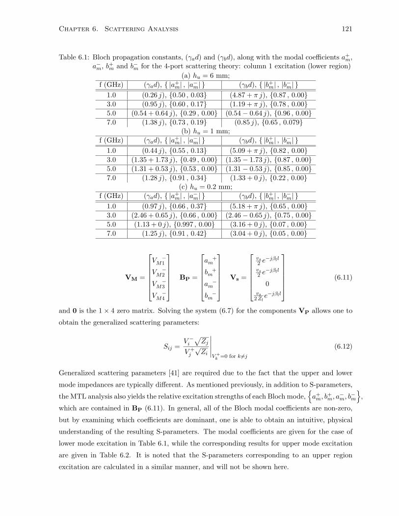
Chapter 6. Scattering Analysis 121
Table 6.1: Bloch propagation constants, (γad) and (γbd), along with the modal coefficients a+m,
a−m, b+m and b−m for the 4-port scattering theory: column 1 excitation (lower region)(a) hu = 6 mm;
f (GHz) (γad), |a+m| , |a−m| (γbd), |b+m| , |b−m|
1.0 (0.26 j), 0.50 , 0.03 (4.87 + π j), 0.87 , 0.003.0 (0.95 j), 0.60 , 0.17 (1.19 + π j), 0.78 , 0.005.0 (0.54 + 0.64 j), 0.29 , 0.00 (0.54− 0.64 j), 0.96 , 0.007.0 (1.38 j), 0.73 , 0.19 (0.85 j), 0.65 , 0.079
(b) hu = 1 mm;f (GHz) (γad), |a+
m| , |a−m| (γbd), |b+m| , |b−m| 1.0 (0.44 j), 0.55 , 0.13 (5.09 + π j), 0.82 , 0.003.0 (1.35 + 1.73 j), 0.49 , 0.00 (1.35− 1.73 j), 0.87 , 0.005.0 (1.31 + 0.53 j), 0.53 , 0.00 (1.31− 0.53 j), 0.85 , 0.007.0 (1.28 j), 0.91 , 0.34 (1.33 + 0 j), 0.22 , 0.00
(c) hu = 0.2 mm;f (GHz) (γad), |a+
m| , |a−m| (γbd), |b+m| , |b−m| 1.0 (0.97 j), 0.66 , 0.37 (5.18 + π j), 0.65 , 0.003.0 (2.46 + 0.65 j), 0.66 , 0.00 (2.46− 0.65 j), 0.75 , 0.005.0 (1.13 + 0 j), 0.997 , 0.00 (3.16 + 0 j), 0.07 , 0.007.0 (1.25 j), 0.91 , 0.42 (3.04 + 0 j), 0.05 , 0.00
VM =
V −M1
V −M2
V −M3
V −M4
BP =
a +m
b +m
a −m
b −m
Vs =
vs2 e−jβll
vs2 e−jβll
0vs
2Zle−jβll
(6.11)
and 0 is the 1× 4 zero matrix. Solving the system (6.7) for the components VP allows one to
obtain the generalized scattering parameters:
Sij =V −i√Zj
V +j
√Zi
∣∣∣∣∣V +k =0 for k 6=j
(6.12)
Generalized scattering parameters [41] are required due to the fact that the upper and lower
mode impedances are typically different. As mentioned previously, in addition to S-parameters,
the MTL analysis also yields the relative excitation strengths of each Bloch mode,a+m, b
+m, a
−m, b
−m
,
which are contained in BP (6.11). In general, all of the Bloch modal coefficients are non-zero,
but by examining which coefficients are dominant, one is able to obtain an intuitive, physical
understanding of the resulting S-parameters. The modal coefficients are given for the case of
lower mode excitation in Table 6.1, while the corresponding results for upper mode excitation
are given in Table 6.2. It is noted that the S-parameters corresponding to an upper region
excitation are calculated in a similar manner, and will not be shown here.

Chapter 6. Scattering Analysis 122
Table 6.2: Bloch propagation constants, (γad) and (γbd), along with the modal coefficients a+m,
a−m, b+m and b−m for the 4-port scattering theory: column 2 excitation (upper region)(a) hu = 6 mm;
f (GHz) (γad), |a+m| , |a−m| (γbd), |b+m| , |b−m|
1.0 (0.26 j), 0.96 , 0.05 (4.87 + π j), 0.28 , 0.003.0 (0.95 j), 0.95 , 0.26 (1.19 + π j), 0.15 , 0.005.0 (0.54 + 0.64 j), 0.95 , 0.00 (0.54− 0.64 j), 0.32 , 0.007.0 (1.38 j), 0.91 , 0.24 (0.85 j), 0.30 , 0.18
(b) hu = 1 mm;f (GHz) (γad), |a+
m| , |a−m| (γbd), |b+m| , |b−m| 1.0 (0.44 j), 0.68 , 0.16 (5.09 + π j), 0.72 , 0.003.0 (1.35 + 1.73 j), 0.97 , 0.00 (1.35− 1.73 j), 0.26 , 0.005.0 (1.31 + 0.53 j), 0.82 , 0.00 (1.31− 0.53 j), 0.57 , 0.007.0 (1.28 j), 0.78 , 0.29 (1.33 + 0 j), 0.55 , 0.00
(c) hu = 0.2 mm;f (GHz) (γad), |a+
m| , |a−m| (γbd), |b+m| , |b−m| 1.0 (0.97 j), 0.21 , 0.12 (5.18 + π j), 0.97 , 0.003.0 (2.46 + 0.65 j), 0.88 , 0.00 (2.46− 0.65 j), 0.48 , 0.005.0 (1.13 + 0 j), 0.78 , 0.00 (3.16 + 0 j), 0.63 , 0.007.0 (1.25 j), 0.76 , 0.34 (3.04 + 0 j), 0.56 , 0.00
Some typical S-parameter results, for both lower and upper region excitations are shown
in Figures 6.2 (hu = 6 mm), 6.3 (hu = 1 mm), and 6.4 (hu = 0.2 mm). The geometries are
identical to those used in Chapter 4 to verify the MTL dispersion theory, andN = 7 unit cells are
considered. For convenience, each of the figures also have the corresponding dispersion curves
calculated from MTL theory, with the band-edges, f1, f2, f3, and f4, and the complex mode
band edges, fc1 and fc2 defined as they were before. It is noted that the MTL theory curves
have excellent correspondence with those obtained from FEM simulations. Even for Figure 6.4,
where S31, S41, S32, S42 are all ≈ −150 dB from approximately 2 to 3 GHz, which would be
out of the range of typical experimental measurements, both sets of curves match exceedingly
well. These results, in combination with the excellent correspondence of the MTL and FEM
dispersion curves from Chapter 4, provide further evidence of the validity and accuracy of the
MTL theory, and its ability to capture the response of the shielded structure.
It is observed that for all of the heights, hu = 6, 1, and 0.2 mm, the structures are in a
band with one propagating FW (forward wave) mode, and one EW (evanescent wave) mode
at 1 GHz. For a lower region excitation, with hu = 6 mm, the transmission coefficients to the
opposite side of the structure, S31 ≈ −11.8 dB, and S41 ≈ −7.2 dB, indicate that the FW
mode is not well matched. This is borne out from the relative excitation strengths of the Bloch
modes, given in Table 6.1, where it is observed that the FW mode (γa) has a modal coefficient,
Chapter 6. Scattering Analysis 123
|a+m| = 0.5, while the EW (γb) mode has modal coefficient, |b+m| = 0.87.
However when the structure is excited in the upper region S42 ≈ −2.63 dB, indicating that
the majority of the power is transmitted from the near (excited) side upper region to the far
side upper region. The corresponding modal coefficient (from Table 6.2) for the FW (γa) is
|a+m| = 0.96, while for the EW (γb) it is |b+m| = 0.28, confirming that in this case the FW is
excited in a dominant manner. These results are consistent with the fact that the FW mode
has modal power largely confined to the upper region, and hence in order to strongly excite it,
one would need an excitation mechanism which encompasses the upper region.
Interestingly, though, for both hu = 1 mm and hu = 0.2 mm S42 is not dominant, and most
of the power is reflected back into port 2. This can be explained by recalling from Chapter 5
that in the low frequency limit, the FW mode is characterized by an effective per-unit-length
inductance, L′eff = L′u + L
′l and capacitance, C ′eff = C
′u, and hence characteristic impedance,
Zt =
√L′u + L
′l
C ′u. The impedance of the upper region (port) mode, on the other hand, is
Zu =
√L′u
C ′u. When hu hl then Zt ≈ Zu and the impedances are approximately equal,
indicating a well matched structure. However when hl is comparable to, or greater than hu,
there exists a significant impedance mismatch, indicating that even though the structure is in a
FW pass-band the FW mode is not well matched. For the structure considered, hl = 3.1 mm,
and hence for hu = 6 mm, the matching is reasonably good, while for both hu = 1 mm and
hu = 0.2 mm the structures are not as well matched, resulting in lower transmission for S42.
At 3 GHz, the structure with hu = 6 mm is still in a FW pass-band with results qualitatively
similar to those obtained at 1 GHz. However, for both hu = 1 mm and hu = 0.2 mm, the
structures support complex modes with (γad)(hu=1mm) = 1.35 + 1.73 j, (γbd)(hu=1mm) = 1.35−1.73 j, and (γad)(hu=0.2mm) = 2.46+0.65 j, (γbd)(hu=0.2mm) = 2.46−0.65 j. From Table 6.1, for a
lower region excitation, for hu = 1 mm, γa has modal coefficient |a+m| = 0.49, while γb has modal
coefficient |b+m| = 0.87, indicating that both complex modes with exponential decay are excited,
but in an asymmetric manner. This is revealed by the fact that S21 = −2.23 dB, indicating that
the majority of the power incident on port 1 (lower region) circulates up into port 2 (upper
region). For the upper region excitation (Table 6.2), both exponentially decaying complex
modes are again excited, but the dominant one now is γa, while γb is more weakly excited. This
is consistent with the fact that complex modes with complex-conjugate propagation constants
have oppositely directed real power flow at any fixed point on the structure’s cross-section [38],
and hence the location of the excitation determines which of the complex-conjugate pairs is
dominantly excited. For hu = 0.2 mm the complex modes are again excited in an asymmetric
manner, but S21 does not dominate, and in fact the majority of the input power is reflected

Chapter 6. Scattering Analysis 124
(a)
(b) (c)
(d) (e)
Figure 6.2: Dispersion and corresponding four-port scattering curves comparing the MTL anal-ysis with FEM simulations for an N = 7 unit cell cascade with hu = 6 mm. All ofthe other physical parameters are fixed: hl = 3.1 mm, d = 10 mm, w = 9.6 mm,r = 0.5 mm, εr1 = 1, εr2 = 2.3.

Chapter 6. Scattering Analysis 125
(a)
(b) (c)
(d) (e)
Figure 6.3: Dispersion and corresponding four-port scattering curves comparing the MTL anal-ysis with FEM simulations for an N = 7 unit cell cascade with hu = 1 mm. All ofthe other physical parameters are fixed: hl = 3.1 mm, d = 10 mm, w = 9.6 mm,r = 0.5 mm, εr1 = 1, εr2 = 2.3.

Chapter 6. Scattering Analysis 126
(a)
(b) (c)
(d) (e)
Figure 6.4: Dispersion and corresponding four-port scattering curves comparing the MTL anal-ysis with FEM simulations for an N = 7 unit cell cascade with hu = 0.2 mm. Allof the other physical parameters are fixed: hl = 3.1 mm, d = 10 mm, w = 9.6 mm,r = 0.5 mm, εr1 = 1, εr2 = 2.3.
Chapter 6. Scattering Analysis 127
back into port 1, with S11 dominant. This is due to the fact that complex modes, in addition
to having complex propagation constants, are characterized by complex impedances, and as α
increases (as it does for hu = 0.2 mm relative to hu = 1 mm), the port impedances would need
to take on significant real and imaginary parts in order to dominantly excite and match a single
complex mode. However, as the port impedances are real, this does not occur.
Continuing at 3 GHz, the transmission coefficients S31, S41, S42, and S32 are ≈ −100 dB for
hu = 1 mm, and ≈ −150 dB for hu = 0.2 mm, indicating that very little power is transmitted
from the near to the far side along any possible four-port power path, confirming that within
the complex mode band the structure does indeed support a stop-band for transmission through
a cascade of cells. It is also observed that as both exponentially decaying complex modes are
excited (although unequally), resonant-like dips appear in the scattering parameters. These
dips are observed in the complex mode band for the scattering parameters S31, S41, S32, and
S42 as seen in Figures 6.2 through 6.4. More pronounced versions of these dips will be seen
and explained in the subsequent two-port scattering analysis. In summary, within the complex
mode band, the structure is observed to act in a manner similar to standard band-gap structures
as far as energy transmission across a cascade of unit cells is concerned. However, in contrast
to standard band-gap structures, the complex mode band allows for the leakage of energy from
port 1 to port 2 and vice versa, a property which has been exploited in the construction of a
compact directional coupler [15, 16].
At 5 GHz the structure with hu = 6 mm enters a complex band, and the results are
qualitatively similar to those obtained for hu = 1 mm at 3 GHz. An examination of Figures 6.2b
and 6.2d show that S21 = S12 are clearly dominant over the entirety of the complex band. As
the structure with hu = 6 mm has the smallest attenuation, α, in the complex band, it leads
to a better match for the transmission coefficients, S21 = S12, since the port impedances are
purely real.
For the structure with hu = 0.2 mm at 5 GHz a pair of EW modes are supported, with
γad = 1.13 + j 0 and γbd = 3.16 + j 0. Only the mode, γad, with the smaller decay constant,
αad = 1.13 is significantly excited. It is also observed from Figures 6.4c and 6.4e that between
fc2 (the upper limit of the complex mode band) and f3 (the commencement of a pass-band), the
transmission coefficients, S31, S41, S42, and S32 are smooth, which is a signature of the excitation
of standard EW modes, and in contrast to the complex mode band. The transmission from the
excited side of the structure to the opposite side is small. Hence, regarding energy transmission
through a cascade of unit cells, within both the complex mode band and evanescent mode band,
a stop-band is confirmed.
At 7 GHz all of the structures are again in pass-bands, and hence the transmission co-
efficients S31, S41, S42, and S32 are no longer small. However, the modal structure is more

Chapter 6. Scattering Analysis 128
complicated than at 1 GHz (where the low frequency slow wave was supported), and hence the
transmission coefficient S42 for hu = 6 mm is no longer clearly dominant. However, it is again
noted that the FEM simulations and the MTL analysis results have excellent correspondence.
6.3 Application to 2D microstrip grid excitation
In Section 1.2.2 the 2D loaded microstrip transmission line grid from [26–28] was reviewed.
The structure considered in that work was modeled using standard periodic transmission line
analysis, with a fundamental backward wave (BW) mode predicted from the TL model. Full
wave FEM simulations of the structure revealed that in addition to the BW mode, a FW mode
was also supported, so that the structure was in fact a dual-mode structure. This structure was
shown to behave as an effective medium with negative material parameters in the region of the
dispersion where the BW is supported. However, the frequency band which supports the BW
mode also contains the FW mode. In the work of [26–28] the FW mode was not accounted for;
however it was demonstrated that if sources were located in the region between the microstrip
lines and the ground plane (akin to the lower region), the resulting excitation could be described
well by considering the BW mode alone.
It was noted in Section 1.2.3 that the dispersion curves of the shielded Sievenpiper structure
were similar to those of the 2D microstrip grid. Subsequently it was seen that the multiconductor
transmission line model of the shielded Sievenpiper structure is able to account for both the
FW and the BW mode. Thus by using the MTL model of the shielded structure to represent
the dispersion of the 2D microstrip grid, an analytical confirmation of the use of standard TL
theory, as in [26–28], is obtained.
It was observed in [26–28] that a large BW bandwidth could be obtained by increasing the
values of the loading elements L and C with the use of discrete components. Subsequently,
the analysis of the shielded structure using MTL theory revealed that a large BW bandwidth
generally required a large upper region height. To that end, the shielded Sievenpiper geometry
which will be used to generate the dispersion has loading elements, L = 10 nH, C = 4 pF, with
ε1r = 1, hu = 18 mm, ε2r = 5, and hl = 3.1 mm, which yields a BW mode with a significant
bandwidth (from 0.4 to 0.9 GHz), as shown in Figure 6.5a.
The four-port scattering parameters obtained from MTL theory are shown in Figures 6.5b
through 6.5e. It is observed from Figures 6.5b, 6.5c, corresponding to a lower region excitation,
that the transmission coefficient, S31 is less than -20 dB up until the commencement of the
BW band at f1. However between f1 and fc1, the commencement of the complex mode band,
S31 is dominant, indicating strong transmission, and hence strong excitation of the BW mode.
As f → fc1, S31 dips slightly, which is due to the fact that in this region the dispersion of the

Chapter 6. Scattering Analysis 129
(a)
(b) (c)
(d) (e)
Figure 6.5: Dispersion and corresponding four-port scattering curves obtained using MTL anal-ysis for a case where the BW bandwidth is large: L = 10 nH, C = 4 pF, ε1r = 1,hu = 18 mm, ε2r = 5, and hl = 3.1 mm.
Chapter 6. Scattering Analysis 130
FW and the BW mode begin to coalesce, and hence the BW mode is not as tightly confined
to the lower region alone. For a large portion of the region between f1 and fc1 all of the other
S-parameters for the lower region excitation, S11, S21, and S41 are less than -8 dB, indicating
that not only is the BW mode dominantly excited, it is well matched as well. Thus the MTL
analysis justifies the use of the TL model, for a lower region excitation, in the case where the
BW mode is confined in the lower region. This is generally true in the frequency range away
from fc1, where the BW and FW modes coalesce. In that region both the BW and FW modes
have significant field concentration in both upper and lower regions, and hence a simple TL
model is incapable of accurately capturing both the dispersion and scattering properties.
For the upper region excitation, observed in Figures 6.5d, 6.5e, it is seen that the trans-
mission coefficient, S42 is dominant from f = 0 to f = fc1 which is an indication that it is
the FW mode and not the BW mode that is dominantly excited. Again there is a dip in the
transmission as f → fc1, with the same reason as that observed for the lower region excitation.
In conclusion, it is seen that the MTL model provides an elegant explanation of the validity
of the TL model in cases where the modal field strength is confined to certain regions of space.
However, due to its generality, the MTL model is able to capture a larger set of excitations,
including ones within the complex-mode band, that cannot be accounted for with simple TL
models.
6.4 Two-Port Scattering Analysis
The next scattering situation to be examined is a two-port set-up as depicted in Figure 6.6a,
which shows a cascade of N unit cells of the shielded structure of length Nd. At the two ends
of the cascade only the upper conductor (Conductor 1) and the ground conductor are extended
a distance, l, and again the port variables are defined at x = −l and x = Nd + l. The port
variables are defined with respect to the parallel-plate geometry formed by the upper (Conductor
1) and ground conductor, as depicted in Figure 6.7, and this parallel-plate geometry supports
a quasi-TEM (2-conductor) standard TL port mode. The geometry is identical to that used to
define the transverse cut of the MTL from Figure 3.3, with the exception that Conductor 2 is
removed. This allows one to write the per-unit-length inductance, L′pp, and capacitance, C
′pp,
of the port mode, in terms of the variables, L′u , L
′l , C
′u , and C
′l , which were used to define the
MTL per-unit-length parameters:
L′pp = L
′u + L
′l C
′pp =
C′uC
′l
C ′u + C
′l
(6.13)

Chapter 6. Scattering Analysis 131
Port modes;modal coefficients:
V +M1, V −M1
Port mode;modal coefficient:
V −M2
Bloch modes;modal coefficients:a+
m, a−m, b+m, b−m
ZppZpp
vs V +M1
V −M1V −M2cell 1 cell 2 cell N
x = −l x = 0 d 2d Nd x = Nd + l
MTL(
d2
)MTL
(d2
)
L 2C2C
(a)
S11S21P1+
P2
(b)
Figure 6.6: Two-port scattering: (a) Circuit schematic; (b) Power flow
with characteristic impedance, Zpp and propagation constant, βpp given by:
Zpp =
√L′ppC ′pp
βpp = ω√L′ppC
′pp (6.14)
Due to the symmetry of the structure the complete scattering parameters can be de-
rived by considering port 1 as the excited port, with port 2 matched. The port variables
are the incident, V +M1 , I
+M1 and reflected, V −
M1 , I−
M1 voltage, current pairs for port 1,
and the corresponding reflected quantities, V −M2 , I
−M2 for port 2. Only 3 of the 6 port
variables are independent as the current and voltage quantities are related through Zpp as
I +M1 =
V +M1
Zpp, I −M1 = −V
−M1
Zpp, I −M2 =
V −M2
Zpp.
The Bloch modes are labeled identically as in the four-port scattering analysis and are given
by (6.1). For the total system consisting of the port extensions and the cascade of unit cells
there are seven unknown variables in total to be determinedV +M1 , V
−M1 , V
−M2 , a
+m, b
+m, a
−m, b
−m
and hence seven equations are needed to uniquely solve the system. The incident voltage, V +
M1 ,

Chapter 6. Scattering Analysis 132
y
z
hu
hl
ǫ1
ǫ2
d
Conductor 1; V1, I1
Ground
Figure 6.7: Transverse cut used to define the port variables for the investigated two-port scat-tering situation.
is solved immediately by considering the source boundary conditions:
− vs + ZppI1 + V1 = 0 (6.15)
Substituting I1 =(V +M1 −V
−M1
Zpp
)and V1 = (V +
M1 + V −M1 ) into (6.15) yields:
V +M1 =
vs2
(6.16)
The transformation of the port variables at x = −l and x = Nd+ l to the beginning and end of
the MTL cascade (at x = 0 and x = Nd) is made through the port TL propagation constant,
βpp yielding:
[V1
I1
](x=0)
=
V +M1 e
−jβppl + V −M1 e
jβppl
V +M1Zpp
e−jβppl − V −M1Zpp
ejβppl
(6.17)
[V1
I1
](x=Nd)
=
V −M2 e
jβppl
V −M1Zpp
ejβppl
(6.18)
Having explicitly solved for the incident voltage V +M1 , six remaining equations are required.
Four equations are formed by applying the continuity of the voltage and current on the shielding
conductor (Conductor 1), at the transition junctions x = 0 and x = Nd. The final two equations
are obtained by noting that conductor 2 is open circuited at the transition junctions x = 0 and
x = Nd. The resulting (6 by 6) system of equations is given by:
[M11 M12
M21 M22
][VM
BP
]=
[Vs
0
](6.19)

Chapter 6. Scattering Analysis 133
where
M11 =
−ejβppl 0ejβppl
Zpp0
0 0
M12 =
V a
1 V b1 V a
1 V b1
Ia1 Ib1 −Ia1 −Ib1Ia2 Ib2 −Ia2 −Ib2
M21 =
0 −ejβppl
0 −ejβppl
Zpp
0 0
(6.20)
M22 =
V a
1 e−(γad)N V b
1 e−(γbd)N V a
1 e(γad)N V b
1 e(γbd)N
Ia1 e−(γad)N Ib1e
−(γbd)N −Ia1 e(γad)N −Ib1e(γbd)NIa2 e−(γad)N Ib2e
−(γbd)N −Ia2 e(γad)N −Ib2e(γbd)N
(6.21)
VM =
[V −M1
V −M2
]BP =
a +m
b +m
a −m
b −m
Vs =
vs2e−jβppl
vs2Zpp
e−jβppl
(6.22)
and 0 is the 4× 1 zero matrix.
Solving the linear system, (6.19), allows one to obtain the S-parameters, S11 =V −M1
V +M1
and
S21 =V −M2
V +M1
, and the modal coefficients,a+m, b
+m, a
−m, b
−m
. Some typical results for a 5 unit-cell
cascade, with hu = 6, 1, and 0.2 mm, are shown in Figure 6.8. The correspondence of the
MTL and FEM results is very good, although for the structure with hu = 6 mm (Figure 6.8b),
the two sets of curves show some discrepancies, especially in the frequency range above 5 GHz.
The discrepancy between the MTL analysis and FEM simulations for the 2-port case can be
explained by examining the dispersion of the port modes. The port mode is the TM0 mode of
the cross-sectional geometry from Figure 6.7. The analytical characterization of this quasi-TEM
mode in terms of the static parameters from (6.14) is accurate in the limit ω → 0, but will begin
to diverge with increasing frequency. The value of the port impedance using (6.14) is compared
with FEM simulated results for f = 1 and 10 GHz, in Table 6.3. For both hu = 0.2 and 1
mm the analytical values, Zpp(analytical) = 85.16 and 116.91 ohms, respectively, are very close
to the FEM simulated results at 10 GHz of Zpp(FEM) = 85.78 and 115.7 ohms, respectively,
which gives an error of less than 1.1 %. However for hu = 6 mm, the discrepancy between the
analytical, Zpp(analytical) = 308.13 Ω and the FEM value at 10 GHz, Zpp(FEM) = 259.24 Ω
is 15.9 %, indicating that the port mode exhibits significantly more dispersion for this case,
leading to the S-parameter discrepancies observed in Figure 6.8b.
The dispersion is due to the presence of an inhomogeneous dielectric in the transverse profile
of the port geometry, but for the cases hu = 0.2 and 1 mm, the transverse profile is largely
determined by the lower region geometry which has hl = 3.1 mm, with εr2 = 2.3, and hence the
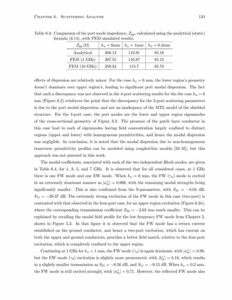
Chapter 6. Scattering Analysis 134
Table 6.3: Comparison of the port mode impedance, Zpp, calculated using the analytical (static)formula (6.14), with FEM simulated results.
Zpp (Ω) hu = 6mm hu = 1mm hu = 0.2mm
Analytical 308.13 116.91 85.16
FEM (1 GHz) 307.55 116.87 85.15
FEM (10 GHz) 259.24 115.7 85.78
effects of dispersion are relatively minor. For the case hu = 6 mm, the lower region’s geometry
doesn’t dominate over upper region’s, leading to significant port modal dispersion. The fact
that such a discrepancy was not observed in the 4-port scattering results for the the case hu = 6
mm (Figure 6.2) reinforces the point that the discrepancy for the 2-port scattering parameters
is due to the port modal dispersion, and not an inadequacy of the MTL model of the shielded
structure. For the 4-port case, the port modes are the lower and upper region eigenmodes
of the cross-sectional geometry of Figure 3.3. The presence of the patch layer conductor in
this case lead to each of eigenmodes having field concentration largely confined to distinct
regions (upper and lower) with homogeneous permittivities, and hence the modal dispersion
was negligible. In conclusion, it is noted that the modal dispersion due to non-homogeneous
transverse permittivity profiles can be modeled using coupled-line models [33–35], but this
approach was not pursued in this work.
The modal coefficients, associated with each of the two independent Bloch modes, are given
in Table 6.4, for 1, 3, 5, and 7 GHz. It is observed that for all considered cases, at 1 GHz
there is one FW mode and one EW mode. When hu = 6 mm, the FW (γa) mode is excited
in an extremely dominant manner as |a+m| = 0.998, with the remaining modal strengths being
significantly smaller. This is also confirmed from the S-parameters, with S21 = −0.04 dB,
S11 = −20.37 dB. The extremely strong excitation of the FW mode in this case (two-port) is
contrasted with that observed in the four-port case, for an upper region excitation (Figure 6.2e),
where the corresponding transmission coefficient S42 = −2.63 was much smaller. This can be
explained by recalling the modal field profile for the low frequency FW mode from Chapter 5,
shown in Figure 5.3. In that figure it is observed that the FW mode has a return current
established on the ground conductor, and hence a two-port excitation, which has current on
both the upper and ground conductors, provides a better field match, relative to the four-port
excitation, which is completely confined to the upper region.
Continuing at 1 GHz for hu = 1 mm, the FW mode (γa) is again dominant, with |a+m| = 0.96,
but the EW mode (γb) excitation is slightly more pronounced, with |b+m| = 0.18, which results
in a slightly smaller transmission as S21 = −0.56 dB, and S11 = −9.15 dB. When hu = 0.2 mm,
the FW mode is still excited strongly, with |a+m| = 0.71. However, the reflected FW mode also
Chapter 6. Scattering Analysis 135
has a significant excitation strength as |a−m| = 0.38, and additionally the decaying EW mode,
with |b+m| = 0.59, is also excited strongly. These effects combine in such a manner that the
transmission coefficient, S21 = −5.07 dB, is less than the reflection coefficient, S11 = −1.62 dB,
indicating that even though the dispersion corresponds to a FW pass-band, the FW mode is
not well matched to the port impedance.
At f = 3 GHz, the results are qualitatively similar for the structure with hu = 6 mm, with
a dominant FW mode excitation and a well matched transmission. However for both hu = 1
and 0.2 mm, the modes are complex with (γad)(hu=1mm) = 1.35 + 1.73 j, (γbd)(hu=1mm) =
1.35−1.73 j, and (γad)(hu=0.2mm) = 2.46+0.65 j, (γbd)(hu=0.2mm) = 2.46−0.65 j. It is observed
that the modes corresponding to exponential decay are excited with equal strengths, |a+m| = 0.71
and |b+m| = 0.71, while those with exponential increase are negligibly excited, for both hu = 1
mm and hu = 0.2 mm. This results in a stop-band for the structure with S11 ≈ 0 for both
hu = 1 and 0.2 mm. The larger αd value for hu = 0.2 mm shows up in the fact that the
transmission coefficient, S21 is smaller in that case, which is seen in comparing Figures 6.8d
and 6.8f.
The equal strength excitation of the complex modes corresponding to exponential decay,
for such a two-port geometry, is not a completely general phenomenon. For example, it does
not occur if the product (αd)× (N) is small. An approximate solution to the system, (6.19), in
the case that (αd)× (N) 1 may be shown to yield |a+m| = |b+m| = 0.71, with |a−m| = |b−m| = 0.
However, in practice, due to the exponential dependence of the system on (αd) × (N), the
approximate solution |a+m| = |b+m| = 0.71 holds even for the cases considered where the products,
(αd)(hu=1mm) × (N) = 6.75 and (αd)(hu=0.2mm) × (N) = 12.3, are not significantly larger than
unity. The resonant-like dips observed in S21 are a signature for the existence of complex
modes, and are a more pronounced version of what was observed in the four-port case (compare
Figure 6.8 with Figures 6.2 to 6.4 within the complex mode band). Using the approximation
|a+m|, |b+m| |a−m|, |b−m|, the voltage, V1(Nd), which is proportional to V −
M2 , is given by:
V1(Nd) = a+mV
a1 e
(−α−j β)dN + b+mVb1 e
(−α+j β)dN (6.23)
In general a+m and b+m are related through a complex phase, such that a+
m
b+m= e−2 jφ4 , with a
similar relation holding for the modal voltage coefficients, V a1V b1
= e2jφ1 . Using these relations,
(6.23) becomes:
V1(Nd) = b+mVb1 e
(−αdN−jφ4+jφ1) ×(ej(φ1−φ4−βdN) + e−j(φ1−φ4−βdN)
)= b+mV
b1 e
(−αdN−jφ4+jφ1)[2 cos(φ1 − φ4 − βdN)
] (6.24)
For a given cascade N is fixed, but βd varies as the frequency is swept through the complex mode
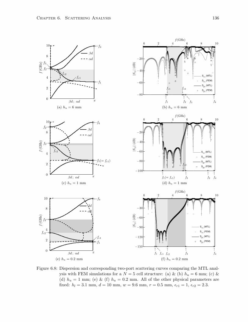
Chapter 6. Scattering Analysis 136
(a) hu = 6 mm (b) hu = 6 mm
(c) hu = 1 mm (d) hu = 1 mm
(e) hu = 0.2 mm (f) hu = 0.2 mm
Figure 6.8: Dispersion and corresponding two-port scattering curves comparing the MTL anal-ysis with FEM simulations for a N = 5 cell structure: (a) & (b) hu = 6 mm; (c) &(d) hu = 1 mm; (e) & (f) hu = 0.2 mm. All of the other physical parameters arefixed: hl = 3.1 mm, d = 10 mm, w = 9.6 mm, r = 0.5 mm, εr1 = 1, εr2 = 2.3.

Chapter 6. Scattering Analysis 137
band. The transmission zeroes correspond to frequencies for which (φ1−φ4−βdN) = π2 (2n+1).
For small values of hu, βd is swept from the value π to 0, over a narrower band, corresponding to
more closely spaced transmission zeros on the S-parameter curves, as is observed in Figure 6.8.
It is emphasized again, that these resonant dips occur only in the complex mode band, and are
a unique signature of its existence.
For f = 5 GHz, the structure with hu = 6 mm has entered a complex mode band, while the
hu = 1 mm structure remains within a complex mode band, with results which are qualitatively
identical to those discussed above. However for hu = 0.2 mm the structure has entered a band
defined by pairs of independent evanescent modes, with γad = 1.13 + j 0 and γbd = 3.16 + j 0.
Only the mode, γad, with the smaller decay constant, αad = 1.13 is significantly excited, with
|a+m| = 0.998, which also occurred in the four-port case. The resulting smooth shape of S21
curve reflects that typically encountered when standard evanescent modes are excited, with the
resonant dips observed in the complex mode case eliminated. It is also observed that there is
a significantly more pronounced variation of S21 in the EW mode band in comparison to the
complex mode band. From a qualitative viewpoint, for both the two-port and the four-port
scattering analysis, the transmission across a cascade of unit cells is small when exciting the
structure within the frequency range spanned by the complex mode band and the evanescent
mode band. This confirms that both the complex band and the evanescent bands act as stop-
bands for the structure.
6.5 Summary
In this chapter the scattering characteristics of a cascade of unit cells of the shielded struc-
ture were examined. The scattering analysis extends the applicability of the MTL model by
accounting for the more realistic situation were a finite number of unit cells are excited.
The scattering analysis is connected with the previously obtained dispersion analysis in
multiple ways. It was shown that a general excitation of the structure corresponds to a linear
combination of all possible Bloch modes. This confirmed that the dispersion analysis, which
describes the propagation properties of a single unit cell, may be extended to model the scat-
tering effects of a cascade of unit cells. The scattering analysis also provides a confirmation of
the nature of the modes which exist in the stop-band. Although the MTL model accounted
for both pass-bands and stop-bands the FEM eigenmode simulations did not provide the prop-
agation constants within the stop-bands. Driven FEM simulations, on the other hand, which
corresponded to various scattering situations, were shown to confirm the modal nature of the
stop-band as predicted by the MTL model: both complex modes and pairs of standard evanes-
cent modes were shown to be supported by the structure. The existence of complex modes and
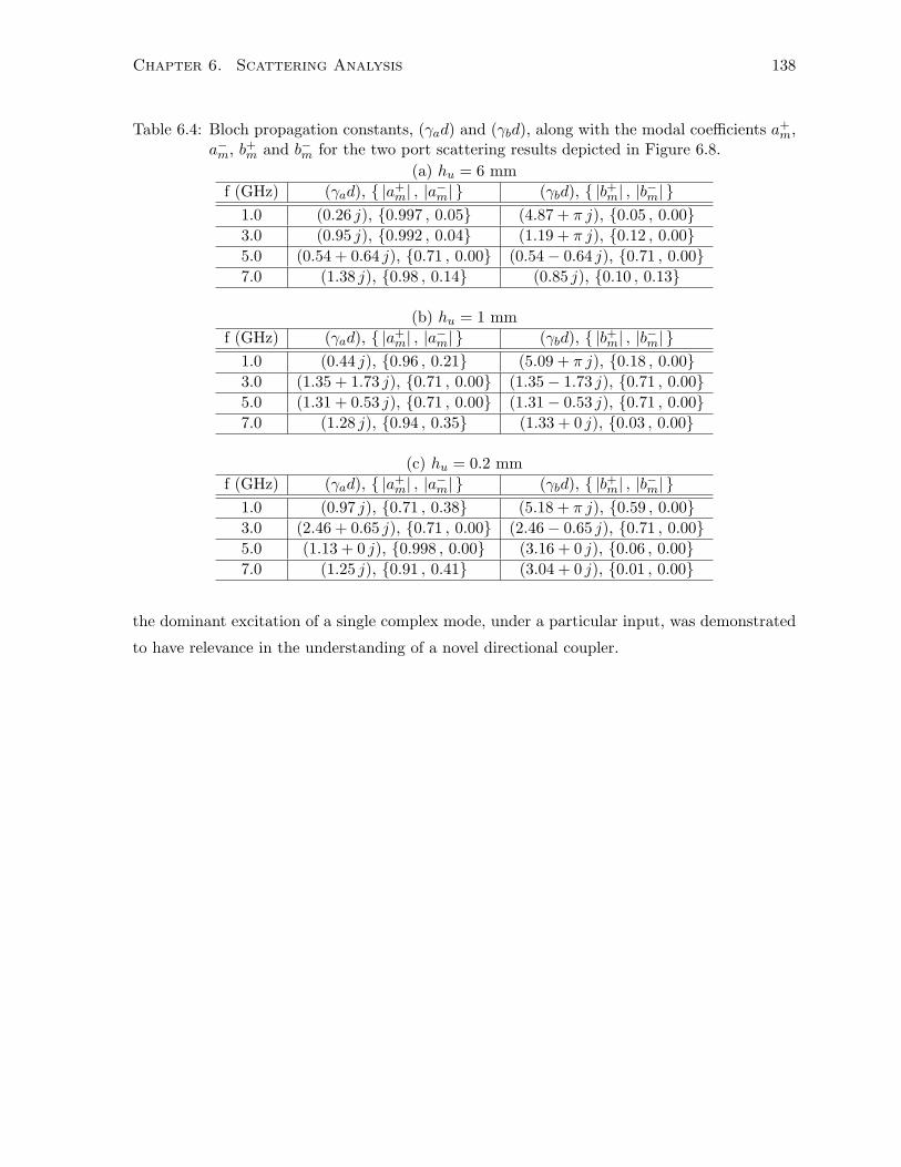
Chapter 6. Scattering Analysis 138
Table 6.4: Bloch propagation constants, (γad) and (γbd), along with the modal coefficients a+m,
a−m, b+m and b−m for the two port scattering results depicted in Figure 6.8.(a) hu = 6 mm
f (GHz) (γad), |a+m| , |a−m| (γbd), |b+m| , |b−m|
1.0 (0.26 j), 0.997 , 0.05 (4.87 + π j), 0.05 , 0.003.0 (0.95 j), 0.992 , 0.04 (1.19 + π j), 0.12 , 0.005.0 (0.54 + 0.64 j), 0.71 , 0.00 (0.54− 0.64 j), 0.71 , 0.007.0 (1.38 j), 0.98 , 0.14 (0.85 j), 0.10 , 0.13
(b) hu = 1 mmf (GHz) (γad), |a+
m| , |a−m| (γbd), |b+m| , |b−m| 1.0 (0.44 j), 0.96 , 0.21 (5.09 + π j), 0.18 , 0.003.0 (1.35 + 1.73 j), 0.71 , 0.00 (1.35− 1.73 j), 0.71 , 0.005.0 (1.31 + 0.53 j), 0.71 , 0.00 (1.31− 0.53 j), 0.71 , 0.007.0 (1.28 j), 0.94 , 0.35 (1.33 + 0 j), 0.03 , 0.00
(c) hu = 0.2 mmf (GHz) (γad), |a+
m| , |a−m| (γbd), |b+m| , |b−m| 1.0 (0.97 j), 0.71 , 0.38 (5.18 + π j), 0.59 , 0.003.0 (2.46 + 0.65 j), 0.71 , 0.00 (2.46− 0.65 j), 0.71 , 0.005.0 (1.13 + 0 j), 0.998 , 0.00 (3.16 + 0 j), 0.06 , 0.007.0 (1.25 j), 0.91 , 0.41 (3.04 + 0 j), 0.01 , 0.00
the dominant excitation of a single complex mode, under a particular input, was demonstrated
to have relevance in the understanding of a novel directional coupler.
Chapter 7
Shielded structure based slot
antenna
7.1 Introduction
Printed slot antennas have been extensively studied due to their low profile, low cost, light
weight and ease of fabrication [42]. However, a single slot antenna printed on a thin dielectric
substrate is essentially a bi-directional radiator, with the back radiation being undesirable.
There have been several methods which successfully demonstrated reduced back radiation.
One method is to print the slots on electrically thick substrates or at the back of dielectric
lenses. For an infinitesimal slot printed on a quarter dielectric wavelength thick substrate, the
front-to-back power density ratio at broadside is equal to the substrate relative permittivity εr,
and for a slot antenna printed on a hemispheric dielectric lens the ratio is ε3/2r [43]. The main
drawback of these techniques is the severe loss due to surface wave excitation in the former case,
and the lack of a low-profile character in the latter. For an array of slot radiators the above
drawbacks may be alleviated by using phase cancellation techniques [44–46], which utilize the
proper spacing of array elements to achieve destructive interference of surface wave modes.
A common technique employed to restore the back radiation is backing the slot with a
metallic cavity (box) [47]. While a uni-directional pattern may be achieved, a drawback of this
method is the additional manufacturing difficulty in machining the cavity, especially for array
designs. In addition, spurious resonances may be produced, limiting the resulting bandwidth.
Another method commonly employed to reduce the back-radiation is the addition of a back-
ing metallic reflector in order to redirect the back radiation forward [48]. The main drawback in
this case is that the geometry of the antenna now is transformed into a parallel-plate environ-
ment and hence the excitation of the parallel-plate TEM mode degrades the radiation efficiency
as well as the antenna patterns. In addition, the reflector must be placed a quarter-wavelength
139
Chapter 7. Shielded structure based slot antenna 140
away from the slot ground-plane for proper operation. Hence the resulting structure is not of
a low-profile nature at lower RF frequencies.
In order to mitigate the effects of the excited TEM mode in conductor-backed slot antennas
various types of periodically loaded structures, also referred to as electromagnetic band-gap
(EBG) structures have been utilized. Within the stop-bands of these structures electromag-
netic wave propagation is prohibited [49], and it can be expected that if a slot antenna is
designed to resonate in the stop-band of a properly designed EBG structure, with a complete
2D (omni-directional) band-gap, the parallel-plate mode becomes evanescent. Hence, in such
an arrangement the radiation front-to-back ratio and the patterns should be improved com-
pared to the case of a simple conductor-backed slot. Such an approach has been utilized in
[50, 51]. In [50], a square lattice of holes was drilled in a substrate in order to create an EBG
structure. In this case though, the periodic pattern of the substrate does not greatly perturb
the underlying parallel-plate environment, and thus the position of the stop-band is essentially
determined by the lattice spacing, hence compromising compactness at low microwave and RF
frequencies. This becomes evident by noting that the unit cell periodicity in [50] is 1.2 cm
when the band-gap lies between 7.5 and 10 GHz. In addition, the achievable bandwidth for
the stop-band is smaller than that of the structure proposed in this chapter. In [51] a two-
dimensional EBG surface was constructed by etching a periodic metallic pattern and utilized to
back a microstrip-fed slot antenna. The resulting perforated ground plane is prone to leakage
through radiation, and hence an additional ground plane must be added behind the perforated
plane thus adding to fabrication complexity and possibly limiting the useful bandwidth.
The shielded Sievenpiper geometry has been demonstrated to be a suitable metallic EBG
structure which is not prone to radiation leakage, as it has a solid ground plane, and can
also maintain a compact geometry when implemented at frequencies in the range of 3 to 5
GHz. The configuration to be studied in this chapter consists of a coplanar waveguide (CPW)
fed ring-slot antenna, which is chosen to maintain compactness, and is printed on the upper
shielding conductor of the shielded Sievenpiper structure. By operating within the stop-band,
it is expected that most of the energy radiated by the slot into the shielded structure will be
redirected back into the region above the shielding plane, resulting in a uni-directional antenna.
This EBG based antenna may be designed to maintain a low profile, with an overall thickness
mush less than a quarter wavelength ( λ4 ), which is another advantage when compared to
the standard conductor backed antenna. In the next section the design of the underlying
shielded structure will be detailed, followed by the antenna design, with experimental results
and conclusions following.
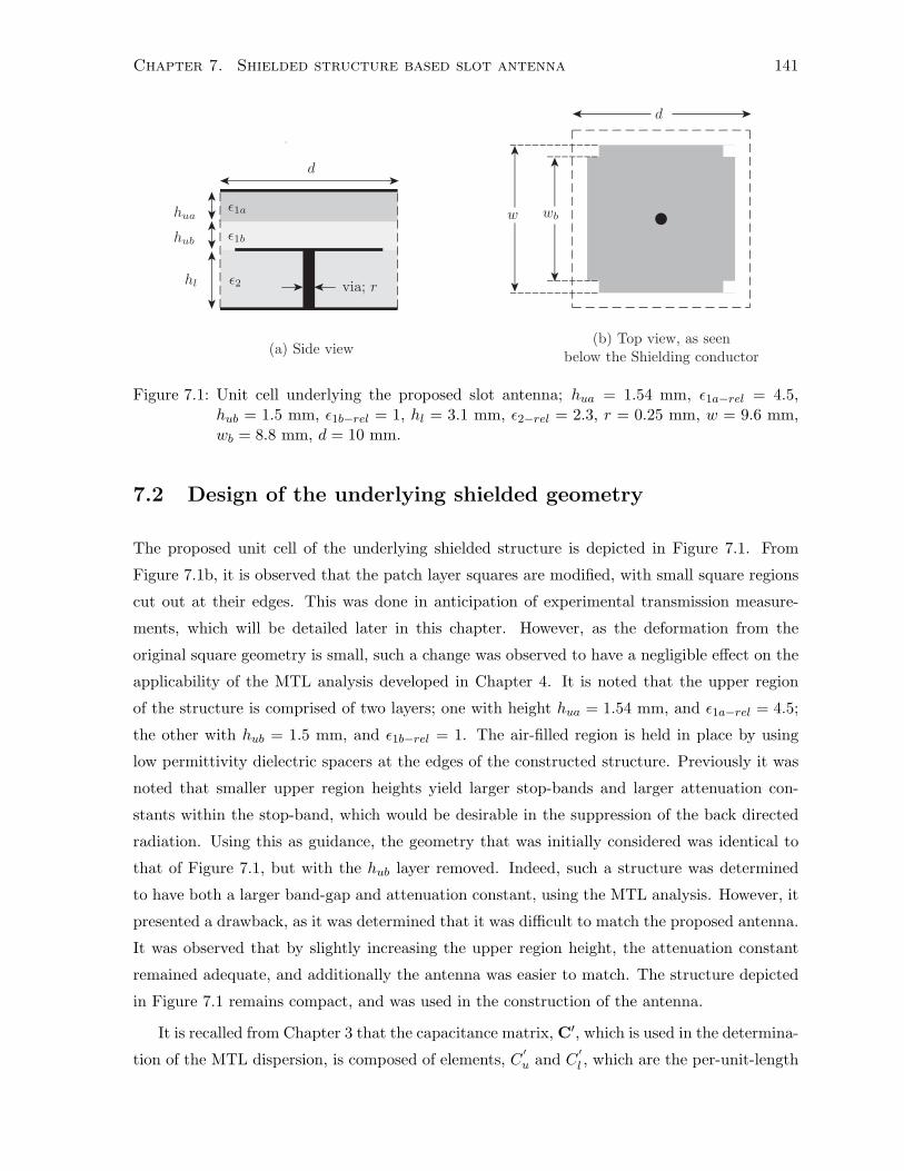
Chapter 7. Shielded structure based slot antenna 141
hua
hub
hl
ǫ1a
ǫ1b
ǫ2
w wb
d
d
via; r
(a) Side view(b) Top view, as seen
below the Shielding conductor
Figure 7.1: Unit cell underlying the proposed slot antenna; hua = 1.54 mm, ε1a−rel = 4.5,hub = 1.5 mm, ε1b−rel = 1, hl = 3.1 mm, ε2−rel = 2.3, r = 0.25 mm, w = 9.6 mm,wb = 8.8 mm, d = 10 mm.
7.2 Design of the underlying shielded geometry
The proposed unit cell of the underlying shielded structure is depicted in Figure 7.1. From
Figure 7.1b, it is observed that the patch layer squares are modified, with small square regions
cut out at their edges. This was done in anticipation of experimental transmission measure-
ments, which will be detailed later in this chapter. However, as the deformation from the
original square geometry is small, such a change was observed to have a negligible effect on the
applicability of the MTL analysis developed in Chapter 4. It is noted that the upper region
of the structure is comprised of two layers; one with height hua = 1.54 mm, and ε1a−rel = 4.5;
the other with hub = 1.5 mm, and ε1b−rel = 1. The air-filled region is held in place by using
low permittivity dielectric spacers at the edges of the constructed structure. Previously it was
noted that smaller upper region heights yield larger stop-bands and larger attenuation con-
stants within the stop-band, which would be desirable in the suppression of the back directed
radiation. Using this as guidance, the geometry that was initially considered was identical to
that of Figure 7.1, but with the hub layer removed. Indeed, such a structure was determined
to have both a larger band-gap and attenuation constant, using the MTL analysis. However, it
presented a drawback, as it was determined that it was difficult to match the proposed antenna.
It was observed that by slightly increasing the upper region height, the attenuation constant
remained adequate, and additionally the antenna was easier to match. The structure depicted
in Figure 7.1 remains compact, and was used in the construction of the antenna.
It is recalled from Chapter 3 that the capacitance matrix, C′, which is used in the determina-
tion of the MTL dispersion, is composed of elements, C′u and C
′l , which are the per-unit-length

Chapter 7. Shielded structure based slot antenna 142
(scalar) capacitances of parallel-plate geometries consisting of the upper and lower regions
alone. However, for all previously considered geometries (Figure 3.3), the upper region (height
hu) consisted of a uniform dielectric with permittivity ε1, with the lower region (height hl)
also a uniform medium with dielectric constant, ε2. For the structure proposed in Figure 7.1
the upper region is composed of two uniform layers, and hence the expression for C′u needs to
be changed appropriately. The modified (non-uniform) upper region capacitance, C′u(n.u.) is
formed from the series combination of two per-unit-length capacitances, C′u(hua) and C
′u(hub),
C′u(hua) =
ε1ad
hua(7.1)
C′u(hub) =
ε1bd
hub(7.2)
with C′u(n.u.) given by
1C ′u(n.u.)
=1
C ′u(hua)+
1C ′u(hub)
(7.3)
With this modification the previously developed MTL analysis may be applied to the present
structure. The loading components, calculated to be L = 1.15 nH, and C = 0.23 pF are deter-
mined using scattering analysis as shown in Chapter 3. The MTL theory dispersion curves are
compared with FEM generated results in Figure 7.2. It is observed that there is excellent cor-
respondence between the two sets of curves, with a band-gap for on-axis propagation extending
from approximately 2.59 to 5.09 GHz.
In order to verify that an omni-directional stop-band is achieved, a full two-dimensional
Brillouin diagram has been generated using FEM simulations, with the results depicted in
Figure 7.3. The dispersion diagram is shown for the irreducible Brillouin zone; the portion of
the curve from Γ to X has 0 ≤ βxd ≤ π, with βyd = 0 fixed; from X to M , βxd = π is fixed
with 0 ≤ βyd ≤ π; finally for M to Γ, both βxd = βyd vary from π to 0. It is observed that a
complete omnidirectional band-gap exists from approximately 2.5 to 5.0 GHz.
An experimental determination of the stop-band of the designed structure was performed
next, with a schematic of the test method shown in Figure 7.4. The constructed shielded
structure was ten by ten unit cells (Figure 7.4a). Additionally, a parallel plate geometry, with
the mushroom surface replaced by a solid ground plane was also considered (Figure 7.4b). Two
holes are drilled into the top conductor so that co-axial probes may be placed about 8 cm
apart, forming two (coaxial) ports. The outer conductor of the co-axial probe is connected to
the shielding plate and the inner conductor goes through the structure, (and through the gaps
cut out of the patch corners) and is connected to the solid ground plane. From this arrangement
the transmission parameter S21 was experimentally measured, with the resulting data shown
in Figure 7.4c for the Γ−X direction, and Figure 7.4d for the M − Γ direction.

Chapter 7. Shielded structure based slot antenna 143
Figure 7.2: Comparison of MTL theory with FEM generated dispersion curves for on-axis prop-agation for the geometry of Figure 7.1.
Figure 7.3: FEM simulated Brillouin diagram for the shielded structure of Figure 7.1 showinga complete omni-directional band-gap between approximately 2.5 and 5 GHz.

Chapter 7. Shielded structure based slot antenna 144
Port 1 Port 2
8 cm
co-axial probes
(a) Shielded geometry of Figure 7.1.
Port 1 Port 2
8 cm
co-axial probes
(b) Parallel plate geometry.
2 3 4 5 6−100
−80
−60
−40
−20
0
Frequency (GHz)
S21
(d
B)
S21
: EBG
S21
: PP
(c) (d)
Figure 7.4: Coaxial excitation of: (a) the shielded structure, and (b) a parallel-plate geometry(with the mushroom structure replaced with a solid ground plane), for the purposeof measuring the transmission, S21; Measured S21 for the shielded structure, andfor the flat conductor backed parallel-plate structure for: (c) the Γ −X direction;(d) the Γ−M direction.
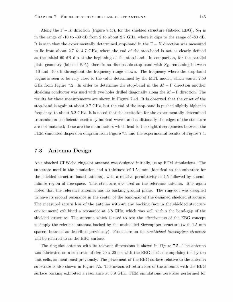
Chapter 7. Shielded structure based slot antenna 145
Along the Γ − X direction (Figure 7.4c), for the shielded structure (labeled EBG), S21 is
in the range of -10 to -30 dB from 2 to about 2.7 GHz, where it dips to the range of -80 dB.
It is seen that the experimentally determined stop-band in the Γ−X direction was measured
to lie from about 2.7 to 4.7 GHz, where the end of the stop-band is not as clearly defined
as the initial 60 dB dip at the beginning of the stop-band. In comparison, for the parallel
plate geometry (labeled P.P.), there is no discernable stop-band with S21 remaining between
-10 and -40 dB throughout the frequency range shown. The frequency where the stop-band
begins is seen to be very close to the value determined by the MTL model, which was at 2.59
GHz from Figure 7.2. In order to determine the stop-band in the M − Γ direction another
shielding conductor was used with two holes drilled diagonally along the M −Γ direction. The
results for these measurements are shown in Figure 7.4d. It is observed that the onset of the
stop-band is again at about 2.7 GHz, but the end of the stop-band is pushed slightly higher in
frequency, to about 5.2 GHz. It is noted that the excitation for the experimentally determined
transmission coefficients excites cylindrical waves, and additionally the edges of the structure
are not matched; these are the main factors which lead to the slight discrepancies between the
FEM simulated dispersion diagram from Figure 7.3 and the experimental results of Figure 7.4.
7.3 Antenna Design
An unbacked CPW-fed ring-slot antenna was designed initially, using FEM simulations. The
substrate used in the simulation had a thickness of 1.54 mm (identical to the substrate for
the shielded structure-based antenna), with a relative permittivity of 4.5 followed by a semi-
infinite region of free-space. This structure was used as the reference antenna. It is again
noted that the reference antenna has no backing ground plane. The ring-slot was designed
to have its second resonance in the center of the band-gap of the designed shielded structure.
The measured return loss of the antenna without any backing (not in the shielded structure
environment) exhibited a resonance at 3.8 GHz, which was well within the band-gap of the
shielded structure. The antenna which is used to test the effectiveness of the EBG concept
is simply the reference antenna backed by the unshielded Sievenpiper structure (with 1.5 mm
spacers between as described previously). From here on the unshielded Sievenpiper structure
will be referred to as the EBG surface.
The ring-slot antenna with its relevant dimensions is shown in Figure 7.5. The antenna
was fabricated on a substrate of size 20 x 20 cm with the EBG surface comprising ten by ten
unit cells, as mentioned previously. The placement of the EBG surface relative to the antenna
substrate is also shown in Figure 7.5. The measured return loss of the antenna with the EBG
surface backing exhibited a resonance at 3.9 GHz. FEM simulations were also performed for
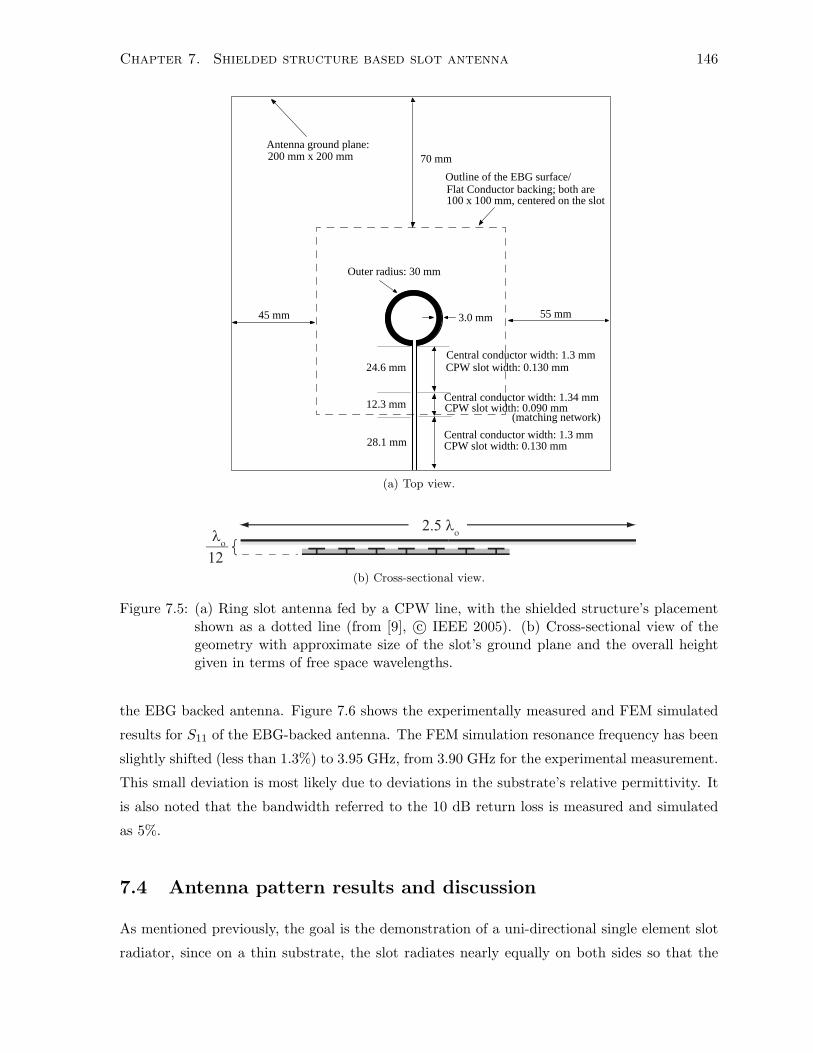
Chapter 7. Shielded structure based slot antenna 146
3.0 mm45 mm 55 mm
70 mm
Central conductor width: 1.3 mmCPW slot width: 0.130 mm
Central conductor width: 1.34 mmCPW slot width: 0.090 mm
Central conductor width: 1.3 mmCPW slot width: 0.130 mm
Outer radius: 30 mm
Antenna ground plane:200 mm x 200 mm
Outline of the EBG surface/Flat Conductor backing; both are100 x 100 mm, centered on the slot
(matching network)
24.6 mm
12.3 mm
28.1 mm
(a) Top view.
λο
12
2.5 λο
(b) Cross-sectional view.
Figure 7.5: (a) Ring slot antenna fed by a CPW line, with the shielded structure’s placementshown as a dotted line (from [9], c© IEEE 2005). (b) Cross-sectional view of thegeometry with approximate size of the slot’s ground plane and the overall heightgiven in terms of free space wavelengths.
the EBG backed antenna. Figure 7.6 shows the experimentally measured and FEM simulated
results for S11 of the EBG-backed antenna. The FEM simulation resonance frequency has been
slightly shifted (less than 1.3%) to 3.95 GHz, from 3.90 GHz for the experimental measurement.
This small deviation is most likely due to deviations in the substrate’s relative permittivity. It
is also noted that the bandwidth referred to the 10 dB return loss is measured and simulated
as 5%.
7.4 Antenna pattern results and discussion
As mentioned previously, the goal is the demonstration of a uni-directional single element slot
radiator, since on a thin substrate, the slot radiates nearly equally on both sides so that the

Chapter 7. Shielded structure based slot antenna 147
3.7 3.8 3.9 4.0
−13
−11
−9
−7
−5
Frequency (GHz)
S11
(d
B)
MeasuredFEM
Figure 7.6: S11 of the shielded structure-based slot antenna (from [9], c© IEEE 2005).
front-to-back ratio is close to 0 dB. The normalized patterns of the reference ring-slot antenna
(the antenna of Figure 7.5 without the backing EBG surface) are shown in Figure 7.7, where it
is clearly seen that the radiated power is bi-directional. It is observed that the FEM generated
patterns match the measured patterns very well. The lack of a null over the horizontal (ground)
plane in the H-plane is attributed to the finite size of the antenna ground plane. Furthermore,
the finite size of the ground plane manifests itself in the E-plane ripples, which are due to edge
diffraction.
A finite metal plate of size 10 x 10 cm was used as a plane reflector, and it was placed a
quarter wavelength (20 mm) from the ring-slot’s ground plane so that the reflected fields would
add in phase to the forward directed fields. The corresponding normalized patterns are shown
in Figure 7.8. It is seen that the front-to-back ratio is improved to approximately 8 dB at
broadside. In addition, distinct undulations appear in the back-radiated E-plane pattern. This
relatively low front-to-back ratio is most likely due to radiation of the trapped parallel-plate
mode which diffracts from the edges of the plates. Suppression of this mode must be achieved
in order to increase the front-to-back ratio and smooth out the patterns.
The unwanted effect of this parasitic radiation should be eliminated if the trapped parallel-
plate mode is forbidden from propagating in the underlying geometry, which is achieved with
the shielded structure. The corresponding patterns when backing the ring-slot antenna with
the EBG surface are depicted in Figure 7.9. It is observed that the experimentally measured
and FEM simulated patterns match very well again. As shown, the front-to-back ratio is
approximately 20 dB at broadside. The relative gain improvement at broadside in both the E
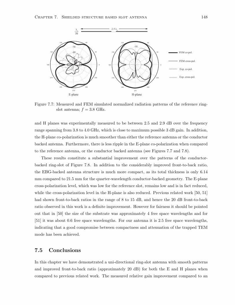
Chapter 7. Shielded structure based slot antenna 148
2.5 λο
E-plane H-plane
FEM co-pol.
FEM cross-pol.
Exp. co-pol.
Exp. cross-pol.
λο
50
30
210
60
240
270
120
300
150
330
180 0
-10
-20 30
210
60
240
270
120
300
150
330
180 0
-10
--20
Figure 7.7: Measured and FEM simulated normalized radiation patterns of the reference ring-slot antenna; f = 3.8 GHz.
and H planes was experimentally measured to be between 2.5 and 2.9 dB over the frequency
range spanning from 3.8 to 4.0 GHz, which is close to maximum possible 3 dB gain. In addition,
the H-plane co-polarization is much smoother than either the reference antenna or the conductor
backed antenna. Furthermore, there is less ripple in the E-plane co-polarization when compared
to the reference antenna, or the conductor backed antenna (see Figures 7.7 and 7.8).
These results constitute a substantial improvement over the patterns of the conductor-
backed ring-slot of Figure 7.8. In addition to the considerably improved front-to-back ratio,
the EBG-backed antenna structure is much more compact, as its total thickness is only 6.14
mm compared to 21.5 mm for the quarter-wavelength conductor-backed geometry. The E-plane
cross-polarization level, which was low for the reference slot, remains low and is in fact reduced,
while the cross-polarization level in the H-plane is also reduced. Previous related work [50, 51]
had shown front-to-back ratios in the range of 8 to 15 dB, and hence the 20 dB front-to-back
ratio observed in this work is a definite improvement. However for fairness it should be pointed
out that in [50] the size of the substrate was approximately 4 free space wavelengths and for
[51] it was about 0.6 free space wavelengths. For our antenna it is 2.5 free space wavelengths,
indicating that a good compromise between compactness and attenuation of the trapped TEM
mode has been achieved.
7.5 Conclusions
In this chapter we have demonstrated a uni-directional ring-slot antenna with smooth patterns
and improved front-to-back ratio (approximately 20 dB) for both the E and H planes when
compared to previous related work. The measured relative gain improvement compared to an

Chapter 7. Shielded structure based slot antenna 149
30
210
60
240
270
120
300
150
330
180 0
30
210
60
240
270
120
300
150
330
180 0
E-plane H-plane
FEM co-pol.
FEM cross-pol.
Exp. co-pol.
Exp. cross-pol.
λο
4
2.5 λο
Figure 7.8: Measured and FEM simulated normalized radiation patterns of the reference ring-slot antenna backed with a conductor at one quarter wavelength; f = 3.7 GHz.
30
210
60
240
270
120
300
150
330
180 0
-10
-20 30
210
60
240
270
120
300
150
330
180 0
-10
-20
E-plane H-plane
FEM co-pol.
FEM cross-pol.
Exp. co-pol.
Exp. cross-pol.
λο
12
2.5 λο
Figure 7.9: Measured and FEM simulated normalized radiation patterns of the reference ring-slot antenna backed with the EBG; f = 3.9 GHz.

Chapter 7. Shielded structure based slot antenna 150
unbacked ring-slot antenna was between 2.5 and 2.9 dB over the frequency span of 3.8 to 4.0
GHz. This was achieved by using the shielded Sievenpiper structure as an underlying EBG
structure which supports an omni-directional stop-band. Full-wave simulations were shown,
which matched well the experimental data for both the radiation patterns and the shielded
structure’s stop-band. Compared to the standard quarter wavelength conductor-backed config-
uration, the EBG-backed ring-slot offers an improved front-to-back ratio (from approximately 8
dB to 20 dB) and compactness of the antenna both laterally and in terms of thickness (75% size
reduction). It has thus been demonstrated that the use of a properly designed EBG structure
can lead to a compact unidirectional slot antenna at RF frequencies.
Chapter 8
Conclusions
8.1 Summary of Contributions
In this thesis, periodic transmission line (TL) analysis, which is applicable for loaded 2-conductor
geometries, was extended and generalized to the case of loaded, coupled (n+ 1)-conductor ge-
ometries, using multiconductor transmission line (MTL) theory. Standard periodic TL analysis
can account for only a single mode of propagation, and hence is inadequate for structures which
support bands with multiple coupled modes. Using MTL theory, a concise analytical description
and intuitive understanding of the wave propagation properties of such multi-mode structures
was obtained.
In particular, the shielded Sievenpiper structure was studied in depth. The shielded Sieven-
piper structure and several other topologically related structures, both shielded and unshielded,
have been shown to be useful in a wide variety of applications, including noise suppression in
digital circuits, the creation of uni-directional slot antennas, the analysis of artificial media, in-
cluding slow-wave structures and negative refractive index media, and in the understanding and
analysis of novel compact coupled-line couplers. Although the developed theory is applicable
for all of the above mentioned applications, the specific geometry of the shielded Sievenpiper
structure admits a particularly simple description in terms of the two distinct regions of the
structure: the upper region and the lower region. The underlying electrical parameters which
describe this multiconductor system are related to simple parallel-plate geometries, which allows
for significant simplification of the analytical model, while still retaining accuracy. The above
factors made the shielded Sievenpiper structure an ideal candidate as a canonical example of
the developed theory.
Multiconductor transmission line theory was used to determine the dispersion behaviour
of the shielded Sievenpiper structure under changing geometric parameters. When the height
of the upper region was sufficiently large, the structure was observed to support a dual mode
151

Chapter 8. Conclusions 152
initial pass-band, with a stop-band formed from the contra-directional coupling of a forward
wave (FW) mode and a backward wave (BW) mode. The nature of the modes in the stop-
band were not typical: they were described by pairs given by complex conjugate propagation
constants, which are referred to as complex modes. The properties of complex modes were
reviewed. As the upper region height was decreased, the dispersion of the FW mode became
flatter, indicating a slow wave effect, and the bandwidth of the BW mode decreased. For small
enough upper region heights, the qualitative nature of the dispersion curves changed, and the
BW mode was eliminated, resulting in an initial band which contained only a single FW mode.
The theory also revealed that for such cases the stop-band consisted of a union of regions defined
by complex modes, in addition to regions described by standard evanescent modes.
Critical points, which characterize band transitions, were analytically determined, leading to
a deeper understanding of the parameters which controlled the shape of the dispersion curves.
It was shown that some of the critical points were dependent on properties of the upper or
lower regions alone, while others were dependent on combinations of both. Additionally, a
physical explanation of the transition from dual mode to single mode behaviour was obtained
by examining these critical points.
In the low frequency limit the theory revealed that the structure supported a slow FW
mode. By examining the propagation constant of this mode, along with the modal eigenvector,
an interesting physical explanation of this effect was suggested. In particular, it was shown that
the slow wave effect was due to a per-unit-length capacitance enhancement, with the per-unit-
length inductance remaining invariant. These results were related to the simple geometrical
parameters which characterize the structure.
In addition to the periodic analysis, various forms of scattering analysis were examined.
By considering a finite cascade of unit cells of the shielded structure, with different types
of excitation mechanisms, generalized scattering parameters were obtained using the MTL
analysis. The results were shown to have excellent correspondence with FEM simulations,
over a wide frequency range, including pass-bands, complex mode bands, and evanescent wave
bands. The different excitations corresponded to different applications, and these were noted.
A slot antenna utilizing the shielded Sievenpiper structure was designed and constructed.
By operating the antenna in the frequency range defined by the band-gap of the structure,
a uni-directional slot antenna was demonstrated. Measurements were made, and compared
with those of an un-backed slot antenna, and a conductor-backed slot antenna. The shielded
structure based slot antenna was more compact, and observed to have a larger broadside gain
than the conductor-backed antenna.
Having listed the specific contributions, the overarching contribution of this work will be
described now. Periodically loaded transmission line theory has long been a useful tool in

Chapter 8. Conclusions 153
the analysis of electromagnetic wave propagation problems. However it is limited in that it
can only model a single mode of propagation. The periodic multiconductor transmission line
analysis developed in this thesis provides an extension to standard periodic transmission line
theory, as it is capable of modeling multi-mode behaviour. However, it was shown that even
in cases where the dispersion of the structure is single mode, as it can be for the shielded
Sievenpiper structure, a simple TL model is not adequate. In such cases MTL analysis is still
needed to accurately account for the dispersion, especially in the stop-band, where complex
modes are supported. The analysis method developed in this thesis, in addition to providing an
extension to TL analysis which is capable of accurately capturing multi-mode behaviour, will
provide researchers with an awareness of the usefulness of the multi-modal viewpoint, even in
structures which nominally support single (propagating) mode bands.
8.2 Publications
Parts of the work presented in this thesis have appeared in the publications listed below.
Refereed Journal Papers
1. F. Elek and G.V. Eleftheriades, “Dispersion analysis of the shielded Sievenpiper structure
using multiconductor transmission-line theory,” IEEE Microwave and Wireless Compo-
nent Letters, vol. 14, no. 9, pp. 434-436, Sep. 2004.
2. F. Elek, R. Abhari and G.V. Eleftheriades, “A uni-directional ring-slot antenna achieved
by using an electromagnetic band-gap surface,” IEEE Transactions on Antennas and
Propagation, vol. 53, no. 1, pp. 181-190, Jan. 2005.
3. F. Elek and G.V. Eleftheriades, “A two-dimensional uniplanar transmission-line meta-
material with a negative index of refraction,” New Journal of Physics; Focused Issue on
Negative Refraction, vol. 7, no. 163, pp. 1-18, Aug. 2005.
4. R. Islam, F. Elek and G.V. Eleftheriades, “Coupled-line metamaterial coupler having co-
directional phase but contra-directional power flow,” Electronics Letters, vol. 40, no. 5,
pp. 315-317, Mar. 2004.
5. M. Stickel, F. Elek, J. Zhu and G. V. Eleftheriades, “Volumetric negative-refractive-index
metamaterials based upon the shunt-node transmission-line configuration,” Journal of
Applied Physics, vol. 102, p. 094903, Nov. 2007.
Refereed Conference Proceedings

Chapter 8. Conclusions 154
1. F. Elek and G.V. Eleftheriades, “Simple analytical dispersion equations for the shielded
Sievenpiper structure,” IEEE International Microwave Symposium, San Francisco, CA,
Jun. 2006, pp. 1651-1654.
2. F. Elek and G.V. Eleftheriades, “On the slow wave behaviour of the shielded mushroom
structure,” IEEE International Microwave Symposium, Atlanta, GA, Jun. 2008, pp.
1333-1336.

Appendix A
Shielded structure based antenna
compared with a cavity-backed
antenna
In Chapter 7 a shielded structure based slot antenna (also referred to as an EBG-backed an-
tenna) was demonstrated to have a superior front-to-back ratio when compared to both a
conductor-backed antenna and a reference (un-backed) slot antenna. This was confirmed with
both pattern measurements and FEM simulations. The EBG-backed antenna achieves the im-
proved front-to-back ratio by suppressing the parallel-plate mode which is supported by the
conductor-backed design. Additionally, the EBG-backed design also has a much lower profile
( λ12) when compared to the conductor-backed antenna (λ4 ).
The parallel-plate mode may also be suppressed by backing a slot antenna with a metallic
cavity, which will be investigated in this Appendix with the aid of FEM simulations. Two
different cavity-backed designs are considered: for the first one the cavity depth is λ4 , while for
the second the cavity depth is λ12 . The FEM simulated results for the cavity-backed radiation
patterns are shown in Figure A.1, along with EBG-backed design. Comparing the EBG-backed
antenna with the λ4 cavity-backed design it is observed that similar front-to-back ratios are
observed for both the E and H planes. However, the E-plane cross-polarization is significantly
larger for the cavity-backed antenna. For the low profile ( λ12) cavity-backed design the front-
to-back ratios are again comparable to the EBG-backed design; however in this case the cross-
polarization levels for both the E and H-planes are significantly higher than the EBG-backed
antenna.
The degradation of the radiation patterns may be understood by examining the S11 curves,
which are shown in Figure A.2. The EBG-backed antenna exhibits a smooth resonance centered
155

Appendix A. Shielded structure based antenna compared with a cavity-backed antenna156
at around 3.9 GHz, while the λ4 cavity-backed design shows multiple resonances within the
depicted band. These additional resonances are due to the resonant modes of the cavity and are
responsible for the pattern degradation. For the low-profile cavity-backed design, the matching
bandwidth is much narrower, which limits it usefulness. Thus a low-profile cavity-backed design
suffers from both degraded radiation patterns and also a narrow matching bandwidth.
In summary it is noted that the EBG-backed antenna has superior performance when com-
pared to both cavity backed designs, and this is achieved while maintaining a low profile.
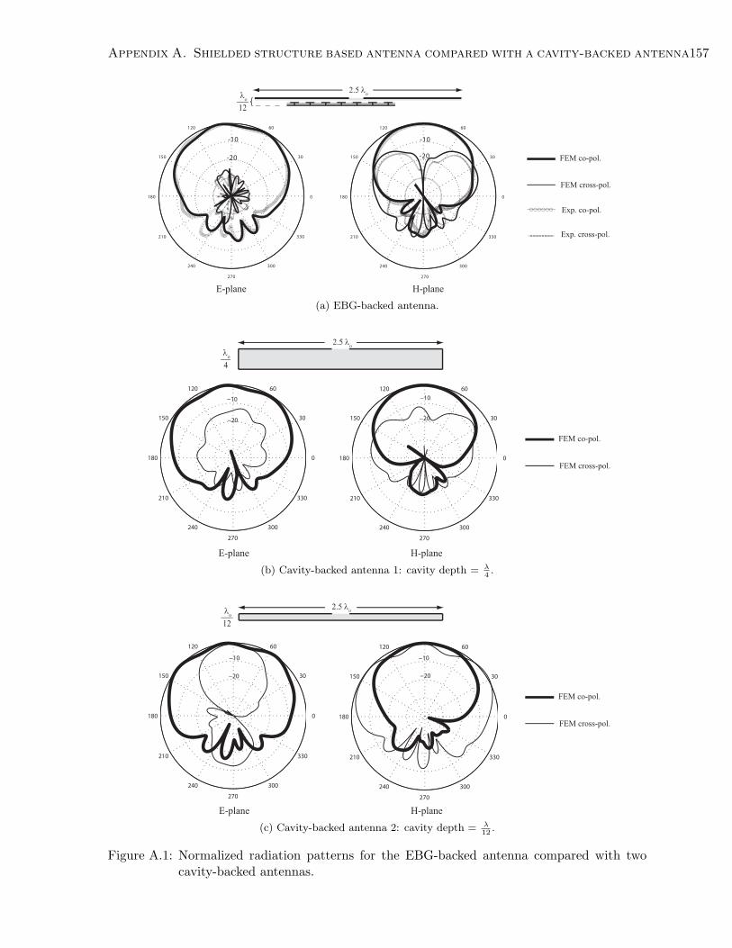
Appendix A. Shielded structure based antenna compared with a cavity-backed antenna157
30
210
60
240
270
120
300
150
330
180 0
-10
-20 30
210
60
240
270
120
300
150
330
180 0
-10
-20
E-plane H-plane
FEM co-pol.
FEM cross-pol.
Exp. co-pol.
Exp. cross-pol.
λο
12
2.5 λο
(a) EBG-backed antenna.
−20
−10
30
210
60
240
270
120
300
150
330
180 0
E-plane
−20
−10
30
210
60
240
270
120
300
150
330
180 0
H-plane
FEM co-pol.
FEM cross-pol.
λο
4
2.5 λο
(b) Cavity-backed antenna 1: cavity depth = λ4.
E-plane H-plane
FEM co-pol.
FEM cross-pol.
−20
−10
30
210
60
240
270
120
300
150
330
180 0
−20
−10
30
210
60
240
270
120
300
150
330
180 0
2.5 λολ
ο
12
(c) Cavity-backed antenna 2: cavity depth = λ12
.
Figure A.1: Normalized radiation patterns for the EBG-backed antenna compared with twocavity-backed antennas.
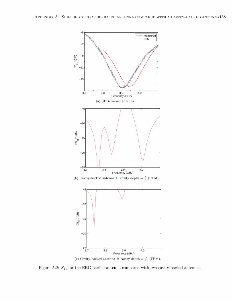
Appendix A. Shielded structure based antenna compared with a cavity-backed antenna158
3.7 3.8 3.9 4.0
−13
−11
−9
−7
−5
Frequency (GHz)
S11
(d
B)
MeasuredFEM
(a) EBG-backed antenna.
3.7 3.8 3.9 4.0−25
−20
−15
−10
−5
Frequency (GHz)
S11
(d
B)
(b) Cavity-backed antenna 1: cavity depth = λ4
(FEM).
3.7 3.8 3.9 4.0−25
−20
−15
−10
−5
Frequency (GHz)
S11
(d
B)
(c) Cavity-backed antenna 2: cavity depth = λ12
(FEM).
Figure A.2: S11 for the EBG-backed antenna compared with two cavity-backed antennas.

Bibliography
[1] L. Brillouin, “Wave guides for slow waves,” J. Appl. Phys, vol. 19, pp. 1023–1041, Nov.
1948.
[2] L. Stark, “Electromagnetic waves in periodic structures,” MIT Research Laboratory of
Electronics, Tech. Rep. 208, 1952.
[3] P. Yeh, A. Yariv, and C-S Hong, “Electromagnetic propagation in periodic stratified media.
I. general theory,” J. Opt. Soc. Am., vol. 67, no. 4, pp. 423–438, Apr. 1977.
[4] A. Grbic and G.V. Eleftheriades, “Experimental verification of backward-wave radiation
from a negative refractive index metamaterial,” J. Appl. Phys, vol. 92, no. 10, pp. 5030–
5935, Nov. 2002.
[5] F. Elek and G.V. Eleftheriades, “Dispersion analysis of the shielded Sievenpiper structure
using multiconductor transmission-line theory,” IEEE Microw. Wireless Compon. Lett.,
vol. 14, no. 9, pp. 434–436, Sep. 2004.
[6] R. Abhari and G.V. Eleftheriades, “Metallo-dielectric electromagnetic bandgap structures
for suppression and isolation of the parallel-plate noise in high-speed circuits,” IEEE Trans.
Microw. Theory Tech., vol. 51, no. 6, pp. 1629–1639, Jun. 2003.
[7] S. Shahparina and O.M. Ramahi, “A simple and effective model for electromagnetic
bandgap structures embedded in printed circuit boards,” IEEE Microw. Wireless Com-
pon. Lett., vol. 15, no. 10, pp. 621–623, Oct. 2005.
[8] S.D. Rogers, “Electromagnetic-bandgap layers for broad-band suppression of TEM modes
in power planes,” IEEE Trans. Microw. Theory Tech., vol. 53, no. 8, pp. 2495–2505, Aug.
2005.
[9] F. Elek, R. Abhari, and G.V. Eleftheriades, “A uni-directional ring-slot antenna achieved
by using an electromagnetic band-gap surface,” IEEE Trans. Antennas Propag., vol. 53,
no. 1, pp. 181–190, Jan. 2005.
159

BIBLIOGRAPHY 160
[10] J. Machac, “Microstrip line on an artificial dielectric substrate,” IEEE Microw. Wireless
Compon. Lett., vol. 16, no. 7, pp. 416–418, Jul. 2006.
[11] F. Elek and G.V. Eleftheriades, “On the slow wave behaviour of the shielded mushroom
structure,” in Proc. IEEE Int. Microw. Symp., Atlanta, GA, Jun. 2008, pp. 1333–1336.
[12] M. Stickel, F. Elek, J. Zhu, and G. V. Eleftheriades, “Volumetric negative-refractive-index
metamaterials based upon the shunt-node transmission-line configuration,” J. Appl. Phys,
vol. 102, p. 094903, Nov. 2007.
[13] J. Zhu and G.V. Eleftheriades, “Experimental verification of overcoming the diffraction
limit with a volumetric Veselago-Pendry transmission-line lens,” Phys. Rev. Lett., vol. 101,
no. 1, p. 013902, Jul. 2008.
[14] S.M. Rudolph and A. Grbic, “Modeling of volumetric negative-refractive-index media us-
ing multiconductor transmission-line analysis,” in Applied Computational Electromagnetics
Society (ACES) Conference, Niagra Falls, Canada, March 30 - April 4 2008.
[15] R. Islam, F. Elek, and G.V. Eleftheriades, “Coupled-line metamaterial coupler having co-
directional phase but contra-directional power flow,” Electronics Letters, vol. 40, no. 5, pp.
315–317, Mar. 2004.
[16] R. Islam and G.V. Eleftheriades, “Printed high-directivity metamaterial MS/NRI coupled-
line coupler for signal monitoring applications,” IEEE Microw. Wireless Compon. Lett.,
vol. 16, no. 4, pp. 164–166, Apr. 2006.
[17] F. Elek and G.V. Eleftheriades, “Simple analytical dispersion equations for the shielded
Sievenpiper structure,” in Proc. IEEE Int. Microw. Symp., San Francisco, CA, Jun. 2006,
pp. 1651–1654.
[18] D. Sievenpiper, Z. Lijun, R.F.J. Broas, N.G. Alexopoulos, and E. Yablonovitch, “High-
impedance electromagnetic surfaces with a forbidden frequency band,” IEEE Trans. Mi-
crow. Theory Tech., vol. 47, no. 11, pp. 2059–2074, Nov. 1999.
[19] F. Yang and Y. Rahmat-Samii, “Microstrip antennas integrated with electromagnetic
band-gap (EBG) structures: A low mutual coupling design for array applications,” IEEE
Trans. Antennas Propag., vol. 51, no. 10, pp. 2936–2946, Oct. 2003.
[20] D.F. Sievenpiper, J.H. Schaffner, H. Jae Song, R.L. Loo, and G. Tangonan, “Two-
dimensional beam steering using an electrically tunable impedance surface,” IEEE Trans.
Antennas Propag., vol. 51, no. 10, pp. 2713–2722, Oct. 2003.

BIBLIOGRAPHY 161
[21] F. Yang and Y. Rahmat-Samii, “A low-profile circularly polarized curl antenna over an elec-
tromagnetic bandgap (EBG) surface,” Microwave and Optical Technology Letters, vol. 31,
no. 4, pp. 264–267, Nov. 2001.
[22] ——, “Reflection phase characterization of the EBG ground plane for low profile wire
antenna applications,” IEEE Trans. Antennas Propag., vol. 51, no. 10, pp. 2691–2703,
Oct. 2003.
[23] J.D. Joannopoulos, R.D. Meade, and J.N. Winn, Photonic Crystals. Princeton, NJ:
Princeton University Press, 1995.
[24] A. B. Yakovlev, O. Luukkonen, C. R. Simovski, S. A. Tretyakov, S. Paulotto, P. Baccarelli,
and G. W. Hanson, Metamaterials and Plasmonics: Fundamentals, Modelling, Applica-
tions. Springer Netherlands, 2009, ch. Analytical Modeling of Surface Waves on High
Impedance Surfaces, pp. 239–254.
[25] L. Li, B. Li, H.X. Liu, and C.H. Liang, “Locally resonant cavity cell model for electro-
magnetic band gap structures,” IEEE Trans. Antennas Propag., vol. 54, no. 1, pp. 90–100,
Jan. 2006.
[26] A.K. Iyer and G.V. Eleftheriades, “Negative refractive index metamaterials supporting 2-D
waves,” in Proc. IEEE Int. Microw. Symp., vol. 2, Seattle, WA, Jul. 2002, pp. 1067–1070.
[27] G.V. Eleftheriades, A.K. Iyer, and P.C. Kremer, “Planar negative refractive index media
using periodically L-C loaded transmission lines,” IEEE Trans. Microw. Theory Tech.,
vol. 50, no. 12, pp. 2702–2712, Dec. 2002.
[28] A. Grbic and G.V. Eleftheriades, “Periodic analysis of a 2-D Negative Refractive Index
transmission line structure,” IEEE Trans. Antennas Propag., vol. 51, no. 10, pp. 2604–
2611, Oct. 2003.
[29] V.G. Veselago, “The electrodynamics of substances with simultaneously negative values of
ε and µ,” Soviet Physics Uspekhi, vol. 10, no. 4, pp. 509–514, Jan.-Feb. 1968.
[30] S. Ramo, J.R. Whinnery, and T. Van Duzer, Fields and Waves in Communication Elec-
tronics, 3rd ed. New York, NY: John Wiley & Sons, 1994.
[31] K. Inafune and E. Sano, “Theoretical investigation of artificial magnetic conductors using
effective medium model and finite-difference time-domain method,” Jpn. J. Appl. Phys.,
vol. 45, no. 5A, pp. 3981–3987, 2006.

BIBLIOGRAPHY 162
[32] J.A. Brandao Faria, Multiconductor Transmission-Line Structures. New York, NY: John
Wiley & Sons, 1993.
[33] D.F. Noble and H.J. Carlin, “Circuit properties of coupled dispersive transmission lines,”
IEEE Trans. Circuit Theory, vol. 20, no. 1, pp. 56–64, Jan. 1973.
[34] H.J. Carlin, “A simplified circuit model for microstrip,” IEEE Trans. Microw. Theory
Tech., vol. 21, no. 9, pp. 589–591, Sep. 1973.
[35] H.J. Carlin and P.P. Civalleri, “A coupled-line model for dispersion in parallel-coupled
microstrips,” IEEE Trans. Microw. Theory Tech., vol. 23, no. 5, pp. 444–446, May 1975.
[36] J. Brown, “Propagation in coupled transmission line systems,” Quarterly Journal of Me-
chanics and Applied Mathematics, vol. 11, no. 2, pp. 235–243, 1958.
[37] P. Chorney, “Power and energy relations in bidirectional waveguides,” MIT Research Lab-
oratory of Electronics, Tech. Rep. 396, 1961.
[38] M. Mrozowski, Guided Electromagnetic Waves. Taunton, Somerset, England: Research
Studies Press Ltd., 1997.
[39] J. A. Brando Faria, “On the transmission matrix of 2n-port reciprocal networks,” Mi-
crowave and Optical Technology Letters, vol. 33, no. 3, May 2002.
[40] J.R. Silvester, “Determinants of block matrices,” The Mathematical Gazette, vol. 84, no.
501, pp. 460–467, Nov. 2000.
[41] D.M. Pozar, Microwave Engineering, 3rd ed. Hoboken, NJ: John Wiley & Sons, 2005.
[42] G. V. Eleftheriades and G.M. Rebeiz, “Self and mutual admittance of slot antennas on a
dielectric half-space,” Int. J. Infrared Millimeter Waves, vol. 14, no. 10, pp. 1925–1946,
Oct. 1993.
[43] G.M. Rebeiz, “Millimeter-wave and terahertz integrated circuit antennas,” IEEE Proc.,
vol. 80, no. 11, pp. 1748–1770, Nov. 1992.
[44] R.L. Rogers and D.P. Neikirk, “Use of broadside twin element antennas to increase effi-
ciency on electrically thick dielectric substrates,” Int. J. Infrared Millimeter Waves, vol. 9,
no. 11, pp. 949–969, Nov. 1988.
[45] G.V. Eleftheriades and M. Qiu, “Efficiency and gain of slot antennas and arrays on thick
substrates for mm-wave applications: a unified approach,” IEEE Trans. Antennas Propag.,
vol. 50, no. 8, pp. 1088–1098, Aug. 2002.

BIBLIOGRAPHY 163
[46] M. Qiu, M. Simcoe, and G.V. Eleftheriades, “High-gain meander-less slot arrays on electri-
cally thick substrates at millimeter-wave frequencies,” IEEE Trans. Microw. Theory Tech.,
vol. 50, no. 2, pp. 517–528, Feb. 2002.
[47] J.D. Kraus, Antennas. New York, NY: McGraw-Hill, 1950.
[48] Y. Yoshimura, “A microstripline slot antenna,” IEEE Trans. Microw. Theory Tech., vol. 20,
no. 11, pp. 760–762, Nov. 1972.
[49] L. Brillouin, Wave Propagation in Periodic Structures. New York, NY: Dover, 1953.
[50] J. D. Shumpert, W. J. Chappell, and L. B. Katehi, “Parallel-plate mode reduction in
conductor backed slots using electromagnetic bandgap substrates,” IEEE Trans. Microw.
Theory Tech., vol. 47, no. 11, pp. 2099–2104, Nov. 1999.
[51] J. Y. Park, C.C. Chang, Y. Qian, and T. Itoh, “An improved low-profile cavity-backed
slot antenna loaded with 2D UC-PBG reflector,” in Proc. IEEE Int. Symp. Antennas and
Propag., Boston, MA, Jul. 2001, pp. 194–197.