
Theoretical Design of a Single Phase 2kW Power Supply with ...793976/FULLTEXT02.pdfTheoretical...
35
ISRN UTH-INGUTB-EX-E-2014/07-SE Examensarbete 15 hp December 2014 Theoretical Design of a Single Phase 2kW Power Supply with 1.5kV DC Output Per Mossadeghi Björklund
Transcript of Theoretical Design of a Single Phase 2kW Power Supply with ...793976/FULLTEXT02.pdfTheoretical...

ISRN UTH-INGUTB-EX-E-2014/07-SE
Examensarbete 15 hpDecember 2014
Theoretical Design of a Single Phase 2kW Power Supply with 1.5kV DC Output
Per Mossadeghi Björklund

Teknisk- naturvetenskaplig fakultet UTH-enheten Besöksadress: Ångströmlaboratoriet Lägerhyddsvägen 1 Hus 4, Plan 0 Postadress: Box 536 751 21 Uppsala Telefon: 018 – 471 30 03 Telefax: 018 – 471 30 00 Hemsida: http://www.teknat.uu.se/student
Abstract
Theoretical Design of a Single Phase 2kW PowerSupply with 1.5kV DC Output
Per Mossadeghi Björklund
This 15hp degree project in electrical engineering is carried out at ScandiNovaSystems AB in Uppsala, Sweden. The company constructs pulse generators used inareas such as sterilization or radiation therapy. As a step in development they want todesign their own power supply for one of their generators instead of purchasing itfrom an external supplier.
This paper is about how to make a theoretical design of a power supply that can useworldwide single-phase AC line input and deliver ~1500V DC output.
The paper has a power loss and harmonic theory part and a method part for powerinductor calculation etc.
The result is a power supply seen from the AC line starting with a second orderEMI-filter, a full-wave rectifier bridge, a PFC (Power Factor Correction) boostconverter based on the controller UCC28180 from Texas Instruments and a SLR(Series Loaded Resonant) half-bridge converter with control and feedback producedby the company itself. Associated energy efficiency calculations, drawing, componentlists and physical design compared to the size of the current power supply andcomponents made in SolidWorks is the design output.
The conclusion is that the goal parameters are theoretically fulfilled and realistic butthat experimental testing is needed for optimizing the design and control. That is whysome of the parameters are changeable for best modifiability later in the productdesign.
ISRN UTH-INGUTB-EX-E-2014/07-SEExaminator: Nóra MassziÄmnesgranskare: Markus GabryschHandledare: Klas Elmquist

I
Sammanfattning Detta 15hp examensarbete i elektroteknik har utförts på Scandinova Systems AB i Uppsala,
Sverige. Deras verksamhet är att bygga pulsgeneratorer som används i områden som
sterilisering eller strålbehandling. Som ett steg i utvecklingen vill de utforma sitt eget
nätaggregat till en av sina generatorer istället för att köpa den från en extern leverantör.
Denna uppsats handlar om hur man gör en teoretisk konstruktion av ett nätaggregat som kan
användas i hela världen med enfas växelström på linjeingången och leverera ~1500V på DC-
utgången.
Uppsatsen har en teoridel om effektförluster och harmoniska övertoner och en metod del om
beräkning av induktor etc.
Resultatet är ett nätaggregat sedd från AC linjeingång som börjar med ett andra ordningens
EMI-filter, en helvågslikriktare, en PFC (Power Factor Correction) boost omvandlare baserad
på styrenheten UCC28180 från Texas Instruments och en SLR (Series Loaded Resonant)
halvbrygga med styrning och återkoppling som produceras av företaget självt.
Energieffektivitetsberäkningar, ritningar, komponentlistor och fysisk utformning jämfört med
storleken på det aktuella nätaggregatet och komponenter tillverkade i SolidWorks är
projektets utkomst.
Slutsatsen är att målparametrarna teoretiskt är uppfyllda och realistiska, men att experimentell
testning behövs för att optimera design och kontroll. Det är därför en del av parametrarna är
utbytbara för bästa modifierbarhet senare i produktdesignen.

II
Acknowledgement This thesis in electrical engineering is dedicated to my beloved wife and son that made this
education possible for me to manage because of their energy and patience.
I would like to thank the people who support me during this work:
Ulf Holböll, Klas Elmquist and Magnus Graas at ScandiNova Systems AB.
Markus Gabrysch, Nóra Masszi and Kjell Pernestål at Uppsala University.
I would also like to thank my parents for all their help.
Per Mossadeghi Björklund
ScandiNova Systems AB/Uppsala University
Dec -14

III
Table of Contents 1 Introduction ......................................................................................................................... 1
1.1 Background .................................................................................................................. 1
1.2 Aim .............................................................................................................................. 1
1.3 Goal ............................................................................................................................. 1
1.4 Boundaries ................................................................................................................... 1
1.5 Design .......................................................................................................................... 2
2 Theory ................................................................................................................................. 4
2.1 Origin of dominant power losses in a power supply ................................................... 4
2.1.1 Wire ...................................................................................................................... 4
2.1.2 Magnetic core ....................................................................................................... 4
2.1.3 MOSFET .............................................................................................................. 4
2.1.4 Diode .................................................................................................................... 5
2.2 Origin of dominating harmonic disturbances from a power supply ............................ 5
2.3 Definition of power factor ........................................................................................... 6
2.4 EMI-filter ..................................................................................................................... 7
2.5 Full-wave rectifier ....................................................................................................... 8
2.6 Boost converter with active PFC ................................................................................. 9
2.7 Series-loaded resonant half bridge converter ............................................................ 10
3 Method and design ............................................................................................................ 12
3.1 How to calculate an EMI-filter .................................................................................. 12
3.2 Boost converter with active PFC ............................................................................... 14
3.2.1 Design of boost inductor for CCM operation ..................................................... 14
3.3 Series-loaded resonant half bridge converter ............................................................ 17
3.3.1 How to measure primary leakage inductance..................................................... 18
3.3.2 How to design a HF transformer ........................................................................ 19
4 Results and discussion ...................................................................................................... 21
4.1 EMI-filter ................................................................................................................... 21
4.2 Full-wave rectifier ..................................................................................................... 21
4.3 Boost converter with active PFC ............................................................................... 22
4.4 Series-loaded resonant half bridge converter ............................................................ 24
4.5 Second full-wave rectifier ......................................................................................... 25
4.6 Energy efficiency results ........................................................................................... 25
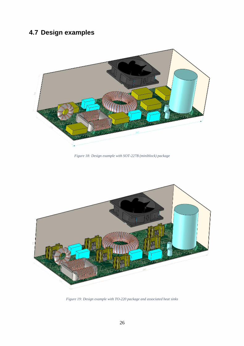
4.7 Design examples ........................................................................................................ 26
5 Conclusions ....................................................................................................................... 28
6 References ......................................................................................................................... 29

IV
List of Figures Figure 1: Proposed power supply showing clearly the five converter stages with the AC input
in the left and the DC output on the right ................................................................................... 1
Figure 2: MOSFET losses [9] .................................................................................................... 5
Figure 3: PFC demonstration which shows the line voltage and the absolute value of the input
current with and without PFC [12] ............................................................................................. 6
Figure 4: EMI filter example [10] .............................................................................................. 7
Figure 5: Standard EN55011 limit lines for conducted emissions on mains ports for Class B
equipment [3] ............................................................................................................................. 8
Figure 6: Full-wave rectifier [4] ................................................................................................. 8
Figure 7: Boost converter in operation [2] ................................................................................. 9
Figure 8: PWM generation [14] ............................................................................................... 10
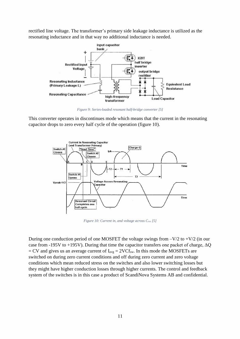
Figure 9: Series-loaded resonant half-bridge converter [5]...................................................... 11
Figure 10: Current in, and voltage across Cres [5] .................................................................... 11
Figure 11: Schematic of EMI-filter analysis [10] .................................................................... 12
Figure 12: Determination of corner frequencies [10] ............................................................... 13
Figure 13: Chart to find the smallest core from Magnetics according to power handling
capacity [8] ............................................................................................................................... 15
Figure 14: Adjustment of core winding according to DC bias level [8] .................................. 16
Figure 15: Magnetizing force versus magnetic flux density in Magnetics core 55735 (dark
green curve) [8] ........................................................................................................................ 17
Figure 16: Transformer short circuit test [13] .......................................................................... 18
Figure 17: Frequency versus magnetic flux density [7] ........................................................... 19
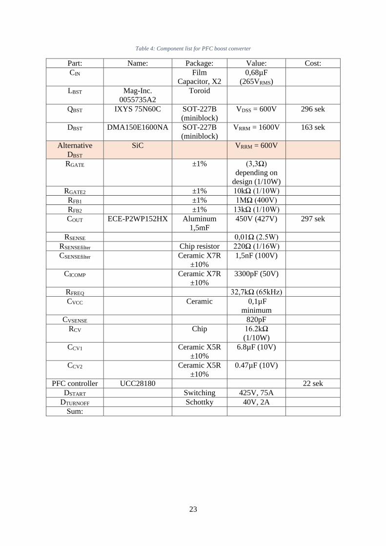
Figure 18: Design example with SOT-227B (miniblock) package .......................................... 26
Figure 19: Design example with TO-220 package and associated heat sinks ......................... 26
List of Tables Table 1: Table 1 is showing the basic parameters the calculations of the boost converter are
based on. ................................................................................................................................... 14
Table 2: Component list for the EMI-filter .............................................................................. 21
Table 3: Component list for the full-wave rectifier .................................................................. 21
Table 4: Component list for PFC boost converter .................................................................... 23
Table 5: Component list for the SLR half-bridge converter .................................................... 24
Table 6: Component list for the second full-wave rectifier...................................................... 25
Table 7: Energy efficiency results ............................................................................................ 25

1
1 Introduction 1.1 Background This 15hp bachelor work in electrical engineering is carried out at ScandiNova Systems AB in
Uppsala, Sweden. The company was founded in 2001 and their business is to build high-
quality pulse generators, so called modulators. These are used in several areas such as
radiation therapy, industrial radiography equipment, sterilization, and RADAR scientific
accelerator systems. The specifications of the pulses range between 1 kV ‒ 500 kV.
1.2 Aim Today the company produces its own power supplies to their larger modulators, but purchases
commercial power supplies for the smaller single-phase pulse generators called M0.5. Their
aim is to manufacture these by themselves in the company and this work is a theoretical study
to find some alternative solution for them for the future. High efficiency is a key parameter
since less power not only saves money directly but also indirectly by decreasing cooling costs
for the customer.
The company also needs to implement active PFC (power factor correction) in this device to
fulfill the EN61000–3–2 power factor regulation and reduce the line distortions and losses
that a low power factor causes by moving a lot of reactive energy between the source and the
sink.
1.3 Goal The goal parameters for the power supply are:
EN55011 standard in conducted disturbances in the 150 kHz – 30 MHz range
EN61000‒3‒2 standard power factor
95% energy efficiency
Single phase
1000W output with 100V ACRMS input (Japan etc.)
1500W output with 120V ACRMS input (North America etc.)
2000W output with 230V ACRMS input (Europe etc.)
Worldwide standard line input
~1500V DC output
1.4 Boundaries This work only contains the power supply and no other part of the modulator. The project is
only a theoretical work without the aim to build and test the designed converter. A design for
decreasing the radiated distortions that might appear is excluded as well as PCB layout.

2
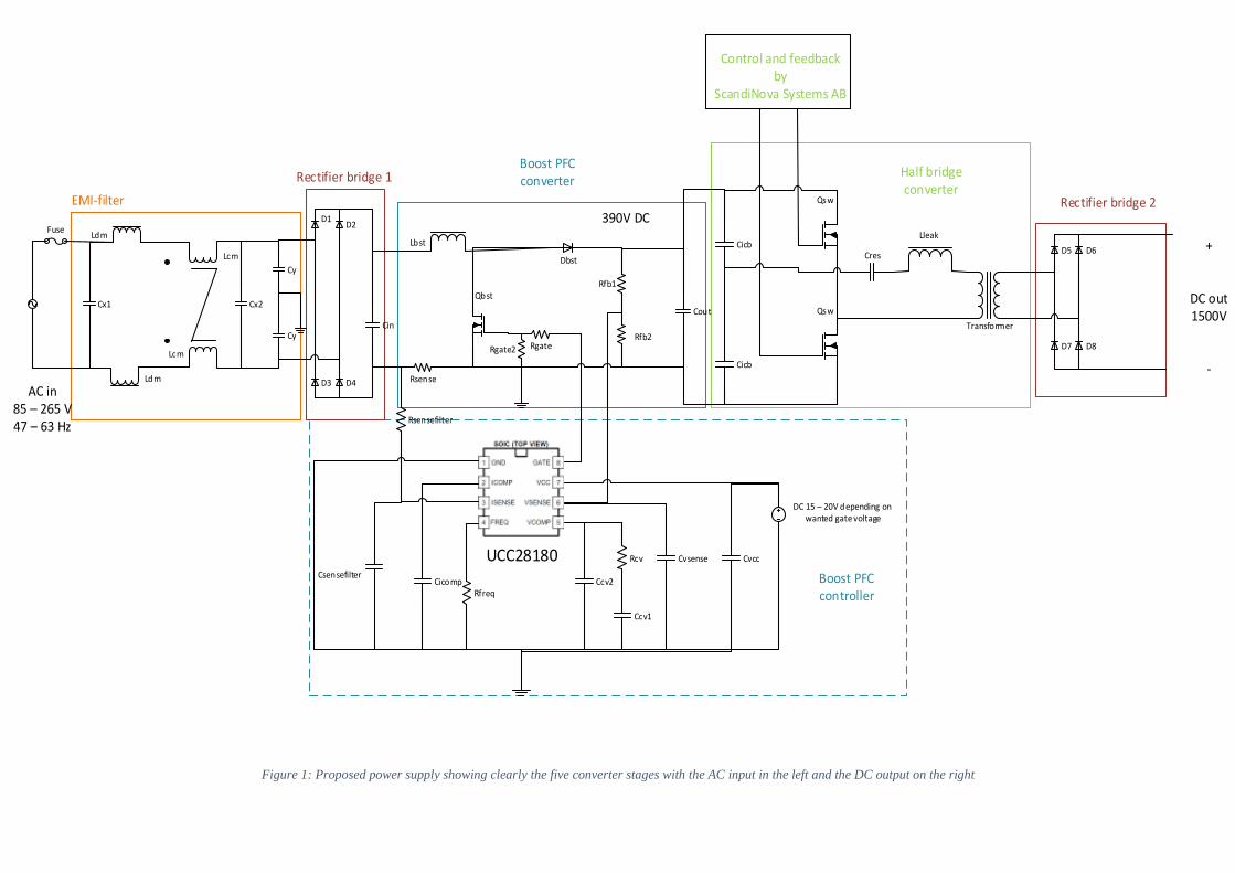
1.5 Design The power supply’s design (figure 1) is chosen according to energy efficiency, component
price and size of the current power supply.
The power supply is made of five parts which is an EMI-filter (section 2.4), two full-wave
rectifiers (section 2.5), a PFC boost converter with associated PFC controller (section 2.6) and
a SLR half-bridge converter (section 2.7). The voltage after the boost converter is ~390V and
after the half-bridge ~1500V. The boost converter has a switching frequency of 65 kHz and
the half-bridge 60 kHz to avoid interaction.
The step-up from line voltage was necessary and a boost converter with built-in PFC seemed
to be the best choice when it solves the world wide line input, PFC and make the step up to
390V in one solution. The company already had a fine working half-bridge solution. The
benefits with active PFC according to line losses versus energy efficiency of the power supply
can be discussed but should not affect when it is a way of handling the switch a little different
from a pure boost converter.
Cx1 Cx2
Ldm
Ldm
Lcm
Lcm
Cy
Cy
D1D2
D3 D4
UCC28180
Cin
Lbst
Qbst
Rgate
Dbst
Rfb1
Rfb2
Cout
Rsense
Rgate2
DC 15 – 20V depending on wanted gate voltage
CvccCvsense
Ccv2
Ccv1
Rcv
Rfreq
Rsensefilter
CicompCsensefilter
Cicb
Cicb
Qsw
Qsw
Transformer
Lleak
CresD5 D6
D7 D8
Control and feedback by
ScandiNova Systems AB
+
DC out1500V
-
Fuse
Rectifier bridge 1
EMI-filter Rectifier bridge 2
Half bridge converter
Boost PFC converter
390V DC
AC in85 – 265 V47 – 63 Hz
Boost PFC controller
Figure 1: Proposed power supply showing clearly the five converter stages with the AC input in the left and the DC output on the right

4
2 Theory 2.1 Origin of dominant power losses in a power supply
2.1.1 Wire The power loss in a conductor is defined as:
𝑃 = 𝐼2 · 𝑅 where 𝑅 = 𝜌 ·𝑙
𝐴 (1), (2)
From the definition (1) the power loss in a wire depends on how much current passes (I) and
the resistance (R) which depends on the length (l), the cross sectional area (A) and resistivity
(ρ).
2.1.2 Magnetic core The magnetic core has two main losses. One is hysteresis which occurs when the magnetic
field in the core is changing and the electrons have to move and align according to the new
and always changing magnetic field. The material’s BH-curve tells about the losses of one
cycle that are proportional to the area of the closed loop. The area is material dependent and
the losses will increase with higher frequencies when moving through the curve at a higher
rate per time unit. The other type of loss is eddy current losses which occur when a straight
magnetic field is varying in time and forces the electrons to circulate around it. The currents
produce heat through resistance in the material like the wire losses. A way to decrease the
circulating currents is to laminate the core in thin slices with insulating coating.
2.1.3 MOSFET In the MOSFET there are two type of losses. One is conduction loss like wire loss and occurs
because of the current and the resistivity from drain to source which is named RDS(ON) in the
datasheets. The second one is switching loss which can be defined as:
𝑃𝑠𝑤 = 𝑓𝑠𝑤 · (0.5 · 𝑉𝑜𝑢𝑡 · 𝐼𝑚𝑎𝑥(𝑡𝑟𝑖𝑠𝑒 + 𝑡𝑓𝑎𝑙𝑙) + 0.5 · 𝐶𝑜𝑠𝑠 · 𝑉𝑜𝑢𝑡2 ) (3)
Where trise and tfall is the rise and fall time and Coss = Cgd + Cds. COSS is referred to as the
transistor’s small signal output capacitance with the gate and source terminals shorted. Figure
2 describes the power loss of a MOSFET during one switching cycle.
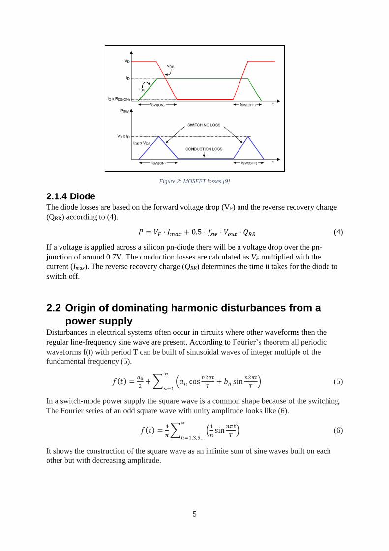
5
Figure 2: MOSFET losses [9]
2.1.4 Diode The diode losses are based on the forward voltage drop (VF) and the reverse recovery charge
(QRR) according to (4).
𝑃 = 𝑉𝐹 · 𝐼𝑚𝑎𝑥 + 0.5 · 𝑓𝑠𝑤 · 𝑉𝑜𝑢𝑡 · 𝑄𝑅𝑅 (4)
If a voltage is applied across a silicon pn-diode there will be a voltage drop over the pn-
junction of around 0.7V. The conduction losses are calculated as VF multiplied with the
current (Imax). The reverse recovery charge (QRR) determines the time it takes for the diode to
switch off.
2.2 Origin of dominating harmonic disturbances from a
power supply Disturbances in electrical systems often occur in circuits where other waveforms then the
regular line-frequency sine wave are present. According to Fourier’s theorem all periodic
waveforms f(t) with period T can be built of sinusoidal waves of integer multiple of the
fundamental frequency (5).
𝑓(𝑡) =𝑎0
2+ ∑ (𝑎𝑛 cos
𝑛2𝜋𝑡
𝑇+ 𝑏𝑛 sin
𝑛2𝜋𝑡
𝑇)
∞
𝑛=1 (5)
In a switch-mode power supply the square wave is a common shape because of the switching.
The Fourier series of an odd square wave with unity amplitude looks like (6).
𝑓(𝑡) =4
𝜋∑ (
1
𝑛sin
𝑛𝜋𝑡
𝑇)
∞
𝑛=1,3,5… (6)
It shows the construction of the square wave as an infinite sum of sine waves built on each
other but with decreasing amplitude.

6
2.3 Definition of power factor The input power factor is generally defined like (7).
𝑃𝑜𝑤𝑒𝑟 𝑓𝑎𝑐𝑡𝑜𝑟 (𝑃𝐹) = 𝑃 (𝑎𝑣𝑒𝑟𝑎𝑔𝑒/𝑟𝑒𝑎𝑙 𝑖𝑛𝑝𝑢𝑡 𝑝𝑜𝑤𝑒𝑟)
|𝑆| (𝑎𝑝𝑝𝑎𝑟𝑒𝑛𝑡 𝑖𝑛𝑝𝑢𝑡 𝑝𝑜𝑤𝑒𝑟)=
𝑃𝑑𝑐
𝑉𝑅𝑀𝑆·𝐼𝑅𝑀𝑆 (7)
Where Pdc is defined like (8).
𝑃𝑑𝑐 = 𝑉1_𝑅𝑀𝑆 · 𝐼1_𝑅𝑀𝑆 · cos (𝜑) (8)
Where V1_RMS and I1_RMS is the fundamental 50Hz or 60Hz sinusoidal waveform and cos (𝜑)
the displacement angle between the two. Because VRMS and V1_RMS are the same they can be
removed and the remaining is the power factor equation when current harmonics occurs in a
system (9).
𝑃𝐹 =𝐼1_𝑅𝑀𝑆
𝐼𝑅𝑀𝑆· cos(𝜑) (9)
The ratio between the RMS of the fundamental current and the total current is called
distortion power factor (10).
𝐷𝑖𝑠𝑡𝑜𝑟𝑡𝑖𝑜𝑛 𝑝𝑜𝑤𝑒𝑟 𝑓𝑎𝑐𝑡𝑜𝑟 = 𝐼1_𝑅𝑀𝑆
𝐼_𝑅𝑀𝑆 (10)
The power factor (9) was (for the case of a sinusoidal voltage) the product of the “distortion
power factor” and the “displacement power factor” cos (𝜑) where 0 is the case with no real
power transferred and 1 is the case with only real power transferred. Also a PF of less than 0
is possible when energy flows (in average) from the load to the source, i.e. during
regenerative braking of a motor.
Figure 3: PFC demonstration which shows the line voltage and the absolute value of the input current with and without PFC
[12]
The power factor correction tries to make a non-sinusoidal input current look as similar as the
sinusoidal input voltage as possible like the red curve (I_in with PFC) in figure 3
demonstrates to obtain a high power factor. In high power applications a high power factor is
necessary when the electric grid operators want the costumers to fulfill regulations such as the
EN61000-3-2 to maintain a high quality line with low reactive losses and disturbances. Even
for the costumer a high power factor is beneficial since smaller wires and lower level fuses
can be used.
7
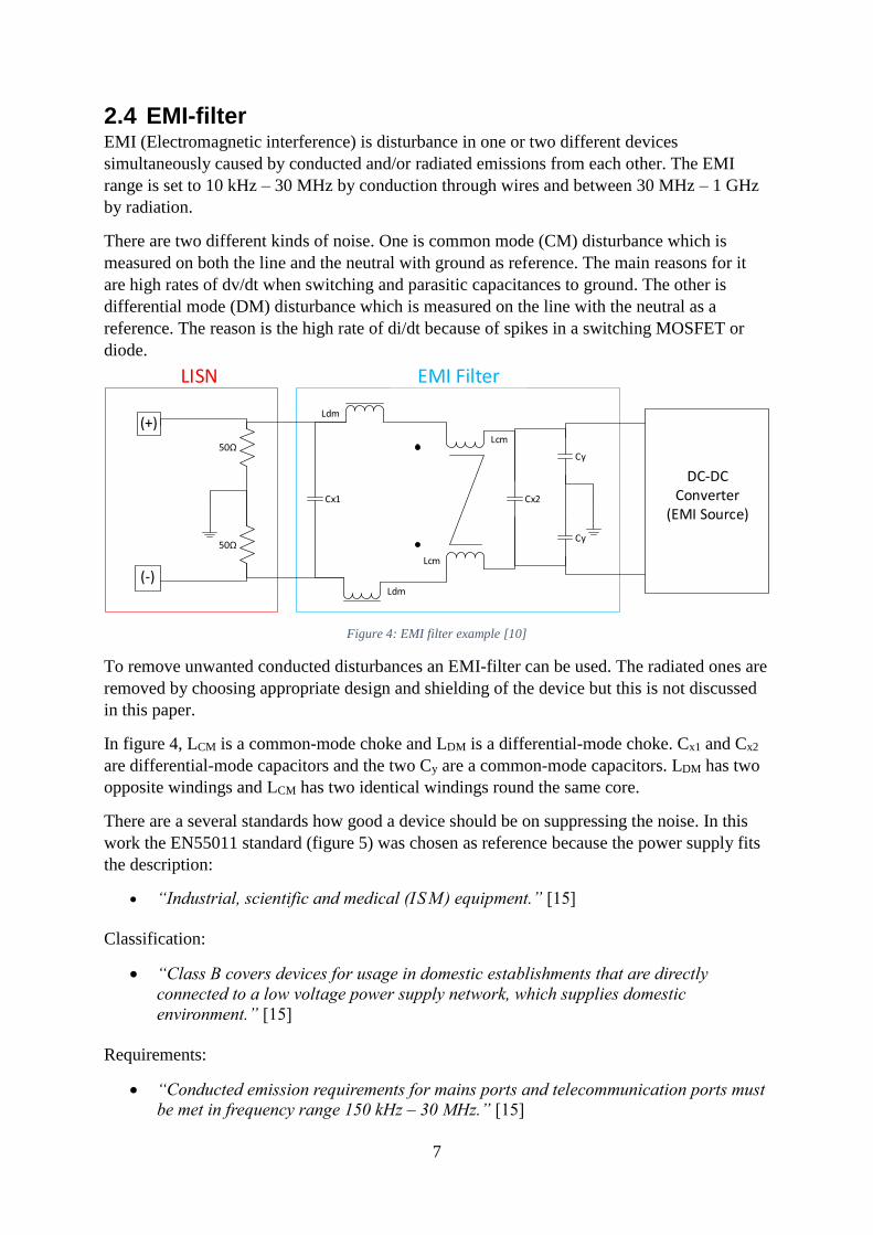
2.4 EMI-filter EMI (Electromagnetic interference) is disturbance in one or two different devices
simultaneously caused by conducted and/or radiated emissions from each other. The EMI
range is set to 10 kHz – 30 MHz by conduction through wires and between 30 MHz – 1 GHz
by radiation.
There are two different kinds of noise. One is common mode (CM) disturbance which is
measured on both the line and the neutral with ground as reference. The main reasons for it
are high rates of dv/dt when switching and parasitic capacitances to ground. The other is
differential mode (DM) disturbance which is measured on the line with the neutral as a
reference. The reason is the high rate of di/dt because of spikes in a switching MOSFET or
diode.
Cx1 Cx2
Ldm
Ldm
Lcm
Lcm
Cy
Cy
DC-DCConverter
(EMI Source)
50
50
(+)
(-)
LISN EMI Filter
Figure 4: EMI filter example [10]
To remove unwanted conducted disturbances an EMI-filter can be used. The radiated ones are
removed by choosing appropriate design and shielding of the device but this is not discussed
in this paper.
In figure 4, LCM is a common-mode choke and LDM is a differential-mode choke. Cx1 and Cx2
are differential-mode capacitors and the two Cy are a common-mode capacitors. LDM has two
opposite windings and LCM has two identical windings round the same core.
There are a several standards how good a device should be on suppressing the noise. In this
work the EN55011 standard (figure 5) was chosen as reference because the power supply fits
the description:
“Industrial, scientific and medical (ISM) equipment.” [15]
Classification:
“Class B covers devices for usage in domestic establishments that are directly
connected to a low voltage power supply network, which supplies domestic
environment.” [15]
Requirements:
“Conducted emission requirements for mains ports and telecommunication ports must
be met in frequency range 150 kHz – 30 MHz.” [15]

8
Figure 5: Standard E N55011 limit lines for conducted emissions on mains ports for Class B equipment [3]
2.5 Full-wave rectifier A full-wave rectifier contains four diodes with the needed voltage rating.
When an AC voltage source is connected to the full wave rectifier (figure 6) a diode pair only
conducts for positive voltage and blocks for negative voltage while the other diode pair does
the opposite. In order not to reduce the PF, a moderate sized smoothing capacitor is used that
allows us to receive a voltage ripple of around 6% [14] to have a reference when shaping the
input current for high power factor.
Figure 6: Full-wave rectifier [4]
9
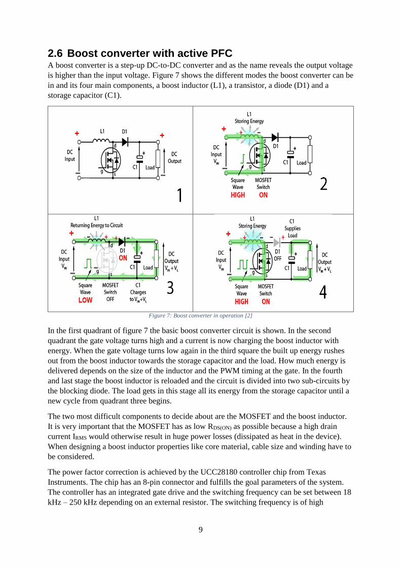
2.6 Boost converter with active PFC A boost converter is a step-up DC-to-DC converter and as the name reveals the output voltage
is higher than the input voltage. Figure 7 shows the different modes the boost converter can be
in and its four main components, a boost inductor (L1), a transistor, a diode (D1) and a
storage capacitor (C1).
Figure 7: Boost converter in operation [2]
In the first quadrant of figure 7 the basic boost converter circuit is shown. In the second
quadrant the gate voltage turns high and a current is now charging the boost inductor with
energy. When the gate voltage turns low again in the third square the built up energy rushes
out from the boost inductor towards the storage capacitor and the load. How much energy is
delivered depends on the size of the inductor and the PWM timing at the gate. In the fourth
and last stage the boost inductor is reloaded and the circuit is divided into two sub-circuits by
the blocking diode. The load gets in this stage all its energy from the storage capacitor until a
new cycle from quadrant three begins.
The two most difficult components to decide about are the MOSFET and the boost inductor.
It is very important that the MOSFET has as low RDS(ON) as possible because a high drain
current IRMS would otherwise result in huge power losses (dissipated as heat in the device).
When designing a boost inductor properties like core material, cable size and winding have to
be considered.
The power factor correction is achieved by the UCC28180 controller chip from Texas
Instruments. The chip has an 8-pin connector and fulfills the goal parameters of the system.
The controller has an integrated gate drive and the switching frequency can be set between 18
kHz – 250 kHz depending on an external resistor. The switching frequency is of high

10
importance when it comes to switch losses. Higher frequency gives higher losses but stands
against more bulky components and in the end the size of the power supply.
Power factor correction is a way of suppressing the harmonics close to the fundamental (line)
frequency if the application has an uneven current consumption. The EMI-filter aims at
removing the disturbances at high frequencies and the PFC-circuit tries to remove low
frequency input current harmonics in order to decrease power line losses.
The selected UCC28180 controller chip operates under Continuous Conduction Mode (CCM).
It means that the inductor current flow never stops but stays on a high level almost in every
condition. This mode is popular in higher power levels as it has low peak and RMS current.
This reduces stress in the MOSFET, diode and inductor. Designing the EMI-filter and boost
inductor is easier because of the continuous current and the fixed switching frequency [6].
The control- and feedback system is of a newer predictive average current mode type which
decreases the external number of components and complexity. The PWM modulator gets its
feedback from the voltage drop over the sense resistor and the 5V comparative voltage from
the output voltage. The PWM stage generates a periodic ramp function (figure 8) and makes
the gate voltage high whenever the ramp voltage exceeds the VICOMP voltage and low for the
opposite. The ramp/VICOMP intersection determines the off timing, and hence duty cycle off
ratio. Since DutyOFF = VIN/VOUT by the boost topology equation, VIN is sinusoidal and VICOMP
is proportional to the boost inductor current. It follows that the control loop forces the average
inductor current to follow the input voltage wave-shape to maintain boost regulation [14]. In
this way the controller can match the input sine wave without separate line sensing input.
Figure 8: PWM generation [14]
2.7 Series-loaded resonant half bridge converter The step-up after the boost converter is a SLR (Series-Loaded Resonant) half-bridge
converter (figure 9) with a high frequency transformer followed by a (second) full-wave
rectifier. The name series-loaded is because the load always appears to be in series with the
LC resonant tank. The maximum output voltage is the transformer ratio times half of the
11
rectified line voltage. The transformer’s primary side leakage inductance is utilized as the
resonating inductance and in that way no additional inductance is needed.
Figure 9: Series-loaded resonant half-bridge converter [5]
This converter operates in discontinues mode which means that the current in the resonating
capacitor drops to zero every half cycle of the operation (figure 10).
Figure 10: Current in, and voltage across Cres [5]
During one conduction period of one MOSFET the voltage swings from –V/2 to +V/2 (in our
case from -195V to +195V). During that time the capacitor transfers one packet of charge, ΔQ
= CV and gives us an average current of Iavg = 2VCfsw. In this mode the MOSFETs are
switched on during zero current conditions and off during zero current and zero voltage
conditions which mean reduced stress on the switches and also lower switching losses but
they might have higher conduction losses through higher currents. The control and feedback
system of the switches is in this case a product of ScandiNova Systems AB and confidential.

12
3 Method and design This is the method and design section which is showing the approaches of how to calculate
this power supply’s components and energy losses.
3.1 How to calculate an EMI-filter A device called LISN (Line Impedance Stabilization Network) is connected between the AC
input and the equipment under test. The main reasons to use it is that it filters disturbance of
higher frequency than line frequency, creates a known impedance for the equipment under
test and gives a connection where you can connect a spectrum analyzer (figure 11).
Figure 11: Schematic of EMI-filter analysis [10]
The common mode noise will see two 50Ω resistors in parallel while differential noise sees
two 50Ω resistors in series. The spectrum analyzer receives the total conducted noise from
LISN and it needs to be separated into CM and DM components.
VLINE = VCM + VDM
VNEUTRAL = VCM - VDM
VCM = (VLINE + VNEUTRAL)/2
VDM = (VLINE - VNEUTRAL )/2
There is a good procedure how to accomplish a filter that gives the wanted result [10].
Measure the differential- and common mode noise levels
Determine the differential- and common mode attenuation requirements using o (Vreq, CM)dB = (VCM, measured)dB – (Vlimit)dB + 6dB safety margin o (Vreq, DM)dB = (VDM, measured)dB – (Vlimit)dB + 6dB safety margin
Determine the corner frequency by drawing a 40 dB/Dec slope which is tangent to the required attenuation for DM and CM at 150kHz (figure 12)
Calculate component values
13
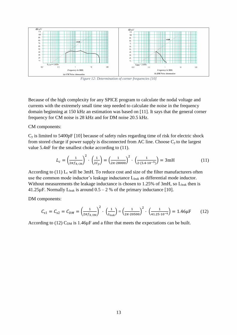
Figure 12: Determination of corner frequencies [10]
Because of the high complexity for any SPICE program to calculate the nodal voltage and
currents with the extremely small time step needed to calculate the noise in the frequency
domain beginning at 150 kHz an estimation was based on [11]. It says that the general corner
frequency for CM noise is 28 kHz and for DM noise 20.5 kHz.
CM components:
Cy is limited to 5400pF [10] because of safety rules regarding time of risk for electric shock
from stored charge if power supply is disconnected from AC line. Choose Cy to the largest
value 5.4nF for the smallest choke according to (11).
𝐿𝑐 = (1
2𝜋𝑓R, CM)
2
· (1
2𝐶𝑦) = (
1
2𝜋·28000)
2
· (1
2·(5.4·10−9)) = 3mH (11)
According to (11) Lc will be 3mH. To reduce cost and size of the filter manufacturers often
use the common mode inductor’s leakage inductance Lleak as differential mode inductor.
Without measurements the leakage inductance is chosen to 1.25% of 3mH, so Lleak then is
41.25µF. Normally Lleak is around 0.5 – 2 % of the primary inductance [10].
DM components:
𝐶x1 = 𝐶x2 = 𝐶𝐷𝑀 = (1
2𝜋𝑓R, DM)
2
· (1
𝐿leak) = (
1
2𝜋·20500)
2
· (1
41.25·10−6) = 1.46µF (12)
According to (12) CDM is 1.46µF and a filter that meets the expectations can be built.

14
3.2 Boost converter with active PFC The calculation of the boost converter components are made with reference to the TI
UCC28180 datasheet [14] and the UCC28180 Microsoft Excel design guide. Table 1 is
showing the basic parameters the calculations of the boost converter are based on. The input
voltage is varying within the values set by the expected environment of the power supply.
Table 1: Table 1 is showing the basic parameters the calculations of the boost converter are based on.
Japan USA Europe
min std max min std max min std max
Input voltage [VRMS]: 85 100 110 108 120 132 207 230 265
Max output power [W]: 1025 1025 1025 1525 1525 1525 2025 2025 2025
Output voltage [V]: 390 390 390 390 390 390 390 390 390
Max output current [I]: 2.63 2.63 2.63 3.91 3.91 3.91 5.19 5.19 5.19
Expected power factor:
0.99 0.99 0.99 0.99 0.99 0.99 0.99 0.99 0.99
Expected efficiency: 0.95 0.95 0.95 0.95 0.95 0.95 0.95 0.95 0.95
3.2.1 Design of boost inductor for CCM operation The calculation of the boost inductor starts with the selection of basic properties:
The switching frequency is 65 kHz because of a good compromise between the size of the
boost inductor and the switching losses.
The material of the core is made of MPP material because of its low losses and good
inductance stability in DC bias conditions.
The inductance is chosen with help of equation 28 in [14] with a current ripple of 3.33A
which is 15-25% of max input current which was recommended [14]. The inductance is
450µH.
Maximum inductor current is 22.9A and occurs when having a low (108V) input voltage at
1500W max output according to equation (6) and (26) in [14].
With these parameters, we can calculate the LI2-product which is a measure of the energy
storage and needs to be fulfilled for proper function of the inductor (13).
𝐿𝐼2 = 236mHA2 (13)
According to figure 13 the smallest core from Magnetics that fits the LI2 product can be
selected and it seems that the core 55735 is a good choice.

15
Figure 13: Chart to find the smallest core from Magnetics according to power handling capacity [8]
The datasheet of the core gives the following information. Permeability is 26µ and AL = 88 ±
8% where the AL (nH/turns2) value is a nominal value of inductance.
𝐴𝐿𝑚𝑖𝑛 = 88nH/turns2 − 8% = 81nH/turns2 (14)
Then the number of turns (N) that is needed for the required inductance is calculated (15).
𝑁 = √𝐿𝑟𝑒𝑞
𝐴𝐿 𝑚𝑖𝑛= 74.5 turns (15)
Now the DC bias level of the core can be calculated. 𝑙𝑒 is the average core path in
centimeters.
𝐻 =𝑁∗𝐼
𝑙𝑒=
74.5 turns · 22.9A
18.4 cm= 92.77 A·turns/cm (16)

16
Figure 14: Adjustment of core winding according to DC bias level [8]
The next step is to correct the DC bias level according to the core environment (figure 14).
𝑁 =74.5 𝑡𝑢𝑟𝑛𝑠
0.86= 87 turns (17)
This gives a new 𝐻 = 108.3 A·turns/cm and a correction factor of the AL-value of 0.8.
𝐿 = 𝑁2𝐴𝐿 = 490µH (18)
According to the new AL = 81 ∙ 0.8 = 64.8 nH/turns2 the environmental adjustments are ready
and give an inductance of 490µH versus the required 450µH which means OK.
The “right” wire size can now be chosen by a wire table [8]. A thicker wire has lower
resistance but results in a larger and heavier inductor. An AWG 10 magnet wire was chosen
that has a resistance of 3.28mΩ/m.
The fill factor is a measure of how much the center of the toroid is taken by winding. The
recommendation is 30 – 45 % [8].
fillfactor = 𝑁𝐴𝑤
𝑊𝑎=
87 turns ∙ 0.056cm2
15.cm2 = 31.5% (19)
Where Aw is the cross sectional area of the wire and Wa is the core window area. The
recommended 30 – 45 % fill factor is fulfilled with a good capability wire. As a test the
magnetic flux density was calculated to know if the saturation limit was close (20).
𝐵 = 𝑁𝐼µ0µ𝑟
𝑙 (20)
The result was 0.35 T which fulfills the 0.75 T saturation limit for the MMP material.
17
Loss calculation:
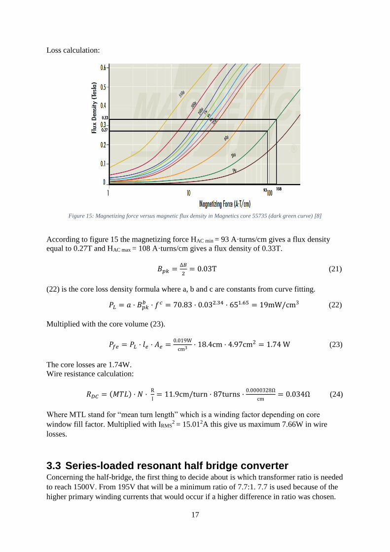
Figure 15: Magnetizing force versus magnetic flux density in Magnetics core 55735 (dark green curve) [8]
According to figure 15 the magnetizing force HAC min = 93 A·turns/cm gives a flux density
equal to 0.27T and HAC max = 108 A·turns/cm gives a flux density of 0.33T.
𝐵𝑝𝑘 =∆𝐵
2= 0.03T (21)
(22) is the core loss density formula where a, b and c are constants from curve fitting.
𝑃𝐿 = 𝑎 · 𝐵𝑝𝑘𝑏 · 𝑓𝑐 = 70.83 · 0.032.34 · 651.65 = 19mW/cm3 (22)
Multiplied with the core volume (23).
𝑃𝑓𝑒 = 𝑃𝐿 · 𝑙𝑒 · 𝐴𝑒 =0.019W
cm3 · 18.4cm · 4.97cm2 = 1.74 W (23)
The core losses are 1.74W.
Wire resistance calculation:
𝑅𝐷𝐶 = (𝑀𝑇𝐿) · 𝑁 · R
l= 11.9cm/turn · 87turns ·
0.0000328Ω
cm= 0.034Ω (24)
Where MTL stand for “mean turn length” which is a winding factor depending on core
window fill factor. Multiplied with IRMS2
= 15.012A this give us maximum 7.66W in wire
losses.
3.3 Series-loaded resonant half bridge converter Concerning the half-bridge, the first thing to decide about is which transformer ratio is needed
to reach 1500V. From 195V that will be a minimum ratio of 7.7:1. 7.7 is used because of the
higher primary winding currents that would occur if a higher difference in ratio was chosen.

18
The switching frequency is set to be 60 kHz and the resonance frequency is set to be 60
kHz/0.85 = 70588Hz. This is to operate the converter in discontinues current mode as wanted
in order to guarantee soft-switching of the power transistors. A resonance frequency ~15%
above switching frequency is recommended and used in other ScandiNova Systems
converters [5]. 60 kHz was chosen to separate it from the boost converters 65 kHz as a quest
to decrease distortion. According to [5]
𝐶res =𝑁ratio𝑃out
2𝑉DCin𝑉load𝑓switch=
7.7·2000𝑊
2·390𝑉·1500𝑉·60000𝐻𝑧= 0.219µF (25)
𝐿res =1
(2𝜋𝑓res)2𝐶res=
1
(2·𝜋·70588𝐻𝑧)2·0.219µ𝐹= 23.17µH (26)
VDCin is the full DC voltage (390V) input. For this converter the resonance capacitor is
0.219µF and the leakage inductance of the transformers primary winding has to be most
23.17µH (25), (26).
𝐼avg. pri. = 2𝐶𝑟𝑒𝑠𝑉𝐷𝐶𝑖𝑛𝑓switch = 2 · 0.219µF · 390V · 60kHz = 10.26A (27)
𝐼peak =𝜋𝐶𝑟𝑒𝑠𝑉DCin
2𝑇1=
𝜋·0.219µ𝐹·390𝑉
2·(
170588
)
2
= 18.97A (28)
𝐼RMS =𝐼peak
√2√
2𝑇1
𝑇3=
18.97𝐴
√2· √2·
(1
70588)
2
(1
60000)
= 12.37A (29)
According to equation (27), (28), and (29) the primary currents are calculated and can then be
divided by 7.7 to have the secondary currents. T1 is the time of one delivered charge packet Q
and T3 is the period time of the switching frequency (figure 10).
3.3.1 How to measure primary leakage inductance To find the transformers leakage inductance a so called short circuit test is made on the
transformer.
Figure 16: Transformer short circuit test [13]
Figure 16 shows the connection diagram for the short circuit test. In this case the high voltage
side of the transformer is short circuited and a wattmeter (W), voltmeter (V) and amperemeter
(A) are connected on the low voltage side of the transformer. A voltage is applied to the low
voltage side and increased from zero until the amperemeter reading is equal to the rated
current of the transformer.
The amperemeter reading gives the primary equivalent of full load current (Isc). The voltage
applied for full load current is very small compared to the rated voltage. Hence, core loss due
to small applied voltage can be neglected, (Rp and Xp). The wattmeter reading can be taken as
19
copper loss in the transformer primary windings. Therefore, W = Isc2Req, where Req is the
equivalent resistance in the windings. Because Zeq = Vsc/Isc, the equivalent reactance of the
transformer can be calculated from the formula Zeq2 = Req
2 + Xeq2.
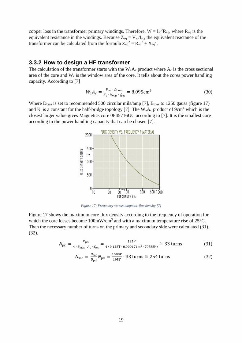
3.3.2 How to design a HF transformer The calculation of the transformer starts with the WaAc product where Ac is the cross sectional
area of the core and Wa is the window area of the core. It tells about the cores power handling
capacity. According to [7]
𝑊𝑎𝐴𝑐 =𝑃out ∙ 𝐷𝑐𝑚𝑎
𝐾𝑡 ∙ 𝐵𝑚ax ∙ 𝑓res= 8.095cm4 (30)
Where Dcma is set to recommended 500 circular mils/amp [7], Bmax to 1250 gauss (figure 17)
and Kt is a constant for the half-bridge topology [7]. The WaAc product of 9cm4 which is the
closest larger value gives Magnetics core 0P45716UC according to [7]. It is the smallest core
according to the power handling capacity that can be chosen [7].
Figure 17: Frequency versus magnetic flux density [7]
Figure 17 shows the maximum core flux density according to the frequency of operation for
which the core losses become 100mW/cm3 and with a maximum temperature rise of 25°C.
Then the necessary number of turns on the primary and secondary side were calculated (31),
(32).
𝑁pri =𝑉pri
4 ∙ 𝐵max ∙ 𝐴𝑐 ∙ 𝑓res=
195𝑉
4 ∙ 0.125T · 0.000171m2 · 70588Hz≅ 33 turns (31)
𝑁sec = 𝑈sec
𝑈pri𝑁pri =
1500𝑉
195𝑉· 33 turns ≅ 254 turns (32)

20
This gives a primary winding of 33 turns and a secondary winding of 254 turns. If a primary
winding wire with a cross sectional area of 5.6mm2 (American Wire Gauge, AWG 10) and a
secondary winding wire with a cross sectional area of 0.754mm2 (AWG 19) the core window
fill factor can be obtained.
𝐾𝑊𝑎 ≥ 𝑁𝑝𝐴wp + 𝑁𝑠𝐴ws (33)
Where K is a constant of maximum recommended fill factor 0.6 (60%) of the core window
area Wa.
0.6 · 8.618cm2 ≥ 33 · 0.056cm2 + 254 · 0.00754cm2 (34)
5.17cm2 ≥ 3.76cm2 (35)
3.76cm2 8.618cm2⁄ = 44% fill factor (36)
A fill factor of 44% is within the recommended 60% and OK. According to figure 17 this
example is based on a core design with losses of 100mW/cm3 and according to the datasheet
the core volume is 27.9 cm3 and this give a power loss of 2.79W.

21
4 Results and discussion Most of the design parameters were made by hand according to [14], but with a little help of
TI’s UCC28180 design calculator in Microsoft Excel. A lot of time the design calculator
could not be used because of wrong calculated currents when it was chosen to have different
maximum output power according to different line voltages.
This project was not reasonable to simulate because of huge time consuming analysis and
complex control systems but the work can be considered realistic.
4.1 EMI-filter All the components to build the EMI-filter are found in table 2.
Table 2: Component list for the EMI-filter
Part: Name: Package: Value: Cost:
Cx1 1.46µF
LCM Wurth
7448052303
3mH 125 sek
LDM 41.25µH
Cx2 1.46µF
2 x Cy 5.4nF
Sum:
4.2 Full-wave rectifier The first full-wave rectifier turns a lot of energy into heat because of the low voltage and the
high currents. The maximum average output current of the bridge is 11.54A in Japan, 13.52A
in the USA and 9.36A in Europe. The rectifier diodes have a voltage drop of 1.1V at these
currents. It gives a power loss of 25.4W, 29.75W and 20.6W. Even if the voltage drop is 1V it
just makes a small difference. Table 3 shows the component list of the full-wave rectifier.
Table 3: Component list for the full-wave rectifier
Part: Name: Package: Value: Cost:
Rectifier bridge 1 IXYS VBO40-
08NO6
SOT-227B
(miniblock)
VRRM = 800V 145 sek
Sum: 145 sek

22
4.3 Boost converter with active PFC The boost converter was chosen because of the amount of examples of good feasibility with
implementation of PFC. The microcontroller UCC28180 was chosen because of its simplicity
and good reviews on its precursors (UCC28019 and UCC28019A). It is also meeting the
demands of the converter and the switching frequency is changeable for best modifiability
later in the work if the frequency interferes with the other switches when testing. A
calculation on a core with 62mm (0055615A2) outer diameter that could work was made but
came up with a fill factor of above 60%. The bigger core is better when it comes to
modification opportunities when litz wire might be needed because of high skin effect in the
magnet wire.
It is difficult to know if the power factor correction really helps to decrease the general energy
consumption compared it was not used. But for sure the power supply was in need of a step-
up from the line voltage anyway and PFC is only a way to handle the switch a little different.
Probably the same losses should have occurred anyway.
Table 4 shows the component list of the PFC boost converter.
23
Table 4: Component list for PFC boost converter
Part: Name: Package: Value: Cost:
CIN Film
Capacitor, X2
0,68µF
(265VRMS)
LBST Mag-Inc.
0055735A2
Toroid
QBST IXYS 75N60C SOT-227B
(miniblock)
VDSS = 600V 296 sek
DBST DMA150E1600NA SOT-227B
(miniblock)
VRRM = 1600V 163 sek
Alternative
DBST
SiC VRRM = 600V
RGATE ±1% (3,3Ω)
depending on
design (1/10W)
RGATE2 ±1% 10kΩ (1/10W)
RFB1 ±1% 1MΩ (400V)
RFB2 ±1% 13kΩ (1/10W)
COUT ECE-P2WP152HX Aluminum
1,5mF
450V (427V) 297 sek
RSENSE 0,01Ω (2.5W)
RSENSEfilter Chip resistor 220Ω (1/16W)
CSENSEfilter Ceramic X7R
±10%
1,5nF (100V)
CICOMP Ceramic X7R
±10%
3300pF (50V)
RFREQ 32,7kΩ (65kHz)
CVCC Ceramic 0,1µF
minimum
CVSENSE 820pF
RCV Chip 16.2kΩ
(1/10W)
CCV1 Ceramic X5R
±10%
6.8µF (10V)
CCV2 Ceramic X5R
±10%
0.47µF (10V)
PFC controller UCC28180 22 sek
DSTART Switching 425V, 75A
DTURNOFF Schottky 40V, 2A
Sum:

24
4.4 Series-loaded resonant half bridge converter The resonant half bridge was chosen mostly because the company already uses this topology
in their other modulators with good results. The control and feedback system for two switches
exists and can be implemented fast. A transformer ratio of 7.7:1 was chosen. The ratio should
not be set to high because of the increased primary currents that will occur. It gives us a
maximum average current at 10.3A. The RDS(ON) of the chosen MOSFETs is 14.5mΩ. 10.3A2
· 0.0145Ω = 1.54W in conduction losses. The switching losses are considered low because of
the soft switching with help of the resonant tank. The wanted transformer design was two C
shape halves put together and the general power transformer low-mid frequency material P
was chosen. The “right” core for the application became 0P45716UC with a fill factor of 44%
which is within the recommended 60%. Even in the transformer it is more room for usage of
litz wire instead of magnet wire.
According to the table the core losses should be 100mW/cm3. The volume of the core is
27.9cm3.
100mW/cm3 · 27.9 cm3 = 2.79W (37)
A way to archive the right leakage inductance is to make the transformer as good as it gets
and then use a small air core inductor to increase it to the required 23.17µH. The difficulties
with the transformer are a disadvantage of the resonant half bridge. If there was not any half
bridge driver ready to use, a regular full bridge would be a good choice according to power
level and power losses. A full bridge just has half the primary current because of full usage of
the voltage drop to ground [1], although the driver timings can be difficult when two switch
couples have to open and close simultaneously.
Table 5 shows the component list of the SLR half-bridge converter.
Table 5: Component list for the SLR half-bridge converter
Part: Name: Package: Value: Cost:
2 x QSW IXYS
IXFN210N30P3
SOT-227B
(miniblock)
VDSS = 300V 2 x 245 sek
Transformer 2 x Mag-Inc.
0P45716UC
UR shape cores
2 x CICB 2 x 2.7µF (min
250V)
CRES 0.219µF (min
250V)
LLEAK 23.17µH leakage
Sum:

25
4.5 Second full-wave rectifier The maximum RMS current reaches to 1.6A at 2kW and the forward voltage drop is then
0.9V. It gives a power loss of 2 · 0.9V · 1.6A = 2.88W total losses in the rectifier.
Component list in table 6.
Table 6: Component list for the second full-wave rectifier
Part: Name: Package: Value: Cost:
Rectifier bridge 2 IXYS
VBO40-
16NO6
SOT-227B
(miniblock)
VRRM = 1600V 150 sek
Alternative bridge SiC VRRM = 1600V
Sum: 150 sek
4.6 Energy efficiency results
Table 7: Energy efficiency results
Losses (W):
100VRMS
(1000W)
120VRMS
(1500W)
230VRMS
(2000W)
First diode bridge 25,4 29,75 20,6
Bst inductor winding 5,59 7,66 3,68
Bst inductor core 1,74 1,74 1,74
Bst MOSFET 15,04 17,53 10,69
Bst diode 2,37 3,52 4,67
Bst Rsense 1,64 2,26 1,08
HB 2 x MOSFET 17,5 17,5 17,5
HB transformer
winding 0,5 1 2
HB transformer core 2,79 2,79 2,79
Second diode bridge 1,44 2,16 2,88
Total 74,01 85,91 67,63
Efficiency 93% 94% 96%
Table 7 shows max load, worst case energy efficiency at three different part of the world. The
goal was to reach an efficiency of 95%. This design and components get very close by having
really good switching diodes with close to zero revers recovery like the Silicon Carbide (SiC)
type. They are more expensive but will manage the work as boost diode and second half
bridge better. Two parts are marked in the component list and it might be recommended to
look at alternatives for these. Why it was not chosen from the beginning was a wish to use the
power supply steel box as a heat sink, then SOT-227B is a good package and the fact that no
SiC components with SOT-227B package was found. They usually use some kind of TO-220
similarities and that is why two different designs in SolidWorks was made (figure 18 and 19).
26
4.7 Design examples
Figure 18: Design example with SOT-227B (miniblock) package
Figure 19: Design example with TO-220 package and associated heat sinks

27
Figure 18 and 19 show two different designs that are made in SolidWorks with respect to the
size of the current power supply (341mm × 135mm × 88mm) and “as close as possible” size
of the components in the component lists. According to figure 18 and 19 all the components
fit but this needs to be confirmed with a proper PCB design.

28
5 Conclusions The outcome of this project is a single phase power supply design with PFC that can be used
all over the world and that meets the EN61000-3-2 standard of current harmonics. The voltage
output will be ~1500V. The conducted EMI disturbances that can occur are removed with a
second order low pass filter to meet the EN55011 standard. A physical design is made in
SolidWorks on present power supply’s size and according to the size of the proposed
components in the component list. The design works according to required space. An energy
efficiency calculation is made by datasheet values and equations and meets the aim of 95%
energy efficiency in most cases. A test built is necessary before production.

29
6 References
[1] Abdel-Rahman, S. (2012, September ). Retrieved from
http://www.infineon.com/dgdl/Application_Note_Resonant+LLC+Converter+Operati
on+and+Design_Infineon.pdf?folderId=db3a30431a5c32f2011a77f9c03e6cb4&fileId
=db3a30433a047ba0013a4a60e3be64a1
[2] Boost topology. (n.d.). Retrieved from learnabout-electronics: http://www.learnabout-
electronics.org/PSU/psu32.php
[3] EN55011 standard. (n.d.). Retrieved from RfEmcDevelopment:
http://rfemcdevelopment.eu/images/Standard_images/EN55011/CE_55011_B.jpg
[4] Full wave rectifier. (n.d.). Retrieved from i.stack.imgur:
http://i.stack.imgur.com/BLGnf.gif
[5] Inc., C. E. (2004). ScandiNova Systems AB paper.
[6] Joel Turchi, D. D. (2014, April). Retrieved from
http://www.onsemi.com/pub_link/Collateral/HBD853-D.PDF
[7] Magnetics Inc. (n.d.). Retrieved from Ferrite core catalog: http://www.mag-
inc.com/File%20Library/Product%20Literature/Ferrite%20Literature/Magnetics2013F
erriteCatalog.pdf
[8] Magnetics Inc. (n.d.). Retrieved from Powder core catalog: http://www.mag-
inc.com/File%20Library/Product%20Literature/Powder%20Core%20Literature/Mage
nticsPowderCoreCatalog2013Update.pdf
[9] MOSFET Losses. (n.d.). Retrieved from Maximintegrated:
http://www.maximintegrated.com/en/images/appnotes/4266/4266Fig04.gif
[10] Nasser, N. Y. (2012, March). Practical Approach in Designing Conducted EMI Filter
to Mitigate Common Mode and Differential Mode Noises in SMPS. Journal of
Engineering and Development, 16.
[11] P. Ram Mohan, M. V. (2008, 10 22). Simulation of a Boost PFC Converter with
Electro Magnetic Interference Filter. World Academy of Science, Engineering and
Technology, 2, 738.
[12] PFC demonstration. (n.d.). Retrieved from Schockpower:
http://www.schockpower.com/pics/Pfc.jpg
[13] Short Circuit Test. (n.d.). Retrieved from Wikipedia:
http://upload.wikimedia.org/wikipedia/commons/1/15/Short_Circuit_test.jpg
[14] Texas Instruments Inc. (2013, November). Retrieved from Product document,
UCC28180: http://www.ti.com/lit/gpn/ucc28180
[15] EN 55011:2009 standard. Retrieved from RF EMC Development:
dd.d…dhttp://rfemcdevelopment.eu/en/emc-emi-standards/en-55011-2009