The synthesis and characterization of Cu2ZnSnS4 thin films ...
11
ELECTRONIC MATERIALS The synthesis and characterization of Cu 2 ZnSnS 4 thin films from melt reactions using xanthate precursors Mundher Al-Shakban 1 , Peter D. Matthews 2 , Nicky Savjani 2 , Xiang L. Zhong 1 , Yuekun Wang 3 , Mohamed Missous 3 , and Paul O’Brien 1,2, * 1 School of Materials, University of Manchester, Oxford Road, Manchester M13 9PL, UK 2 School of Chemistry, University of Manchester, Oxford Road, Manchester M13 9PL, UK 3 School of Electrical and Electronic Engineering, University of Manchester, Oxford Road, Manchester M13 9PL, UK Received: 4 May 2017 Accepted: 6 July 2017 Published online: 20 July 2017 Ó The Author(s) 2017. This article is an open access publication ABSTRACT Kesterite, Cu 2 ZnSnS 4 (CZTS), is a promising absorber layer for use in photo- voltaic cells. We report the use of copper, zinc and tin xanthates in melt reac- tions to produce Cu 2 ZnSnS 4 (CZTS) thin films. The phase of the as-produced CZTS is dependent on decomposition temperature. X-ray diffraction patterns and Raman spectra show that films annealed between 375 and 475 °C are tetragonal, while at temperatures \ 375 °C hexagonal material was obtained. The electrical parameters of the CZTS films have also been determined. The con- duction of all films was p-type, while the other parameters differ for the hexagonal and tetragonal materials: resistivity (27.1 vs 1.23 X cm), carrier con- centration (2.65 9 10 ?15 vs 4.55 9 10 ?17 cm -3 ) and mobility (87.1 vs 11.1 cm 2 - V -1 s -1 ). The Hall coefficients were 2.36 9 10 3 versus 13.7 cm 3 C -1 . Introduction Copper zinc tin sulfide (Cu 2 ZnSnS 4 , CZTS) is a promising absorber layer for use in photovoltaic cells and is composed of low toxicity [1–3] and earth- abundant elements [4–6]. It has a large absorption coefficient (a C 10 4 cm -1 ) and a direct band gap of about 1.45 eV [7–10]. The performance of CZTS absorber layers is still less than that of silicon [11], which is the current industrial standard; however, unlike silicon, it has the advantage of a direct and tunable band gap [12]. CZTS thin films have been prepared using several techniques, including: chemical vapor deposition (CVD) [13], co-sputtering followed by sulfurization from the vapor phase [14], chemical bath deposition (CBD) [15], successive ionic layer adsorption and reaction (SILAR) [16] and solvothermal treatment of a layered elemental (copper, zinc and tin) film with sulfur powder [17]. However, there are two major problems with routes that involve the deposition of the individual components (either as metal M or M x S y ) followed by high-temperature annealing in a Address correspondence to E-mail: [email protected] DOI 10.1007/s10853-017-1367-0 J Mater Sci (2017) 52:12761–12771 Electronic materials
Transcript of The synthesis and characterization of Cu2ZnSnS4 thin films ...

ELECTRONIC MATERIALS
The synthesis and characterization of Cu2ZnSnS4 thin
films from melt reactions using xanthate precursors
Mundher Al-Shakban1 , Peter D. Matthews2 , Nicky Savjani2, Xiang L. Zhong1,Yuekun Wang3, Mohamed Missous3, and Paul O’Brien1,2,*
1School of Materials, University of Manchester, Oxford Road, Manchester M13 9PL, UK2School of Chemistry, University of Manchester, Oxford Road, Manchester M13 9PL, UK3School of Electrical and Electronic Engineering, University of Manchester, Oxford Road, Manchester M13 9PL, UK
Received: 4 May 2017
Accepted: 6 July 2017
Published online:
20 July 2017
� The Author(s) 2017. This
article is an open access
publication
ABSTRACT
Kesterite, Cu2ZnSnS4 (CZTS), is a promising absorber layer for use in photo-
voltaic cells. We report the use of copper, zinc and tin xanthates in melt reac-
tions to produce Cu2ZnSnS4 (CZTS) thin films. The phase of the as-produced
CZTS is dependent on decomposition temperature. X-ray diffraction patterns
and Raman spectra show that films annealed between 375 and 475 �C are
tetragonal, while at temperatures\375 �C hexagonal material was obtained. The
electrical parameters of the CZTS films have also been determined. The con-
duction of all films was p-type, while the other parameters differ for the
hexagonal and tetragonal materials: resistivity (27.1 vs 1.23 X cm), carrier con-
centration (2.65 9 10?15 vs 4.55 9 10?17 cm-3) and mobility (87.1 vs 11.1 cm2 -
V-1 s-1). The Hall coefficients were 2.36 9 103 versus 13.7 cm3 C-1.
Introduction
Copper zinc tin sulfide (Cu2ZnSnS4, CZTS) is a
promising absorber layer for use in photovoltaic cells
and is composed of low toxicity [1–3] and earth-
abundant elements [4–6]. It has a large absorption
coefficient (a C 104 cm-1) and a direct band gap of
about 1.45 eV [7–10]. The performance of CZTS
absorber layers is still less than that of silicon [11],
which is the current industrial standard; however,
unlike silicon, it has the advantage of a direct and
tunable band gap [12].
CZTS thin films have been prepared using several
techniques, including: chemical vapor deposition
(CVD) [13], co-sputtering followed by sulfurization
from the vapor phase [14], chemical bath deposition
(CBD) [15], successive ionic layer adsorption and
reaction (SILAR) [16] and solvothermal treatment of a
layered elemental (copper, zinc and tin) film with
sulfur powder [17]. However, there are two major
problems with routes that involve the deposition of
the individual components (either as metal M or
MxSy) followed by high-temperature annealing in a
Address correspondence to E-mail: [email protected]
DOI 10.1007/s10853-017-1367-0
J Mater Sci (2017) 52:12761–12771
Electronic materials

sulfur atmosphere. The first issue is the loss of vola-
tile components such as SnS. The photoelectrical
performance of CZTS is highly dependent on good
stoichiometric control, and such evaporation can
make it difficult to control the composition of the
target phase [18–22]. The second issue is the stability
of the Mo electrode that the CZTS is often deposited
on; this can react with sulfur to form a MoS2 layer
between the electrode and the CZTS, resulting in a
dramatic decrease in performance of the photovoltaic
device [23, 24]. These two problems indicate a
requirement for a new synthetic route to CZTS that
avoids higher temperatures.
The Cu2ZnSnS4 unit cell is based on zinc blende: It
is related to the chalcopyrite structure of CuInS2 by
changing indium for zinc and tin, with the metals in
tetrahedral coordination [25]. There are three differ-
ent phases of CZTS: kesterite, stannite and primitive
mixed CuAu-like structure (PMCA) [26–28]. Zunger
et al. [29, 30] have established that strain energy is
responsible for the stability of the CZTS crystal
structure. They found that for large lattice mis-
matches, the kesterite structure has a lower strain
energy, which means that chalcopyrite is more
stable than the CuAu-like structure; as a result, the
stability of kesterite is higher than that of stannite and
PMCA, but there is little difference in strain energy
between the kesterite and stannite structures
(*3 meV/atom).
Walsh et al. have performed calculations on the
total energy of CZTS and other quaternary semicon-
ductors of the form I2-II-IV-VI4 (I=Cu, Ag; II=Zn, Cd;
IV=Si, Ge, Sn; VI=S, Se). They found that the kesterite
structure is thermodynamically more stable than
stannite, wurtzite-kesterite and wurtzite-stannite
[31–33]. In stannite, (Cu/Fe)Sn layers alternate with
Cu2 layers in the unit cell, whereas for kesterite CuSn
alternates with CuZn. The similar lattice constants
and total energy values for kesterite and stannite
CZTS mean that there is often the possibility of both
phases existing together depending on the methods
used to prepare the material [34].
A big disadvantage of CZTS in photovoltaic
applications is its ability to crystallize in these dif-
ferent forms. Schorr et al. [35] synthesized tetragonal
CZTS at 860 �C and the cubic phase of CZTS at
temperatures [885 �C by the solid-state reaction of
the pure elements in sealed evacuated silica tubes.
Brandl et al. [36] synthesized CZTS nanoparticles in a
disordered cubic structure by the hot injection of
CuCl2, Zn(OAc)2 and SnCl2 with S in oleylamine at
225 �C, and they found that a disordered cubic phase
changed to the tetragonal CZTS phase at 275 �C.Cattley et al. [37] have also observed a temperature-
dependent phase change from tetragonal kesterite to
hexagonal wurtzite during their synthesis of quan-
tum dots from Cu(acetylacetonate)2, Zn(OAc)2, SnCl4and S(SiMe3)2. Nakayama et al. [38] first successfully
prepared stannite CZTS thin film via spray pyrolysis,
and its electronic properties have been theoretically
assessed by Marques et al. [39] and Scarpulla et al.
[40]. The development of a method for controlling the
phase of the obtained CZTS would be a major step
toward commercializing CZTS. We have previously
reported the synthesis of CZTS and Cu2Zn1-xFexSnS4nanoparticles and thin films from the decomposition
of dithiocarbamate single-source precursors (SSPs)
[41–43].
Recently xanthates have been used as SSPs to metal
sulfide nanocrystals [44–49]. They have the general
chemical formula [M(S2COR)n], where R is an alkyl
group. Xanthates are good precursors to deposit metal
sulfide thinfilms as the preformedM–Sbondsmake the
conversion to a metal sulfide film straightforward
[50, 51].Theycanalsodecomposeat lower temperatures
compared tootherprecursors, and they areusuallyheld
to decompose by theChugaev elimination reaction [52].
A range of xanthates and a parallel range of dithiocar-
bamates have been synthesized by Molloy and co-
workers as sources of metal sulfides. They studied
thermal decomposition profiles by thermogravimetric
analysis (TGA), and their experiments show that metal
xanthates are viable precursors for Cu2ZnSnS4, in both
thin film and nanoparticulate form [53].
In this report, we discuss the synthesis of a range of
copper, zinc and tin O-ethyl and O-n-butylxanthates
and assessed their suitability as precursors to CZTS.
On the basis of decomposition properties [(Ph3P)2-CuS2COEt], [Zn(S2CO
nBu)2] and [Sn(S2COEt)2] have
been used as coating precursors for the production of
Cu2ZnSnS4 films on glass. We focus on both the
annealing temperature and the role of the xanthate
ligand in the decomposition process for the potential
in control of the structural and electronic properties
of the CZTS films produced.
The CZTS films were analyzed by powder X-ray
diffraction (p-XRD), Raman spectroscopy, scanning
electron microscopy (SEM) and transmission electron
microscopy (TEM). We investigated the electrical
properties using the van der Pauw method [54], and
12762 J Mater Sci (2017) 52:12761–12771

the resistivity of the films was calculated from the
Hall voltage and sheet resistance.
Experimental
All chemicals, with the exception of tin(II) chloride
(Alfa Aesar), were purchased from Sigma-Aldrich
and were used as received. Elemental analysis (EA)
and thermogravimetric analysis (TGA) were carried
out by the Microelemental Analysis service at the
University of Manchester. EA was performed using a
Flash 2000 Thermo Scientific elemental analyzer, and
TGA data were obtained with Mettler-Toledo TGA/
DSC1 stare system between the range of 30–600 �C at
a heating rate of 10 �C min-1 under nitrogen flow.
Scanning electron microscopy (SEM) images were
obtained using a Philips XL30 FEG, with energy-
dispersive X-ray spectroscopy (EDX) data obtained
using a DX4 instrument. Samples suitable for trans-
mission electron microscopy (TEM) were prepared
by exfoliating thin films in toluene and dropcasting
the suspension onto holey carbon support grids,
which were then air-dried. TEM was performed
using Philips CM20 equipped with a LaB6 source
(Fig. 5a, b) or a FEI Tecnai G2 F30 with Schottky field
emitter operated at 300 keV (Fig. 5c). Powder X-ray
diffraction (p-XRD) analyses were carried out using
an X’pert diffractometer with a Cu–Ka1 source
(k = 1.54059 A), the samples were scanned between
20 and 75�, and the applied voltage was 40 kV and
the current 30 mA. Raman spectra were measured
using a Renishaw 1000 Micro-Raman System equip-
ped with a 514 nm laser.
Synthesis of metal xanthate complexes
Synthesis of potassium n-butylxanthate ligand
The synthesis of [K(S2COnBu)] was adapted from a
literature procedure [55]. KOH (5.64 g, 0.10 mol) andnBuOH (50 ml) were stirred for 2 h at room temper-
ature, and then, CS2 (7.73 g, 6.11 ml, 0.10 mol) was
added dropwise to the reaction, resulting in an
orange solution. The unreacted alcohol was removed
in vacuo, and the yellow solid product was dried
and recrystallized from n-butyl alcohol to give
[K(S2COnBu)] (13.45 g, 71.5 mmol, 71.5% yield). MPt:
232–235 �C.
Calc. for C5H9KOS2 (%): C 31.9, H 4.82, S 34.0, K
21.8; found: C 31.6, H 4.51, S 33.3, K 22.0.
FT-IR (cm-1): 2958 (m), 2869 (w), 1461 (m). 1445
(w), 1261 (s), 1149 (m), 1173 (m), 1062 (m), 1014 (m),
747.3 (m), 669.0 (s), 566.2 (s).
Synthesis of bis(O-butylxanthato)zinc(II)
The complex [Zn(S2COnBu)2] was synthesized by a
similar method to [Zn(S2COEt)2] using [K(S2COnBu)]
(5.00 g, 0.027 mol) and ZnCl2 (1.81 g, 0.013 mol).
Yield = 4.61 g, 0.013 mol, 97%. MPt: 105–112 �C.Calc. for C10H18O2S4Zn (%): C 33.0, H 4.99, S 35.2,
Zn, 18.0; found: C 33.0, H 4.99, S 35.2, Zn 18.0.
FT-IR (cm-1): 2952 (w), 2868 (w), 1463 (w). 1189 (s),
1129 (m), 1040 (s), 939.3 (w), 736.3 (w), 665.1 (w).
Synthesis of bis(O-ethylxanthato)tin(II)
[Sn(S2COEt)2] was prepared by a procedure modified
from that described in the literature [53, 56]. An
aqueous solution of potassium ethylxanthate (10.0 g,
0.062 mol) was added to a solution of tin(II) chloride
(5.90 g, 0.031 mol) in distilled water (100 ml) and
stirred for a further 30 min. The yellow precipitate
produced was collected by vacuum filtration, washed
with water (3 9 50 ml) and finally dried in a vacuum
oven at room temperature for 2 h to give [Sn(S2COEt)2]
(7.20 g, 0.020 mol, 64% yield). MPt: 46–49 �C.Calc. for C6H10O2S4Sn (%): C 20.0, H 2.79, S 35.5, Sn
32.9; found: C 19.7, H 2.74, S 35.5, Sn 32.2.
FT-IR (cm-1): 2986 (w), 2930 (w), 1457 (w), 1355
(w), 1196 (s), 1108 (s), 1021 (s), 852.0 (w), 801.3 (w),
563.4 (w).
Synthesis of (O-ethylxanthato)copper(I)
triphenylphosphine
A solution of potassium ethylxanthate (0.641 g,
0.0040 mol) in chloroform (40 ml) was added to a
solution of triphenylphosphine (2.09 g, 0.008 mol)
and CuCl (0.40 g, 0.0040 mol) in the same amount of
chloroform. A white precipitate was obtained after
continuous stirring for 1 h at room temperature. The
solution was filtered to obtain a clear yellow solution.
Cooling the yellow solution to -20 �C gave yellow
crystals of O-ethylxanthato copper(I) triphenylphos-
phine (2.40 g, 0.0033 mol, 85% yield). MPt:
185–191 �C.
J Mater Sci (2017) 52:12761–12771 12763

Calc. for C39H35CuOP2S2 (%): C 66.1, H 4.97, S 9.02,
P 8.74, Cu 8.96; found: C 65.7, H 5.08, S 8.77, P 8.44,
Cu 8.74.
FT-IR (cm-1): 3048 (w), 2992 (w), 1478 (m) 1433 (m),
1290 (s), 1142 (m), 1041 (m), 1009 (s), 849.5 (s), 740.8
(m), 617.7 (s), 559.2 (s).
Additional precursors that were not used to make
thin films are described in ESI.
Preparation of thin films
Glass slides were cut to 20 mm 9 15 mm, cleaned by
sonication in acetone and water and allowed to dry.
Coating solutions were prepared by dissolving
[(Ph3P)2CuS2COEt] (0.82 mmol), [Zn(S2COnBu)2]
(0.41 mmol) and [Sn(S2COEt)2] (0.41 mmol) in THF
(6 ml). A clear yellow solution was obtained. For each
sample 2 ml of solution was coated onto the glass
slide by spin coating at 700 rpm for 120 s and
allowed to dry. The resulting films were then
annealed in an N2 atmosphere with a heating ramp
*3 �C min-1 and held at the target temperature for
120 min; after this time had elapsed, the furnace was
turned off and the tube allowed to cool to room
temperature. The films were kept in the N2 atmo-
sphere until they had cooled to room temperature.
Electrical measurements
The electrical properties of the thin films were
investigated using the van der Pauw method [54];
contacts to the 7.5 9 7.5 mm CZTS thin films were
obtained using pure In probes. A magnetic field of
0.088T strength was applied during the Hall mea-
surements. The values of resistance between each In
contact pairs were homogeneous, and the four indi-
vidual Hall voltages were close to each in value
giving a statistically meaningful average. The film
resistivity was calculated from the Hall voltage and
sheet resistance.
Results and discussion
A range of copper, zinc and tin ethyl- and n-butylx-
anthate complexes were synthesized by the reaction
of the appropriate metal chloride with the relevant
potassium xanthate. The suitability of these com-
plexes for melt reactions was assessed through mea-
surements of their thermal stability.
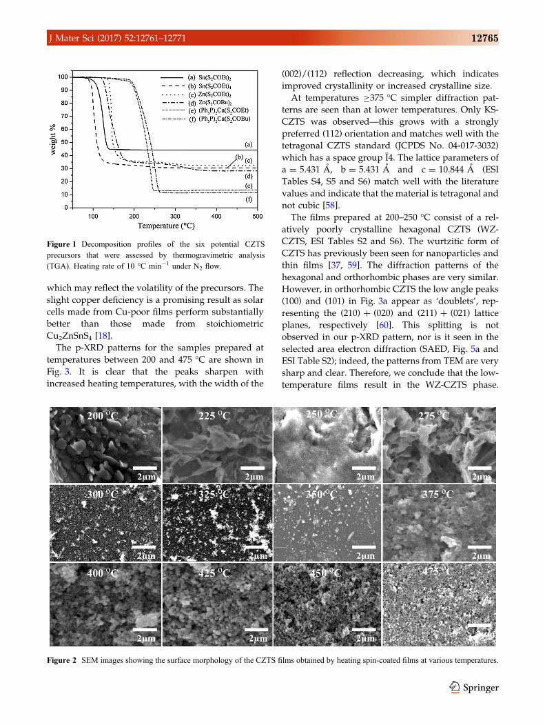
Thermogravimetric analysis (TGA, Fig. 1) demon-
strates the decomposition range of the Sn, Zn and Cu
xanthates in a nitrogen atmosphere. An optimum
mixture of precursors for melt reactions is one in
which the precursors all decompose at similar reac-
tion temperatures.
[Sn(S2COEt)2] decomposes cleanly in TGA at
100–145 �C, whereas [Zn(S2COnBu)2] decomposes via
a two-step process between 110–220 and 250–350 �C.The decomposition of [(Ph3P)2CuS2COEt] shows a
mass loss starting at about 140 �C and finishing at
260 �C. The TGA curves indicate that SnS and CuS
are formed cleanly, while ZnS contains impurities up
to 350 �C. Sn(S2COEt)4 and (Ph3P)2(Cu(S2COnBu)2
have hence been discounted as viable precursors
owing to their decomposition temperatures that dif-
fer from other precursors. The ethyl xanthate of zinc
[Zn(S2COEt)2] is much more hydroscopic than its
n-butyl cousin. Therefore, [(Ph3P)2CuS2COEt],
[Zn(S2COnBu)2] and [Sn(S2COEt)2] were chosen to
deposit CZTS films. Additionally, these complexes are
readily soluble in many common organic solvents.
CZTS thin films were prepared using a solution of
[(Ph3P)2CuS2COEt] (0.82 mmol), [Zn(S2COnBu)2]
(0.41 mmol) and [Sn(S2COEt)2] (0.41 mmol) dis-
solved in THF (6 ml) and spin coated onto a glass
slide. The resulting films were then heated in an N2
atmosphere at the desired temperature (between 200
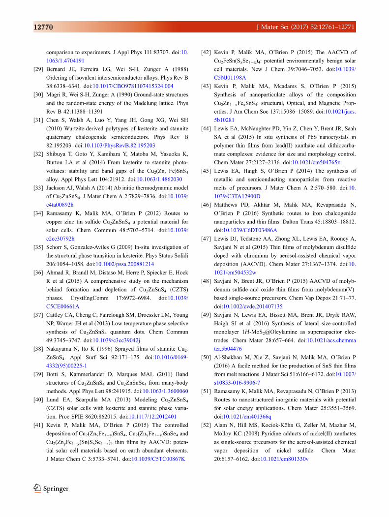
and 475 �C) for 120 min. The CZTS films were gray
for all of the heating temperatures. Scanning electron
microscopy (SEM) images (Fig. 2) reveal the surface
morphology of the films to be predominantly gran-
ular for the films prepared at temperatures[300 �C,with particles in the region of 0.25 lm in diameter.
The films prepared at lower temperature have a more
flake-like consistency and contain much smaller
particles. Side-on SEM images (ESI Figure S5) show
that the films are 1.85–2.0 lm in thickness.
Energy-dispersive X-ray spectroscopy (EDX) anal-
ysis shows the presence of copper, zinc, tin and sulfur
in the films. It is important to determine the Zn/Sn
and Cu/(Zn ? Sn) ratios within the films as slight
changes in these values can lead to significant chan-
ges in structural/electronic properties [57]. The EDX
measured compositions of the as-prepared films are
shown in ESI Table S1.
The Cu/(Zn ? Sn) ratio is in the range of 0.8–1.0
(ESI Table S1). The films heated at 225 �C gave Cu/
(Zn ? Sn)[ 1, whereas the other films heated at high
temperatures are copper deficient (ESI Table S1),
12764 J Mater Sci (2017) 52:12761–12771
which may reflect the volatility of the precursors. The
slight copper deficiency is a promising result as solar
cells made from Cu-poor films perform substantially
better than those made from stoichiometric
Cu2ZnSnS4 [18].
The p-XRD patterns for the samples prepared at
temperatures between 200 and 475 �C are shown in
Fig. 3. It is clear that the peaks sharpen with
increased heating temperatures, with the width of the
(002)/(112) reflection decreasing, which indicates
improved crystallinity or increased crystalline size.
At temperatures C375 �C simpler diffraction pat-
terns are seen than at lower temperatures. Only KS-
CZTS was observed—this grows with a strongly
preferred (112) orientation and matches well with the
tetragonal CZTS standard (JCPDS No. 04-017-3032)
which has a space group I4. The lattice parameters of
a = 5.431 A, b = 5.431 A and c = 10.844 A (ESI
Tables S4, S5 and S6) match well with the literature
values and indicate that the material is tetragonal and
not cubic [58].
The films prepared at 200–250 �C consist of a rel-
atively poorly crystalline hexagonal CZTS (WZ-
CZTS, ESI Tables S2 and S6). The wurtzitic form of
CZTS has previously been seen for nanoparticles and
thin films [37, 59]. The diffraction patterns of the
hexagonal and orthorhombic phases are very similar.
However, in orthorhombic CZTS the low angle peaks
(100) and (101) in Fig. 3a appear as ‘doublets’, rep-
resenting the (210) ? (020) and (211) ? (021) lattice
planes, respectively [60]. This splitting is not
observed in our p-XRD pattern, nor is it seen in the
selected area electron diffraction (SAED, Fig. 5a and
ESI Table S2); indeed, the patterns from TEM are very
sharp and clear. Therefore, we conclude that the low-
temperature films result in the WZ-CZTS phase.
Figure 1 Decomposition profiles of the six potential CZTS
precursors that were assessed by thermogravimetric analysis
(TGA). Heating rate of 10 �C min-1 under N2 flow.
Figure 2 SEM images showing the surface morphology of the CZTS films obtained by heating spin-coated films at various temperatures.
J Mater Sci (2017) 52:12761–12771 12765

Some contamination with binary or ternary phases
may occur, as can be observed in the films prepared at
\300 �C in which chalcocite (Cu2-xS) is identifiable
within the diffraction patterns.
The Raman spectra for the CZTS films give a good
indication of the phase formed (Fig. 3b). Kesteritic
CZTS has a relatively narrow and dominant Raman
shift at 338 cm-1 from the A1 mode, with further
peaks at 288 (A mode), 358 (B mode) and 372 cm-1 (B
mode) [61, 62]. This is seen in the films heated at
higher temperatures ([400 �C). For the samples pre-
pared at lower temperature (\300 �C), the major peak
has a shift of 327 cm-1 (ESI Figure S3). This corre-
sponds to the WZ-CZTS A mode [63]. This indicates
that the low-temperature films are wurtzite CZTS
and there is a phase transition to kesterite at higher
temperatures, in agreement with the p-XRD data. We
note that there is also a peak in the Raman spectra for
the 200 �C film at 468 cm-1, which corresponds to
Cu2S.
Increasing in temperature leads to a gradual nar-
rowing of the bands, and Raman bands appear with
frequencies of about 331, 333 and 337 cm-1. Films
heated at 475 �C showed a higher intensity band at
337 cm-1 (ESI Figure S4), which is indicative of KS–
CZTS [64].
Figure 4 shows the dependence of the shift of the
dominant Raman peak on the heating temperatures.
The WZ-CZTS films have a major peak at
326–327 cm-1, and this can clearly be seen for the
samples prepared at\350 �C. As the annealing tem-
perature increases, the peak moves toward 336 cm-1,
representing the presence of kesterite. This is
demonstrated by the rapid increase in Raman shift
seen from 375 to 475 �C. The p-XRD data show that
the films prepared at 400–450 �C are KS-CZTS too,
and the downshifted peak is due to disorder in Cu
and Zn atoms in the sublattice. This is because the Cu
and Zn atoms have a similar size and the difference
between binding energy of the cations in the sublat-
tice is small [65, 66].
Samples suitable for transmission electron micro-
scope (TEM) imaging were prepared by ultrasonica-
tion of the CZTS film (produced at 225, 350 and
450 �C, Fig. 5). Closer inspection of the CZTS pro-
duced at 225 �C found that two distinct kinds of
crystalline materials were present: a flake-like mate-
rial and short nanorods with lattices fringes present
(Fig. 5a). Both sets of crystals were typically\40 and
20 nm in diameter, respectively. We were able to
observe patches on the TEM grid that consisted
mainly of either phase. The selected area electron
diffraction (SAED) patterns found distinct rings—
indicative of polycrystalline materials, with these
rings consistent with the identification of hexagonal
(flake-like) and cubic (rod-like) phases of CZTS. This
SAED, inset to Fig. 5a, shows an interplanar spacing
of 0.27 and 0.19 nm, which correspond to the (200)
and (220) planes of cubic CZTS (ESI Table S3). The
interplanar spacing of 0.33 and 0.32 nm relates to the
(100) and (002) planes of hexagonal CZTS (ESI
Table S2). Two phases (hexagonal and cubic) can be
seen in the p-XRD pattern of the film heated at 225 �C(Fig. 3a) due to the equivalence of the (002) planes of
the hexagonal structure with the (111) planes of the
cubic structure.
Exfoliation of CZTS films produced at 350 �Cshowed a crystalline material (\20 nm); SAED sup-
ported the formation of only the tetragonal phase of
kesterite CZTS (Fig. 5b). The interplanar spacing of
0.31, 0.19 and 0.16 nm corresponds to the (112),
{(204)(220)} and {(312)(116)} planes of kesterite CZTS
(ESI Table S4). Likewise, for the film heated to 450 �C,we only observed crystalline particles \20 nm, and
for which the SAED could also be indexed to
tetragonal kesterite CZTS (Fig. 5c, ESI Table S5).
The electrical parameters of the WZ-CZTS film
prepared at 225 �C (ESI S6) and the phase pure KS-
CZTS samples annealed at 375 �C (ESI S7) and 450 �C(ESI S8) were obtained using the van der Pauw four-
probe configuration in Hall effect measurements at
room temperature. All samples exhibited p-type
conductivity, a desirable requirement for the fabri-
cation of heterojunction solar cells.
Table 1 Electrical properties of CZTS films prepared through
melt reactions at 375 and 450 �C
T 225 �C 375 �C 450 �C
l (cm2 v-1 s-1) 87.1 5.58 11.1
p (cm-3) 2.65 9 10?15 1.32 9 10?18 4.55 9 10?17
RH (C-1 cm3) 2.36 9 10?3 4.73 13.7
q (X cm) 27.1 0.85 1.23
r (S cm-1) 0.0369 1.18 0.81
RS (X/h) 1.37 9 10?5 4.35 9 10?3 6.55 9 10?3
Conductivity p-type p-type p-type
T annealing temperature, l Hall mobility, p Hall carrier density,
RH Hall coefficient, q resistivity, r conductivity and RS sheet
resistance
12766 J Mater Sci (2017) 52:12761–12771

The resistivity (q), Hall mobility (l), carrier con-
centration (p) and Hall coefficient (RH) are shown in
Table 1. The resistivity (q) decreased from 27.1 X cm
to around 1.23 X cm for the transition from WZ-
CZTS to KS-CZTS. In addition, we found that the
Hall coefficient (RH) decreased from
2.36 9 10?3 cm3 C-1 for WZ-CZTS films to
13.7 cm3 C-1 for KS-CZTS �C. We have determined
that for the two phases, the Hall mobility (l) is 87.1
and 11.1 cm2 V-1 s-1, respectively. The carrier con-
centration values were 2.65 9 10?15 and
4.55 9 10?17 cm-3, the latter of which is an excellent
value for use in practical devices.
TEM images of the film prepared at 225 �C indicate
that the film exhibited hexagonal CZTS as well as
cubic (Fig. 5a). This confirms the presence of impu-
rities in the predominantly wurtzite phase CZTS.
McGill [67] and Hall [68] previously showed that as
the impurity concentration increases, the mobility
decreases. This behavior has also been seen for Si [69]
and GaAs [70]. This model can be applied to the
CZTS system, as moving from 225 to 375/450 �C we
see a substantial decrease in mobility.
Conclusions
Thermogravimetric analysis was used to investigate
the decomposition of a series of O-n-butyl and O-
ethylxanthate complexes of copper, tin and zinc.
[(Ph3P)2CuS2COEt], [Zn(S2COnBu)2] and [Sn(S2COEt)2]
were found to have compatible decomposition tem-
peratures and were used for the formation of
Figure 3 a p-XRD patterns and b Raman scattering spectra of
CZTS thin films annealed in an N2 atmosphere at the desired
temperature (200–475 �C) for 120 min. Chalcocite (Cu2-xS) is
identifiable within the p-XRD for temperatures \300 �C: low-
intensity peaks for the (110) plane (2h = 46.7�) and (103) plane
(2h = 48.8�).
Figure 4 The position of the dominant Raman peak at
326–336 cm-1 in Fig. 3b and its relationship to the annealing
temperature of the films.
J Mater Sci (2017) 52:12761–12771 12767

Cu2ZnSnS4 (CZTS) by spin coating followed by
heating under N2. The p-XRD patterns of CZTS thin
films were obtained after heating at temperatures
between 200 and 475 �C and revealed a temperature
dependence of the CZTS phase formed. Higher
temperatures give the normal tetragonal phase CZTS,
while low temperatures are mixed hexagonal and
cubic phases. EDX measurements show that the Cu/
(Zn ? Sn) ratio was between 1 and 0.64. The mea-
sured resistivity, carrier concentration, mobility and
Hall coefficient of films heated at 225, 375 and 450 �C,indicated fairly homogenous films. In this work the
wurtzite CZTS has a much higher resistivity and
mobility, but a much lower charge carrier density.
Acknowledgements
The authors would like to acknowledge the Iraqi
Culture Attache in London for financial support
(M.A.S.) and the EPSRC (Doctoral Prize for P.D.M.,
EP/M507969/1). N.S. thanks Carl and Anne Parker
for the fellowship that funded this work. Some of the
equipment used in this study were provided by the
Engineering and Physical Sciences Research Council
(Core Capability in Chemistry, EPSRC Grant Number
EP/K039547/1).
Open Access This article is distributed under the
terms of the Creative Commons Attribution 4.0
International License (http://creativecommons.org/
licenses/by/4.0/), which permits unrestricted use,
distribution, and reproduction in any medium, pro-
vided you give appropriate credit to the original
author(s) and the source, provide a link to the Crea-
tive Commons license, and indicate if changes were
made.
Electronic supplementary material: The online
version of this article (doi:10.1007/s10853-017-1367-0)
contains supplementary material, which is available to
authorized users.
References
[1] Woo K, Kim Y, Moon J (2012) A non-toxic, solution-pro-
cessed, earth abundant absorbing layer for thin-film solar
cells. Energy Environ Sci 5:5340–5345. doi:10.1039/
c1ee02314d
[2] Katagiri H, Jimbo K, Maw WS, Oishi K, Yamazaki M, Araki
H et al (2009) Development of CZTS-based thin film solar
cells. Thin Solid Films 517:2455–2460. doi:10.1016/j.tsf.
2008.11.002
[3] Matthews PD, McNaughter PD, Lewis DJ, O’Brien P (2017)
Shining a light on transition metal chalcogenides for sus-
tainable photovoltaics. Chem Sci 8:4177–4187. doi:10.1039/
C7SC00642J
[4] Shin B, Gunawan O, Zhu Y, Bojarczuk NA, Chey SJ, Guha
S (2013) Thin film solar cell with 8.4% power conversion
efficiency using an earth-abundant Cu2ZnSnS4 absorber.
Prog Photovolt Res Appl 21:72–76. doi:10.1002/pip.1174
Figure 5 TEM images of Cu2ZnSnS4 nanocrystals. a A CZTS
film heated at 225 �C. The insets show selected area electron
diffraction (SAED) images, gray box for cubic CZTS and white
box for hexagonal CZTS. b A film heated at 350 �C. The SAED
pattern can be indexed to tetragonal CZTS. c A film heated at
450 �C, the inset SAED pattern is also indexed to tetragonal
CZTS.
12768 J Mater Sci (2017) 52:12761–12771

[5] Saha SK, Guchhait A, Pal AJ (2012) Cu2ZnSnS4 (CZTS)
nanoparticle based nontoxic and earth-abundant hybrid pn-
junction solar cells. Phys Chem Chem Phys 14:8090–8096.
doi:10.1039/c2cp41062a
[6] Scragg JJ, Dale PJ, Peter LM, Zoppi G, Forbes I (2008) New
routes to sustainable photovoltaics: evaluation of Cu2ZnSnS4as an alternative absorber material. Phys Status Solidi
245:1772–1778. doi:10.1002/pssb.200879539
[7] Jimbo K, Kimura R, Kamimura T, Yamada S, Maw WS,
Araki H et al (2007) Cu2ZnSnS4-type thin film solar cells
using abundant materials. Thin Solid Films 515:5997–5999.
doi:10.1016/j.tsf.2006.12.103
[8] Ito K, Nakazawa T (1988) Electrical and optical properties of
stannite-type quaternary semiconductor thin films. Jpn J
Appl Phys 27:2094–2097. doi:10.1143/JJAP.27.2094
[9] Katagiri H, Sasaguchi N, Hando S, Hoshino S, Ohashi J,
Yokota T (1997) Preparation and evaluation of Cu2ZnSnS4thin films by sulfurization of E-B evaporated precursors. Sol
Energy Mater Sol Cells 49:407–414. doi:10.1016/S0927-
0248(97)00119-0
[10] Shin SW, Pawar SM, Park CY, Yun JH, Moon JH, Kim JH
et al (2011) Studies on Cu2ZnSnS4 (CZTS) absorber layer
using different stacking orders in precursor thin films. Sol
Energy Mater Sol Cells 95:3202–3206. doi:10.1016/j.sol
mat.2011.07.005
[11] Suryawanshi MP, Agawane GL, Bhosale SM, Shin SW, Patil
PS, Kim JH et al (2013) CZTS based thin film solar cells: a
status review. Mater Technol 28:98–109. doi:10.1179/
1753555712y.0000000038
[12] Kumar M, Dubey A, Adhikari N, Venkatesan S, Qiao Q
(2015) Strategic review of secondary phases, defects and
defect-complexes in kesterite CZTS–Se solar cells. Energy
Environ Sci 8:3134–3159. doi:10.1039/C5EE02153G
[13] Ramasamy K, Malik MA, O’Brien P (2011) The chemical
vapor deposition of Cu2ZnSnS4 thin films. Chem Sci
2:1170–1172. doi:10.1039/c0sc00538j
[14] Schurr R, Holzing A, Jost S, Hock R, Voss T, Schulze J et al
(2009) The crystallisation of Cu2ZnSnS4 thin film solar cell
absorbers from co-electroplated Cu-Zn-Sn precursors. Thin
Solid Films 517:2465–2468. doi:10.1016/j.tsf.2008.11.019
[15] Wangperawong A, King JS, Herron SM, Tran BP, Pangan-
Okimoto K, Bent SF (2011) Aqueous bath process for
deposition of Cu2ZnSnS4 photovoltaic absorbers. Thin Solid
Films 519:2488–2492. doi:10.1016/j.tsf.2010.11.040
[16] Su Z, Yan C, Sun K, Han Z, Liu F, Liu J et al (2012)
Preparation of Cu2ZnSnS4 thin films by sulfurizing stacked
precursor thin films via successive ionic layer adsorption and
reaction method. Appl Surf Sci 258:7678–7682. doi:10.
1016/j.apsusc.2012.04.120
[17] Chen LJ, Chuang YJ (2013) Quaternary semiconductor
derived and formation mechanism by non-vacuum route
from solvothermal nanostructures for high-performance
application. Mater Lett 91:372–375. doi:10.1016/j.matlet.
2012.10.037
[18] Johnson MC, Wrasman C, Zhang X, Manno M, Leighton C,
Aydil ES (2015) Self-regulation of Cu/Sn ratio in the syn-
thesis of Cu2ZnSnS4 films. Chem Mater 27:2507–2514.
doi:10.1021/acs.chemmater.5b00108
[19] Feng Y, Yu B, Cheng G, Lau T, Li Z, Yin L et al (2015)
Searching for a fabrication route of efficient Cu2ZnSnS4solar cells by post-sulfuration of co-sputtered Sn-enriched
precursors. J Mater Chem C 3:9650–9656. doi:10.1039/
C5TC02486B
[20] Scragg JJ, Ericson T, Kubart T, Edo M, Platzer-Bjorkman C
(2011) Chemical insights into the instability of Cu2ZnSnS4Films during annealing. Chem Mater 23:4625–4633. doi:10.
1021/cm202379s
[21] Yu K, Carter EA (2015) A strategy to stabilize kesterite
CZTS for high-performance solar cells. Chem Mater
27:2920–2927. doi:10.1021/acs.chemmater.5b00172
[22] Yu K, Carter EA (2016) Determining and controlling the
stoichiometry of Cu2ZnSnS4 photovoltaics: the physics and
its implications. Chem Mater 28:4415–4420. doi:10.1021/
acs.chemmater.6b01612
[23] Scragg JJ, Kubart T, Watjen JT, Ericson T, Linnarsson MK,
Platzer-Bjorkman C (2013) Effects of back contact insta-
bility on Cu2ZnSnS4 devices and processes. Chem Mater
25:3162–3171. doi:10.1021/cm4015223
[24] Jiang F, Gunawan T, Harada Y, Kuang T, Minegishi K
Domen et al (2015) Pt/In2S3/CdS/Cu2ZnSnS4 thin film as an
efficient and stable photocathode for water reduction under
sunlight radiation. J Am Chem Soc 137:13691–13697.
doi:10.1021/jacs.5b09015
[25] Chang J, Waclawik ER (2014) Colloidal semiconductor
nanocrystals: controlled synthesis and surface chemistry in
organic media. RSC Adv 4:23505–23527. doi:10.1039/
c4ra02684e
[26] Chen S, Gong XG, Walsh A, Wei SH (2009) Crystal and
electronic band structure of Cu2ZnSnX4 (X = S and Se)
photovoltaic absorbers: first-principles insights. Appl Phys
Lett 94:25–27. doi:10.1063/1.3074499
[27] Paier J, Asahi R, Nagoya A, Kresse G (2009) Cu2ZnSnS4 as
a potential photovoltaic material: a hybrid Hartree-Fock
density functional theory study. Phys Rev B 79:115126.
doi:10.1103/PhysRevB.79.115126
[28] Khare A, Himmetoglu B, Johnson M, Norris DJ, Cococcioni
M, Aydil ES (2012) Calculation of the lattice dynamics and
Raman spectra of copper zinc tin chalcogenides and
J Mater Sci (2017) 52:12761–12771 12769
comparison to experiments. J Appl Phys 111:83707. doi:10.
1063/1.4704191
[29] Bernard JE, Ferreira LG, Wei S-H, Zunger A (1988)
Ordering of isovalent intersemiconductor alloys. Phys Rev B
38:6338–6341. doi:10.1017/CBO9781107415324.004
[30] Magri R, Wei S-H, Zunger A (1990) Ground-state structures
and the random-state energy of the Madelung lattice. Phys
Rev B 42:11388–11391
[31] Chen S, Walsh A, Luo Y, Yang JH, Gong XG, Wei SH
(2010) Wurtzite-derived polytypes of kesterite and stannite
quaternary chalcogenide semiconductors. Phys Rev B
82:195203. doi:10.1103/PhysRevB.82.195203
[32] Shibuya T, Goto Y, Kamihara Y, Matoba M, Yasuoka K,
Burton LA et al (2014) From kesterite to stannite photo-
voltaics: stability and band gaps of the Cu2(Zn, Fe)SnS4alloy. Appl Phys Lett 104:21912. doi:10.1063/1.4862030
[33] Jackson AJ, Walsh A (2014) Ab initio thermodynamic model
of Cu2ZnSnS4. J Mater Chem A 2:7829–7836. doi:10.1039/
c4ta00892h
[34] Ramasamy K, Malik MA, O’Brien P (2012) Routes to
copper zinc tin sulfide Cu2ZnSnS4 a potential material for
solar cells. Chem Commun 48:5703–5714. doi:10.1039/
c2cc30792h
[35] Schorr S, Gonzalez-Aviles G (2009) In-situ investigation of
the structural phase transition in kesterite. Phys Status Solidi
206:1054–1058. doi:10.1002/pssa.200881214
[36] Ahmad R, Brandl M, Distaso M, Herre P, Spiecker E, Hock
R et al (2015) A comprehensive study on the mechanism
behind formation and depletion of Cu2ZnSnS4 (CZTS)
phases. CrystEngComm 17:6972–6984. doi:10.1039/
C5CE00661A
[37] Cattley CA, Cheng C, Fairclough SM, Droessler LM, Young
NP, Warner JH et al (2013) Low temperature phase selective
synthesis of Cu2ZnSnS4 quantum dots. Chem Commun
49:3745–3747. doi:10.1039/c3cc39042j
[38] Nakayama N, Ito K (1996) Sprayed films of stannite Cu2-ZnSnS4. Appl Surf Sci 92:171–175. doi:10.1016/0169-
4332(95)00225-1
[39] Botti S, Kammerlander D, Marques MAL (2011) Band
structures of Cu2ZnSnS4 and Cu2ZnSnSe4 from many-body
methods. Appl Phys Lett 98:241915. doi:10.1063/1.3600060
[40] Lund EA, Scarpulla MA (2013) Modeling Cu2ZnSnS4(CZTS) solar cells with kesterite and stannite phase varia-
tion. Proc SPIE 8620:862015. doi:10.1117/12.2012401
[41] Kevin P, Malik MA, O’Brien P (2015) The controlled
deposition of Cu2(ZnyFe1-y)SnS4, Cu2(ZnyFe1-y)SnSe4 and
Cu2(ZnyFe1-y)Sn(SxSe1-x)4 thin films by AACVD: poten-
tial solar cell materials based on earth abundant elements.
J Mater Chem C 3:5733–5741. doi:10.1039/C5TC00867K
[42] Kevin P, Malik MA, O’Brien P (2015) The AACVD of
Cu2FeSn(SxSe1-x)4: potential environmentally benign solar
cell materials. New J Chem 39:7046–7053. doi:10.1039/
C5NJ01198A
[43] Kevin P, Malik MA, Mcadams S, O’Brien P (2015)
Synthesis of nanoparticulate alloys of the composition
Cu2Zn1-xFexSnS4: structural, Optical, and Magnetic Prop-
erties. J Am Chem Soc 137:15086–15089. doi:10.1021/jacs.
5b10281
[44] Lewis EA, McNaughter PD, Yin Z, Chen Y, Brent JR, Saah
SA et al (2015) In situ synthesis of PbS nanocrystals in
polymer thin films from lead(II) xanthate and dithiocarba-
mate complexes: evidence for size and morphology control.
Chem Mater 27:2127–2136. doi:10.1021/cm504765z
[45] Lewis EA, Haigh S, O’Brien P (2014) The synthesis of
metallic and semiconducting nanoparticles from reactive
melts of precursors. J Mater Chem A 2:570–580. doi:10.
1039/C3TA12900D
[46] Matthews PD, Akhtar M, Malik MA, Revaprasadu N,
O’Brien P (2016) Synthetic routes to iron chalcogenide
nanoparticles and thin films. Dalton Trans 45:18803–18812.
doi:10.1039/C6DT03486A
[47] Lewis DJ, Tedstone AA, Zhong XL, Lewis EA, Rooney A,
Savjani N et al (2015) Thin films of molybdenum disulfide
doped with chromium by aerosol-assisted chemical vapor
deposition (AACVD). Chem Mater 27:1367–1374. doi:10.
1021/cm504532w
[48] Savjani N, Brent JR, O’Brien P (2015) AACVD of molyb-
denum sulfide and oxide thin films from molybdenum(V)-
based single-source precursors. Chem Vap Depos 21:71–77.
doi:10.1002/cvde.201407135
[49] Savjani N, Lewis EA, Bissett MA, Brent JR, Dryfe RAW,
Haigh SJ et al (2016) Synthesis of lateral size-controlled
monolayer 1H-MoS2@Oleylamine as supercapacitor elec-
trodes. Chem Mater 28:657–664. doi:10.1021/acs.chemma
ter.5b04476
[50] Al-Shakban M, Xie Z, Savjani N, Malik MA, O’Brien P
(2016) A facile method for the production of SnS thin films
from melt reactions. J Mater Sci 51:6166–6172. doi:10.1007/
s10853-016-9906-7
[51] Ramasamy K, Malik MA, Revaprasadu N, O’Brien P (2013)
Routes to nanostructured inorganic materials with potential
for solar energy applications. Chem Mater 25:3551–3569.
doi:10.1021/cm401366q
[52] Alam N, Hill MS, Kociok-Kohn G, Zeller M, Mazhar M,
Molloy KC (2008) Pyridine adducts of nickel(II) xanthates
as single-source precursors for the aerosol-assisted chemical
vapor deposition of nickel sulfide. Chem Mater
20:6157–6162. doi:10.1021/cm801330v
12770 J Mater Sci (2017) 52:12761–12771
[53] Kociok-Kohn G, Molloy KC, Sudlow AL (2014) Molecular
routes to Cu2ZnSnS4: a comparison of approaches to bulk
and thin-film materials. Can J Chem 92:514–524. doi:10.
1139/cjc-2013-0497
[54] van der Pauw LJ (1958) A method of measuring specific
resistivity and hall effect of discs of arbitrary shape. Philips
Res Rep 13:1–9. doi:10.1017/CBO9781107415324.004
[55] Mohamed AA, Kani I, Ramirez AO, Fackler JP (2004)
Synthesis, characterization, and luminescent properties of
Dinuclear Gold(I) Xanthate complexes: X-ray structure of
[Au2(nBu-xanthate)2]. Inorg Chem 43:3833–3839. doi:10.
1021/ic0349858
[56] Raston CL, Tennant PR, White AH, Winter G (1978)
Reactions of tin(II) and tin(IV) xanthates: crystal structure of
Tetrakis (O-ethylxanthato) tin(IV). Aust J Chem
31:1493–1500. doi:10.1071/CH9781493
[57] Zhou S, Tan R, Jiang X, Shen X, Xu W, Song W (2013)
Growth of CZTS thin films by sulfurization of sputtered
single-layered Cu-Zn-Sn metallic precursors from an alloy
target. J Mater Sci Mater Electron 24:4958–4963. doi:10.
1007/s10854-013-1507-5
[58] Bonazzi P, Bindi L, Bernardini GP, Menchetti S (2003) A
model for the mechanism of incorporation of Cu, Fe, and Zn
in the Stannite–Kesterite series, Cu2FeSnS4–Cu2ZnSnS4.
Can Mineralogist 41:639–647. doi:10.2113/gscanmin.41.3.
639
[59] Mainz R, Singh A, Levcenko S, Klaus M, Genzel C, Ryan
KM et al (2014) Phase-transition-driven growth of com-
pound semiconductor crystals from ordered
metastable nanorods. Nat Commun 5:3133. doi:10.1038/
ncomms4133
[60] Jiang H, Dai P, Feng Z, Fan W, Zhan J (2012) Phase
selective synthesis of metastable orthorhombic Cu2ZnSnS4.
J Mater Chem 22:7502–7506. doi:10.1039/c2jm16870g
[61] Cheng A-J, Manno M, Khare A, Leighton C, Campbell SA,
Aydil ES (2011) Imaging and phase identification of
Cu2ZnSnS4 thin films using confocal Raman spectroscopy.
J Vac Sci Technol A 29:51203. doi:10.1116/1.3625249
[62] Dimitrievska M, Fairbrother A, Fontane X, Jawhari T,
Izquierdo-Roca V, Saucedo E et al (2014) Multiwavelength
excitation Raman scattering study of polycrystalline kesterite
Cu2ZnSnS4 thin films. Appl Phys Lett 104:21901. doi:10.
1063/1.4861593
[63] Tan JMR, Lee YH, Pedireddy S, Baikie T, Ling XY, Wong
LH (2014) Understanding the synthetic pathway of single
phase quarternary semiconductor using surface-enhanced
Raman scattering: a case of Wurtzite Cu2ZnSnS4 nanopar-
ticles. J Am Chem Soc 136:6684–6692. doi:10.1021/
ja501786s
[64] Himmrich M, Haeuseler H (1991) Far infrared studies on
stannite and wurtzstannite type compounds. Spectrochim
Acta 47A:933–942. doi:10.1016/0584-8539(91)80283-O
[65] Valakh MY, Kolomys OF, Ponomaryov SS, Yukhymchuk
VO, Babichuk IS, Izquierdo-Roca V et al (2013) Raman
scattering and disorder effect in Cu2ZnSnS4. Phys Status
Solidi Rapid Res Lett 7:258–261. doi:10.1002/pssr.
201307073
[66] Walsh A, Chen S, Wei SH, Gong XG (2012) Kesterite thin-
film solar cells: advances in materials modelling of
Cu2ZnSnS4. Adv Energy Mater 2:400–409. doi:10.1002/
aenm.201100630
[67] McGill TC, Baron R (1975) Neutral impurity scattering in
semiconductors. Phys Rev B 11:5208–5210
[68] Hall GL (1962) Ionized impurity scattering in semiconduc-
tors. J Phys Chem Solids 23:1147–1151. doi:10.1103/Phys
RevB.20.3254
[69] Kosina H, Kaiblinger-Grujin G (1998) Ionized-impurity
scattering of majority electrons in silicon. Solid State Elec-
tron 42:331–338. doi:10.1016/S0038-1101(97)00199-8
[70] Wolfe CM, Stillman GE, Dimmock JO (1970) Ionized
impurity density in n-type GaAs. J Appl Phys 41:504–507.
doi:10.1063/1.1658704
J Mater Sci (2017) 52:12761–12771 12771