The Super Doubler Group 31 - UCF Department of EECS · The Super Doubler Group 31 ... •...
55
The Super Doubler Group 31 Kenneth Richardson BSCpE Gilson Rodrigues BSEE John Shepherd BSEE Stephen Williams BSEE
Transcript of The Super Doubler Group 31 - UCF Department of EECS · The Super Doubler Group 31 ... •...

The Super DoublerGroup 31
Kenneth Richardson BSCpE
Gilson Rodrigues BSEE
John Shepherd BSEE
Stephen Williams BSEE

Motivation
Analog video (240p) processed by a digital TV
• Digital TVs have limited analog video support• Typically only support composite video• Situation will worsen with time
Analog video (240p) on a digital TV with a video pre-processor

Video System Compatibility
• Using RGB video output via SCART offers large improvement over composite video
• Need device to bridge the gap between analog SCART and digital HDMI
SCART

XRGB mini- Framemeister
Flaws of the Framemeister• No dedicated line double mode• Results in higher latency• 240p <-> 480i mode switch time• $340 shipped
Features of the Framemeister• Improved 240p handling• Supports SCART• Fine grain control of image settings

The Super Doubler
• Low cost high-speed scaling device
• Versatile input selection
• Digital video via HDMI output
• Fills gap between cheap scalers and Framemeister
• System firmware can be updated with reprogramming options
Requirements
Scaling factor ≥ 2
BOM ≤ $150
FPGA block latency < 28ms
240p <-> 480i mode switch < 33ms
Supported input: VGA, SCART, component, s-video

System Block Diagram

Input Signals
SCART (RGB)
COMPONENT(YPbPr)
VGA
S-VIDEO
• Wide input selection
• Support most common retro consoles
• SEGA Genesis – SCART
• SEGA Dreamcast – VGA
• Nintendo 64 – S-Video
• etc…

Input Video Filtering
THS7353 Low pass filter
Device Control Method I2C (Individually configurable)
Number of channels 3
Gain(dB) Adjustable
Size 4.4 x 6.5 ~ 42 𝑚𝑚2
Price $1.49Texas Instruments - THS7353
• 2 3-Channel Input Low Power Video Amp with I2C Control
• Channels individually configurable
• 5th Order Butterworth Characteristics
• Configurable cutoff frequency

THS7353 – Schematic
Component
SCART/VGA

ADV7181D - Video Decoder
ADV7181
Family Interface - Encoders, Decoders, Converters
Cost $12.51
Category Integrated Circuits (ICs)
Voltage - Supply, Analog 3.15 V ~ 3.45 V
Voltage - Supply, Digital 1.65 V ~ 2 V
Package / Case 64-LFCSP (9mm x 9mm)ADV7181 Video decoder
• Detects and converts analog video signals to digital format
• Compatibility with various video standards – NTSC, PAL and SECAM
• Six analog video input channels
• Accepts: SCART (RGB), Component (YPbPr), S-Video and VGA video signals
• Video decoding and conversion in line-locked clock-based systems

ADV7181 – Inputs
SCART/VGA
COMPONENT
S-VIDEO

Scan type - Interlaced

Scan type - Progressive
• Single field contains the entire frame
• 1 Field = 1 Frame
• New “Fixed resolution” displays (such as LCD, LED) all use progressive scan.

Interlaced versus Progressive

FPGA Video Processing Unit
• Xilinx Artix-7 FPGA Family• Low-cost FPGA giving access to latest tools
• Wide range of devices to choose from
• Verilog HDL
• Vivado Design software
• Performs video scaling
FPGA Family Artix-7
Cost $32.13 - $251.25
FPGA Package Various BGA
Logic Slices 2,600 - 33,650
Block Memory 900Kb – 13.14Mb
PLL 5 - 10

Nexys Video FPGA Development Board
FPGA Artix-7 XC7A200T
Cost $320
Size 5.25in x 5.50in
FPGA Package 484-BBGA
Logic Slices 33,650
Block Memory 13 Mbits
PLL 10
• HDMI Output (1080p capable)• “Bare metal” HDMI pin access• Large number of high-speed I/O• LPC FPGA Mezzanine Connector (FMC)

FPGA Block Diagram
ADV7181DDecoder output
HDMI Connector Pins

Video Formatting
• FPGA receives video data in 12-bit RGB DDR format• FPGA needs to reorder data before scaling

Video Formatting
1 Byte of Red Pixel Data 1 Byte of Green Pixel Data 1 Byte of Blue Pixel Data
12-bit DDR RGB Pixel Data up to 75MHz

Scaling Method
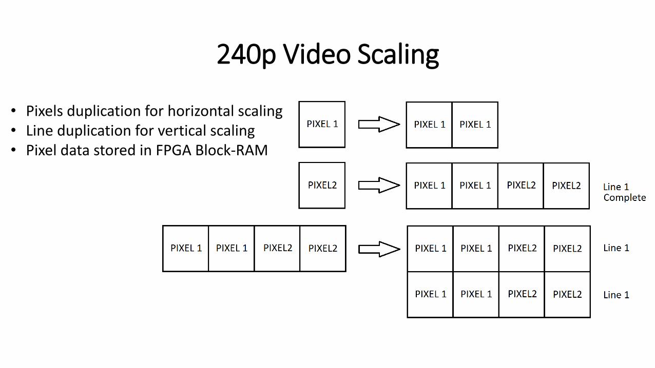
240p Video Scaling
• Pixels duplication for horizontal scaling• Line duplication for vertical scaling• Pixel data stored in FPGA Block-RAM

HDMI Output
• HDMI uses 8 FPGA I/O versus 26 for VGA• Reduces PCB complexity
• Single Cable for both audio and video
• HDMI signal encoding performed in FPGA logic• Reduces BOM and PCB complexity
SupportedVideo Modes
640x480p 60Hz
960x720p 60Hz
1280x960p 60Hz
Scale 2x
Scale 3x
Scale 4x

MCU Integration
Key Responsibilities
• Initialization of video buffer ICs, video decoder (I2C)
• Handling user IR control requests
• File IO for settings save/load
• Reconfiguring input stage ICs per user requests
• On-device feedback via LEDs
• FPGA video processing real time control

Microcontroller Comparison
Device MSP430 TM4C123 STM32F030 STM32F070 STM32F103
Clock 16 MHz 80 MHz 48 MHz 48 MHz 72 MHz
Bus Width 16 bits 32 bit 32 bit 32 bit 32 bit
Package Various LQFP64 LQFP64 LQFP64 LQFP64
Code Mem 16 kB 256 kB 64 kB 128 kB 128 kB
Data Mem 512 B 32 kB 8 kB 16 kB 20 kB
I/O Pins Up to 24 Up to 43 55 51 51
Timers 2 12+ 7 7 7
Price $2.80 $11.00 $2.11 $4.70 $7.14
• MSP430 considered for low cost and prior familiarity
• TM4C123 offers TI ecosystem and tools in a Cortex M4 design
• Several STMicro offerings, all ARM (F0 Cortex M0 and F1 Cortex M3

STM32F070RBT6
• Significant performance gain over MSP430
• Middle-ground in cost-performance
• Extensive peripheral support
• Up to 51 GPIOs
• 2 I2C hardware interfaces
• 4 USART hardware interfaces
• 2 SPI blocks
• SWD (Serial Wire Debug) ready via ST-LinkV2
• ST factory bootloader for program flashing over UART (enabled via
single pin jumper configuration)
• Nucleo development boards
12mm x 12 mm

STM32 Development Tools
Nucleo Development Boards
• Full pin breakout from the LQFP64 package
• STLinkV2 emulation for SWD access
• Extremely low cost, typically < $10
• Available with our specific F070RBT6 MCU
Keil MDK and uVision IDE
• Professional development platform
• Compiler toolchain and RTOS kernel
• Large code size license (256k) for use with
STM32 Cortex M0 devices

Reprogramming Options
Serial Wire Debug
• ARM standard programming and debugging interface
• ST provides interface via ST-LinkV2
• Small board footprint, only 5 pins required
• Adapter via Adafruit at right ($12.50), similar can be
had for ~$5 on ebay
• Nucleo boards can also be configured as programmers
ST Bootloader
• Factory programmed boot option for STM32 devices
• Allows flashing chip via UART interface, no debug
• ST provided Flash Loader Demonstrator application

Microcontroller Interfaces
MCU chief responsibilities are system
initialization, integration, and interface control
• GPIOs
• IR receiver, LEDs, FPGA
• I2C bus
• Video decoder, video buffers
• SPI
• uSD in SPI mode
• Reprogramming interfaces
• SWD, UART-USB via FT232

USB-UART IC (FT232RL)
• Translation from USB <-> UART
• Built in regulator to (optionally) convert logic
levels from 5V to 3.3V. Configurable to other
logic levels
• Used in previous projects and breakouts on
hand
• Small board footprint, approx. 10x8 mm in
SSOP-28 package (shown right)
• ~$4.50

MCU Peripheral Board (Schematic)

System Initialization
• Settings load from uSD
• Input select for video buffers, signal
format select and other settings for
video decoder (> 100 registers)
• Initialize MCU internal peripherals for
IR/Interrupts
• Start main control loop
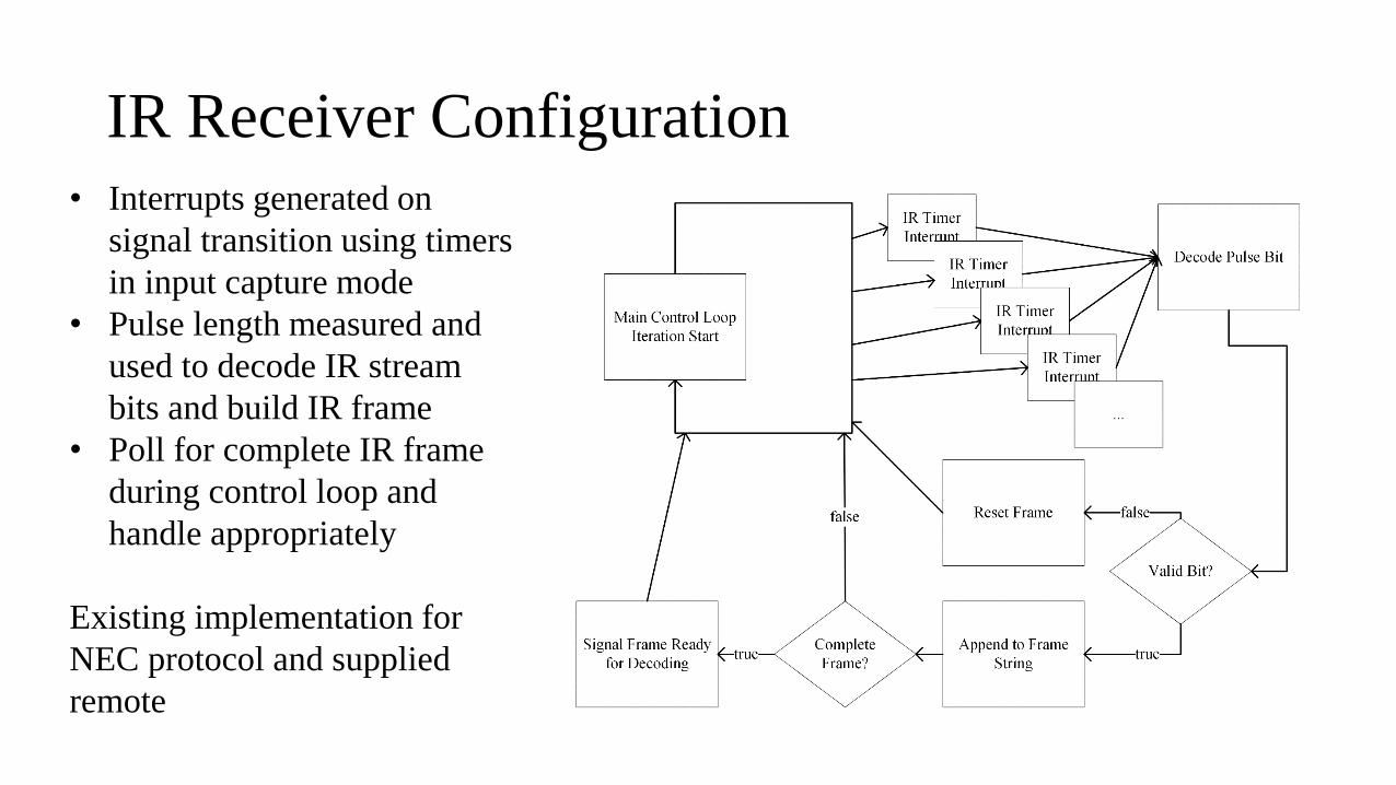
IR Receiver Configuration• Interrupts generated on
signal transition using timers
in input capture mode
• Pulse length measured and
used to decode IR stream
bits and build IR frame
• Poll for complete IR frame
during control loop and
handle appropriately
Existing implementation for
NEC protocol and supplied
remote

Remote Control Interface
Supported Controls:
• Freeze Frame
• Brightness Adjustment
• Contrast Adjustment
• Save Brightness/Contrast to uSD
• Load Brightness/Contrast from uSD
• Reload Default Brightness/Contrast
• Input Selection
• Toggle Scanline Emulation
• Refresh FPGA Sync

Control Summary
• Basic Control Loop
• Check for user input
• Update devices accordingly
• Update relevant status data
from special purpose ICs
• Update output
• LEDs
• Yellow – Decoder detected
• Red – FPGA held in reset

Library Support
STM32 Standard Peripheral Library
• Register configuration abstraction for peripherals (I2C, SPI, Timers, etc)
• Not particularly well documented, existing examples and ecosystems focus
on F1 and F4 (Cortex M3 and M4 respectively) devices with different
implementation
STM32 EVAL Examples
• Example implementations of extended functionality using STM32 devices
• e.g. infrared receiver
• Application notes/guidance on modifying for general purpose

Library Support
FatFS
• FAT implementation for embedded devices
• Provides filesystem abstraction for user application with a
handful of user implemented device interface functions
• disk_status()
• disk_initialize()
• disk_read()
• disk_write()
• disk_ioctl()
• get_fattime()
• Interface provided to uSD via SPI interface

Device Prototyping
• Initially designed system to incorporate MCU, input buffers, and video decoder
on a single PCB
• PCBs prototyped as standalone boards for testing before expected integration
• Three PCBs for testing each major component
• Video Decoder
• MCU
• Video Filter

Analog Video Input PCB
• Front • Back


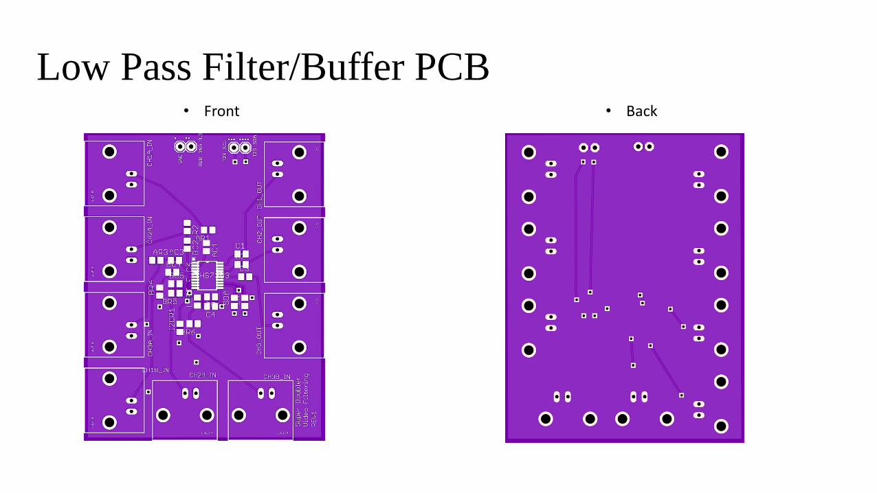
Low Pass Filter/Buffer PCB• Front • Back

MCU Peripheral Board (Layout)

Board Manufacturing/Assembly
• All boards ordered via OSH Park
• Non hand-solderable components mounted by Quality Manufacturing Services
thanks to Sam Hanna
• ICs, uSD socket, USB socket
• All other components populated using group owned equipment

Challenges
• Significant issues with group-designed video decoder PCB
• Board could not support the required settings for our operation mode
(RGB DDR using component processor)
• One setting using standard definition processor worked, but gave erratic
behavior
• Decoder output pixel clock performing nothing like expected behavior,
extreme effort to modify configuration to produce expected output
resulted in no improvements even over new board revisions

Challenges
Example output from Decoder
board Pixel Clock
• Should be a consistent 13.5
MHz roughly square wave
• Any setting using the
component core results in this
output across multiple
revisions
Challenges
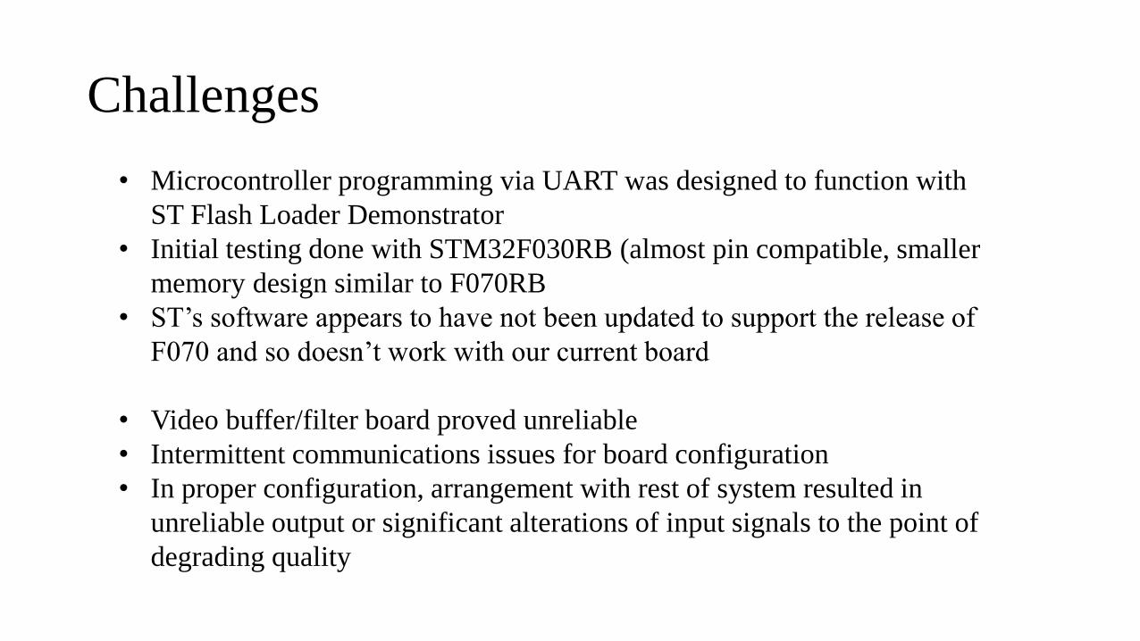
• Microcontroller programming via UART was designed to function with
ST Flash Loader Demonstrator
• Initial testing done with STM32F030RB (almost pin compatible, smaller
memory design similar to F070RB
• ST’s software appears to have not been updated to support the release of
F070 and so doesn’t work with our current board
• Video buffer/filter board proved unreliable
• Intermittent communications issues for board configuration
• In proper configuration, arrangement with rest of system resulted in
unreliable output or significant alterations of input signals to the point of
degrading quality

ADV7181D Development Board
• Known good hardware configuration
for testing ADV7181D
• Purchased after initial revisions of
video decoder board failed
• Ultimately allowed prototyping of
full system to continue
• ~$600

Results
MCU BoardFPGA Dev
Board
Video Decoder
Dev Board

Results
Super Doubler Output Composite Output
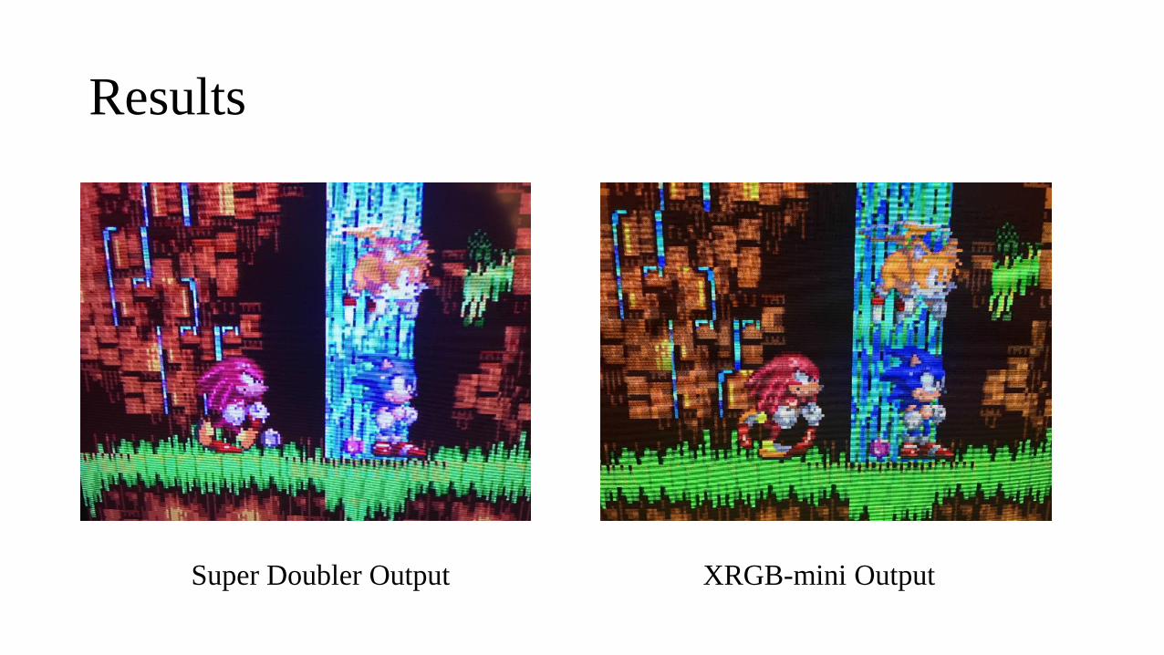
Results
Super Doubler Output XRGB-mini Output

Results
Super Doubler Scanlines Real Scanlines

Part Name Unit Cost Quantity TotalPower System Components Set ~$30 3 $90THS 7353 Video Buffer $3 3 $9AD1871 Audio Decoder $10 3 $30ADV7181 Video Decoder $14 3 $42STM32F070RBT6 MCU IC $2 3 $6Miscellaneous ICs - Varies $50Barrel Jacks (RCA, Power, etc) $1 10+ $10Miscellaneous Jacks - Varies $50
Miscellaneous Components - Varies $50PCB Fab/acquisition $50 1 $50Enclosure $10 1 $10Remote/Receiver Components $10 1 $10SD Card $10 1 $10Development Boards and Tools ~$150 Varies $150Total $567
Estimated Budget

Part Name TotalTHS 7353 Video Buffer $9ADV7181 Video Decoder $36STM32F070RBT6 MCU IC $6Miscellaneous ICs $10Barrel Jacks (RCA, Power, etc) $10Miscellaneous Jacks $15
Miscellaneous Components $50PCB $300+Soldering Materials $35Remote/Receiver Components $10SD Card $10Development Boards and Tools $1150Total Budget $1650+
Current Expenses

Division of Labor
• Stephen: FPGA development, video processing
• Kenneth: MCU interfacing, peripherals, MCU programming
• Gilson: video filtering, video decoder
• Tyler: manufacturing, testing, administrative

Questions?