THE SELF-HEATING EFFECTS OF BIPOLAR JUCTION …
131
THE SELF-HEATING EFFECTS OF BIPOLAR JUCTION TRANSISTORS ON THE FUNCTIONALITY OF A CURRENT FEEDBACK AMPLIFIER by XUESONG XIE Presented to the Faculty of the Graduate School of The University of Texas at Arlington in Partial Fulfillment of the Requirements for the Degree of DOCTOR OF PHILOSOPHY THE UNIVERSITY OF TEXAS AT ARLINGTON MAY 2010
Transcript of THE SELF-HEATING EFFECTS OF BIPOLAR JUCTION …

THE SELF-HEATING EFFECTS OF BIPOLAR JUCTION TRANSISTORS
ON THE FUNCTIONALITY OF A CURRENT FEEDBACK AMPLIFIER
by
XUESONG XIE
Presented to the Faculty of the Graduate School of
The University of Texas at Arlington in Partial Fulfillment
of the Requirements
for the Degree of
DOCTOR OF PHILOSOPHY
THE UNIVERSITY OF TEXAS AT ARLINGTON
MAY 2010

Copyright © by Xuesong Xie 2010
All Rights Reserved

iii
ACKNOWLEDGEMENTS
I would like to gratefully and sincerely thank Dr. Ronald L. Carter, Dr. Alan Davis, and
Dr. Howard T. Russell for their guidance, understanding, patience, and most importantly, their
friendship and moral support during my graduate studies. Their mentorship was paramount in
helping me finish the dissertation. Throughout my graduate studies, they encouraged me to
grow as independent thinker. For everything you have done for me, Dr. Ronald L. Carter, Dr.
Alan Davis, and Dr. Howard T. Russell, I thank you.
I would like to thank Dr. Jonathan Bredow and Dr. Jung-chih Chiao for serving in my
comprehensive examination and final dissertation defense committee. I would also like to thank
all of the members of the Analog IC Design group, who has helped with my studies, especially
Kamal Ranjan Sinha, Mingsheng Peng, AKM Sydul Haque, Ardasheir S Rahman, Zheng Li and
Zhipeng Zhu.
I would also acknowledge the Department of Electrical Engineering in the University of
Texas at Arlington for the financial support during my dissertation work.
Finally, I would like to thank my parents for their faith and encouragement in me. Also, I
thank my sisters who provided me with unending encouragement and support.
April 29, 2010

iv
ABSTRACT
THE SELF-HEATING EFFECTS OF BIPOLAR JUCTION TRANSISTORS
ON THE FUNCTIONALITY OF A CURRENT FEEDBACK AMPLIFIER
Xuesong Xie, PhD
The University of Texas at Arlington, 2010
Supervising Professor: Ronald L. Carter
Self-heating effects strongly affect the performance of modern silicon-on-insulator (SOI)
bipolar junction transistors. This research work does an extensive analysis of self-heating
effects on large-signal behavior, small-signal behavior and transient operation of bipolar junction
transistors. The two mechanisms in which device temperature affects large-signal behavior of a
BJT transistor are investigated, i.e. the common-emitter (CE) configuration is to be driven by a
constant base-emitter voltage and a constant base current. It is shown that the output
characteristic of a BJT transistor is less sensitive to self-heating under a fixed base current than
a fixed base-emitter voltage. A simple method of extracting the thermal resistance and the Early
voltage is proposed. Self-heating effects on the BJT small-signal behavior are examined by
investigating the two-port network parameters. It is shown that the gain of an amplifier and the
output impedance of a current mirror can be affected significantly by self-heating effects. The
mechanism of self-heating in transient operation is investigated and the transient operation of a
high speed voltage buffer is analyzed. A method for estimating the thermal tail of a voltage
buffer is presented.
An approach to analyze the contribution of each transistor to the overall thermal tail of
current feedback operational amplifiers is presented. It is shown that the overall thermal tail of a

v
current feedback operational amplifier (CFOA) is a linear superposition of each individual
transistor. Techniques to minimize the thermal tail are proposed. A cascode bootstrapped
CFOA is designed and optimized to minimize the thermal tail. The overall thermal tail is reduced
to 9 μV/V compared with 1032 μV/V of a classical CFOA when driving a 2 kΩ load in a unity
gain feedback configuration. Also the common mode rejection ratio (CMRR) is greatly improved
to 92 dB compared with 60 dB of the classical CFOA.
The Vertical Bipolar Inter Company (VBIC) model is used for all the simulations.
Simulations are performed using Cadence and Advanced Design System (ADS).

vi
TABLE OF CONTENTS
ACKNOWLEDGEMENTS ...............................................................................................................iii ABSTRACT.................................................................................................................................... iv LIST OF ILLUSTRATIONS ............................................................................................................ ix LIST OF TABLES..........................................................................................................................xiii Chapter Page
1. INTRODUCTION AND ORGANIAZTION……………………………………..………..….. 1
2. THE SPICE GUMMEL-POON AND VERTICAL BIPOLAR INTER-COMPANY
MODEL ..................................................................................................................... 3
2.1 SPICE Gummel-Poon (SGP) Model................................................................ 3
2.1.1 The Equivalent Circuit of the SGP Model and Related Parameters ................................................................................. 4
2.1.2 The SGP Model Formulation ........................................................... 4
2.2 Vertical Bipolar Inter-Company (VBIC) Model ................................................. 8
2.2.1 The Equivalent Circuit of the VBIC Model and Related
Parameters ................................................................................. 8 2.2.2 The VBIC Model Formulation ........................................................ 12
2.3 Conversion of the SGP to the VBIC Model ................................................... 17 2.4 Physics Based SGP and VBIC Model ........................................................... 18 2.5 Summary.......................................................................................................21
3. THE CURRENT FEEDBACK OPERATIONAL AMPLIFER.........................................22
3.1 Introduction to Current Feedback Operational Amplifier ............................... 22
3.1.1 Current Feedback Operational Amplifier Topology ....................... 22 3.1.2 Bandwidth Independent of Gain .................................................... 24 3.1.3 Stability Criterion ...........................................................................26

vii
3.2 Input Offset Voltage ...................................................................................... 27 3.3 Input Bias Current ......................................................................................... 30 3.4 Input Noise ....................................................................................................30 3.5 Common Mode Rejection Ratio ....................................................................31 3.6 Power Supply Rejection Ratio.......................................................................33 3.7 Common Mode Input Range .........................................................................34 3.8 Summary.......................................................................................................35
4. MODELING AND CHARACTERIZATION OF THE EFFECTS OF SELF-HEATING ON LARGE-SIGNAL BEHAVIOR OF A BJT TRANSISTOR...................................36
4.1 Thermal Effects of Self-Heating ....................................................................36
4.2 Large-Signal Behavior of BJT Transistor ...................................................... 37
4.2.1 Temperature Effects on the Model Parameters ............................ 37 4.2.2 Collector Current of a Current Driven Transistor ........................... 41 4.2.3 Large-Signal Behavior of a Current Driven Transistor................... 44 4.2.4 Large-Signal Behavior of a Constant Base-Emitter Voltage
Driven BJT Transistor................................................................ 49 4.3 A Method for Extraction of the Early Voltage and Thermal Resistance.........52
4.3.1 Theory ........................................................................................... 52 4.3.2 Parameters Mapping .....................................................................54 4.3.3 Procedure for Extraction................................................................ 55 4.3.4 Simulation Results.........................................................................56
4.4 Summary.......................................................................................................60
5. SELF-HEATING EFFECTS ON BJT SMALL-SIGNAL BEHAVIOR ............................. 61
5.1 Small-signal Model with Self-heating Effects ................................................ 61
5.2 Self-heating Effects on the Output Impedance of a Current Mirror ............... 67
5.3 Summary.......................................................................................................72
6. THE EFFECT OF SELF-HEATING IN TRANSIENT OPERATION.............................. 73

viii
6.1 Time Dependent Device Temperature .......................................................... 73 6.2 Self-Heating on Collector Current ................................................................ 75 6.3 Temperature Effects on the Base-Emitter Voltage........................................80
6.4 Self-Heating Effects on Transient Operation of Voltage Buffer ..................... 81
6.4.1 Voltage Buffer Biased with an Ideal Current Source .................... 81 6.4.2 Voltage Buffer Biased with a Current Mirror ..................................88
6.5 Summary.......................................................................................................92
7. DESIGN OF A SELF-HEATING TOLERANT CURRENT FEEDBACK
OPERATIONAL AMPLIFIER................................................................................... 93
7.1 Superposition of the Overall Thermal Tail in CFOA ......................................93 7.2 Cascode Bootstrapped CFOA ......................................................................97 7.3 Other CFOA Parameters............................................................................. 103
7.4 Summary.....................................................................................................108
8. CONLUSIONS AND FUTURE WORK .......................................................................109
APPENDIX
A. BIPOLAR JUNCTION TRANSISTOR MODLE FILE [10]........................................... 111 REFERENCES ........................................................................................................................... 114 BIOGRAPHICAL INFORMATION ............................................................................................... 118
ix
LIST OF ILLUSTRATIONS
Figure Page 2.1 Equivalent circuit of SGP static model [3] ................................................................................. 4 2.2 The variation of the total base resistance with base current ..................................................... 6 2.3 Equivalent circuit of VBIC model [3].......................................................................................... 9 2.4 The variation of the normalized depletion capacitance with junction voltage [5]. .................... 13 2.5 The effect of Rci on quasi-saturation [12] ................................................................................ 15 2.6 The effect of GAMM on quasi-saturation [12] .........................................................................15 2.7 The effect of VO on quasi-saturation [12] ................................................................................ 16 2.8 Current gain βF versus IC for an NPN transistor ......................................................................19 2.9 Transition frequency fT versus IC for an NPN transistor .......................................................... 20 2.10 Current gain βF versus IC for a PNP transistor ......................................................................20 2.11 Transition frequency fT versus IC for a PNP transistor........................................................... 21 3.1 Classical simplified CFOA circuit [21] ..................................................................................... 23 3.2 Simplified block diagrams of CFOA [25] ................................................................................. 24 3.3 (a) Non-inverting amplifier configuration [21], (b) Equivalent Macro-model of a CFOA in the non-inverting configuration [16] ...................... 25 3.4 CFOA input buffer [21]. ...........................................................................................................28 3.5 Alternative CFOA input buffer [21] .......................................................................................... 28 3.6 Eight transistors CFOA input buffer [24] ................................................................................. 29 3.7 Input bias current of CFOA .....................................................................................................30 3.8 Input noise of CFOA [24].........................................................................................................31 3.9 Small-signal equivalent input stage of the CFOA in figure 3.1 With a common-mode voltage applied [17]............................................................................. 32 3.10 CFOA in unity-gain configuration for simulation of PSRR+/- [20] ...........................................34

x
3.11 CMIR simulation configuration [21] ....................................................................................... 35 4.1 Electrothermal model for an SOIBJT ...................................................................................... 37 4.2 Ebers-Moll static model for an NPN ideal transistor: transport version [11] with thermal heating. ............................................................................................................... 38 4.3 Electron mobility and hole mobility temperature dependence When N=1017 cm-3................................................................................................................... 41 4.4 Bipolar transistor output characteristic showing the Early voltage, VA ....................................44 4.5 Forward Gummel plot.............................................................................................................. 56 4.6 Forward Gummel plot with TA=298 K ...................................................................................... 57 4.7 Transport saturation current versus temperature. ...................................................................58 4.8 Ideal base-emitter saturation current versus temperature....................................................... 58 4.9 DC Response with constant IB=2 μA, TA=298K ......................................................................59 4.10 DC Response with constant VBE=819.1 mV, TA=298K.......................................................... 59 5.1 Simplified BJT small-signal equivalent circuit with Self-heating effects included [38] ............................................................................................ 62 5.2 Admittance-parameter, two-port equivalent circuit [33] ........................................................... 63 5.3 Poles and zero of the output impedance with self-heating included .......................................65 5.4 A common-emitter amplifier with a current source load driven by a voltage source ............... 66 5.5 The gain magnitude of the amplifier shown in figure 5.4......................................................... 67 5.6 A simple current mirror and its output impedance simulation configuration ............................ 68 5.7 The magnitude of the output impedance of the simple current mirror in figure 5.6 ................. 68 5.8 Cascode current mirror and its output impedance simulation configuration............................ 70 5.9 The magnitude of the output impedance of the cascode current mirror in figure 5.8. ............. 70 5.10 Wilson current mirror and its output impedance simulation configuration ............................. 71 5.11 The magnitude of the output impedance of the Wilson current mirror in figure 5.10............. 71 6.1 Electro-thermal model of BJT..................................................................................................74 6.2 Typical curve of variation of the change in device temperature with time. .............................. 74 6.3 Typical curve of the variation of voltage with time...................................................................75

xi
6.4 A biased BJT with collector-emitter voltage changing............................................................. 77 6.5 First order temperature derivative of collector current with VBE=819.1 mV and VCE=4.15 V ............................................................................................... 78 6.6 Second order temperature derivative of collector current with VBE=819.1 mV and VCE=4.15 V. ............................................................................................... 78 6.7 First order collector-emitter voltage derivative of collector current With VBE=819.1 mV and TA=27 C ........................................................................................... 79 6.8 Second order collector-emitter voltage derivative of collector current with VBE=819.1 mV and TA=27 C.....................................................................................................79 6.9 Variation of collector current with VCE when With and without self-heating effects VBE=819.1 mV and TA=27 C....................................................................................................80 6.10 The variation of the base-emitter voltage with temperature For NPN and PNP transistors at 200 μA.................................................................................. 81 6.11 Voltage buffer biased with ideal constant current source...................................................... 82 6.12 The variations of collector current and base-emitter voltage Of Q2 with time after initial input step based on equation (6.19) ............................................. 86 6.13 The simulated variations of collector current and base-emitter Voltage of Q2 with time after initial input step..........................................................................87 6.14 The variations of collector current and base-emitter voltage Of Q4 with time after initial input step based on equation (6.19) ............................................. 87 6.15 The simulated variations of collector current and base-emitter Voltage of Q4 with time after initial input step..........................................................................88 6.16 Voltage buffer biased with current mirror .............................................................................. 89 7.1 Complete circuit of the classical CFOA in figure 3.1 With emitter degeneration resistors of 1kΩ ............................................................................. 94 7.2 Overall large-signal transient response of the CFOA in figure 7.1 With input driven by a 2 V peak to peak square wave, in unity-gain Non-inverting configuration with feedback resistor of 800 Ω .................................................... 94 7.3 A CFOA in the non-inverting amplifier configuration ............................................................... 96 7.4 Four possible cascode half-circuits of the input stage [40]...................................................... 98 7.5 Complete circuit of the CFOA with Wilson current mirror at the input and transimpedance stage. All transistors are 1x5 μm2 device. Emitter degeneration resistors are 1kΩ................................................................................... 99

xii
7.6 Overall large-signal transient response of the CFOA in figure 7.5 With input driven by a 2 V peak to peak square wave, in unity-gain Non-inverting configuration with feedback resistor of 800 Ω .................................................... 99 7.7 Complete circuit of the cascode reverse bootstrapped CFOA. Q23 and Q24 are cascode devices to improve the output resistance of Q9 and Q10, respectively....................................................................................................100 7.8 Overall large-signal transient response of the cascode reverse bootstrapped CFOA In figure 7.7 with input driven by a 2 V peak to peak square wave, in unity-gain Non-inverting configuration with feedback resistor of 800 Ω.................................................. 101 7.9 The overall thermal tails of the classic CFOA in figure 7.5 and the cascode bootstrapped CFOA in figure 7.7 when driving a load of 2 kΩ and 2 pF.................................................................................... 103 7.10 DC Current transfer curve of the cascode reverse bootstrapped CFOA in figure 7.7 ................................................................................................................ 104 7.11 Transimpedance of the cascode reverse bootstrapped CFOA in figure 7.7 ................................................................................................................ 105 7.12 Positive PSRR of the cascode reverse bootstrapped CFOA in figure 7.7 ................................................................................................................ 105 7.13 Negative PSRR of the cascode reverse bootstrapped CFOA in figure 7.7 ................................................................................................................ 106 7.14 DC voltage transfer curve of the cascode reverse bootstrapped CFOA in figure 7.7 ................................................................................................................ 106 7.15 CMRR of the cascode reverse bootstrapped CFOA in figure 7.7 ................................................................................................................ 107 7.16 CMIR of the cascode reverse bootstrapped CFOA in figure 7.7 ................................................................................................................ 107

xiii
LIST OF TABLES
Table Page 2.1 VBIC Model parameters and physical definition [12]............................................................... 10
2.2 Mappings from SGP parameters to VBIC parameters [3] ....................................................... 18
4.1 n and m corresponding to different doping level .....................................................................40 4.2 Extracted parameters.............................................................................................................. 57
4.3 Rth and VA at different VCE .......................................................................................................60
6.1 Theoretical VBE and IC of Q1 through Q8 at different time ........................................................ 91 6.2 Simulated VBE and IC of Q1 through Q8 at different time .......................................................... 92
7.1 Thermal tail obtained at terminal VO of the CFOA in figure 7.1 Caused by self-heating of each individual transistor, in unity-gain Non-inverting configuration with feedback resistor of 800 Ω [41] ............................................. 95 7.2 Thermal tail obtained at terminal VO of the CFOA in figure 7.5 And 7.7 caused by self-heating of each individual transistor, In unity-gain non-inverting configuration with feedback resistor of 800 Ω [41] ....................... 102

1
CHAPTER 1
INTRODUCTION AND ORGANIAZTION
Silicon-on-insulator (SOI) technology used in today’s applications has many advantages
over conventional bulk silicon, such as increased speed and simpler fabrication processes [1].
SOI-based devices differ from conventional silicon built devices in that silicon junction is above
an electrical insulator, which is typically silicon dioxide. The dielectrically isolated process allows
the creation of NPN and PNP transistors with highly complementary characteristics, yet isolated
from each other by insulator sidewalls [2]. It also gives low parasitic capacitance because of full
isolation and no P-N junction between the collectors and substrate or well. However, due to
poor heat conductivity of silicon dioxide, the use of a buried silicon dioxide layer causes larger
thermal spreading impedance which leads to more heat retention. This in turn increases the
operating temperature of the device and thus affects circuit behavior. The thermal effect
induced by the thermal spreading impedance is called the self-heating effect. The self-heating
effect is typically restricted to the heat generated by the device itself. Self-heating effects can be
significant for SOI-based bipolar junction transistors (BJTs) since the BJT performance is
strongly temperature dependent.
The self-heating effect on large-signal behavior, small-signal behavior and transient
operation of a bipolar junction transistor has been studied through analytical formulations and
simulations in this research work. A simple method of extracting thermal resistance and the
Early voltage has been developed based on the self-heating effects on large-signal behavior of
a BJT. Self-heating effects on the fundamental blocks of current feedback operational amplifiers
such as current mirror and voltage buffer has been studied. Based on this, a cascode
bootstrapped circuit topology is proposed to minimize the self-heating effect.

2
Chapter 2 introduces the SPICE Gummel-Poon (SGP) model and the Vertical Bipolar
Inter-Company (VBIC) model and conversions between these two models. Also the physics
based SGP and VBIC model used in this research work is introduced.
Chapter 3 provides an overview of current feedback operational amplifiers (CFOAs). It
presents the classical circuit topology of the CFOA, and the advantages and disadvantages of
CFOAs. Important operational amplifier parameters such as Input offset voltage, input bias
current, input noise, common mode rejection ratio, power supply rejection ratio, and common
mode input range are discussed in this chapter.
Chapter 4 provides an approach to model the self-heating effect on large-signal
behavior of BJT transistor. The two mechanisms in which device temperature affects large-
signal behavior of BJT transistor are discussed, i.e. common-emitter (CE) configuration is to be
driven by a constant base-emitter voltage and a constant base current. Also a simple method of
extracting the thermal resistance and the Early voltage is presented.
Chapter 5 presents the BJT small-signal model with self-heating effects. Self-heating
effects on BJT small-signal behavior are examined by investigating the two-port network
parameters. Self-heating effects on the output impedance of a current mirror are the primary
focus. Techniques to reduce self-heating effects are also discussed.
Chapter 6 provides an approach to model the self-heating effect in the transient
operation of a transistor. The effect of self-heating on transient operation in the high speed
voltage buffer is analyzed here.
Chapter 7 presents an approach to analyze the contribution of each transistor in an
operational amplifier to the overall thermal tail of current feedback amplifiers. Various design
techniques are suggested to develop self-heating tolerant CFOAs. A cascode bootstrapped
CFOA is proposed that minimize the self-heating effect.
Chapter 8 presents the summary of the accomplishments and the suggestions for future
work.

3
CHAPTER 2
The SPICE GUMMEL-POON AND VERTICAL BIPOLAR INTER-COMPNAY MODEL
The dielectrically isolated process allows the creation of NPN and PNP transistors with
highly complementary characteristics, and isolated from each other by insulator sidewalls. It
also gives low parasitic capacitance because of full isolation and no P-N junction between the
collectors and substrate or well. Dielectrically isolated bipolar junction transistors can be used to
design class AB output stages with very low quiescent current and high output drive in the
analog circuits used in wired broadband applications [2]. However, because of the use of a
buried oxide layer, it has large thermal resistance which causes heat retention which in turn
leads to circuit behavior. To accurately predict and simulate circuit behavior, an accurate model
is needed. While the widely used SPICE Gummel-Poon (SGP) model does not support the self-
heating effect, the improved Vertical Bipolar Inter-Company model (VBIC) does. This chapter
introduces the SGP model, VBIC model and conversions between these two models.
2.1 SPICE Gummel-Poon (SGP) model
The SPICE Gummel-Poon (SGP) model had been the industry standard bipolar
transistor model for more than 20 years before the VBIC model was developed by McAndrew’s
group in 1995 [3]-[5]. The SGP model shown in figure 2.1 was an improvement to the Ebers-
Moll model by modeling such second-order effects as the low-current effect (low-current drop in
β), the base-width modulation and the high-level injection [5]. To improve low current effect
modeling, two non-ideal diodes, DSE and DSC, are added to the Ebers-Moll model to represent
the base-emitter and base-collector recombination effect respectively. The normalized majority
base charge, qb, is introduced to model the base-width modulation effect and high-level injection
effect.

4
2.1.1 The Equivalent Circuit of the SGP Model and Related Parameters
Figure 2.1 shows the equivalent circuit of the SGP static model for the NPN bipolar
transistor [3]. It contains three nodes, i.e. Base (B), Emitter (E) and Collector (C). The depletion
capacitances, Cje and Cjc, model the incremental fixed charges Qje and Qjc stored in the base-
emitter and base-collector junction depletion regions for incremental changes in the associated
junction voltage respectively. The diffusion capacitances, Cbc and Cbe, model the diffusion
charges associated with the mobile carrier in the BJT. The three parasitic resistances, Rb, Re
and Rc, model the parasitic resistances at the base, emitter and collector respectively. Note Rb
is a current dependent resistance modulated by the normalized base charge, qb. The
capacitance, Cjcx, is used to model the distributed base-collector capacitance.
D SC
DSE
bcibcn
ben beicc
bcjc
bbi
jcx
e
c
beje
i
i
i
D F
D R
c
b
Figure 2.1 Equivalent circuit of SGP static model [3].
2.1.2 The SGP Model Formulation
2.1.2.1 The Collector and Base Currents of the SGP Model
The base current formulation considers the base-emitter and base-collector
recombination effect in the low-current region. Thus it has four components, i.e. the ideal
forward base-emitter diffusion current which flows through the diode, DF, and has a saturation
current, Ibei=IS/βF; the ideal reverse base-collector diffusion current which flows through the
5
diode, DR, and has a saturation current, Ibci= IS/βR; the non-ideal base-emitter recombination
current which flows through the diode, DSE, and has a saturation current, Iben=ISE; the non-ideal
base-collector recombination current which flows through the diode, DSC, and has a saturation
current, Ibcn=ISC. It can be formulated as [11]
1exp1exp
1exp1exp
TC
BCSC
TR
BC
R
S
TE
BESE
TF
BE
F
Sb
VNV
IVN
VI
VNVI
VNVI
I
(2.1)
where IS, ISE, ISC denote the transport saturation current, base-emitter leakage saturation current,
base-collector leakage saturation current respectively, NF, NE, NR and NC are ideality factors,
and F , R are the forward and reverse current gain.
The collector current has three components, i.e. the single current source, Icc, between
the collector and the emitter, which is a combination of the ideal forward diffusion current and
the ideal reverse diffusion current; the ideal reverse base-collector diffusion current which flows
through the diode, DR; the non-ideal base-collector recombination current which flows through
the diode, DSC. It is formulated as [11]
1exp1exp
1exp1exp
TC
BCSC
TR
BC
R
S
TR
BC
TF
BE
b
Sc
VNVI
VNVI
VNV
VNV
qII
. (2.2)
The charge, qb, denotes the normalized base charge in equation (2.2) and is [11]
)411(2 2
1 qqqb , (2.3)
AR
BC
AF
BE
VV
VVq
1
11 , (2.4)

6
1exp1exp2
TR
BC
KR
S
TF
BE
KF
S
VNV
II
VNV
IIq . (2.5)
The variables, VAF, VAR, IKF and IKR, are the forward Early voltage, the reverse Early voltage, the
forward high-level injection knee current and the similar reverse current respectively. Note that
q1 models the effects of base-width modulation and q2 models the effect of high-level injection.
2.1.2.2 Current Dependence of the Base Resistance
The base resistance consists of the external base resistance (Rb) and the intrinsic base
resistance (Rbm). The external base resistance includes the contact resistance and sheet
resistance. The intrinsic base resistance is a function of base current. The current dependence
of this resistance comes from nonzero base region resistivity, which in turn precipitates non-
uniform biasing of the base-emitter junction.
The total base resistance is [11]
zzzzRRRR bmbbmbbi 2tan
tan3
, (2.6)
rBb
rBb
IIII
z 2
2
2414411
. (2.7)
Figure 2.2 The variation of the total base resistance with base current

7
Figure 2.2 shows the typical curve of the variation of the total base resistance with the base
current. The variable Rbm is the minimum base resistance that occurs at high currents, Rb is the
base resistance at zero bias (small base currents), IrB is the current where the base resistance
falls halfway to its minimum value.
2.1.2.3 Temperature Mappings of the SGP Model
BJT electrical behavior varies with temperature, so the SGP model defines the
temperature dependence for its model parameters. The saturation current depends on the
intrinsic carrier concentration and the diffusion coefficient of electrons and holes. Temperature
appears explicitly in the exponential terms of the equations of both the intrinsic carrier
concentration and the diffusion coefficient. The temperature dependence of the transport
saturation current is determined by [11]
1
2
21
212 1
)300(exp)()(
TT
kTqE
TTTITI g
XTI
SS . (2.8)
The variables, XTI and Eg, are the saturation current temperature exponent and the energy gap.
The effect of temperature on forward and reverse current gain is determined by [11]
XTB
RR
XTB
FF
TTTT
TTTT
1
212
1
212
)(
)(
. (2.9)
The temperature dependence of the junction built-in potential, J , is modeled as
follows: [11]
21
1
2
1
221
1
22 ln3 TETE
TT
TT
qkTT
TTT ggJJ . (2.10)

8
2.2 Vertical Bipolar Inter-Company (VBIC) Model
The SPICE Gummel-Poon (SGP) model had been the industry standard for circuit
simulation for over 20 years. However, the SGP model has some shortcomings, e.g. it is unable
to model collector resistance modulation (quasi-saturation) and parasitic substrate transistor
action. Improved BJT models have been presented over the years [6]-[7]. In 1995 a group of
representatives from the IC and CAD industries defined the VBIC model to replace the SGP
model. The complete source code for the VBIC model is accessible to the public. It was made to
be as similar to the SGP model as possible.
2.2.1 The Equivalent Circuit of the VBIC Model and Related Parameters
Figure 2.3 shows the equivalent circuit for the VBIC model [3]. It contains five nodes, i.e.
Base (B), Emitter (E), Collector (C), Substrate (S) and a temperature rise node that models self-
heating (dT). The VBIC model includes a NPN transistor modeled by a complete Gummel-Poon
model and a parasitic substrate PNP transistor modeled by a simplified Gummel-Poon model. A
weak avalanche current Igc is included for the base-collector junction. Quasi-saturation is
modeled with the elements Rci, Cbcx, and Cbcq [4]. The constant capacitance, CBEO and CBCO, are
included to model capacitances associated with extrinsic base-emitter and base-collector
overlap capacitance respectively. The intrinsic base resistance and parasitic base resistance,
Rbi, and Rbip, are modulated by the normalized base charges, qb and qbp. The intrinsic collector
resistance, Rci, is modulated by Vbci. Two additional sub-circuits are included to model excess
phase effect and self-heating effect. The excess phase effect is modeled by a second-order
RLC network. Self-heating is modeled by the thermal power source Ith and a RC thermal
network which includes the thermal resistance Rth and capacitance Cth. The thermal power
source Ith couples the power generated in the transistor to the thermal network. The local
temperature rise at node dT is linked to the electrical model through the temperature mappings
of the model parameters.
9
bci gcbcn
ben bei
bcjcbcq
ben bei
b b
bcx
bip bp
bcpn
bepnjep
jcpbcpi
bepi bep
cp
jex
s
bx
e
cx
ci
BCO
BEO
beje
x
i
x
i
i
i
p
cc
th ththcc
F1 F2
cxf
lxf
Figure 2.3 Equivalent circuit of VBIC Model [3].
Overall the VBIC model improves the deficiencies of the Gummel-Poon model in the
following aspects [5]: the Early effect modeling, parasitic substrate PNP modeling, quasi-
saturation modeling, weak avalanche modeling, constant parasitic overlap capacitance
modeling, excess phase modeling, temperature dependency modeling and self-heating
modeling.
Table 2.1 lists each parameter of the VBIC model and gives a short description of the
function of the parameter.

10
Table 2.1 VBIC Model parameters and physical definition [12]
VBIC Parameters Definition
Main Collector Current Source IS Transport saturation current NF Forward emission coefficient NR Reverse emission coefficient
Early Effect Modeling VEF Forward Early Voltage (0=infinity) VER Reverse Early Voltage (0=infinity)
Webster Effect IKF Forward knee current IKR Reverse knee current
Forward Base Current IBEI Ideal base-emitter saturation current NEI Ideal base-emitter emission coefficient IBEN Non-ideal base-emitter saturation current NEN Non-ideal base-emitter emission coefficient WBE Portion of IBEI from VBEI, 1-WBE from VBEX
Reverse Base Current IBCI Ideal base-collector saturation current NCI Ideal base-collector emission coefficient IBCN Non-ideal base-collector saturation current NCN Non-ideal base-collector emission coefficient
Weak Avalanche Current AVC1 Base-collector weak avalanche parameter 1 AVC2 Base-collector weak avalanche parameter 2
Parasitic Resistance RE Emitter resistance RBX Extrinsic base resistance RBI Intrinsic base resistance RS Substrate resistance RBP Parasitic base resistance RCX Extrinsic collector resistance
Quasi Saturation RCI Intrinsic collector resistance GAMM Epi doping parameter VO Epi drift saturation voltage HRCF High current RC factor QCO Collector charge at zero bias
Space Charge Capacitance CJE Base-emitter zero-bias junction capacitance PE Base-emitter grading coefficient ME Base-emitter junction exponent AJE Base-emitter capacitance smoothing factor CJC Base-collector zero-bias junction capacitance PC Base-collector grading coefficient MC Base-collector junction exponent AJC Base-collector capacitance smoothing factor
11
CJEP Base-emitter extrinsic zero-bias junction capacitance CJCP Base-collector extrinsic zero-bias junction capacitance PS Collector-substrate grading coefficient MS Collector-substrate junction exponent AJS Collector-substrate capacitance smoothing factor FC Forward bias junction capacitance threshold
Transit Time Modeling TF Forward transit time XTF Coefficient of TF bias dependence ITF Coefficient of TF dependence on ICC VTF Coefficient of TF dependence on VBC QTF Variation of TF with base-width modulation TR Ideal reverse transit time
Excess Phase TD Forward excess-phase delay time
Parasitic Capacitance CBEO Extrinsic base-emitter overlap capacitance CBCO Extrinsic base-collector overlap capacitance
Parasitic Substrate Transistor ISP Parasitic transport saturation current NFP Parasitic forward emission coefficient WSP Portion of ICCP from VBEP, 1-WSP from VBCI IBEIP Ideal parasitic base-emitter saturation current IBENP Non-ideal parasitic base-emitter saturation current IBCIP Ideal parasitic base-collector saturation current NCIP Ideal parasitic base-collector emission coefficient IKP Parasitic current (0=infinity)
Temperature Mapping CTH Thermal capacitance RTH Thermal resistance TNOM Nominal ambient temperature for characterizing EA Activation energy for IS EAIE Activation energy for IBEI EAIC Activation energy for IBCI/IBEIP EAIS Activation energy for IBCIP EANE Activation energy for IBEN EANC Activation energy for IBCN/IBENP EANS Activation energy for IBCNP XRE Temperature exponent of emitter resistance XRC Temperature exponent of collector resistance XRB Temperature exponent of base resistance XRS Temperature exponent of substrate resistance XVO Temperature exponent of VO XIS Temperature exponent of IS XII Temperature exponent of IBEI/IBCI/IBEIP/IBCIP XIN Temperature exponent of IBEN/IBCN/IBENP/IBCNP TNF Temperature exponent of NF TAVC Temperature exponent of AVC
Noise Modeling KFN Flicker noise coefficient
Table 2.1 – Continued
12
AFN Flicker noise exponent BFN Flicker noise frequency exponent
2.2.2 The VBIC Model Formulation
2.2.2.1 Collector current and base current of VBIC model
The core of the VBIC model is the transport current model, which is similar to the SGP
model. The collector transport current is related to the forward transport current (Itf) and the
reverse transport current (Itr) and determined by [5]
1exp
1exp
/)(
kTNqVIIkTNqVII
qIII
RbciStr
FbeiStf
btrtfcc
. (2.11)
The variables, Vbei and Vbci, are the voltage difference between node Bi and Ei and the voltage
difference between node Bi and Ci in figure 2.3. Non-ideal factors NF and NR are included for
forward and reverse components of Icc, for compatibility with the SGP model.
The collector transport current of the VBIC model has the same form as the SGP model,
but the normalized base charge, qb, is modeled differently. For the VBIC model, the normalized
base charge includes depletion and diffusion components. The normalized base charge is [5]
bb q
qqq 21 , (2.12-a)
where
1exp1exp
1
2
1
kTNqV
II
kTNqV
IIq
Vq
Vq
q
R
bci
KR
S
F
bei
KF
S
EF
jc
ER
je
. (2.12-b)
The variables, VEF and VER, are the forward and reverse Early voltage, while IKF and IKR are the
forward and reverse knee currents. The Early voltage components model the base-width
modulation effect and the knee current components model the high-level injection effect. The
normalized base-emitter and base-collector depletion charges are [5]
Table 2.1 – Continued

13
.,,,,
,,,,,
JCCCCbcijjc
JECEEbeijje
AFMPVqqAFMPVqq
(2.13)
Here PE, PC and ME, MC are the built-in potentials and grading coefficients of the base-emitter
and base–collector junctions respectively, while AJE and AJC are the capacitance smoothing
factors of the base-emitter and base–collector junctions respectively. FC is the forward bias
junction capacitance threshold. The normalized depletion capacitance function for reverse and
low forward bias is [5]
MCj
Cj PVVAFMPVq
AFMPVC)1(
1),,,,(),,,,(
. (2.14)
If the depletion capacitance smoothing parameters AJE and AJC are less than zero, Cj limits its
value to a constant for V>FCP, otherwise Cj increases linearly just like the SGP model does in
figure 2.4.
-0.5 0 0.5 10
0.5
1
1.5
2
2.5
3
3.5
Vj (V)
C j
VBICSGP
Figure 2.4 The variation of the normalized depletion capacitance with junction voltage [5].
Instead of linking base current and collector current by beta, the base current is
modeled independently of the collector current in the VBIC model. The base current in the VBIC

14
model is also apportioned between the intrinsic and extrinsic components. The base-emitter
component of the intrinsic transistor base current is modeled as [5]
1exp1exp kTNqVIkTNqVIWI ENbeibenEIbeibeiBEbe . (2.15)
Here Ibei and Iben are ideal and non-ideal saturation currents, NEI and NEN are ideality factors.
Usually NEI is approximately equal to 1 and NEN is approximately 2. The base-collector
component is similarly modeled as [5]
1exp1exp kTNqVIkTNqVII CNbcibcnCIbcibcibc . (2.16)
The extrinsic base-emitter recombination current is determined by [5]
1exp1exp1 kTNqVIkTNqVIWI ENbexbenEIbexbeiBEbex . (2.17)
The weak avalanche current, Igc, is modeled as [7]
121 exp)( ME
bciCVCbciCVCbcccgc VPAVPAIII . (2.18)
2.2.2.2 Quasi-Saturation
One of the major shortcomings of the SGP model is that it does not support quasi-
saturation modeling. The VBIC model modifies the Kull-Nagel model [5] to avoid the negative
output conductance problem at high VBE. The VBIC model also includes an empirical model for
modeling the increase of collector current at high Vbci. The intrinsic collector resistance, Rci, is
used to model quasi-saturation. The VBIC model gives the current in the modulated Rci as [5]
22
0
0
01.05.01.1
HRCFVV
VRI
II
O
rci
O
ciepi
epirci , (2.19-a)
where
tv
bcxbcx
tv
bcibci
bcx
bcibcxbcitvrci
ciepi
VVGAMMK
VvGAMMK
KKKKVV
RI
exp1,exp1
11ln.1
0
. (2.19-b)

15
Here Vrci = Vbci - Vbcx is the voltage across Rci, HRCF is the high current RC factor which
accounts for the increase of collector current at high Vbci, GAMM is the collector doping factor
parameter, and VO is the epitaxial drift saturation voltage. Figure 2.5 shows how Rci affects the
output characteristics. It basically determines the slope of the saturated range. With the
parameter GAMM, the effect of quasi-saturation is deferred to the higher currents as shown in
figure 2.6. The epitaxial drift saturation voltage, VO, determines the begin of velocity saturation.
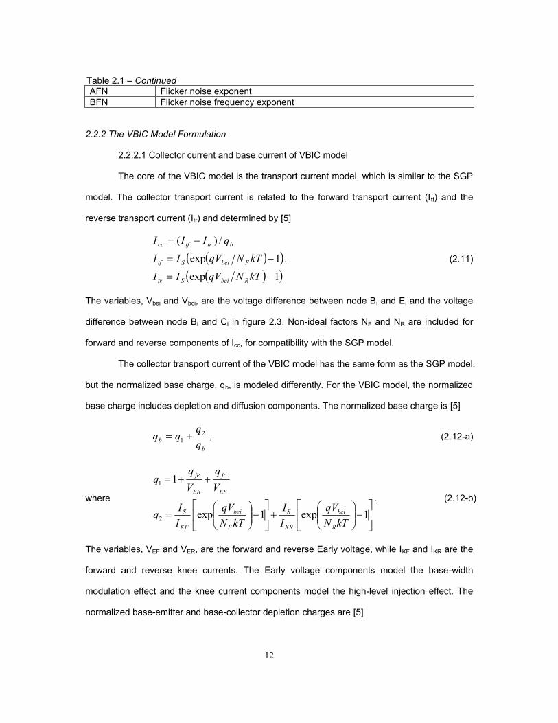
This means a smoothing at the high-end of the quasi-saturation as shown in figure 2.7 [12].
Figure 2.5 The effect of Rci on quasi-saturation [12]
Figure 2.6 The effect of GAMM on quasi-saturation [12]
16
Figure 2.7 The effect of VO on quasi-saturation [12]
2.2.2.3 Temperature Mappings of the VBIC Model
The temperature mappings of the VBIC model are similar to those of the SGP model.
The temperature dependence of the transport saturation current is [5]
FN
nom
XIS
nomnomSS T
TkTEAq
TTTITI
1
1exp)()(
. (2.20)
Here XIS is the temperature exponent and EA is the activation energy.
Each saturation current has a separate temperature exponent and also an activation
energy. The intrinsic base-emitter saturation current, Ibei, varies with temperature as [5]
EIN
nom
XII
nomnombeibei T
TkTEAIEq
TTTITI
1
2
1exp)()(
. (2.21)
NF, NR and AVC1 are modeled as having linear temperature dependence [5], i.e.
)()()( nomnomFF TTTNFTNTN , (2.22)
)()()( nomnomRR TTTNFTNTN , (2.23)
)()()( 11 nomnomVCVC TTTNVCTATA . (2.24)

17
The built-in potential P and zero bias junction capacitance Cj are modeled in a similar
way as the SGP model, with a modification to avoid the built-in potential going negative for high
temperature [9]. The built-in potential P varies with temperature as [13]
2)exp(411
ln2 kTqqkTTP
, (2.25)
where
1ln3
2exp
2expln2
nomnom
nom
nom
nom
nom
TTEA
TT
qkT
kTTqP
kTTqP
qkT
. (2.26)
The temperature dependence of the zero bias junction capacitance Cj is determined by [9]
Mnom
nomjj TPTPTCTC
)()( . (2.27)
The collector doping parameter, GAMM, is modeled over temperature as [6]
FN
nom
XIS
nomnom T
TkTEAq
TTTGAMMTGAMM
1
1exp)()(
. (2.28)
The collector drift saturation voltage, VO, is modeled over temperature as [5]
XVO
nomnomOO T
TTVTV
)()( . (2.29)
2.3 Conversion of the SGP to the VBIC Model
The treatment of the Early effect is the major difference between the VBIC and SGP
models. Thus most of the SGP model parameters can be converted to VBIC model parameters
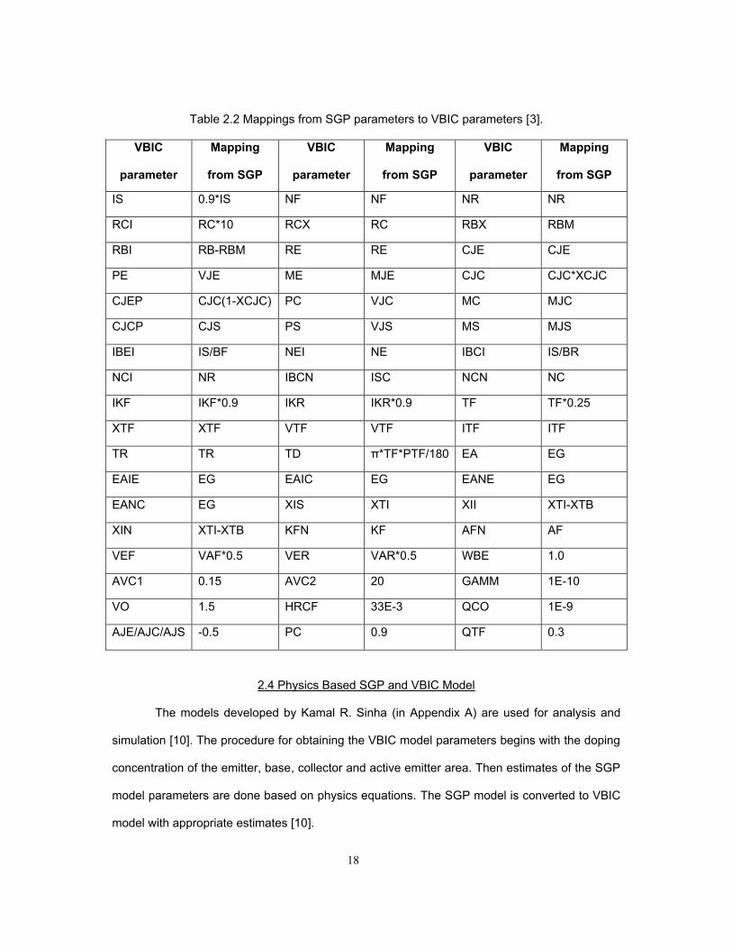
[3]. Table 2.2 lists simple mappings from SGP parameters to VBIC parameters as well as the
empirical or optimized values used for the additional features in the VBIC model.
18
Table 2.2 Mappings from SGP parameters to VBIC parameters [3].
VBIC
parameter
Mapping
from SGP
VBIC
parameter
Mapping
from SGP
VBIC
parameter
Mapping
from SGP
IS 0.9*IS NF NF NR NR
RCI RC*10 RCX RC RBX RBM
RBI RB-RBM RE RE CJE CJE
PE VJE ME MJE CJC CJC*XCJC
CJEP CJC(1-XCJC) PC VJC MC MJC
CJCP CJS PS VJS MS MJS
IBEI IS/BF NEI NE IBCI IS/BR
NCI NR IBCN ISC NCN NC
IKF IKF*0.9 IKR IKR*0.9 TF TF*0.25
XTF XTF VTF VTF ITF ITF
TR TR TD π*TF*PTF/180 EA EG
EAIE EG EAIC EG EANE EG
EANC EG XIS XTI XII XTI-XTB
XIN XTI-XTB KFN KF AFN AF
VEF VAF*0.5 VER VAR*0.5 WBE 1.0
AVC1 0.15 AVC2 20 GAMM 1E-10
VO 1.5 HRCF 33E-3 QCO 1E-9
AJE/AJC/AJS -0.5 PC 0.9 QTF 0.3
2.4 Physics Based SGP and VBIC Model
The models developed by Kamal R. Sinha (in Appendix A) are used for analysis and
simulation [10]. The procedure for obtaining the VBIC model parameters begins with the doping
concentration of the emitter, base, collector and active emitter area. Then estimates of the SGP
model parameters are done based on physics equations. The SGP model is converted to VBIC
model with appropriate estimates [10].
19
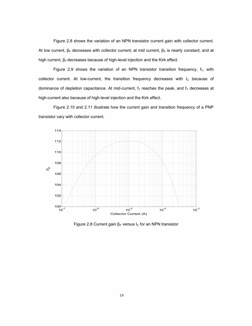
Figure 2.8 shows the variation of an NPN transistor current gain with collector current.
At low current, βF decreases with collector current; at mid current, βF is nearly constant; and at
high current, βF decreases because of high-level injection and the Kirk effect.
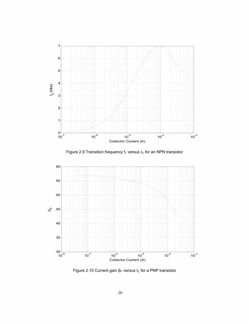
Figure 2.9 shows the variation of an NPN transistor transition frequency, fT, with
collector current. At low-current, the transition frequency decreases with IC because of
dominance of depletion capacitance. At mid-current, fT reaches the peak, and fT decreases at
high-current also because of high-level injection and the Kirk effect.
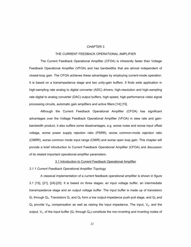
Figure 2.10 and 2.11 illustrate how the current gain and transition frequency of a PNP
transistor vary with collector current.
10-7 10-6 10-5 10-4 10-3100
102
104
106
108
110
112
114
Collector Current (A)
F
Figure 2.8 Current gain βF versus IC for an NPN transistor
20
10-7
10-6
10-5
10-4
10-3
0
1
2
3
4
5
6
7
Collector Current (A)
f T (Ghz
)
Figure 2.9 Transition frequency fT versus IC for an NPN transistor
10-8
10-7
10-6
10-5
10-4
10-3
30
35
40
45
50
55
60
Collector Current (A)
F
Figure 2.10 Current gain βF versus IC for a PNP transistor

21
10-8 10-7 10-6 10-5 10-4 10-30
0.5
1
1.5
2
2.5
3
3.5
4
4.5
Collector Current (A)
f T (Ghz
)
Figure 2.11 Transition frequency fT versus IC for a PNP transistor
2.5 Summary
The SGP model provides an improvement to the Ebers-Moll model in the areas of the
low-current effect, the base-width modulation effect and the high-level injection effect. The VBIC
formulation improves the SGP model in the modeling of the Early-effect, the self-heating effect,
inclusion of the parasitic substrate PNP transistor, quasi-saturation, weak avalanche, excess
phase and parasitic capacitance. The conversion between the SGP model and the VBIC model
is presented because the VBIC model is as similar to the SGP model as possible apart from the
improvements.
22
CHAPTER 3
THE CURRENT FEEDBACK OPERATIONAL AMPLIFIER
The Current Feedback Operational Amplifier (CFOA) is inherently faster than Voltage
Feedback Operational Amplifier (VFOA) and has bandwidths that are almost independent of
closed-loop gain. The CFOA achieves these advantages by employing current-mode operation.
It is based on a transimpedance stage and two unity-gain buffers. It finds wide application in
high-sampling rate analog to digital converter (ADC) drivers, high-resolution and high-sampling
rate digital to analog converter (DAC) output buffers, high-speed, high-performance video signal
processing circuits, automatic gain amplifiers and active filters [14] [15].
Although the Current Feedback Operational Amplifier (CFOA) has significant
advantages over the Voltage Feedback Operational Amplifier (VFOA) in slew rate and gain-
bandwidth product, it also suffers some disadvantages, e.g. worse noise and worse input offset
voltage, worse power supply rejection ratio (PSRR), worse common-mode rejection ratio
(CMRR), worse common mode input range (CMIR) and worse open loop gain. This chapter will
provide a brief introduction to Current Feedback Operational Amplifier (CFOA) and discussion
of its related important operational amplifier parameters.
3.1 Introduction to Current Feedback Operational Amplifier
3.1.1 Current Feedback Operational Amplifier Topology
A classical implementation of a current feedback operational amplifier is shown in figure
3.1 [15], [21], [24]-[25]. It is based on three stages: an input voltage buffer, an intermediate
transimpedance stage and an output voltage buffer. The input buffer is made up of transistors
Q1 through Q4. Transistors Q1 and Q2 form a low output-impedance push-pull stage, and Q3 and
Q4 provide VBE compensation as well as raising the input impedance. The input, Vp, and the
output, Vn, of the input buffer (Q1 through Q4) constitute the non-inverting and inverting nodes of

23
the CFOA. Summing currents at the inverting node yields In = I1 - I2, where I1 and I2 are the
push-pull transistors currents. A pair of current mirrors (Q13 ~ Q16) forms the intermediate
transimpedance stage. The transimpedance stage reflects the push-pull transistors currents (I1,
I2) and recombines them at a common high-impedance node Z. The voltage formed at the high-
impedance node, Z, is then transferred to the output via a second buffer. The output voltage
buffer is made up of transistors Q5 ~ Q8 and provides low-output impedance for the external
load. Transistors Q9 through Q12 and Q17 through Q18 provide biasing circuitry for the input
buffer and the output buffer respectively. Bias in the output stage is usually larger than that of
the input to provide an adequate output drive to the load. Figure 3.2 summarizes the current-
mode operation feature of a current feedback amplifier in a general block-diagram form.
Figure 3.1 Classical simplified CFOA circuit [21].

24
1
2
1
2
p on
Figure 3.2 Simplified block diagrams of CFOA [25].
3.1.2 Bandwidth Independent of Gain
The current feedback operational amplifier is widely used in high-frequency analog
signal processing, especially in the use of non-inverting amplifier configuration shown in figure
3.3 (a). One of the main advantages is that, unlike the constant Gain-Bandwidth product of the
VFOA, the amplifier’s closed-loop bandwidth is almost independent of its close-loop gain [21].
Figure 3.3 (b) shows the equivalent marco-model of a CFOA in the non-inverting
amplifier configuration. The resistance, Roinv, is the input buffer output resistance looking into
the inverting node Vn of the CFOA. The summing current flowing out of the input buffer In, is
replicated at the high-impedance node Z through a current controlled current source. Note that
In is also the difference between the feedback current If and the current flowing through Rg (Ig).
High Z node impedance is represented by Rt and Ct. The frequency, ωcm, is the current mirror
pole frequency due to the current mirror circuits showed in figure 3.2. Typically, the current
mirror pole frequency is much higher than the pole frequency of a high Z node due to high
impedance of node Z.

25
Figure 3.3 (a) Non-inverting amplifier configuration [21], (b) Equivalent Macro-model of a CFOA in the non-inverting configuration [16].
By assuming ωcm →∞, the transimpedance Zt (s) can be represented by the equivalent
Rt, Ct circuit as
t
tt s
RsZ
1
)( , (3.1)
where )(1 ttt CR . The loop gain T (s) can be represented as follows
f
t
RsZsT )(
)( . (3.2)
The voltage developed by high Z node in response of In is conveyed to the output through a
voltage buffer, which gives

26
)()( sZIsV tno (3.3)
Noting that the input buffer keeps Vin=Vp=Vn, the Kirchhoff’s Current Law (KCL) at the inverting
node gives
sVRR
sVI ogf
inn
11 (3.4)
Thus the simplified transfer function of figure 3.3 (a) can be obtained by combining equations
(3.3) and (3.4) as [21]
ft
tftft
t
g
f
g
f
in
o
RRCRsRRR
RRR
sTRR
sVsV
1
11
1111
)()(
. (3.5)
By assuming transresistance Rt>>Rf, the transfer function can be simplified as
tfg
f
in
o
CsRRR
sVsV
111
)()(
. (3.6)
Equation (3.4) shows that the closed loop bandwidth is determined by )(1 tf CR , and the
closed loop gain is determined by gf RR1 . Thus the gain and bandwidth can be
independently adjusted by choosing the value of Rf and Rg.
3.1.3 Stability Criterion
If the current mirror pole frequency, ωcm, is much greater than ωt, but not ∞, then the
transimpedance function Zt (s) becomes
cmt
tt ss
RsZ
11
)( . (3.7)
The transfer function of CFOA becomes [16]

27
22
2
2
1
1
1111
)()(
pp
p
g
f
cmtf
tcm
cmtf
t
g
f
g
f
in
o
sQ
sRR
RRss
RR
RR
sTRR
sVsV
, (3.8)
where tf
cmp CR
and
cmtfCRQ
1
.
Equation (3.6) is a classical two-pole characteristic equation. To avoid peaking, the
value of Q should be chosen to be less than 21 , and so Rf should be equal to or greater
than cmtC 2 . Hence a minimum feedback back resistance is required to ensure the stability
of the non-inverting configuration of the CFOA [16], [18], [21].
3.2 Input Offset Voltage
The input offset voltage in a CFOA suffers from component mismatches much more
than does a VFOA. Figure 3.4 shows the simplest implementation of the input stage of a CFOA.
The main problem of this configuration is that the input offset voltage will be affected by
mismatch between the NPN’s and PNP’s base-emitter voltage (VBE). Assuming no mismatch of
VBE and Early voltage for the same kind of transistors, the input offset voltage is given by [22]
41
32
1
2 ln2
lnln2 AA
AAVJJV
IIVV T
SN
SPT
Tos . (3.9)
where VT is the thermal voltage, I1 and I2 are the bias currents of the input stage, JSN and JSP
are the saturation current density of the NPN and PNP transistor respectively, An is the emitter

28
area of Qn. The second term will be the dominant contributor to the input offset voltage because
of the configuration.
1
4
3
2
1
2
CC
EE
P N
Figure 3.4 CFOA input buffer [21].
Another type of CFOA input stage is shown in figure 3.5 [21]. With the use of two diode
connected transistors, this configuration allows matching between the same kinds of transistors.
Therefore, it achieves better input offset voltage than the input stage in figure 3.4. However, the
tradeoff is relatively low non-inverting input impedance, a high non-inverting input bias current,
and noise.
Figure 3.5 Alternative CFOA input buffer [21].

29
The eight transistors input stage configuration [23]-[24] shown in figure 3.6 has the
advantage of high non-inverting input impedance, low non-inverting input bias current and low
input offset voltage due to base-emitter voltage matching of the same kinds of transistors. On
the other side, this configuration results in poor common mode input range due to the cascade
of transistors, slew rate limitation, relatively higher inverting output impedance and hence
relatively lower bandwidth for the CFOA.
Figure 3.6 Eight transistors CFOA input buffer [24].
The analysis of the half circuit gives
5361 BEQEBQBEQEBQNPos VVVVVVV . (3.10)
Assuming perfect matching between the same kinds of transistors and considering
Early voltage effect, equation (3.8) becomes [23]-[24]
1
3
6 Q
5 lnBCQAP
BCQAP
CBAN
CBQANTos VV
VVVVVV
VV . (3.11)
30
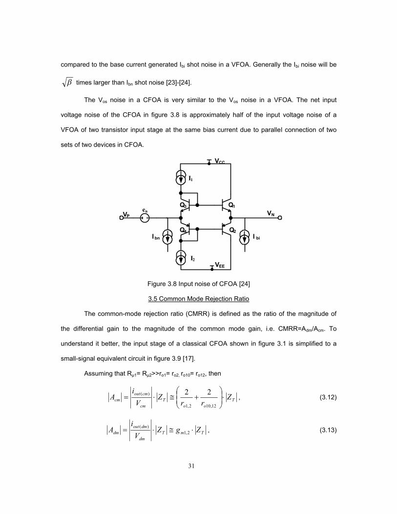
3.3 Input Bias Current
The current feedback operational amplifier generally has higher input bias current than
the voltage feedback operational amplifier. In the VFOA, the input bias currents are fairly well
matched, while in the CFOA the input bias currents are not well matched as discussed in
section 3.2. The non-inverting input error term (Ibn) which flows directly out of non-inverting
terminal is usually a result of mismatch between the upper branch and the lower branch of the
input buffer and mismatch of bias current (I1 and I2) [23]-[24]. The inverting input error item (Ibi)
which flows directly out of the inverting terminal is usually a result of input offset voltage,
feedback resistance Rf and Rg. The two mechanisms are not correlated.
EE
CC
3
4
1
2
NP
2
1
bn bi
Figure 3.7 Input bias current of CFOA
3.4 Input Noise
Noise in a CFOA is higher than that of a VFOA. The Ibn shot noise in both a CFOA and
VFOA is made up of base current, but in a CFOA there are usually two base currents due to the
use of a complementary input stage compared to one base current in a VFOA. The Ibn shot
noise in a CFOA is 2 times larger than that of a VFOA. For the Ibi noise, the CFOA and
VFOA are totally different. The Ibi shot noise in the CFOA is dominated by the collector currents
of the output transistors on the inverting side of the input buffer, which is a much larger current
31
compared to the base current generated Ibi shot noise in a VFOA. Generally the Ibi noise will be
times larger than Ibn shot noise [23]-[24].
The Vos noise in a CFOA is very similar to the Vos noise in a VFOA. The net input
voltage noise of the CFOA in figure 3.8 is approximately half of the input voltage noise of a
VFOA of two transistor input stage at the same bias current due to parallel connection of two
sets of two devices in CFOA.
EE
CC
3
4
1
2
NP
2
1
n
bn bi
Figure 3.8 Input noise of CFOA [24]
3.5 Common Mode Rejection Ratio
The common-mode rejection ratio (CMRR) is defined as the ratio of the magnitude of
the differential gain to the magnitude of the common mode gain, i.e. CMRR=Adm/Acm. To
understand it better, the input stage of a classical CFOA shown in figure 3.1 is simplified to a
small-signal equivalent circuit in figure 3.9 [17].
Assuming that Rμ1= Rμ2>>ro1= ro2, ro10= ro12, then
Too
Tcm
cmoutcm Z
rrZ
Vi
A
12,102,1
)( 22, (3.12)
TmTdm
dmoutdm ZgZ
Vi
A 2,1)( , (3.13)

32
12,102,1
2,1
22CMRR
oo
m
cm
dm
rr
gAA
, (3.14)
where Zt is the high impedance at the high Z node, iout(cm) and iout(dm) are the output currents of
the common mode and the differential mode, respectively, Vcm and Vdm are the input common-
mode voltage and differential-mode voltage, respectively.
μ1m3
m1 be1b1 o1in(cm)
μ2m4
m2 be2b2 o2in(cm)
cm
cm
o10
o12
out(cm)
out(cm)
1
2
1
2
Figure 3.9 Small-signal equivalent input stage of the CFOA in figure 3.1 with a common-mode voltage applied [17].
The CMRR for the CFOA depends on the output resistances of the bias current mirrors
(Q9 through Q10 and Q11 through Q12 in figure 3.1) in the input stage and the output resistances
of the power transistors (Q1 and Q2 in figure 3.1) of the input stage. The value of CMRR in
CFOA is normally in the range of 60 dB, which is worse than 80 dB of a typical VFOA.

33
Another perspective is to use the alternative definition of CMRR [19], i.e. the ratio of an
input CM voltage change (DM voltage input is zero) to the resulting input-referred offset voltage,
inos
incm
DM
outos
incm
VV
AVV
,
,
,
,CMRR
. (3.15)
As discussed in section 3.2, the input offset voltage in a CFOA suffers from mismatches
and Early voltage effects much more than a VFOA does. Hence the CMRR in CFOA is worse
than a VFOA.
3.6 Power Supply Rejection Ratio
The power supply rejection ratio (PSRR) is defined as the gain from the input to the
output divided by the gain from the supply to the output [20]
)0V()0(PSRR
in/,
-/
CC
ccV
AVA
, (3.16)
where AV=Vo/Vin, ACC,+=Vo/ΔVcc, ACC,-= Vo/ΔVee, and ΔVcc and ΔVee are the small signal voltages
in the positive and negative power supply, respectively. The PSRR is worse in a CFOA than a
VFOA. PSRR can be considered to be the ratio of a change in supply voltage to the resulting
input-referred offset voltage change assuming the change in input bias current is small. As
discussed in section 3.3, the changes in Ibn and Ibi in figure 3.8 can make the PSRR worse since
they are large and uncorrelated. On the other hand, a change in Vos due to supply voltage
change becomes worse due to errors caused by the Early voltage.
The unity gain configuration of a CFOA shown with zero input voltage in figure 3.10 can
be used to simulate the positive and negative PSRR [20],
out
cc
VV
PSRR , (3.17)
out
ee
VV
PSRR . (3.18)

34
Figure 3.10 CFOA in unity-gain configuration for simulation of PSRR+/- [20]
3.7 Common Mode Input Range
Common mode input range (CMIR) is defined as the range of the common mode input
voltage within which the OP-Amp operates as expected. Due to circuit topology limitation of
input stage, the CMIR in CFOA is generally worse than a VFOA. The best CMIR that can be
achieved in a CFOA is only within two diodes of either supply voltage, i.e. -VEE +VBE+VCEsat≦Vic
≦VCC-VBE-VCEsat while the CMIR in a VFOA often includes one of the supply rails. Cascading
the input stage to improve Vos will make the CMIR worse.
Figure 3.11 shows the circuit configuration for finding the CMIR [21]. The mechanism is
that when the input voltage exceeds 2 times the lower limit or upper limit of CMIR, the output
voltage, Vout, will reach a negative or positive rail, i.e. the CFOA no longer works as expected.

35
Figure 3.11 CMIR simulation configuration [21]
3.8 Summary
Current feedback operational amplifiers offer significant advantages and disadvantages.
While having higher slew rate and bandwidth independent of gain, CFOAs also shows worse
noise, input errors, power supply rejection ratio (PSRR), common-mode rejection ratio (CMRR),
common mode input range (CMIR) and open loop gain. Different topologies of the input stage of
CFOAs are investigated. Topology selection should be based on specific application because
there are always tradeoffs in different topologies.

36
CHAPTER 4
MODELING AND CHARACTERIZATION OF THE EFFECTS OF SELF-HEATING ON LARGE-
SIGNAL BEHAVIOR OF A BJT TRANSISTOR
This chapter provides an approach for modeling the thermal effect of self-heating on
large-signal behavior in a silicon-on-insulator (SOI) bipolar transistor. As illustrated previously,
the strong dependence of collector current on temperature significantly affects the small-signal
and large-signal behavior of BJTs. The effect of self-heating on the bipolar transistor in the
common-emitter (CE) configuration driven by a constant base-emitter voltage or constant base
current will be investigated.
First, the self-heating mechanism of a device will be examined to assess the device
temperature dependency on the static device characteristics. Then two configurations in which
device temperature affects large-signal behavior of a BJT transistor will be discussed, i.e.
common-emitter (CE) configuration is to be driven by a constant base-emitter voltage and a
constant base current. Analytical formulations will be developed to model and predict the large-
signal behavior.
4.1 Thermal Effects of Self-Heating
The temperature increase of a transistor due to its own power dissipation is called self-
heating. As a result, the collector current of the bipolar transistor will change due to device
temperature changes. The static self-heating can be represented by an electro-thermal model
[26]-[27] illustrated in Figure. 4.1.
In Figure 4.1, the variables IB, IC, VCE, VBE, TA, and Tj are the large-signal base current,
large-signal collector current, large-signal collector-emitter voltage, large-signal base-emitter
voltage, circuit ambient temperature, and device operating temperature respectively. For the

37
SOI bipolar transistor, the operating temperature, Tj, is always higher than ambient temperature
because of self-heating. The operating temperature of a device can be expressed as
ththAj RPTT , (4.1)
where Pth = VCEIC+VBEIB denotes static power dissipation in the device, and Rth is the thermal
resistance of the transistor.
Figure 4.1 Electrothermal model for an SOIBJT.
Since collector current is a function of VBE (base-emitter voltage) or IB (base current),
VCE (Collector-emitter voltage) and device operating temperature such as
),,or ( jCEBBEC TVIVfI (4.2)
and VBE (base-emitter voltage) generally decreases 2.0 mV/°C. Thus self-heating through power
dissipation can affect the large-signal behavior of the BJT and consequently circuit behavior.
4.2 Large-Signal Behavior of BJT Transistor
4.2.1 Temperature Effects on the Model Parameters
The Ebers-Moll static model [11] shown in Figure 4.2 with thermal heating can be used
to model the self-heating effect on the large-signal behavior of BJT transistors. The single
Current source (ICT) between the emitter and the collector can be expressed as follows,
kTqV
kTqVIIII BCBE
SECCCCT expexp . (4.3)

38
CT CC EC
EC βR
CC βF
th
j
A
Figure 4.2 Ebers-Moll static model for an NPN ideal transistor: transport version [11] with thermal heating.
Taking the Early effect into account, the expression for ICT becomes
kTqV
kTqV
VVII BCBE
ABC
SCT expexp
1, (4.4)
where B
JinS Q
AnqDI2
, Dn is the diffusion coefficient for electrons, AJ is the cross sectional
area of the emitter, QB is the number of doping atoms in the base per area of the emitter and n i
is the intrinsic carrier concentration in silicon.
Although equation (4.3) contains the absolute temperature explicitly in the exponent,
kTqVBE , the principal temperature dependence results from the extremely strong
temperature dependence of the saturation current IS.
The principal temperature dependence of the component of saturation current IS, is
related to the intrinsic carrier concentration, 2in [11],
kTTE
TCTn gi
)(exp)( 3
12 (4.5)
where C1 is a constant while the bandgap energy, Eg, is also function of temperature, according
to the general relation [28]

39
TTETE gg
2
)0()( . (4.6)
For Si, experimental results give =7.02 x 10⁻⁴, =1108, and )0(gE =1.16 eV.
Drift and diffusion are both manifestation of the random thermal motion of the carriers.
Consequently, the mobility n and the diffusion coefficient Dn are not independent. More
precisely, they are related as follows: [11]
qkTD nn , (4.7)
qkTD pp . (4.8)
These equations are known as the Einstein relations.
The mobility is limited by two primary mechanisms, lattice scattering and impurity
scattering. Lattice scattering is strongly temperature dependent due to thermal phonon vibration,
while impurity scattering is relatively temperature insensitive. The balance of these two
mechanisms is such that at doping levels greater than 1019 cm-3, impurity scattering dominates,
and the mobility is nearly a constant as a function of temperature. At doping levels lighter than
1019 cm-3, lattice scattering becomes increasingly more prominent, and the mobility becomes
increasingly more temperature dependent, its magnitude increasing with decreasing
temperature [34].
Empirical relations for the temperature as well as doping dependence of the carrier
mobility in silicon are available as well and are listed below [32],
146.0
4.217
33.214
57.0
30088.0
3001026.1
1
3001037.4
30088),(
TT
N
TTTNn , (4.9)

40
146.0
4.217
23.213
57.0
30088.0
3001035.2
1
3001051.4
3003.54),(
TT
N
TTTNp . (4.10)
The temperature dependence of mobility in equation (4.9) and (4.10) can be fitted in power law
as follows:
nn
nn TCTNTN
2300
,300, , (4.11)
mm
pp TCTNTN
3300
,300, . (4.12)
where C2 and C3 are constants, and m, n value depends on doping levels as showed in Figure
4.3 and Table 4.1.
Table 4.1 n and m corresponding to different doping level
N (cm-3) n m 4E+15 2.14 1.99 1E+16 2.05 1.94 2E+16 1.91 1.86 4E+16 1.69 1.72 1E+17 1.25 1.41 2E+17 0.86 1.07 4E+17 0.54 0.72 1E+19 0.44 0.43
Substituting equation (4.5) through (4.8) into equation (4.4), ICT expression becomes
)1()(
exp)(
exp4
A
CBgBCgBEnCT V
VkT
TEqVkT
TEqVCTI
(4.13)
where C is equal to 21CCQkA
B
J .
From equation (4.13), it can be inferred that collector current has a direct relationship with
temperature, and then self-heating can affect large-signal behavior of BJT transistors.

41
250 300 350 400200
300
400
500
600
700
800
900
1000
1100
Temperature (K)
Mob
ility
(cm
2 /vs)
(300)(T/300)-1.25
(300)(T/300)-1.41
Empirical electron mobilityEmpirical hole mobilitypower law electron mobilitypower law hole mobility
Figure 4.3 Electron mobility and hole mobility temperature dependence when N=1017 cm-3
4.2.2 Collector Current of a Current Driven Transistor
Equation (4.13) gives the collector current as a function of base-emitter voltage. The
base current, IB, is also an important parameter and at moderate current levels, consists of two
major components. One of these (IBp) is due to injection of holes from the base into the emitter
and usually represents the dominant one in a silicon BJT [32]-[33]. This current component
depends on the gradient of the minority-carrier hole distribution in the emitter and is [33]
kTqV
Nn
LDqA
I BE
E
iE
pE
pEEBp exp
2
, (4.14)
where
EA is emitter area,
EN is the emitter doping level,
pED is the minority hole diffusion coefficient in the emitter,

42
pEL is the diffusion length for holes in the emitter,
iEn is the intrinsic carrier concentration in the emitter.
The second major component (IB, bulk) of base current represents recombination of holes
and electrons in the base and is proportional to the minority-carrier charge in the base [33]
kTqV
NnXqAI BE
B
iB
B
BEbulkB exp
21 2
, , (4.15)
where
EA is emitter area,
BN is the base doping level,
B is the minority carrier lifetime in the base,
BX is the base width,
iBn is the intrinsic carrier concentration in the base.
Experimental values of electron lifetime in p-type silicon can be fitted to an empirical
equation (4.16) [30]. For a given base doping concentration, e.g. N= 17101 cm-3, this will give
the minority-carrier lifetime nB approximately as 61089.2 second. The full expression for
n is
1-23112 s 1096.01045.31 NNn
(4.16)
Experiment values of hole lifetime in n-type silicon can be fitted to an empirical equation of the
form (4.17) [31]. For a given emitter doping concentration, e.g. N= 19101 cm-3, this will give the
minority-carrier lifetime in the emitter pE as 81087.3 second. The full expression for p is
1-23113 s 108.1108.71 NNp
(4.17)

43
From equation (4.8) and (4.10), the diffusion coefficient, pED is obtained. Thus the
diffusion length for holes in the emitter is obtained from the following equation and is
41067.2 cm.
pEpEpE DL . (4.18)
Combining equation (4.14) and (4.15) and put corresponding values in there gives
8101101
1051089.2
1067.285.122 19
17
5
6
4,
E
B
B
nB
pE
pE
bulkB
Bp
NN
XLD
II
.
Since IBp represents the dominant component in the base current in silicon BJT, so equation
(4.15) can be written in another form assuming a moderately doped emitter,
EiEpE
EpEBTBE AnqD
NLIVV 2ln . (4.19)
Substituting equation (4.5), (4.8) and (4.12) in equation (4.19) gives
kTTEm
E
EpEBTBE geTACkC
NLIVV )(4
31
ln . (4.20)
Simplification of (4.20) gives
)ln()()ln( 4 mTgBTBE TVTVCIVV (4.21)
where E
EpE
ACkCNL
C31
, qTETV gg and qkTVT .
Substituting equation (4.21) in equation (4.13) gives
A
CBgBCn
A
CBnmBC V
VkT
TEqVCT
VVTICCI 1
)(exp1 4 (4.22)
where 21CCQkAC
B
E , nn TC 2 and m
p TC 3 .

44
Now collector current is represented as a function of base current, temperature and
collector-base voltage. Further analysis will reveal how self-heating affects large-signal behavior
of current driven BJT transistors.
4.2.3 Large-Signal Behavior of a Current Driven Transistor
4.2.3.1 Output Conductance
The influence of the Early effect on the transistor large-signal characteristic in the
forward-active region can be represented approximately as [33]
T
BE
A
CESC V
VVVII exp1 . (4.23)
Small changes, dVCE, in VCE produce corresponding changes dIC in IC, where
CETICE
CC V
VIdI
B
,
. (4.24)
Therefore a small-signal output conductance is,
A
C
TICE
C
CE
Co V
IVI
dVdIg
B
,
(4.25)
where VA is the Early voltage. Figure 4.4 shows typical bipolar transistor output characteristic
which can be used to extract VA.
B
B
C
CEA
Figure 4.4 Bipolar transistor output characteristic showing the Early voltage, VA.

45
4.2.3.2 Self-Heating Output Conductance of a Current Driven Transistor
Equation (4.22) describes a detailed relationship between collector current and
temperature, collector-base voltage and base current. Since self-heating causes an increase in
the device temperature, it will play a role in the output conductance of a BJT.
Since equation (4.22) is a function of temperature, collector-base voltage and base
current, the total differential of IC is
BVTB
C
VI
CCB
TICB
CC I
IIT
TIV
VIdI
CBCBBB
,,,
. (4.26)
By holding base current constant a self-heating output conductance is
CBVI
C
TICB
C
ICB
Cosh V
TTI
VI
dVdIg
CBBBB
,,
. (4.27)
A derivative of equation (4.1) gives ignoring base current
BICB
CthCEthC
CB
thBBEthCCEA
CB
ththA
CB
j
VIRVRI
VRIVRIVT
VRPT
VT
. (4.28)
The derivative of the collector current with respect to the collector-base voltage
TICB
C
BVI
,
can be first solved as follows

46
)1()(
exp
)(exp1
)(exp
1)(
exp1
4
4
4
,
4
,
CBA
C
CBA
A
CBgBCnnmB
Negligible
T
gBC
A
CBn
A
gBCn
A
nmB
TIA
CBgBCn
A
CBnmB
CBTICB
C
VVI
VVVV
kTTEqV
CTTICC
VkT
TEqVVV
CT
VkT
TEqVCT
VTICC
VV
kTTEqV
CTVV
TICCVV
I
BB
(4.29)
The derivative of the collector current with respect to temperature CBB VI
C
TI
,
can be solved as
follows
1
4)(
1)(
exp
1
1)(
exp1
1
3
1
,
4
,
TI
nm
VV
TICCnm
nV
TVVVV
kTTEqV
CT
VV
TICCnm
VV
kTTEqV
CTVV
TICCTT
I
C
A
CBnmB
Negligible
T
gBC
A
CBgBCn
A
CBnmB
VIA
CBgBCn
A
CBnmB
VI
C
CBBCBB
(4.30)
Substituting equation (4.28), (4.29) and (4.30) into equation (4.27) gives
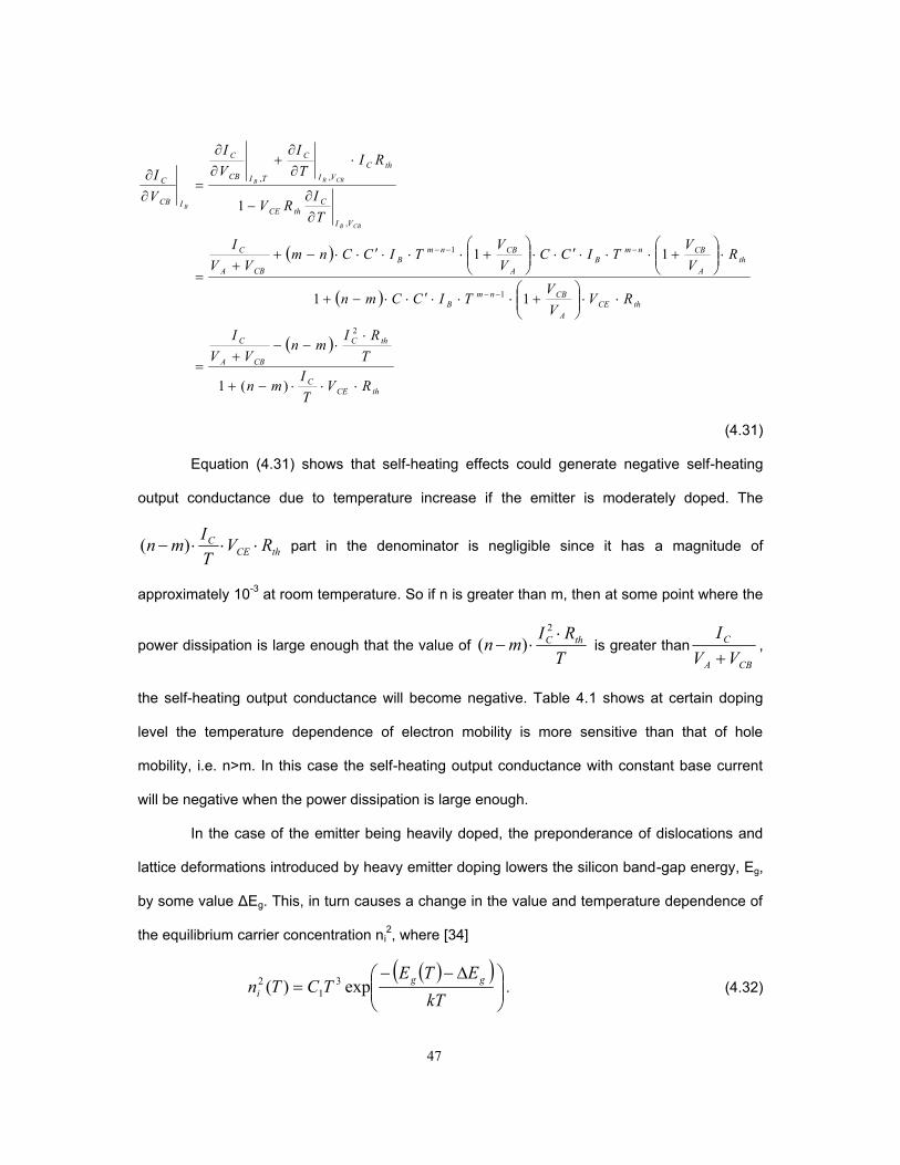
47
thCEC
thC
CBA
C
thCEA
CBnmB
thA
CBnmB
A
CBnmB
CBA
C
VI
CthCE
thCVI
C
TICB
C
ICB
C
RVTI
mn
TRI
mnVV
I
RVVV
TICCmn
RVV
TICCVV
TICCnmVV
I
TI
RV
RITI
VI
VI
CBB
CBBB
B
)(1
11
11
1
2
1
1
,
,,
(4.31)
Equation (4.31) shows that self-heating effects could generate negative self-heating
output conductance due to temperature increase if the emitter is moderately doped. The
thCEC RVTImn )( part in the denominator is negligible since it has a magnitude of
approximately 10-3 at room temperature. So if n is greater than m, then at some point where the
power dissipation is large enough that the value of TRImn thC
2
)( is greater thanCBA
C
VVI
,
the self-heating output conductance will become negative. Table 4.1 shows at certain doping
level the temperature dependence of electron mobility is more sensitive than that of hole
mobility, i.e. n>m. In this case the self-heating output conductance with constant base current
will be negative when the power dissipation is large enough.
In the case of the emitter being heavily doped, the preponderance of dislocations and
lattice deformations introduced by heavy emitter doping lowers the silicon band-gap energy, Eg,
by some value ΔEg. This, in turn causes a change in the value and temperature dependence of
the equilibrium carrier concentration ni2, where [34]
kTETE
TCTn ggi exp)( 3
12 . (4.32)

48
The variable ΔEg can be modeled as [31]
37D17
3 cm 107Nfor eV 107
ln107.18 -Dg
NE
. (4.33)
ΔEg is equal to 49.72 eV when ND= 319 cm 101 - .
Hence equation (4.22) can be modified as follows
A
CBgBCng
A
CBnmBC V
VkT
TEqVCT
kTE
VVTICCI 1
)(expexp1 4
(4.34)
A derivate of IC over temperature with constant IB and VCB now gives
TI
KTE
nm
kTE
VVTICC
KTE
nm
nV
TVVVV
kTTEqV
CT
kTE
VV
KTE
TICC
kTE
VVTICCnm
VV
kTTEqV
CTT
kTE
VVTICC
TTI
Cg
g
A
CBnmB
g
Negligible
T
gBC
A
CBgBCn
g
A
CBgnmB
g
A
CBnmB
VIA
CBgBCn
VI
g
A
CBnmB
VI
C
CBB
CBBCBB
exp1
4)(
1)(
exp
exp1
exp1
1)(
exp
exp1
1
3
1
1
,
4
,,
. (4.35)
Substituting equation (4.28), (4.29) and (4.35) into (4.27) gives BICB
C
VI
assuming heavy emitter
doping as

49
TRI
KTE
mnVV
I
RVTI
KTE
mn
TRI
KTE
mnVV
I
RVkTE
VV
TICCKTE
mn
RIkTE
VV
TICCKTE
nmVV
I
TI
RV
RITI
VI
VI
thCg
CBA
C
thCECg
thCg
CBA
C
thCEg
A
CBnmB
g
thCg
A
CBnmB
g
CBA
C
VI
CthCE
thCVI
C
TICB
C
ICB
C
CBB
CBBB
B
2
2
1
1
,
,,
)(1
exp11
exp1
1
(4.36)
Equation (4.36) shows the self-heating output conductance with constant base current
driven when emitter is heavily doped. The difference between equation (4.31) and equation
(4.36) is ΔEg/kT due to the reduction of band-gap energy when the emitter is heavily doped.
When the emitter doping concentration is 1019 cm-3, ΔEg/kT is approximately 2. With n=1.25
(NB=1*1017 cm-3) and m=0.43 (NE=1*1019 cm-3) as shown in table 4.1. In this case
KTE
mn g is roughly -1.2. Hence the self-heating output conductance with constant base
current will be always positive when the emitter is heavily doped. This is because an emitter
energy-gap reduction of ΔEg causes a positive exponential temperature dependence of collector
current while electron and hole mobility causes a negative power law temperature dependence
of collector current. The exponential temperature dependence dominates.
4.2.4 Large-Signal Behavior of a Constant Base-emitter Voltage Driven BJT Transistor
Equation (4.13) lays the foundation for the analysis of large-signal behavior of a BJT
driven by a constant base-emitter voltage. Since equation (4.13) is a function of temperature,
collector-base voltage and base-emitter voltage, the total differential of IC is

50
BEVTBE
C
VV
CCB
TVCB
CC V
VIT
TIV
VIdI
CBCBBEBE
,,,
. (4.37)
By holding base-emitter voltage constant a self-heating output conductance is
CB
j
VV
C
TVCB
C
VCB
C
VCE
Cosh V
TTI
VI
dVdI
dVdIg
CBBEBEBEBE
,,
. (4.38)
The derivative of the collector current with respect to the temperature CBBE VV
C
TI
,
can be first
solved as
kTEqV
A
CBn
T
CEC
T
gBEC
gBCkTEqV
A
CBn
gBEkTEqV
A
CBn
gBEkTEqV
A
CBn
gBEkTEqV
A
CBn
A
CBkTEqV
kTEqV
n
gBCkTEqV
A
CBn
gBEkTEqV
A
CBn
A
CBkTEqV
kTEqV
nVV
C
gBC
gBC
gBC
gBC
gBE
gBCgBE
gBC
gBE
gBCgBE
CBBE
eVV
CTTV
VI
TVVV
TI
n
kTEqV
eVV
CT
kTEqV
eVV
CT
kTEqV
eVV
CT
kTEqV
eVV
CT
VV
eeTnC
kTEqV
eVV
CT
kTEqV
eVV
CT
VV
eeTnCTI
)0(4
2
)0(4
2
)0(4
2
)0(4
2
)0(4
)0()0(3
2
)0(4
2
)0(4
)0()0(3
,
)1())0((
)4(
))0(()1(
))0(()1(
))0(()1(
))0(()1(
)1()4(
))0(()1(
))0(()1(
)1()4(
(4.39)

51
The derivative of the collector current with respect to the collector-base voltage TVCB
C
BEVI
,
can
be solved as follows
)1(
)1(
)1(
Negligible
)0(4
)0(4)0()0(4
)0(4
)0(4)0(4
,
CBA
C
A
CBkTEqV
T
n
CBA
CT
A
CBkTEqV
T
nkT
EqVkT
EqV
A
n
kTEqV
A
n
kTEqV
A
n
A
CBkTEqV
T
n
VCB
C
VVI
VV
eV
CTVV
IVV
eV
CTeeVCT
eVCT
eVCT
VV
eV
CTVI
gBC
gBCgBCgBE
gBE
gBCgBC
TBE
(4.40)
A derivative of equation (4.1) under constant base-emitter voltage driven circumstance gives
BEVCB
CthCEthC
CB
j
VIRVRI
VT
. (4.41)
Combining equation (4.39), (4.40) and (4.41) into equation (4.38) gives
)1(
))0(()4(1
)1()))0((
4(
1
)0(4
)0(4
2
,
,,
kTEqV
A
CBn
T
CEC
T
gBECthCE
kTEqV
A
CBn
T
CEthC
T
gBEthC
CBA
C
VVC
thCE
VVC
thCVCB
C
VCB
C
gBC
gBC
CBBE
CBBETBE
BE
eVV
CTTV
VI
TVVV
TI
nRV
eVV
CTTVVRI
VVV
nTRI
VVI
TI
RV
TI
RIVI
VI
(4.42)
Since ,0)0(
kTEqV gBC
e so equation (42) can be simplified as

52
T
BEgthC
CBA
C
T
gBECthCE
T
gBEthC
CBA
C
VCB
C
VVV
nTRI
VVI
VVV
nTI
RV
VVV
nTRI
VVI
VI
BE
))0((4
))0(()4(1
))0((4
2
2
(4.43)
where qEV gg )0()0( , and 1))0((
)4(
T
gBECthCE V
VVn
TIRV .
Equation (4.43) describes the self-heating output conductance of a BJT driven by
constant base-emitter voltage. It consists of two parts. The first part, CBA
C
VVI
, represents the
output conductance when VBE and temperature are constant, which results from the Early effect.
The second part results from the self-heating effect. Note that it is related to collector current,
thermal resistance and a constant
T
BEg
VVV
n))0((
4 which has the value of
approximately 14. Since the second part is always positive and much greater than the first part,
the slope of the device output characteristic will be steeper than the results without self-heating
effects considered.
4.3 A Method for Extraction of the Early Voltage and Thermal Resistance
4.3.1 Theory
An output conductance observed in IC-VCE characteristics originates from multiple
sources including the Early effect and the self-heating effect. Since an accurate prediction of
output conductance is desirable for high-power applications, identifying the early voltage and
thermal resistance is important [35].
Equations (4.36) and (4.43) describe the output conductance when the device is driven
by a constant base current or constant base-emitter voltage, respectively. Based on these two
equations, a method for extraction of Early Voltage and thermal resistance is proposed.
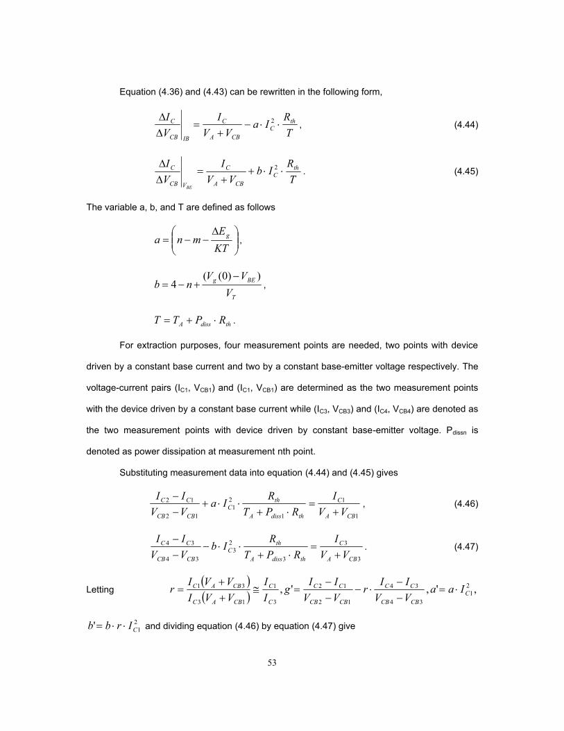
53
Equation (4.36) and (4.43) can be rewritten in the following form,
TRIa
VVI
VI th
CCBA
C
IBCB
C
2 , (4.44)
TRIb
VVI
VI th
CCBA
C
VCB
C
BE
2 . (4.45)
The variable a, b, and T are defined as follows
KTE
mna g ,
T
BEg
VVV
nb))0((
4
,
thdissA RPTT .
For extraction purposes, four measurement points are needed, two points with device
driven by a constant base current and two by a constant base-emitter voltage respectively. The
voltage-current pairs (IC1, VCB1) and (IC1, VCB1) are determined as the two measurement points
with the device driven by a constant base current while (IC3, VCB3) and (IC4, VCB4) are denoted as
the two measurement points with device driven by constant base-emitter voltage. Pdissn is
denoted as power dissipation at measurement nth point.
Substituting measurement data into equation (4.44) and (4.45) gives
1
1
1
21
12
12
CBA
C
thdissA
thC
CBCB
CC
VVI
RPTRIa
VVII
, (4.46)
3
3
3
23
34
34
CBA
C
thdissA
thC
CBCB
CC
VVI
RPTRIb
VVII
. (4.47)
Letting ,',', 2
134
34
12
12
3
1
13
31C
CBCB
CC
CBCB
CC
C
C
CBAC
CBAC IaaVVIIr
VVIIg
II
VVIVVIr
21' CIrbb and dividing equation (4.46) by equation (4.47) give

54
02 CRBRA thth . (4.48)
The variable A, B and C are defined as follows,
1331 ''' dissdissdissdiss PbPaPPgA ,
AdissdissA TbaPPTgB ''' 31 ,
2' ATgC .
The thermal resistance, Rth, can be obtained by solving the quadratic equation (4.48), and
hence the Early voltage VA can be obtained.
4.3.2 Parameters Mapping
For an unknown device, it is necessary to map the values of the variables, a and b, to
the VBIC model parameters. The temperature dependence of the transport saturation current in
the VBIC model is [5]
FN
nom
XIS
nomnomSS T
TkTEAq
TTTITI
1
1exp)()(
. (4.49)
Thus the temperature coefficient of collect current below knee current, IKF with the reverse
transport current neglected is
)()(TF
BE
T
CCC VN
VVEAXIS
TI
TIITC
. (4.50)
Comparing this result to equation (4.45) gives
TF
BE
T VNV
VEAXISb
. (4.51)
The intrinsic ideal base-emitter saturation current, Ibei, varies with temperature as [5]
EIN
nom
XII
nomnombeibei T
TkTEAIEq
TTTITI
1
2
1exp)()(
. (4.52)
Thus the temperature coefficient of current gain over most of the mid current region with non-
ideal base-emitter saturation current, Iben, neglected is
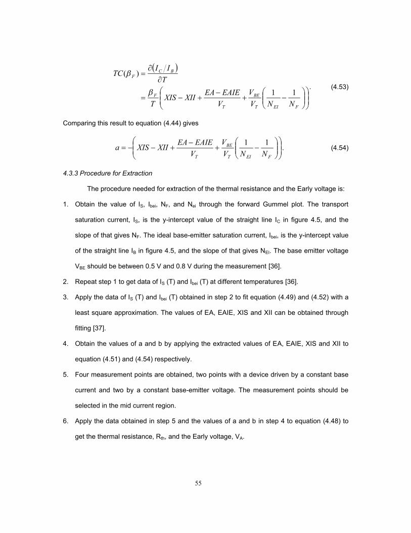
55
FEIT
BE
T
F
BCF
NNVV
VEAIEEAXIIXIS
T
TIITC
11
)(
. (4.53)
Comparing this result to equation (4.44) gives
FEIT
BE
T NNVV
VEAIEEAXIIXISa 11
. (4.54)
4.3.3 Procedure for Extraction
The procedure needed for extraction of the thermal resistance and the Early voltage is:
1. Obtain the value of IS, Ibei, NF, and Nei through the forward Gummel plot. The transport
saturation current, IS, is the y-intercept value of the straight line IC in figure 4.5, and the
slope of that gives NF. The ideal base-emitter saturation current, Ibei, is the y-intercept value
of the straight line IB in figure 4.5, and the slope of that gives NEI. The base emitter voltage
VBE should be between 0.5 V and 0.8 V during the measurement [36].
2. Repeat step 1 to get data of IS (T) and Ibei (T) at different temperatures [36].
3. Apply the data of IS (T) and Ibei (T) obtained in step 2 to fit equation (4.49) and (4.52) with a
least square approximation. The values of EA, EAIE, XIS and XII can be obtained through
fitting [37].
4. Obtain the values of a and b by applying the extracted values of EA, EAIE, XIS and XII to
equation (4.51) and (4.54) respectively.
5. Four measurement points are obtained, two points with a device driven by a constant base
current and two by a constant base-emitter voltage. The measurement points should be
selected in the mid current region.
6. Apply the data obtained in step 5 and the values of a and b in step 4 to equation (4.48) to
get the thermal resistance, Rth, and the Early voltage, VA.

56
Figure 4.5 Forward Gummel plot
4.3.4 Simulation Results
Figure 4.6 shows the forward Gummel plot of the NPN transistor with the ambient
temperature at 298 K. Figure 4.7 shows the variation of the transport saturation current with
temperature. The circle represents the extracted IS through the forward Gummel plot at different
temperatures. The solid line represents fitting the data to equation (4.49) with the nominal
temperature at 298 K. Figure 4.8 shows the variation of the ideal base-emitter saturation current
with temperature. The circle represents the extracted Ibei data from the forward Gummel plot at
different temperatures. The solid line represents fitting the data to equation (4.52) with the
nominal temperature at 298K. Table 4.2 summarizes the values of a and b obtained through the
extracted VBIC parameters and compares these to the values of a and b obtained via the VBIC
model parameters attached in Appendix A.
Figure 4.9 shows the DC response with IB=2 μA and TA=298 K, and figure 4.10 shows
the DC response with VBE=819.1 mV and TA=298 K. Four simulation points are obtained from
figure 4.9 and figure 4.10. By applying the data of the four simulation points into equation (4.49),
a thermal resistance value Rth=2908 is obtained compared to the thermal resistance value
Rth=3000 in the model parameters. Thereby an Early voltage value, VA=141, is obtained
comparable to the Early voltage value VA=156 in the model parameters.
Table 4.3 shows the variation of the thermal resistance, Rth, and the Early voltage, VA,
with the collector-emitter voltage, VCE. It is seen that around VCE=1.7 V, the extracted value of

57
Rth and VA approach the real model value most. This is because the VBIC models the quasi-
saturation effect and the Early voltage, VA, models the critical point where the operating mode of
transistor transfers from saturation to forward-active.
Table 4.2 Extracted parameters
Extracted Model XIS 5.9973 5.75 XII 3.0001 3.77 EA (eV) 1.1127 1.3 EAIE (eV) 1.1257 1.2 NF 0.999 1 NEI 1.021 1 a -2.49 -2.36 b 17.35 17.77
0.2 0.3 0.4 0.5 0.6 0.7 0.8
-12
-10
-8
-6
-4
-2
0
VBE and VCE (V)
logI
C and
logI
B (AM
PS
)
Collector currentBase current
Figure 4.6 Forward Gummel plot with TA=298 K
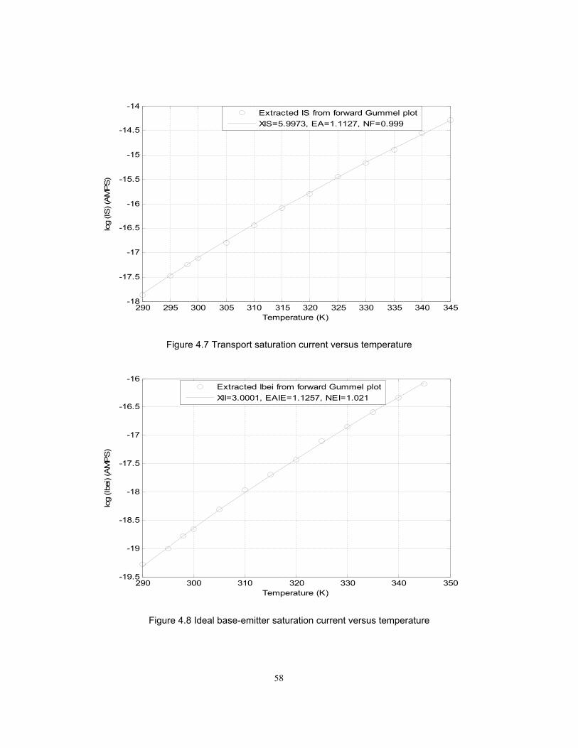
58
290 295 300 305 310 315 320 325 330 335 340 345-18
-17.5
-17
-16.5
-16
-15.5
-15
-14.5
-14
Temperature (K)
log
(IS) (
AM
PS
)Extracted IS from forward Gummel plotXIS=5.9973, EA=1.1127, NF=0.999
Figure 4.7 Transport saturation current versus temperature
290 300 310 320 330 340 350-19.5
-19
-18.5
-18
-17.5
-17
-16.5
-16
Temperature (K)
log
(Ibei
) (A
MP
S)
Extracted Ibei from forward Gummel plotXII=3.0001, EAIE=1.1257, NEI=1.021
Figure 4.8 Ideal base-emitter saturation current versus temperature

59
0 0.5 1 1.5 2 2.5 3 3.5 4 4.5 50
20
40
60
80
100
120
140
160
180
VCE (V)
I C ( A)
(1.0,156.19) (3.0,159.59)
Figure 4.9 DC Response with constant IB=2 μA, TA=298K
0 0.5 1 1.5 2 2.5 3 3.5 4 4.5 50
50
100
150
200
250
300
VCE (V)
I C ( A)
(1.0,225.24)(3.0,245.58)
Figure 4.10 DC Response with constant VBE=819.1 mV, TA=298K
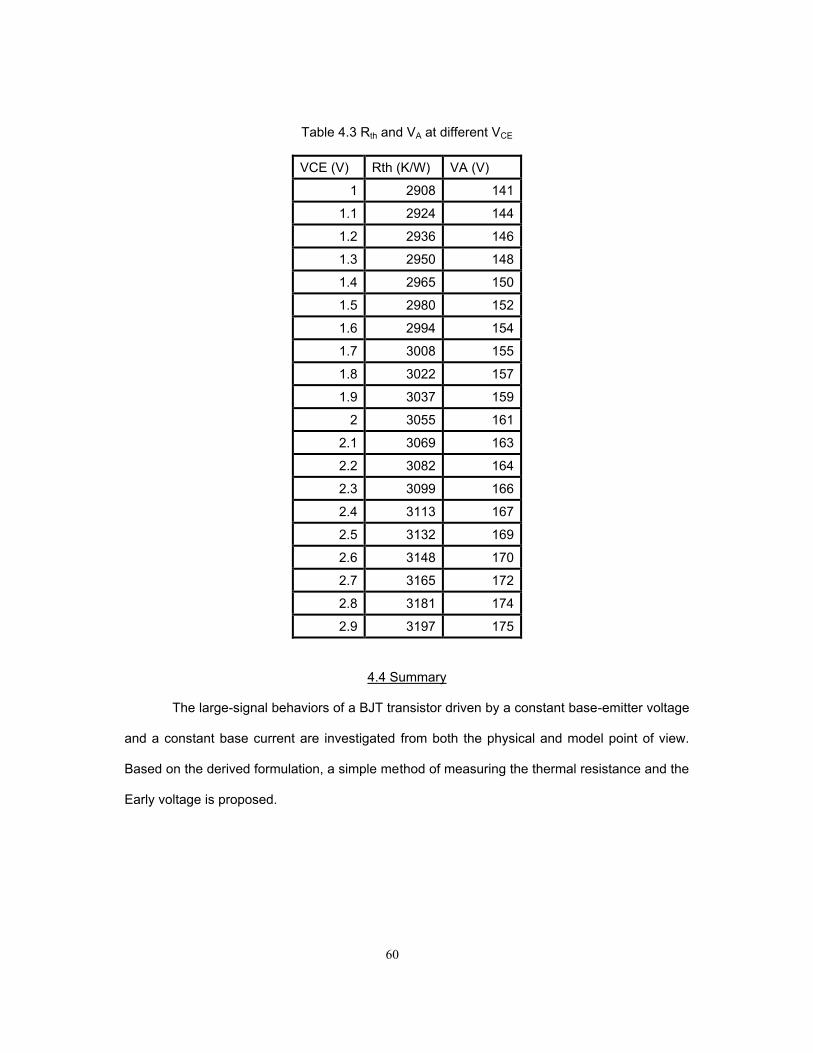
60
Table 4.3 Rth and VA at different VCE
VCE (V) Rth (K/W) VA (V)
1 2908 141
1.1 2924 144
1.2 2936 146
1.3 2950 148
1.4 2965 150
1.5 2980 152
1.6 2994 154
1.7 3008 155
1.8 3022 157
1.9 3037 159
2 3055 161
2.1 3069 163
2.2 3082 164
2.3 3099 166
2.4 3113 167
2.5 3132 169
2.6 3148 170
2.7 3165 172
2.8 3181 174
2.9 3197 175
4.4 Summary
The large-signal behaviors of a BJT transistor driven by a constant base-emitter voltage
and a constant base current are investigated from both the physical and model point of view.
Based on the derived formulation, a simple method of measuring the thermal resistance and the
Early voltage is proposed.
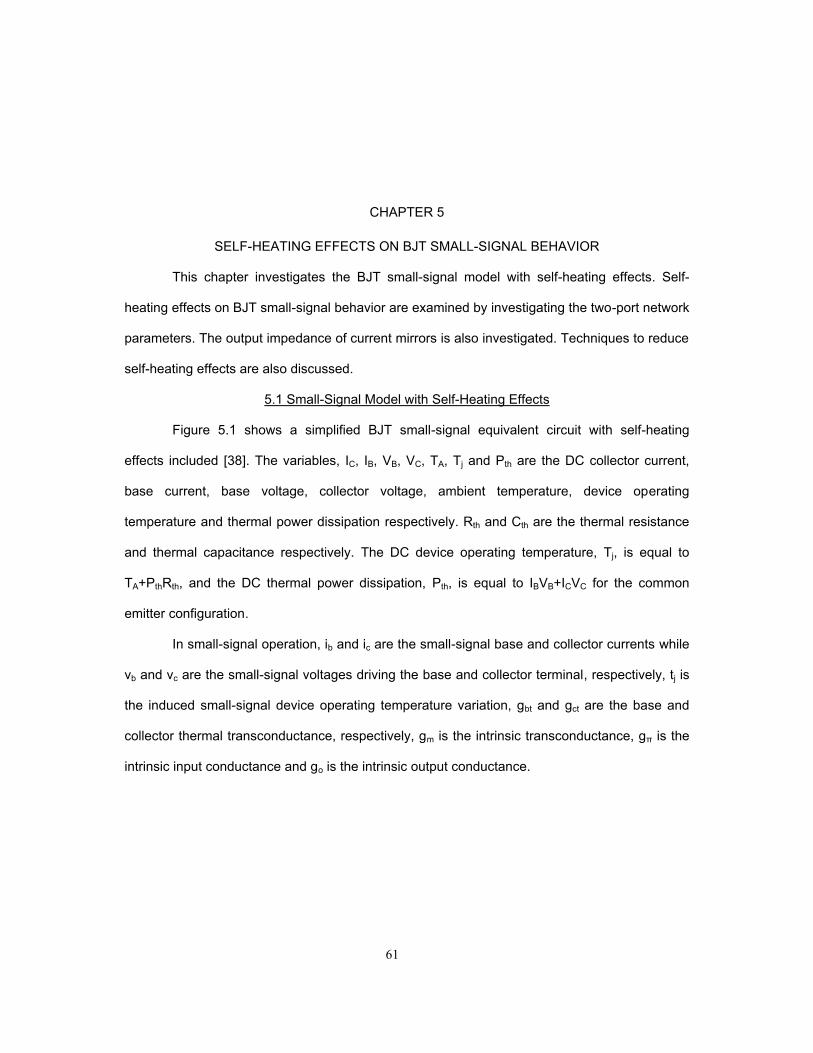
61
CHAPTER 5
SELF-HEATING EFFECTS ON BJT SMALL-SIGNAL BEHAVIOR
This chapter investigates the BJT small-signal model with self-heating effects. Self-
heating effects on BJT small-signal behavior are examined by investigating the two-port network
parameters. The output impedance of current mirrors is also investigated. Techniques to reduce
self-heating effects are also discussed.
5.1 Small-Signal Model with Self-Heating Effects
Figure 5.1 shows a simplified BJT small-signal equivalent circuit with self-heating
effects included [38]. The variables, IC, IB, VB, VC, TA, Tj and Pth are the DC collector current,
base current, base voltage, collector voltage, ambient temperature, device operating
temperature and thermal power dissipation respectively. Rth and Cth are the thermal resistance
and thermal capacitance respectively. The DC device operating temperature, Tj, is equal to
TA+PthRth, and the DC thermal power dissipation, Pth, is equal to IBVB+ICVC for the common
emitter configuration.
In small-signal operation, ib and ic are the small-signal base and collector currents while
vb and vc are the small-signal voltages driving the base and collector terminal, respectively, tj is
the induced small-signal device operating temperature variation, gbt and gct are the base and
collector thermal transconductance, respectively, gm is the intrinsic transconductance, gπ is the
intrinsic input conductance and go is the intrinsic output conductance.

62
b c
th
j
A
j
A
C
B
CB
c
b
Figure 5.1 Simplified BJT small-signal equivalent circuit with self-heating effects included [38]
The Kirchhoff’s Current Law (KCL) is applied to the at base and collector terminal,
jbtcbb tgvsCvCCsgi , (5.1)
jctcCSobmc tgvCCsgvsCgi , (5.2)
where B
B
VIg
, C
Co V
Ig
, B
Cm V
Ig
, j
Bbt T
Ig
and j
Cct T
Ig
.
The induced small-signal power dissipation variation, dPth, is
bBBbcCCcth vIVivIVidP . (5.3)
Therefore the induced small-signal device operating temperature variation, tj, can be expressed
as
thbBBbcCCcj ZvIVivIVit (5.4)
where the thermal impedance, Zth (s), is equal to ththth CsRR 1 .
Substituting equation (5.1) and (5.2) into equation (5.4) gives

63
jBbtCctbCmBBcCoCthj tVgVgvVgVgIvVgIYt . (5.5)
Here the variable, Yth, is the thermal admittance and is the reciprocal of the thermal impedance.
Therefore the small-signal device operating temperature variation, tj, is [38]
BbtCctth
bCmBBcCoCj VgVgY
vVgVgIvVgIt
. (5.6)
The small-signal equivalent circuit with self-heating effects included in figure 5.1 can be
simplified as a two-port equivalent circuit in figure 5.2 where i1=ib, i2=ic, v1=vb and v2=vc. The
parameters, y11, y12, y21 and y22, can be found and interpreted as follows: 01
111
2
vv
iy is the
input admittance with the output short-circuited, 02
112
1
vv
iy is the reverse transconductance
with the input short-circuited, 01
221
2
vv
iy is the forward transconductance with the output
short circuited and 02
222
1
vv
iy is the output admittance with the input short circuited [33].
Figure 5.2 Admittance-parameter, two-port equivalent circuit [33].
By applying the above parameters definition and substituting equation (5.6) into
equation (5.1) and (5.2), the small-admittance parameters with self-heating effects included are
thus obtained as follows: [38]

64
)()(
)(11
CCs
VgVgYVgVgIggsyBbtCctth
CmBBbt
, (5.7)
sCVgVgY
VgIgsyBbtCctth
CoCbt
)()(
12 , (5.8)
sC
VgVgYVgVgIggsyBbtCctth
CmBBctm
)(
)(21 (5.9)
)()(
)(22 CS
BbtCctth
CoCcto CCs
VgVgYVgIggsy
(5.10)
Note that by neglecting gbtVB and substituting equation (4.39) and equation (4.40) for gct and go
respectively, the DC output admittance with self-heating in equation (5.10) agrees with the
large-signal output conductance with self-heating in equation (4.43). It should be also noted
from equation (5.10) that the output admittance is composed of two components. One is the
intrinsic component, i.e. )( CSo CCsg , the other is the thermal induced component, i.e.
)()(
BbtCctth
CoCct
VgVgYVgIg
. The output admittance tends to decrease with frequency until the effect
of thermal capacitance dominates the thermal induced component. After that, the output
admittance will be dominated by the intrinsic component. This behavior can be also explained
by the following pole-zero analysis of the output impedance.
The output impedance with self-heating included when the input is short circuited can
be obtained by using equation (5.10) as [39]
1
11
1
11
11
)(1
2220
sRXMRgMRCgCR
sRXMRg
CCRCRMR
sMRRXg
sysZ
thgtho
theqothth
thgtho
eqthth
thththththgovoin
(5.11)
where M=gctVC+gbtVB, Xg=gct(IC+goVC), and Ceq=Cμ+CCS. Assuming MRth <<1 and RthCthgo>>Ceq,
a left half plane (LHP) zero and two LHP poles can be identified as [39]

65
ththth CR
MRz 1)1( , (5.12)
eq
thth
eqthgooo
CCR
CRXggg
p2
42
2,1
. (5.13)
By using Taylor series expansion of the square root function, i.e. 211 xx and
assuming (go+XgRth)Ceq<<go2RthCth, the two poles can be further simplified as
ththo
thgo
CRgRXg
p 11
, (5.14)
eq
o
Cgp 2 . (5.15)
Figure 5.3 Poles and zero of the output impedance with self-heating included.
It can be inferred from equation (5.12) and (5.14) that the LHP thermal induced zero precedes
the thermal induced LHP pole, and the intrinsic pole of the device positions leftmost as in figure
5.3. Thus the magnitude of the output impedance begins to increase at 20 dB/decade at f=fz,
becomes flat at f=fp1, and then begins to drop at 20 dB/decade at f=fp2.
The frequency response behavior of the output impedance can affect the gain of
amplifier significantly. Figure 5.4 shows a common-emitter amplifier with a current source load
driven by a voltage source. The output impedance response behavior dominates the gain

66
response of the amplifier as shown in figure 5.5. The gain magnitude starts to increase around
fz≈31.6 KHz at 20 dB/decade and begins to drop around fp2≈12.6 MHz.
It is clear that techniques that raise the effective output impedance can reduce error
due to self-heating. On the one hand, raising the effective output impedance can make the
intrinsic component of the output impedance dominate in magnitude; on the other hand, it can
also make the intrinsic pole closer to the thermal induced zero and pole pair that the frequency
response will be more flat. These techniques include cascoding and negative feedback as with
Wilson current mirrors or emitter degeneration [26].
Figure 5.4 A common-emitter amplifier with a current source load driven by a voltage source.

67
100
102
104
106
108
1010
0
10
20
30
40
50
60
70
80
Frequency (Hz)
Gai
n m
agni
tude
(dB
)
without self-heatingwith self-heating
Figure 5.5 The gain magnitude of the amplifier shown in figure 5.4.
5.2 Self-heating Effects on the Output Impedance of a Current Mirror
Current mirrors are widely used in analog integrated circuits both as biasing elements
and as loads for amplifier stages. When used as a load in amplifiers, the high output impedance
of current mirrors results in high voltage gain at low-supply voltages. This section investigates
self-heating effects on the output impedance of current mirrors.
The simplest form of a current mirror, which composed of two transistors, is shown in
figure 5.6. The output resistance of the current mirror without self-heating in the forward-active
region is ro=VA ∕ Ibias [33]. Neglecting the resistance looking into the base of Q1, the output
impedance of the current mirror can be approximated using equation (5.11). The location of the
zero and the two poles can be obtained via equation (5.12), (5.14) and (5.15). Thus the
magnitude of the output impedance begins to increase at 20 dB/decade at f=fz, becomes flat at
f=fp1, and then begins to drop at 20 dB/decade at f=fp2.
The frequency response of the output impedance of the simple current mirror of figure
5.6 using the VBIC model in appendix A is shown in figure 5.7. The area of the transistors used

68
in the simulation is 8x5 μm2, Ibias=200 μA, Vcc=5V and Vo=5V. In the low frequency region, the
thermal induced conductance is significant that the output resistance of the simple current
mirror with self-heating is approximately 60% of the one without self-heating. As frequency
increases up to the thermal induced zero, the thermal induced conductance begins to decrease,
thus the output resistance of the simple current mirror continues to increase until the frequency
reaches the thermal induced pole, fp1. The output resistance becomes flat. As the frequency
reaches the intrinsic pole, fp2, the output resistance of the simple current mirror begins to drop.
Figure 5.6 A simple current mirror and its output impedance simulation configuration.
100
102
104
106
108
1010
0
100
200
300
400
500
600
700
800
900
1000
Frequency (Hz)
Z o (kOhm
s)
without self-heatingwith self-heating
Figure 5.7 The magnitude of the output impedance of the simple current mirror in figure 5.6.

69
Raising the effective output impedance is an effective approach to reduce error in the
current mirror. The cascode current mirror shown in figure 5.8 offers a very high output
resistance. The output resistance of the cascode current mirror is approximately βro4/2 where β
is the current gain [33].
The output admittance of the cascade current mirror can be approximated as [39]
.
14
424
4
4244
444422
thbbtcct
thcoc
oom
ctbtomct
oom
oomo
ZVgVgZVgI
ggggggggg
sCgggg
ggggy
(5.16)
Assuming gm+go4>>go2+gπ4, equation (5.16) can be simplified as
thbbtcct
thcocbt
oom
oomo ZVgVg
ZVgIgsCgggg
ggggy
1
4
4244
444422
. (5.17)
Because gbt is generally 1/20 of gct, it is cleared that the thermal induced admittance is greatly
suppressed by comparing equation (5.17) to equation (5.10). At the same time, the intrinsic
admittance is greatly reduced by cascoding transistors.
The frequency response of the output impedance of the cascode current mirror of
figure 5.8 is shown in figure 5.9. The VBIC model in appendix A is used in this simulation. The
area of the transistors is 8x5 μm2, Ibias=200 μA, Vcc=5V and Vo=5V. As shown in figure 5.9, the
low frequency error is suppressed in cascode current mirror at the expense of bandwidth and
the output resistance of the cascode current mirror without self-heating is slightly higher than
without self-heating.

70
Figure 5.8 Cascode current mirror and its output impedance simulation configuration.
100
102
104
106
108
1010
0
5
10
15
20
25
30
35
40
Frequency (Hz)
Z o (kO
hms)
with self-heatingwithout self-heating
Figure 5.9 The magnitude of the output impedance of the cascode current mirror in figure 5.8.
Another technique to raising the effective output impedance is using negative feedback.
The Wilson current mirror is shown in figure 5.10. The Wilson current mirror uses negative
feedback through Q2, activating Q1 to reduce the base-current error and raising the output

71
resistance. The output resistance of the Wilson current mirror without self-heating can be
approximated as βro3/2 which is the same as the cascode current mirror [33].
The frequency response of the output impedance of the Wilson current mirror of figure
5.10 is shown in figure 5.11. The VBIC model in appendix A is used in this simulation. The area
of the transistors is 8x5 μm2, Ibias=200 μA, Vcc=5V and Vo=5V. As shown in figure 5.11, the
output resistance of the Wilson current mirror displays the same characteristic as the cascode
current mirror.
CC
1 2
3
bias
o o
o o o o
Figure 5.10 Wilson current mirror and its output impedance simulation configuration.
100 102 104 106 108 10100
5
10
15
20
25
30
35
Frequency (Hz)
Z o (kOhm
s)
with self-heatingwithout self-heating
Figure 5.11 The magnitude of the output impedance of the Wilson current mirror in figure 5.10.

72
5.3 Summary
The self-heating effects on the small-signal behavior of a BJT are discussed. The
output impedance of a BJT with self-heating displays serious reduction at low frequency due to
thermal induced zero and poles. Gain of amplifiers is reduced at low frequency. Techniques that
raise the output resistance can reduce such errors, i.e. cascoding, negative feedback as with
the Wilson current mirrors, or emitter degeneration.

73
CHAPTER 6
THE EFFECT OF SELF-HEATING IN TRANSIENT OPERATION
Errors caused by self-heating effects in transient operation can be substantial,
especially for some switching circuits. In switching circuits the change of device operating
temperature causes a change in the the base-emitter voltage which consequently a thermal tail
in the output of the transistor. The change of device operating temperature is an exponentially
increasing function of time with a time constant equal to the product of the thermal resistance
and the thermal capacitance. Therefore, the settling time of switching circuits can be
significantly degraded by self-heating since thermal transients take a much longer time to settle.
This chapter investigates the effect of self-heating on the transient operation and applies it to
the operation analysis of a high speed voltage buffer.
6.1 Time Dependent Device Temperature
The change in device temperature, ΔT=Tj-TA, can be described in terms of the power
dissipation in the device, Pth, thermal resistance, Rth, thermal capacitance, Cth, and ambient
temperature, TA, by the electro-thermal model in figure 6.1:
0
thth
th PRT
dtTdC . (6.1)
The solution for ΔT in equation (6.1) is an exponentially increasing function of time with a time
constant, τth=RthCth, and an asymptotic value of PthRth. It is in the following form [1]:
ththth
tRPT
exp1 . (6.2)
Equation (6.2) shows that the change in device temperature varies with time, and reaches the
asymptotic value of PthRth after a time delay of about five times the time constant τth. Figure 6.2
shows a typical curve of variation of the change in device temperature with time in a transient

74
operation. Because of the device temperature change with time, the collector current and the
base-emitter voltage (VBE) will also change with time. Figure 6.3 shows a typical curve of the
variation of voltage with time in transient operation.
thth
A
j
th
j
A
C
E
E
CB
B
Figure 6.1 Electro-thermal model of BJT.
0 5 10 15 20 25 30 35 400
0.5
1
1.5
2
2.5
Time (s)
Cha
nge
in D
evic
e Te
mpe
ratu
re (K
)
Figure 6.2 Typical curve of variation of the change in device temperature with time.

75
t
Voltage
Without self-heating
With self-heating
thermal tail
thermal tail
Thermal constant τth
Low to High Transition
High to Low Transition
V1
V2
Figure 6.3 Typical curve of the variation of voltage with time.
6.2 Self-Heating on Collector Current
In bipolar devices, collector current is a function of VBE (base-emitter voltage), VCE
(Collector-emitter voltage) and device operating temperature. For a constant base-emitter
voltage driven BJT device, the collector current can be represented as a second order, two –
dimensional Taylor series expansion:
CEjCE
CCE
TCE
Cj
V
C
CETCE
Cj
V
C
CEACCECEjAC
VTVTI
VVI
TTI
VVI
TTI
VTIVVTTI
ACE
ACE
22
2
22
2
2
221
(6.3)
),(),(
where TA is the ambient temperature, jT is the change of device operating temperature
because of self-heating, TIC
and 2
2
TIC
are the first and second order temperature derivative
of collector current respectively, CE
C
VI
and 2
2
CE
C
VI
are the first and second order collector-

76
emitter voltage derivative of collector current respectively and CE
C
VTI2
is the second order
cross derivative of collector current.
Figure 6.4 shows a transistor biased with a constant base emitter voltage, VBE and a
collector-emitter voltage, VCE. With collector-emitter voltage increasing from VCE to VCE+ΔVCE,
the increasing power dissipation will increase the device operating temperature. Here the base-
emitter voltage, VBE, is 819.1 mV, the collector-emitter voltage, VCE, is 4.15 V, the change in
collector-emitter voltage, ΔVCE, is 1 V, and the ambient temperature, TA, is 27 °C. Figures 6.5
and 6.6 show the variations of the first and second order temperature derivative of collector
current with temperature when VBE=819.1 mV and VCE=4.15 V, and the first and second order
temperature derivative are 9.31 μA/K, 0.313 μA/K2 respectively at 27 °C. Figures 6.7 and 6.8
show the variations of the first and second order collector-emitter voltage derivative of collector
current with collector-emitter voltage when VBE=819.1 mV and TA=27 °C, and first and second
order collector-emitter voltage derivative are 1.13 μA/V, -0.0491 μA/V2 respectively when
VCE=4.15 V. The SPECTRE simulator is used here to get these curves.
The change of device operating temperature from the ambient temperature can be
expressed as:
thCECEjACCECEj RVVTTIVVT ),()( (6.4)
Substituting equation (6.3) into equation (6.4) and solving a quadratic equation about jT gives
jT =3.665 C. Thus collector current after a change in collector-emitter voltage change can be
expressed as

77
A 20.237
2!2
1
),(),(
05.0
22
2
374.0
2
20.4
22
2
125.114.34
7.199
CETCE
CCEj
CE
Cj
V
C
CETCE
C
V
CCEACCECEjAC
VVI
VTVTI
TTI
VVI
TTI
VTIVVTTI
ACE
ACE
Figure 6.9 shows how collector current varies with collector-emitter voltage with and
without self-heating effects. The simulation result agrees well with the analytical result. It can be
seen that the second order dependence of collector current on the collector-emitter voltage and
the cross term are negligible. By considering the first order dependence of collector current on
temperature and the collector-emitter voltage, the collector current of a BJT driven by fixed
base-emitter voltage with self-heating effect can be roughly estimated.
Figure 6.4 A biased BJT with collector-emitter voltage changing.

78
26 26.5 27 27.5 28 28.5 29 29.5 308.8
9
9.2
9.4
9.6
9.8
10
10.2
10.4
Temperature (C)
IC/
T (1
0-6)
(27,9.31)
Figure 6.5 First order temperature derivative of collector current with
VBE=819.1 mV and VCE=4.15 V.
26 26.5 27 27.5 28 28.5 29 29.5 303.08
3.1
3.12
3.14
3.16
3.18
3.2
3.22
3.24
Temperature (C)
2 I C/ T2 (1
0-7)
(27,3.13)
Figure 6.6 Second order temperature derivative of collector current with
VBE=819.1 mV and VCE=4.15 V.

79
3 3.2 3.4 3.6 3.8 4 4.2 4.4 4.6 4.8 50
0.2
0.4
0.6
0.8
1
1.2
1.4
1.6
1.8
2
VCE (V)
IC/
VCE
(10-6
)
(4.1,1.13)
Figure 6.7 First order collector-emitter voltage derivative of collector current with
VBE=819.1 mV and TA=27 C.
3 3.2 3.4 3.6 3.8 4 4.2 4.4 4.6 4.8 5-8
-7.5
-7
-6.5
-6
-5.5
-5
-4.5
-4
-3.5
VCE (V)
2 I C/ V
CE2 (1
0-8)
(4.1,-4.91)
Figure 6.8 Second order collector-emitter voltage derivative of collector current with
VBE=819.1 mV and TA=27 C.

80
3 3.5 4 4.5 5 5.5 6190
200
210
220
230
240
250
VCE (V)
I C ( A)
(5.15,237.20)
(4.15,199.7)
with self-heatingwithout self-heating
Figure 6.9 Variation of collector current with VCE when with and without self-heating effects,
VBE=819.1 mV and TA=27 C.
6.3 Temperature Effect on the Base-Emitter Voltage
The temperature coefficient of the base-emitter voltage is a function of collector current
and temperature. The collector current can be expressed as [29]
qkTVV
TCI gBEnC
)0(exp4 (6.5)
where q is the electronic charge, k is Boltzmann’s constant, C is an empirical constant, the
band-gap voltage at 0 K, )0(gV , is equal to qEg )0( and n is the mobility exponent for
nTT 00 . Solving for VBE gives
nCTgBE TCIVVV 4ln)0( (6.6)
Therefore the temperature coefficient of the base-emitter voltage at a fixed collector current can
be approximated as [29]
nC
I
BE
TCI
qkn
qk
TV
C
4ln4 (6.7)

81
Figure 6.10 shows the variation of the base-emitter voltage with temperature for NPN and PNP
transistors used in the dissertation at 200 μA. The temperature coefficients of the base-emitter
voltages for NPN and PNP transistors are -1.45 mV/°C and -1.3 mV/°C respectively.
24 26 28 30815
816
817
818
819
820
821
822
823
Temperature (oC)
VBE
npn (m
V)
slope=-1.45
24 26 28 30845
846
847
848
849
850
851
852
Temperature (oC)
VBE
pnp (m
V)
slope=-1.3
Figure 6.10 The variation of the base-emitter voltage with temperature for NPN and PNP
transistors at 200 μA
6.4 Self-Heating on Transient Operation of Voltage Buffer
6.4.1 Voltage Buffer Biased with an Ideal Current Source
Figure 6.11 shows a voltage buffer biased with an ideal constant current source. Since
the input voltage switches from low to high, the power dissipation of the transistor Q2 decreases
because of the decrease of the collector-emitter voltage of Q2. Hence the device operating
temperature of Q2 decreases. Consequently, the base-emitter voltage of Q2 increases with
device operating temperature decreasing, and the collector current of Q2 will also reflect the
change of the base-emitter voltage and the device operating temperature.

82
VEE
VCC
2
oin
dT
200µA
200µA
Q
Q
4
1
3
Figure 6.11 Voltage buffer biased with ideal constant current source.
There are three important times to be considered:
1. The time just before the input step occurs is t=0-, or t=0-δ. At this time, the static self-
heating effect before the input step is applied. The notation CRthI denotes the change in
collector current resulting from self-heating to the collector current when self-heating is
ignored, i.e. )0,0()finite,0( thCthCCRthRtIRtII , where the symbol
Rth
is an abbreviation for “change in because of static self-heating effect”.
2. The time, t=0+, or t=0+δ. At this time, the Early effect caused by the change in the collector-
emitter voltage is applied. The notation CEI denotes the change in collector current due to
the Early effect caused by the change in the collector-emitter voltage, where the symbol E
is an abbreviation for “change in because of the Early effect”.
3. The circuit response reaches equilibrium at t>>5τth. The dynamic self-heating effect, i.e. the
change of power dissipation after the input step is applied at this time. The notation CVinI
denotes the change in collector current due to the change of power dissipation caused by
the input step, where the symbol Vin is an abbreviation for “change in because of the power

83
dissipation”. For simplicity purpose, t=final is used to represent this time.
After the input voltage, Vin, steps from 0 to 1, the device operating temperature of
transistor Q2 varies with time ignoring the Early effect as,
)()0()0( 222 tTtTtT QVinjQjQ , (6.8)
)1()0()( 22
222thQthQ CR
t
QthCQinQVineRtIVtT
. (6.9)
As a result the base-emitter voltage of Q2 varies with time as:
)()0( 2)0(
22
tTTVtV QVin
tI
BEBEQVin
CQ
(6.10)
where )0(2
tI
BE
CQTV
is the base-emitter voltage temperature coefficient at fixed collector
current )0(2 tICQ .
The collector current of Q2 after the input step can be found using Kirchhoff’s Voltage
Law (KVL) around translinear loop composed of transistors Q1 through Q4 as:
)()0(
)(
exp)0(
)(
)0(
)(
exp)0(
)0()0(exp
)()0(
)()0()0(exp
)()0(
)0()0(exp)0(
2)0(2
2)0(
2
2)0(
2
2)0(
)0(
2
2)0(
2
2)0(
2
2
2
2
2
2
2
2
tTTI
qtkT
tTTV
tI
tTTI
qtkT
tTTV
qtkT
tVtVI
tTTI
tV
tVtVtVI
tTTI
tVtVtV
ItI
QVintI
C
jQ
QVintI
BE
CQ
QVintI
C
jQ
QVintI
BE
tI
jQ
NPQ
QVintI
C
T
BEQVinNP
Q
QVintI
C
T
NPQCQ
CQ
CQ
CQ
CQ
CQ
CQ
(6.11)
84
If kq
TV
tI
BE
CQ
)0(2
, and the exponential function is expanded as a Taylor series to the
second order, taking into account the Early effect, equation (6.11) becomes
intICE
VintI
C
jQ
QVin
jQ
QVinCQCQ
VVItT
TI
tT
tT
tT
tTtItI
CQCQ
)0(2
)0(
2
2
2
2
2
22
22
)(
)0(
)(
21
)0(
)(1)0()0(
. (6.12)
Equation (6.12) describes the variation of collector current of Q2 with time after the input
step. The first term in equation (6.12) addresses the effect of the base-emitter change with
device operating temperature on collector current, the second term describes the direct effect of
device temperature change on collector current, and the third term deals with the Early effect.
The power transistors Q2 and Q4 have different temperature coefficients of the collector
current and the base-emitter voltage because NPN and PNP transistors mismatch. Therefore
the thermal tail magnitude of the collector current of Q2’s and Q4’s is different, as is the base-
emitter voltage. The base-emitter voltages of Q2’s and Q4’s are then corrected to satisfy the KVL
around the translinear loop and the Kirchhoff’s Current Law (KCL) at the Vo node.
A few variables are to be defined here before further discussion. The magnitude of
thermal tail of the corrected base-emitter voltage is
)0t()finalt( ,,, CBECBECBEVinVVV (6.13)
where the subscript C stands for the corrected. The magnitude of thermal tail of the corrected
collector current is
)0t()finalt( ,,, CCCCCCVinIII . (6.14)
Substituting equation (6.12) and (6.13) into equation (6.14) while ignoring the second order
effect gives

85
CBEVinmVinctCCVinVgTgI ,, (6.15)
where )0(2
tI
Cct T
Ig ,
0tT
Cm V
Ig and thCinVinRtIVT )0( .
The KCL at node Vo requires that the thermal tail magnitude of the collector current of
Q2 and Q4 be the same assuming β2=β4. This gives
CEBQVinQmQVinQctCBEQVinQmQVinQct VgTgVgTg ,44,44,,22,22, . (6.16)
The KVL around the translinear loop requires that
CEBQVinCBEQVinCEBQVinCBEQVinVVVV ,3,1,4,2 . (6.17)
Since Q1 and Q3 are biased with ideal constant current sources in figure 6.11 and the change of
power dissipation is small because of the diode connection, the base-emitter voltage of Q1 and
Q3 barely change. If the base-emitter voltage change in Q1 and Q3 is ignored, equations (6.16)
and (6.17) are combined to give
)1()0( 22,2,2
,4,2
4,2,
22,44,
,2
thQthQ CRt
CBEQVinCBEQVin
CEBQVinCBEQVin
QmQm
QVinQctQVinQct
CBEQVin
eVtV
VVgg
TgTgV
. (6.18)
Substituting )(,2 tV CBEQVin for )(2 tVBEQVin
in equation (6.11) gives
intICE
VintI
C
TQ
CBEQVin
TQ
CBEQVinCQCQ
VVItT
TI
tV
tV
tV
tVtItI
CQCQ
)0(2
)0(
2
2
,2
2
,2
22
22
)(
)0(
)(
21
)0(
)(1)0()0(
. (6.19)
Figure 6.12 shows the variations of collector current and base-emitter voltage of Q2 with
time after t=0+ based on equation (6.19) while figure 6.13 shows simulation results. The input

86
switches from 0 V to 1 V, time period is 4 ms, and the rise time is 1 ns. The thermal resistance
of Q1 through Q4 is 3000 K/W, and the thermal capacitance is 1.69 nF. Therefore the thermal
time constant, τth, is about 5 μs. The response reached 99.3% of the steady state after about
5τth. The corrected base-emitter voltage increases from 818.8 mV to 819.8 mV. Figure 6.14
shows the variations of collector current and base-emitter voltage of Q4 with time after t=0+.
This is based on equation (6.19) while figure 6.15 shows the corresponding simulation results.
The collector current of Q4 displays the same characteristic as Q2 while the corrected base-
emitter voltage of Q4 decreases from 848.3 mV to 847.3 mV. The difference between the
corrected base-emitter voltage thermal tail magnitude and the uncorrected voltage based on
equation (6.10) is about 0.1 mV.
0 5 10 15 20 25 30 35 40231.8
232
232.2
232.4
time (us)
colle
ctor
cur
rent
( A)
(231.9)
0 5 10 15 20 25 30 35 40818.5
819
819.5
820
time (us)
Bas
e-em
itter
vol
tage
(mV)
(819.8)
Figure 6.12 The variations of collector current and base-emitter voltage of Q2 with time after initial input step based on equation (6.19).
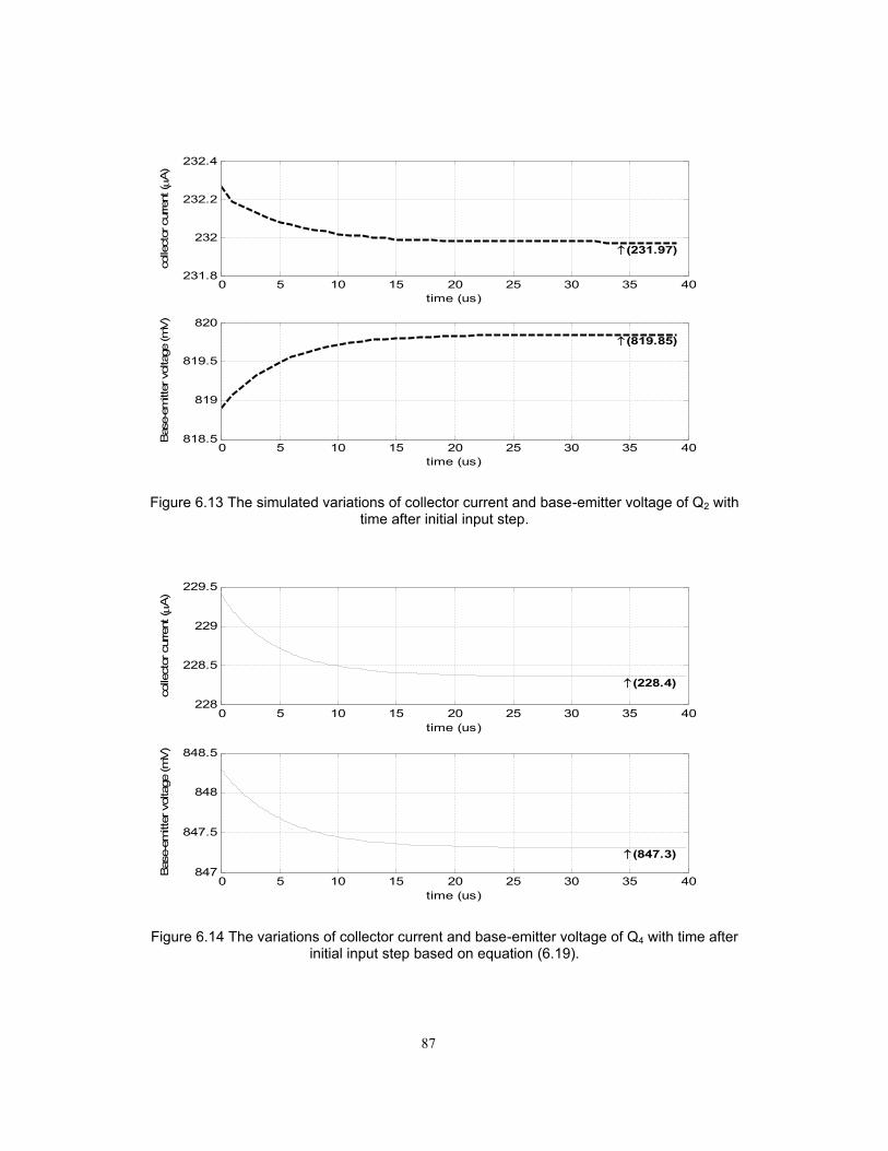
87
0 5 10 15 20 25 30 35 40231.8
232
232.2
232.4
time (us)
colle
ctor
cur
rent
( A)
(231.97)
0 5 10 15 20 25 30 35 40818.5
819
819.5
820
time (us)
Bas
e-em
itter
vol
tage
(mV)
(819.85)
Figure 6.13 The simulated variations of collector current and base-emitter voltage of Q2 with time after initial input step.
0 5 10 15 20 25 30 35 40228
228.5
229
229.5
time (us)
colle
ctor
cur
rent
( A)
(228.4)
0 5 10 15 20 25 30 35 40847
847.5
848
848.5
time (us)
Bas
e-em
itter
vol
tage
(mV)
(847.3)
Figure 6.14 The variations of collector current and base-emitter voltage of Q4 with time after initial input step based on equation (6.19).

88
0 5 10 15 20 25 30 35 40229
229.2
229.4
229.6
time (us)
colle
ctor
cur
rent
( A
)
(229.11)
0 5 10 15 20 25 30 35 40847
847.5
848
848.5
time (us)
Bas
e-em
itter
vol
tage
(mV
)
(847.35)
Figure 6.15 The simulated variations of collector current and base-emitter voltage of Q4 with time after initial input step.
6.4.2 Voltage Buffer Biased with a Current Mirror
Figure 6.16 shows a simple voltage buffer biased with a current mirror. If the input
voltage switches from low to high, the collector current of transistor Q5 decreases because of
the decrease of device operating temperature while the collector current of Q7 increases. The
thermal tail of bias currents are reflected to the base-emitter voltage change of transistors Q1
and Q3, and then reflected to the thermal tail of the output voltage. The mechanism of transient
operation in the current mirror is first investigated.
Below this branch notations are defined for simplicity: )0,0( thCC RtII ,
)finite,0(0, thCC RtII , )finite,0(0, thCC RtII ,
)finite,final(, thCfC RtII , and so on.

89
Since the topology in figure 6.16 is symmetrical, only the lower half of the transient
operation is examined here. The upper half is similar. Since the base-emitter voltage change of
Q6 and Q8 due to the static self-heating effect are much less than the supply voltage,
i.e. EECCBERthBERthVVVV 68 , the collector current of Q8 is assumed to be constant.
Hence the base-emitter voltage of Q8 decreases to cancel the increase in the collector current
of Q8 resulting from device temperature increase, i.e.
8,
888,
8,
88,
8Qm
thQQBEQQct
Qm
QRthQct
BEQRth gRIVg
g
TgV
. (6.20)
Therefore the collector currents of Q7 at different times are
87,777,0,7 BEQRthQmthQQCEQQctQCQ VgRIVgII , (6.21)
AinCQCQ VVII 10,70,7 , (6.22)
70,77,0,7,7 thQCQinQctCQfCQ RIVgII . (6.23)
Figure 6.16 Voltage buffer biased with current mirror.

90
The thermal tail of the collector current of Q7 is then reflected to the base-emitter
voltage of Q3. The collector current of Q3 at t=0- is
1)(
3
3
4
0,40,70,3
CQ
CQCQ
III , (6.24)
where
0,70,54
4,2,
22,44,
,4
444
,44,44,40,4
CQCQCQ
QmQm
QRthQctQRthQct
CEBQRth
thQCQEEQRth
CEBQRthQmQRthQctCQCQ
III
gg
TgTgV
RIVT
VgTgII
(6.25)
The collector currents of Q2 and Q4 have different variations because of the Early effect.
Thus similar to the procedure in section 6.4.1, the base-emitter voltage correction of Q2 and Q4
occurs to satisfy the KVL around the translinear loop and the KCL at node Vo. The base-emitter
voltage of Q4 at t=0+ tends to decrease from t=0- and the base-emitter voltage of Q3 will
increase. The collector current of Q4 at t=0+ is
CEBQEQmAQinCQCQ VgVVII ,44,40,40,4 1 , (6.26)
where
1)(
3
3
4
0,40,70,3
3,
0,30,33
4,2,
312,20,240,4
,4
CQ
CQCQ
Qm
CQCQBEQE
QmQm
EBQVinBEQVinQmAQinCQAQinCQ
CEBQE
III
gII
V
gg
VVgVVIVVIV
. (6.27)
Similarly the collector currents of Q2 and Q4 have different variations because of the
change of power dissipation after the initial input step. Following the procedure mentioned
before, the collector current of Q4 at t=final is
CEBQVinQmthQCQinQctCQfCQ VgRIVgII ,44,40,44,0,4,4 , (6.28)

91
4,2,
312,
4,2,
20,22,40,44,,4
QmQm
EBQVinBEQVinQm
QmQm
thQCQinQctthQCQinQctCEBQVin
gg
VVggg
RIVgRIVgV
, (6.29)
where
1)(
3
3
4
0,4,7,3
3,
0,3,33
CQ
fCQfCQ
Qm
CQfCQBEQVin
III
gII
V. (6.30)
Table 6.1 shows the collector currents and base-emitter voltages of transistors Q1
through Q8 at different time based on previous analysis, and table 6.2 shows the corresponding
simulation results. The input switch from 0 V to 1 V, time period is 4 ms, and the rise time is 1
ns. The thermal resistance of Q1 through Q8 is 3000 K/W, and the thermal capacitance is 1.69
nF as shown in the VBIC model attached in Appendix A. The thermal tail of Vo is
210,, BEVinBEVinofoV VVVVTTo
. (6.31)
The theoretical value of oV
TT is -2107 μV comparable to -2009 μV of the simulated value.
Table 6.1 Theoretical VBE and IC of Q1 through Q8 at different time

92
Table 6.2 Simulated VBE and IC of Q1 through Q8 at different time
6.5 Summary
The change of device temperature is an exponentially increasing function of time with a
time constant, τth=RthCth, and an asymptotic value of PthRth. The change of the base-emitter
voltage is also a function of time as VBE generally decreases with device temperature linearly.
The transient collector current of a BJT device can be estimated by considering the first order
dependence of collector current on the change of device temperature, the collector-emitter
voltage and the base-emitter voltage. The effect of self-heating on transient operation in the
high speed voltage buffer is analyzed and compared to the simulation results.

93
CHAPTER 7
DESIGN OF A SELF-HEATING TOLERANT CURRENT FEEDBACK
OPERATIONAL AMPLIFIER
This chapter examines the contribution of each transistor in a operational amplifier to
the overall thermal tail of current feedback amplifiers. A cascode bootstrapped CFOA is
proposed that minimizes the self-heating effect. The SPECTRE simulator verifies the design.
7.1 Superposition of the Overall Thermal Tail in CFOA
To design current feedback amplifiers free of a thermal tail, it is worthwhile to first look
at each transistor’s contribution in the total thermal tail. The overall thermal tail of a CFOA is a
linear addition of thermal tails caused by each transistor. Figure 7.1 shows the complete circuit
of the classical CFOA in figure 3.1 with emitter degeneration [24]. The complete circuit is
divided into six “sticks” from left to right as shown in figure 7.1. Every stick consists of vertically
connected transistors. According to the type and functionality of the transistors, each transistor
in a stick is named using the format, stkn-npn/pnp-bf or stkn-npn/pnp-cm for buffers or current
mirrors respectively. For example, Q8 belongs to stick3, and it is a part of the input buffer, so it
is called stk3-pnp-bf. While Q4 belongs to stick 2 and is a part of the current mirror, so it is
called stk2-pnp-cm. By enabling the self-heating effect in the transistor of interest and disabling
self-heating for the rest of the transistors, the contribution of each transistor to the total thermal
tail can be obtained [41]. Figure 7.2 shows the overall large-signal transient response of the
CFOA in figure 7.1 with input driven by a 2 V peak to peak square wave, in unity-gain non-
inverting configuration with a feedback resistor of 800 Ω. Table 7.1 shows the thermal tail
obtained at the output terminal, VO, of the CFOA in figure 7.1 caused by self-heating of each
individual transistor.
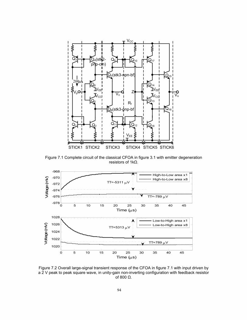
94
EE
CC
1 2
3 4
11 12
9 10 17
18
14
13
15
16
on
EE
CC
6
5
7
8
p
f
EE
CC
Figure 7.1 Complete circuit of the classical CFOA in figure 3.1 with emitter degeneration resistors of 1kΩ.
0 5 10 15 20 25 30 35 40 45-978
-976
-974
-972
-970
-968
Time (s)
Vol
tage
(mV)
0 5 10 15 20 25 30 35 40 45
1020
1022
1024
1026
1028
Time (s)
Vol
tage
(mV)
High-to-Low area x1High-to-Low area x8
Low-to-High area x1Low-to-High area x8
TT=-5311 V
TT=5313 V
TT=789 V
TT=-789 V
Figure 7.2 Overall large-signal transient response of the CFOA in figure 7.1 with input driven by a 2 V peak to peak square wave, in unity-gain non-inverting configuration with feedback resistor
of 800 Ω.

95
Table 7.1 Thermal tail obtained at terminal VO of the CFOA in figure 7.1 caused by self-heating of each individual transistor, in unity-gain non-inverting configuration with feedback
resistor of 800 Ω [41]
Area 1x5 μm2 Area 8x5 μm2
Thermal Tail (uV/V) High-to-Low Low-to-High High-to-Low Low-to-High
stk2-npn-bf (Q5) 822 -842 124 -128 stk2-pnp-bf (Q6) 727 -712 101 -98 stk2-npn-cm (Q2) 89 -91 11 -12 stk2-pnp-cm (Q4) 91 -89 10 -9 stk3-npn-bf (Q7) 877 -850 111 -106 stk3-pnp-bf (Q8) 783 -808 111 -115
stk4-npn-cm (Q12) 1213 -1217 172 -173 stk4-pnp-cm (Q10) 1075 -1073 159 -158 stk5-npn-bf(Q13) -13 13 -2 2 stk5-pnp-bf(Q14) 4 -4 1 -1 stk5-npn-cm(Q18) -16 15 -2 2 stk5-pnp-cm(Q17) 5 -2 0 0 stk6-npn-bf(Q15) 0 -1 0 0 stk6-pnp-bf(Q16) 1 0 0 0
Sum of the thermal tails above 5658 -5661 796 -796 Overall simulated thermal tail 5311 -5313 789 -789
As shown in Table 7.1, the overall thermal tail mainly comes from the input power
transistors, Q5 (stk2-npn-bf), Q6 (stk2-pnp-bf), Q7 (stk3-npn-bf) and Q8 (stk3-pnp-bf), and from
the current mirrors of the trans-impedance stage, Q10 (stk4-pnp-cm) and Q12 (stk4-npn-cm). The
overall thermal tail is a linear addition of the thermal tails contributed by each transistor of the
CFOA. Note that the current mirror transistors to bias the output stage, Q17 (stk5-npn-cm) and
Q18 (stk5-pnp-cm), contribute negligible amount to the overall thermal tail because of the double
voltage buffer configuration at the output stage. Also the power transistors in the output stage,
Q13 (stk5-npn-bf) and Q16 (stk5-pnp-bf), Q15 (stk6-npn-bf) and Q16 (stk6-pnp-bf) contribute
negligible thermal tail to the overall thermal tail because of the large magnitude of
transimpedance and negative feedback. This can be verified by the following analysis.
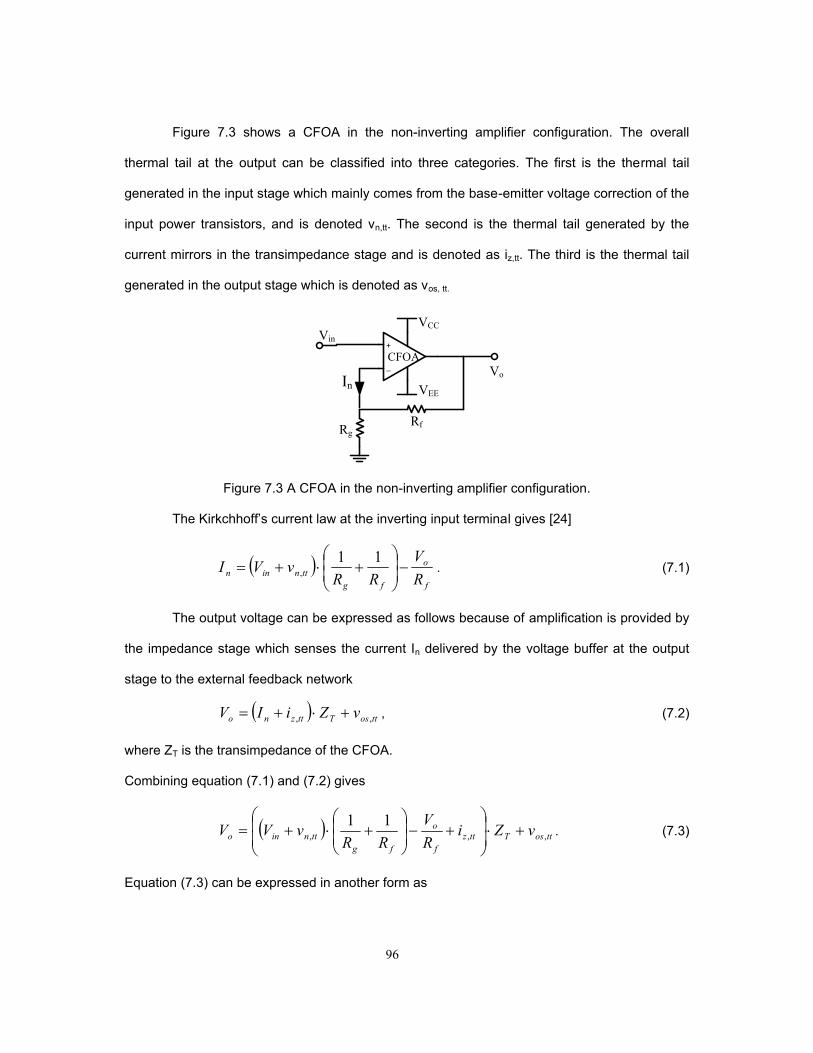
96
Figure 7.3 shows a CFOA in the non-inverting amplifier configuration. The overall
thermal tail at the output can be classified into three categories. The first is the thermal tail
generated in the input stage which mainly comes from the base-emitter voltage correction of the
input power transistors, and is denoted vn,tt. The second is the thermal tail generated by the
current mirrors in the transimpedance stage and is denoted as iz,tt. The third is the thermal tail
generated in the output stage which is denoted as vos, tt.
+
–
fg
o
inCC
EEn
CFOA
Figure 7.3 A CFOA in the non-inverting amplifier configuration.
The Kirkchhoff’s current law at the inverting input terminal gives [24]
f
o
fgttninn R
VRR
vVI
11, . (7.1)
The output voltage can be expressed as follows because of amplification is provided by
the impedance stage which senses the current In delivered by the voltage buffer at the output
stage to the external feedback network
ttosTttzno vZiIV ,, , (7.2)
where ZT is the transimpedance of the CFOA.
Combining equation (7.1) and (7.2) gives
ttosTttzf
o
fgttnino vZi
RV
RRvVV ,,,
11
. (7.3)
Equation (7.3) can be expressed in another form as

97
ttosTttzf
T
g
fttnin
f
To vZi
RZ
RR
vVRZV ,,, 11
(7.4)
Assuming Rg=∞ in unity gain configuration and ZT>>Rf and, equation (7.4) becomes
fT
ttosfttzttnino RZ
vRivVV
1,
,, , (7.5)
where fT
ttos
RZv
1, is negligible. This explains why the thermal tail contributed from the power
transistors in the output stage is negligible.
7.2 Cascode Bootstrapped CFOA
Table 7.1 shows that the overall thermal tail is reduced about 8 times when the size of
each transistor in the CFOA of figure 7.1 is increased 8 times. The thermal resistance
decreases with increasing area of a transistor. But this is not an attractive technique because of
the large area requirement. As discussed in chapter 5, techniques that raise the effective output
resistance can reduce effects of self-heating. These techniques include cascoding, negative
feedback as with the Wilson current mirror, or emitter degeneration.
Figure 7.4 shows four possible cascode half-circuits of the input stage that can raise the
effective output resistance [40]. Here a single buffer is used rather than a double buffer because
of the double buffer’s offset voltage. In the circuit shown in figure 7.4.(a), the base of Q3 is
bootstrapped to the inverting input, Vn, by two diode connected transistors. This is called
reverse bootstrapping [40]. The effective output resistance at the collector of Q3 is
approximately equal to βro. In the circuit shown in figure 7.4.(b), a beta helper, Q8, is used to
increase the slew rate by making more current available at the base of Q2. In figure 7.4.(c) the
base of Q3 is bootstrapped to the non-inverting input, Vp, rather than the inverting input by two
diode connected transistors. This is called forward bootstrapping [40]. The circuit in figure 7.4.(d)
improves offset voltage by keeping the collector-base voltage of Q1 and Q2 same (≈0).
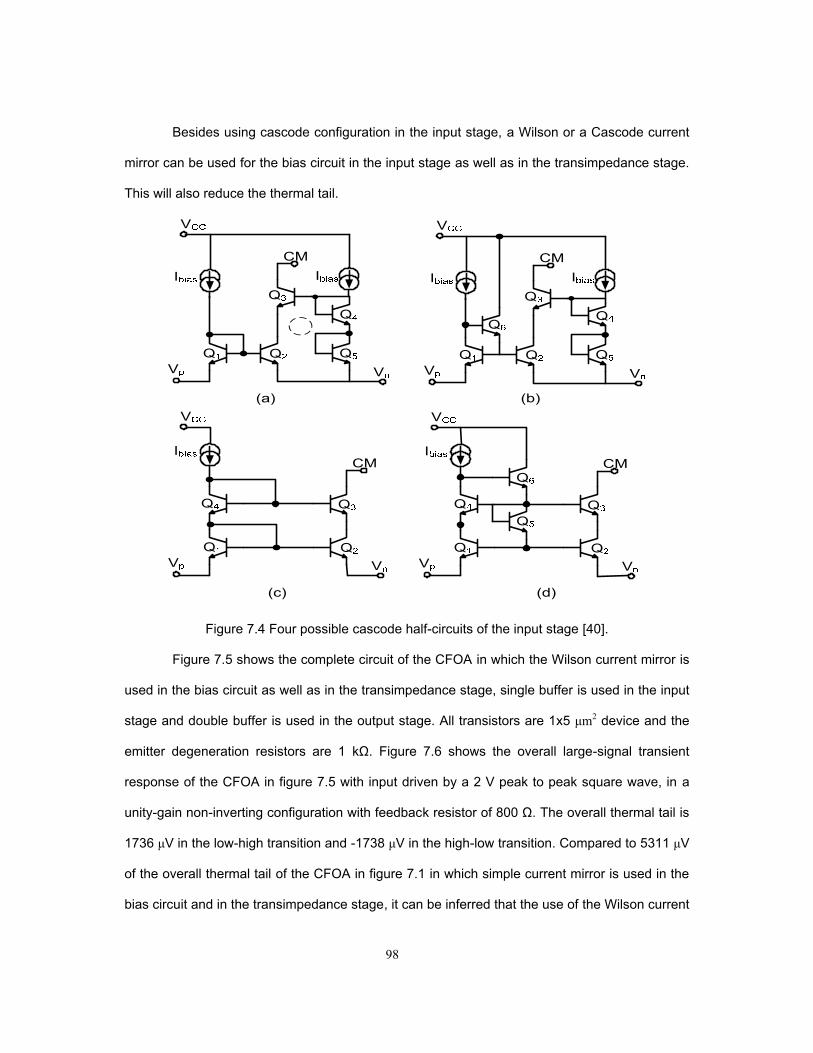
98
Besides using cascode configuration in the input stage, a Wilson or a Cascode current
mirror can be used for the bias circuit in the input stage as well as in the transimpedance stage.
This will also reduce the thermal tail.
Figure 7.4 Four possible cascode half-circuits of the input stage [40].
Figure 7.5 shows the complete circuit of the CFOA in which the Wilson current mirror is
used in the bias circuit as well as in the transimpedance stage, single buffer is used in the input
stage and double buffer is used in the output stage. All transistors are 1x5 μm2 device and the
emitter degeneration resistors are 1 kΩ. Figure 7.6 shows the overall large-signal transient
response of the CFOA in figure 7.5 with input driven by a 2 V peak to peak square wave, in a
unity-gain non-inverting configuration with feedback resistor of 800 Ω. The overall thermal tail is
1736 μV in the low-high transition and -1738 μV in the high-low transition. Compared to 5311 μV
of the overall thermal tail of the CFOA in figure 7.1 in which simple current mirror is used in the
bias circuit and in the transimpedance stage, it can be inferred that the use of the Wilson current

99
mirror in the bias circuit as well as in the transimpedance stage greatly suppress the self-
heating effects.
Figure 7.5 Complete circuit of the CFOA with Wilson current mirror at the input and transimpedance stage. All transistors are 1x5 μm2 device. Emitter degeneration resistors are
1kΩ.
0 5 10 15 20 25 30 35 40 45-992
-991
-990
-989
-988
-987
Time (s)
Voltage
(mV)
0 5 10 15 20 25 30 35 40 451007
1008
1009
1010
Time (s)
Voltage
(mV)
Low-to-High without self-heatingLow-to-High with self-heating
High-to-Low without self-heatingHigh-to-Low with self-heating
TT=-1738 V
TT=1736 V
Figure 7.6 Overall large-signal transient response of the CFOA in figure 7.5 with input driven by a 2 V peak to peak square wave, in unity-gain non-inverting configuration with feedback resistor
of 800 Ω.

100
Figure 7.7 shows the complete cascode reverse bootstrapped CFOA [40]. Transistors
Q23 and Q24 are cascode devices to improve the output resistance of Q9 and Q10, respectively;
Q26 and Q27 are used to bootstrap the base of Q23 to the inverting input; Q28 and Q29 are used to
bootstrap the base of Q24 to the inverting input. Wilson current mirrors are used in the biasing
circuit of the input stage and the transimpedance stage. Single voltage buffer is used at both the
input stage and the output stage. Q25 and Q30 are used to bias Q26 through Q29. With the
technique of cascoding, the power transistors in the input stage, Q9 and Q10, hardly contribute
any to the overall thermal tail as shown in Table 7.2.
Figure 7.7 Complete circuit of the cascode reverse bootstrapped CFOA. Q23 and Q24 are cascode devices to improve the output resistance of Q9 and Q10, respectively [40].

101
It can be inferred that the thermal tail, introduced by Q25 and Q30 is opposite to that
introduced by Q18 (stk5-pnp-cm) and Q17 (stk5-npn-cm) in figure 7.7. Therefore, the overall
thermal tail can be minimized by making the thermal tail caused by Q25 and Q30 to be equal and
opposite to the thermal tail caused by stk5-cm (Q17 and Q18). This can be done by optimizing
the areas of transistors in a specific stick selectively. It is found that by setting the areas of
transistor from stick1 to stick 4 to 8x5 μm2, and from stick5 and stick6 to 64x5 μm2, the overall
thermal tail is minimized to around 19 μV as shown in figure 7.8 and Table 7.2 for the CFOA in
figure 7.7.
0 5 10 15 20 25 30 35 40 45-993
-992
-991
-990
-989
Time (s)
Vol
tage
(mV
) High-to-Low without self-heatingHigh-to-Low with self-heating
0 5 10 15 20 25 30 35 40 451007
1008
1009
1010
1011
Time (s)
Vol
tage
(mV
)
Low-to-High without self-heatingLow-to-High with self-heating
Figure 7.8 Overall large-signal transient response of the cascode reverse bootstrapped CFOA in figure 7.7 with input driven by a 2 V peak to peak square wave, in unity-gain non-inverting
configuration with feedback resistor of 800 Ω.

102
Table 7.2 Thermal tail obtained at terminal VO of the CFOA in figure 7.5 and 7.7 caused by self-heating of each individual transistor, in unity-gain non-inverting configuration with feedback
resistor of 800 Ω [41]
Figure 7.9 shows the overall thermal tails when the classic CFOA in figure 7.5 and the
cascode bootstrapped CFOA in figure 7.7 drive a load of 2 kΩ and 2 pF. The input is a 1 V peak
to peak square wave. The area of the transistors Q19 and Q20, Q21 and Q22 is set to 64x5 μm2,
2048x5 μm2, respectively in order to drive the load of 2 kΩ and 2 pF. The overall thermal tail of
the classic CFOA in figure 7.5 is 1032 μV while the overall thermal tail of the cascode
bootstrapped CFOA in figure 7.7 is 9 μV. For all loads, a similar reduction should be expected.

103
0 5 10 15 20 25 30 35 40507
507.5
508
508.5
time (us)
Out
put V
olta
ge (m
V)
RL=2 k ,CL=2 pF,the classic CFOA in fig.7.5
0 5 10 15 20 25 30 35 40506.52
506.525
506.53
506.535
time (us)
Out
put V
olta
ge (m
V) RL=2 k ,CL=2 pF,cascode bootstrapped CFOA in fig.7.7
1032 V
9 V
Figure 7.9 The overall thermal tails of the classic CFOA in figure 7.5 and the cascode bootstrapped CFOA in figure 7.7 when driving a load of 2 kΩ and 2 pF
7.3 Other CFOA Parameters
For all the simulation in this section, the SPECTRE simulator is used. The model used
is attached in Appendix A. The power supply voltages are set to VCC=+5V, and VEE=-5 V.
Figure 7.10 shows the inverting input DC current transfer curve of the cascode reverse
bootstrapped CFOA in figure 7.7. As shown in figure 7.10, the DC input offset current, Ioffset, is
equal to -5.898 μA. By applying Ioffset to the inverting input terminal, the transimpedance
frequency response is obtained as in figure 7.11. The low frequency transimpedance is around
1.8 MOhms. Since a Wilson current mirror is used in the transimpedance stage, the effect of
self-heating is minimized at low frequencies.

104
Figures 7.12 and 7.13 show the positive and negative power rejection ratio of the
cascode reverse bootstrapped CFOA in figure 7.7. The positive PSRR is about 63.26 dB and
the negative PSRR is about 60.1 dB.
Figure 7.14 shows the DC voltage transfer curve of the cascode reverse bootstrapped
CFOA in figure 7.7. The input offset voltage is about -0.652 mV. By applying the input offset
voltage at the input, the common mode rejection ratio frequency response is obtained in figure
7.15. The CMRR is around 95.6 dB. Due to the use of cascode topology in the input stage, the
CMRR is greatly improved.
Figure 7.16 shows the simulation result of the common mode input range via the
configuration in figure 3.11. Resistors of 2 kΩ are used here. As shown in figure 7.16, the
positive CMIR is 2.96 V, and the negative CMIR is -2.98 V.
-12 -10 -8 -6 -4 -2 0-4
-3
-2
-1
0
1
2
3
4
Input Offset Current (A)
Out
put V
olta
ge (V
)
Figure 7.10 DC Current transfer curve of the cascode reverse bootstrapped CFOA in figure 7.7.

105
100 102 104 106 1080
0.2
0.4
0.6
0.8
1
1.2
1.4
1.6
1.8
2
Frequency (Hz)
Mag
nitu
de o
f Tra
nsim
pede
nce
(MO
hms)
Figure 7.11 Transimpedance of the cascode reverse bootstrapped CFOA in figure 7.7.
100 102 104 106 1080
10
20
30
40
50
60
70
Frequency (Hz)
PSRR+
(dB)
Figure 7.12 Positive PSRR of the cascode reverse bootstrapped CFOA in figure 7.7.

106
100 102 104 106 1080
10
20
30
40
50
60
70
Frequency (Hz)
PSRR- (
dB)
Figure 7.13 Negative PSRR of the cascode reverse bootstrapped CFOA in figure 7.7
-10 -8 -6 -4 -2 0 2 4 6 8 10-4
-3
-2
-1
0
1
2
3
4
Input Offset Voltage (mV)
Out
put V
olta
ge (V
)
Figure 7.14 DC voltage transfer curve of the cascode reverse bootstrapped CFOA in figure 7.7

107
100 102 104 106 1080
10
20
30
40
50
60
70
80
90
100
Frequency (Hz)
CM
RR (d
B)
Figure 7.15 CMRR of the cascode reverse bootstrapped CFOA in figure 7.7
-8 -6 -4 -2 0 2 4 6 8-0.5
-0.4
-0.3
-0.2
-0.1
0
0.1
0.2
0.3
0.4
0.5
Input Voltage (V)
Out
put V
olta
ge (V
)
Figure 7.16 CMIR of the cascode reverse bootstrapped CFOA in figure 7.7

108
7.4 Summary
An approach to analyze the contribution of each transistor to the overall thermal tail of a
current feedback operational amplifier is presented. It is shown that the overall thermal tail of a
CFOA is a linear superposition of each individual transistor. Techniques to minimize the thermal
tail are proposed. A cascode bootstrapped CFOA is designed and optimized to minimize the
thermal tail. The overall thermal tail is reduced to 9 μV/V compared with 1032 μV/V of a
classical CFOA when driving a 2 kΩ load in unity gain feedback configuration. For all loads, a
similar reduction of the thermal tail should be expected. Also the common mode rejection ratio
(CMRR) is greatly improved to 92 dB compared with 60 dB of the classical CFOA. Note that the
common mode input range (CMIR) is sacrificed in order to get reduced thermal tail.

109
CHAPTER 8
CONCLUSIONS AND FUTURE WORK
Self-heating effects have been studied extensively in large-signal behavior, small-signal
behavior and transient behavior for silicon-on-insulator (SOI) bipolar junction transistors. For a
bipolar junction transistor (BJT) driven by a constant base-emitter voltage, self-heating can
significantly increase the collector current. If the base is driven by a constant current source,
self-heating increases collector current very slowly. By knowing the thermal resistance, the
power dissipated and the mobility exponent factor, DC errors caused by self-heating effects can
be roughly estimated. A simple method of extracting the thermal resistance and the Early
voltage is proposed avoiding precise junction temperature control. It is shown that self-heating
effects can strongly affect the output impedance of a BJT, and hence the gain of an amplifier by
inducing a thermal zero-pole pair at lower frequencies than the intrinsic pole. Techniques raising
the effective output impedance can reduce such error due to self-heating. These techniques
include cascoding and negative feedback as done with Wilson current mirrors or emitter
degeneration. In the transient operation, the change of device operating temperature is an
exponentially increasing function of time with a time constant of the product of the thermal
resistance and the thermal capacitance. Therefore, the settling time of switching circuits can be
significantly degraded by self-heating since thermal transients take a much longer time to settle.
Also the change of device operating temperature due to the change of power dissipation can
cause the base-emitter voltage correction, current correction and consequently the thermal tail
in the output. By knowing the thermal resistance, the power dissipated and the typical
temperature coefficient, an approach to estimate thermal tails is presented. The thermal tail of a
high speed voltage buffer biased with a current mirror is analyzed via this approach.

110
An analysis of the contribution of each transistor in a current feedback operational
amplifier to the overall thermal tail is presented. It is shown that the overall thermal tail of a
current feedback operational amplifier is a linear superposition of each individual transistor. By
balancing the positive and negative thermal tail together via a cascode bootstrapped circuit
topology, and using a Wilson current mirror in the biasing stage and transimpedance stage, the
overall thermal tail is reduced to 9 μV/V compared with 1032 μV/V of a classical CFOA when
driving a 2kΩ load in a unity gain feedback configuration. For all loads, a similar reduction of the
thermal tail should be expected. Also the common mode rejection ratio (CMRR) is greatly
improved from 60 dB of the classical CFOA to 92 dB.
The design of a low-voltage, rail to rail BJT current feedback operational amplifier would
be an interesting topic. Self-heating effects on distortion of bipolar junction transistor would be
another topic to look into. Also the analysis of self-heating effects on voltage feedback
operational amplifier would be worthwhile.

111
APPENDIX A
BIPOLAR JUCNTION TRANSISTOR MODEL FILE [10]

112
A summary of the VBIC and SGP model parameters in SPECTRE format for the NPN
and PNP transistors is provided in this appendix. These parameters are not meant to
characterize any true proprietary specific SOI process technology. The emitter area of the NPN
and PNP transistors listed in this appendix is 1x5 μm2.
.model qinn vbic type=NPN +IS=5.45E-18 NF=1.0 NR=1.0 RBX=30.0 RCX=10.0 +RCI=100.0 VO=5.0 GAMM=1.0E-10 HRCF=1.1E03 QCO=1.0E-15 +RBI=3.70E02 RE=15.0 RS=1.0E07 FC=9.0E-01 CJC=1.0E-14 +CJEP=2.1E-15 PC=0.73 MC=2.50E-01 AJC=-0.5 CJCP=5.0E-15 +CJE=4.70E-15 PE=0.93 ME=3.33E-01 AJE=-0.5 AJS=-0.5 +IBEI=4.66E-20 NEI=1.0 IBEN=7.50E-15 NEN=2.0 IBCI=2.02E-18 +NCI=1.0 NCN=2.0 IBCN=5.97E-16 AVC1=2.0 AVC2=50.0 +NCNP=2.0 VEF=78.0 VER=2.5 IKP=2.0E-04 IKF=2.73E-03 +IKR=1.52E-02 XTF=10.0 TF=4.42E-12 QTF=0.3 VTF=2.5 +ITF=3.04E-03 AFN=2.0 TR=1.77E-09 TD=7.72E-12 KFN=1.0E-09 +BFN=1.0 EA=1.13 EAIE=1.12 EAIC=1.12 EAIS=1.12 +EANE=1.12 EANC=1.12 EANS=1.12 XIS=3.50 XII=1.70 +XIN=1.7 TNF=0.0 IMELT=1.0E3 RBP=1.0 CBEO=1.01E-16 +CBCO=2.02E-16 XVO=0 PS=1.0 MS=0 WBE=1 +ISP=0.0 WSP=1.0 NFP=1.0 IBEIP=0.0 IBENP=0 +IBCIP=0 NCIP=1 IBCNP=0 XRE=0 XRB=0 +XRC=0 XRS=0 TAVC=0 SELFT=1 +CTH=1.67E-09 RTH=3000.0 TNOM=25.0 .model qinp vbic type=PNP +IS=2.42E-18 NF=1.0 NR=1.0 RBX=13.33 RCX=22.50 +RCI=225.0 VO=2.22 GAMM=4.44E-11 HRCF=1.0E03 QCO=2.25E-15 +RBI=164.44 RE=33.75 RS=1.0E07 FC=9.0E-01 CJC=1.0E-14 +CJEP=2.1E-15 PC=0.73 MC=2.50E-01 AJC=-0.5 CJCP=5.0E-15 +CJE=4.70E-15 PE=0.93 ME=3.3E-01 AJE=-0.5 AJS=-0.5 +IBEI=3.76E-20 NEI=1.0 IBEN=7.50E-15 NEN=2.0 IBCI=8.97E-19 +NCI=1.0 NCN=2.0 IBCN=5.97E-16 AVC1=3.0 AVC2=55.0 +NCNP=2.0 VEF=26.0 VER=1.5 IKP=2.0E-04 IKF=1.2E-03 +IKR=6.75E-03 XTF=22.50 TF=4.98E-12 QTF=0.3 VTF=2.5 +ITF=1.35E-03 AFN=2.0 TR=1.99E-09 TD=8.68E-12 KFN=6.26E-10 +BFN=1.0 EA=1.13 EAIE=1.12 EAIC=1.12 EAIS=1.12 +EANE=1.12 EANC=1.12 EANS=1.12 XIS=3.15 XII=0.76 +XIN=0.76 TNF=0.0 IMELT=1.0E3 RBP=1.0 CBEO=1.01E-16 +CBCO=2.02E-16 XVO=0 PS=1.0 MS=0 WBE=1 +ISP=0.0 WSP=1.0 NFP=1.0 IBEIP=0.0 IBENP=0 +IBCIP=0 NCIP=1 IBCNP=0 XRE=0 XRB=0 +XRC=0 XRS=0 TAVC=0 SELFT=1 +CTH=1.67E-09 RTH=3000.0 TNOM=25.0

113
.model npn NPN struct=vertical +IS=6.06E-18 BF=130.00 NF=1.00 +VAF=156.00 IKF=3.04E-03 ISE=1.26E-15 +NE=2.00 BR=3.00 NR=1.00 +VAR=5.00 IKR=3.04E-02 ISC=6.06E-17 +NC=1.00 RB=400.00 RBM=30.00 +IRB=1.00E-03 RE=15.00 RC=10.00 +CJC=1.03E-14 VJC=7.32E-01 MJC=2.50E-01 +CJE=4.70E-15 VJE=9.28E-01 MJE=3.33E-01 +XCJC=1.00E+00 CJS=5.00E-15 VJS=6.55E-01 +MJS=0.00E+00 TR=1.77E-09 KF=1.00E-09 +AF=2.00 EG=1.13 XTB=0.00E+00 +XTI=4.00 FC=0.50 TF=1.77E-11 +XTF=10.00 VTF=2.50 ITF=1.00E-03 +PTF=25.00 TNOM=25.00 .model pnp PNP struct=vertical +IS=2.69E-18 BF=71.50 NF=1.00 +VAF=52.00 IKF=1.35E-03 ISE=1.26E-15 +NE=2.50 BR=4.00 NR=1.00 +VAR=3.00 IKR=1.35E-02 ISC=2.69E-17 +NC=1.00 RB=177.78 RBM=13.33 +IRB=4.44E-04 RE=33.75 RC=22.50 +CJC=1.03E-14 VJC=7.32E-01 MJC=2.50E-01 +CJE=4.70E-15 VJE=9.28E-01 MJE=3.33E-01 +XCJC=1.00E+00 CJS=5.00E-15 VJS=6.55E-01 +MJS=0.00E+00 TR=1.99E-09 KF=3.43E-10 +AF=2.00 EG=1.13 XTB=0.00E+00 +XTI=4.00 FC=0.50 TF=1.99E-11 +XTF=100.00 VTF=2.50 ITF=1.35E-03 +PTF=30.00 TNOM=25.00

114
REFERENCES
[1] P.R. Ganci, J.-J.J. Hajjar, T. Clark, P. Humphries, J. Lapham, and D. Buss, “Self-
Heating in High Performance Bipolar Transistors Fabricated on SOI Substrates,”
Technical Digest International, Electron Devices Meeting, pp. 417-420, Dec. 1992.
[2] Michael Maida, “National Semiconductor Develops Complementary Bipolar Process for
High Speed, High performance Analog”, 2001.
[3] Fujiang Lin, Tianshu Zhou, Bo Chen, Ban Leong Ooi and Pang Shyan Kooi, “Extraction of
VBIC Model for Si-Ge HBTs Made Easy by going through. Gummel-Poon Model”,
Singapore Microelectronics Modeling Center (SMMC), Nov. 2000.
[4] X. Cao, J. McMacken, K. Stiles, P. Layman, J.J. Liou, A. Sun, and S. Moinian, "Parameter
extraction and optimization for new industry standard VBIC model," Advanced
Semiconductor Devices and Microsystems, Second International Conf., pp.107-116, Oct.
1998
[5] C. McAndrew, J. Seitchik, D. Bowers, M. Dunn, M. Foisy, I. Getreu, M. McSwain, S.
Moinian, J. Parker, P. van Wijnen, and L. Wagner, "VBIC95: An improved vertical, IC
bipolar transistor model," Bipolar/BiCMOS Circuits and Technology Meeting, pp. 170-177,
Oct. 1995.
[6] Kull, G. M., Nagel, L. W., Lee, S.-W., Lloyd, P., Prendergast, E. J., and Dirks, H. K., “A
unified circuit model for bipolar transistors including quasi-saturation effects”, IEEE Trans.
on Electron Device, Vol. 32, pp. 1103-1113, 1985.
[7] Stubing, H. and Rein, H.-M., “A compact physical large-signal model for high-speed bipolar
transistors at high current densities-Part I: one-dimensional model”, IEEE Trans. on
Electron Device, 34, pp. 1741-1751, 1987.
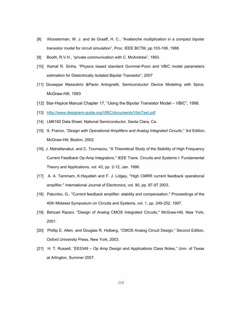
115
[8] Kloosterman, W. J. and de Graaff, H. C., “Avalanche multiplication in a compact bipolar
transistor model for circuit simulation”, Proc. IEEE BCTM, pp.103-106, 1988.
[9] Booth, R.V.H., “private communication with C. McAndrew”, 1993.
[10] Kamal R. Sinha, “Physics based standard Gummel-Poon and VBIC model parameters
estimation for Dielectrically Isolated Bipolar Transistor”, 2007
[11] Giuseppe Massobrio &Paolo Antognetti, Semiconductor Device Modeling with Spice,
McGraw-Hill, 1993
[12] Star-Hspice Manual Chapter 17, “Using the Bipolar Transistor Model – VBIC”, 1998.
[13] Http://www.designers-guide.org/VBIC/documents/VbicText.pdf
[14] LM6182 Data Sheet, National Semiconductor, Santa Clara, Ca.
[15] S. Franco, “Design with Operational Amplifiers and Analog Integrated Circuits,” 3rd Edition,
McGraw-Hill, Boston, 2002.
[16] J. Mahattanakul, and C. Toumazou, "A Theoretical Study of the Stability of High Frequency
Current Feedback Op-Amp Integrators," IEEE Trans. Circuits and Systems I: Fundamental
Theory and Applications, vol. 43, pp. 2-12, Jan. 1996.
[17] A. A. Tammam, K.Hayatleh and F. J. Lidgey, "High CMRR current feedback operational
amplifier," International Journal of Electronics, vol. 90, pp. 87-97 2003.
[18] Palumbo, G., "Current feedback amplifier: stability and compensation," Proceedings of the
40th Midwest Symposium on Circuits and Systems, vol. 1, pp. 249-252, 1997.
[19] Behzad Razavi, "Design of Analog CMOS Integrated Circuits," McGraw-Hill, New York,
2001.
[20] Phillip E. Allen, and Douglas R. Holberg, “CMOS Analog Circuit Design,” Second Edition,
Oxford University Press, New York, 2003.
[21] H. T. Russell, “EE5349 – Op Amp Design and Applications Class Notes,” Univ. of Texas
at Arlington, Summer 2007.
116
[22] Koullias, I.A., "A wideband low-offset current-feedback op amp design," Proceedings of
the 1989 Bipolar Circuits and Technology Meeting, pp. 120-123, 1989.
[23] S. O. Smith, “The good, the bad and the ugly: current feedback - technical contributions
and limitations,” IEEE Circuits and Systems, ISCAS ’93, 1993 IEEE International
Symposium, pp. 1058 – 1061, 1993.
[24] Alan Buchholz, “Current Feedback OpAmp Design”, Oct. 2006
[25] Franco, S., “Analytical foundations of current-feedback amplifiers,” Circuits and Systems,
ISCAS '93, 1993 IEEE International Symposium, pp. 1050 – 1053, 1993.
[26] R. M. Fox, S.- G Lee, and D.T. Zweidinger, “The Effects of BJT Self-Heating on Circuit
Behavior,” IEEE J. Solid-State Circuits, vol. 28, pp. 678-685, Jun. 1993.
[27] Sang-Gug Lee, “A Review of Self-Heating Effects on Bipolar Circuits,” in Proc.
Southcon/94. Conf, pp. 138-142, Oct. 1994.
[28] W. G. Oldsam and S.E. Schwarz, An Introduction to Electronics, Holt, Rinehart and
Winston, New York, 1972.
[29] N. Nenadovic & etc, “Analytical formulation and electrical measurements of self-heating in
silicon BJT’s”, IEEE BCTM 1.2, 2002.
[30] S.E. Swirhun, Y.H. Kwark and R.M. Swanson, “Measurement of electron lifetime, electron
mobility, and bandgap narrowing in heavily doped p-type silicon”, IEDM Technical Digest,
24, 1986.
[31] J. del. Alamo, S.E. Swirhun and R.M. Swanson, “Simultaneous measurement of hole
ifetime, hole mobility, and bandgap narrowing in heavily doped n-type silicon”, IEDM
Technical Digest, 290, 1985.
[32] Bart Van Zeghbroeck, Principles of Semiconductor Devices, Prentice Hall, 2008.
[33] Paul R. Gray, Paul J. Hurst, Stephen H. Lewis, and Robert G. Meyer, "Analysis and
Design of Analog Integrated Circuits," 4th Edition, Wiley, 2001

117
[34] Dale BuHanan, “Investigation of Current-Gain Temperature Dependence in Silicon
Transistors”, IEEE Transactions on Electron Devices, vol. ED-16, January, 1969.
[35] Yang-Hua Chang, Zhi-Juan Chang, Hui-Feng Hsu, "Extraction of Early Voltage and
Thermal Resistance in InP/InGaAs HBTs", IEEE Conference on Electron Devices and
Solid-State Circuits, 2005.
[36] Morten Olavsbraten, “A Practical Method of Parameter Extraction for the VBIC Model
used on a GaAs HBT”, in Gallium Arsenide applications symposium, 2000.
[37] Bhalla, A., Chow, T.P., Meng-Kai Chen, “Temperature dependence of gummel-poon
model parameters from -40 ≤ T ≤ 1850C for medium-voltage, junction-isolated BJT's”,
Proceedings of the 4th International Symposium on Power Semiconductor Devices and
ICs, 1992.
[38] Shaikh F. Shams, Colin C. McAndrew, Ik-Sung Lim, and Anna Zlotnicka, "SiGe HBT Self-
Heating Modeling and Characterization from AC data," in Proc. BCTM, pp. 92-95, Sept-
Oct. 2002.
[39] Kamal R. Sinha, Ronald L. Carter, Howard T. Russell, and W. Alan Davis, “Impact of Self-
Heating on Frequency Response of Current Mirrors in Bipolar Technology,” Region 5
Technical Conference, April 2008.
[40] A. A. Tammam, K. Hayatleh, B. Hart, and F. J. Lidgey, “A Hierarchy of Input Stages for
Current Feedback Operational Amplifiers,” International Symposium, Circuits and Systems,
vol. 1, pp. 821-824, May 2004.
[41] Kamal R. Sinha, Xuesong Xie, Ronald L. Carter, W. Alan Davis, and Howard T. Russell,
“Thermal Effects in Current Feedback Operational Amplifiers in Bipolar Technology,”
Region 5 Technical Conference, April 2008.

118
BIOGRAPHICAL INFORMATION
Xuesong Xie was born in Guizhou, China in 1975. He received his Bachelor of
Engineering degree in Electrical Engineering from Huazhong University of Science &
Technology, Wuhan, China in May 1997. He received his Master of Science degree in Electrical
Engineering from Huazhong University of Science & Technology, Wuhan, China in May 2000.
He began working towards his Ph.D. degree in Electrical Engineering from fall 2000 at the
University of Texas at Arlington. From January 2002, he began working in the Analog Integrated
Circuits Design Laboratory under the guidance of Dr. Ronald L. Carter and Dr. W. Alan Davis.
His research interest focuses on Current Feedback Amplifier design and functionality analysis.
He acquired his Ph.D. degree in May 2010.