The real time digital simulation of single phase vsc and...
5
International Conference on Power Systems Transients - IPST 2003 in New Orleans, USA The Real Time Digital Simulation of a Single Phase Voltage Source Converter and its Application Ming Yu 1 , Hiroo Konishi 2 (1) RTDS Technologies, Inc., 200-1619 Pembina Hwy, Winnipeg, Manitoba, Canada, R3T 3Y6 (e-mail: [email protected]), (2) Substation System Engineering Div., Power & Industrial System, Hitachi Ltd., 1-1-1 Kokubu-cho, Hitachi-shi, Ibaraki, Japan 316-8051 (email: [email protected]) Abstract – Voltage Source Converters (VSCs) use Gate Turn- Off (GTO) devices and Pulse Width Modulation (PWM) technology to control the operation of the converter bridge. This paper presents a new fully digital model of a single phase VSC. The unique improved firing algorithm (a numerical algorithm for compensating discrete time step firing error) allows the simulation time step to be in the range of 50 S while maintaining the high firing accuracy required by PWM. The real time network solution algorithm of the RTDS simulator makes it possible to inter-connect the VSC models with any other models in the RTDS power systems library. As a result, complex schemes of inter-connected single phase VSCs can be studied in real time. Physical controllers can also be tested using the model. Keywords –voltage source converter, real time digital simulator, power electronics, PWM I. INTRODUCTION The Voltage Source Converter is a building block of FACTS devices such as STATCOM and UPFC. Single phase voltage source converters can be inter-connected to form complex schemes. Combined with appropriate controllers, certain harmonics can be eliminated. To study different connection schemes and to test real physical controllers, a real time digital model of the single phase VSC would be very useful. II. A REAL TIME DIGITAL MODEL OF SINGLE PHASE VOLTAGE SOURCED CONVERTER The VSC model is developed for running on the widely- used RTDS hardware in real time. Second generation hardware uses Analog Devices SHARC processors for solving the network and calculating the node voltages, as well as the simulation of auxiliary components. Each rack of RTDS hardware is capable of solving two network solutions of up to 21 electrical nodes each. Nine of the nodes are so-called connector nodes, and multiple state devices such as arrestors and converter bridges, etc., must be connected to these nodes. A. Circuit Diagram of the Single Phase VSC Model The single phase voltage source converter model is shown in Figure 1. The model consists of a single phase transformer, 4 GTOs with snubber circuits and a rail-to-rail capacitor. In practice, many single phase VSCs are inter- connected to form a complex array of VSCs to achieve certain goals. Figure 1 Single Phase Voltage Source Converter Model B. The Capacitive Interface Since the VSC has 16 (2 4 ) different states, it would normally be connected to 4 connector nodes. A capacitive interface is used to reduce the number of connector nodes. The interface splits each of the two nodes across the capacitor into two nodes (refer to Figure 2) and decouples the network into two parts. The left hand side sees a fixed voltage of the previous time step. The right hand side consists of the normal conductance/history current equivalence of the capacitor plus the current of the left hand side of the previous time step. Interfacing introduces an artificial one time step delay. However, the VSC model has a large rail-to-rail capacitor, and since the capacitor voltage cannot change suddenly, the procedure will not result in unacceptable errors. With the interface, only 2 connector nodes are needed at the transformer ac side. N 1 N’ 1 i 1 (t) i 2 (t) + V c (t) g c V c (t-t) I hc (t-t) i 2 (t-t) - N 2 N’ 2 Figure 2. Capacitive Interface To further reduce the number of nodes solved by the network solution, the two internal nodes on the transformer valve side are solved by the VSC model. C. Firing Logic The VSC model uses two integer words (FP1 and FP2) for firing the GTOs in each leg. GTO 1 and 4 form leg 1 1
Transcript of The real time digital simulation of single phase vsc and...
International Conference on Power Systems Transients - IPST 2003 in New Orleans, USA
The Real Time Digital Simulation of a Single Phase Voltage Source Converter and its Application
Ming Yu1, Hiroo Konishi2
(1) RTDS Technologies, Inc., 200-1619 Pembina Hwy, Winnipeg, Manitoba, Canada, R3T 3Y6 (e-mail: [email protected]), (2) Substation System Engineering Div., Power & Industrial System, Hitachi Ltd., 1-1-1 Kokubu-cho, Hitachi-shi, Ibaraki, Japan 316-8051 (email: [email protected])
Abstract – Voltage Source Converters (VSCs) use Gate Turn-Off (GTO) devices and Pulse Width Modulation (PWM) technology to control the operation of the converter bridge. This paper presents a new fully digital model of a single phase VSC. The unique improved firing algorithm (a numerical algorithm for compensating discrete time step firing error) allows the simulation time step to be in the range of 50 �S while maintaining the high firing accuracy required by PWM. The real time network solution algorithm of the RTDS simulator makes it possible to inter-connect the VSC models with any other models in the RTDS power systems library. As a result, complex schemes of inter-connected single phase VSCs can be studied in real time. Physical controllers can also be tested using the model.
Keywords –voltage source converter, real time digital simulator, power electronics, PWM
I. INTRODUCTION
The Voltage Source Converter is a building block of FACTS devices such as STATCOM and UPFC. Single phase voltage source converters can be inter-connected to form complex schemes. Combined with appropriate controllers, certain harmonics can be eliminated. To study different connection schemes and to test real physical controllers, a real time digital model of the single phase VSC would be very useful.
II. A REAL TIME DIGITAL MODEL OF SINGLE PHASE VOLTAGE SOURCED CONVERTER
The VSC model is developed for running on the widely-used RTDS hardware in real time. Second generation hardware uses Analog Devices SHARC processors for solving the network and calculating the node voltages, as well as the simulation of auxiliary components. Each rack of RTDS hardware is capable of solving two network solutions of up to 21 electrical nodes each. Nine of the nodes are so-called connector nodes, and multiple state devices such as arrestors and converter bridges, etc., must be connected to these nodes.
A. Circuit Diagram of the Single Phase VSC Model
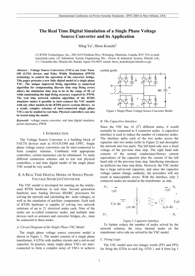
The single phase voltage source converter model is shown in Figure 1. The model consists of a single phase transformer, 4 GTOs with snubber circuits and a rail-to-rail capacitor. In practice, many single phase VSCs are inter-connected to form a complex array of VSCs to achieve
certain goals.
Figure 1 Single Phase Voltage Source Converter Model
B. The Capacitive Interface
Since the VSC has 16 (24) different states, it would normally be connected to 4 connector nodes. A capacitive interface is used to reduce the number of connector nodes. The interface splits each of the two nodes across the capacitor into two nodes (refer to Figure 2) and decouples the network into two parts. The left hand side sees a fixed voltage of the previous time step. The right hand side consists of the normal conductance/history current equivalence of the capacitor plus the current of the left hand side of the previous time step. Interfacing introduces an artificial one time step delay. However, the VSC model has a large rail-to-rail capacitor, and since the capacitor voltage cannot change suddenly, the procedure will not result in unacceptable errors. With the interface, only 2 connector nodes are needed at the transformer ac side. N1 N’1
i1(t) i2(t) +
Vc(t) gc Vc(t-�t)Ihc(t-�t) i2(t-�t) -
N2
N’2
Figure 2. Capacitive Interface To further reduce the number of nodes solved by the
network solution, the two� internal nodes on the transformer valve side are solved by the VSC model.
C. Firing Logic
The VSC model uses two integer words (FP1 and FP2) for firing the GTOs in each leg. GTO 1 and 4 form leg 1
1

International Conference on Power Systems Transients - IPST 2003 in New Orleans, USA
III. APPLICATIONS OF THE SINGLE PHASE VOLTAGE SOURCED CONVERTER
while GTO 3 and 2 form leg 2. The firing control words can either come from a PWM controller simulated on the RTDS or from a real physical controller connected to its inputs. When a binary firing control word is 00, neither of the two GTOs in the leg are conducting. When the firing control word value is 01 or 11, the upper GTO is conducting, and when it is 10, the bottom GTO is conducting. Diodes conduct whenever positively biased. The binary firing control word value of 11 is not permitted to fire both the top and the bottom GTOs at the same time, since it would then short-circuit the rail-to-rail capacitor.
A. Simulation Models and Parameters of Two Level Vic’s
The single-phase VSC models combined with a control system were tested and their behavior was compared with EMTDC equivalents. The diagram of the simulation model is shown in Figure 5. Two single-phase VSC models are connected in series on both ac and dc side.
The control system consists of two controllers. One is a
dc voltage controller (AVdR) which commands the phase angle reference of the VSC output ac voltage and the other is an ac voltage controller (AVaR) which commands the magnitude reference of the VSC output ac voltage. Both controllers consist of a feedback controller with PI control. The phase angle difference of ac output voltage of each VSC model are 60 electrical degrees to decrease harmonics of the VSC output. The parameters of the models in the simulation are listed in Table 1.
D. Improved Firing
The typical simulation time step of the RTDS is about 50 �S. Without improved firing, the maximum error of firing pulse arrival time would be 25 �S, representing roughly 0.5�. Any firing error causes uneven capacitive voltage peaks and harmonics in the simulation results which do not exist in the real system. With a PWM controller, the valves are switched on and off many times per cycle, making the firing error more significant. When many VSC bridges are inter-connected, the problem becomes even worse.
To compensate for the discrete time step firing error, an
improved firing algorithm unique to RTDS is used in the VSC model.
Figure 3. Capacitor voltage without improved firing
In addition to the normal firing pulse word, the improved firing algorithm requires a fractional signal indicating the exact arrival time of the firing pulse. The algorithm uses the fractional signal to modify the capacitor voltage by removing electric charge from the capacitor for the period in which the GTO should have been off or by adding electric charges to the capacitor for the period in which the GTO should have been on.
AvdR: DC voltage controllAvaR: AC voltage controllPWM: PWM pulse generat
Figure 5. Multi-connected Single-phase V
The same simulation models and pafor both the RTDS and EMTDC simutime step is 50 �s in the case of RTDS anof EMTDC. Steady state STATCOM voltage drops of 10% for 70 ms are analy
The fractional signal can come from either a controller simulated on the RTDS or a real physical controller with the help of a Digital Input Time Stamp card – special hardware designed to measure the accurate arrival time of firing pulses.
Table 1 Parameters of the Single-phase V
AC system 230 kAC system impedance 0.12 HConverter transformer 233.8Rated DC voltage �X��Snubber circuit 1.5�FDC capacitor 250 �PWM carrier frequency 180 HRTDS simulation time step 50 �SEMTDC simulation time step 5 �S
Figure 4. Capacitor voltage with improved firing
2
+-
er er or SC Test Circuit
rameters are used lation, except the d 5 �s in the case operation and ac zed.
SC Test Circuit
V / 60 Hz + 1 �
MVA, 20%Z � kV , 100 � F z

International Conference on Power Systems Transients - IPST 2003 in New Orleans, USA
B. Simulation Results C. Simulation Models of Multilevel VSCs
Figure 6 shows the steady state STATCOM operation. The 4 traces in each of 4 figures show DC voltage (Vdc or Vdct, please refer to Fig.5), GTO current of both the positive dc voltage side of the converter bridge (Idp) and the negative dc voltage side (Idn), VSC output ac voltage (Vac), and ac current on ac source side (Iac). Figure 6(a) and 6(c) show the waveforms produced by RTDS simulation and Figure 6(b) and 6(d) show waveforms produced by EMTDC simulation. In these figures, 6(a) and 6(b) show behavior of the upper single-phase VSC model while 6(c) and 6(d) show that of the lower single-phase VSC model. Please note that the reference directions of GTO current is opposite for RTDS simulation and EMTDC simulation in the figures. System behavior simulated by the RTDS and EMTDC are very close. Magnitude of the VSC output ac voltage from the RTDS is about 10% higher than that of the EMTDC, as shown between figure 6(a) and 6(b) and between figure 6(c) and 6(d). This error arises in part because the time step of the RTDS simulation is 10 times larger than the time step of the EMTDC simulation and approximation were made to facilitate the interface.
Analysis of two level VSCs has been extended to chain link converter models consisting of six single phase VSC models in series on AC side and DC side, shown in Figure 8 [2],[3]. Low harmonics in AC voltage are expected for the models regardless of low carrier frequency and therefore low converter losses. We are constructing and adjusting the system parameters using RTDS to confirm these merits.
Figure 7 shows the behavior when the AC voltage is
reduced to 10% for 70 ms. System behaviour of the RTDS and EMTDC simulation are very close. Differences are similar to that of the steady state analysis described above. Figure 8. Chain link converter application
Figure 6(b) Results of EMTDC simulation (5�S)
Figure 6(a) Results of RTDS simulation (50�S)
3

International Conference on Power Systems Transients - IPST 2003 in New Orleans, USA
Figure 6(c) Results of RTDS simulation (50�S) Figure 6(d) Results of EMTDC simulation (5�S)
Figure 7(a) Results of RTDS simulation (50�S) Figure 7(b) Results of EMTDC simulation (5�S)
4

International Conference on Power Systems Transients - IPST 2003 in New Orleans, USA
5
Figure 7(c) Results of RTDS simulation (50�S) Figure 7(d) Results of EMTDC simulation (5�S)
VI. CONCLUSIONS
Finally, it can be concluded that the simulation model of the RTDS single phase VSC is suitable for real time system dynamic studies and tests. The improved firing algorithm can effectively compensate for the discrete time step firing error.
REFERENCES [1] P.G. McLaren, R. Kuffel, R. Wierckx, J. Giesbrecht, L. Arendt,
“A real time digital simulator for testing relays”, IEEE Trans. PWRD, Vol.7, No. 1, pp. 207- 213, Jan. 1992
[2] Konishi H, Sugimoto S, Ogawa S, “Performance study of a chain link converter application in Back-To-Back and HVDC systems”, ICEE'2001, Proceedings, pp606-609, July 22-26 2001
[3] Konishi H, Sugimoto S, Verma S, Ogawa S, “DC voltage control for HVDC system composed of chain link converters,” ICEE'2002, Proceedings Vol. V, pp2109-2113, July 7-11 2002
[4] H.W. Dommel, “Digital computer solution of electromagnetic transients in single- and multi-phase networks,” IEEE Trans., Power App. and Syst., Vol. PAS-88 (4), pp. 388-398, 1969.
[5] Narain G. Hingorani, Laszlo Gyugyi, “Understanding FACTS: concepts and technology of flexible AC transmission systems,” IEEE Press, 1999