The PWM Strategies of Grid-connected Distributed ...
8
The PWM Strategies of Grid-connected Distributed Generation Active NPC Inverters Lin Ma Beijing Jiao Tong University No.3 of Shangyuan Residence Haidian District, 100044 Beijing, China [email protected] [email protected] Xinmin Jin Beijing Jiao Tong University No.3 of Shangyuan Residence Haidian District, 100044 Beijing, China [email protected] Tamas Kerekes Member, IEEE Aalborg University Pontoppidanstraede 101 9220 Aalborg East Aalborg, Denmark [email protected] Marco Liserre Dipartimento di Elettrotecnica ed Elettronica Politecnico di Bari E. Orabona 4-70125 Bari, Italy [email protected] Remus Teodorescu Senior Member, IEEE Aalborg University Pontoppidanstraede 101 9220 Aalborg East Aalborg, Denmark [email protected] Pedro Rodriguez IEEE Department of Electrical Engineering Technical University of Catalonia Barcelona, Spain [email protected] Abstract -- The Neutral Point Clamped topology due to high efficiency, low leakage current and EMI, its integration is widely used in the distributed generation (DG) systems. However the main disadvantage of the NPC inverter is given by an unequal distribution of the losses in the semiconductor devices, which leads to an unequal distribution of temperature. By using the Active NPC topology, the power losses distribution problem is alleviated. The modulation strategy is a key issue for losses distribution in this topology. In this paper two known strategies are discussed and a new proposed PWM strategy, namely the Adjustable Losses Distribution (ALD) PWM strategy is proposed for better losses distribution in the Active NPC (ANPC) topology. Simulations using Simulink and the PLECS toolbox have been done for evaluating efficiency of different NPC topologies and some experimental results are presented in this paper to validate the operation of the different strategies. Index Terms -- Multilevel systems, Photovoltaic power systems, Pulse modulation, Topology I. INTRODUCTION With the renewable power increasing, the grid-connected photovoltaic (PV) systems, in particular low power single- phase systems (from 1kW to 10kW), are becoming one of the most important parts in the DG (Distributed Generation) system. Meanwhile the low power PV systems are usually private systems, which need to give the users maximum profitability through high efficiency, long life time, low prices, small volume and safety. In order to improve the efficiency of PV inverters and lower the system prices, the grid isolation transformers are usually eliminated (they are usually used for providing personal protection and avoiding leakage currents between the PV system and the ground). Thereby, many transformerless applications were proposed [1] including HERIC topology [2], FB with DC Bypass topology [3], H5 topology [4], conventional Neutral Point Clamped (NPC) topology, Conergy NPC topology and Active NPC topology. The NPC topology was introduced by Nabae, Takahashi and Akagi in 1981 [5], it was one of the inverter topologies connecting to the grid without using any transformer. Compared with the traditional 2-level full bridge PWM inverters, the NPC topology also can produce lower switch losses, harmonics and common mode current which significantly improve the efficiency of the inverters and make it appealing for photovoltaic application. Meanwhile the main disadvantage of the NPC inverter is given by an unequal distribution of the losses in the semiconductor devices, which leads to an unequal distribution of temperature and limits the output power of the inverter. In order to overcome this drawback, the conventional NPC topology was extended to the Active NPC structure. The Active NPC has more degrees of freedom and can be controlled by different PWM strategies. Compared to the conventional NPC topology, the total losses in 3L-ANPC converter are not smaller, but a better balancing of losses is obtained. Lots of different Active NPC PWM strategies have been presented in [6] [7], but the losses distribution was not ideal because conduction loss distribution is not equal and will be influenced by the work mode. In this paper, two known PWM strategies for ANPC are shown and a new PWM strategy named Adjustable Losses Distribution (ALD) for better losses distribution is proposed. This PWM strategy could get loss balanced by adjusting the switching losses distribution. The comparison and control strategies of different strategies are also discussed. After showing some simulation and experimental results, a conclusion is given which proves that the proposed strategy has better losses distribution performance. 920 978-1-4244-2893-9/09/$25.00 ©2009 IEEE
Transcript of The PWM Strategies of Grid-connected Distributed ...

The PWM Strategies of Grid-connected Distributed Generation Active NPC Inverters
Lin Ma
Beijing Jiao Tong University No.3 of Shangyuan Residence
Haidian District, 100044 Beijing, China
[email protected] [email protected]
Xinmin Jin
Beijing Jiao Tong University No.3 of Shangyuan Residence
Haidian District, 100044 Beijing, China
Tamas Kerekes Member, IEEE
Aalborg University Pontoppidanstraede 101
9220 Aalborg East Aalborg, Denmark
Marco Liserre Dipartimento di Elettrotecnica ed
Elettronica Politecnico di Bari E. Orabona 4-70125
Bari, Italy [email protected]
Remus Teodorescu Senior Member, IEEE
Aalborg University Pontoppidanstraede 101
9220 Aalborg East Aalborg, Denmark
Pedro Rodriguez IEEE Department of Electrical
Engineering Technical University of Catalonia
Barcelona, Spain [email protected]
Abstract -- The Neutral Point Clamped topology due to high efficiency, low leakage current and EMI, its integration is widely used in the distributed generation (DG) systems. However the main disadvantage of the NPC inverter is given by an unequal distribution of the losses in the semiconductor devices, which leads to an unequal distribution of temperature. By using the Active NPC topology, the power losses distribution problem is alleviated. The modulation strategy is a key issue for losses distribution in this topology. In this paper two known strategies are discussed and a new proposed PWM strategy, namely the Adjustable Losses Distribution (ALD) PWM strategy is proposed for better losses distribution in the Active NPC (ANPC) topology. Simulations using Simulink and the PLECS toolbox have been done for evaluating efficiency of different NPC topologies and some experimental results are presented in this paper to validate the operation of the different strategies.
Index Terms -- Multilevel systems, Photovoltaic power systems, Pulse modulation, Topology
I. INTRODUCTION With the renewable power increasing, the grid-connected
photovoltaic (PV) systems, in particular low power single-phase systems (from 1kW to 10kW), are becoming one of the most important parts in the DG (Distributed Generation) system. Meanwhile the low power PV systems are usually private systems, which need to give the users maximum profitability through high efficiency, long life time, low prices, small volume and safety.
In order to improve the efficiency of PV inverters and lower the system prices, the grid isolation transformers are usually eliminated (they are usually used for providing personal protection and avoiding leakage currents between the PV system and the ground). Thereby, many transformerless applications were proposed [1] including HERIC topology [2], FB with DC Bypass topology [3], H5 topology [4], conventional Neutral Point Clamped (NPC) topology, Conergy NPC topology and Active NPC topology.
The NPC topology was introduced by Nabae, Takahashi and Akagi in 1981 [5], it was one of the inverter topologies connecting to the grid without using any transformer. Compared with the traditional 2-level full bridge PWM inverters, the NPC topology also can produce lower switch losses, harmonics and common mode current which significantly improve the efficiency of the inverters and make it appealing for photovoltaic application.
Meanwhile the main disadvantage of the NPC inverter is given by an unequal distribution of the losses in the semiconductor devices, which leads to an unequal distribution of temperature and limits the output power of the inverter. In order to overcome this drawback, the conventional NPC topology was extended to the Active NPC structure.
The Active NPC has more degrees of freedom and can be controlled by different PWM strategies. Compared to the conventional NPC topology, the total losses in 3L-ANPC converter are not smaller, but a better balancing of losses is obtained. Lots of different Active NPC PWM strategies have been presented in [6] [7], but the losses distribution was not ideal because conduction loss distribution is not equal and will be influenced by the work mode.
In this paper, two known PWM strategies for ANPC are shown and a new PWM strategy named Adjustable Losses Distribution (ALD) for better losses distribution is proposed. This PWM strategy could get loss balanced by adjusting the switching losses distribution. The comparison and control strategies of different strategies are also discussed. After showing some simulation and experimental results, a conclusion is given which proves that the proposed strategy has better losses distribution performance.
920978-1-4244-2893-9/09/$25.00 ©2009 IEEE

II. CONVENTIONAL NPC TOPOLOGY
Fig. 1. Neutral Point Clamped Half Bridge
The conventional NPC topology is the most popular 3-
level topology. It is also very versatile and can be used in both single phase (full-bridge or half-bridge) and three-phase inverters. As presented in Fig.1, the NPC half bridge is composed by four switches and two clamp diodes. The main concept is that zero voltage can be achieved by “clamping” the output to the grounded “middle point” of the dc bus using D+ or D- depending on the sign of the output current.
Fig.2 shows the switching losses of a 5kW NPC topology inverter at different switching frequencies which presents the losses distribution is unbalance. This figure points out that the stresses due to switching losses on the outer switches S1 and S4 is higher than on the inner switches, especially at higher frequency (Fig.2b). As the switching frequency increases, the uneven losses distribution in the NPC inverter gets even worse.
For a PV system, the modulation index is often fixed when the DC bus and the grid voltage are given and the power factor also fixed at PF=1. The modulation index of a full bridge power converter is usually set around M=0.9 with DC bus voltage VDC=400V and grid AC voltage 230V (RMS).
In this paper, without lost of generality, power losses distribution is studied in half bridge topologies with a DC bus voltage of VPV=800V and a 220V (RMS)/50Hz AC grid voltage. The passive components are the same for all the simulated topologies. The switch model is based on the MITSUBISHI PM75DSA120 intelligent power module (IPM). The power rate is set to 5kW for simulation purposes. The switching frequencies are set to 10kHz and 16kHz (the commercial PV inverters normally use 16kHz, but 10kHz was used in the lab experiments).
As Fig.2 shows, the stress due to the total switching losses is stronger in the outer IGBTs (S1 and S4) than in the inner ones (S2 and S3). The conduction losses distribution is dependant of the modulation index (M). When M=1, the outer IGBTs exhibit the highest conduction losses stress. As both the conduction and switching losses overstress the outer IGBTs (S1, S4) respect the inner ones (S2, S3), the unbalanced losses distribution restricts the system power rate
in case of high power applications.
Fig. 2. Switching losses of a 5kW NPC topology inverter at different
frequencies, M=0.9 and PF=1
III. ACTIVE NPC TOPOLOGY AND ITS PWM STRATEGIES
Fig. 3. Active Neutral Point Clamped Half Bridge
The ANPC topology inverter [8] is derived from the conventional NPC topology as presented in Fig.3. Two active switches with anti-parallel diodes are used for clamping.
The ANPC topology, in contrast to the conventional NPC converter, has more than one way to clamp the midpoint. The upper clamping path results from turning on S2 and S5 and the lower clamping path from turning on S3 and S6. The current can be conducted through both clamping ways in both
(b) Switching frequency at 16 kHz
(a) Switching frequency at 10 kHz
921
directions. The distribution of the conduction losses during the zero states can be controlled by the selection of the different NPC paths. The switching losses could be controlled by the selection of different commutation states.
There are many different PWM strategies for Active NPC control by using different zero states and conduction paths [7]. In this section, two PWM strategies are introduced, and a new PWM strategy named Adjustable Losses Distribution (ALD) is proposed.
A. Classical Active PWM Strategies In [7], the PWM-1 and PWM-2 strategies for Active NPC
are discussed. In the case of the PWM-1 strategy, the inner switches have only conduction losses and the switching losses mainly stress the outer IGBTs. In the case of PWM-2 the strategy, the mainly switching losses only stress the inner switches. The power losses distribution situation is not improved in the PWM-1 strategy and gets even worse in the PWM-2 strategy compared with conventional NPC topology. The efficiency was also not changed compared with the conventional NPC topology.
B. DF-ANPC Strategy Papers [7], [8] show a PWM strategy named Double-
Frequency ANPC control which naturally doubles the apparent switching frequency. In comparison with the other ANPC PWM strategies, the DF-ANPC strategy has four zero states: 0+1, 0+2, 0-1 and 0-2 (Table I). For the zero voltage states, different control sequences could be used with different losses distribution needs.
The reference voltage is compared with two carrier waves that are phase-shifted by Ts/2. As there are two active states in a half cycle, this ANPC control strategy naturally doubles the apparent switching frequency. As there are two positive and two negative active states during one switching period, the output voltage has an apparent switching frequency equal to 2fs.
TABLE I SWITCHES STATES OF DF-ANPC HALF BRIDGE INVERTER S1 S2 S3 S4 S5 S6
Positive 1 1 0 0 0 10+1 0 1 0 0 1 00+2 1 0 1 0 0 10-2 0 1 0 1 1 00-1 0 0 1 0 0 1
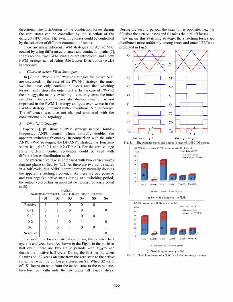
Negative 0 0 1 1 1 0The switching losses distribution during the positive half
cycle is analyzed here. As shown in the Fig.4, in the positive half cycle, there are two active periods with VAO=VPV/2 during the positive half cycle. During the first period, when S1 turns on, S2 keeps on state from the zero state to the active state, the switching on losses stresses on S1. When S2 turns off, S1 keeps on state from the active state to the zero state, therefore S2 withstands the switching off losses stress.
During the second period, the situation is opposite, i.e., the S2 takes the turn on losses and S1 takes the turn off losses.
By means this switching strategy, the switching losses are distributed more uniformly among inner and outer IGBTs as presented in Fig.5.
1S
2S
3S
4S
Sr
ABV
0 0Sr
0
0
5S
6S
1S
2S
3S
4S
ABV
5S
6S
Fig. 4. The switches states and output voltage of ANPC-DF strategy
Fig. 5. Switching losses of a 5kW DF-ANPC topology inverter
(a) Switching frequency at 5kHz
(b) Switching frequency at 8kHz
922
Compared with the conventional NPC topology, the efficiency does not improve. However, the power losses distribution problem is improved by using the ANPC control strategy.
C. Adjustable Losses Distribution (ALD) ANPC strategy
1S
2S
3S
4S
'Sr
ABV
5S
6S
1S
2S
3S
4S
ABV
5S
6S
0 0
0 0
Sr'Sr
Sr
VPV
/2
VPV
/2
1S
2S
3S
4S
ABV
5S
6S
1S
2S
3S
4S
ABV
5S
6S
0 0
0 0
'SrSr
'SrSr
Fig. 6. The switches states and output voltage of ALD strategy
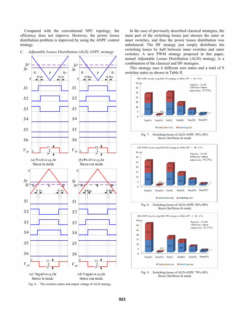
In the case of previously described classical strategies, the main part of the switching losses just stresses the outer or inner switches, and thus the power losses distribution was unbalanced. The DF strategy just simply distributes the switching losses by half between inner switches and outer switches. A new PWM strategy proposed in this paper, named Adjustable Losses Distribution (ALD) strategy, is a combination of the classical and DF strategies.
This strategy uses 6 different zero states and a total of 8 switches states as shown in Table II.
Fig. 9. Switching losses of ALD-ANPC 70%-30%Stress Out/Stress In mode
Fig. 8. Switching losses of ALD-ANPC 60%-40%Stress Out/Stress In mode
Fig. 7. Switching losses of ALD-ANPC 50%-50% Stress Out/Stress In mode
923
When the switching sequence follows as 0+, 0+In, Positive, 0+In, 0+ or 0-, 0-In, Negative, 0-In, 0- as shown in the Fig.6 (a) and (c), named Stress In mode, the switching losses stress the inner IGBTs, since the outer switches make zero current switching (ZCS) whereas the inner switches make hard switching (HS).
TABLE II SWITCHES STATES OF ALD-ANPC HALF BRIDGE INVERTER
S1 S2 S3 S4 S5 S6
Positive 1 1 0 0 0 10+In 1 0 1 0 0 1
0+Out 0 1 1 0 0 10+ 0 0 1 0 0 10- 0 1 0 0 1 0
0-Out 0 1 1 0 1 00-In 0 1 0 1 1 0
Negative 0 0 1 1 1 0 When the switching sequence follows as 0+, 0+Out,
Positive, 0+Out, 0+ or 0-, 0-Out, Negative, 0-Out, 0- as shown in the Fig.6 (b) and (d), named Stress Out mode, the
switching losses stress on the outer IGBTs, since the inner switches make ZCS whereas the outer switches make HS.In a given cycle, we can choose the different working time rates of Stress In mode and Stress Out mode to modify the switching losses distribution as shown in Fig.10. If the conduction losses are mainly stressed inner IGBTs (the conduction losses distribution are depending on the modulation index M and power factor PF), then the ALD control could give more switching losses to outer IGBTs by increasing the rate of Stress Out mode. Thereby, the total losses of inner and outer IGBTs are balanced. Otherwise, if the conduction losses are mainly stressed outer IGBTs, then it could give more switching losses to outer IGBTs by increasing the rate of Stress In mode.
Some simulation results are shown in Fig.7, 8 and 9. For 50%-50% Stress In/Stress Out mode (Fig.7), the total losses of S1/D1 and S2/D2 are 22.3W and 37.2W respectively, the losses distribution between outer and inner switches is not ideal. For 40%-60% Stress In/Stress Out mode (Fig.8), the losses distribution is improved to: 24.8W and 34.6W respectively. For 30%-70% Stress In/Stress Out mode (Fig.9), the losses distribution is balanced to 30.1W and 29.2W. By using this strategy, the power losses distribution problem could be alleviated.
Fig. 10. Stress In mode and Stress Out mode selection during positive half cycle (turn off)
924

D. The PWM Generation of Adjustable Losses Distribution (ALD) ANPC Strategy
The ALD Pulse Width Modulation generation method is shown in the Fig.6 and Fig.11. Fig.6 shows one switching cycle, whereas Fig.11 shows two grid cycles, the first one with 50%-50% Stress In/Stress Out mode and the second one with 30%-70% Stress In/Stress Out mode.
S1/S4
S2/S3
S5/S6
50% Stress In mode25% Stress Out mode 30% Stress In mode
35% Stress Out mode25% Stress Out mode
35% Stress Out mode
Sr (modulation wave with adding signal)
Sr (original modulation wave )
Stress Out mode
Stress In mode Fig. 11. PWM generation for one cycle of 50%-50% Stress In/Stress Out
mode and one cycle of 30%-70% Stress In/Stress Out mode
As shown in Fig.11, in order to distribute the switching losses between S1 and S4 equally during the first grid cycle (50%-50% Stress In/Stress Out mode), S1 takes first 25% positive Stress Out mode switching losses and S4 takes the another 25% negative Stress Out mode. The Stress In mode is also shared by positive and negative cycle equally in order to S2 and S3 take the same switching losses.
During the Stress In mode, a new modulation signal Sr’ is composed by a synchronized sinusoidal wave signal added to the S1/S4 modulation wave Sr. In the experiments, the amplitude of this adding wave is 10% of the modulation wave. During the Stress Out mode, this signal wave is added to the S2/S3 modulation wave Sr. S5 and S6 switch at grid frequency (see Fig.6 and Fig.11).
When Stress In mode is used, during the positive half cycle, S1 uses signal Sr’ instead modulation signal Sr whereas during the negative half cycle, S4 uses Sr’ instead Sr. When Stress Out mode is used, during the positive half cycle, S2 uses Sr’ whereas during the negative half cycle, S3 uses Sr’ instead Sr. It’s also illustrated by Fig.6.
By using this strategy, the amplitude of Sr’ could exceed the amplitude of the carrier for a period, which means that the state of inner switches or outer switches (depending on Stress
In mode or Stress Out mode) will not be changed during this period. In the case of positive active state, S1 and S2 must be ON at the same time, the same situation with the S3 and S4 in the case of negative active state. For example, using Stress In mode during the positive half cycle, S1 keeps ON if the amplitude of Sr’ exceed the amplitude of carrier. However, this does not influence the output current, since the state of S1 neither influences the active state nor changes the modulation index. The duration of the both switches ON states is not changed. Therefore the modulation index will not be changed (see Fig.12).
Plots of Fig.12 demonstrate that the over range of Sr’ does not influence the output current. Fig.12 shows how the Stress Out mode is used during the negative half cycle. In Fig.12 (a), no signal is added to the original modulation wave. In Fig.12 (b), a 10% signal (which means the amplitude of adding signal is 10% to the amplitude of the Sr) is added to the modulation wave (S2/S3) Sr to get Sr’. In Fig.12 (c), a 100% signal is added to the modulation wave, therefore it easy to find that S2 keeps OFF states for a long period because of the over range of Sr’. Fig.12 validates that the over range of Sr’ does not influence the output current.
Fig. 12. Experimental waveform
(Ch1 Output current Ch2 S1 Driver Signal Ch3 S5 Driver Signal Ch4 S2 Driver Signal )
Fig.12 validates that the over range of Sr’ does not
influence the output current. During the zero states 0+out and 0-out using Stress Out mode, there are two paths the current could pass through (Fig.10), which means that the conduction losses could be taken by S2/D5 and S3/S6 or S2/S5 and S3/D6 during this period. For ALD, another advantage is that it could choose the better path and gets the lower conduction
925

loss depend on IGBT and anti-parallel diode’s conduction voltage drop naturally during the zero states 0+out and 0-out (Fig.10). If the IGBT’s threshold voltage higher than the diode’s, then during the positive half cycle the current will choose the D5 and S2 path as VBN is clamped by D5 and S2, S6 and S3 cannot turn on (or the conduction current is very small), otherwise if the diode’s threshold voltage higher than the IGBT’s, then D5 and S2 block the current. Whatever when D5 and S2 block the current, as the voltage VBA>0 (positive half cycle), there is also some current passed by. It’s better turn off S2 as soon as possible. Which means if the Diode’s threshold voltage bigger than IGBT’s, it’s better add a small adding signal (Fig.12). In experiment, 10% additional signal was used.
This method also could use the dead time as an additional mode. As Fig.12 shown, in the positive half cycle, S1/S4 is naturally turns on and off before S2/S3 because of the dead time setting. It could be understood as a Stress In mode.
The main features of this ANPC converter with ALD strategy are:
• It is possible to control the switching losses distribution by controlling the adding sine wave.
• There are six zero states in the current switching process.
• The adding sine wave has same phase angle and frequency as the modulation wave.
• It is easy to control the switching distribution, since just one parameter needs to be modified.
• It is able to balance the power losses between the outer and the inner switches by distributing switching losses.
• The efficiency of different Stress In/Stress out rate ALD strategy is the same.
• The total losses of inner switches S2/S3 may be different caused by the 0-out and 0+out zero states. If the clamped period of Stress Out mode is long, the unbalance will get worse.
IV. EXPERIMENTAL RESULTS The experimental tests setup is constructed by
MITSUBISHI PM75DSA120 intelligent power modules (IPM) and the system parameters are shown in Table III. The YOGOGAWA WT3000 Precision Power Analyzer is used for calculating the efficiency of the different inverters.
Due to the fact that the IPM used in the experiments encases two IGBTs of a single leg, the power losses distribution cannot be measured in each single switch. Therefore the experimental results are focused on evaluating the conversion efficiency of the tested topologies. These experiments reveal that overall efficiency of the Active NPC and the conventional NPC topologies are quite similar, independently of the modulation strategy (PWM-1, PWM-2, DF, and ALD).
Fig. 13. Experimental equipments
In simulation, the inductor losses were neglected. In the
experiments however, the overall efficiency got 0.45% lower when a second 2mH inductor was added to the original 2mH output filter (total 4mH).
In simulation, as shown in Fig. 3, the efficiency of the NPC was 97.64% from simulation (neglecting the filter losses). If the estimated filter losses are included (0.45%),
TABLE IVEFFICIENCY EXPERIMENTAL RESULTS
Input Power (kW) 0.5kW 1.0kW 1.5kW 2.0kW 2.5kW 3.0kW 3.5kW 4.0kW 4.5kW
NPC Efficiency (%) 94.98 95.87 96.38 96.71 96.85 97.06 97.17 97.25 97.23
Conergy NPC Efficiency (%) 95.34 96.18 96.62 97.05 97.14 97.42 97.47 97.60 97.67
DF Active NPC Efficiency (%) 94.60 95.82 96.35 96.72 96.94 97.08 97.20 97.29 97.34
ALD Active NPC Efficiency (%) 94.45 95.67 95.16 96.53 96.70 96.86 97.03 96.14 97.22
926

then the efficiency decreases to 96.2%, which matches the experimental results detailed in Table IV.
TABLE III SYSTEM PARAMETERS
Quantity Value Comment
Line frequency 50Hz
Carrier frequency 10kHz DF Active NPC 5kHz
Output filter L 2mH CDC 1000uF Each level Rated DC voltage 800V 400V each level RLoad 15Ω Switches PM75DSA120 MITSUBISHI IPM
Fig. 14. Efficiency curves
From the experiments, the efficiency curves for the tested
topologies are given in Fig.14. The efficiencies of the Active NPC and conventional NPC are almost equal. In fact, the efficiency of inverter by using different Active NPC PWM strategies should be same. Because of the experimental environment changed, the efficiency is changed slightly. The difference is focused on the lost distribution.
V. CONCLUSION The NPC topology showed very high performances both in
the experimental and the simulation tests conducted in this work, which make them very suitable for transformer-less PV applications due to their high efficiency and low leakage current and EMI. Whereas the main disadvantage of the NPC inverter is given by an unequal distribution of the losses in the semiconductor devices, which leads to an unequal distribution of temperature and limits the output power of the inverter. In order to overcome this drawback, the conventional NPC topology was extended to the Active NPC structure.
The ANPC topology, which uses different modulation strategies, has a better power losses distribution. Thus, the ANPC topology is suitable for the high power transformer-less PV system applications. The modulation strategy is a key issue in this topology. As S1 and S5, S4 and S6, S2 and S3
(active states) could not be ON at the same time (see Fig.6), the dead time setting needs to be carefully considered.
In this paper, a new ANPC strategy named Adjustable Losses Distribution (ALD) is proposed. This strategy combines the losses distribution advantages of classical and DF-ANPC strategies. Depending on the different M and PF (which means different conduction losses distribution between inner and outer switches), this strategy can choose the most suitable Stress In/Stress Out mode rate to balance the total losses distribution between inner and outer switches, where the switching losses distribution is controlled by the Stress In/Stress Out mode rate. This strategy is validated by experiments that the efficiency is not lower compared with other ANPC strategies. The simulation results show that whatever the M and PF value are, the losses distribution could get balanced without adding any components.
The NPC topology is currently used by Danfoss Solar Inverters in a three-phase configuration with multi-string boost converter. With the power rate of DG systems increasing, Active NPC topology and ALD strategy might be widely used in particular high power systems.
REFERENCES [1] Kerekes, T. Teodorescu, R. and Borup, U, “Transformerless
Photovoltaic Inverters Connected to the Grid [C],” Applied Power Electronics Conference, APEC 2007 - Twenty Second Annual IEEE, Feb.25.2007-March.1.2007, Page(s):1733-1737.
[2] Schmidt, Heribert – European Patent Application, Pub No.03009882.6, Pub. Date: 15.05.2003
[3] Gonzalez, R.; Lopez, J.; Sanchis, P.; Marroyo, L, ‘Transformer-less Inverter for Single-Phase Photovoltaic Systems [J]’, Power Electronics, IEEE Transactions on Volume 22, Issue 2, March 2007, Page(s):693 – 697.
[4] Matthias Victor – United States Patent Application, Pub No.US2005/0286281 A1, Pub. Date: 29 Dec 2005
[5] A. Nabae, I. Takahashi, and H. Akagi, “A new neutral-point-clamped PWM inverter [J],” IEEE Trans. Ind. Applicat., vol. 17, Page(s): 518–523, Sep./Oct. 1981
[6] Knaup P – International Patent Application, Pub No. WO 2007/048420 A1, Pub. Date: 3 May 2007
[7] D. Floricau, E. Floricau and M. Dumitrescu; “Natural Doubling of the Apparent Switching Frequency using Three-Level ANPC Converter [C]”, Nonsinusoidal Currents and Compensation, 2008. ISNCC 2008. International School on 10-13 June 2008 Page(s):1 – 6
[8] Thomas Brückner, Steffen Bernet and Peter K. Steimer, “The Active NPC Converter for Medium-Voltage Applications [C]”, industry Applications Conference, 2005. Fourtieth IAS Annual Meeting. Conference Record of the 2005 Volume 1, 2-6 Oct. 2005 Page(s):84 - 91 Vol.
927