
The Programmable Keyboard /Display Interface...
81
Chapter : 6 The Programmable Keyboard /Display Interface (8279) 1
Transcript of The Programmable Keyboard /Display Interface...
Chapter : 6
The Programmable Keyboard
/Display Interface (8279)
1

Outline
2
Introduction
General Features
Functional Block diagram
Operation Modes
Input mode
Scanned Keyboard mode
Scanned Sensor Matrix mode
Strobed Input mode
Output mode
Left Entry (typewriter type)
Right Entry(calculator type)
Programming the 8279
Introduction
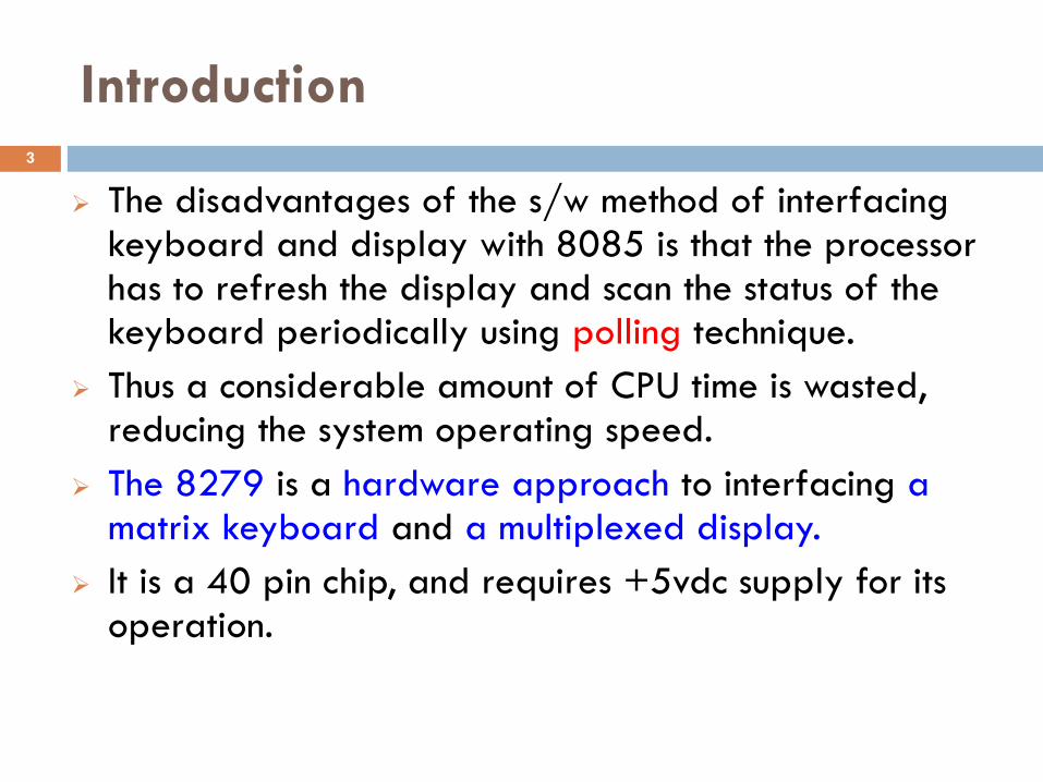
The disadvantages of the s/w method of interfacing
keyboard and display with 8085 is that the processor has to refresh the display and scan the status of the keyboard periodically using polling technique.
Thus a considerable amount of CPU time is wasted, reducing the system operating speed.
The 8279 is a hardware approach to interfacing a matrix keyboard and a multiplexed display.
It is a 40 pin chip, and requires +5vdc supply for its operation.
3

contd.
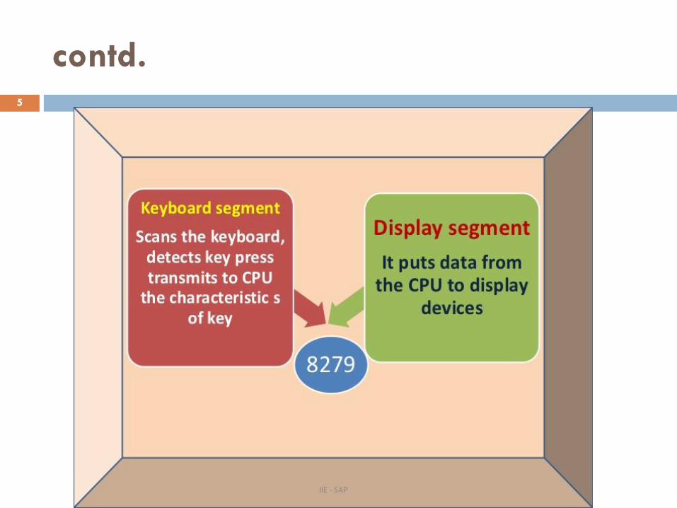
Intel’s 8279 is a general purpose Keyboard
Display controller that simultaneously drives the display of a system and interfaces a Keyboard with the CPU.
The Keyboard Display interface scans the Keyboard to identify if any key has been pressed and sends the code of the pressed key to the CPU. It also transmits the data received from the CPU, to the display device.
4
contd.
5
contd.
6
contd.
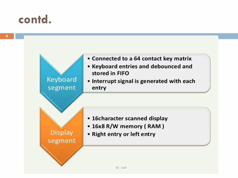
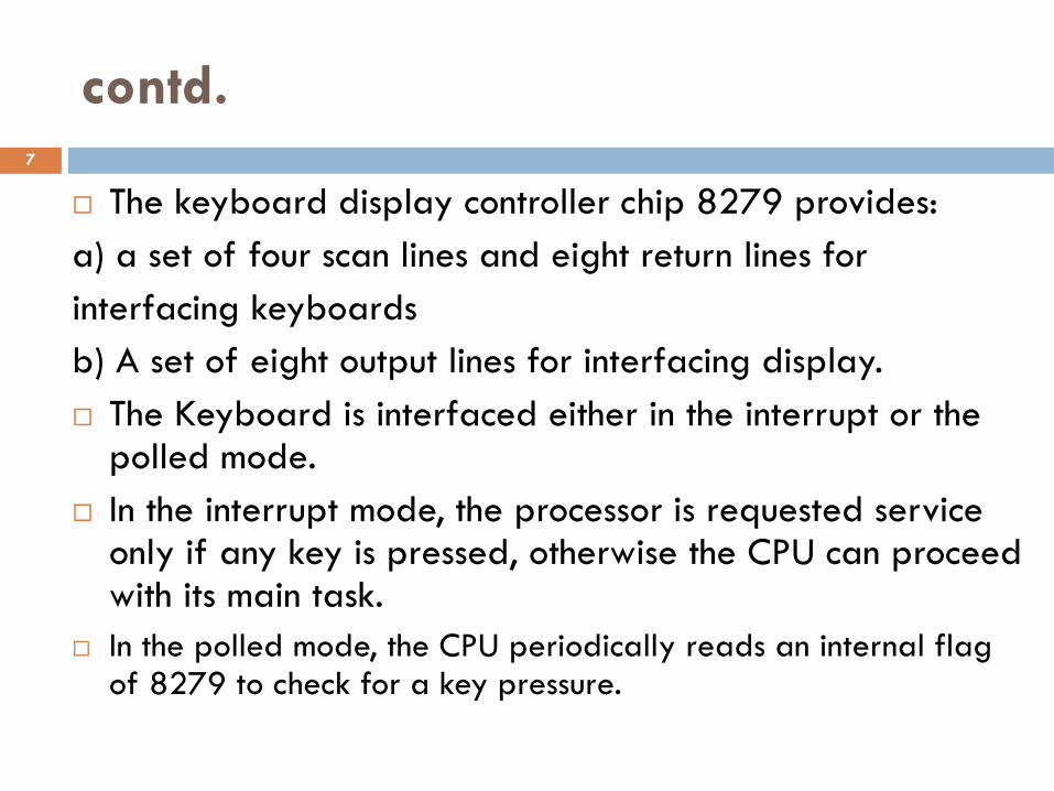
The keyboard display controller chip 8279 provides:
a) a set of four scan lines and eight return lines for
interfacing keyboards
b) A set of eight output lines for interfacing display.
The Keyboard is interfaced either in the interrupt or the polled mode.
In the interrupt mode, the processor is requested service only if any key is pressed, otherwise the CPU can proceed with its main task.
In the polled mode, the CPU periodically reads an internal flag of 8279 to check for a key pressure.
7
contd.
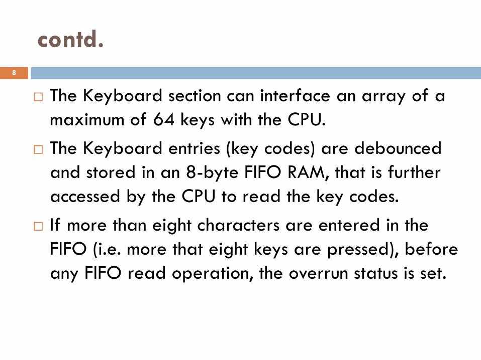
The Keyboard section can interface an array of a
maximum of 64 keys with the CPU.
The Keyboard entries (key codes) are debounced
and stored in an 8-byte FIFO RAM, that is further
accessed by the CPU to read the key codes.
If more than eight characters are entered in the
FIFO (i.e. more that eight keys are pressed), before
any FIFO read operation, the overrun status is set.
8

contd.
If a FIFO contains a valid key entry, the CPU is interrupted
(in interrupt mode) or the CPU checks the status (in polling) to read the entry.
Once the CPU reads a key entry, the FIFO is updated, i.e. the key entry is pushed out of the FIFO to generate space for new entries.
The 8279 normally provides a maximum of sixteen 7-seg display interface with CPU It contains a 16-byte display RAM that can be used either as an integrated block of 16x8-bits or two 16x4-bit block of RAM.
The data entry to RAM block is controlled by CPU using the command words of the 8279.
9

Features of 8279
It is designed by Intel
Simultaneous keyboard and display operation.
It is support 64 contact key matrix with two more keys “CONTROL” and “SHIFT”
Has 3 input operating modes for keyboard interface
1.Scanned keyboard mode
2.Scanned sensor matrix mode
3.Strobed Input mode.
It has inbuilt debounce key .
It provides two output modes:
1.Left entry (Typewriter type).
2.Right entry (Calculator type).
10

Fig. Logic Symbol
Block Diagram of 8279
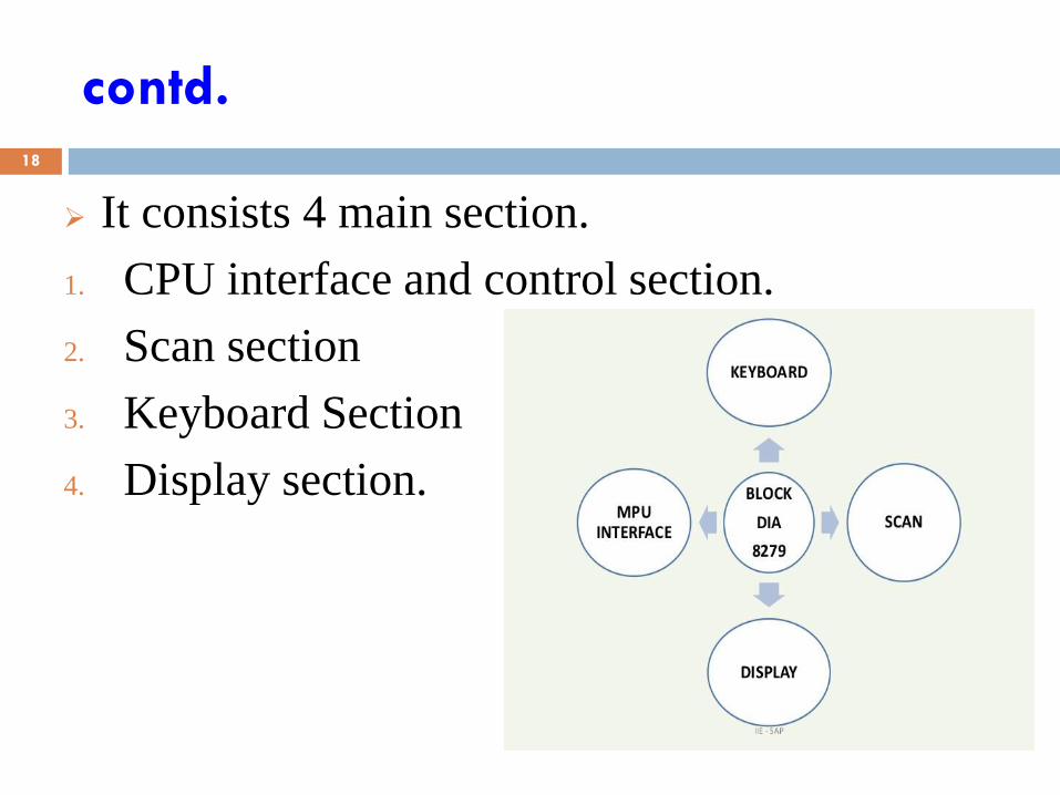
Four major sections:
1. Keyboard
2. Display
3. Scan
4. MPU interface
Fig. Functional Diagram Fig. Pin Configuration

Pin Description
DB7-DB0: These are bidirectional data bus lines.
The data and command words to and from the CPU
are transferred on these lines.
CLK: clock from system used to generate internal
timing.
RESET : This pin is used to reset 8279. A high on
this line resets 8279.
CS chip select: A low on this line enables 8279 for
normal read or write operations. Otherwise this pin
should be high.
12
Pin Description
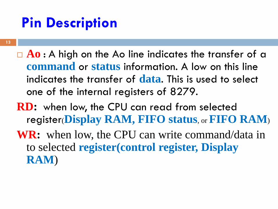
Ao : A high on the Ao line indicates the transfer of a
command or status information. A low on this line indicates the transfer of data. This is used to select one of the internal registers of 8279.
RD: when low, the CPU can read from selected register(Display RAM, FIFO status, or FIFO RAM)
WR: when low, the CPU can write command/data in to selected register(control register, Display RAM)
13
Pin Description
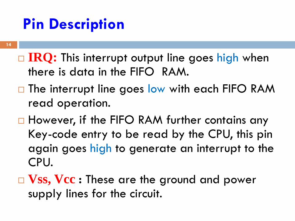
IRQ: This interrupt output line goes high when there is data in the FIFO RAM.
The interrupt line goes low with each FIFO RAM read operation.
However, if the FIFO RAM further contains any Key-code entry to be read by the CPU, this pin again goes high to generate an interrupt to the CPU.
Vss, Vcc : These are the ground and power supply lines for the circuit.
14

Pin Description
SL0-SL3 – Scan Lines: These output lines are used to scan the keyboard matrix and display digits. These lines can be programmed as encoded or decoded, using the mode control register.
RL7-RL0 (Return Lines ):- inputs used to sense key depression in the keyboard matrix.
CNTL/STB (Control/Strobe):- connected to the control key on the keyboard.
SHIFT: Shift connects to Shift key on keyboard.
15

Pin Description
BD – Blank Display : This output pin is used to
blank the display during digit switching or by a blanking command.
OUT A3-A0: Output port that sends data to the most significant nibble of display.
OUT B3-B0: Output port that sends data to the least significant nibble of display.
These two ports may also be considered as one 8-bit port.
16

.
Fig. Internal block diagram
Scan
Display
MPU Interface
Keyboard
contd.
It consists 4 main section.
1. CPU interface and control section.
2. Scan section
3. Keyboard Section
4. Display section.
18
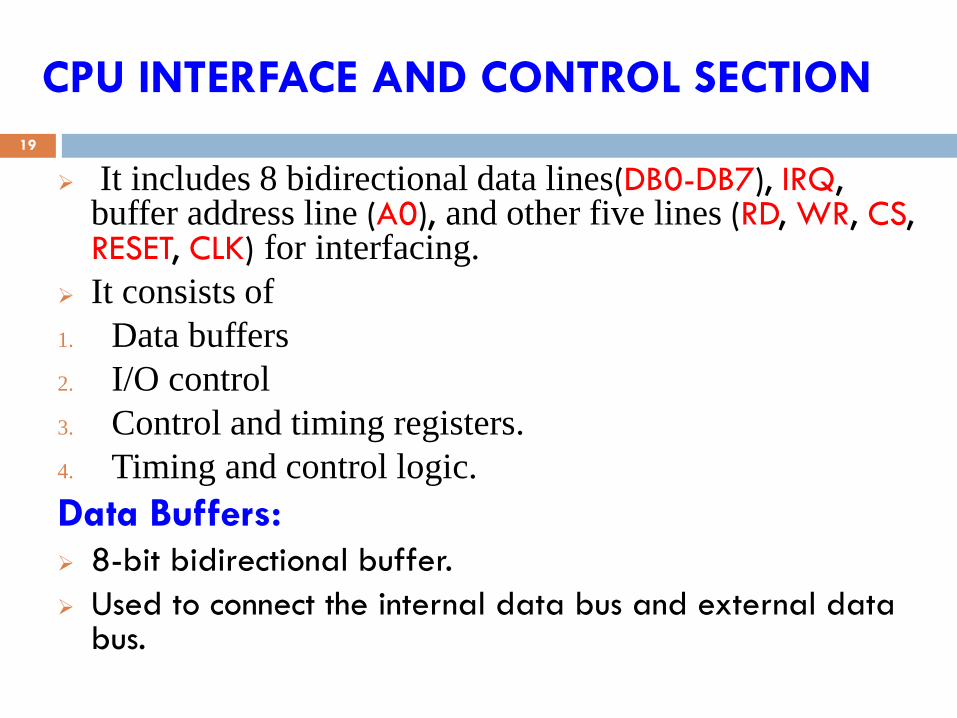
CPU INTERFACE AND CONTROL SECTION
It includes 8 bidirectional data lines(DB0-DB7), IRQ,
buffer address line (A0), and other five lines (RD, WR, CS, RESET, CLK) for interfacing.
It consists of
1. Data buffers
2. I/O control
3. Control and timing registers.
4. Timing and control logic.
Data Buffers: 8-bit bidirectional buffer.
Used to connect the internal data bus and external data bus.
19
contd.
20
contd.
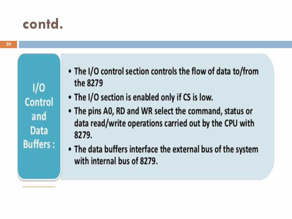
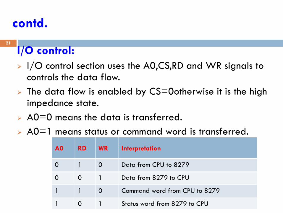
I/O control:
I/O control section uses the A0,CS,RD and WR signals to controls the data flow.
The data flow is enabled by CS=0otherwise it is the high impedance state.
A0=0 means the data is transferred.
A0=1 means status or command word is transferred.
21
A0 RD WR Interpretation
0 1 0 Data from CPU to 8279
0 0 1 Data from 8279 to CPU
1 1 0 Command word from CPU to 8279
1 0 1 Status word from 8279 to CPU

contd.
22

Scan section
The Scan Counter has two modes to scan the key matrix and refresh the display.
1. Encoded mode
2. Decoded mode.
In the Encoded mode, the counter provides a binary count that is to be externally decoded to provide the scan lines for keyboard and display. i.e. In the encoded mode, the scan counter provides a binary count from 0000 to 1111 on the four scan lines (SL3-SL0). This binary count must be externally decoded to provide 16 scan lines. Display can use all 16 scan lines to interface 16 digit 7-segment display, but keyboard can use only 8 scan lines out of 16 scan lines.
23

Scan section
In the decoded mode, the internal decoder
decodes the least significant 2 bits of binary
count and provides four possible combinations
on the scan lines (SL3-SL0).
These lines can be used directly to interface 4
digit 7-segment display, 8x4 matrix keyboard.
In general, SL3-SL0can be connected to the
rows of a matrix keyboard and the digit drivers
of a multiplexed display.
24
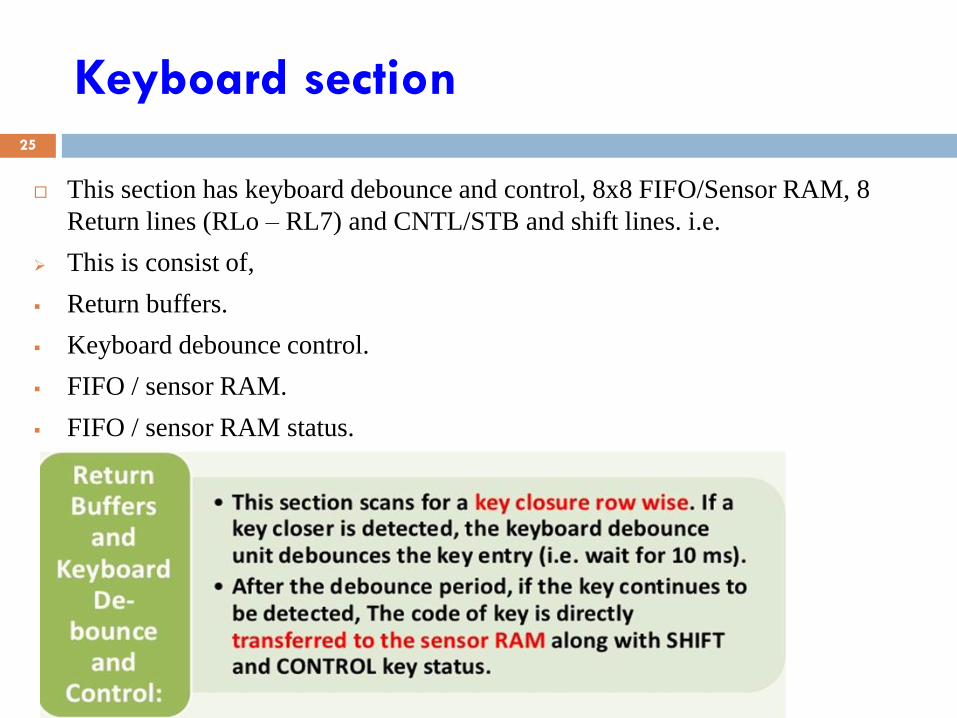
Keyboard section
This section has keyboard debounce and control, 8x8 FIFO/Sensor RAM, 8
Return lines (RLo – RL7) and CNTL/STB and shift lines. i.e.
This is consist of,
Return buffers.
Keyboard debounce control.
FIFO / sensor RAM.
FIFO / sensor RAM status.
25
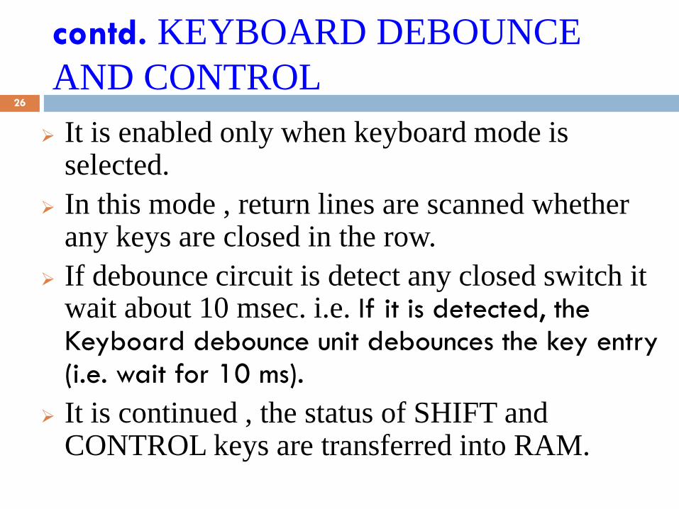
contd. KEYBOARD DEBOUNCE
AND CONTROL
It is enabled only when keyboard mode is selected.
In this mode , return lines are scanned whether any keys are closed in the row.
If debounce circuit is detect any closed switch it wait about 10 msec. i.e. If it is detected, the Keyboard debounce unit debounces the key entry (i.e. wait for 10 ms).
It is continued , the status of SHIFT and CONTROL keys are transferred into RAM.
26
contd.
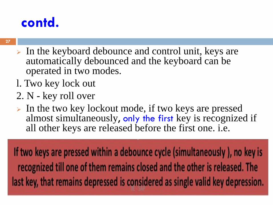
In the keyboard debounce and control unit, keys are automatically debounced and the keyboard can be operated in two modes.
l. Two key lock out
2. N - key roll over
In the two key lockout mode, if two keys are pressed almost simultaneously, only the first key is recognized if all other keys are released before the first one. i.e.
27
contd.
2. N - key roll over
In the N-key rollover mode, simultaneous keys
are recognized and these codes are stored in the
internal buffer.
28

contd.
29
contd.
FIFO/SENSOR RAM:
In Keyboard or strobed input mode, this block acts as 8-byte first-in-first-out (FIFO) RAM.
Each key code of the pressed key is entered in the order of the entry, and in the meantime, read by the CPU, till the RAM becomes empty.
The FIFO/Sensor RAM –consists of 8x8 registers that can store eight keyboard entries; each is then read in the order of entries.
30
contd.
FIFO/SENSOR RAM Status:
This is used to tell the status of FIFO/SENSOR
RAM.
The status of logic also makes IRQ signal is
High , When FIFO is empty.
The FIFO/Sensor RAM status - keeps track of
the number of entries and provides an IRQ
(interrupt request) signal when the FIFO is not
empty.
31
Display section
It consists of,
1. Display RAM.
2. Display Address registers.
3. Display registers.
DISPLAY RAM: It is a 16*8 RAM.
Which stores 16 digits display codes.
It can be accessed by CPU directly. i.e. The MPU can write into or read from any of these display RAM registers.
In Decoded mode,8279 uses only first four location of Display RAM.
In Encoded mode,8279 uses all 16 location for 16 digits display.
32

contd. Display section
DISPLAY ADDRESS REGISTERS:
Used to hold address of the byte currently write or
read by the CPU and scan count value.
In auto increment mode, address in the register is
automatically incremented for each write or read.
DISPLAY REGISTERS:
It is a Two 4-bit registers such as , A and B.
They hold the bit patterns of character to be displayed.
The content of display registers A and B can B
blanked and inhibited individually.
33
contd. Display section
The OUTA3-A0 and OUTB3-B0 output ports –
these are used for sending data to display drivers
from Display RAM and can be connected to the
segment input of 7 segment display or row inputs of dot matrix displays. The data from these outputs is
synchronized to the scan lines (SL0-SL3) for multiplexed digit display (i.e., when value on SL3-SL0 is 0000, ports will have data from register 0 of Display RAM, and so on.
The BD line is used to blank the display or the two 4-bit ports can be blanked independently.
34
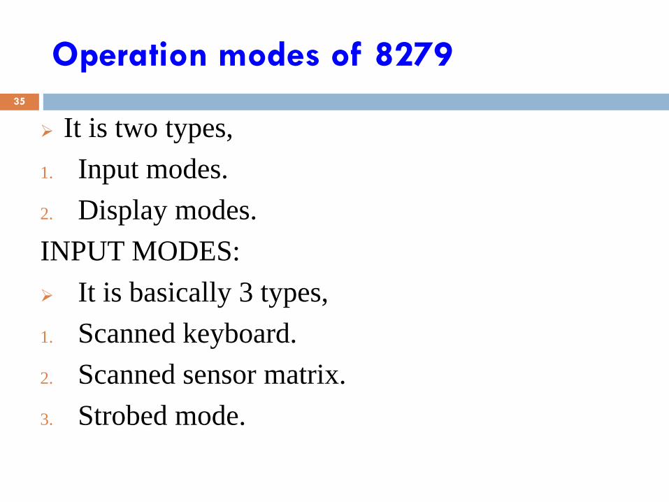
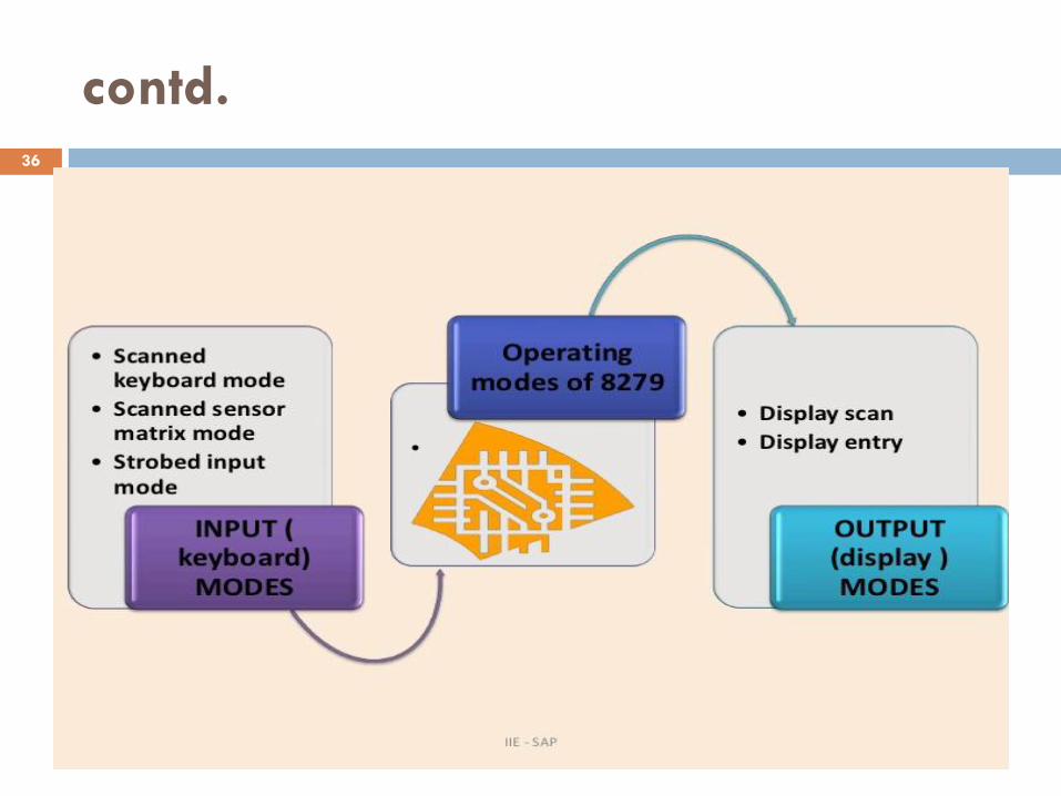
Operation modes of 8279
It is two types,
1. Input modes.
2. Display modes.
INPUT MODES:
It is basically 3 types,
1. Scanned keyboard.
2. Scanned sensor matrix.
3. Strobed mode.
35
contd.
36
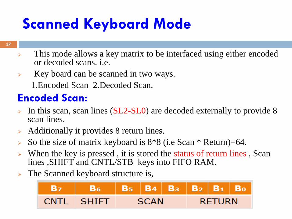
Scanned Keyboard Mode
This mode allows a key matrix to be interfaced using either encoded or decoded scans. i.e.
Key board can be scanned in two ways.
1.Encoded Scan 2.Decoded Scan.
Encoded Scan: In this scan, scan lines (SL2-SL0) are decoded externally to provide 8
scan lines.
Additionally it provides 8 return lines.
So the size of matrix keyboard is 8*8 (i.e Scan * Return)=64.
When the key is pressed , it is stored the status of return lines , Scan lines ,SHIFT and CNTL/STB keys into FIFO RAM.
The Scanned keyboard structure is,
37
contd.
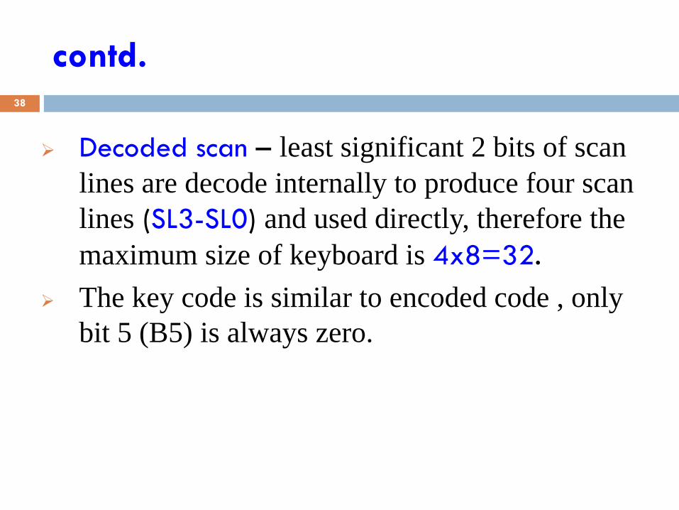
Decoded scan – least significant 2 bits of scan
lines are decode internally to produce four scan
lines (SL3-SL0) and used directly, therefore the
maximum size of keyboard is 4x8=32.
The key code is similar to encoded code , only
bit 5 (B5) is always zero.
38

contd.
39
Scanned Sensor Matrix:
In this mode, a sensor array can be interfaced
with 8279 using either encoder or decoder scans.
In this mode , image of the sensor matrix is kept in
the sensor RAM.
The status of sensor switches are input directly to
the sensor RAM.
8279 scans row one by one and store the status of
each row in the corresponding memory location.
the debounce logic is inhibited.
40

Strobed Input :
In this mode, if the control line goes low, the data
on return lines, is stored in the FIFO byte by byte.
data on return lines are transferred to FIFO on rising edge of CNTL/STB .
41

Output (Display) mode:
8279 provides two output modes for selecting
the display options.
1. Display Scan:
2. Display Entry:
Display scan: 8 or 16 character multiplexed
displays that can be organized as dual 4-bit or
single 8-bit.
Display Entry format:- Right entry or Left entry
display formats.
42

contd.
43
contd. Output (Display) mode:
Display format
Left entry
. each display position directly corresponds to a byte (or nibble) position in the display RAM.
. the 8279 displays characters from left to right in the multiplexed displays like a typewriter.
AUTOINCREMENT IN LEFT ENTRY:
In left entry mode , Auto increment flag is set after each operation display RAM address is incremented.
Right entry
.the 8279 displays characters from right to left in the multiplexed display like a calculator.
AUTOINCREMENT IN RIGHT ENTRY:
In right entry mode , Auto increment flag is set after each operation display RAM address is incremented.
44

contd.
45
Programming the 8279
The 8279 can be programmed to perform various functions through eight command words.
1. Keyboard/Display Mode Set
2. Program Clock
3. Read FIFO/Sensor RAM
4. Read Display RAM
5. Write Display RAM
6. Display Write Inhibit/Blanking
7. Clear
8. End Interrupt/Error Mode Set
All the command words or status words are written or read with A0=1 and CS=0 to or from 8279
46

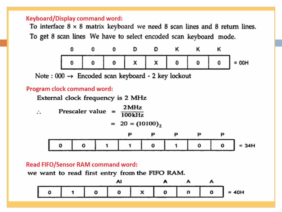
Keyboard/Display Mode Set
The format of the command word to select different modes of operation of 8279 is given below with its bit definitions.
47
Display Mode
Keyboard Mode

Program Clock
All timing and multiplexing signals for the 8279 are generated by an internal prescaler.
The clock for operation of 8279 is obtained by dividing the external clock input signal by a programmable constant called prescaler
This prescaler divides the external clock (pin 3) by a programmable integer, N.
- bits PPPPP determine the value of this integer which ranges from 2 to 31.
48
Prescaler, N= external clock
100KHz
Example
If pin 3 is clocked by 2MHz, then PPPPP is set to
10100 to divide the clock by N=20, to yield the
proper 100kHz operating frequency.
i.e. N=2MHz/100kHz=20
49

Exercise(2A)
Find the control word to operate 8279 in 100
KHz if the processor (system) clock frequency is
1 MHz.
50

Read FIFO/Sensor RAM
The CPU sets up the 8279 for a read of the FIFO/Sensor RAM by first writing this command.
In the Scan Keyboard Mode, the Auto-Increment flag (AI), and the RAM address bits (AAA) are irrelevant. The 8279 will automatically drive the data bus for each subsequent read(A0=0) in the same sequence in which the first entered the FIFO. All subsequent reads will be from the FIFO until another command is issued.
In the Sensor Matrix Mode, AAA select one of the 8 rows of the sensor RAM. If the AI flag is set (AI=1), each successive read will be from the subsequent row of the sensor RAM.(i.e. to increase the address after reading a byte from RAM.
51
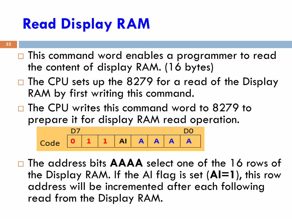
Read Display RAM
This command word enables a programmer to read the content of display RAM. (16 bytes)
The CPU sets up the 8279 for a read of the Display RAM by first writing this command.
The CPU writes this command word to 8279 to prepare it for display RAM read operation.
The address bits AAAA select one of the 16 rows of the Display RAM. If the AI flag is set (AI=1), this row address will be incremented after each following read from the Display RAM.
52
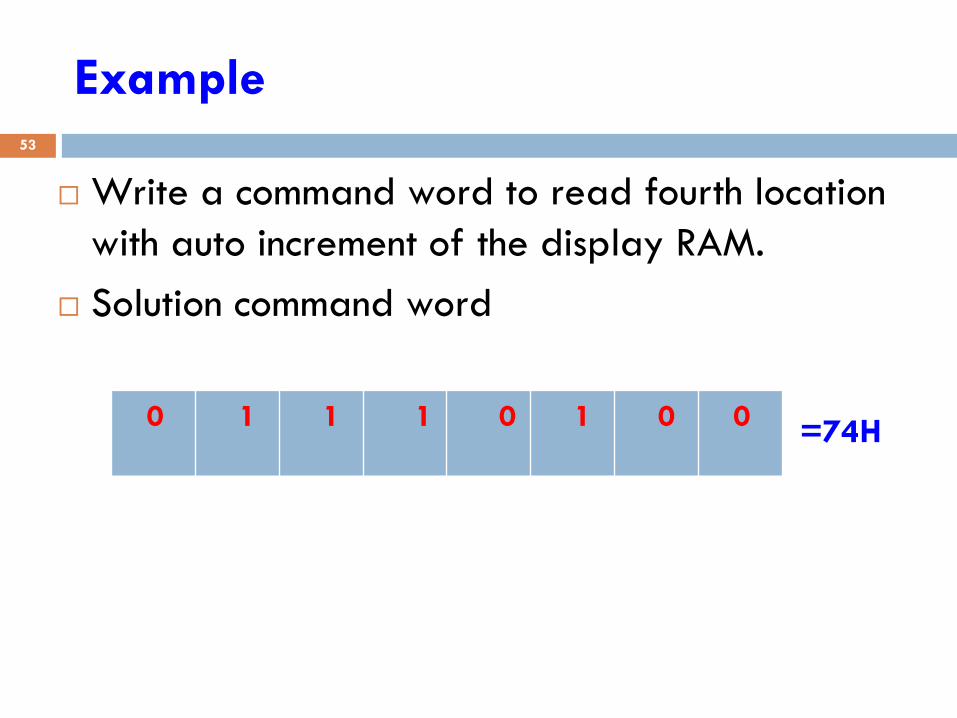
Example
Write a command word to read fourth location
with auto increment of the display RAM.
Solution command word
53
0
1 1 1 0 1 0 0
=74H

Exercise
1. Write a command word to read seventh
location with auto increment of the display
RAM.
2. Write a command word to read third location
without auto increment of the display RAM.
54

Write Display RAM
This command enables a programmer to write the display RAM data. i.e. to write data into display RAM, it is necessary to set 8279 in write display RAM mode.
The CPU sets up the 8279 for a write to the Display RAM by first writing this command.
After writing this command with A0=1, all subsequent writes with A0=0 will be to the Display RAM. If the AI flag is set (AI=1), this row address will be auto-incremented after each following write to the Display RAM.
AAAA – Selects one of the l6 rows of the Display R AM.
55
Example
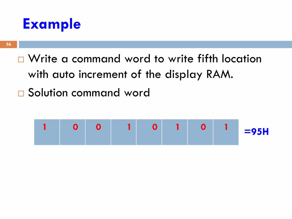
Write a command word to write fifth location
with auto increment of the display RAM.
Solution command word
56
1
0 0 1 0 1 0 1
=95H
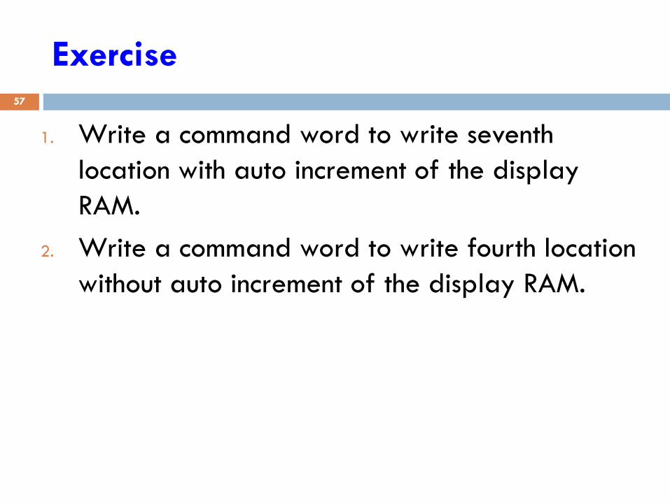
Exercise
1. Write a command word to write seventh
location with auto increment of the display
RAM.
2. Write a command word to write fourth location
without auto increment of the display RAM.
57
Display Write Inhibit/Blanking
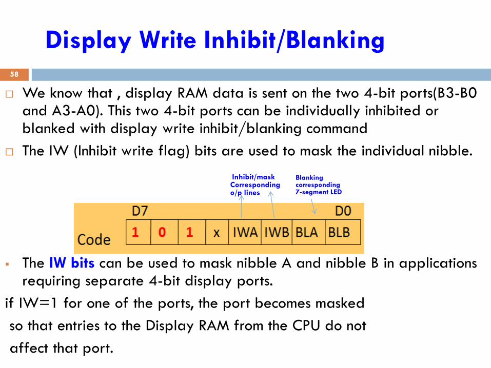
We know that , display RAM data is sent on the two 4-bit ports(B3-B0 and A3-A0). This two 4-bit ports can be individually inhibited or blanked with display write inhibit/blanking command
The IW (Inhibit write flag) bits are used to mask the individual nibble.
The IW bits can be used to mask nibble A and nibble B in applications requiring separate 4-bit display ports.
if IW=1 for one of the ports, the port becomes masked
so that entries to the Display RAM from the CPU do not
affect that port.
58
Inhibit/mask Corresponding o/p lines
Blanking corresponding 7-segment LED

contd. Display Write Inhibit/Blanking
The BL bits are used to blank each 4-bit display
ports. Both BL flags must be set to blank a
display formatted with a single 8-bit port. This
code defaults to all zeros after a reset. The Clear
command determines the code to be used as a “blank”.
Here Do and D2 corresponds to OUTBo – OUTB3
while D1 and D3 corresponds to OUTAo-OUTA3 for
blanking and masking respectively.
59

contd.
60
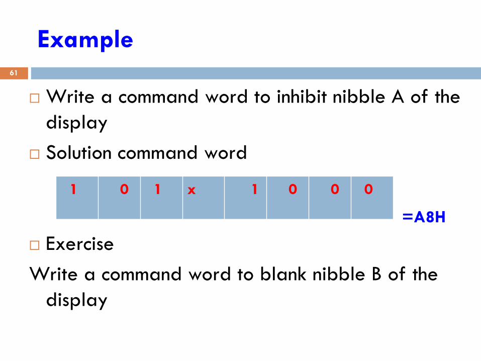
Example
Write a command word to inhibit nibble A of the
display
Solution command word
Exercise
Write a command word to blank nibble B of the
display
61
1
0 1 x 1 0 0 0
=A8H
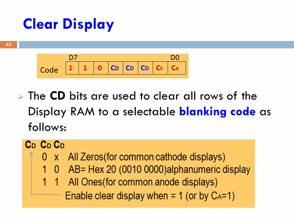
Clear Display
The CD bits are used to clear all rows of the
Display RAM to a selectable blanking code as
follows:
62

contd.
63
contd. Clear
the most significant bit of the FIFO status word is set during clearing the Display RAM.
- If CF=1, the FIFO status is cleared and the interrupt output line is reset. Also, the Sensor RAM pointer is set to row 0.
- CA (clear all bits) flag, has the combined effect of CD and CF; it uses the selected CD clearing on the Display RAM, and also clears FIFO status.
64
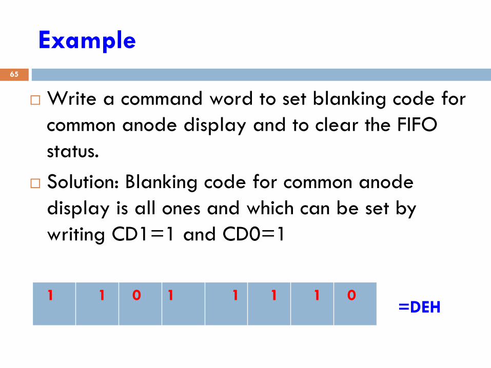
Example
Write a command word to set blanking code for
common anode display and to clear the FIFO
status.
Solution: Blanking code for common anode
display is all ones and which can be set by
writing CD1=1 and CD0=1
65
1
1 0 1 1 1 1 0
=DEH

End Interrupt/Error Mode Set
For sensor matrix mode(IRQ is used to read the key pressed).
For the sensor matrix mode, this command lowers the IRQ line and enables further writing into the RAM. Otherwise, if a charge in sensor value is detected, IRQ goes high that inhibits writing in the sensor RAM.
For the N-key rollover mode- if E=1, the chip will operate in the Scanned keyboard special Error mode.
In the special error mode, if two keys are depressed during single debounce, the error flag in the FIFO status word is set.
66

Status word :- it is used in the keyboard and strobed input modes. It contains the
FIFO status, error, and display unavailable signals.
- Overrun error occurs when the entry of another character into a full FIFO is attempted.
- Underrun error occurs when the CPU tries to read an empty FIFO.
- DU - During clear display or clear all command, display RAM is not available for user.
- S/E - in the sensor matrix a S/E bit is set to indicate that at least one sensor
closure indication is contained in the sensor RAM.
- in the scanned keyboard special error mode, a S/E bit is set to indicate that
a simultaneous multiple closure error has occurred.
Data format in FIFO
68

Example:
Find the key code for given condition below:
CNTL/STB SHIFT keys are open.
The pressed keys are to scan lines 2 and return lines 4.
SOLUTION:
B7 B6 B5 B4 B3 B2 B1 B0
1 1 0 1 0 1 0 0
CNTL=1
SHIFT=1
Scan mode=010 (Scan line 2)
Return mode=100 (Return line 4)
Key code =D4 H

. System Design
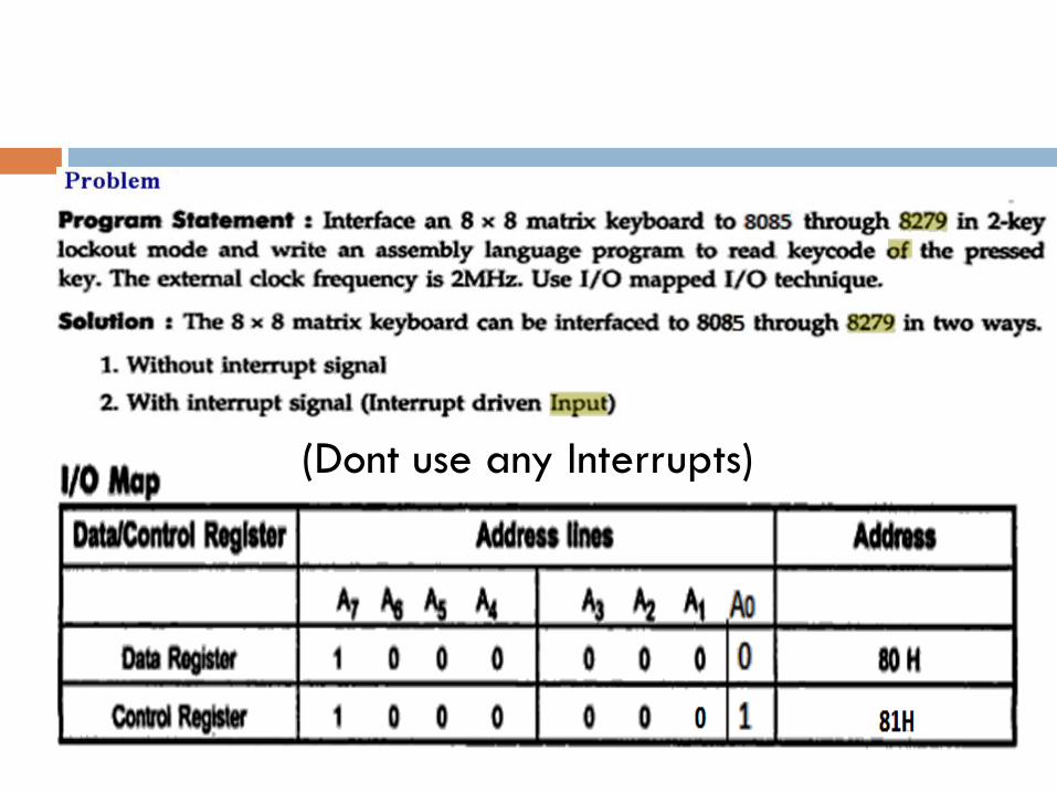
(Dont use any Interrupts)
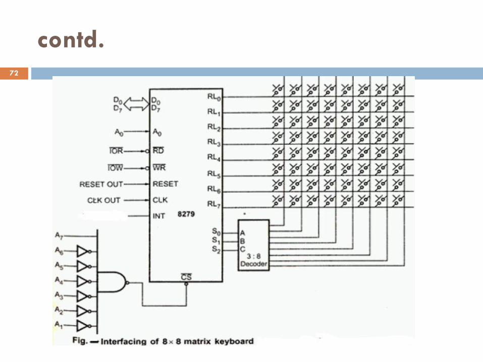
contd.
72
.
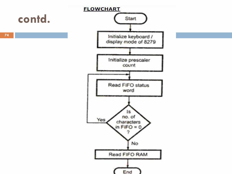
contd.
74

Source program:
MVI A, 00H : Initialize keyboard/display
OUT 81H : in encoded scan keyboard-2 keylockout mode
MVI A, 34H
OUT 81H : Initialize prescaler count
BACK: IN 81H : Read FIFO status word
ANI 07H : Mask bit B3 to B7
JZ BACK : If 0, key is not pressed wait for key press else read FIFO RAM
MVI A, 40H : Initialize 8279 in read
OUT 81H : FI FO RAM mode
IN 80H : Read FIFO RAM (keycode)
HLT : Stop program execution.
75
Exercise
76
.

.

.

LOOK UP TABLE

contd.
81


![D5200 Programmer - AlarmHow.net Programmer/D5200...D5200 Programmer FEATURES w4-Line Liquid Crystal Display wCustom Keyboard [Load, Copy, Navigate] wUp to 8 programmable passwords](https://static.fdocuments.in/doc/165x107/5aaf114b7f8b9a190d8ce28c/d5200-programmer-programmerd5200d5200-programmer-features-w4-line-liquid-crystal.jpg)

![The Keyboard and Display - UMass Amherst Keyboard and... · The Keyboard and Display [Info] number does not exist, the cursor goes to the highest ramp number in the control table.](https://static.fdocuments.in/doc/165x107/5ec929249c0da574066a2ac1/the-keyboard-and-display-umass-keyboard-and-the-keyboard-and-display-info.jpg)