The Physics of Single Event Burnout (SEB) · The Simulation Standard Page 2 July, August, September...
18
Volume 24, Number 3, July, August, September 2014 Engineered Excellence A Journal for Process and Device Engineers Introduction Single Event Burnout in a diode, requires a specific set of circumstances to occur, since there is no intrinsic cur- rent gain in the device itself to amplify the currents cre- ated by the charge from a single event strike. What has to happen for Single Event Burnout (SEB) to occur in a device with no intrinsic gain, for realistic levels of Linear Energy Transfer (LET), for any given bias is fundamen- tally simple: The total charge created by the SEU strike itself, plus any additional charge from avalanche multiplication, has to sustain a minimum current for a minimum time, to create sufficient localized self heating, that the I-V curve of the diode centered around the strike point, is modified suffi- ciently, such that the current becomes locally self sustain- ing. This self sustaining current will eventually spread throughout the device, since higher mobilities exist in the surrounding cooler parts, creating an ever expand- ing preferential current path, until irreversible damage through melting or cracking of the device occurs. If the localized self heating is insufficient to modify the I-V characteristics into a secondary stable high conduc- tion regime before the charge pulse dissipates, the device will recover from the ionizing single event strike. In this article we will attempt to provide evidence for this postulation with a methodical approach to this subject, using a high voltage PiN diode as an example. Theory It is unlikely that an SEU strike of any realistic Linear Energy Transfer (LET) is going to deposit a sufficient concentration of energy, that the SEU strike alone will immediately create irreversible damage from melting or thermally expansive cracking. If this were the case, power diodes would experience periodic permanent fail- ure, without any applied bias. In other words, previously working diodes could fail, even if they were simply be- ing stored as individual components, without even being connected to any circuit. The author is not aware of any proven cases of such phenomenon. If we accept that the deposited energy from the SEU strike alone cannot create Single Event Burnout (SEB) phenom- enon, then we must accept that additional energy from the applied bias in the circuit surrounding the diode is responsible for providing the destructive energy. This statement suggests that circuit and component design criteria can therefore play a role in the probability of an SEB event occurring in a circuit. At this point the postulation needs to be re-stated that a current of sufficient magnitude is required to eventu- ally heat the device to destruction, and that this current must be present for a sufficient length of time for the criti- cal temperature rise to occur before the device recovers. What limits the rate of temperature increase with time is the specific heat capacity of the substrate material (sili- con in this case study) and heat removal from thermal conduction to cooler parts of the device. These consider- ations strongly suggest, therefore, that in order for SEB to occur, the effected device must be transferred to a sec- ondary stable state in the IV characteristics, so that regen- erative feedback can occur, to continue supplying high power in that stable state, eventually causing irreversible thermally induced damage. INSIDE Multiple SEU Strike Simulations on a Six Transistor 20nm SRAM Cell ................................. 7 Single Event Gate Rupture (SEGR) Simulations in Vertical Planar Power MOSFETs ..................... 9 Hints, Tips and Solutions ......................................... 13 Continued on page 2 ... The Physics of Single Event Burnout (SEB)
Transcript of The Physics of Single Event Burnout (SEB) · The Simulation Standard Page 2 July, August, September...
July, August, September 2014 Page 1 The Simulation StandardVolume 24, Number 3, July, August, September 2014
Engineered Excellence A Journal for Process and Device Engineers
IntroductionSingle Event Burnout in a diode, requires a specific set of circumstances to occur, since there is no intrinsic cur-rent gain in the device itself to amplify the currents cre-ated by the charge from a single event strike. What has to happen for Single Event Burnout (SEB) to occur in a device with no intrinsic gain, for realistic levels of Linear Energy Transfer (LET), for any given bias is fundamen-tally simple:
The total charge created by the SEU strike itself, plus any additional charge from avalanche multiplication, has to sustain a minimum current for a minimum time, to create sufficient localized self heating, that the I-V curve of the diode centered around the strike point, is modified suffi-ciently, such that the current becomes locally self sustain-ing. This self sustaining current will eventually spread throughout the device, since higher mobilities exist in the surrounding cooler parts, creating an ever expand-ing preferential current path, until irreversible damage through melting or cracking of the device occurs.
If the localized self heating is insufficient to modify the I-V characteristics into a secondary stable high conduc-tion regime before the charge pulse dissipates, the device will recover from the ionizing single event strike.
In this article we will attempt to provide evidence for this postulation with a methodical approach to this subject, using a high voltage PiN diode as an example.
TheoryIt is unlikely that an SEU strike of any realistic Linear Energy Transfer (LET) is going to deposit a sufficient concentration of energy, that the SEU strike alone will immediately create irreversible damage from melting or thermally expansive cracking. If this were the case, power diodes would experience periodic permanent fail-ure, without any applied bias. In other words, previously working diodes could fail, even if they were simply be-
ing stored as individual components, without even being connected to any circuit. The author is not aware of any proven cases of such phenomenon.
If we accept that the deposited energy from the SEU strike alone cannot create Single Event Burnout (SEB) phenom-enon, then we must accept that additional energy from the applied bias in the circuit surrounding the diode is responsible for providing the destructive energy. This statement suggests that circuit and component design criteria can therefore play a role in the probability of an SEB event occurring in a circuit.
At this point the postulation needs to be re-stated that a current of sufficient magnitude is required to eventu-ally heat the device to destruction, and that this current must be present for a sufficient length of time for the criti-cal temperature rise to occur before the device recovers. What limits the rate of temperature increase with time is the specific heat capacity of the substrate material (sili-con in this case study) and heat removal from thermal conduction to cooler parts of the device. These consider-ations strongly suggest, therefore, that in order for SEB to occur, the effected device must be transferred to a sec-ondary stable state in the IV characteristics, so that regen-erative feedback can occur, to continue supplying high power in that stable state, eventually causing irreversible thermally induced damage.
INSIDEMultiple SEU Strike Simulations on a Six Transistor 20nm SRAM Cell ................................. 7Single Event Gate Rupture (SEGR) Simulations in Vertical Planar Power MOSFETs ..................... 9Hints, Tips and Solutions ......................................... 13
Continued on page 2 ...
The Physics of Single Event Burnout (SEB)

The Simulation Standard Page 2 July, August, September 2014
In simple terms, the postulation above, requires that the IV curve of the structure has a “snapback” type of characteristic, such that for some of the possible range of applied bias voltage, there will be at least two possible current densities that are stable. One a low current den-sity “off” state, and one self sustaining “on” state, where the current density is sufficient to melt the device after a certain time. If this “snapback” condition in the device IV characteristics is met, then the SEU strike simply acts as a trigger to transfer the IV characteristics from a stable cold “off” state, to a new hotter and also stable “on” state.
Despite the fact that “snapback” characteristics are usu-ally only associated with devices that have intrinsic gain, we will show that “snapback” characteristics also occur in PiN diodes, and is especially severe when self heating effects are taken into account. We will attempt to show in this article, that It is these temperature dependent IV characteristics that are the root cause of Single Event Burnout (SEB) in high power PiN diodes. These simula-tions will also demonstrate a new and simple methodol-ogy to assess the approximate sensitivity of other devices to SEB, using a simple D.C. I-V simulation. Testing the applicability of this new method to other diode device types, however, will be left as future work.
D.C. SimulationsIn this article, examples of power PiN diodes described in a paper by A.M. Albadri et. al., [1] will be used to demon-strate the simulation of Single Event Burnout. These PiN power were designed for a maximum operating voltage of 3,500V. The diodes were essentially one dimensional in nature, so simulation of the 3D effects using circular sym-metry with a central SEU strike location was sufficient. The diodes had an intrinsic drift region 400um thick with an unintentionally doped n-type concentration of 3.1e13/cm3, as described in reference [1]. The only difference in
the simulations described here, is that in the interests of simulation speed and other reasons described later in this article, the radius of the diode in the simulation space was only 5um rather than the full 400um of the real device.
From the arguments put forward as to the root cause of SEU being a stable “snapback” characteristic, the first step is to simulate the full I-V characteristics of the di-ode. Figure 1 shows the full I-V characteristic of the PiN power diode at a constant temperature of 300K.
The I-V curve shown in Figure 1 immediately shows us important information as regards the sensitivity of this device to a “fast” SEU event. By a “fast” SEU event, it is meant, “an event providing a sufficient level of current injection after avalanche multiplication is taken into ac-count, that the device transfers to a self sustaining high current state without even considering any significant self heating effects”.
From Figure 1, it can be deduced that this diode is not susceptible to such as event for any reverse bias less than 2,400 volts, because a secondary and stable high current condition simply does not exist below 2,400 volts. How-ever the currents required directly from the SEU strike in order to transfer the diode to it’s high current “on” state are in the range of Amps, making this an unlikely event. From this I-V curve, we can immediately deduce that a Single Event Burnout (SEB) is very unlikely without self heating effects transforming the secondary stable high current state towards a lower current density.
The curve from Figure 1 shows that if the diode was bi-ased at 3500 volts, a current of approximately 5 amps would be required to initiate a stable self sustaining “on” state. Extrapolating from SEU current curves versus LET energy discussed later in this article, this would require a strike with an LET value of over a thousand MeV.cm2/mg which is not a likely event.
Figure 1. Constant temperature (300K) I-V curves of the 3,500 volt power PiN power diode.
Figure 2. Comparing the no self heating, with a thermal equilib-rium curve.

July, August, September 2014 Page 3 The Simulation Standard
The usefulness of this constant temperature I-V curve, is that it defines one of the two operating boundary condi-tions. In this case, the boundary condition being where no self heating occurs.
Now let us define the other boundary condition, where the current from an SEU strike continues for sufficient time, such that localized “thermal equilibrium” occurs. Figure 2 shows the original constant temperature curve of Figure 1, but this time over-lays the I-V curve simulated with the localized self heating model activated. Since this is a DC bias sweep, then at each point of the I-V curve, thermal equilibrium has been established.
Figure 2 immediately shows how vulnerable a power PiN diode could be, when the effects of self heating are taken into account. Now a sustained current of only tens of micro Amps is required at higher reverse bias voltage, in order for a self sustaining, thermal runaway event to occur. The required current for thermal runaway rapidly increases at lower bias voltages giving rise to the expected behavior that an SEB event is more likely at high reverse bias voltages, or saying the same thing in another way, an
SEU with a higher value of LET is required at lower bias voltages in order to trigger an SEB event.
Figure 3 shows the temperature at two significant regions in the device, the red curve showing the metallurgic junc-tion temperature and green curve at the intrinsic to N+ boundary. It should be noted that the heat sink was de-fined as coinciding with the anode contact, which is the closet to the metallurgic junction, which is why metallur-gic boundary curve has a lower temperature.
Since in a transient SEU strike, thermal equilibrium is not usually obtained, we now know our realistic I-V curve will trace a path somewhere between these two extremes. The most useful predictor of device behavior is therefore to emulate I-V curves that show a more realistic current temperature curve, between the two extremes shown in Figure 2, to approximate the IV curve followed by an SEU current pulse being far from thermal equilibrium.
In the author’s opinion, the most relevant way to plot these intermediate I-V curves is to artificially increase the thermal conductivity of the substrate material. This re-sults in a temperature rise with conduction current that does not occur if the method of using different constant temperature simulations are used, as in the case for some of the simulations shown in reference [1]. Another meth-od to produce a non equilibrium I-V curve would be to use a voltage time transient simulation, but this method suffers from the complication that another variable has to be accounted for, namely the avalanche multiplication time, which can result in serious voltage overshoot as the avalanche multiplication process builds up. The voltage overshoot also depends on the chosen ramp rate.
Using this new method of increasing the thermal conduc-tivity to emulate transient, heating effects, a number of simulations were run multiplying the thermal conductiv-ity by x10, x100, x1,000, x10,000 and x100,000. These ad-ditional curves are added to the original curves shown in Figure 2 and are now plotted in Figure 4.
Figure 3. Temperatures inside the PiN diode at the metallurgic junction and at the N+ to intrinsic boundary.
Figure 4. I-V curves using increasing thermal conductivity to em-ulate non thermal equilibrium effects from an SEU strike.
Figure 5. Showing the relationship between LET required (induced current) to induce an SEB event and applied reverse bias.

The Simulation Standard Page 4 July, August, September 2014
From Figure 4, several effects are apparent. From the origi-nal constant 300K temperature (red) curve, it seemed that Single Event Burnout (SEB) could not occur for reverse applied voltages of less than approximately 2,400 volts. However, as can be seen from Figure 4, the longer the SEU transient current lasts and therefore the hotter the local temperature gets, the lower this critical reverse ap-plied voltage becomes where SEB can occur. In addition, to a lower critical voltage, the hotter the local tempera-ture becomes, the lower the current required before the secondary high current stable “on” condition is reached. It will be shown later, that the yellow curve, representing the thermal conductivity increased by 10,000 times, is a reasonable approximation to the real transitory curves. Further simulations showed that the appropriate value of thermal conductivity multiplier for this particular PiN diode was between, 4,500 and 5,000.
Figure 5 shows D.C. simulations using a thermal conduc-tivity 4,500 times the equilibrium value, with cathode cur-rent plotted on a linear scale between zero to 0.25 Amps, versus reverse applied voltage. It will be shown later, that the cathode current range between zero and 0.25 Amps represents the same range of currents induced by the Single Event Upset in this study, with a Linear En-ergy Transfer values of up to 128 MeV.cm2/mg. On this curve, by converting the cathode current on the vertical axis to equivalent LET value, you can directly read off the LET required to trigger a single event burnout event for any given reverse bias on the PiN diode. Clearly, the reverse bias cannot exceed the 3,500 volt breakdown voltage, so bias voltages shown in Figure 5 above 3,500 volts are not meaningful. In this curve, the initial break-down currents at 3,500 volts are simply disguised by the linear scale on the Y axis.
This conversion between LET value and induced cur-rent in the diode is plotted in Figure 6. It should be noted that in order for a similar thermal conductivity multiplier value to apply to other devices, there is a gen-eral requirement that before the onset of the destructive SEB event, the temperature laterally across the device width (ie the X direction in this case) is approximately uniform within a fraction of a micro second or so, which results in the general requirement that the width of the simulated section of the device be in the order of a few microns. If this new concept is to be applied to a very wide device, then the concept of localized current den-sity in the region of the SEU strike should be applied rather than simply total current. This requirement is a secondary reason for the simulation width of the device being only 5 um.
Figure 6. Conversion between Induced Cathode Current in Figure 5 and LET Value.
Figure 7. Temperature and Current Simulations of SEU strikes with LET values from 4 to 128 MeV.cm2/mg at a reverse bias of 2,700 volts.

July, August, September 2014 Page 5 The Simulation Standard
Transient SimulationsTransient simulations of a Single Event Upset (SEU), for various levels of Linear Energy Transfer (LET) were in-vestigated for two reverse bias points for the PiN diode, namely 2,700 and 3,500 volts. The first bias was chosen based on the results from reference [1], where it was shown that Single Event Burnout (SEB) in this particular diode was unlikely for a reverse bias of much less than 2,700 volts, and the second bias of 3,500 volts was chosen since it was close to the maximum operating voltage of the diode, so a lower value of LET would be expected to trigger Single Event Burnout (SEB).
The characteristics of the SEU pulse were chosen to match those in reference [1], meaning that the centroid of the pulse occurred at a simulation time of 5 pico seconds and the width of the pulse was 0.2 pico seconds with an effec-tive radius of 20 nano meters.
The LET of the first SEU pulse transient simulation was 4 Mev.cm2/mg, and this LET value was then subsequently doubled and re-simulated in an automated loop until an
irreversible SEB event occurred. The results of the tran-sient simulations for the two reverse bias points of 2,700 volts and 3,500 volts are shown in Figures 7 and 8 respec-tively. Also shown are simulations at a fixed temperature of 300K in Figure 9, showing that no SEB event occurred as predicted by the I-V curve shown in Figure 1, where as previously discussed, an LET value of over a 1,000 would be required for an SEB event to occur.
It can be observed from Figures 7, 8 and 9, that transient simulations of SEU strikes with any realistic LET value, result in an initial induced current pulse that is approxi-mately constant over many orders of magnitude of time, and further is almost proportional to the LET value of the SEU strike. This is how the simple conversion from LET value to cathode current can be calibrated and is the source of the data shown in Figure 6. It is this flat portion of the current with time translates to the current in the DC I-V curves in Figures 4 and 5.
Form the transient simulations we can deduce that for an SEB event to occur at a bias of 2,700 volts, an SEU strike with an LET value between 64 and 128 MeV.cm2/mg is required, whilst at a bias of 3,500 volts, an SEU strike with an LET value of between 16 and 32 MeV.cm2/mg is needed. Using the conversion shown in Figure 6, a bias of 2,700 volts equates to a required current of between 0.12 and 0.24 Amps for an SEB event and a bias of 3,500 volts equates to a required current of between 0.029 and 0.06 Amps to trigger and SEB event.
Placing these error bars on to Figure 5, we can see that our approximately calibrated DC simulations with a thermal conductivity multiplier of 4,500 results in an IV curve which just about predicts these results to within these error bars, validating this technique as a reasonable approximation for a first pass predictive tool for silicon based devices. Clearly, further calibration would be ex-pected for other materials due to significantly differing thermal properties.Figure 9. The same simulations as Figure 8, but without localized
lattice heating and a substrate temperature of 300K.
Figure 8. The same simulations as in Figure 7, but with a reverse bias of 3,500 volts.

The Simulation Standard Page 6 July, August, September 2014
ConclusionsIt has been shown in this article that the fundamental cause of single event burnout, results from the existence of two stable currents in the I-V curve of the device. An SEB event occurs when an ionizing strike allows the tran-sition between a stable low current bias point on the I-V curve to an alternative stable high current bias point on the I-V curve. Whilst the high current conducting state is a moving target during the transitory strike because of temperature effects, it appears that the mechanics of single event burnout are simple in essence.
A novel concept in this article was also introduced, in which the results from a series of transient, non thermal equilibrium SEB simulations can be predicted reason-ably well from a single DC thermal equilibrium I-V curve simulation, by modification of the thermal conductivity, to emulate the real non thermal equilibrium event. This simple modification to the DC simulation approximately captures the “moving target” of the I-V curve caused by the transitory non equilibrium temperature rise of the de-vice during the SEU strike.
The single value of thermal conductivity required for the predictive DC simulation has been approximately cali-brated in this work and the multiplying factor was found to be about 4,500 to 5,000 times the thermal equilibrium conductivity value. Further work is required to find out how universally applicable this approximately calibrated value is to other diode types and designs. In any event, the multiplier approximately calibrated in this work can be a reasonable first guess for other device types.
References[1] “Coupled Electro-Thermal Simulations of Single Event
Burnout in Power Diodes”, IEEE Transactions on Nuclear Science, Vol. 52, No. 6, December 2005.

July, August, September 2014 Page 7 The Simulation Standard
Multiple SEU Strike Simulations on a Six Transistor 20nm SRAM Cell
Figure 1. Basic lower layers of the SRAM designed using MaskViews.
Figure 2. Full 3D process simulated structure of the six transis-tor 22nm SRAM cell, including interconnect, showing absolute net doping.
Table 1. Truth table for flip flop states after an SEU strike.
Previous State MOS 1 Strike MOS 2 Strike
nMOS 1 OFF ON ON ON OFF OFF
nMOS 2 ON OFF OFF OFF ON ON
IntroductionIt is often not realized that more than one Single Event Up-set (SEU) statement can be used in a simulation. Each SEU statement can locate a strike anywhere in the semiconductor and at any time during the transient, offering a range of sim-ulation possibilities. One possible use for simulating mul-tiple SEU strikes is for simulating spallation events, where a high energy particle, such as a cosmic ray, suffers a nuclear interaction, producing one or more different sources of ion-izing particle at the nuclear reaction site. In this article, we will, demonstrate two SEU strikes in different locations at two different times on a full six transistor 22nm SRAM cell, including four layers of metal interconnect.
Simulation Set UpA standard six transistor SRAM cell layout was created in MaskViews, with the major lower layers shown in Fig-ure 1. As can be seen from Figure 1, the entire SRAM cell measures only 0.35um x 0.2um. Next a 22nm process flow was developed for both nMOS and pMOS transis-tors and simulated using Victory Process (Cell Mode). Monte-Carlo implantation was used throughout in the interests of creating realistic doping profiles, typically simulating 40 million ions per implant.
The full 3D process simulated SRAM cell, including all relevant interconnect, is shown in Figure 2 with the insu-lating layers removed for clarity. The design of the lay-out and process flow allowed satisfactory operation at a power supply line voltage of just 0.8 volts.
The first task when simulating a cell’s sensitivity to a single event upset (SEU) event is to locate sensitive areas of the circuit that will be especially sensitive to a transis-tor transitioning from an off state to an on state, since an SEU strike effectively forces a transistor into a conduct-ing state, whether it was previously conducting or not. It is also intuitively clear that since an SRAM circuit is geo-metrically symmetrical, it is not possible in advance to
predict the SRAM cell’s logical output state on power-up. Thus which of the individual transistors in the SRAM cell are in the off state and are therefore most sensitive to an SEU strike, is also not known in advance.
To solve the issue of not knowing which transistors are conducting on power up and which are not, two SEU strikes were applied with a staggered time interval in be-tween the two strikes. Each nMOS transistor in the active flip flop, were struck in the central channel region in turn, with the staggered time interval between strikes being long enough, such that a circuit recovery or a logic state flip, would be established before the next strike occurred. With this sequence, at least one logic flipped state could be guaranteed, as shown in the truth table below, which represents an SEU powerful enough to always flip the state of the flip flop, if it hits the channel of the off state transistor. Remember, if the truth table initially looks confusing, that if the off state transistor is flipped, then the other previously on transistor will be forced to it’s off state, such that transistors nMOS1 and nMOS2 in the flip flop truth table are always eventually forced into op-posite states.
Following the truth table, we can see that the flip flop will either change state once or twice depending on whether the first strike hits a transistor in the off state or the on state.

The Simulation Standard Page 8 July, August, September 2014
Figure 3. Power on Output Characteristics of the SRAM Cell. Figure 5. SRAM Output when the First Strike Occurs on the “Off” state nMOS.
Figure 6. SRAM Output when the First Strike Occurs on the “On” state nMOS.
Figure 4. Schematic Showing Location of the Two SEU Strikes at M1 and M3.
Simulation ResultsThe entire simulation sequence was run in transient mode, including the initial ramp up of the power sup-ply. The power supply was ramped up to 0.8 volts in 1 nano second, and then left to stabilize for a further 1 nano second. This ramp up sequence provided the plot of supply voltage versus the SRAM output states Q and Q_bar, as shown in Figure 3. The output states of Q and Q_bar started to separate to their opposite states at ap-proximately half the supply voltage, showing that a sup-ply voltage of 0.8 volts provided ample positive feedback for the flip flop to work adequately.
The second part of the transient, simulated the two SEU strikes, 2 nano seconds apart. Two nano seconds proved to be sufficient time for the SRAM to either recover or suf-fer an output state flip, depending on whether the SEU strike hit a transistor in the “on” state or in the “off” state respectively.
The SEU strikes were defined with a radius of 25 nano meters and a pulse width of 1 pico second and were lo-cated in the channel region of the transistors “M1” and “M3” in the schematic diagram shown in Figure 4. Fig-ure 5 shows what happens when the “off” state nMOS gets struck first. In this case, the struck transistor mo-
mentarily conducts more than it’s complementary pMOS, pulling down the output voltage at that node, which flips the memory state of the SRAM. This results in the other nMOS transistor, that was previously in the “on” state, being transferred into the “off” state. Now when this transistor, now in an off state, is hit with the secondary SEU strike, the SRAM cell output flips once again.
Figure 6 shows what happens if the transistor that gets struck first was in a conducting (“on”) state. Since the transistor was already conducting, making it conduct even more, has little effect on the output of the SRAM cell, except for a voltage transient which momentarily pulls down the output, from which it quickly recovers. Since the SRAM did not change state, the other nMOS must be in the “off” state, so when this transistor gets hit with the second SEU strike, the SRAM cell flips state as expected.
ConclusionsWe have demonstrated dual Single Event Upset (SEU) strikes at different locations and at different times on a 22nm six transistor SRAM cell structure created in Vic-tory Process (Cell Mode), and using the Victory Device Simulator for the transient device simulations.

July, August, September 2014 Page 9 The Simulation Standard
Single Event Gate Rupture (SEGR) Simulations in Vertical Planar Power MOSFETs
IntroductionPower MOSFETs exposed to particle-rich, space-like or terrestrial, environment, can exhibit Single Event Gate Rupture (SEGR) and Single Event Burnout (SEB). The use of power devices as high power solid state switches for the electric and hybrid car manufacturers, has generated new non-military, and non-space interest power device failure modes. A SEGR event is one such failure mode and the simulation of such an event is the subject of this article.
An irradiation event by a high-energy particle interact-ing with the material of a device gradually loses energy as it passes through the device, transferring its energy to the material by ionizing events. The net result is a high-density ionized track.
If the area of the device, through which the ionizing par-ticle passes, has no internal electric field, then to a large extent, the high density of positive (hole) and negative (electron) charges created by the track, simply recom-bine, with the absence of an electric field to separate these charges by any meaningful distance.
Given there is an electrical field in the device prior to the strike, the high density of electron and hole pairs created by the primary particle can become separated. Once the positive and negative charges, escaping recombination, have become separated, the electrical field in the device is disturbed to a degree dependent on the Linear Energy Transfer (LET in MeV-cm2/mg) of the ionizing particle and the bias conditions of the device.
In a Single Event Gate Rupture (SEGR) event, there are three generally accepted response mechanisms, the gate (often referred to as capacitor or dielectric), the epitaxial, and the substrate. The initial measure drain and gate leakage currents depend upon device characteristics and oxide quality. Such that any measurable gate current in-crease above leakage during irradiation may indicate a SEGR event has occurred.
The gate SEGR response is measured by biasing the drain at zero volts (0V), and stepping the gate voltage in in-crements until SEGR occurs for the selected ion species. The SEGR gate voltage is defined as the average voltage at which the power device exhibited SEGR and the volt-age of the previous irradiation, an irradiation data point where the power device exhibited no failures with failure being defined as gate current exceeding 1uA.
The gate component of SEGR can also be described as lowering of the intrinsic dielectric breakdown voltage
to a new value called VCRIT. This VCRIT value for silicon-dioxide (SiO2) dielectric is defined by the Titus-Wheatley equation (1) [1] below:
VCRIT = [(EBD)*(TOX)] / (1 + (Z/44)) (1)
The value VCRIT is in volts, EBD is the intrinsic dielectric breakdown field in volts per centimeter, TOX is the di-electric thickness in centimeters, and Z is the ion atomic number. The Titus-Wheatley equation is limited to ions strikes that are perpendicular to the dielectric material, as these experimental evidence supports that the lowest values of VCRIT occur for perpendicular ion strikes.[2,3]
The second response mechanism, the epitaxial response, is a distortion of the depletion field around the localized track area, which couples a portion of the drain voltage to the interface of the epitaxial layer and dielectric. This coupled voltage, VCOUPLED, induces an electric field across the dielectric and is additive to the existing electric field due to the gate voltage, VGS. The epitaxial layer provides a standoff for a high electric field within the device. In vertical power structures, the blocking voltage capabil-ity is determined by the thickness and doping of the epi-taxial layer. As thickness increases and is more lightly doped, the epitaxial blocking voltage increases, but a cost of increased on-state resistance. This makes the epitaxial response very sensitive to process and design parameters of the Power MOSFET.
The third response, the substrate response has been ex-perimentally shown to have minimal effects, even with different substrate resistivity and thicknesses [4,5] since there is no depletion layer inside the substrate.
Modeling and Simulation of Single Event Gate Rupture event in Technology Computer Aided Design (TCAD) tools, is supported by the ability to monitor gate, drain and source currents is to monitor the gate oxide field dur-ing the irradiation event.
SimulationsThe simulation methodology in this example was to reduce what would normally be a three dimensional problem into a faster two dimensional problem by using circular symmetry in the device simulations, and also to define the irradiation strike to occur vertically at the cen-ter of the circular symmetry, so as not to incur any errors in the effective charge track shape.

The Simulation Standard Page 10 July, August, September 2014
Figure 1. The device used in this SEGR case study, showing the net doping and metallurgic junctions.
Figure 2. Shows the time evolution of the electric field across the gate oxide after the ion strike.
Important Note: A vertical SEU strike at the center of a circular symmetric device is the only problem, which can be correctly reduced to two dimensions, and simulated as a 2D -Cylindrical. If the ion strike was at an angle, or the location of the strike was anywhere except the center of circular symmetry, Silvaco’s full three-dimensional process, device and SEU simu-lation tools would be required.
A process flow of a typical power MOSFET was created in Victory Process incorporating the diffusion and implant models. The resulting structure is shown in Figure 1.
For the device simulation, an ion strike with an LET of 37.2 (corresponding to a Bromine Ion), is simulated, with the strike occurring at the center of the device (X=0). The syntax for creating the irradiation strike is invoked using the “SINGLEEVENTUPSET” statement, where the basic parameters of the primary ion are defined, such as entry and exit points and LET. For this example, the statement is given below:
singleeventupset entrypoint=”0,0,0” \exitpoint=”0,8.5,0” radialgauss \ b.density=$density pcunits \ radius=0.07 t0=1e-14 tc=1e-15
The entry and exit points are defined as X,Y,Z points (Z=0 for a 2D device). The ion track charge density parameter, “b.density” is defined as a variable = (LET*0.011) when the charge has units of pico coulombs, specified by the parameter “pcunits”. The radius of the track and the Gaussian roll-off of charge density are defined by the parameters “radius” and “radialgauss” respectively. The primary ion strike time and duration are defined by:
“t0” and “tc”” parameters respectively.
Normally one needs to specify a fairly fine mesh along the ion track. This is necessary to account for the gen-erated electron-hole pairs. To avoid this fine meshing, Victory Device supports numerical integration over the
specified particle tracks and adds the result to the closest grid points found along the track. This not only elimi-nates the need for fine mesh generation along the particle track, but also allows for a more time efficient simulation. Enabling the numerical integration of the ion track, one needs to specify SEU.INTEGRATE on the method state-ment.
method seu.integrate
Bias conditions during Single Event Gate Rupture (SEGR) simulation of heavy ion exposure should monitor for leakage currents through the gate, source, and drain ter-minals at a constant gate-to-source voltage (VGS) and a constant drain-to-source voltage (VDS). The bias condi-tions during simulated irradiation of the power device should hold VGS constant, with VDS incremented at each exposure until failure. At the time of the irradia-tion strike, a bias of -13.9 volts is applied to the gate and 30 volts on the drain. This bias condition creates a near critical condition close to that required for a gate rupture event to occur. Gate current is monitored using the self-consistent Fowler-Nordheim model.
models fn.cur
The gate oxide field is probed near the strike, such that gate oxide field versus time could be plotted before, dur-ing and after the ion strike. The “probe” statement allows specific physical quantities in the structure file that are located at specified co-ordinates in the device, to be ex-ported to a log file, such that these quantities can be con-tinuously calculated during transient or DC simulations. The probe statement in this example is given by:
probe name=Strike_Field field dir=270 x=0.02 y=-0.02
The “name” parameter in the probe statement is what will appear in the plotting tool, TonyPlot, as the name of the quantity being plotted. The “field” parameter tells the
July, August, September 2014 Page 11 The Simulation Standard
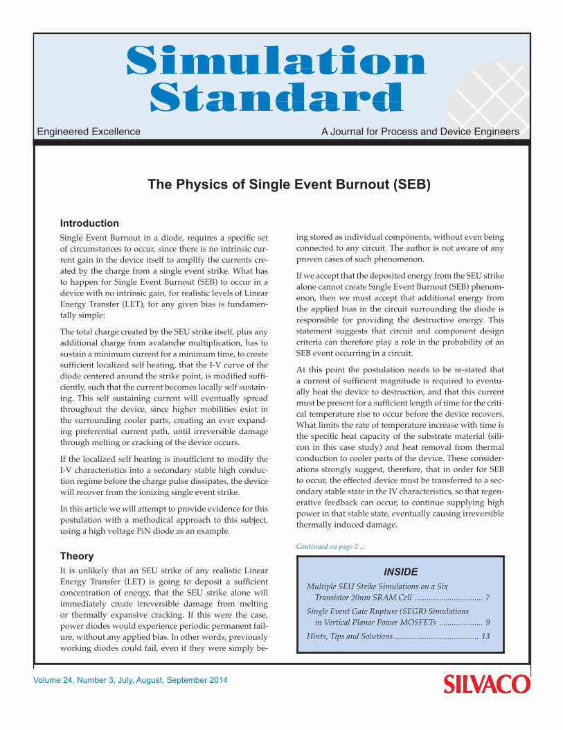
Figure 3. Time evolution snap-shots of the hole concentration during the ion strike and at 5, 50 and 150 pico-seconds after the strike.
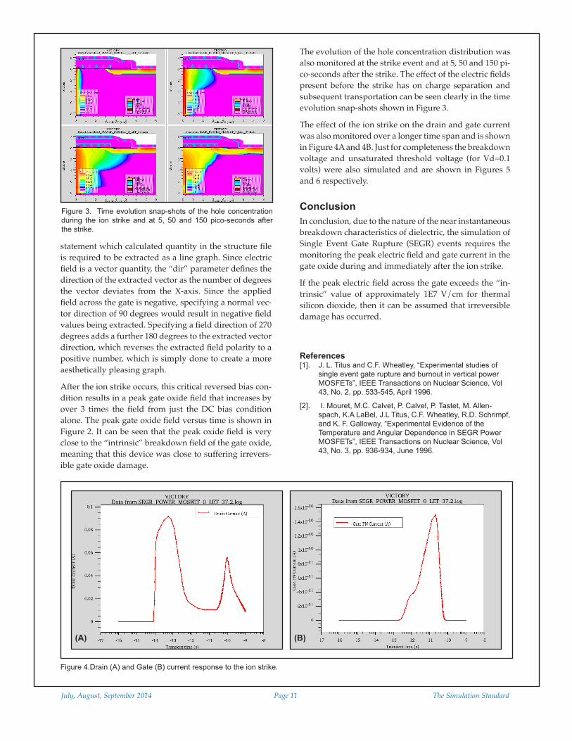
Figure 4.Drain (A) and Gate (B) current response to the ion strike.
(A) (B)
statement which calculated quantity in the structure file is required to be extracted as a line graph. Since electric field is a vector quantity, the “dir” parameter defines the direction of the extracted vector as the number of degrees the vector deviates from the X-axis. Since the applied field across the gate is negative, specifying a normal vec-tor direction of 90 degrees would result in negative field values being extracted. Specifying a field direction of 270 degrees adds a further 180 degrees to the extracted vector direction, which reverses the extracted field polarity to a positive number, which is simply done to create a more aesthetically pleasing graph.
After the ion strike occurs, this critical reversed bias con-dition results in a peak gate oxide field that increases by over 3 times the field from just the DC bias condition alone. The peak gate oxide field versus time is shown in Figure 2. It can be seen that the peak oxide field is very close to the “intrinsic” breakdown field of the gate oxide, meaning that this device was close to suffering irrevers-ible gate oxide damage.
The evolution of the hole concentration distribution was also monitored at the strike event and at 5, 50 and 150 pi-co-seconds after the strike. The effect of the electric fields present before the strike has on charge separation and subsequent transportation can be seen clearly in the time evolution snap-shots shown in Figure 3.
The effect of the ion strike on the drain and gate current was also monitored over a longer time span and is shown in Figure 4A and 4B. Just for completeness the breakdown voltage and unsaturated threshold voltage (for Vd=0.1 volts) were also simulated and are shown in Figures 5 and 6 respectively.
ConclusionIn conclusion, due to the nature of the near instantaneous breakdown characteristics of dielectric, the simulation of Single Event Gate Rupture (SEGR) events requires the monitoring the peak electric field and gate current in the gate oxide during and immediately after the ion strike.
If the peak electric field across the gate exceeds the “in-trinsic” value of approximately 1E7 V/cm for thermal silicon dioxide, then it can be assumed that irreversible damage has occurred.
References[1]. J. L. Titus and C.F. Wheatley, “Experimental studies of
single event gate rupture and burnout in vertical power MOSFETs”, IEEE Transactions on Nuclear Science, Vol 43, No. 2, pp. 533-545, April 1996.
[2]. I. Mouret, M.C. Calvet, P. Calvel, P. Tastet, M. Allen-spach, K.A LaBel, J.L Titus, C.F. Wheatley, R.D. Schrimpf, and K. F. Galloway, “Experimental Evidence of the Temperature and Angular Dependence in SEGR Power MOSFETs”, IEEE Transactions on Nuclear Science, Vol 43, No. 3, pp. 936-934, June 1996.

The Simulation Standard Page 12 July, August, September 2014
[3]. J.L Titus, C.F. Wheatley, K.M. van tyne, J.F. Krieg, D.I. Burton and A.B. Campbell, “Effect of Ion Energy Upon Dielectric Breakdown of the Capacitor Response in Verti-cal Power MOSFETs”, IEEE Transactions on Nuclear Science, Vol 45, No. 6, pp. 2492-2499, December 1998.
[4]. J.M. Lauenstein, N.Goldsman, S. Liu, J.L. Titus, R.L. Ladbury, H.S. Kim, A.M. Phan, K.A. Label, M. Zafrani, and P. Sherman, “Effects of Ion Atomic Number on Single Event Gate Rupture Susceptibility of Power Mosfets”, IEEE Transactions on Nuclear Science, Vol 58, No. 6, pp. 2628-2636, December 2011.
[5.] J.L Titus, C.F. Wheatley, D.I. Burton, I Mouret, M. Al-lenspach, J. Brews, R. Schrimpf, K. Galloway and R. L. Pease, “Impact of Oxide thickness on SEGR Failure in Vertical Power MOSFETs, Development of a Semi-Empir-ical Expression”, IEEE Transactions on Nuclear Science, Vol 42, No. 6, pp. 1928-1934, December 1995.
Figure 5. DC breakdown curve of the power MOSFET Figure 6. Unsaturated Vt curve for Vd=0.1 volts

July, August, September 2014 Page 13 The Simulation Standard
Hints, Tips and SolutionsMeshing a Non Axis Aligned SEU Beam
Figure 1a. Power MOSFET from standard example powerex15 (net doping).
Figure 1b. Power MOSFET from standard example powerex15 (mesh).
Figure 2. Basic re-mesh in Devedit on doping and the channel region – SEU beam not considered.
Q: I have an SEU beam in a 2D structure; the beam track is at an angle through the device. I don’t want to waste mesh by putting a fine mesh everywhere, is there any-way to mesh along the SEU beam track?
A: Yes, and it is quite simple to do using DevEdit’s robust feature rich meshing engine.
Figure 1a shows the Power MOSFET used in Silvaco standard example powerex15. Fig 1b shows the mesh. This structure is built in Silvaco’s 2D process simulator, Athena.
The standard example applies an SEU beam to the left hand side of the device; the meshing in this area has been refined in preparation for the application of the beam. However, the mesh shown in Figure 1b is not particular-ly good if we wanted to apply a beam diagonally across the device starting for example in the top left and exiting bottom right. This is because beam would travel through regions of coarse and moderately coarse mesh, both in the x and y directions, loosing precision.
We could apply a fine mesh across the entire substrate but this would not be very efficient. The best option would be to refine along the SEU beam track itself. To do this we can use DevEdit. DevEdit is a robust structure editing tool that can be used to create devices from scratch or it can be used to remesh existing Silvaco structures.
The meshing engine in DevEdit gives you full control over mesh placement, allowing for refinement in boxes, under regions and in specified materials for example. What it also allows you to do is to “Refine On Quanti-ties”. This means you can refine on any volume data in the structure, typically this would be Net Doping, Do-nors and Acceptors or Potential for example. However, as we can refine on any volume data in the structure file, we can refine on the Photogeneration Rate – the SEU beam.
The SEU beam information is not saved in the structure file from Athena so the first thing to do is apply the beam to the device in Atlas. Once the beam is applied and the structure saved, we can take the structure into DevEdit for re-meshing. Once remeshed in DevEdit we can pass

The Simulation Standard Page 14 July, August, September 2014
Figure 3a. SEU beam applied to the device with re-meshing on the beam track.
Figure 3b. Remeshed structure with re-meshing also undertaken on the SEU beam track.
Call for QuestionsIf you have hints, tips, solutions or questions to contribute,
please contact our Applications and Support Department Phone: +1 (408) 567-1000 Fax: +1 (408) 496-6080
e-mail: [email protected]
Hints, Tips and Solutions ArchiveCheck out our Web Page to see more details of this example
plus an archive of previous Hints, Tips, and Solutions www.silvaco.com
the structure back into Atlas for electro-optical simula-tion. All of these steps can easily be done via syntax in DeckBuild or via the various GUI’s.
Shown in Figure 2 is the power MOSFET once remeshed in DevEdit. At this point we have not meshed on the SEU beam. Re-meshing has taken place on the doping for the source and drain regions as well as under the gate oxide for channel formation. The finer mesh in these areas is quite evident.
Shown in Figure 3a is the device with the SEU beam ap-plied. Figure 3b shows the SEU beam mesh in combina-tion with the basic remesh. The diagonal track of the SEU beam is clearly indicated by the mesh. Further enhance-ment and refinement of the mesh is possible through a range of controls available to the user in DevEdit.
Here we have just shown one type of volume data that can be re-meshed in a structure, with re-meshing at the beginning of the simulation. The user can actually remesh any number of times and at any point in a simulation in both Athena and Atlas with any kind of volume data.

July, August, September 2014 Page 15 The Simulation Standard
Hints, Tips and Solutions
Figure 1. Uniform Refinement with cutaway.
Q: What Types of 3D Delaunay Shape Refinement can be used in Victory Process?
A. The Victory Process cell mode Delaunay 3D device meshing algorithm already includes various TCAD-based local refinement algorithms to ensure accurate and robust device simulation. These include junction and interface distance refinement. One benefit of these approaches is that complex refinement behavior can be specified via a simple deck interface, but a limitation is that the results can only vary according to the small num-ber of parameters of the schemes. In some cases, such as particle path refinement, it can be useful to have finer, more local control over the mesh and the shape distance refinement schemes have been produced to support this.
The new shape refinement algorithms plug into the exist-ing framework for distance-based refinement based on a scalar sizing field. All of the distance-based refinement schemes share a subset of deck syntax which controls the size of the mesh elements on or inside the particular focus geometry and the distance over which the size of the ele-ments increases to the uniform, background refinement size. The shape refinement algorithms have additional syntax which controls the parameters of the shape, such as the center of a sphere and its radius.
Examples
Syntax:
export victory(delaunay) \ structure=”delaunay_final_uniform.str” \ max.size=0.1
Figure 1 shows a simple reference cube with elements of similar, uniform size. The right-hand image shows a cut-away view where the interior of the mesh can be seen. This example provides the basis for the further refine-ment produced by the shape distance algorithms.
Syntax:
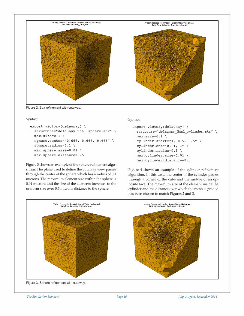
export victory(delaunay) \ structure=”delaunay_final_box.str” \ max.size=0.1 \ box.min=”0.616, 0.616, 0” \ box.max=”0.716, 0.716, 1” \ max.box.size=0.01 \ max.box.distance=0.5
Figure 2 shows the results of the box distance refinement algorithm. In this case, the axis-aligned box is defined by a pair of diagonally-opposite points which are on the boundary of the mesh. The plane defining the cutaway view passes through the center of the box. The elements on the interior of the box have a maximum size of 0.01 microns and the mesh is graded to the background size over a distance of 0.5 microns from the box.
The Simulation Standard Page 16 July, August, September 2014
Figure 2. Box refinement with cutaway.
Figure 3. Sphere refinement with cutaway.
Syntax:
export victory(delaunay) \ structure=”delaunay_final_sphere.str” \ max.size=0.1 \ sphere.center=”0.666, 0.666, 0.666” \ sphere.radius=0.1 \ max.sphere.size=0.01 \ max.sphere.distance=0.5
Figure 3 shows an example of the sphere refinement algo-rithm. The plane used to define the cutaway view passes through the center of the sphere which has a radius of 0.1 microns. The maximum element size within the sphere is 0.01 microns and the size of the elements increases to the uniform size over 0.5 microns distance to the sphere.
Syntax:
export victory(delaunay) \ structure=”delaunay_final_cylinder.str” \ max.size=0.1 \ cylinder.start=”1, 0.5, 0.5” \ cylinder.end=”0, 1, 1” \ cylinder.radius=0.1 \ max.cylinder.size=0.01 \ max.cylinder.distance=0.5
Figure 4 shows an example of the cylinder refinement algorithm. In this case, the center of the cylinder passes through a corner of the cube and the middle of an op-posite face. The maximum size of the element inside the cylinder and the distance over which the mesh is graded has been chosen to match Figures 2 and 3.

July, August, September 2014 Page 17 The Simulation Standard
Call for QuestionsIf you have hints, tips, solutions or questions to contribute,
please contact our Applications and Support Department Phone: +1 (408) 567-1000 Fax: +1 (408) 496-6080
e-mail: [email protected]
Hints, Tips and Solutions ArchiveCheck out our Web Page to see more details of this example
plus an archive of previous Hints, Tips, and Solutions www.silvaco.com
Figure 4. Cylinder refinement with cutaway.
Syntax:
export victory(delaunay) \ structure=”delaunay_final_cone.str” \ max.size=0.1 \ cone.start=”1, 0.5, 0.5” \ cone.end=”0, 1, 1” \ start.cone.radius=0.01 \ end.cone.radius=0.1 \ max.cone.size=0.01 \ max.cone.distance=0.5
Figure 5 shows the results of refinement on distance to a truncated cone. The central axis of the cone passes through a corner of the cube mesh and the center of an opposite face. This refinement scheme generalizes the cylinder approach by allowing two radii to be specified, one for each end of the cone.
ConclusionsThe shape distance refinement algorithms provide fine control over the resulting 3D Delaunay device mesh. Mul-tiple instances of each shape can be specified within the same export statement. The new refinement algorithms can be combined with the existing distance-based schemes to ensure robust and accurate device simulation.

The Simulation Standard Page 18 July, August, September 2014
Worldwide Offices: Silvaco Japan [email protected]
Silvaco [email protected]
Silvaco [email protected]
Silvaco [email protected]
Silvaco [email protected]
USA Headquarters:
Silvaco, Inc.4701 Patrick Henry Drive, Bldg. 2Santa Clara, CA 95054 USA
Phone: 408-567-1000Fax: 408-496-6080