The Next Technology Revolution - NANOTECHNOLOGY · MOTOROLA and the Stylized M Logo are registered...
38
MOTOROLA and the Stylized M Logo are registered in the US Patent & Trademark Office. All other product or service names are the property of their respective owners. © Motorola, Inc. 2003. The Next Technology Revolution - NANOTECHNOLOGY Dr. Iwona Turlik Motorola Labs
Transcript of The Next Technology Revolution - NANOTECHNOLOGY · MOTOROLA and the Stylized M Logo are registered...

MOTOROLA and the Stylized M Logo are registered in the US Patent & Trademark Office. All other product or service names are the property of their respective owners. © Motorola, Inc. 2003.
The Next Technology Revolution -NANOTECHNOLOGY
Dr. Iwona TurlikMotorola Labs

MOTOROLA and the Stylized M Logo are registered in the US Patent & Trademark Office. All other product or service names are the property of their respective owners. © Motorola, Inc. 2003.
Outline
• Background!Opportunities in Nanotechnology! Industry Trends!Nano is here – Current product implementations
• Nano as an industry disruptor
• Nano Focus Areas
• Application Opportunities (Electronics)
• Examples of Current Motorola Activities

MOTOROLA and the Stylized M Logo are registered in the US Patent & Trademark Office. All other product or service names are the property of their respective owners. © Motorola, Inc. 2003.
Nanotechnology has the potential to transform life as we know it.The ability to do things (measure, see, predict and make) on the scale of atoms and
molecules thereby making products either smaller, faster, stronger or with new properties.
– Potential for the leap into devices utilizing quantum physics.– Could enable new technologies, applications and industries never before imagined.
Nanotechnology Revolution
“Nanotechnology is the sixth truly revolutionary technologyintroduced in the modern world…” --D. Allan Bromley
Former Assistant to The President of the United States for Science and Technology (1989-1993)
“Nanotechnology is the sixth truly revolutionary technologyintroduced in the modern world…” --D. Allan Bromley
Former Assistant to The President of the United States for Science and Technology (1989-1993)
1. Industrial Revolution
2. Nuclear Energy
3. Silicon 5. Information
6. Nanotechnologyand Bio-Tech
1940s 1950s 1980s 1990s 2000s1700s 1960s4. Green

MOTOROLA and the Stylized M Logo are registered in the US Patent & Trademark Office. All other product or service names are the property of their respective owners. © Motorola, Inc. 2003.
Timeline:
1959 Richard Feynman’s speech - “There’s plenty of room at the bottom”1974 First Molecular Electronic Device patent.1981 IBM Invents scanning probe microscope: measure and identify structures
at nano-scale. Ability to move individual atoms and molecules on surface.1981 Drexel published Molecular Engineering : molecular machinery1985 Curl, Kroto, Smalley discovered buckey balls. Stable molecules that
contain 50 to 500 carbon atoms in a ball, using laser vaporized carbon.1989 IBM Almaden Research Center : wrote IBM with 35 Xenon atoms. 1991 Discovery of carbon nanotubes by Sumin Iijima at NEC Research Labs.1993 First US research lab devoted entirely to nanoscience. Smalley at Rice
University.2000 US launch of National Nano-technology Initiative (NNI)2003 President Bush signs Nanotechnology R&D act - $3.7 Billion over 4 years
History
Source: IBM
MOTOROLA and the Stylized M Logo are registered in the US Patent & Trademark Office. All other product or service names are the property of their respective owners. © Motorola, Inc. 2003.
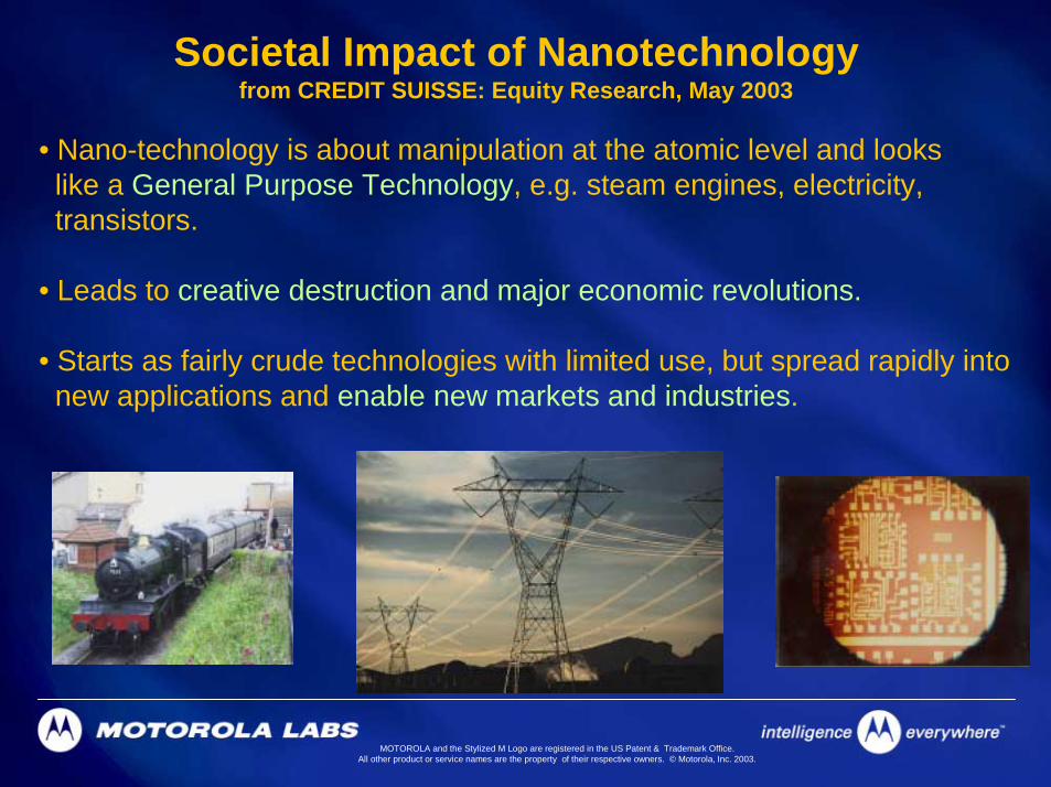
• Nano-technology is about manipulation at the atomic level and lookslike a General Purpose Technology, e.g. steam engines, electricity,transistors.
• Leads to creative destruction and major economic revolutions.
• Starts as fairly crude technologies with limited use, but spread rapidly into new applications and enable new markets and industries.
Societal Impact of Nanotechnology from CREDIT SUISSE: Equity Research, May 2003

MOTOROLA and the Stylized M Logo are registered in the US Patent & Trademark Office. All other product or service names are the property of their respective owners. © Motorola, Inc. 2003.
Nanotechnology
Agriculture
Pharmaceuticals
Energy
Environment
Materials
Electronics
Manufacturing
Transportation
NanotechnologyA technology that impacts many industries

MOTOROLA and the Stylized M Logo are registered in the US Patent & Trademark Office. All other product or service names are the property of their respective owners. © Motorola, Inc. 2003.
CURRENT Consumer Products
Nanowax: CERAX
Nano Tin Oxide: Sunscreen
Babolat VS Nanotube Drive Racquets
Nano-clay compositegas diffusion barrier
Carbon nano-tubes
Eddie Bauer
Nanotex Materials
Nano-careTM
treated fiber surface with~ 200 nm“whiskers”
Water Proof – Stain Proof
• Nano enhanced products are here!!• Migrating from niche to mainstream
consumer and industry applications

MOTOROLA and the Stylized M Logo are registered in the US Patent & Trademark Office. All other product or service names are the property of their respective owners. © Motorola, Inc. 2003.
Outline
• Background
• Nano as an industry disruptor!Example: Nano Velcro!Example: Lifetime tires!Research to products
• Nano Focus Areas
• Application Opportunities (Electronics)
• Examples of Current Motorola Activities

MOTOROLA and the Stylized M Logo are registered in the US Patent & Trademark Office. All other product or service names are the property of their respective owners. © Motorola, Inc. 2003.
NanotechnologyA Technology and Market Revolution
A truly new revolutionary technology completely disruptsMarkets, Industries and Business Models
Example Scenario in electronics industry:
What if packaging interconnects can be be replaced by a conductive CNT-Velcro based assembly process?

MOTOROLA and the Stylized M Logo are registered in the US Patent & Trademark Office. All other product or service names are the property of their respective owners. © Motorola, Inc. 2003.
Nano Velcro• Imagine manufacturing assembly without solder or adhesive
• A joint stronger than many traditional assembly methods…. and materials
• Manufactured at room temperature
Berber, Kwon, and Tomanek, Phys. Rev. Letters., Vol. 91, No 16
[13] Jean Gabriel
Nano-hooks

MOTOROLA and the Stylized M Logo are registered in the US Patent & Trademark Office. All other product or service names are the property of their respective owners. © Motorola, Inc. 2003.
Berber, Kwon, and Tomanek, Phys. Rev. Letters., Vol. 91, No 16
Michigan State University
Molecular simulation of carbon nano-velcro
Hook formed by insertion of pentagon and heptagon rings in all hexagon nano-tube
Closing
Opening
Estimated ideal pull strength = 3 GPa
Measured yield point of #1010 CR steel ~ 0.3 GPa

MOTOROLA and the Stylized M Logo are registered in the US Patent & Trademark Office. All other product or service names are the property of their respective owners. © Motorola, Inc. 2003.
Assembly Process DisruptionCurrent Electronics Assembly Process Flow
Solder reflowElectronic Components:Plastic packaging
Place electronic components
Stencil solder paste
Printed Wiring Boards:• High Tg materials• Glass-epoxy
composites
Solder reflowPlace electronic
ComponentsRoom temp. attach
Stencil solder paste
Electronics Assembly Process Flow with nano-Velcro
Electronic Components:Integrated circuit attachwith nano-Velcro
Printed Wiring Boards:• Room Tg materials• Paper, thermoplastics

MOTOROLA and the Stylized M Logo are registered in the US Patent & Trademark Office. All other product or service names are the property of their respective owners. © Motorola, Inc. 2003.
Nano Velcro Market DisruptionSolder reflow
Place electronic Components
Room temp. attach
Stencil solder pasteElectronic Components:
Integrated circuit attach
Printed Wiring Boards:• Room Tg materials• Paper, thermoplastics
Market Disruption" Create new industry: paper, textile, thermoplastic high density “PWB’s”
" Create new industry: Velcro finish electronics components
" Create new industry: Reel-to-reel, paper and textile electronics assembly" Create new industry: Ultra-thin flexible IC manufacturing to replace
traditional IC plastic packaging

MOTOROLA and the Stylized M Logo are registered in the US Patent & Trademark Office. All other product or service names are the property of their respective owners. © Motorola, Inc. 2003.
Example Scenario In Auto IndustryLifetime Tires
High wear resistance Nano elements in tires could enable OEM tires to last the lifetime of the car
Of the 250 million passenger car tires shipped in 2002, 190 million were replacement tires (MTB, RMA)
A potential innovation that completely disrupts the tire industry business model i.e., low price OEM tires and high price replacement tires

MOTOROLA and the Stylized M Logo are registered in the US Patent & Trademark Office. All other product or service names are the property of their respective owners. © Motorola, Inc. 2003.
Research to Products
Typical prerequisites:• Scalable manufacturing processes• Low cost tools for testing and evaluation• Well developed supplier base• Standards
Some disruptive nanotechnologies may be inherently scalable with very low go-to-market times
Nano will enable incremental innovation in some areas,while leading to disruptive innovation in others

MOTOROLA and the Stylized M Logo are registered in the US Patent & Trademark Office. All other product or service names are the property of their respective owners. © Motorola, Inc. 2003.
Outline
• Background
• Nano as an industry disruptor
• Industry Focus Areas!Basic Materials!Electronic Devices !Multifunctional composites
• Application Opportunities (Electronics)
• Examples of Current Motorola Activities

MOTOROLA and the Stylized M Logo are registered in the US Patent & Trademark Office. All other product or service names are the property of their respective owners. © Motorola, Inc. 2003.
Basic Nano-MaterialsIncludes manufacturing processes, characterization, metrology and standards
E.g. Carbon nano tubes, quantum dots, nano powders, etc.
NanotechnologyMajor Research Areas for Electronics Industry
MultifunctionalComposites • Self-cleaning• Color changing plastics• Self-healing• Structural materials, • ‘Aware’ materials, etc.
ElectronicDevices• Displays• OFETS• Nano pockets• Memory• Super Capacitors, etc.

MOTOROLA and the Stylized M Logo are registered in the US Patent & Trademark Office. All other product or service names are the property of their respective owners. © Motorola, Inc. 2003.
NanotechnologyCurrent Technology Focus
Nano Startups By AreaNano Publications And Patents
• Majority of nano activity is currently focused on development, characterization, metrology and standards of basic nano-materials
• Significant applications in electronic-devices and multifunctional composites are beginning to emerge
0 50 100 150
Memory Systems
Drug Delivbery
Energy
Memory displays
Software Modelling
Nanobiotech
Scanning Probes
Nanotube
Nanoparticle
Nanomaterials
Source: CREDIT SUISSE: Equity Research, May 2003
0
1000
2000
3000
4000
5000
6000
1980 1985 1990 1995 2000
Journal ArticlesPatents
Source: “Nanotechnology – Size Matters”, white paper, Institute of Nanotechnology

MOTOROLA and the Stylized M Logo are registered in the US Patent & Trademark Office. All other product or service names are the property of their respective owners. © Motorola, Inc. 2003.
Nano Materials and Suppliers
Medical electronics –diagnostics
Qdot, GE, Phillips, Siemens, etc.
Quantum dots
Thermal Substrates, heat dissipating polymers
GE, Argonide, Nanophase, Nanomat, etc.
Metal Oxides
Catalysts, soldering, welding
Argonide, Nanomat, NRC, etc.
Metals
Paint pigmentsPolymer composites
Nanocor, SW Clay Products, Bayer, Honeywell, etc.
Nano silicates
DisplaysPolymer Composites,computing, memory, sensors, fuel cells
NEC, Sumitomo, Phillips, CNI, GE, Hyperion Catalysis, Carbolex, etc.
Carbon Nano TubesApplicationsCompanyMaterials
Enablers for Devices and Applications
A Partial List

MOTOROLA and the Stylized M Logo are registered in the US Patent & Trademark Office. All other product or service names are the property of their respective owners. © Motorola, Inc. 2003.
Electronic Device Companies
1TB/sq. in. densityIBM (millipede), Seagate, HP, etc.
Data Storage
Size, performance and mobility; Pervasive computing
HP, IBM, Hitachi, Fujitsu, Intel, etc.
Nano Computer
Enabler for low power processing and memory
IBM, Intel, AMD, TI, Motorola, etc.
Transistor (Silicon and Organic)
Brighter, lower power, inexpensive displays
Motorola, Samsung, NEC, Matsushita, etc.
Displays
Universal flash memory; higher density
Nantero, HP, IBM, etc.Nano Memory
BenefitCompanyDevices
A Partial List

MOTOROLA and the Stylized M Logo are registered in the US Patent & Trademark Office. All other product or service names are the property of their respective owners. © Motorola, Inc. 2003.
Multifunctional Composite Companies
Preserves freshness. Food wrapping, beverage containers
Honeywell, PolyOne, Bayer
Nano polymer films
New functionality, fashion
Matsui, QdotColor change
Aesthetics (looks like new), longevity
Du Pont, Nano filmScratch Resistance
Cleaner surfaces, display appearance, etc.
Degussa, BASF, STO, Fraunhoffer
Self cleaning
Higher reliability; lighter weight composites, thermal stability, etc.
PolyOne, Bayer, Nanocor, Honeywell
Structural Composites(#### stiffness, #### toughness)
BenefitCompanyMacro-Application
A Partial List

MOTOROLA and the Stylized M Logo are registered in the US Patent & Trademark Office. All other product or service names are the property of their respective owners. © Motorola, Inc. 2003.
Outline
• Background
• Nano as an industry disruptor
• Industry Focus Areas
• Application Opportunities (Electronics)!Mobile Phone!Nano composites
• Examples of Current Motorola Activities

MOTOROLA and the Stylized M Logo are registered in the US Patent & Trademark Office. All other product or service names are the property of their respective owners. © Motorola, Inc. 2003.
MotorolaMotorola is engaged in several segments of the electronics and telecommunication industries
MOTOROLA and the Stylized M Logo are registered in the US Patent & Trademark Office. All other product or service names are the property of their respective owners. © Motorola, Inc. 2003.
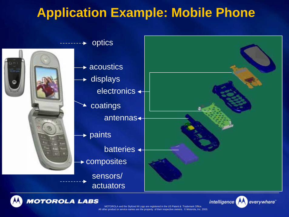
Application Example: Mobile Phone
acousticsdisplays
electronics
antennas
batteriescomposites
paints
coatings
sensors/actuators
optics

MOTOROLA and the Stylized M Logo are registered in the US Patent & Trademark Office. All other product or service names are the property of their respective owners. © Motorola, Inc. 2003.
Nano Composites: stronger, tougher, stiffer, lighter materials (adhesives, structural, electronic, optical functionality), nanobiotech for sensing, actuating, power functions
Nano antennas: Nano scale fractal antennas for multiple spectra and broadband
Nanodisplays: Large, lower cost and brighter displays based on embedded carbon nanotubes
Nano power: High capacity power sources (storage, conversion, advanced fuel cells, photonic energy), parasitic energy harvesting, nanobiotech related functionality
Some applications and benefits of Nanotechnology

MOTOROLA and the Stylized M Logo are registered in the US Patent & Trademark Office. All other product or service names are the property of their respective owners. © Motorola, Inc. 2003.
Nano Composites• A phone housing requires stiffness, toughness, moldability,
paintability, surface finish, flame retardance, chemical resistance and thermal stability, recyclability, etc.
• Traditional engineering design is often a compromise of these competing requirements
• Nano materials enable application-specific, tailored material design
e.g:CNTs and Nano-silicates

MOTOROLA and the Stylized M Logo are registered in the US Patent & Trademark Office. All other product or service names are the property of their respective owners. © Motorola, Inc. 2003.
Compared to current phone housing, nano materials will have:
• High Strength• High Stiffness• High Toughness • Multifunctionality, etc.
Nano materials for tailored composites
Extremely flexible (reversible)
Deformation Mode:Stone-Wales Transf: Heptagon.
J Chem Phys Vol 104 No 5 1996
1280
207
24 2.1
40
0.46 0.4 0.0550
200
400
600
800
1000
1200
1400
CNT Steel Nylon PC
Mod
ulus
(GPa
)
0
10
20
30
40
50
60
Bre
ak S
tren
gth
(GPa
)ModulusBreak strength
J Chem Phys Vol 104 No 5 1996

MOTOROLA and the Stylized M Logo are registered in the US Patent & Trademark Office. All other product or service names are the property of their respective owners. © Motorola, Inc. 2003.
CNT can be metallic or semiconducting, depending on chirality
Metal
Semiconductor
Metal
Current Carrying Capacity
SWNT: 109 A/cm2
Copper wire : 106 A/cm2 (burns)
Field Emission: Excellent field emitter; high aspect ratio and small tip radius of curvature are ideal for field emission.
• SWNT Radius 0.6 to 1.8 nanometers
E max∝∝∝∝ V / RAt 30 V concentrated electric
field ~ 107 to 108 V/cm
Nano materials for tailored composites

MOTOROLA and the Stylized M Logo are registered in the US Patent & Trademark Office. All other product or service names are the property of their respective owners. © Motorola, Inc. 2003.
Polymer is compatabalized with nano-silcate
Molecular Simulation
Si Tetrahedron
Al Octahedron
1 nm
Simulation from: Hacket, Mania and Giannelis,Chem. Mater. 2000, 12,2161-2167
Nano-silicates: a natural nano-material
Expands to ~ 20 Å
Cretaceous (85-125 M Years)
Nano Silicate Polymer Composites

MOTOROLA and the Stylized M Logo are registered in the US Patent & Trademark Office. All other product or service names are the property of their respective owners. © Motorola, Inc. 2003.
in-situ nano-silicate polymerization
Nylon Synthesis
Significant macro-property improvements.A little goes a long way !
Nylon Synthesis
Nylon 6 Nano-Composite2.1 (1.9x)1.4
(1.3x)1.1Elastic Modulus(GPa)
115 (1.6x)
62 (0.9x)72
Tensile Strength (MPa)
Nylon 6 Clay Nano Composite 4 wt %
Nylon 6 Glass
Filled 20 wt %
Nylon 6 Un-Reinforced
Nano Silicate Polymer Composites
• Nano materials enables unprecedented opportunities to tailor macro-properties.• Key driver is interfacial effects versus weighted average of traditional fillers.
Source: Nanocor Inc.

MOTOROLA and the Stylized M Logo are registered in the US Patent & Trademark Office. All other product or service names are the property of their respective owners. © Motorola, Inc. 2003.
Outline
• Background
• Nano as an industry disruptor
• Industry Focus Areas
• Application Opportunities (Electronics)
• Examples of Current Motorola Activities!Organic Transistors!Displays!Self-healing!Standards

MOTOROLA and the Stylized M Logo are registered in the US Patent & Trademark Office. All other product or service names are the property of their respective owners. © Motorola, Inc. 2003.
Gate
Source Drain
Dielectric
Nanoelements of an OST
Nanocomposite oxides, direct-assembly dielectric
Nanoscale ordering in semiconductor material at charge injection interface
SemiconductorChannel
Nanoparticle suspensions

MOTOROLA and the Stylized M Logo are registered in the US Patent & Trademark Office. All other product or service names are the property of their respective owners. © Motorola, Inc. 2003.
CRT is a vacuum tube in which
CRT - electrons from three cathodes are scanned across screen
Nano Emissive Display Selective growth Selective growth only on padsonly on pads
NED electrons from millions of carbon Nanotubes travel to a screen
Millions of cathodes enable a thin, high clarity flat screen TV

MOTOROLA and the Stylized M Logo are registered in the US Patent & Trademark Office. All other product or service names are the property of their respective owners. © Motorola, Inc. 2003.
Active Regulation
Reactive Materials
Mesoporous Networks
Adaptive Fluids/Solids
Self-RegulatingFunction
Self-GeneratingFunction
Self-Healing Materials, Inspired by BiologyCreating a Synthetic Autonomic System

MOTOROLA and the Stylized M Logo are registered in the US Patent & Trademark Office. All other product or service names are the property of their respective owners. © Motorola, Inc. 2003.
Self-Healing Materials
Brown et al., Exp. Mech., 2002
> 90% strength recovery
0
10
20
30
40
50
60
0 250 500 750 1000 1250 1500
Load
(N)
Displacement ( µµµµm)
η = 90.3%η = 90.3%η = 90.3%η = 90.3%Virgin
Healed
White et al., Nature 2001
Today
Self-healing Functionality: The ability to repair damage automatically without manual intervention.
Collaboration with Prof. Nancy SottosTAM Dept. & Beckman Institute for Advanced Science and TechnologyNano can enable
self-assembled nano-containers:
Self-heal at nano scale
Micronscale
Fan et al., Nature 2000Lu, et al., Nature 2001

MOTOROLA and the Stylized M Logo are registered in the US Patent & Trademark Office. All other product or service names are the property of their respective owners. © Motorola, Inc. 2003.
Motorola Chairing IEEE Nanotechnology Working Group
Draft Standard Test Methods for Measurement of Electrical Properties of Carbon Nanotubes (P1650TM)
http://grouper.ieee.org/groups/1650

MOTOROLA and the Stylized M Logo are registered in the US Patent & Trademark Office. All other product or service names are the property of their respective owners. © Motorola, Inc. 2003.
IEEE Nanotechnology Standards Roadmap Workshop - Standardization Along the Path from R&D to Commercialization
Workshop Held on 11/5/03 –90 Registrants from Industry, Academia and International Labs
IEEE Workshop to Create a Standards Roadmap for Nanoelectronics -materials, devices, and systems
http://grouper.ieee.org/groups/nano
MOTOROLA and the Stylized M Logo are registered in the US Patent & Trademark Office. All other product or service names are the property of their respective owners. © Motorola, Inc. 2003.
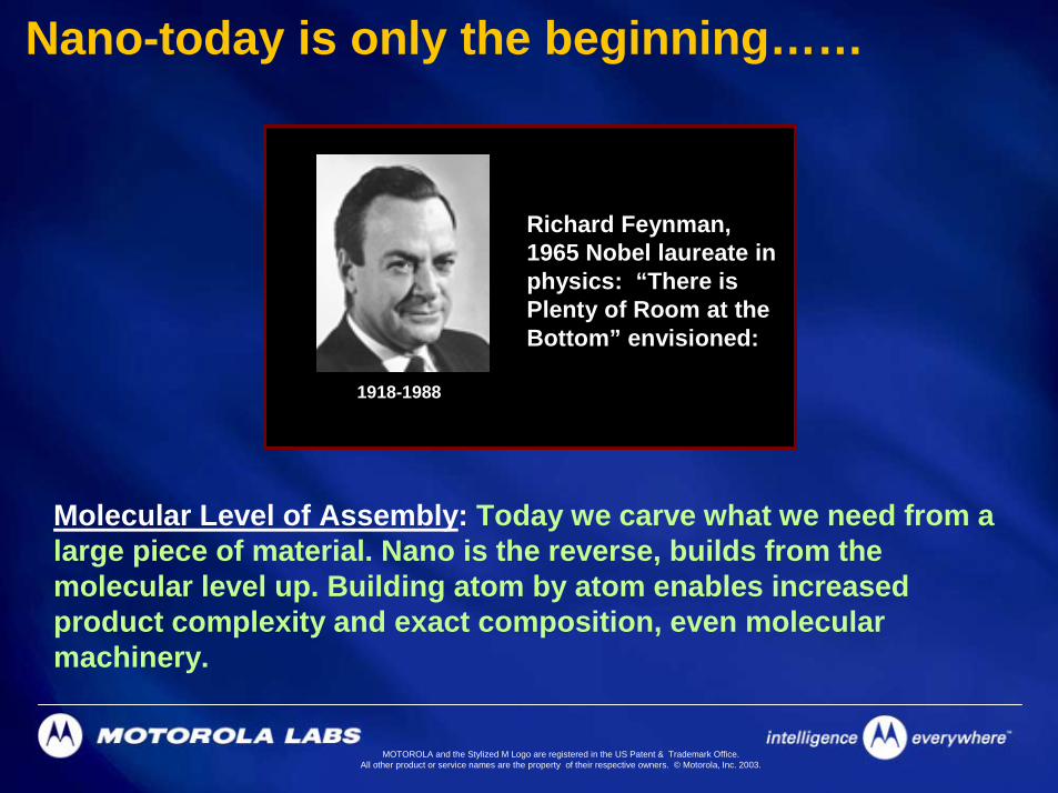
Nano-today is only the beginning……
Richard Feynman, 1965 Nobel laureate in physics: “There is Plenty of Room at the Bottom” envisioned:
1918-1988
Molecular Level of Assembly: Today we carve what we need from a large piece of material. Nano is the reverse, builds from the molecular level up. Building atom by atom enables increased product complexity and exact composition, even molecular machinery.