
the journal - nutwooduk.co.uk
32
journal Issue 92 January 2011 ISSN 1748-9253 the Bench testing individual PCB’s for immunity By Keith Armstrong. See Page 24 CE Marking of Defence Equipment A Report by David Imeson. See Page 10 GASTEC at CRE Ltd Buy Blackwood Compliance Laboratories See Page 9 EMCUK 2011... 8 th Successful Year 11/12 th October The Racecourse, Newbury... so easy to get to For Industry, By Industry. It’s where everyone who is anyone in EMC comes to Network and do real Business... definitely not to be missed. See Page 9
Transcript of the journal - nutwooduk.co.uk

1
journalIssue 92 January 2011
ISSN 1748-9253
the
Bench testing individual PCB’s for immunityBy Keith Armstrong. See Page 24CE Marking of Defence EquipmentA Report by David Imeson. See Page 10
GASTEC at CRE Ltd Buy Blackwood Compliance
LaboratoriesSee Page 9
EMCUK 2011... 8th Successful Year11/12th October
The Racecourse, Newbury... so easy to get to
For Industry, By Industry.It’s where everyone who is anyone in EMCcomes to Network and do real Business...
definitely not to be missed.See Page 9

2

3 The EMC Journal January 2011
What's In This Issue
24
5
Every effort has been made to ensure that the information given in this Journal is accurate, but no legal responsibility is accepted for any errors, omissions or misleading statements in that informationcaused by negligence or otherwise, and no responsibility is accepted in regard to the standing of any firms, companies or individuals mentioned or for any advice or information given by them.
News and Information
EMCIA News
GASTEC at CRE Ltd buy Blackwood ComplianceLaboratories
EMCUK 2011, 11/12 October, The Racecourse,Newbury
CE Marking of Defence EquipmentA Report by David Imeson
Banana Skins
16
30
12
18
22
the journal
www.theemcjournal.com www.emcia.org www.emcuk.co.uk www.emcacademy.org
John Woodgate’s Column
Product Gallery
The GTEM Test Chamber, Practical AspectsBy Jonathan Hamilton, Megger Instruments Ltd
Bench testing individual PCB’s for immunityBy Keith Armstrong, Cherry Clough Consultants
Advertisers Index
5
9
9
10

4The EMC Journal January 2011

5 The EMC Journal January 2011
News
The EMC JournalFree to readers worldwide
January 2011- Issue No. 92Published every other month
First Issue March 1995
Editorial & Publishing Director:Alan E Hutley
Technical Consultant:Dave Fynn
Advertisement Sales Director:Lynne S Rowland
Front Cover
Hero image, EMCUK 2011, page 9Circle top, Rohde & Schwarz, page 19Circle middle, DEM Manufacturing, page 20Circle bottom, AR, page 20
Secretariat for EMCIA
The Trade Association for the EMC Industry.Web: www.emcia.org
Production & Circulation Director:Pam A Hutley
Nutwood UK LtdEddystone Court, De Lank Lane,
St. Breward, Bodmin, Cornwall PL30 4NQTel: +44 (0)1208 851530Fax: +44 (0)1208 851630
Web: www.theemcjournal.com© Nutwood UK Limited January 2011
Cranage EMC Testing Ltd is pleased toannounce its’ appointment as a Notified Bodyunder Article 11 of the Low Voltage Directive(LVD) (Directive 2006/95/EC)
The Company’s appointment has beenconfirmed by the Secretary of State for thepurposes of issuing reports of conformity andgiving opinions in relation to the followingelectrical equipment:
• Audio, Video and Similar ElectronicApparatus
• Household and Similar ElectricalAppliances
• IT and Telecommunications Equipment
• Measurement, Control and LaboratoryEquipment
Established in 1992, Cranage is a name thatis well known in the West Midlands forproviding laboratory testing services forproduct manufacturers and importers in thesurrounding areas of Cheshire, Shropshire,Staffordshire, Merseyside and GreaterManchester.
UKAS accredited facilities for product safetyinclude testing to EN60950, EN61010,EN60065, EN60335 with many morestandards in the range being covered on anon-accredited basis to meet the requirements
of its customers.
The ethos behind Cranage was to providecustomers with a genuine alternative, a testhouse that could offer testing services to suitall budgets whilst also being run by a teamof highly qualified and experienced technicalstaff. With the flexibility to provide a totalproduct testing solution which encompassesany mix of standards and tests to suittechnical and budgetary requirements,Cranage is well placed to meet the challengesof the current and future economic climates.
For more information please visit our websitewww.cranage.co.uk.
Cranage appointed Notified Body for LVD Directive
EMCIA News...Christmas Meeting
This event has firmly established itself as one of the mostenjoyable of the year, which was endorsed by the high turnoutof members.
John Terry, HITEK Electronic Materials Ltd, gave aninteresting presentation on 35 years in EMC. This wasfollowed by Keith Hodgkinson, Head of Electronics & IT,BIS. We were delighted that despite the huge pressure ofwork within BIS, that Keith agreed to join us for a veryinteresting presentation and lunch. This is the second timeKeith has attended our EMCIA Christmas meeting and wecertainly hope it will not be the last.
A presentation of two interesting books on organ music waspresented to Malcolm Charsley, ETS-Lindgren Ltd, on hisretirement. Malcolm has been a staunch supporter of EMCIA
and we are pleased to say although retiring he hopes to keephis hand in and will be welcome back as a guest at any time.
John Davies of Blackwood Compliance Laboratories has soldto GASTEC at CRE Ltd, see full details on page 9.
Smart Grid/Metering. EMCIA have been requested via EKTNto submit proposals to Smart Energy Special Interest Groupof the Technology Strategy Board (SESIG). Richard Marshallis the lead member.
If you are interested in joining the EMCIA, please send anemail to [email protected].
The next meeting is the AGM on 5th April, venue to beannounced.
6
News and Information
The EMC Journal January 2011
Testing and certification organisation YorkEMC Services (YES) has completed theexpansion of its operations in the South Westof England.
The company has just unveiled its brand newcompliance laboratory in Yate, SouthGloucestershire during an official openingceremony at the site conducted by SteveWebb, Minister of State for Pensions andlocal MP for Thornbury and Yate.
“I am delighted to welcome a new employerto Yate, and especially one that is obviouslya leader in its field. I am sure that theimpressive scientific and engineering workthat the company undertakes for localindustry will also be of interest to localstudents and young people and I hope to workwith the company to forge strong links withthe local community in the coming years”
The purpose built laboratory offers anextensive range of compliance services underone roof, ideally located close to Bristol andthe M4/M5 motorway network providing alocal testing solution within travellingdistance for customers in the region.
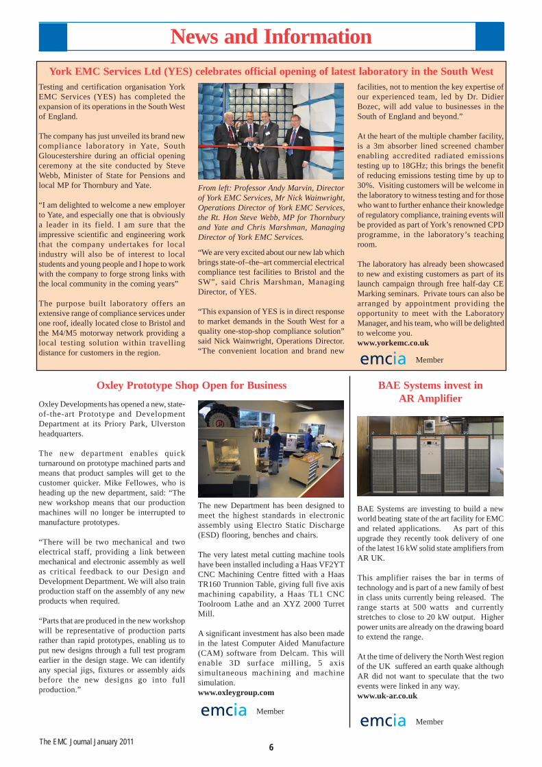
From left: Professor Andy Marvin, Directorof York EMC Services, Mr Nick Wainwright,Operations Director of York EMC Services,the Rt. Hon Steve Webb, MP for Thornburyand Yate and Chris Marshman, ManagingDirector of York EMC Services.
York EMC Services Ltd (YES) celebrates official opening of latest laboratory in the South West
“We are very excited about our new lab whichbrings state-of–the–art commercial electricalcompliance test facilities to Bristol and theSW”, said Chris Marshman, ManagingDirector, of YES.
“This expansion of YES is in direct responseto market demands in the South West for aquality one-stop-shop compliance solution”said Nick Wainwright, Operations Director.“The convenient location and brand new
facilities, not to mention the key expertise ofour experienced team, led by Dr. DidierBozec, will add value to businesses in theSouth of England and beyond.”
At the heart of the multiple chamber facility,is a 3m absorber lined screened chamberenabling accredited radiated emissionstesting up to 18GHz; this brings the benefitof reducing emissions testing time by up to30%. Visiting customers will be welcome inthe laboratory to witness testing and for thosewho want to further enhance their knowledgeof regulatory compliance, training events willbe provided as part of York’s renowned CPDprogramme, in the laboratory’s teachingroom.
The laboratory has already been showcasedto new and existing customers as part of itslaunch campaign through free half-day CEMarking seminars. Private tours can also bearranged by appointment providing theopportunity to meet with the LaboratoryManager, and his team, who will be delightedto welcome you.www.yorkemc.co.uk
Oxley Developments has opened a new, state-of-the-art Prototype and DevelopmentDepartment at its Priory Park, Ulverstonheadquarters.
The new department enables quickturnaround on prototype machined parts andmeans that product samples will get to thecustomer quicker. Mike Fellowes, who isheading up the new department, said: “Thenew workshop means that our productionmachines will no longer be interrupted tomanufacture prototypes.
“There will be two mechanical and twoelectrical staff, providing a link betweenmechanical and electronic assembly as wellas critical feedback to our Design andDevelopment Department. We will also trainproduction staff on the assembly of any newproducts when required.
“Parts that are produced in the new workshopwill be representative of production partsrather than rapid prototypes, enabling us toput new designs through a full test programearlier in the design stage. We can identifyany special jigs, fixtures or assembly aidsbefore the new designs go into fullproduction.”
The new Department has been designed tomeet the highest standards in electronicassembly using Electro Static Discharge(ESD) flooring, benches and chairs.
The very latest metal cutting machine toolshave been installed including a Haas VF2YTCNC Machining Centre fitted with a HaasTR160 Trunnion Table, giving full five axismachining capability, a Haas TL1 CNCToolroom Lathe and an XYZ 2000 TurretMill.
A significant investment has also been madein the latest Computer Aided Manufacture(CAM) software from Delcam. This willenable 3D surface milling, 5 axissimultaneous machining and machinesimulation.www.oxleygroup.com
Oxley Prototype Shop Open for Business
BAE Systems are investing to build a newworld beating state of the art facility for EMCand related applications. As part of thisupgrade they recently took delivery of oneof the latest 16 kW solid state amplifiers fromAR UK.
This amplifier raises the bar in terms oftechnology and is part of a new family of bestin class units currently being released. Therange starts at 500 watts and currentlystretches to close to 20 kW output. Higherpower units are already on the drawing boardto extend the range.
At the time of delivery the North West regionof the UK suffered an earth quake althoughAR did not want to speculate that the twoevents were linked in any way.www.uk-ar.co.uk
BAE Systems invest inAR Amplifier
Member
Member Member

7
8
News and Information
The EMC Journal January 2011
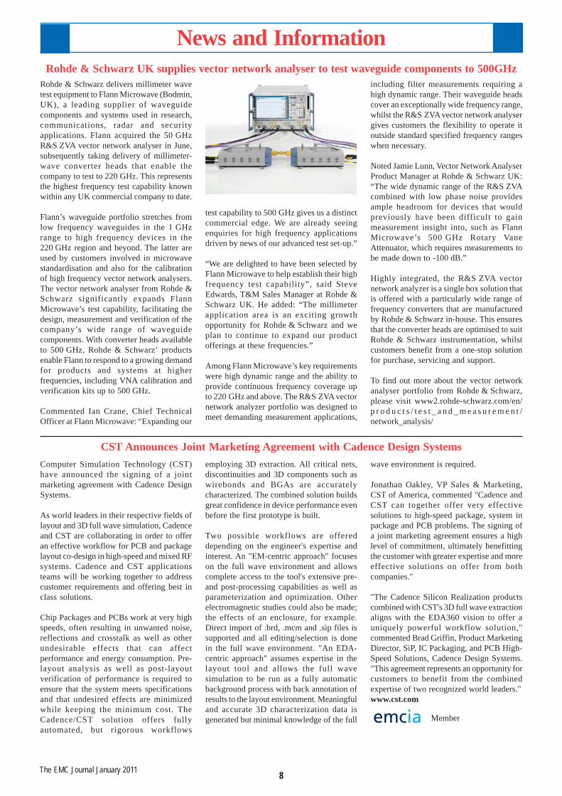
test capability to 500 GHz gives us a distinctcommercial edge. We are already seeingenquiries for high frequency applicationsdriven by news of our advanced test set-up.”
“We are delighted to have been selected byFlann Microwave to help establish their highfrequency test capability”, said SteveEdwards, T&M Sales Manager at Rohde &Schwarz UK. He added: “The millimeterapplication area is an exciting growthopportunity for Rohde & Schwarz and weplan to continue to expand our productofferings at these frequencies.”
Among Flann Microwave’s key requirementswere high dynamic range and the ability toprovide continuous frequency coverage upto 220 GHz and above. The R&S ZVA vectornetwork analyzer portfolio was designed tomeet demanding measurement applications,
Rohde & Schwarz UK supplies vector network analyser to test waveguide components to 500GHzincluding filter measurements requiring ahigh dynamic range. Their waveguide headscover an exceptionally wide frequency range,whilst the R&S ZVA vector network analysergives customers the flexibility to operate itoutside standard specified frequency rangeswhen necessary.
Noted Jamie Lunn, Vector Network AnalyserProduct Manager at Rohde & Schwarz UK:“The wide dynamic range of the R&S ZVAcombined with low phase noise providesample headroom for devices that wouldpreviously have been difficult to gainmeasurement insight into, such as FlannMicrowave’s 500 GHz Rotary VaneAttenuator, which requires measurements tobe made down to -100 dB.”
Highly integrated, the R&S ZVA vectornetwork analyzer is a single box solution thatis offered with a particularly wide range offrequency converters that are manufacturedby Rohde & Schwarz in-house. This ensuresthat the converter heads are optimised to suitRohde & Schwarz instrumentation, whilstcustomers benefit from a one-stop solutionfor purchase, servicing and support.
To find out more about the vector networkanalyser portfolio from Rohde & Schwarz,please visit www2.rohde-schwarz.com/en/p r o d u c t s / t e s t _ a n d _ m e a s u r e m e n t /network_analysis/
Rohde & Schwarz delivers millimeter wavetest equipment to Flann Microwave (Bodmin,UK), a leading supplier of waveguidecomponents and systems used in research,communications, radar and securityapplications. Flann acquired the 50 GHzR&S ZVA vector network analyser in June,subsequently taking delivery of millimeter-wave converter heads that enable thecompany to test to 220 GHz. This representsthe highest frequency test capability knownwithin any UK commercial company to date.
Flann’s waveguide portfolio stretches fromlow frequency waveguides in the 1 GHzrange to high frequency devices in the220 GHz region and beyond. The latter areused by customers involved in microwavestandardisation and also for the calibrationof high frequency vector network analysers.The vector network analyser from Rohde &Schwarz significantly expands FlannMicrowave’s test capability, facilitating thedesign, measurement and verification of thecompany’s wide range of waveguidecomponents. With converter heads availableto 500 GHz, Rohde & Schwarz’ productsenable Flann to respond to a growing demandfor products and systems at higherfrequencies, including VNA calibration andverification kits up to 500 GHz.
Commented Ian Crane, Chief TechnicalOfficer at Flann Microwave: “Expanding our
Computer Simulation Technology (CST)have announced the signing of a jointmarketing agreement with Cadence DesignSystems.
As world leaders in their respective fields oflayout and 3D full wave simulation, Cadenceand CST are collaborating in order to offeran effective workflow for PCB and packagelayout co-design in high-speed and mixed RFsystems. Cadence and CST applicationsteams will be working together to addresscustomer requirements and offering best inclass solutions.
Chip Packages and PCBs work at very highspeeds, often resulting in unwanted noise,reflections and crosstalk as well as otherundesirable effects that can affectperformance and energy consumption. Pre-layout analysis as well as post-layoutverification of performance is required toensure that the system meets specificationsand that undesired effects are minimizedwhile keeping the minimum cost. TheCadence/CST solution offers fullyautomated, but rigorous workflows
employing 3D extraction. All critical nets,discontinuities and 3D components such aswirebonds and BGAs are accuratelycharacterized. The combined solution buildsgreat confidence in device performance evenbefore the first prototype is built.
Two possible workflows are offereddepending on the engineer's expertise andinterest. An "EM-centric approach" focuseson the full wave environment and allowscomplete access to the tool's extensive pre-and post-processing capabilities as well asparameterization and optimization. Otherelectromagnetic studies could also be made;the effects of an enclosure, for example.Direct import of .brd, .mcm and .sip files issupported and all editing/selection is donein the full wave environment. "An EDA-centric approach" assumes expertise in thelayout tool and allows the full wavesimulation to be run as a fully automaticbackground process with back annotation ofresults to the layout environment. Meaningfuland accurate 3D characterization data isgenerated but minimal knowledge of the full
wave environment is required.
Jonathan Oakley, VP Sales & Marketing,CST of America, commented "Cadence andCST can together offer very effectivesolutions to high-speed package, system inpackage and PCB problems. The signing ofa joint marketing agreement ensures a highlevel of commitment, ultimately benefittingthe customer with greater expertise and moreeffective solutions on offer from bothcompanies."
"The Cadence Silicon Realization productscombined with CST's 3D full wave extractionaligns with the EDA360 vision to offer auniquely powerful workflow solution,"commented Brad Griffin, Product MarketingDirector, SiP, IC Packaging, and PCB High-Speed Solutions, Cadence Design Systems."This agreement represents an opportunity forcustomers to benefit from the combinedexpertise of two recognized world leaders."www.cst.com
CST Announces Joint Marketing Agreement with Cadence Design Systems
Member
9 The EMC Journal January 2011
News and Information
Blackwood Compliance Laboratories, theaward-winning team of complianceprofessionals dedicated to providing aneffective, efficient and accurate testingservice has been bought by GASTEC at CRELimited of Cheltenham.
With the Blackwood emphasis very much oncustomer satisfaction with friendlinessensuring repeat business, there was a veryneat fit into the Cheltenham company – itselfalready a Notified Body under the GasAppliance, Construction Products and BoilerEfficiency Directives.
Business Area Manager for Product Testing,James Verlaque, said “over the years we haveinvested heavily in extending the scope ofour accreditations, including electrical safetytesting; our aim has always been to try toprovide a one-stop solution for our clients,but EMC was always elusive to us. Then wediscovered Blackwood and found them first
class in every respect: technical knowledge,customer service, cost and quality were all‘spot-on’. So in the words of a famousadvertisement, ‘we liked it so much webought the Company!’”.
It is very much business as usual atBlackwood as they settle into their newposition within the GaC business. PaulGwilliam, who has been involved in EMCtesting at Blackwood since 1996, remains asLaboratory Manager and controls the day-to-day operations of all laboratories (EMC,Safety and EMF). Paul says “We are reallyexcited about this latest development in theBlackwood story. We look forward toworking within the GaC business and theopportunities presented by joining the Kiwagroup.”
Paul is ably supported by Ginnie Baker theQuality Manager who has been involved in
laboratory quality issues for both productcompliance testing and test equipmentcalibration since 1998 and is responsible forensuring that Blackwood Labs follow therequirements of ISO 17025:2005 – theinternational quality standard for test andcalibration laboratories.
John Davies steps down as ManagingDirector having been involved in productcompliance testing since 1990. John is aninternationally recognised expert on EMCmatters and remains actively involved withBlackwood on a consultancy basis.
The business will operate as a wholly-ownedsubsidiary of GaC, itself wholly owned bythe Kiwa group of the Netherlands.www.gastecuk.comwww.blackwood-labs.co.uk
New acquisition extends laboratory capability
Member
EMCUK 2011... 8th Successful Year11/12th October
The Racecourse, Newbury... so easy to get toFor Industry, By Industry.
It’s where everyone who is anyone in EMC comes to Network and do real Business... definitely not to be missed.
If you are interested in making a contribution/presentation then please email your ideas to [email protected] can then be discussed with the steering committee.
Topics will be very varied and may include: Electromagnetics, Defence, Aerospace, Consumer Electronics, Luminaires andLighting, Electric Vehicles, Smart Grid, Smart Metering, Audio to name just a few.
This year we are continuing with the development of a more hands on workshop approach and hopefully sessions on “how tomake your project work”.
Steering Committee... the very best within the EMC Industry.
Keith Armstrong CEngFIET SMIEEE ACGI
Cherry CloughConsultants Ltd
Professor Nigel CarterSMIEEE EMP FellowSUMMA Foundation
Consultant
Paul Duxbury BEngPresident EMCIA
Chairman IEEE EMC-SUKRI ChapterCST UK Ltd
Ian MacDiarmid BEngMSc MBA CEng FIET
Chairman IETElectromagnetics TPN
BAE Systems, Military AirSolutions (MAS)
Tim Williams BScElmac Services
Workshop/Conference... would you like to contribute?
www.emcuk.co.uk

10The EMC Journal January 2011
News and Information
EMCTLA and TRaC jointly ran a seminaron the CE Marking of Military Equipmenton 11th Jan 2011. Setting the scene TRaC’sSteve Hayes said the widespread view thatmilitary equipment was automaticallyexcluded from civilian directives was basedon the 1958 list of munitions of war andarticle 296 of the Treaty of Amsterdam (nowarticle 346 of the Treaty of Lisbon). This viewwas overturned by the 2006 European Courtof Justice ruling which stated that:
“it is for the member state which seeks torely on Article 296 TEC to furnishevidence that the exemptions in questiondo not go beyond the limits of suchclearly defined cases”,
and added:
“Derogation cannot be consideredautomatic”.
As a result the Commission has publishedan explanatory document COM (2006) 799which is very specific and concludes that theexemptions are very few and have to beassessed on a case-by-case basis by thecontracting authority. It states the need toevaluate:
• Which essential security interest isconcerned?
• What is the connection between thissecurity interest and the specificprocurement decision?
• Why is the non-application of the PublicProcurement Directive in this specificcase necessary for the protection of thisessential security interest?
More recently the Defence ProcurementDirective 2009/81/EC of 13 July 2009 has
been published. This concerns the gradualestablishment of a European defenceequipment market and as a prerequisite anappropriate legislative framework. ThisDirective has profound implications onMembers States procurement of Defenceequipment and services. The UK MOD hasissued its own clarification in DEF STAN 59-411 Part 1, Annex F.
The seminar on the 11th Jan was occasionedby the publication of Guide to EMCDirective conformity of equipmentdesigned for military purposes CLCTR50538:2010 which was written byCENELEC TC210 WG(9) with significantinput from the EMCTLA. Pete Dorey, TUVPS used this document as the basis of hispaper “Introduction to the CENELEC Guideto EMC Directive conformity of equipmentdesigned for military purposes”. Thisdocument provides guidance tomanufacturers and outlined the three 3different routes to compliance using bothmilitary and civilian standards.
Although EMC is clearly a key directive thisseminar covered the whole scope of relevantnew approach directives some of which applyto military equipment and others do not. Fornaval vessels Kim Fisher, BABT provideda paper that showed the answer is neversimple and straightforward. His answer inbrief was “not applicable but..”.
Simon Barrowcliff, TRaC covered thesafety directives Machinery, LVD and ATEXwhich definitely are applicable. In the UKthe Health & Safety at Work Act (HASAWA)and the Provision and Use of WorkEquipment Regulations (PUWER) mandatethat safety must be a primary concern. Simoncovered these directives in some detail withmany specific examples.
The Challenges for UK Defencemanufacturers were considered by RichardHoad, Qinetiq. He said that there was a lackof clarity in the formal guidance and that UKmanufacturers are disadvantaged comparedto their European counterparts since in somecountry’s military equipment is stillconsidered exempt.
A directive that does exempt defenceequipment is the R&TTE which was coveredby Barry Cartman, Cartman dot org. Hegave a detailed presentation on the changescurrently being drafted and explained thatbeing excluded form the R&TTE merely puta lot of equipment back into the EMCD andLVD.
The Automotive requirements for MilitaryVehicles were covered by Rob Ward,Millbrook who said that vehicles - at leastin the UK – must meet, as far as possible, allroad vehicle legislation.
Vic Clements, Oakmead Consultingreviewed the WEEE and RoHS directiveswhich have specific exclusions for militaryequipment but these exclusions only apply ifthe equipment is designed solely for militarypurposes.
At the end of the day it was clear that thereare still many questions to answer. Probablythe main one is to define Military Equipmentand resolve the fact that it is included in somedirectives and excluded in others. The othermajor problem is the lack of a level playingfield with tight controls in the UK andGermany totally excluding militaryequipment in their directive legislation. Sothe final conclusion of the day was that thereis much more to debate with one key objectiveof raising these issues at the right level withthe EU Parliament to get the clarification soneeded across the EU.
David Imeson BSc, CEng, MIEE
Dave has have worked in the electronicsindustry for more than 35 years, first forTexas Instruments, then 27 years in IBM;latterly as an independent consultant runninghis own company, Compliance Europe Ltdand with Hursley EMC Services
As Chairman of the EMC Notified Bodies(ECANB) he was a member of the SLIMWorking Group responsible for the revisionof the EMC Directive now published as 2004/108 and also editor of the group that producedthe Guidelines to the new directive. He alsorepresents them on the EU Commission EMCWorking Party
In the UK, he is responsible for the operationof the EMC Test Laboratory Association(EMCTLA) which coordinates the technicalactivities of the EMC test labs.
He is also on the BSI EMC CommitteesGEL210, 210/11 and 210/12 as well asconvenor of CENELEC WG(9) responsiblefor the EMC guide for testing militaryequipment.
CV for David Imeson BSc, CEng, MIEE.
Dave can be contacted at:Tel: +44 (0) 1794 323382Email: [email protected]
CE Marking of Defence EquipmentReport by David Imeson EMCTLA
Dave Imeson

11 The EMC Journal January 2011
News and Information
Multi-million pound sales in India and China,major orders in three other Asia-Pacificmarkets and support from UK Trade andInvestment (UKTI), were crucial factors inhelping St-Helens based Rainford EMCSystems survive reduced sales to UK andEuropean markets during 2009.
Rainford EMC Systems design, manufactureand install a range of shielded enclosures totest products for electromagnetic emissions,and were referred to UKTI’s StrategicAlliance Service (SAS) in 2007 for adviceon market entry options following initialdiscussions with a potential Indian partner.
SAS, funded by the North West RegionalDevelopment Agency (NWDA) and deliveredby UKTI, provides practical assistance tohelp manufacturing and service sectorcompanies with complex procedures such asManufacturing under Licence (MUL),Overseas Joint Venture (JV) and ForeignDirect Investment (FDI)
Julian Birchett, UKTI’s SAS Adviser, metRainford EMC Systems’s senior managementteam to review the importance ofinternational trade to the business as thecompany was heavily dependent on UK andEuropean markets at the time. With SASmentoring and support a strategy wasformulated to develop a relationship with a
major strategic partner to target two emergingmarkets (India and China).
Julian says: “The company had previouslyconcluded an agreement with an Indianpartner specialising in military sales but wasnot optimising penetration of the largecivilian applications market. It had alsoconcluded an agreement in China but, again,results had been disappointing. RainfordEMC’s management team had the vision todevelop and implement a more structuredapproach that has delivered greater returnsand improved access to these vibrant, fast-growth markets”.
John Noonan, Managing Director says: “Wefirst visited both markets and validated theirpotential for our products, producing a draft
Merseyside Company’s Massive Boost in Asiastrategy for Asia. With further SAS guidanceand refinement, the strategy was approvedin July 2008. A key element was developinga strategic alliance with a suitable partnerwith complementary products and existingaccess and infrastructure in Asian markets”.
Rainford EMC has now more than doubledturnover during the last three years andsecured major orders in India for Governmentand civilian applications for its products andgenerated significant business in China.
John says: “Europe had effectively gone deadand if we hadn’t diversified and spread riskacross different markets, then we would nothave been as strong as we are today. Thishas secured jobs and the extra demand hasenabled us to grow. We have 18 agents acrossthe world now and are about to add another 4”.
With professional advisers across 96international markets, UKTI is thegovernment department that helps UK-basedcompanies succeed in the global economyand assists overseas companies to bring theirhigh-quality investment to the UK. UKTIacts as the international trade arm of theNorth West Regional Development (NWDA)working in partnership to strengtheninternational trade sales for businesses acrossthe North West.www.rainfordemc.com
American Certification Body has recentlybeen recognized by the US EnvironmentalProtection Agency (EPA) under the newly-revamped ENERGY STAR® program thatrequires that all new product submissionsfrom manufacturers participating in theENERGY STAR® program be reviewed byan EPA-recognized Certification Body (CB).
To ensure that ENERGY STAR® remains atrusted symbol for environmental protectionand superior energy efficiency, all ENERGYSTAR® product partners will be required tofollow a new set of Third-Party Certificationprocedures effective January 1, 2011.
ENERGY STAR is the trusted, EPA-backedsymbol for energy efficiency helping to savemoney and protect the environment throughenergy-efficient products and practices.
The ENERGY STAR® label was establishedto:• Reduce greenhouse gas emissions and
other pollutants caused by the inefficientuse of energy; and
• Make it easy for consumers to identifyand purchase energy-efficient productsthat offer savings on energy bills withoutsacrificing performance, features, andcomfort.
The broad enhancements EPA has put in placewill ensure that consumers get the energysavings they have come to expect from theENERGY STAR label. ACB is honored topartner with EPA in this important effort.
For our laboratory clients and partners,product qualification requires testing to beperformed at EPA-recognized facilities. ACBcan provide the support and necessaryauditing to accept test data at third-part
laboratories providing measurements forENERGY STAR Certification.
For our manufacturing clients and partners,they may elect to participate in first-partytesting under American Certification Body’ssupervision as a Supervised ManufacturerTesting Laboratory or as a WitnessManufacturer Testing Laboratory.
American Certification Body is recognizedby the EPA to Certify the following productcategories:
Audio/Video; Battery Charging Systems(BCSs); Computer Servers; Computers;Displays; Imaging Equipment; Set-top Boxes& Cable Boxes; Telephony; Televisions.
For more information on our services, pleasecontact: [email protected] Europe: [email protected]
American Certification Body Earns EPA ENERGY STAR® Recognition

1212
Banana Skins...
614
The EMC Journal January 2011
Editor’s note: The volume of potentialBanana Skins that I receive is muchgreater than can possibly be publishedin the Journal, and no doubt they are justthe topmost tip of the EMI iceberg. Keepthem coming! But please don’t bedisappointed if your contribution doesn’tappear for a while, or at all. I need atleast eight pages in every EMC Journaljust to keep up!
Product standards inadequatefor EMC complianceInterference CaseIn the 1970s the then man-made noise ismainly due to ignition impulses frommotor vehicles. This has changed to MMN(Man Made Noise) due to the use ofelectrical equipment [6], sometimes highenough to adversely affectcommunication system performance [7].
Most existing radio receivers are designedfor the case of additive white Gaussiannoise (WGN), and their performance maydeteriorate in other scenarios, for examplewhen subjected to impulsive noise (IN)[9]. In rural environments the man-madenoise can be approximated as WGN, butin urban and sub-urban environments theman-made noise is often IN. For digitalcommunication systems, WGN does notrepresent a major problem as long as themean power of the desired received signalis high enough.
The IN is harmful for digitalcommunication because each pulse maycause bursts of bit errors and loss ofsynchronization. An extreme example ofunderestimating the MMN is the GermanToll project [15, 16]. Several billions ofeuros were lost due to interference in GPSreceivers in industrial areas and citycenters, and the system had to beredesigned causing a long delay withoutincome (of toll).
Another key issue is the classicinterference case. This assumes a sourceof noise, on the road or from a neighbor,which is interacting with the wantedsignal received with an antenna placed onthe rooftop of a building, as shown inFigure 4 and 5.
In our modern living environment manyelectronic systems are used, includingwireless communication systems.Especially in the transport sector a huge
increase of wireless control systems canbe observed, from the wireless bridgecontrol systems on large cruise-liners, tothe next generation passenger planes. Thisinterference case, where many systems arepacked in semi-enclosed environments, isnot taken into account by most standards.In industrial production plants manywireless systems are already in use andmany interference problems had to besolved, such as disturbed wireless datatransmission in the 433 MHz band.
European Emission StandardsAs an example, the EN55015 is theproduct family standard for electricallighting and similar equipment. Thefrequency range covered is 9 kHz to 400GHz, but the 1996 version contains norequirements for radiated emissions from30 MHz and above. The SwedishAuthority has found that some halogenlighting sets which are powered by anelectronic transformer cause radiatedemissions in frequencies not covered byEN 55015 [19]. When they tested itagainst the generic standards they foundthat the apparatus exceeded the limit by30 dB and 31 dB at 30.72 MHz, and thedisturbance level was extensive up to 50MHz. The EN 55015 has been upgradedand now contains requirements up to 300MHz [20].
The manufacturers of frequencyconverters had problems to fulfil thegeneric standards and used the same trick:they developed the IEC 61800-3 and EN61800-3 on EMC for Adjustable SpeedElectrical Power Drive Systems (PDS)[21]. Instead of leaving out a frequencyrange, complete categories were excluded.In the standard it is written ‘Where a PDSdoes not comply with the limits ofcategory C1, the following warning shallbe included in the instructions for use:Warning: In a domestic environment, thisproduct may cause radio interference, inwhich case supplementary mitigationmeasures may be required ’. Does such aproduct not produce interference in otherenvironments than the domesticenvironment? For equipment of categoryC2 an ‘information requirement’ has beenadded: ‘If a PDS does not meet the limitsof category C1 or C2, a warning shall beincluded in the instructions for use statingthat: this type of PDS is not intended tobe used on a low-voltage public networkwhich supplied domestic premises; radio
frequency interference is expected if usedon such a network. The manufacturer shallprovide a guide for installation and use,including recommended mitigationdevices’. We asked a manufacturer for therecommended mitigation devices. Theanswer was that such a filter did notexist…. In one case we asked formeasurement results of a PDS, in this caseconducted emission. After several monthsand many repeated requests we receivedthe data, showing compliance with thestandard, and an overall emission level of45 dBµV. But the equipment causedinterference problems so we performedmeasurements. The emission level was130 dBµV, 75 dB above the limit of thegeneric standard, and 85 dB above thelevel stated by the manufacturer. Whenconfronted with this huge difference themanufacturer did not respond for 6months, and finally replied with thestatement that the wrong data had beensent erroneously…. The PDS appeared tobe a C2 type, which actually means thatthe emission level is unlimited. Becausethe EN 61800-3 is a harmonized standard,a presumption of conformity with theEMC Directive [17] exists, and thereforea CE mark is affixed, even on equipmentgenerating over 130 dBµV conductedemission. But is this approach in line withthe essential requirements of thedirective?
European EMC Directive.Maybe we need lawyers to explainengineers that the EMC Directive is theLaw. And the Law states the essentialrequirements. Harmonized standards arejust useful to declare a presumption ofconformity with the essentialrequirements.
Creating harmonized standards whichexclude frequency ranges, such as the EN55015, or allow essentially unlimitedemission levels such as the IEC 61800-3,are in this way not useful.
However, these lightning and PDSsystems are being applied in our livingenvironments in huge numbers causing avery high noise level, as shown in Figure 2.
A court case could be very useful insparking interest in this issue. Mostnational authorities do however not havesufficient means to carry out propermarket surveillance and most are acting

13
on a complaint basis only. A nice exampleis a case in Germany where a flat screentelevision set was causing interference inthe HF (high frequency) radio band,around 3.6 MHz [23]. The Germannational authority checked and confirmedthe interference, and concluded that theowner of the television is not allowed toswitch on the television anymore, and ifhe would switch it on, then he would becharged because of offending the law. Thesupplier of the television repeated theEMC measurements at an accreditedlaboratory showing that the television wasfulfilling the harmonized productstandards. These standards however onlyconsider conducted emission in the HFband, and no radiated emission. Thetelevision set fulfils the requirements ofthe harmonized product standard, but notthe essential requirements which arestated in the EMC Directive. But insteadof challenging the supplier in a court casethe national authority followed the easyroute by asking the consumer to switchoff the television.
ConclusionMan-made noise has changed in the lastdecades. Noise from automotive ignitionreduced, but the man-made noise causedby electrical and electronic equipmentincreased in the conventional outsideareas. Inside semi-enclosed livingenvironments the man-made noise ismuch higher, 20 dB to sometimes morethan 40 dB, than the free space noiselevels described in ITU-R P.372. If newservices are introduced in theseenvironments, assuming the old man-made noise levels, then serious linkproblems are occurring: many examplesof EMI after the introduction of newservices have been reported.
The main cause of the high man-madenoise level is the conventionalinterference case founding the currentelectromagnetic compatibility standards,which do not consider wirelesscommunication systems operated in semi-enclosed environments. As a result, highemission levels in the standards forindustrial environments have beenallowed. A more critical issue is the wronginterpretation of the European EMCDirective by many people. This new-approach EMC directive states theessential requirements. Compliance withharmonized standards is only apresumption of conformity with theDirective. However, immoral harmonizedstandards resulted in a huge increase ofman-made noise in our livingenvironments, resulting in many EMI
problems.(Extracted from: “Gaps in the Applicationof the EMC Directive Due to InadequateHarmonized Product Standards”, byFrank Leferink, Technical Authority EMCTHALES Netherlands; Full-professorEMC, University of Twente, TheN e t h e r l a n d s ;F r a n k . L e f e r i n k @ U T w e n t e . n l ,[email protected],published in the IEEE EMC Society’sNewsletter, Summer 2010 Issue, free fromwww.ewh.ieee.org/soc/emcs/acstrial/newsletters/summer10/PP_Gaps.pdf.)
(The Editor notes - When IEC 61800-3was first listed under the EMC Directive,the European Community Association ofEMC Competent Bodies (ECACB)recommended that it be de-listed since itwas totally incapable of ensuringcompliance with the EssentialRequirements of the EMC Directive. Upuntil that time, the European Commissionhad simply been adopting whatever IECstandards it fancied to serve under theEMC Directive, but following theECACB’s criticism of the adoption of IEC61800-3 it appointed an EMC Consultantto make sure such mistakes were not madein future. Whether this was a sufficientresponse is questionable, because one ECEMC Consultant had been for many yearspreventing the adoption of the railindustry’s product EMC standards, theIEC 50121 series, on the (perfectlyreasonable) basis that they did not ensurecompliance with the Directive’s EssentialRequirements – only for them to beimmediately adopted by his replacementwhen his term of office ran out.)
Gaps in the IEC emissions andimmunity standards between 2kHz and150kHz, #1The IEC’s Advisory Committee on EMC(ACEC) is being urged to develop theIEC’s emissions and immunity standardsfor the frequency range 2kHz to 150kHz.It is claimed that this is necessary becauseof a thorough change in use of theelectricity, especially the introduction ofmodern electronic equipment havingtaken place during recent decades and,therefore, the increasing occurrence ofvoltage components above the presentfrequency range covered by harmonicsstandards and up to 150 kHz.
Certainly, to help save the planet fromglobal warming (and increase sales) manymanufacturers are encouraging thereplacement of all DOL (Direct-On-Line)electrical motors by variable speed motordrives, which consume a lot less
electricity on average over a typical year.Note the negative comments in BananaSkin 614 above about the productemissions standard for motor drives, IEC61800-3!)
It is admitted that the available technicalinformation is poor and that preliminarystudies are probably necessary before acomplete set of standards can beestablished. However, some relevantinformation is expected from CIGRE.(For more information, see: “EMCStandards in the [2-150] kHz range” byH Rochereau, November 2010, adocument submitted to the ACEC meetingin Austin, TX. A preliminary list ofstandards, with their limitations or“under consideration” clauses, is givenin an Annex to this document.)
Gaps in the IEC emissions andimmunity standards between 2kHz and150kHz, #2A CENELEC report in April 2010highlighted EMI caused by interactionsbetween automatic utility meter reading(smart metering) systems using PLC(power line communication) for datatransmission, and a number of consumerdevices like touch-dimmable lamps,kitchen and sanitary appliances.
It identifies the EM interactionmechanism, recognisable from the testresults of investigations followingcustomer complaints in several countries,and says that in principle, all CE-conforming equipment can be affected bysuch EMC phenomena, because at presentnone of their product standards (e.g. IEC/EN 55014) include testing for immunityagainst the effects of low-frequency EMdisturbances in the range 2kHz to 150kHz.
It says that the equipment beingendangered is most likely types that usecircuits that use or detect pulses with alow repetition rate, for example for sensorbuttons, motion detectors, etc. Equipmentthat uses such circuits with low currentlevels and high impedance are especiallybadly affected (e.g. touch-dimmablelamps).
It seems that the recent increase in the useof automatic utility meter reading (smartmetering) systems using PLC (power linecommunication) has made visible the “tipof an iceberg in the EMC landscape”. Thereport says it should be assumed that, ingeneral, non-PLC equipment thatgenerates voltages with similarfrequencies to PLC might cause similarEMI problems, for other types of
615
616
The EMC Journal January 2011

1414
619
equipment than those that have so far beeninvestigated in accredited EMC testlaboratories, following customercomplaints.(For a great deal more detailedinformation, see the CENELECdocument: “Study Report from theSC205A Task Force on EMI betweenElectrical Equipment/Systems in theFrequency Range below 150 kHz(SC205A/Sec0260/R), April 2010”)
Proposal for developingradiated emissions standards, 150kHzto 30MHzA recent CISPR subcommittee Hdocument says that the continuingdevelopment of consumer and industrialcontrol and communications technologiesmakes it more desirable to developradiated emission limits for 150 kHz to30 MHz, where, at the moment, CISPRRecommendations only provide limits forconducted emissions.
The document says that although theapproach of having only conducted limitsin this frequency band has beensatisfactory in the past, recentdevelopments have raised concerns fromradiocommunications service users aboutthe validity of some of the assumptionsunderlying the idea that conductedemissions limits would be adequate ontheir own.(For full information, refer to:“Development of Radiated EmissionLimits”, CISPR subcommittee Hdocument reference, CISPR/H/308/INF,17 September 2010, marked: “For IECuse only”.)
Not using mains filters to savecost, cost US$54 millionA new offshore gas drilling rig cost US$500 million to build. It suffered from twoseparate EMC problems, one of whichcaused its large and powerful cranes togo out of control, causing very real safetyhazards. After four months withoutdrilling we were called in to fix theproblems. After both issues were resolvedthe manufacturers of the rig counted thereal costs of the problems, whichamounted to over US$ 54m.
The manufacturer constrained us to use“quick-and-dirty” methods, just to removethe most obvious problems, rather thansolve the problem at source as we wantedto. The oil business demands you hurryup and wait then buries everything whenits attention span wanes, until the nextdisaster (or near one).
Much of the rig is still suffering the fullforce of the CM voltage noise caused bythe absence of mains filters on any of itsvariable-speed motor drives, including the700kW drives for the cranes. Themanufacturer of the rig had made severalsimilar offshore drilling rigs beforehand,and never fitted them with mains filtersbecause “they were not needed” (theysaid) and so they saved their cost. Well,like all such bad engineering cost-cuttingdecisions, it ended up costing them muchmore than they had ever saved.(A contribution in December 2010 from averified source, who wishes to remainanonymous. The Editor is aware of manysuch costly incidents, some much moreexpensive, in almost every kind ofelectronics application, only some ofwhich have been published in BananaSkins, or ever will be, because most of thepeople concerned are worried that evena “no names” anonymous contributionwill somehow be traced back to them. Agreat deal of money is being wasted,because ordinary designers are not awarethat such costly problems can occur, untilthey experience them first-hand!)
EMC successes and failures atCERNCERN does not have a unified EMCpolicy or a centre of EMC competence.But we have various local efforts: theLarge Hadron Collider (LHC, but not allunits); large experiments (e.g. ATLAS andCMS); infrastructure (because of legalrequirements and the need to boostreliability).
CERN has surprising competence: 28scientists with at least partial EMCknowledge. Nevertheless CERN calls inEMC-firms for consulting, training,problem tracing and certification. Theexperience is a mixed one – it ranges fromcompletely useless to very effective.
The ATLAS project initially adopted a“traditional” electronic engineeringapproach, based upon isolation and single-point earthing, which led to manyfunctional problems. There were noimmunity requirements, no limits on noisegeneration, and no cable routing rules.Later, a more organised approachincluding immunity verification wasintroduced, as part of a more organizedEMC policy.
A success: the CMS ElectromagneticCalorimeterThis system operates over 5 orders ofmagnitude with high resolution. Systemflaws were detected and corrected at early
stage, and immunity tests used throughoutproduction. It has a very large UPS thatallows for a largely transient free systemfor supplying critical parts. The CMSteam had good EMC measurementapparatus and personnel with a high levelof knowledge of EMC.
The project adopted an EMC Plan basedon a safe layout (Power distribution &Grounding), then identification of the“emission” and “immunity” levels, topredict possible EMC problems. Testsincluded RF conducted noise CM and DMemissions (EN 55011 and 55022) from9kHz to 100MHz, and mains harmonicemissions (EN 61000-3-3). Immunitytesting included RF conducted noise (EN61000-4-6), fast transient bursts (EN61000-4-4), surges (EN 61000-4-5),supply voltage dips, short interruptionsand voltage variations immunity test (EN61000-4-11).
The results of the CMS EMC Planincluded establishing the EMC ghostparticle threshold for all systems. We puta lot of emphasis on immunity and goodscreens (shielding). We tried to avoidexpensive solutions that do not do anygood, but still we got useless separationtransformers, useless isolation, unusedcable screens (!!) and much too manystages of stabilisation. We had plenty offights with the “isolationists” who seeground loops everywhere. The worstgroup ended up with open cable screens,causing the chambers to trigger even whenthe lights were switched on.
Signal processing was used to wipe outfalse triggers. For most noise we foundeither a good path, or ways to dissipate.We encouraged ground loops viainsensitive system parts. Due to the densepacking most cables run extremely closeto metallic surfaces which provides for“natural” noise immunity. We performedendless immunity tests and had numeroussurprises. Biggest surprise: whenchecking the immunity of the bias voltageconnection using a fast transient generatorthe preamplifiers were destroyed by 330nA (!!) of common mode current at40MHz – the divider RC-chain had anunanticipated 40MHz resonance.
The CMS Uninterruptible Power Supply(UPS) system provides 1.5 MVA oftransient-free power with a steady-statevoltage stability of under +/-0.5%,ensuring that the mains supply is free ofmicro-breaks and outages for the durationof the battery time.
617
618
The EMC Journal January 2011

15
620
A success: the LHC Energy TransferSystem was tested for immunity againsthighest levels of transients and broadbandnoise, and needed quite some systemmodifications.
A failure: beam modulation with UPSnoiseEMC standards were developed with thehelp of industry, using EMC science andcompliance that started at 9 kHz.Frequencies below 9kHz were treated aspower line frequencies and theirharmonics. But the UPS makes switchingnoise, and we found that its fundamentalwas set to 8 kHz (to be below thefrequency range measured by the relevantemissions standard!). It is so strong thatit modulates the LHC’s beam. It alsomesses up power converters. This detailcompletely escaped our attention.
1000 horsepower compressor –failureof emergency stop safety loopDue to lack of cooling water severalinterlocks opened to stop a 1000 HPcompressor driven by a 3 kV high voltagemotor. All interlocks, including theemergency stop button, failed to stop thecompressor. Reason: Safety loop wasextended into remote control room viacabling that picked up enough magneticinduction to keep the emergency relayenergised despite multiple openings in itscontrol circuit.
A failure: the Beam kicker conceptThe kickers use transient magnetssubjected to discharges from capacitorbanks. The system layout uses the earth(ground) as the return path for many kAof transient current. It is very difficult toprotect all other systems from theresulting common ground interference,and we have temporary system failures.
Conclusions: what can ITER learnfrom CERN’s successes –and failures?
• Have a competence centre for EMCand give it clearance power for allsystems, similar to what is done at theEuropean Space Agency (ESA) andNASA.
• Have facts, measurement results andsystem layouts available forengineering at all times
• Do not embark on the “war ofreligions” – remain pragmatic anddevise solutions that reply directly tothe threat
CERN has learned to deal with EMC and
EMC service providers. In-housecompetence is needed –the critical massis about 5 persons. CERN experiments areindependent and develop their ownmethods and approach. Good EMCsolutions need a comprehensiveunderstanding of systems.
EMC is the science of the “invisibleschematic” – the visible (intended) andinvisible (unintended) schematicstogether determine a system’sperformance.
Ground Loops are good! All commonmode currents needs ground to return.Otherwise they use capacitive paths. Haveas many ground loops as you can. Routenoisy ground via insensitive parts. Drawthe EMC schematic and simulate. Neverdepend on (single) ground for noisereduction. Somebody else could use ittoo…Ground never swallows!
Screens (shields) need to be adapted tothe frequency range. Iron is a gooddissipative screen (and is easy to weld).Cable screens are useless against kHzcurrents, and are subject to induction(continuous and transient). Screencontinuity must be accompanied by quitesome other measures, e.g. filtering.
EMC standards: EMC is big business withgood salesmen. EMC standards give ideasbut no solutions – they need to be checkedagainst actual needs, and you could beforced to establish your own. In all cases:match the threats against the immunity.
Frequency domain and software solutionsinclude signal processing to cancelunwanted stuff . CM to DM conversionsare difficult to battle. Large effort incomputer simulation and personnel isrequired. Very annoying: noise that attacksclocks - no software can replace a missingclock signal.(Developed from a presentation entitled“EMC at CERN” by Fritz Szoncsó(CERN SC) at the ITER Workshop onEarthing and EMC, held at Cadarouche,France, November 30 and December 12010. Fritz acknowledged the assistanceof Fernando Arteche (CERN PH) ClaudioRivetta (FNAL).)
Electromagnetic Field ProblemDelays Rollout of New CommuterRailcarsLate last week, the planned introductionof the new Kawasaki M8 commuterrailcars on the Metro-North Railroad NewHaven Line was pushed back once morebecause trials in November showed “a
problem in which the electromagneticfield on the M8 cars interferes withsignaling equipment,” the New HavenRegister reported.
The New Haven Register article quotesConnecticut TransportationCommissioner Jeffrey A. Parker as sayingthat: “The electromagnetics are affectingsignal equipment either aboard the trainor signal equipment on the way-side ofthe train.” The article at the CTPostfurther reports that Commission Parkersaid that the train propulsion system wasthe cause of the interference.
Last Friday’s London Telegraph quotedLord Berkeley, chairman of the RailFreight Group, as warning that theintroduction of new 4G cell phones couldpose a safety risk to railroads in the UK.Lord Berkeley made his remarks during adebate on the UK government’s plan -which was preliminarily approved - toallow the auctioning off of higher-megahertz areas of radio spectrum to cellphone operators, the Telegraph stated.
Lord Berkeley said that the spectrumbeing contemplated for auction was “quiteclose” to the one used by the digital radiosystems that UK railroads recentlyintroduced.
It would cost the railroads up to £100million to contain and eliminate potentialcell phone interference with train andsignaling systems, Lord Berkeley said.Without such containment, there was adistinct possibility of “serious problemsof (railroad) safety and operations.”(From: “Electromagnetic Field ProblemDelays Rollout of New CommuterRailcars”, posted by Robert Charette,Monday, December 20, 2010, IEEESpectrum, http://spectrum.ieee.org/riskfactor/green-tech/mass-transit/electromagnetic-field-problem-delays-rollout-of-new-commuter-railcars-)
Banana Skins are kindly compiled for us byKeith Armstrong.
If you have any interesting contributions thatyou would like included please send them,together with the source of the informationto: [email protected]
Although we use a rather light heartedapproach to draw attention to the column thisin no way is intended to trivialise the subject.Malfunctions due to incorrect EMCprocedures could be life threatening.
Banana Skins
The EMC Journal January 2011

16
John WJohn WJohn WJohn WJohn Woodgoodgoodgoodgoodgaaaaatetetetete’’’’’s Columns Columns Columns Columns ColumnStand-by powerThe legal requirements regarding stand-by power consumptionhave been in effect for a year now, but some people still don’tknow about them. They were introduced as EuropeanCommission Regulation 1275/2008 under the Eco-designframework Directive 2009/125/EC, an update of the original2005/32/EC. Such regulations come into force without goingthrough a standards-making process and are not dependent onimplementation by individual governments of members states.
The technical requirements are given in Annex II of theRegulation, and are still controversial, not primarily becauseof the power values but because of the requirements formeasurement uncertainty:
Measurements of power of 0,50 W or greater shall be madewith an uncertainty of less than or equal to 2 % at the 95 %confidence level. Measurements of power of less than 0,50W shall be made with an uncertainty of less than or equalto 0,01 W at the 95 % confidence level.
The Commission has not proved receptive to technical reportsthat draw attention to the difficulty of meeting theserequirements, considering that, for example, 0.5 W represents2.17 mA at 230 V, and 2% of that is 43.47 µA! It’s not impossibleto measure microamps, of course, IF the input voltage is constantAND the current is constant, neither of which is likely to applyin the real world. There is also a more subtle problem. Thisstand-by power is very likely to be derived from a simplerectifier directly connected to the mains supply, and such a lowcurrent implies a very short conduction angle for the rectifier.This in turn implies a peak current far higher than thefundamental component of the current pulse, which is what isresponsible for the power. The power is to be measured with awattmeter, so it is essential that the wattmeter used can copewith the peak current without running into non-linearity. Toadd to the surprising situation, the power must be recorded tothe nearest hundredth of a watt. The Regulation is silent,however, on how much variation between production samplesis permitted, unless (in accordance with the realism of the restof the requirements) the permitted variation is zero.
Multimedia emission standard CISPR 32This ‘passed’ its first vote (CDV); the quotation marks are therebecause it passed by a zero margin!
However, the ‘pass’ was accompanied by 71 pages of comments.Very many of these are due to the poor editorial state of thedocument. In addition, the draft has had the more controversialelements excised for individual assessment by NationalCommittees. Unfortunately, some of these individual documentsare well down to the editorial standard of the main document,so much so that in places it’ is very difficult to know what thestandards committee actually meant.
The comments on the CDV will be discussed at a meeting to beheld in Tokyo in March 2011, after which a response to thecomments will be sent to National Committees prior to thecirculation of the final voting document (FDIS), which may ormay not include the final versions of the excised controversialtexts.
One would hope that this experience in CISPR/I (with thecomplementary immunity standard CISPR 35 as well), togetherwith the experience of IEC TC108 with IEC 62368, will beremembered and the lesson learned that it is much better toimprove standards by evolution rather than revolution.
Closing the gapFor the frequency range 9 kHz to 150 kHz, there are EMCemission standards for only a few types of product, and for therange 2 kHz to 9 kHz there are no standards at all for non-military products. Efforts have been made in IEC SC77A tostudy the EMC situation in the latter range, but they have beenhampered by lack of data on the one hand, and the situationthat much of the available data show emission levels far abovewhat have in the past been considered probably tolerable.However, these high levels of emission are said to create actualproblems only rarely.
The situation has recently changed, due to studies of the EMCcharacteristics of ‘smart meters’. For correct design (and, ofcourse, meters must be very accurate and very resistant todisturbance), standards to control emissions, andcomplementary immunity standards, are urgently required. ForIEC SC77A, it is necessary to look, urgently, at but immunitytest methods and control of ‘interharmonic’ emissions(emissions in the frequency range 50 Hz/60 Hz to 2 kHz/2.4kHz at frequencies not related to the power frequency) as wellas emissions in the 2 kHz to 9 kHz range.
Interharmonics are produced by rapidly fluctuating loadcurrents; amplitude modulation of a 50 Hz current at 5 Hz, forexample, produces sideband frequencies of 45 Hz and 55 Hz.If the modulation is not sinusoidal (and it hardly ever is), thereare also components at higher frequencies, and if the supplycurrent itself is not sinusoidal there are sidebands around everyharmonic. The amplitudes of these sidebands almost alwaysdecrease as the separation from the harmonic frequencyincreases.
Another source of interharmonics is a direct-on-line switchingcircuit operating at a low frequency (and, by implication, thatwould normally be a high-power circuit) as part of a variable-
The EMC Journal January 2011

17The EMC Journal January 2011
speed drive or controlled rectifier. In this case, a high amplitudecan occur at any frequency.
New draft standards, for interharmonics and for 2 kHz to 9kHz ,which might be called ‘high audio frequency’ (HAF)emissions, have been produced and were initially discussed ata recent meeting in France. They show the limits that would bederived from ‘received opinion’ (such as in IEC 61000-2-2),while recognizing that many products cannot economically meetthose limits. One fundamental problem is that LC filters tendto resonate, and thus may amplify some emissions, if notcorrectly terminated, and correct termination, while perhapspracticable at the load end (if the load power varies little), isnot practicable at the power input because the supply impedanceis not constant. It is also possible for such filters to resonate asseries-tuned, in which case they short-circuit the conductors atand near the resonance frequency, which can be disastrous forpower-line communications.
It is not yet certain that either or both of these draft standardswill be progressed, and, if they are, whether they will beProduct-family standards, applicable in principle to all productsconnected to the public mains supply, or Basic standards,applicable only if called up in Product (family) standards. Evenif they are Product-family standards, the EMC Directive doesnot require products to be tested that can rightly be claimed, inthe EMC Assessment, not to produce the relevant emissions,by design.
However, if they are not progressed, something else will haveto be done; doing nothing is not an option. In spite of the urgencyexpressed concerning the production of the standards, theycannot possibly be published in less than three years, and it ismuch more likely to take five years, since the subjects are quitecontroversial, and new techniques probably need to bedeveloped. So you don’t have to modify your products thisyear, but you may have to start work now on modifications thatmay be needed before the current products are replaced.
J. M. Woodgate B.Sc.(Eng.), C.Eng. MIET MIEEE FAESFInstSCEEmail:[email protected]: www.jmwa.demon.co.uk© © © © © J.M.Woodgate 2011
EMC Filters 2011Have You got Your Copy?
Contains information on allthe leading EMC Filtercompanies.
For your FREE copy email:[email protected] your name and fulladdress. We’ll pop one inthe post.
18
Product galleryProduct galleryProduct galleryProduct galleryProduct gallery
Rohde & Schwarz is expanding itsportfolio of USB-capable powersensors with the new R&S NRP-Z85 and R&S NRP-Z86. These arethe world’s first wideband sensorsto measure power from 50 MHz to40 GHz without requiring a baseunit. Instead of a base unit, thesensors are connected to a PC via aUSB interface. This cost-efficientsolution displays envelope powerover a dynamic range of -47 dBmto +20 dBm, which isunprecedented in the industry.High-resolution pulse analysis isanother exceptional feature.Additionally, the R&S NRP-Z85and R&S NRP-Z86 provide high-precision continuous-averagemeasurements over the entiredynamic range from -60 dBm to+20 dBm. These performancecharacteristics make the sensorsideal for a variety of applicationsin the development andmaintenance of microwave andradar systems as well as in thedesign and production of
microwave components.The wideband power sensors canbe operated from a PC via theR&S NRP-Z4 USB adapter, or incombination with an R&S NRP/NRP2 power meter. They can alsobe connected to any signalgenerator or virtually any signal,spectrum and network analyzerfrom Rohde & Schwarz. Users canread the power measured from theDUT directly at the generator oranalyzer. A complete measurementsolution comprising an R&S NRP-Z85 or -Z86 and an R&S NRP-Z4USB adapter is significantly morecost-effective than a conventionalsetup involving a power sensor anda power meter.
Rohde & Schwarz introduces the world’s first USB-capable wideband power sensors that can measure up to 40 GHz
With a video bandwidth of up to30 MHz and a sampling rate of80 MHz, the R&S NRP-Z85 and -Z86 are the ideal choice foranalyzing the time characteristics ofmodulated signals. The rise time ofless than 13 ns enables easymeasurement of the most frequentlyanalyzed pulse shapes. The powersensors can measure both peakpower and average power over adefined time interval as well asperform statistical signal analysis(CCDF, PDF). Their performanceis far superior to that of commercialwideband power sensors: With ameasurement uncertainty of0.18 dB at 40 GHz, the new sensorsoffer unparalleled accuracy forcontinuous-average measurements.This combines with the sensors’other exceptional performancefeatures to make them the marketbenchmark in peak powerapplications.The power sensors’ automatic pulseanalysis function provides peakpower and average power
measurements as well as detailedinformation on other importantpower and time characteristics ofpulsed signals. These include, forexample, pulse top level, pulseduration, pulse period, pulse dutycycle and pulse rise and fall times.Using equivalent time sampling,the R&S NRP-Z85 and -Z86 candisplay pulsed signals with a veryhigh time resolution. This is doneby sampling a series of consecutivewaveforms of a pulsed signal. Themeasurements are time-shiftedrelative to one another, yielding acompacted sequence of samples,which over time are combined intoa complete waveform.The new R&S NRP-Z85 andR&S NRP-Z86 wideband powersensors are now available fromRohde & Schwarz. The R&S NRP-Z85 connects to the DUT via a2.92 mm connector, the R&S NRP-Z86 via a 2.4 mm connector.Tel: +44 (0)1252 [email protected]
The EMC Journal January 2011
Murata has introduced the JSCseries of RF micro coaxial cableconnectors, which are the thinnestin the world with a profile of just1.0mm maximum. The JSC seriesis for RF signal transmission inmobile phones, smartphones, PDAsand wireless mobile terminals of alltypes. The JSC cable connector hasbeen developed as the result ofrequirements from the industry forlower profile connectors. The lowprofile of the connector has beenachieved by introducing a C-shapedspring terminal on both the outerand inner conductors.The JSC series is for cablediameters over 0.81mm. Theconnector’s inside structure isoptimised to ensure excellent RFperformance up to 12GHz. Theconnector itself comprises areceptacle and a cable plug. Thereceptacle measures 2 x 1.8 x0.5mm and the mated height of boththe receptacle and cable plug is
1.0mm maximum. The part canwithstand up to 30 mating cyclesand emits an audible click onmating.The connector’s RF performance isbest summarised by its VSWR(voltage standing wave ratio).VSWR for the JSC series is 1.3maximum up to 3GHz, 1.4maximum between 3 and 6GHz, 1.5maximum between 6 and 9GHz,and 1.6 maximum between 9 and12GHz.Tel: +44 (0)1252 [email protected]
Murata introduces world’s thinnest RF micro coaxial cableconnector

19
Product galleryProduct galleryProduct galleryProduct galleryProduct gallery
Rohde & Schwarz introduced theR&S IQR digital I/Q data recorderat Electronica in Munich. Therecorder can record, store andreplay digital RF signals loss-freeand in realtime over the I/Qinterface developed byRohde & Schwarz. When used incombination with RF scanners,generators and network analyzersfrom Rohde & Schwarz, therecorder completes a high-performance, continuous analysissystem for digital RF signals. Thissystem will prove to be of particularbenefit for users in broadcasting,mobile radio, aerospace & defense,and the automobile industry. Thecompact recorder – in half 19-inchformat – currently offerstransmission rates of up to66 Msample per second. It comeswith a robust, interchangeablesolid-state drive with one Tbyte ofstorage capacity and a recordingrate of 270 Mbyte per second.The R&S IQR I/Q data recorderrecords digital RF signals inrealtime. Thanks to its unique
combination of speed, compactnessand robustness, it is ideal for use indrive tests in broadcasting andmobile radio networks. Forinstrument tests or electroniccomponent testing, the recorder canbe used to supply previouslygenerated test signals. In addition,broadband spectra or sporadicsignals can be recorded in realtimefor later offline analysis.To obtain a continuous analysissystem for digital RF signals, theuser can connect the data recorderwith either a spectrum or radionetwork analyzer and with a signalgenerator from Rohde & Schwarzvia the digital I/Q interface. This I/
Digital I/Q data recorder from Rohde & Schwarz stores 1 Tbyte data for analysis of RF signalsQ interface simplifies bothparameter exchange between theinstruments and the setup of thedata recorder. Duringconfiguration, the user can accessseveral trigger modes for the start/stop function that range frommanual quick start to the triggeringof recording via a previouslyentered I/Q signal level. Theintegrated Ethernet interfacepermits remote control of theinstrument as well as the transferof the measurement data via LAN.Two extra USB interfaces on thefront panel and a touch screenround out the user-friendly conceptof the data recorder.The compact R&S IQR in half 19-inch format has three height unitsand is available in two models: TheR&S IQR20 offers one I/Q inputand output each for a maximum of20 Msample per second. Thiseconomy model is intended forstationary operation with hard diskmemory. The associated memorypack consists of a hard disk with1 Tbyte storage capacity and a
maximum data throughput of80 Mbyte/s. The high-performanceR&S IQR100 model features an I/Q input and an I/Q output capableof handling up to 100 Msample persecond. It can be equipped with arobust 1 Tbyte solid-state drivewith a maximum data throughputof 270 Mbyte/s. This configurationcurrently supports a data rate of66 Msample per second. AllR&S IQR memory packs can beinterchanged by the user easily andquickly.If the user wishes to attach a moduleor a measuring instrument withouta digital I/Q interface to therecorder, the R&S EX-IQ-BOXdigital interface box fromRohde & Schwarz is all that isneeded.The R&S IQR digital I/Q datarecorder and accessories are nowavailable from Rohde & Schwarz.For details, visit www.rohde-schwarz.com/product/iqr.Tel: +44 (0)1252 [email protected]
Syfer released its new MLCcatalogue at Electronica this year.The fresh design includes anextended technical introduction ofthe company’s products, as well asa four page pull-out table clearlyoutlining the X7R and C0G rangesof MLCC’s.“We are finding that morecustomers seem to be looking at thedielectric performance of capacitorsand how the capacitance variesunder different conditions - maybeat temperature, over a long timeperiod or with a high voltageapplied continuously”, commentedMarketing Manager, Chris Noade. The increased customer interestinto this area of capacitorperformance fits in well with thecompany’s new 250Vac (non-safety) range, 115V 400Hz rangefor aerospace and the TCC/VCCrange for power supplies, alloutlined in the new brochure.Chris Noade continued, “For thelast few editions we continuallyreduced the size of our catalogues,believing that customers wouldsource the more detailedinformation from our website. We
then realised that there is still astrong demand for the printedversion, prompting this latestedition that is forty percent biggerthat the previous one”.With more new ranges and rangeextensions added than in anyprevious editions, this user-friendlyguide is an essential read for anydesign engineer.Tel: +44 (0)1603 [email protected]
New catalogue makes an impact at Electronica!

20
Product galleryProduct galleryProduct galleryProduct galleryProduct gallery
approaching its calibrationexpiration date;• Large bandwidth tests arebroken up by antenna bandwidths;• User-defined amplitude andfrequency thresholding capability(supports MIL-STD 461thresholding method);• Allows for up to twomodulations in addition to CW perfrequency;• Graphic display of RF path foreasy test configurations andchanges• Built-in searchable help filewith step-by-step video tutorialsAR is also updating the emissionstesting section of the SW1007software, and will be introducingthose changes at a later date.Tel: +44 (0)1908 [email protected]
AR updates EMC Test Software for Radiated Susceptibilityand Conducted Immunity Testing
Testing for Radiated Susceptibilityand Conducted Immunity is aboutto become easier and more intuitive,thanks to new software from one ofthe industry leaders. AR hasredesigned its EMC testingsoftware, adding new features andoptions, and greater ability tocustomize.The new model, SW1007, has anupdated user interface that includesa new tab system that organizes allthe features for quick, easy access;and makes selecting the pre-definedtest standard much easier. Usersalso have the ability to create andeasily edit parameters to createcustom tests. The report-generatingfeature has been enhanced to offermore control and customizationincluding detailed graphs and datatables. The SW1007 has the abilityto control more equipment; it hasadditional set-up features; and newIEC calibration options.Each module in the new SW1007software is based on a different typeof EMC testing, with pre-definedstandards built-in; yet it is designedto easily create custom teststandards.Other new features include:• An Equipment Manager thatenables you to enter equipment onetime, then access that equipmentfrom any module;• Notification when any of theequipment you’ve entered is
DEM Manufacturing hasannounced that its latest range ofIP67 and IP68 aluminiumenclosures has now been upgradedto include enhanced EMI and RFIprotection.The new Deltron 480C and 483Cranges of aluminium enclosuresnow have combined IP67/IP68ratings and EMI/RFI protection,making these enclosures ideallysuitable for the most demandingelectrical and environmentalconditions in marine, industrial,food preparation, transportation,leisure, military and aerospace. Allare certified to BS EN 60529: 1992.When using a conductiveenclosure, the EMI/RFI screeningachieved can be significantlyimpaired with the application of anon-conductive sealingmechanism. DEM Manufacturinghas designed an EMI/RFI sealwhich maintains conductivitybetween the lid and box, and isessential to eliminate highfrequency radiated emissions. Thistherefore allows EMI and RFIscreening properties to beunaffected, whilst maintaining awatertight seal of up to 1 metre for30 minutes (IP67), and depths ofup to 5 metres for 1 hour (IP68).This means the enclosure is idealfor use in high humidity,underwater applications andapplications subjected to heavy
DEM Manufacturing now offers waterproof EMI/RFIshielded aluminium enclosures
spray.All of this adds up to enclosuresmanufactured from high gradematerials and processes to matchthe stringent and increasingdemands of today’s industry.DEM Manufacturing offers a rangeof die cast aluminium enclosures:plain and coated, flanged, sealed,IP65 and IP66, with a full ‘one stop’solution for design, engineeringfinishing and box build. Alsooffered is a selection of ABS,polycarbonate IP65 enclosures.The Deltron 480C series offers 15standard box sizes, whilst theDeltron 483C series consists of 9sizes of flanged boxes. Sizes rangefrom 60mm x 55mm x 31mm to 275x 175 x 66mm – the largest rangeavailable from a European supplier.Tel: +44 (0)1724 [email protected]
Member Member
The EMC Journal January 2011
Get your Free CopyContains information on all the leading EMC Test Houses and Test Equipment companies in the UK. Just email your full contact detailsto [email protected] and we’ll pop one in the post.
3C Test LtdAgilent Technologies LtdAQL EMC LtdAR UK LtdBAE Systems - The Faraday Test CentreBlackwood Compliance LaboratoriesConektCranage EMC & Safety LtddB TechnologyDM Systems and Test LtdElectromagnetic Testing Services LtdElectronic Test & Calibration LtdEMC Hire LtdEMC Partner UK LtdEMC Test ClubHTT (UK) LtdHursley EMC Services LtdIntertek
Laplace Instruments LtdLink Microtek LtdMILMEGA LtdMIRA EMC EngineeringNational Physical LaboratoryPanashield UK LtdPPM LtdQinetiQRainford EMC SystemsRichard Marshall LtdRohde & Schwarz UK LtdSGS UK LtdTelonic Instruments LtdTeseq LtdTMD technologies LtdTRaCTUV Product ServiceYork EMC Services Ltd

21
Cost £47.00 plus p&p. ISBN 978-0-9555118-5-1
More than just a book. It is a truelearning aid. Graphics in fullcolour. Designed to lay flat foreasy learning. Written in a clearconcise no nonsense style.Destined to become the Standardfor EMC PCB Design. 168 A4pages.
This book is about good-practiceEMC design techniques forprinted circuit board (PCB)design and layout. It is intendedfor the designers of anyelectronic circuits that are to beconstructed on PCBs, and ofcourse for the PCB designersthemselves. All applications
areas are covered, from household appliances, commercial andindustrial equipment, through automotive to aerospace and military.
This is a book for electronic and PCB engineers who need to employgood EMC and SI techniques to save time and money when designingwith the latest technologies, to make reliable and compliant products.
The book uses very little maths and does not go into great detailabout why these techniques work. But they are well-proven in practiceby successful designers world-wide, and the reasons they work areunderstood by academics, so they can be used with confidence.Numerous references lead to detailed explanations and mathematicalfoundations.
It is difficult for textbooks to keep up to date with fast-changing PCBtechnology and EMC techniques, which is why most of the referencesare recent conference papers and articles available via the Internet.
EMC for Printed Circuit BoardsAuthor: Keith Armstrong C.Eng FIET SMIEEE
ACGI BSc (Hons)
Cost £41.00 plus p&p. ISBN 978-0-75-068170-4
This book is almost certainly regardedas the bible on EMC Design acrossall International borders.
Brilliantly written and extremelyinformative, it is divided into threeparts, Legislation & Standards,Testing and Design plus a number ofinteresting and useful Appendices.
Every EMC product designer shouldbuy this latest edition.
EMC for Product DesignersFourth Edition
Author: Tim Williams
Cost £55 plus p&p. ISBN 978-9555118-4-4
Contents:Introduction;The Physical basis of EMC;Circuit design and choice ofcomponents for EMC;Cables and connectors;Filters and transientsuppressors;Shielding (Screening);Printed Circuit Boards (PCBs);Electrostatic discharge (ESD);Electromechanical devices andspark ignition;Power factor correction(emissions of mains harmoniccurrents);Emissions of voltagefluctuations and flicker;
Immunity to power quality issues;EMC techniques for heatsinks.
Cost £25 plus p&p. ISBN 978-0-9555118-3-7
Contents:Introduction;Wave and Field theory;EMC uses three types ofanalysis;Waveforms and Spectra;Coupling of EM energy;An overview of emissions;Immunity issues;Crosstalk and “internal EMC”issues inside a product;Types of EM phenomena andhow they can interfere.
EMC Design Techniquesfor electronic engineers
Author: Keith Armstrong C.Eng FIET SMIEEEACGI BSc (Hons)
The Physical Basis of EMCAuthor: Keith Armstrong C.Eng FIET SMIEEE
ACGI BSc (Hons)
Find out more on our web site:www.emcacademy.org/books.asp
Excellent EMC Books
The EMC Journal January 2011
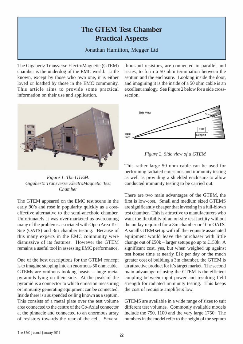
22The EMC Journal January 2011
The Gigahertz Transverse ElectroMagnetic (GTEM)chamber is the underdog of the EMC world. Littleknown, except by those who own one, it is eitherloved or loathed by those in the EMC community.This article aims to provide some practicalinformation on their use and application.
Figure 1. The GTEM.Gigahertz Transverse ElectroMagnetic Test
Chamber
The GTEM appeared on the EMC test scene in theearly 90’s and rose in popularity quickly as a cost-effective alternative to the semi-anechoic chamber.Unfortunately it was over-marketed as overcomingmany of the problems associated with Open Area TestSite (OATS) and 3m chamber testing. Because ofthis many experts in the EMC community weredismissive of its features. However the GTEMremains a useful tool in assessing EMC performance.
One of the best descriptions for the GTEM conceptis to imagine stepping into an enormous 50 ohm cable.GTEMs are ominous looking beasts – huge metalpyramids lying on their side. At the peak of thepyramid is a connector to which emission measuringor immunity generating equipment can be connected.Inside there is a suspended ceiling known as a septum.This consists of a metal plate over the test volumearea connected to the centre of the Co-Axial connectorat the pinnacle and connected to an enormous arrayof resistors towards the rear of the cell. Several
thousand resistors, are connected in parallel andseries, to form a 50 ohm termination between theseptum and the enclosure. Looking inside the door,and imagining it is the inside of a 50 ohm cable is anexcellent analogy. See Figure 2 below for a side cross-section.
Figure 2. Side view of a GTEM
This rather large 50 ohm cable can be used forperforming radiated emissions and immunity testingas well as providing a shielded enclosure to allowconducted immunity testing to be carried out.
There are two main advantages of the GTEM, thefirst is low-cost. Small and medium sized GTEMSare significantly cheaper that investing in a full-blowntest chamber. This is attractive to manufacturers whowant the flexibility of an on-site test facility withoutthe outlay required for a 3m chamber or 10m OATS.A small GTEM setup with all the requisite associatedequipment would leave the purchaser with littlechange out of £50k – larger setups go up to £150k. Asignificant cost, yes, but when weighed up againsttest house time at nearly £1k per day or the muchgreater cost of building a 3m chamber, the GTEM isan attractive product for it’s target market. The secondmain advantage of using the GTEM is the efficientcoupling between input power and resulting fieldstrength for radiated immunity testing. This keepsthe cost of requisite amplifiers low.
GTEMS are available in a wide range of sizes to suitdifferent test volumes. Commonly available modelsinclude the 750, 1100 and the very large 1750. Thenumbers in the model refer to the height of the septum
The GTEM Test ChamberPractical Aspects
Jonathan Hamilton, Megger Ltd

23 The EMC Journal January 2011
and therefore hint at the maximum usable test volume.A GTEM 750 is pictured in Figure 3.
Figure 3. GTEM 750 in use
What are the disadvantages of GTEMs? It dependswho you speak to. Some say that they are acceptablefor full compliance testing of any product within themaximum volume constraints. Others profess thatthe GTEM is not suitable for full compliance testingand are at best useful pre-compliance tools.Resonances due to the internal geometry andequipment cables are the most frequent concerns ofthe EMC fraternity.
How do you use a GTEM? Those who have visitedtest houses will be familiar with radiated emissionsand immunity testing with horizontal and verticalantennae polarisations. The procedure is a littledifferent with the GTEM because its E-field is alwaysvertical. For radiated emissions, the equipment ispositioned in three orthogonal orientations, thereadings are correlated and the resulting graph iseffectively the maximum combination of a traditionalhorizontal and vertical scan on an OATS or traditionalchamber sweep. For immunity, the equipment is alsoilluminated in 3 orientations, although some expertsprofess at least 4 – ideally all 6 faces illuminated bythe RF field. EUT monitoring is the same as in achamber. The benefit of a GTEM being that a windowis present for the observation of the EUT displays, orindicators.
GTEMs are commonly used for radiated emissionstesting to 1GHz and immunity to 2.7GHz – howeverthere is no reason why they cannot be calibrated allthe way to 6GHz to provide full CISPR22 compliancecapability.
The GTEM users group has been around almost aslong as the equipment has existed. It is a friendlygroup, regularly attended by experts who are alwaysready to share experiences. The group has had manyuseful functions – including a strong involvement inthe creation of 61000-4-20 – the GTEM testingstandard which is referenced by some CISPRstandards. The group has a website:www.gtemuser.org.uk and the next meeting is in April2011, see website for the date. Jonathan Hamilton ofMegger Instruments Ltd is the Chairman and can becontacted at: [email protected]
ReferencesFigure 1 courtesy of John Wombwell, EMC Hire Ltd.Figure 2 and Figure 3 courtesy of Howard Chetwin,Measurement Technology Ltd.Thanks to Howard Chetwin of MTL, and RichardMarshall of RML Limited for assistance in producingthis article.
GTEM Members
Jonathan Hamilton (Chairman) Megger LimitedHoward Chetwin (Secretary) Measurement Technology LtdRoger Dixon (Past Chairman) ConsultantApollo Fire DetectorsApplication Solutions Safety & Security Ltd.AR UKAWE AldermastonBaxall SecurityBeka Associates LtdBRE LtdCESGIan Alderman, ConsultantCooper SecurityCST UK LtdData & Information TechnologyDoro UK LtdEC Compliance LtdEchelon Europe LtdElmac ServicesEMC Centre (Paisley) LtdEMC Hire LtdETS-LindgrenExperior Technical Services LtdFCCHMGCCLandis & GyrMariner SystemsNokia UK LtdDivision of Enabling Metrology, NPLNRPBNutwood UK LtdPA ConsultingNigel Carter, ConsultantRichard Marshall LtdSchlumberger ElectricityTeseq LtdTUV Product Service Ltd/BABTUKASUniversity of NottinghamUniversity of York
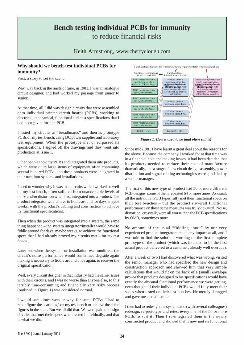
24The EMC Journal January 2011
Why should we bench-test individual PCBs forimmunity?First, a story to set the scene.
Way, way back in the mists of time, in 1981, I was an analoguecircuit designer, and had worked my passage from junior tosenior.
At that time, all I did was design circuits that were assembledonto individual printed circuit boards (PCBs), working toelectrical, mechanical, functional and cost specifications that Ihad been given for that PCB.
I tested my circuits as “breadboards” and then as prototypePCBs on my test bench, using DC power supplies and laboratorytest equipment. When the prototype met or surpassed itsspecifications, I signed off the drawings and they went intoproduction at Issue 1.
Other people took my PCBs and integrated them into products,which were quite large items of equipment often containingseveral hundred PCBs, and these products were integrated intheir turn into systems and installations.
I used to wonder why it was that circuits which worked so wellon my test bench, often suffered from unacceptable levels ofnoise and/or distortion when first integrated into a product. Theproduct integrator would have to fiddle around for days, maybeweeks, with the product’s cabling and construction to achieveits functional specifications.
Then when the product was integrated into a system, the samething happened – the system integrator/installer would have tofiddle around for days, maybe weeks, to achieve the functionalspecs that I had already proved my circuits met – on my testbench.
Later on, when the system or installation was modified, thecircuit’s noise performance would sometimes degrade againmaking it necessary to fiddle around once again, to recover theoriginal specification.
Well, every circuit designer in that industry had the same issueswith their circuits, and I was no worse than anyone else, so thisterribly time-consuming and financially very risky process(outlined in Figure 1) was considered normal.
I would sometimes wonder why, for some PCBs, I had toreconfigure the “earthing” on my test bench to achieve the noisefigures in the spec. But we all did that. We were paid to designcircuits that met their specs when tested individually, and thatis what we did.
Figure 1. How it used to be (and often still is)
Since mid-1981 I have learnt a great deal about the reasons forthe above. Because the company I worked for at that time wasin a financial hole and making losses, it had been decided thatits products needed to reduce their cost of manufacturedramatically, and a range of new circuit design, assembly, powerdistribution and signal cabling technologies were specified bya senior manager.
The first of this new type of product had 50 or more differentPCB designs, some of them repeated 64 or more times. As usual,all the individual PCB types fully met their functional specs ontheir test benches – but the product’s overall functionalperformance on those same measures was truly abysmal. Noise,distortion, crosstalk, were all worse than the PCB specificationsby 60dB, sometimes more.
No amount of the usual “fiddling about” by our veryexperienced product integrators made any impact at all, and Iwas told to find the solution, working on the first completeprototype of the product (which was intended to be the firstactual product delivered to a customer, already well overdue).
After a week or two I had discovered what was wrong, visitedthe senior manager who had specified the new design andconstruction approach and showed him that very simplecalculations that would fit on the back of a (small) envelopeproved that products designed to his specifications would haveexactly the abysmal functional performance we were getting,even though all their individual PCBs would fully meet theirspecs when tested on their test benches. He merely shruggedand gave me a small smile.
I then had to redesign the system, and (with several colleagues)redesign, re-prototype and retest every one of the 50 or morePCBs to suit it. Then I re-integrated them in the newlyconstructed product and showed that it now met its functional
Bench testing individual PCBs for immunity— to reduce financial risks
Keith Armstrong, www.cherryclough.com

25 The EMC Journal January 2011
specifications. This took about 6 months, and the resulting delayin bringing the new product to market harmed the company’sreputation. The company failed a few years later from this andother causes.
End of story.
I have since learned that the reason for all the fiddling about ateach stage of integration was because of a mistakenunderstanding of how currents flowed. Everyone else in thatindustry (and most others) was making the same mistakes atthat time, and many are still.
These mistakes are associated with the idea that alternatingcurrents flow “downhill” until being absorbed by an “earth” or“ground” – that an “earth” or “ground” can be used as somesort of perfect waste disposal system for electrical signals andnoise. It is pure imagination – there is no physical law thateven hints at supporting such a view of current flow.
Many designers of circuits, products, systems and installationsstill make sure they have an “earth” or “ground” on theirelectronic schematics, for reasons of circuit operation and/orEMC rather than safety. Many designers of electronics for carsand airplanes treat their vehicle’s “chassis” as if it was one ofthese impossible current-guzzling “earths” or “grounds”.
Very many magazine articles, and even some conference papersand textbooks, have been written about how best to connectelectronics to “earths” or “grounds”, for functional or EMCreasons. They could all be described as works of fiction,although a better description might be that they are a sharedhallucination – albeit one that has lasted for at least 6 decadesand is still going strong.
In my EMC training courses, articles, papers and books formore than 15 years, I have strongly recommended that the words“earth” or “ground” – and symbols for them – are never usedon electronic schematics, except where they are required forelectrical safety (and then only for that purpose).
For a correct understanding of how currents flow (includingstrays such as CM currents) – and what this means for “earthing”or “grounding” – see [1] or [2] or Chapter 2 of [3], and [4]. Ifyou prefer an academic understanding based solely onMaxwell’s equations, read the first chapters in [5].
My story above is only one of very many examples of hugedelays and huge financial losses caused by thismisunderstanding of how currents really flow. I know of verymany more, and meet them all the time in my work as anindependent EMC consultant.
Conversely, a correct understanding how currents (including“strays”) really flow, and how to design accordingly, makes it(almost) ridiculously easy to deal with most signal integrity(SI), power integrity (PI) and EMC design issues, at PCB,module, product, system and installation levels.
But this is getting away from the purpose of this article, whichis that – when bench-testing a breadboard or prototype circuit– the real electromagnetic environment (usually abbreviated to
EME) of the individual PCB should be applied (or simulatedreasonably well).
In the above story, if we had followed what I propose below,the inadequacy of the product’s overall design would have beenrevealed before any significant project investment. The solutionsI found would have been quickly and easily discovered, andmost likely the new range of products delivered on time andwithout the huge cost over-run and harm to reputation thatactually occurred. It is perhaps too much to believe that thiswould have saved the company, but it would certainly havehelped!
A PCB’s EME includes all the simultaneous electrical “noises”,both radiated and/or conducted, that it will be exposed to by itsintended product(s), system(s), installation(s) and thegeographical location(s) where it will operate; plus all of theelectrical, physical and mechanical issues associated with it,including details of its mounting, enclosure, cabling, and theproximity of other PCBs and objects.
Testing a breadboard or PCB on its own, using standard benchpower supplies and test instruments, cannot tell us anythingabout its likely functional behaviour in real life, when integratedinto a product, system or installation.
When all the PCBs that go into a product meet their functionalspecifications when bench-tested in a way that closely simulatestheir real-life EME, successfully integrating them into the newproduct will only take as long as it takes to assemble the productand perform its verification tests. There will be almost no risksto the project timescales or costs from this late project stage.
Therefore, the answer to the question posed by the title of thissection, is that we should do immunity bench-testing ofindividual PCBs to save time and cost overall, and eliminatealmost all of the financial risks from the product integrationstage.
(There is often an additional benefit, in that PCBs designedand bench-tested like this generally achieve better SI and morerobust software more quickly, helping to reduce time-to-market,improve market reputation, and justify higher selling prices.)
Product functional testing should simulate the EME of thesystems or installations they will be used in. The usual EMCimmunity tests make a stab at this, but for standardisation andrepeatability requirements force a set-up that could be unlikethe product’s real-life EME, and use tests that are unlike itsreal-life EME. That topic is outside the scope of this article,but most of the guides on doing EMC tests in [6] have a chapteron how to modify/extend the usual EMC tests so that they arecloser to “Testing As Real Life” (TARL). Understanding whatthe external EME really is, for a given application, is of coursevital when starting off this process, and [7] provides a usefulguide.
Where errors or malfunctions in electronic circuits or softwarecould possibly increase safety risks, the usual design and testapproaches for compliance with EMC standards, directives orregulations are inadequate and IEC 61508:2010 plus IEC TS61000-1-2 Ed2:2008 should be applied in full. The IET’s guide

26The EMC Journal January 2011
on EMC for Functional Safety [8] provides a great deal ofpractical advice on this, including checklists that can be usedto control and audit the process.
How should we bench-test an individual PCBfor immunity?Figure 2 gives the general idea – the usual testbench instrumentsand AC/DC power supplies are passed through noise couplingcircuits to connect to the PCB, which is assembled in a simulatedproduct enclosure (if the real one isn’t available). Various noisesources also connect to the coupling circuits, to put realisticnoises onto the power, signal, control and data cables.
Figure 2. General overview of bench-testing a PCB for immunity
There are various ways of coupling noise into cables, as shownin Figure 3. We can of course purchase coupling devices, butbetween 150kHz and 1GHz we can make them ourselves quiteeasily, and calibrate them (if we want to) with an RF generatorand spectrum analyser or oscilloscope that that covers thefrequency range we are interested in.
The standard conducted immunity tests, for example IEC/EN61000-4-4, -5, -6, and -16 specify how to design appropriate“coupling-decoupling networks” (CDNs), bulk current injection(BCI) and other coupling devices. These are most suitable whencoupling noise into cables that will be external to the product,so will be tested with such networks in the final productcompliance tests. The ISO 11452 series (automotive EMC),MIL STD 461F and DEF STAN 59-411 (military EMC) includesome additional coupling methods that may be useful or moreappropriate.
The coupling techniques described by standards like these maybe more sophisticated than required when testing a product’sinternal EME. For example, in Figure 2, coupling the noisefrom generators 4a, b, etc. onto internal conductors – sometimesall that is needed to couple a noise generator’s voltage into awire, is a small capacitor.
If a testbench signal generator or analyser has a problem withthe injected noise, we may only need to clip one or two RFsuppression ferrites at its input or output. However, some signalanalysers are very susceptible indeed to RF noise on their inputs,and may need to use a “proper” CDN or other standard-specifiedcoupling device.
Figure 3. Some examples of conducted coupling devices
Figure 2 doesn’t show external or internal radiated fieldgeneration, but there are a number of manufacturers of “desktop” striplines, TEM cell and small “anechoic” test chambers,and if we feel like saving cost we can make our own, see Figure 4.
If our product will have a shielded enclosure, and we areconfident that we’ve got the shielding specifications right, wecould instead test the PCB using only conducted external noiseinjection, and test the shielded enclosure separately withradiated fields to prove its shielding performance againstexternal fields.
A problem with shielded enclosures is that – at their cavityresonance frequencies – internal fields will be magnified, maybe100 or more times (+40dB) than what would occur with anunshielded product enclosure, possibly causing significantcrosstalk that would never appear on a normal bench test. Sowhen the product uses a metal box it can be very important tosimulate realistic internal RF fields. The best simulators arethe PCBs and devices that will generate the fields in real life,but if we don’t yet have them we can use small internal antennasdriven by external RF power amplifiers (the antenna’s coaxbraid always connected to the enclosure wall with a bulkheadcoaxial feedthrough connector).
The radiation efficiency of an antenna is strongly affected bythe RF reflections inside a metal box, making it difficult toensure the correct RF energy is being “launched” inside thebox at all frequencies. However, AET’s spherical dipoles (seeFigure 4) can be used in a “levelling loop” with an RF poweramplifier to generate the specified fields at their location.
Low frequency external and internal fields, say up to 1MHz,can easily be generated by small coils, and checked with othercoils, using the formulae in the guide on IEC 61000-4-8 from[6].

27 The EMC Journal January 2011
Figure 4. Some examples of radiated coupling devices
It’s not as hard as it seems, and there’s a lot to gainRemember the two aspects to realistically simulating a PCBs’EME, mentioned earlier?
a) All the electrical “noises”, both radiated and/orconducted, that the PCB will be exposed to by itsintended product(s), system(s), installation(s) andgeographical location(s) where it could be operated,tested all at the same time.
b) All of the electrical, physical and mechanical issuesassociated with the PCB, including details of itsmounting, enclosure, cabling, and the proximity of otherPCBs and objects.
These issues are discussed in more detail below, and they canseem quite overwhelming at first. However, like everything inelectronic engineering there is a learning curve, and after thefirst such analysis has been done the subsequent ones getprogressively much easier, and for a given range of productsusing a certain set of design technologies a considerable amountof “cut-and-pasting” will become possible. Also, obtaining/making/setting-up the noise generators and coupling deviceswill take some time and cost initially.
After a year or two you will wonder why you ever thought itdifficult, and marvel at how much time and effort this approachwould have saved, if it had been used on earlier projects.
It is important for the analysis of the EME bench-testrequirements for each PCB is done very early in any project,so that the resulting bench-testing specification is an input tothe design process. Then the designer can design accordingly,maybe using low-cost design techniques that are easy to design-in, but would be much more difficult to implement when thedesign had progressed to prototype stage.
At this stage in this sort of discussion, electronic designersusually start to complain about how hard this new approach is,and how much work is involved – as if this was a valid reasonfor ignoring the harsh financial realities of modern productmanufacturing. Electronic engineering is hard to do quicklyand well, and gets harder every year. Get used to it, or find aneasier career (like managing hedge funds).
Usually, designers complain that their managers would neveraccept the extra time/effort/cost – but this only reveals that theyare unable to effectively communicate the real needs of design/development to their managers. This is not the criticism ofdesign engineers that it seems – it is really a criticism of theireducation and training.
In most manufacturing companies the management is entirelyfocussed on financial matters, and very concerned indeed aboutinvestment payback periods and financial risks. Unfortunatelythese are not subjects that design engineers are taught about,so we end up with managers not understanding designengineering and imposing rules on engineers that make no realengineering sense and will actually result in financial harm. (Agood example is the excessive focus on component cost, see[9]).
Design engineers are the only people capable of bridging thiscommunication gap, because understanding how to do cost-effective product design is at least 1,000 times more difficultthan understanding a project’s (really rather simple) financialissues. Plus, the needs of design change with every cycle ofintegrated circuit die-shrinks (i.e. about every two years,according to Moore’s Law).
If, as a design engineer, you don’t want to make the effort tocommunicate what you need to improve your employer’sfinancial success, you just want to keep your head down, dowhat you are told no matter how stupid it is, thinking you canblame the resulting mess on your managers (in fact, they willblame you, even if it was not your fault) – and if you have readthis far – I urge you to change your approach. It is not hard foran electronics design engineer to learn to talk to managers inthe financial terms they understand, and huge corporate andpersonal benefits are there for the taking! A good startingpoint is provided by [9] [10] and [11].
Electrical “noises”Examples of the noises that a PCB is typically exposed to allthe time in normal operation include (but are not limited to):
• Conducted differential-mode (DM) and common-mode(CM) noises on any power, signal, data or control inputor output cable(s) external to the product, which connectdirectly to the PCB, caused by:
o external ambient noises coupling to the externalcable(s)
o the operation of other equipment connected to thecable(s)
• Conducted DM and CM noises on the PCB’s internalAC or DC power supply rail(s), which connect directlyto the PCB, caused by:
o external ambient noises on the product’s AC or DCpower supply cables that have not been completelyattenuated by the product’s power supply filter andconversion circuits

28The EMC Journal January 2011
o the operation of power AC and DC supply convertersand power regulator circuits
o the operation of other loads connected to the samepower supply rail(s)
• Conducted DM and CM noises on any signal, data orcontrol input or output cable(s) internal to the product,which connect directly to the PCB, caused by:
o stray coupling from the magnetic and electric fieldsinside the product
o the operation of other product circuits connected tothe cable(s)
• Stray electric field, magnetic field and electromagneticfield coupling direct to the PCB’s components andtraces, from fields present in the product’s externalambient that are not sufficiently attenuated by theproduct’s shielding.
• Stray magnetic and electric field coupling direct to thePCB’s components and traces from other PCBs, wires,cables, busbars, heatsinks, transformers, etc. inside theproduct.
When we don’t know what internal noises to expect, we canmeasure the noises created by early prototypes of PCBs, or ina similar product that uses similar technologies (maybe even acompetitor’s product, if we intend to use the same ICs, PCBdesign, assembly techniques, etc.). Alternatively, it isincreasingly cost-effective to model them using a computer fieldsolver.
We need to know the noise amplitudes (voltage and/or current),frequency rates and waveshapes, and the tools we use are probes(voltage, current, and close-field types) with oscilloscopes andspectrum analysers. Remember that probe and instrumentbandwidths need to have a bandwidth that is at least 0.35 timesthe reciprocal of the rise/fall time, to measure them at allaccurately (e.g. 1.75 GHz, to measure 0.2ns).
The bench tests should apply the various noises simultaneously,because this is how they occur in real life. Ordinary immunitytesting for complete products applies the various types of testsone at a time, which is not realistic and can lead to problems inthe field. Very little immunity testing has been done onsimultaneous EM disturbances, but [12] shows thatsimultaneous immunity tests easily cause immunity problemseven when a product passes all of the tests if they are done one-at-a-time.
It is easy to see why this can happen, taking the example of adigital processor. Its designers will have striven to keep thesystematic, self-generated noises in its circuitry below its logicthreshold by an amount called the “noise margin”. Externalnoises that disturb the digital signals will “use up” a portion ofthe noise margin, and to avoid over-engineering most designerswould aim to just about pass each type of EMC immunity test,meaning that the additional signal noise from each test used upalmost the full noise margin on its own. Now, when two
disturbances occur together, there is a chance that theircombined noises will exceed the noise margin, causing softwareglitches and other malfunctions.
Unlike most (but not all) external EMEs, all of the various typesof noise in the self-generated EME inside a product are almostalways continually present, so simultaneous internalinterferences are the usual situation.
Electrical, physical and mechanical issuesHere, we are concerned with all the “stray” couplings associatedwith a PCB and its assembled components, and the cables orother conductors that connect to it.
For example, a PCB will have a very different immunity to theelectrical noise it is exposed to, if it is close to a large metalchassis, other metal object, cable, PCB, etc., depending on howit is electrically connected (or not) to that chassis, object, cable,PCB, etc.
Its immunity will also vary depending on exactly how the shieldsof any attached shielded cables are terminated (or not), at oneor both ends, and whether its various connecting wires aretwisted or not.
The outputs of AC and DC power converters should be loadedproperly. If in real life a DC/DC converter will supply 3.3V at10A to a PCB that has 100 off 100nF multilayer ceramicdecoupling capacitors, via 300 mm of twisted-pair wire routedclose to the chassis, then don’t test it with a 3Ω 50W resistorsoldered to its connector pins. Instead, put the resistor and 10µFof multilayer ceramic capacitors on the end of 300mm oftwisted-pair routed close to the chassis like it will be in theproduct. Otherwise the RF stability of the converter, and thecommon-mode RF noise currents it generates, will not be tested.
Driving a CMOS gate input on a different PCB, over a lengthof wire, is not the same as leaving its output connector pinopen-circuit. It requires the same length of the same type ofwire, routed as it will be in real life, connected to a 3 or 4pFcapacitor that is connected to its local 0V reference (usuallyconnected to a different part of the chassis where that PCB willbe mounted) to simulate the CMOS gate’s input capacitance.
3pF has an impedance of 53Ω at 1GHz, lower still at higherfrequencies, hardly something that can be ignored. And thecapacitance of its wire to the chassis or other metalwork willusually be much higher than 3pF.
If the analogue signal or digital data being generated or analysedby the circuits on the tested PCB will in real-life be carried bya 2m-long ribbon cable along with 49 other signals/data, don’tuse just a single short conductor for it. The stray capacitanceand inductance, and the crosstalk in the ribbon cable would notbe present and the measurements would be misleading. Use2m of the correct type of ribbon cable and put in it all the 0Vand power conductors and equivalents to the other signals/dataon the correct conductor numbers (sometimes just one signalor data used 49 times can be used, and often represents a worst-case scenario for crosstalk).
Those readers familiar with computer simulation of the signal

29 The EMC Journal January 2011
integrity or EMC of product assemblies, will know that moreaccurate (i.e. realistic) results are obtained the closer the detailsof the simulated system correspond to real life. It is exactly thesame with this methodology, which could be thought of as“hardware simulation”.
In fact, it is possible to perform computer simulations of circuitsthat are not yet available as prototyped PCBs, to discover whatDM and CM electrical noises they will create, that need to begenerated and coupled – whether radiated and/or conducted –in the bench-test of a prototype PCB assembly as shown inFigure 2.
Saving time during testingSweeping sine-waves over ranges of frequencies is very timeconsuming, and time can be saved by using “time-domain” teststimuli instead. Since the real-life noises in a product’s externaland internal EMEs are complex waveforms anyway, testing withsimilar waveforms is also much more realistic.
For example, switch-mode power converter noise is a series ofpulses with harmonic content up to 1000 times the basic switcherfrequency, so to simulate this – use a conducted noise couplingmethod to inject the output of a digital pulse generator to eachDC power rail, in both CM and DM. Set it to pulse at theswitcher frequency rate with pulse-width and rise/fall timescorresponding to the expected switching waveforms. Suitabledigital pulse generators that will switch in under 10ns can bebought new for under £1,000 (e.g. TG 5011, which will alsoprovide analogue and arbitrary waveforms to over 10MHz).
It would, of course, be much more realistic to power the PCBfrom a prototype of the actual DC power converter it will usein real life – assembled and cabled in the PCB’s chassis as itwill be in the final product. There’s no finer simulation thanthe real thing!
If the DC rail also powers digital circuits on other PCBs,simulate their noise with fast-edged narrow pulses at the clockfrequency(ies). There’s no need to use a digital pulse generatortest instrument, simply make a digital clock generator (or asmany as required) and couple its (their) their clock-bufferedsquare-waves in CM and DM onto the DC rails, using low-value capacitors. Simply vary the value of a capacitor to increasethe voltage noise being injected.
Where a noise has an unknown frequency, or frequency rate –and testing the range of possibilities would take too long –time can be saved by injecting noise only at the PCB’s mostsusceptible frequencies. There are three kinds of susceptiblefrequencies:
1. Due to circuit operation, e.g. the full range of anyanalogue amplifier (test at the frequency at which thesensitivity is the highest); the frequency of any oscillator(analogue or digital) and all of their even and oddnumbered harmonics. Can usually be determined byinspection.
2. Due to the resonances of mechanical, pneumatic,hydraulic, etc. sensors and transducers. Can usually bedetermined by analysis or simple tests.
3. Due to electrical resonances in cables, PCB traces,electrical/electronic components or circuits. Usually bestdetermined by simple voltage or current injection testsover a frequency range, looking for peaks or troughs inthe response of the item being injected into. Injectioncan be direct, taking care not to load the circuit andalter the resonant frequency, or indirect, e.g. by close-field probes.
Beware, RF current clamps often have enoughinductance and stray capacitance to alter a conductor’sresonant frequency. Resonance detection techniquessuch as described in [13] and [14] can be very powerful,for PCB traces, cables or any conductive structures, ofany dimensions and over any frequency range.
ConclusionDesign and bench testing of individual PCBs as outlined above,to meet detailed specifications for their realistic internal andexternal EMEs, is a very powerful way of de-risking theintegration stage of a new product project. Chapter 1.1 of [3]includes some worked examples that make this plain.
Even if the cost and time taken by this technique was the sameas would be required to solve the problems in productintegration that this technique should avoid (they will be less)– the corresponding financial risks to the project would be muchlower.
References[1] The Physical Basis of EMC, Keith Armstrong, The EMC
Journal, Part 1 – Issue 85, November 2009, Part 2 – Issue86, January 2010, Part 3 – Issue 87, March 2010, Part 4 –Issue 88, September 2010
[2] The Physical Basis of EMC, Keith Armstrong, NutwoodUK October 2010, ISBN: 978-0-9555118-3-7, fromwww.emcacademy.org/books.asp
[3] EMC Design Techniques for electronic engineers, KeithArmstrong, Nutwood UK November 2010, ISBN: 978-0-9555118-4-4, from www.emcacademy.org/books.asp
[4] Maxwell’s Equations, Quantum Electrodynamics, and goodinstallation practices for SI, PI and EMC, Keith Armstrong,The EMC Journal, Issue 91, November 2010, pp 32-46,from the archives at www.theemcjournal.com
[5] Grounds for Grounding, Elya B Joffe and Kai-Sang Lock,IEEE Press, John Wiley & Sons, Inc., 2010, ISBN 978-04571-66008-8
[6] Seventeen guides on doing emissions and immunity EMCtesting to IEC and CISPR standards, by Keith Armstrong,free from www.reo.co.uk/knowledgebase
[7] Assessing an Electromagnetic Environment, TechnicalGuidance Note No. 47 (TGN47) from the EMC TestLaboratories Association, free from www.emctla.co.uk/Pages/TechGuideMain.html

30
Free Information from AdvertisersListed below are the Advertisers in the current issueshowing the page number where the company’sadvertisement appears, together with their web addressand email.
11th & 12th October 2011The Racecourse
Newbury
www.emcuk.co.uk
AR Europe OBCwww.ar-europe.ie [email protected]
EMC Hire IBCwww.emchire.co.uk [email protected]
Hursley EMC Services Page 18www.hursley-emc.co.uk [email protected]
Instrument Plastics Page 17www.instrumentplastics.co.uk [email protected]
Kemtron Page 19www.kemtron.co.uk [email protected]
Laplace Instruments Page 3www.laplace.co.uk [email protected]
Rohde & Schwarz UK IFCwww.rohde-schwarz.com [email protected]
Schurter Page 17www.schurter.com [email protected]
Telonic Page 7www.telonic.co.uk [email protected]
Teseq Page 7www.teseq.com [email protected]
TÜV SÜD Product Service Page 4www.tuvps.co.uk [email protected]
The EMC Journal January 2011
[8] EMC and Functional Safety, The IET, 2008, free fromwww.theiet.org/factfiles/emc/emc-factfile.cfm
[9] BOM cost and Profitability, Keith Armstrong, The EMCJournal, Issue 82, May 2009, from the archives atwww.theemcjournal.com
[10]Getting What You Want, Keith Armstrong, The EMCJournal, Issue 77, July 2008, from the archives atwww.theemcjournal.com
[11]Napoleonic Project Management, Keith Armstrong, TheEMC Journal, Issue 80, January 2009, from the archives atwww.theemcjournal.com
[12]Combined Effects of Several, Simultaneous, EMICouplings, Michel Mardiguian, 2000 IEEE Int’l EMCSymp., Washington D.C., Aug 21-25, ISBN 0-7803-5680-2, pp. 181-184.
[13]Measuring Structural Resonances, Doug Smith’s “TechnicalTidbit”, June 2006, http://emcesd.com/tt2006/tt060306.htm
[14]Benchtop EMC Testing Techniques for Medical Equipment– using loop probes to help test devices for electromagneticcompatibility, Scott Roleson, Medical Device & DiagnosticIndustry Magazine, January 1998, www.devicelink.com/mddi/archive/98/01/025.html
Eur Ing Keith Armstrong CEng FIET SMIEEE ACGIphone/fax: +44 (0)1785 660 [email protected]
If you are serious about selling EMC productsor services to Industry...
then you should be a member
The EMCIA was formed on 20th march 2002 for thebenefit of companies involved in Supplying, Designing,
Testing and Manufacturing EMC products.Networking lunches are held 3 times as year.
The current President is Paul Duxbury.
The EMCIA Secretariat is Nutwood UK Ltd., publishersof The EMC Journal, www.theemcjournal.com.
Nutwood UK Ltd., Eddystone Court, De Lank Lane,St Breward, Bodmin, Cornwall, PL30 4NQ
Tel: +44 (0)1208 851530 Fax: +44 (0)1208 851630Email: [email protected] Web: www.emcia.org

31
EMC Hire LimitedIvel Road, Shefford, Bedfordshire SG17 5JU
Tel: 01462 817111 (4 lines) Fax: 01462 819564E-mail: [email protected] Website: www.emchire.co.uk
Full Detailed Cataloguenow available on our website
RF & EMC Test Instrumentationfor Hire plus On-Site Support

32